WO2014010060A1 - 有機エレクトロルミネッセンスデバイス - Google Patents
有機エレクトロルミネッセンスデバイス Download PDFInfo
- Publication number
- WO2014010060A1 WO2014010060A1 PCT/JP2012/067821 JP2012067821W WO2014010060A1 WO 2014010060 A1 WO2014010060 A1 WO 2014010060A1 JP 2012067821 W JP2012067821 W JP 2012067821W WO 2014010060 A1 WO2014010060 A1 WO 2014010060A1
- Authority
- WO
- WIPO (PCT)
- Prior art keywords
- organic
- light
- translucent
- substrate
- bank
- Prior art date
- Legal status (The legal status is an assumption and is not a legal conclusion. Google has not performed a legal analysis and makes no representation as to the accuracy of the status listed.)
- Ceased
Links
Images





Classifications
-
- H—ELECTRICITY
- H10—SEMICONDUCTOR DEVICES; ELECTRIC SOLID-STATE DEVICES NOT OTHERWISE PROVIDED FOR
- H10K—ORGANIC ELECTRIC SOLID-STATE DEVICES
- H10K59/00—Integrated devices, or assemblies of multiple devices, comprising at least one organic light-emitting element covered by group H10K50/00
- H10K59/80—Constructional details
- H10K59/875—Arrangements for extracting light from the devices
- H10K59/878—Arrangements for extracting light from the devices comprising reflective means
-
- H—ELECTRICITY
- H10—SEMICONDUCTOR DEVICES; ELECTRIC SOLID-STATE DEVICES NOT OTHERWISE PROVIDED FOR
- H10K—ORGANIC ELECTRIC SOLID-STATE DEVICES
- H10K2102/00—Constructional details relating to the organic devices covered by this subclass
- H10K2102/301—Details of OLEDs
- H10K2102/302—Details of OLEDs of OLED structures
- H10K2102/3023—Direction of light emission
- H10K2102/3031—Two-side emission, e.g. transparent OLEDs [TOLED]
-
- H—ELECTRICITY
- H10—SEMICONDUCTOR DEVICES; ELECTRIC SOLID-STATE DEVICES NOT OTHERWISE PROVIDED FOR
- H10K—ORGANIC ELECTRIC SOLID-STATE DEVICES
- H10K59/00—Integrated devices, or assemblies of multiple devices, comprising at least one organic light-emitting element covered by group H10K50/00
- H10K59/10—OLED displays
- H10K59/17—Passive-matrix OLED displays
- H10K59/173—Passive-matrix OLED displays comprising banks or shadow masks
Definitions
- the present invention relates to an organic electroluminescence device (hereinafter referred to as an organic EL device) including at least one organic electroluminescence element.
- Organic EL devices are used as surface light sources for lighting equipment as display devices for displaying information such as mobile phones.
- An organic electroluminescent element is configured by, for example, sequentially laminating an anode, an organic layer including a light emitting layer, and a cathode on a transparent glass substrate, and electroluminescence (hereinafter referred to as EL) by current injection from the anode and the cathode to the organic layer.
- EL electroluminescence
- a general organic EL device In a general organic EL device, light emitted from the light emitting layer is taken out through the transparent electrode and the substrate by making the electrode on the substrate side transparent. Most organic EL devices are single-sided flat panels in which light extraction is performed on the front side.
- a double-sided light-emitting organic EL element that directly distributes light from the light-emitting layer to the front side and the back side has also been proposed (see Patent Document 1).
- a technique has also been proposed in which a double-sided light emitting organic EL element is used to provide a reflective material on each of the front and back surfaces thereof to emit light on both sides as a lighting fixture (see Patent Document 2).
- Patent Document 2 has a problem that it is necessary to provide a reflective material on the front side and the back side of the double-sided light emitting organic EL element.
- an example of a problem is to provide an organic EL device capable of maintaining a light intensity toward the front surface and simultaneously emitting faint light to the back surface.
- the organic EL device of the present invention is an organic EL device having at least one organic EL element carried on a translucent substrate that is at least partially translucent, An insulating and translucent non-light emitting portion disposed around the organic EL element on the translucent substrate;
- the organic EL element has an organic layer including a light emitting layer formed between a translucent electrode and a reflective electrode.
- the non-light emitting portion has a light passage portion through which light passes.
- FIG. 1 is a partially cutaway front view of an organic EL device according to an embodiment of the present invention.
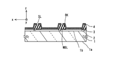
- FIG. 2 is a sectional view taken along the line CC in FIG.
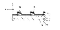
- FIG. 3 is a schematic sectional view of a part of an organic EL device according to another embodiment of the present invention.
- FIG. 4 is a rear view in which the organic EL device of FIG. 1 is partially cut away.
- FIG. 5 is a partially cutaway rear view of an organic EL device according to another embodiment of the present invention.
- FIG. 6 is a partially cutaway rear view of an organic EL device according to still another embodiment of the present invention.
- FIG. 7 is a sectional view taken along the line CC in FIG. FIG.
- FIG. 8 is an enlarged cross-sectional view of a part of the organic EL device of the example.
- FIG. 9 is a schematic sectional view of a part of an organic EL device according to another embodiment of the present invention.
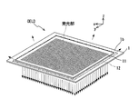
- FIG. 10 is a perspective view of an organic EL device according to another embodiment of the present invention.
- FIG. 11 is a perspective view of a cylindrical table lamp comprising an organic EL device according to another embodiment of the present invention.
- FIG. 12 is a schematic sectional view of a part of an organic EL device according to still another embodiment of the present invention.
- an organic EL device OELD as an embodiment includes a plurality of organic EL elements R, G, and B partitioned by a bank BK that is a non-light-emitting portion on a light-transmitting flat substrate 1 such as glass or resin.
- a bank BK that is a non-light-emitting portion on a light-transmitting flat substrate 1 such as glass or resin.
- Each of the organic EL elements R, G, and B is a strip-shaped light emitting portion that extends in the y direction of the xy main surface of the substrate 1, and emits light from the front surface 1 a of the translucent substrate 1.
- the group of organic EL elements on the back surface of the translucent substrate 1 and the periphery on the bank BK are also non-light emitting portions.
- the bank BK is made of a translucent dielectric material such as optical glass or optical resin.
- the organic EL elements R, G, and B are juxtaposed in parallel, and, for example, emit light of different emission colors of red light emission R, green light emission G, and blue light emission B.
- the organic EL elements of RGB emission colors are arranged as a set in the x direction for each set.
- the organic EL elements R, G, and B that emit red, green, and blue light emission colors are repeatedly arranged in parallel. From the front surface of the substrate 1 that serves as a light extraction surface, red, green, and blue are provided. Are mixed at an arbitrary ratio to emit light that is recognized as a single emission color.
- each of the organic EL elements includes a translucent electrode 2, a metal bus line MBL, an organic layer 3 including a light emitting layer, and a reflective electrode 4 on the back surface 1b of the substrate 1 between the banks BK. It is constructed by stacking.
- This embodiment is a so-called bottom emission type organic EL panel in which light generated in the organic layer 3 is extracted from the front surface of the substrate 1 by applying a voltage between the translucent electrode 2 and the reflective electrode 4. .
- the bank BK is covered with the reflective electrode 4 except for the slot SL.
- the bank BK and the slot SL function as a light passing portion through which light from the substrate 1 and the organic layer 3 passes.
- the strip-shaped translucent electrodes 2 constituting the anode each extend along the y direction on the substrate 1 and are juxtaposed in parallel to the x direction at regular intervals.
- a bus line MBL electrically connected to supply a power supply voltage to the translucent electrode 2 is formed extending along the y direction.
- the metal bus line MBL faces the slot SL. The presence of the metal bus line MBL facing the slot SL makes it possible to adjust the amount of light emitted from the slot SL.
- a bank BK is formed extending along the y direction so as to cover them.
- the metal bus line MBL can be omitted.
- FIG. 4 shows the organic EL device OELD facing from the back surface 1b side of the substrate 1.
- the reflective electrode 4 is formed to extend over the organic EL elements R, G, and B and the bank BK, and a plurality of slots SL are formed along the bank in the reflective electrode 4 on the bank BK as light passing portions. Yes.
- the connection part CON of the reflective electrode 4 is disposed on the top of the bank BK, and the slot SL is formed between the connection parts CON.
- the shape of the slot SL on the bank BK is not limited to an elongated rectangle, and the slot SL may be a short rectangular through-opening as shown in FIG. Furthermore, the through-opening may have a shape such as a circle or an ellipse in addition to the rectangle.
- one slot SL having a narrow gap can be provided for each bank BK. That is, the plurality of independent strip-shaped reflective electrodes 4 extending in the y direction may be formed for each organic EL element.
- the reflective electrode 4 defines at least a part of the bank BK and defines a through-opening that functions as a light passage part.
- the reflective electrode 4 may be formed so as to expose all the banks BK. In these cases, since electric power is supplied from the external wiring (not shown) for each reflective electrode 4, the translucent electrode 2A common to the plurality of organic EL elements is integrated on the substrate 1 as shown in FIG. Can be formed.
- a hole injection layer 3a and a hole transport layer 3b are formed on the transparent electrode 2 between the banks as the organic layer 3.
- the light emitting layer 3c, the electron transport layer 3d, and the electron injection layer 3e are stacked in this order.
- the organic layer 3 sandwiched between the translucent electrode 2 and the reflective electrode 4 is a light emitting laminated body, and is not limited to these laminated structures, for example, hole blocking between the light emitting layer 3c and the electron transporting layer 3d.
- a layered structure including at least a light-emitting layer or a charge transport layer that can also be used, such as adding a layer (not shown), may be used.
- the organic layer 3 may be configured by omitting the hole transport layer 3b, the hole injection layer 3a, or the hole injection layer 3a and the electron transport layer 3d from the stacked structure. May be.
- any known light emitting material such as a fluorescent material or a phosphorescent material can be applied.
- Examples of fluorescent materials that emit blue light include naphthalene, perylene, and pyrene.
- fluorescent materials that give green light emission include quinacridone derivatives, coumarin derivatives, and aluminum complexes such as Alq3 (tris (8-hydroxy-quinoline) aluminum).
- Examples of fluorescent materials that give yellow light include rubrene derivatives.
- Examples of fluorescent materials that give red light emission include DCM (4- (dicyanomethylene) -2-methyl-6- (p-dimethylaminostyryl) -4H-pyran) compounds, benzopyran derivatives, rhodamine derivatives, and the like.
- Examples of the phosphorescent material include iridium, platinum, ruthenium, rhodium, and palladium complex compounds. Specific examples of the phosphorescent material include tris (2-phenylpyridine) iridium (so-called Ir (ppy) 3), tris (2-phenylpyridine) ruthenium, and the like.
- Known methods for forming the organic layer 3 include dry coating methods such as sputtering and vacuum deposition, and wet coating methods such as screen printing, spraying, ink jetting, spin coating, gravure printing, and roll coater. ing.
- dry coating methods such as sputtering and vacuum deposition
- wet coating methods such as screen printing, spraying, ink jetting, spin coating, gravure printing, and roll coater.
- the hole injection layer, the hole transport layer, and the light emitting layer are uniformly formed by a wet coating method
- the electron transport layer and the electron injection layer are sequentially formed uniformly by a dry coating method.
- a film may be formed.
- all the functional layers may be sequentially formed in a uniform film thickness by a wet coating method.
- the anode translucent electrode 2 for supplying holes to the functional layers up to the light emitting layer 3c includes ITO (Indium-tin-oxide), ZnO, ZnO—Al 2 O 3 (so-called AZO), In 2 O 3 ⁇ . It may be composed of ZnO (so-called IZO), SnO 2 —Sb 2 O 3 (so-called ATO), RuO 2 or the like. Furthermore, for the translucent electrode 2, it is preferable to select a material having a transmittance of at least 10% at the emission wavelength obtained from the light emitting layer.
- the translucent electrode 2 usually has a single-layer structure, but it can also have a laminated structure made of a plurality of materials if desired.
- the cathode reflective electrode 4 that supplies electrons to the functional layers up to the light emitting layer 3c is not limited, and for example, metals such as aluminum, silver, copper, nickel, chromium, gold, and platinum are used. In addition, these materials may be used only by 1 type and may use 2 or more types together by arbitrary combinations and a ratio.
- the material of the reflective electrode 4 preferably includes a metal having a low work function in order to efficiently inject electrons.
- a suitable metal such as tin, magnesium, indium, calcium, aluminum, silver, or an alloy thereof. Is used. Specific examples include low work function alloy electrodes such as magnesium-silver alloy, magnesium-indium alloy, and aluminum-lithium alloy.
- the reflective electrode 4 can be formed as a single layer film or a multilayer film on the organic layer 3 by sputtering or vacuum deposition.
- the organic layer 3 is sandwiched between the translucent electrode 2 and the reflective electrode 4, a driving voltage is applied to the organic layer 3 via the translucent electrode 2 and the reflective electrode 4.
- a driving voltage is applied to the organic layer 3 via the translucent electrode 2 and the reflective electrode 4.
- the light generated in the light-emitting layer 3c in the organic layer 3 passes through the translucent electrode 2, and after being reflected by the reflective electrode 4, passes through the translucent electrode 2 and passes through the film. If processing such as sticking is not performed, about 20% is taken out from the front surface of the translucent substrate 1.
- light L1 less than the critical angle of each interface of the light passes through the translucent electrode 2 and travels to the glass substrate 1, and the light L2 directed to the other reflective electrode 4 is reflected there and is emitted.
- the light passes through the translucent electrode 2 to the glass substrate 1, and the light is emitted to the front space of the substrate 1.
- the light L3 exceeding the remaining critical angle is totally reflected and travels toward the bank BK.
- a part of the light emitted from the end face of the light emitting layer 3c or the light L4 directed in the lateral direction enters the bank BK, and the rest is totally reflected in each layer.
- the light entering the bank BK is radiated from the bank BK to the space on the back side of the substrate 1 through the slot SL after direct or several reflections. If the intervals between the banks are formed at a constant period, the plurality of slots opened on the back side are evenly distributed, so that unevenness of the back side emitted light does not occur. Therefore, according to the present embodiment, it is possible to extract a part of the light absorbed by the bank portion that has been conventionally opaque and the light toward the front surface of the substrate as light light on the back surface side of the substrate.
- This embodiment conventionally uses light absorbed by the substrate or bank to maintain the intensity of the radiated light toward the front surface of the substrate, and emits faint light on the back side of the substrate without providing a reflector on the front surface side. Can be taken out from.
- a light-transmitting material that covers and seals the light-emitting portions of the plurality of organic EL elements formed on the back surface 1b of the substrate 1 is used.
- a sealing member 11 is provided.
- a glass dish-shaped transparent sealing cap may be used for the translucent sealing member 11.
- the transparent sealing cap is fixed to the periphery of the light-emitting part with an adhesive so as to cover the light-emitting part, and hermetically protects the light-emitting part.
- the inside of the transparent sealing cap may be sealed by filling with an inert gas or an inert liquid.
- the translucent sealing member 11 a transparent resin such as polyparaxylylene, or a gas barrier sealing film composed of a multilayer of an inorganic film such as a silicon oxide film and an organic film can be used.
- the light emitting part of the organic EL element is configured not to contact moisture and oxygen in the atmosphere by the sealing member 11.
- the organic EL device OELD includes a transmission diffusion portion 12 that is a light passage portion extending on the back surface 1 b of the translucent substrate 1 disposed around the sealing member 11.
- the permeation diffusion portion 12 can be formed as a rough surface composed of a plurality of minute irregularities by a processing method such as etching or sandblasting performed on a predetermined portion of the back surface of the substrate 1. A part of the light traveling toward the end surface while propagating through the translucent substrate 1 by total reflection can be taken out from the back surface 1b of the substrate by the transmission diffusion portion 12.
- FIG. 11 shows an example of a tubular table lamp in the form of a row lamp composed of the organic EL device OELD.
- the cylindrical desk lamp includes a rectangular tubular body 20 that is a light emitter, leg portions 21 that extend from the four corners of the rectangular tubular body, and a base 22 that fixes the leg portions.
- the rectangular cylinder 20 is constructed by assembling four panels of the same rectangular organic EL device OELD with the front surface facing outward and the back surface facing inward.
- the cylindrical desk lamp is lit indoors, when the room is bright, the light from the back of the organic EL device OELD (that is, the light inside the rectangular cylinder 20) is not noticed by the user, and the room When it is dark, the user can recognize it as a faint light inside the rectangular tube 20.
- a quartz or glass plate, a metal plate or metal foil, a bent resin substrate, a plastic film, a sheet, or the like is used as the translucent substrate 1.
- a glass plate or a transparent plate made of a synthetic resin such as polyester, polymethacrylate, polycarbonate, or polysulfone is preferable.
- a synthetic resin substrate it is necessary to pay attention to gas barrier properties. If the gas barrier property of the substrate is too small, the organic EL device may be deteriorated by outside air that has passed through the substrate, which is not preferable. Therefore, a method of securing a gas barrier property by providing a dense silicon oxide film or the like on at least one surface of the synthetic resin substrate is also a preferable method.
- a light extraction film (not shown) may be attached to the front surface of the substrate 1 so as to cover the light emitting portion.
- a so-called bottom emission type organic EL panel in which the translucent electrode 2 is formed on the back surface of the translucent substrate 1 and the light generated in the organic layer 3 is extracted from the front surface of the substrate 1 is described.
- an organic EL device that is a so-called top emission type organic EL panel can be configured.
- the reflective electrode 4 is formed on the substrate 1 between the banks BK, and the organic layer 3 including the light emitting layer and the light transmitting layer are formed thereon.
- the conductive electrode 2 is laminated.
- the reflective electrode 4 defines a slot SL as a through opening that contacts the bank BK and the substrate 1.
- the bank BK and the slot SL function as a light passage portion through which light from the organic layer 3 passes. In this example as well, a part of the light absorbed in the bank part and the light on the front face of the bank can be extracted as light light to the substrate.
- all of the substrate 1 is a translucent example, but the substrate 1 only needs to be translucent at least in the slot portion.
- the organic layer is a light-emitting laminate, but the light-emitting laminate can also be formed by laminating inorganic material films.
- the present invention is not limited to this, and a laminated structure or a mixture of light emitting layers such as a tandem structure each composed of a plurality of light emitting layers. The same effect can be obtained even when a plurality of white light emitting organic EL elements using the light emitting layer are juxtaposed.
Landscapes
- Electroluminescent Light Sources (AREA)
Description
本発明は、少なくとも1つの有機エレクトロルミネッセンス素子を含む有機エレクトロルミネッセンスデバイス(以下、有機ELデバイスと称する)に関する。
有機ELデバイスは、携帯電話機などの情報を表示する表示装置として、照明器具の面光源として、利用されている。有機エレクトロルミネッセンス素子は、例えば、透明ガラス基板上に陽極、発光層を含む有機層及び陰極を順次積層して構成され、陽極及び陰極から有機層への電流注入により、エレクトロルミネッセンス(以下、ELと称する)を発現する発光素子である。
一般的な有機ELデバイスは、発光層からの発光光が、基板側の電極を透明とすることにより、この透明電極と基板を介して取り出される。ほとんどの有機ELデバイスは光取り出しが前面側へ行われる片面発光の平面パネルである。また、発光層からの光を前面側と背面側にそのまま振り分ける両面発光有機EL素子も提案されている(特許文献1参照)。さらに、両面発光有機EL素子を利用して、その前面と背面とにそれぞれ反射材を設け、照明器具として両面発光させる技術も提案されている(特許文献2参照)。
ところが、有機ELデバイスでは、発光層からの発光光の一部が透明電極-ガラス界面間及びガラス-空気界面間での全反射により閉じ込められて消衰する故に、発光層からの発光光のうち数十%程度の光しか外部に取り出すことができないと言われている。
特許文献1の技術においては、透明基板内を伝搬する光がその基板内で減衰してしまうとともに基板端面まで伝搬する光がそこで端面から漏れ出すという問題があった。
また、特許文献2に開示された技術では、さらに、両面発光有機EL素子の前面と背面側にそれぞれ反射材を設ける必要が生じるという問題があった。
そこで、本発明では、前面への光強度を維持すると同時に背面に仄かな光を放射できる有機ELデバイスを提供することが課題の一例として挙げられる。
本発明の有機ELデバイスは、少なくとも一部が透光性である透光性基板上に担持された少なくとも1つの有機EL素子を有する有機ELデバイスであって、
前記透光性基板上の前記有機EL素子の周辺に配置された絶縁性且つ透光性の非発光部を有し、
前記有機EL素子は透光性電極及び反射電極の間に形成されて発光層を含む有機層を有し、
前記非発光部は光が通過する光通過部を有することを特徴とする。
前記透光性基板上の前記有機EL素子の周辺に配置された絶縁性且つ透光性の非発光部を有し、
前記有機EL素子は透光性電極及び反射電極の間に形成されて発光層を含む有機層を有し、
前記非発光部は光が通過する光通過部を有することを特徴とする。
以下に本発明の実施例を図面を参照しつつ説明する。
図1において、実施例である有機ELデバイスOELDは、ガラスや樹脂などの光透過性平板の基板1上に非発光部であるバンクBKによって区画された複数の有機EL素子R、G及びBを含んでいる。有機EL素子R、G及びBは、それぞれが基板1のxy主面のy方向に伸長するストリップ形状の発光部であり、透光性基板1の前面1aから光を放射する。なお、透光性基板1の背面の有機EL素子の群とバンクBK上の周辺も非発光部である。バンクBKは例えば光学ガラスや光学樹脂などの透光性誘電体材料から形成される。有機EL素子R、G及びBは平行に並置され、例えば、赤色発光R、緑色発光G及び青色発光Bの互いに異なる発光色の光を放射する。RGB発光色の有機EL素子を一組としてx方向に組毎に並べられている。
このように、赤、緑、青の発光色をそれぞれ発する有機EL素子R、G及びBは、平行に繰り返し配置されており、光取り出し面となる基板1の前面からは、赤、緑、青の光が任意の割合で混色されて単一の発光色として認識される光が放出される。
図2に示すように、有機EL素子の各々は、バンクBK間の基板1の背面1b上に、透光性電極2、金属のバスラインMBL、発光層を含む有機層3、反射電極4が積層されて構成される。本実施例は、透光性電極2と反射電極4との間に電圧を印加することにより、有機層3において生成される光を基板1の前面から取り出す所謂ボトムエミッション型の有機ELパネルである。バンクBKはスロットSLを除き反射電極4により覆われている。バンクBKとスロットSLは基板1と有機層3からの光が通過する光通過部として機能する。
陽極を構成するストリップ形状の透光性電極2は、それぞれ基板1上においてy方向に沿って伸長し、互いに一定間隔おいてx方向に平行に並置されている。
透光性電極2の各々の端側上には、透光性電極2に電源電圧を供給する為に電気的に接続されたバスラインMBLがy方向に沿って伸長して形成されている。金属バスラインMBLはスロットSLに対向している。スロットSLに対向している金属バスラインMBLが存在することにより、スロットSLから放射される光の量を調節することができる。
基板1及び透光性電極2のバスラインMBL上にはこれらを覆うようにバンクBKがy方向に沿って伸長して形成されている。
なお、図2に示す有機ELデバイスでは、金属バスラインMBLを介して透光性電極2に電源電圧を供給する構成を示しているが、他の実施例においては、図3に示すように、金属バスラインMBLを省略することもできる。
図4は基板1の背面1b側から臨む有機ELデバイスOELDを示す。反射電極4は有機EL素子R、G及びBとバンクBK上へ掛け渡されて形成され、さらに、光通過部として複数のスロットSLがバンクBK上の反射電極4にバンクに沿って形成されている。この場合、バンクBK上の頂部に反射電極4の接続部CONが配置され、接続部CON間にスロットSLが形成されている。
バンクBK上のスロットSLの形状は細長い矩形に限定されず、図5に示すように、スロットSLは短い矩形の貫通開口としてもよい。さらに、貫通開口は矩形以外に円形、楕円形などの形状としても良い。
また、図6に示すように、バンクBK毎に一本の細長い隙間のスロットSLを設けることができる。すなわち、y方向に伸長する複数の独立したストリップ形状の反射電極4は、有機EL素子毎に形成されてもよい。このように、反射電極4は、バンクBKの少なくとも一部を露出させ光通過部として機能する貫通開口を画定する。反射電極4は、バンクBKをすべて露出させるように形成されてもよい。これらの場合、反射電極4ごとに外部配線(図示せず)から電力を供給される故に、図7に示すように、複数の有機EL素子に共通する透光性電極2Aが基板1上に一体的に形成され得る。
図8に示すように、上記の何れの形態の有機ELデバイスにおいても、バンクの間の透光性電極2の上には、有機層3として、例えば正孔注入層3a、正孔輸送層3b、発光層3c、電子輸送層3d及び電子注入層3eが順に積層されている。透光性電極2と反射電極4の間に挟持された有機層3は発光積層体であり、これら積層構成に限定されることなく、例えば発光層3cと電子輸送層3dの間に正孔阻止層(図示せず)を追加するなど、少なくとも発光層を含み、或いは兼用できる電荷輸送層を含む積層構成であってもよい。有機層3は、上記積層構造から正孔輸送層3bを省いて構成しても、正孔注入層3aを省いて構成しても、正孔注入層3aと電子輸送層3dを省いて構成してもよい。
発光層3cの発光材料としては、例えば、蛍光材料や燐光材料など、任意の公知の発光材料が適用可能である。
青色発光を与える蛍光材料としては、例えば、ナフタレン、ペリレン、ピレンなどが挙げられる。緑色発光を与える蛍光材料としては、例えば、キナクリドン誘導体、クマリン誘導体、Alq3(tris (8-hydroxy-quinoline) aluminum) などのアルミニウム錯体などが挙げられる。黄色発光を与える蛍光材料としては、例えば、ルブレン誘導体などが挙げられる。赤色発光を与える蛍光材料としては、例えば、DCM(4-(dicyanomethylene)-2-methyl-6-(p-dimethylaminostyryl)-4H-pyran)系化合物、ベンゾピラン誘導体、ローダミン誘導体などが挙げられる。燐光材料としては、例えば、イリジウム、白金、ルテニウム、ロジウム、パラジウムの錯体化合物などが挙げられる。燐光材料として、具体的には、トリス(2-フェニルピリジン)イリジウム(所謂、Ir(ppy)3)、トリス(2-フェニルピリジン)ルテニウムなどが挙げられる。
有機層3を成膜する手法として、スパッタリング法や真空蒸着法などの乾式塗布法や、スクリーン印刷、スプレー法、インクジェット法、スピンコート法、グラビア印刷、ロールコータ法などの湿式塗布法が知られている。例えば、正孔注入層、正孔輸送層、発光層を湿式塗布法で膜厚を均一に成膜して、電子輸送層及び電子注入層を、それぞれ乾式塗布法で膜厚を均一に順次成膜してもよい。また、すべての機能層を湿式塗布法で膜厚を均一に順次成膜してもよい。
発光層3cまでの機能層に正孔を供給する陽極の透光性電極2は、ITO(Indium-tin-oxide)やZnO、ZnO-Al2O3(所謂、AZO)、In2O3-ZnO(所謂、IZO)、SnO2-Sb2O3(所謂、ATO)、RuO2などにより構成され得る。さらに、透光性電極2は、発光層から得られる発光波長において少なくとも10%以上の透過率を持つ材料を選択することが好ましい。
透光性電極2は通常は単層構造であるが、所望により複数の材料からなる積層構造とすることも可能である。
発光層3cまでの機能層に電子を供給する陰極の反射電極4には、限定されないが、例えば、アルミニウム、銀、銅、ニッケル、クロム、金、白金などの金属が使われる。なお、これらの材料は、1種のみで用いてもよく、2種以上を任意の組み合わせ及び比率で併用してもよい。
反射電極4の材料としては、効率良く電子注入を行う為に仕事関数の低い金属が含まれることが好ましく、例えば、スズ、マグネシウム、インジウム、カルシウム、アルミニウム、銀などの適当な金属又はそれらの合金が用いられる。具体例としては、マグネシウム-銀合金、マグネシウム-インジウム合金、アルミニウム-リチウム合金などの低仕事関数合金電極が挙げられる。
反射電極4はスパッタ法や真空蒸着法などにより有機層3上に、単層膜、又は多層膜として形成され得る。
次に、図9を用いて、上記の有機ELデバイスの動作を説明する。なお、上記実施例と同一符号で示した構成部分は、上記実施例の有機ELデバイスと同様であるので、それらの詳しい説明は省略する。
有機ELデバイスにおいては、有機層3は透光性電極2及び反射電極4の間に接して挟持されている故に、透光性電極2と反射電極4とを介して有機層3に駆動電圧が印加されることにより、有機層3内の発光層3cにおいて生成された光は透光性電極2を通過して、さらに反射電極4で反射した後に透光性電極2を通過して、フィルムを貼るなどの処理を行わないと20%程度が透光性基板1の前面から取り出される。
発光層3cから発光した光は、そのうちの各界面の臨界角未満の光L1が透光性電極2を通りガラス基板1へ進み、他の反射電極4へ向かう光L2はそこで反射され発光層3cと透光性電極2を通りガラス基板1へ進み、それらの光は基板1の前面空間へ放射される。残りの臨界角を超える光L3は全反射し、バンクBKへ向かう。一方、発光層3cの端面から発光した光や横方向へ向かう光L4は一部がバンクBK内に入り、残りは各層内で全反射する。これらバンクBKに入った光は直接または数回の反射の後、バンクBKから、スロットSLを経て、基板1の背面側空間へ放射される。なお、バンクとバンクの間隔を一定周期で形成すれば、背面側に開口された複数のスロットが均一に分布するので、背面側放射光のむらは生じない。よって、本実施例によれば従来不透明であるバンク部分で吸収される光や基板前面への光の一部を基板背面側にも淡い光として取り出すことができる。
本実施例は、従来、基板やバンクに吸収される光を利用することで、基板前面への放射光の強度を維持し、前面側に反射材を設けることなく仄かな光を基板の背面側から取り出すことができる。
次に、図10に示すように、上記の何れの形態の有機ELデバイスにおいて、基板1の背面1bに形成された複数の有機EL素子の発光部を覆い且つこれらを封止する透光性の封止部材11が設けられている。透光性の封止部材11には、ガラス製の皿状の透明封止キャップが用いられ得る。透明封止キャップは発光部を覆うようにその周囲に接着剤を介して固定され発光部を密閉保護する。透明封止キャップの内部は不活性気体又は不活性液体を充填することにより封止されてもよい。また、透光性の封止部材11として、ポリパラキシリレンなどの透明樹脂や、シリコン酸化膜などの無機膜と有機膜の多層からなるガスバリア性封止膜が用いられ得る。このように、封止部材11により有機EL素子の発光部は大気中の水分及び酸素と接しないように構成されている。
また、図10に示すように、有機ELデバイスOELDは、封止部材11の周辺に配置された透光性基板1の背面1b上に延在する光通過部である透過拡散部12を含む。透過拡散部12は、基板1の背面の所定部位上に施すエッチングやサンドブラストなどの加工法により、複数の微小凹凸からなる粗面として形成され得る。透過拡散部12により、透光性基板1内を全反射で伝搬しつつ端面へ向かう光の一部を、拡散させつつ基板の背面1bから取り出すことができる。
さらに、図11は上記の有機ELデバイスOELDからなる行灯形態の筒状電気スタンドの一例を示す。筒状電気スタンドは、発光体である四角筒体20と、四角筒体の四隅から延びる脚部21と、脚部を固定する台座22とを含む。四角筒体20は、4枚の同一矩形形状の有機ELデバイスOELDのパネルを、それぞれの前面を外部に向け背面を内部に向けて組み立てられて構成されている。筒状電気スタンドを屋内で点灯使用すれば、部屋が明るい時は有機ELデバイスOELDの背面からの光(すなわち四角筒体20の内側の光)は使用者には気にはならず、部屋が暗い時は四角筒体20の内側の仄かな光として使用者が認識できるようになる。
なお、上記の何れの実施例では、透光性基板1として、石英やガラスの板、金属板や金属箔、曲げられる樹脂基板、プラスチックフィルムやシートなどが用いられる。特にガラス板や、ポリエステル、ポリメタクリレート、ポリカーボネート、ポリスルホンなどの合成樹脂の透明板が好ましい。合成樹脂基板を使用する場合にはガスバリア性に留意する必要がある。基板のガスバリア性が小さすぎると、基板を通過した外気により有機ELデバイスが劣化することがあるので好ましくない。よって、合成樹脂基板の少なくとも片面に緻密なシリコン酸化膜などを設けてガスバリア性を確保する方法も好ましい方法の一つである。
なお、出力光の取り出し効率を上げるために、基板1の前面に、発光部を覆うように、これを超える面積で光取り出しフィルム(図示せず)を取り付けてもよい。
さらに、上記実施例では、透光性電極2が透光性基板1の背面上に形成されて有機層3において生成される光を基板1の前面から取り出す所謂ボトムエミッション型の有機ELパネルを説明したが、更なる実施例においては、所謂トップエミッション型の有機ELパネルとした有機ELデバイスも構成できる。
例えば、図12に示すように、トップエミッション有機ELデバイスの有機EL素子の各々は、バンクBK間の基板1上に反射電極4が形成され、その上に発光層を含む有機層3及び透光性電極2が積層されて構成される。この例では、透光性電極2と反射電極4の間に電圧を印加することにより、有機層3において生成される光がほとんど透光性電極2側から取り出される。反射電極4は、バンクBKと基板1を接触させる貫通開口としてスロットSLを画定している。バンクBKとスロットSLは有機層3からの光が通過する光通過部として機能する。この例でも、バンク部分で吸収される光やバンク前面への光の一部を基板へ淡い光として取り出すことができる。
図12の実施例では基板1のすべてを透光性の例としたが、基板1は少なくともスロット部分のみ透光性であればよい。
また、上記の実施例では有機層を発光積層体としているが、無機材料膜の積層によっても発光積層体を構成できる。
また、上記実施例では複数の有機EL素子R、G及びBを並置した例で示したが、これには限定されず、各々が複数の発光層からなるタンデム構造など発光層の積層構造や混合発光層を利用した複数の白色発光有機EL素子を並置した場合でも同様の効果が得られる。
1 基板
2 透光性電極
3 有機層
3a 正孔注入層
3b 正孔輸送層
3c 発光層
3d 電子輸送層
3e 電子注入層
4 反射電極
11 封止部材
12 透過拡散部
BK バンク
MBL バスライン
2 透光性電極
3 有機層
3a 正孔注入層
3b 正孔輸送層
3c 発光層
3d 電子輸送層
3e 電子注入層
4 反射電極
11 封止部材
12 透過拡散部
BK バンク
MBL バスライン
Claims (6)
- 少なくとも一部が透光性である透光性基板上に担持された少なくとも1つの有機EL素子を有する有機ELデバイスであって、
前記透光性基板上の前記有機EL素子の周辺に配置された絶縁性且つ透光性の非発光部を有し、
前記有機EL素子は透光性電極及び反射電極の間に形成されて発光層を含む有機層を有し、
前記非発光部は光が通過する光通過部を有することを特徴とする有機ELデバイス。 - 前記透光性電極が前記透光性基板上に形成され、
前記非発光部は前記有機EL素子を区画する透光性誘電体材料のバンクを含み、
前記反射電極が前記バンクの少なくとも一部を露出させる貫通開口を前記光通過部として画定することを特徴とする請求項1に記載の有機ELデバイス。 - 前記反射電極が前記有機層から前記バンク上へ掛け渡されて形成され、前記貫通開口は前記バンク上の前記反射電極に形成されたスロットであることを特徴とする請求項2に記載の有機ELデバイス。
- 前記バンクと前記有機EL素子を覆い且つこれらを封止する透光性の封止部材を有することを特徴とする請求項2に記載の有機ELデバイス。
- 前記光通過部は前記封止部材の周辺の前記透光性基板上に延在することを特徴とする請求項4に記載の有機ELデバイス。
- 前記反射電極が前記透光性基板上に形成され、
前記非発光部は前記有機EL素子を区画する透光性誘電体材料のバンクを含み、
前記反射電極が前記バンクと前記透光性基板とを接触させる貫通開口を前記光通過部として画定することを特徴とする請求項1に記載の有機ELデバイス。
Priority Applications (1)
| Application Number | Priority Date | Filing Date | Title |
|---|---|---|---|
| PCT/JP2012/067821 WO2014010060A1 (ja) | 2012-07-12 | 2012-07-12 | 有機エレクトロルミネッセンスデバイス |
Applications Claiming Priority (1)
| Application Number | Priority Date | Filing Date | Title |
|---|---|---|---|
| PCT/JP2012/067821 WO2014010060A1 (ja) | 2012-07-12 | 2012-07-12 | 有機エレクトロルミネッセンスデバイス |
Publications (1)
| Publication Number | Publication Date |
|---|---|
| WO2014010060A1 true WO2014010060A1 (ja) | 2014-01-16 |
Family
ID=49915562
Family Applications (1)
| Application Number | Title | Priority Date | Filing Date |
|---|---|---|---|
| PCT/JP2012/067821 Ceased WO2014010060A1 (ja) | 2012-07-12 | 2012-07-12 | 有機エレクトロルミネッセンスデバイス |
Country Status (1)
| Country | Link |
|---|---|
| WO (1) | WO2014010060A1 (ja) |
Citations (3)
| Publication number | Priority date | Publication date | Assignee | Title |
|---|---|---|---|---|
| JP2002202737A (ja) * | 2000-12-28 | 2002-07-19 | Nec Corp | 発光素子の製造方法、発光素子 |
| JP2009238833A (ja) * | 2008-03-26 | 2009-10-15 | Sony Corp | 画像表示装置 |
| JP2010009793A (ja) * | 2008-06-24 | 2010-01-14 | Canon Inc | 発光素子、発光素子を用いた表示装置及び発光素子の製造方法 |
-
2012
- 2012-07-12 WO PCT/JP2012/067821 patent/WO2014010060A1/ja not_active Ceased
Patent Citations (3)
| Publication number | Priority date | Publication date | Assignee | Title |
|---|---|---|---|---|
| JP2002202737A (ja) * | 2000-12-28 | 2002-07-19 | Nec Corp | 発光素子の製造方法、発光素子 |
| JP2009238833A (ja) * | 2008-03-26 | 2009-10-15 | Sony Corp | 画像表示装置 |
| JP2010009793A (ja) * | 2008-06-24 | 2010-01-14 | Canon Inc | 発光素子、発光素子を用いた表示装置及び発光素子の製造方法 |
Similar Documents
| Publication | Publication Date | Title |
|---|---|---|
| JP6074423B2 (ja) | 有機エレクトロルミネッセンスデバイス | |
| JP6751459B2 (ja) | 有機エレクトロルミネッセンス照明パネル、その製造方法及び有機エレクトロルミネッセンス照明装置 | |
| JP5477963B2 (ja) | 透過型カラー有機el表示装置 | |
| KR102421582B1 (ko) | 유기 발광 표시 장치 및 그 제조 방법 | |
| US20120268001A1 (en) | Organic light-emitting display device and method of manufacturing the same | |
| US9960382B2 (en) | Organic electroluminescence element, display panel, and method for manufacturing organic electroluminescence element | |
| JP2005158371A (ja) | 有機エレクトロルミネセンス素子とその製造方法、および照明装置 | |
| JP2009252458A (ja) | 有機エレクトロルミネセンス素子 | |
| CN110391280A (zh) | 一种电致发光的显示和照明装置及其制备方法 | |
| JP2005158372A (ja) | エレクトロルミネセンス素子及び照明装置 | |
| CN115377323A (zh) | 一种显示面板及显示装置 | |
| TW201740553A (zh) | 有機電致發光顯示裝置 | |
| WO2014010060A1 (ja) | 有機エレクトロルミネッセンスデバイス | |
| JP5330655B2 (ja) | 有機el表示装置 | |
| KR20120035027A (ko) | 유기 발광 장치 및 이를 이용한 조명 장치 | |
| JP6238126B2 (ja) | 発光素子及びそれを用いた照明装置 | |
| WO2013186919A1 (ja) | 有機エレクトロルミネッセンスデバイス | |
| US9373810B2 (en) | Organic EL element and light-emitting apparatus including the same | |
| JP5943405B2 (ja) | 有機el照明装置及びその製造方法 | |
| WO2013186916A1 (ja) | 有機エレクトロルミネッセンスデバイス | |
| JPWO2016042921A1 (ja) | 発光装置 | |
| WO2013168228A1 (ja) | 有機エレクトロルミネッセンスデバイス | |
| WO2017029889A1 (ja) | 有機elパネル、照明装置、並びに、有機elパネルの製造方法 | |
| JP2016181360A (ja) | 有機エレクトロルミネッセンスパネル及び照明装置 | |
| WO2013186918A1 (ja) | 有機エレクトロルミネッセンスデバイス |
Legal Events
| Date | Code | Title | Description |
|---|---|---|---|
| 121 | Ep: the epo has been informed by wipo that ep was designated in this application |
Ref document number: 12881066 Country of ref document: EP Kind code of ref document: A1 |
|
| NENP | Non-entry into the national phase |
Ref country code: DE |
|
| 122 | Ep: pct application non-entry in european phase |
Ref document number: 12881066 Country of ref document: EP Kind code of ref document: A1 |