WO2014009991A1 - 3次元構造のmosfet及びその製造方法 - Google Patents
3次元構造のmosfet及びその製造方法 Download PDFInfo
- Publication number
- WO2014009991A1 WO2014009991A1 PCT/JP2012/004428 JP2012004428W WO2014009991A1 WO 2014009991 A1 WO2014009991 A1 WO 2014009991A1 JP 2012004428 W JP2012004428 W JP 2012004428W WO 2014009991 A1 WO2014009991 A1 WO 2014009991A1
- Authority
- WO
- WIPO (PCT)
- Prior art keywords
- region
- silicide
- layer
- basic electronic
- channel region
- Prior art date
- Legal status (The legal status is an assumption and is not a legal conclusion. Google has not performed a legal analysis and makes no representation as to the accuracy of the status listed.)
- Ceased
Links
Images



Classifications
-
- H—ELECTRICITY
- H10—SEMICONDUCTOR DEVICES; ELECTRIC SOLID-STATE DEVICES NOT OTHERWISE PROVIDED FOR
- H10D—INORGANIC ELECTRIC SEMICONDUCTOR DEVICES
- H10D30/00—Field-effect transistors [FET]
- H10D30/60—Insulated-gate field-effect transistors [IGFET]
-
- H—ELECTRICITY
- H10—SEMICONDUCTOR DEVICES; ELECTRIC SOLID-STATE DEVICES NOT OTHERWISE PROVIDED FOR
- H10D—INORGANIC ELECTRIC SEMICONDUCTOR DEVICES
- H10D30/00—Field-effect transistors [FET]
- H10D30/60—Insulated-gate field-effect transistors [IGFET]
- H10D30/64—Double-diffused metal-oxide semiconductor [DMOS] FETs
- H10D30/66—Vertical DMOS [VDMOS] FETs
- H10D30/663—Vertical DMOS [VDMOS] FETs having both source contacts and drain contacts on the same surface, i.e. up-drain VDMOS
-
- H—ELECTRICITY
- H10—SEMICONDUCTOR DEVICES; ELECTRIC SOLID-STATE DEVICES NOT OTHERWISE PROVIDED FOR
- H10D—INORGANIC ELECTRIC SEMICONDUCTOR DEVICES
- H10D30/00—Field-effect transistors [FET]
- H10D30/01—Manufacture or treatment
- H10D30/021—Manufacture or treatment of FETs having insulated gates [IGFET]
- H10D30/0212—Manufacture or treatment of FETs having insulated gates [IGFET] using self-aligned silicidation
- H10D30/0213—Manufacture or treatment of FETs having insulated gates [IGFET] using self-aligned silicidation providing different silicide thicknesses on gate electrodes and on source regions or drain regions
-
- H—ELECTRICITY
- H10—SEMICONDUCTOR DEVICES; ELECTRIC SOLID-STATE DEVICES NOT OTHERWISE PROVIDED FOR
- H10D—INORGANIC ELECTRIC SEMICONDUCTOR DEVICES
- H10D30/00—Field-effect transistors [FET]
- H10D30/01—Manufacture or treatment
- H10D30/021—Manufacture or treatment of FETs having insulated gates [IGFET]
- H10D30/024—Manufacture or treatment of FETs having insulated gates [IGFET] of fin field-effect transistors [FinFET]
-
- H—ELECTRICITY
- H10—SEMICONDUCTOR DEVICES; ELECTRIC SOLID-STATE DEVICES NOT OTHERWISE PROVIDED FOR
- H10D—INORGANIC ELECTRIC SEMICONDUCTOR DEVICES
- H10D30/00—Field-effect transistors [FET]
- H10D30/60—Insulated-gate field-effect transistors [IGFET]
- H10D30/62—Fin field-effect transistors [FinFET]
-
- H—ELECTRICITY
- H10—SEMICONDUCTOR DEVICES; ELECTRIC SOLID-STATE DEVICES NOT OTHERWISE PROVIDED FOR
- H10D—INORGANIC ELECTRIC SEMICONDUCTOR DEVICES
- H10D30/00—Field-effect transistors [FET]
- H10D30/60—Insulated-gate field-effect transistors [IGFET]
- H10D30/67—Thin-film transistors [TFT]
- H10D30/6704—Thin-film transistors [TFT] having supplementary regions or layers in the thin films or in the insulated bulk substrates for controlling properties of the device
- H10D30/6713—Thin-film transistors [TFT] having supplementary regions or layers in the thin films or in the insulated bulk substrates for controlling properties of the device characterised by the properties of the source or drain regions, e.g. compositions or sectional shapes
-
- H—ELECTRICITY
- H10—SEMICONDUCTOR DEVICES; ELECTRIC SOLID-STATE DEVICES NOT OTHERWISE PROVIDED FOR
- H10D—INORGANIC ELECTRIC SEMICONDUCTOR DEVICES
- H10D30/00—Field-effect transistors [FET]
- H10D30/60—Insulated-gate field-effect transistors [IGFET]
- H10D30/62—Fin field-effect transistors [FinFET]
- H10D30/6219—Fin field-effect transistors [FinFET] characterised by the source or drain electrodes
Definitions
- the present invention relates to a MOSFET having a three-dimensional structure and a manufacturing method thereof.
- MOSFETs Metal Oxide Semiconductors Field Effects Transistors
- the degree of integration has been further improved by adopting a three-dimensional array structure by multilayering by multilayer wiring technology, or by using a three-dimensional basic electronic device typified by FinFET to reduce device resistance characteristics. Therefore, further miniaturization and higher integration are achieved.
- the electrical contact between the source / drain region and each corresponding electrode is an ohmic contact.
- a silicidation technique is generally employed.
- the structure of the source / drain regions is polycrystalline. It is a plane configuration and is composed of a plurality of different crystal planes. An electrode is attached to each of the different crystal planes, and a silicide region is provided between the electrode and the source / drain region.
- the silicide regions provided on each of the different crystal planes serve to reduce the electric resistance of the current path flowing through the electrode / silicide region / source region and the electrode / silicide region / drain region as much as possible and enhance the characteristics of the formed transistor. Bear.
- the electric resistance of the current path does not have to be considered as a problem, but the degree of integration is improved by miniaturization. As the size of the basic electronic device decreases and the size of the basic electronic device decreases, the problem of the electric resistance of the current path has become apparent.
- the electric resistance of the current path is roughly classified into contact resistance between the electrode and the silicide region, between the silicide region and the source region / drain region, and internal resistance of the silicide region, source region / drain region.
- the source / drain regions are high concentration regions formed by doping impurities such as boron (B) or phosphorus (P) in the Si layer at a high concentration.
- the silicide region is a region formed by silicidation reaction between this high concentration region and an appropriate metal.
- the internal resistance of the source region and drain region is reduced by optimizing the doping amount by appropriately selecting the material of the impurity to be doped. The reduction in contact resistance is achieved by proper metal selection and proper silicidation.
- This element design protocol has also been applied to the case of a semiconductor device composed of a basic electronic element group having a source region and a drain region composed of a plurality of different crystal planes such as FinFET.
- the source / drain regions are formed on one crystal plane.
- the silicide region is uniformly formed regardless of the crystal plane.
- the conventional method as described above or a method that is an extension of the conventional method improves the performance of the basic electronic element, such as a highly integrated semiconductor device configured by integrating a large number of basic electronic elements. We obtained the knowledge that it is difficult to achieve high performance.
- One of the problems to be solved by the present invention is to provide a basic electronic element having essential element performance based on the size design even when the size is smaller, and an integrated semiconductor device configured by integrating the basic electronic elements. Is to provide.
- Another object of the present invention is to provide a basic electronic element having essential element performance based on the size design even when the size is further reduced, and a method of manufacturing an integrated semiconductor device configured by integrating the basic electronic elements. That is.
- Still another object of the present invention is to provide a basic electronic device having a structure having a source region and a drain region composed of a plurality of different crystal planes, and an integrated semiconductor device configured by integrating the basic electronic devices. That is.
- One aspect of the semiconductor device of the present invention is a source region / drain region in which the basic electronic element is a MOS-FET having a three-dimensional structure, each having an electrode and a silicide region, and comprising a plurality of different crystal planes.
- the silicide regions of the source region and drain region are different in crystal planes different from each other (“first semiconductor device” of the present invention).
- Another aspect of the semiconductor device of the present invention is a MOS-FET having a three-dimensional structure as a basic electronic element, facing a channel region having a plurality of different crystal planes and a plurality of crystal planes of the channel region.
- a gate electrode provided, a gate insulating film provided between the gate electrode and the channel region, and a first provided to sandwich the channel region so as to face in a direction in which a current flows in the channel region
- a second semiconductor impurity high-concentration region, each high-concentration region has a plurality of different crystal faces and a silicide region provided directly on each crystal face, and the silicide region has a layer thickness of It is characterized by different crystal planes (“second semiconductor device” of the present invention).
- semiconductor device means either or both of the basic electronic element and the integrated semiconductor device formed by integrating the basic electronic elements. Shall mean.
- the present invention it is possible to obtain a basic electronic element having essential element performance based on the size design even if the size is further reduced, and an integrated semiconductor device configured by integrating the basic electronic elements.
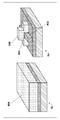
- FIG. 1 is a schematic perspective view showing one typical example of a MOSFET having a three-dimensional structure according to the present invention.
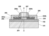
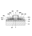
- FIG. 2 is a schematic cross-sectional view taken along line AA shown in FIG.
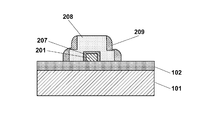
- FIG. 3 is a schematic cross-sectional view taken along line BB shown in FIG.
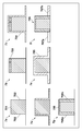
- FIG. 4 is a first schematic process schematic explanatory view showing a pre-process of a process example of a specific manufacturing method of one example of the three-dimensional structure MOS-FET of the present invention.
- FIG. 5 is a second schematic process schematic explanatory view showing an intermediate process of a process example of a specific manufacturing method of one example of the three-dimensional structure MOS-FET of the present invention.
- FIG. 1 is a schematic perspective view showing one typical example of a MOSFET having a three-dimensional structure according to the present invention.
- FIG. 2 is a schematic cross-sectional view taken along line AA shown in FIG.
- FIG. 3 is a schematic cross-sectional view taken along line
- FIG. 6 is a third schematic process schematic explanatory view showing a post-process of a process example of a specific manufacturing method of one example of the three-dimensional structure MOS-FET of the present invention.
- FIG. 7 is a process diagram for schematically explaining one of typical examples of formation of a silicide region according to the present invention.
- FIG. 8 is a process diagram for schematically explaining another typical example of formation of a silicide region according to the present invention.
- FIG. 9 is a schematic cross-sectional view for explaining another typical example of the MOSFET having a three-dimensional structure according to the present invention.
- FIGS. 1, 2 and 3 show one of typical examples of the MOSFET 100 having a three-dimensional structure according to the present invention.
- FIG. 1 is a schematic perspective view
- FIG. 2 is a schematic sectional view taken along line AA shown in FIG. 1
- FIG. 3 is a schematic sectional view taken along line BB shown in FIG.
- the MOSFET 100 includes an SOI layer region 201 in which a channel region (not shown) is formed, and a source region (n + region) 202 and a drain region (n + region) 203 on the outer side of the SOI layer region 201, respectively. Is provided.
- a gate insulating film region 207 and a gate electrode layer region 208 are provided on the upper surface of the SOI layer region 201, respectively.
- Silicide regions 204a and 204b are provided outside the source region 202 and the drain region 203, respectively.
- the source electrode 205 is provided in the silicide region 204a and the drain electrode 206 is provided in direct contact with the silicide region 204b.
- Each of the gate insulating film region 207 and the gate electrode layer region 208 includes not only the upper surface of the SOI layer region 201 but also the SOI layer along the flow direction of the current flowing in the channel region formed in the SOI layer region 201. It also extends to the side surface of the region 201. That is, each of the gate insulating film region 207 and the gate electrode layer region 208 includes the SOI layer region on three surfaces of the outer surface of the SOI layer region 201 along the flow direction of the current flowing in the SOI layer region 201. It is provided so as to surround 201.
- the silicide regions 204a and 204b are side surfaces of the SOI layer region 201, and correspond to two side surfaces that are perpendicular or substantially perpendicular to the flow direction of the current flowing in the SOI layer region 201. It is provided in a state of being in direct electrical contact with the entire side surface or substantially the entire region.
- a channel region formed in the SOI layer region 201 can be formed substantially or substantially in the entire region of the SOI layer region 201.
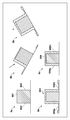
- FIG. 4 is a first schematic process schematic explanatory view showing a pre-process of a process example of a specific manufacturing method of one example of the three-dimensional structure MOS-FET of the present invention
- FIG. 6 is a third schematic process schematic explanatory diagram showing a subsequent process. 4, 5, and 6 explain the process up to the formation of the silicide region 204.
- a preferred example of forming the silicide region 204 on each predetermined crystal plane is shown in FIGS.
- a substrate 400 for forming a three-dimensional structure MOS-FET of the present invention is prepared, and an SOI layer 401 is formed thereon (“Step (4a)” in FIG. 4).
- the base 400 includes a silicon substrate 101 and a BOX layer 102 provided thereon.
- step (4b) the removed portion of the SOI layer 401 is etched by dry etching or the like to form an SOI layer region a402 (“step (4b)” in FIG. 4).
- a gate insulating film (not shown) and a gate electrode layer 404 are formed of an insulating material such as SiO 2 on the SOI layer region a402 by film formation by sputtering and normal patterning.
- the gate electrode layer 404 is made of, for example, Poly-Si (“step (5c)” in FIG. 5).
- step (5d) in FIG. 5).
- Impurities such as boron (B) are ion-implanted at a high concentration in the source / drain formation region of the SOI layer region a402, thereby forming a source region layer 405 and a drain region layer 406 which are high-concentration n + regions.
- Step (6e) in FIG. 6).
- anisotropic etching is performed by dry etching to form sidewalls 209a and 209b as shown in FIG. ) ").
- Step (4a) Preparation of SOI wafer • Adjust the film thickness of the SOI layer as prescribed.
- a gate insulating film is formed of an insulating material such as SiO 2 .
- Step (5d) Etching of the gate electrode, etching of the gate insulating film / Poly-Si for gate electrode (gate electrode layer 404) is dry-etched to form the gate electrode layer region 208.
- the gate insulating film is etched (dry etching or wet etching) to form a gate insulating film region a403.
- Step (6e) Ions are implanted into the source / drain region layer.
- Semiconductor impurities such as boron (B) or phosphorus (P) are ion implanted into the source / drain region layer to form a high concentration region layer (source region layer 405, 405).
- a drain region layer 406) is formed.
- Step (6f) Formation of sidewall 209, deposition of sidewall forming thin film, dry etching (anisotropic etching) of sidewall forming thin film
- a metal layer b705 for forming a silicide is divided into two portions and is provided by an evaporation method as illustrated. At this time, the vapor deposition is carried out by selecting the vapor deposition conditions so as to obtain the optimum thickness of the silicide region on each crystal plane.
- the layer thickness of the metal layer b705 on the (100) plane 702 is thicker than the layer thickness of the metal layer b705 on the (551) plane 701. Therefore, the layer thickness of the silicide region formed by the silicidation process applied later is also thicker on the (100) plane 702.
- the thickness of the silicide region a708 formed on the (551) plane 701 depends on the metal used for silicidation.
- the metal used for silicidation For example, in the case of eurobium (Er), preferably 4 nm The following is desirable.
- a source region 202 and a drain region 203 are formed (see FIG. 2).
- Step (7g) unnecessary metal layers 707a and 707b (unreacted metal layers) that are not silicided are removed by the above silicidation process ("Step (7g)" in FIG. 7).
- a metal for forming an electrical contact is deposited to form a metal layer for forming a contact, and then unnecessary portions of the metal layer are removed by patterning to form a source electrode 205 and a drain electrode 206 ( (See FIG. 2).
- a source / drain region having a three-dimensional structure is formed (step 7a in FIG. 7).
- a resist is applied by a spin coater (step 7b in FIG. 7).
- a metal film is formed to form a metal layer a704 (step 7c in FIG. 7).
- ⁇ Er (Eurobium) is deposited by sputtering. Sputtering conditions: Ar gas flow rate 20 sccm, Pressure: 133 Pa (1 Torr), Film thickness: 8 nm
- Step 7d in FIG. 7 Removal of resist and metal on the resist. For example, the metal film is lifted off while removing the resist with an organic solvent.
- a metal film is formed to form a metal layer b705 (step 7e in FIG. 7).
- ⁇ Er (Eurobium) is deposited by sputtering. Sputtering conditions: Ar gas flow rate 20 sccm, Pressure: 133 Pa (1 Torr), Film thickness: 2 nm
- step 7f in FIG. 7 Silicidation is performed (step 7f in FIG. 7). Lamp annealing is performed at 600 ° C. for 2 minutes.
- a three-dimensional source / drain region is formed (step 8a in FIG. 8).
- a metal layer is formed in the same manner as in FIG. 7 by forming a metal film by tilting the base and performing anisotropic film formation under the following conditions (step 8b in FIG. 8).
- -An Er film is formed by sputtering. Sputtering conditions: Ar gas flow rate 20 sccm, Pressure: 0.67 Pa (5 mTorr), An Er film is formed to 5 nm on the (100) plane and 1 nm on the (551) plane.
- a metal layer is formed by tilting the base and performing anisotropic film formation under the following conditions to form a metal layer as in FIG. 7 (step 8c in FIG. 8).
- Sputtering conditions Ar gas flow rate 20 sccm, Pressure: 0.67 Pa (5 mTorr), An Er film is formed to 5 nm on the (100) plane and 1 nm on the (551) plane.
- an Er film of 10 nm is formed on the (100) plane and 2 nm on the (551) plane.
- a metal (tungsten: W) layer for forming a contact is formed.
- -A tungsten (W) film is formed by sputtering.
- Sputtering conditions Ar gas flow rate ... 20 sccm, Pressure ... 1.33 Pa (10 mTorr), Film thickness ... 100 nm
- FIG. 9 shows an example in which silicide regions are provided on four surfaces of a source / drain region having a three-dimensional structure.
- the example of FIG. 9 is a modification of the example of FIG. That is, in the example of FIG. 2, silicide regions are provided on three surfaces.
- silicide regions 901a and 901b are additionally provided. With such a structure, the current path can be secured more reliably.
Landscapes
- Thin Film Transistor (AREA)
- Electrodes Of Semiconductors (AREA)
- Insulated Gate Type Field-Effect Transistor (AREA)
Abstract
Description
・SOI層の膜厚を所定通りに調整する。
・ドライエッチングで素子分離部のパターン形成
・SiO2などの絶縁材料でゲート絶縁膜を形成する。
・ゲート電極用Poly-Siのデポジッション
・ゲート電極用Poly-Si(ゲート電極層404)をドライエッチング処理して、ゲート電極層領域208を形成する。
・ゲート絶縁膜をエッチング(ドライエッチング又はウェットエッチング)処理して、ゲート絶縁膜領域a403を形成する。
・ソース・ドレイン領域層へボロン(B)又は燐(P)等の半導体不純物をイオン注入して不純物の高濃度領域層(ソース領域層405,ドレイン領域層406)を形成する。
・サイドウォール形成用薄膜のデポジッション
・サイドウォール形成用薄膜をドライエッチング(異方性エッチング)処理
次に、シリサイド領域を設ける例を図7に従って説明する。図7の工程(7c)乃至(7e)において、シリサイド形成用の金属(メタル)層b705を二度に分けて蒸着法により図示のごとく設ける。この際、各結晶面に最適なシリサイド領域の層厚になるように蒸着条件を選択して蒸着する。
・スパッタ法で、Er(ユーロビウム)を成膜する。
・スパッタリング条件:Arガス流量・・・20 sccm,
圧力・・・133 Pa(1 Torr),
膜厚・・・8 nm
例えば、有機溶剤でレジストを剥離しながら、メタル膜をリフトオフする。
・スパッタ法で、Er(ユーロビウム)を成膜する。
・スパッタリング条件:Arガス流量・・・20 sccm,
圧力・・・133 Pa(1 Torr),
膜厚・・・2 nm
600℃で2min間、ランプアニールする。
SPM(H2SO4:H2O2=4:1)を30sec間適用する。
次に、シリサイド領域を設けるもう一つの例を図8に従って説明する。煩雑さを避けるために、以下にまとめ書きして置くことにする。
・スパッタ法でEr膜を形成する。
・スパッタリング条件:Arガスの流量・・・20 sccm,
圧力・・・0.67 Pa(5 mTorr),
・(100)面上に5 nm、(551)面上に1 nm、Er膜を形成する。
・スパッタリング条件:Arガスの流量・・・20 sccm,
圧力・・・0.67 Pa(5 mTorr),
・(100)面上に5 nm、(551)面上に1 nm、Er膜を形成する。
600℃で2min間、ランプアニールする。
SPM(H2SO4:H2O2=4:1)を30sec間適用する。
・スパッタ法に依り、タングステン(W)膜を形成する。
・スパッタリング条件:Arガスの流量・・・・20 sccm,
圧力・・・・1.33 Pa(10 mTorr),
膜厚・・・・100 nm
・Wのドライエッチング条件:Arガスの流量・・・・100 sccm,
SF6ガスの流量・・・・20 sccm,
圧力・・・・1.33 Pa(10 mTorr),
RFパワー・・・・30W
101 シリコン基板
102 BOX層
201 SOI層領域
202 ソース領域
203 ドレイン領域
204 シリサイド領域
205 ソース電極
206 ドレイン電極
207 ゲート絶縁膜領域
208 ゲート電極層領域
209 サイドウォール
400 基体
401 SOI層
402 SOI層領域a
403 ゲート絶縁膜領域a
404 ゲート電極層
405 ソース領域層
406 ドレイン領域層
407 上面ウォール
701 (551)面
702 (100)面
703 レジスト膜
704 メタル層a(シリサイド形成用の金属層)
705 メタル層b(シリサイド形成用の金属層)
706 シリサイド化領域
707 不要(未反応)メタル層
708 シリサイド領域a
709 シリサイド領域
801 (551)面
802 (100)面
803 シリサイド化領域
804 シリサイド領域a
805 シリサイド領域
806 不要(未反応)メタル層
901 シリサイド領域
Claims (2)
- 基本電子素子が3次元構造のMOS-FETであって、それぞれ電極とシリサイド領域を有し、複数の異なる結晶面で構成されているソース領域・ドレイン領域を有する構造を備え、該ソース領域・ドレイン領域のシリサイド領域の層厚が異なる結晶面で異なることを特徴とする半導体装置。
- 基本電子素子が3次元構造のMOS-FETであって、異なる複数の結晶面を有するチャネル領域と、該チャネル領域の複数の結晶面に対面して設けられているゲート電極と、該ゲート電極と前記チャネル領域の間に設けてあるゲート絶縁膜と、前記チャネル領域の電流を流す方向に対面し該チャネル領域を挟むように設けられた第一、第二の半導体不純物の高濃度領域と、を備え、各高濃度領域は、異なる複数の結晶面を有すると共に各結晶面上に直接設けられたシリサイド領域を有し、該シリサイド領域の層厚が異なる結晶面で異なることを特徴とする半導体装置。
Priority Applications (4)
| Application Number | Priority Date | Filing Date | Title |
|---|---|---|---|
| JP2013557317A JP5553256B2 (ja) | 2012-07-09 | 2012-07-09 | 3次元構造のmosfet及びその製造方法 |
| KR1020147019288A KR20140097569A (ko) | 2012-07-09 | 2012-07-09 | 3차원 구조의 mosfet 및 그 제조 방법 |
| PCT/JP2012/004428 WO2014009991A1 (ja) | 2012-07-09 | 2012-07-09 | 3次元構造のmosfet及びその製造方法 |
| US14/285,680 US20140252436A1 (en) | 2012-07-09 | 2014-05-23 | Semiconductor device |
Applications Claiming Priority (1)
| Application Number | Priority Date | Filing Date | Title |
|---|---|---|---|
| PCT/JP2012/004428 WO2014009991A1 (ja) | 2012-07-09 | 2012-07-09 | 3次元構造のmosfet及びその製造方法 |
Related Child Applications (1)
| Application Number | Title | Priority Date | Filing Date |
|---|---|---|---|
| US14/285,680 Continuation US20140252436A1 (en) | 2012-07-09 | 2014-05-23 | Semiconductor device |
Publications (1)
| Publication Number | Publication Date |
|---|---|
| WO2014009991A1 true WO2014009991A1 (ja) | 2014-01-16 |
Family
ID=49915499
Family Applications (1)
| Application Number | Title | Priority Date | Filing Date |
|---|---|---|---|
| PCT/JP2012/004428 Ceased WO2014009991A1 (ja) | 2012-07-09 | 2012-07-09 | 3次元構造のmosfet及びその製造方法 |
Country Status (4)
| Country | Link |
|---|---|
| US (1) | US20140252436A1 (ja) |
| JP (1) | JP5553256B2 (ja) |
| KR (1) | KR20140097569A (ja) |
| WO (1) | WO2014009991A1 (ja) |
Families Citing this family (2)
| Publication number | Priority date | Publication date | Assignee | Title |
|---|---|---|---|---|
| US9209304B2 (en) * | 2014-02-13 | 2015-12-08 | Taiwan Semiconductor Manufacturing Co., Ltd. | N/P MOS FinFET performance enhancement by specific orientation surface |
| US10217819B2 (en) * | 2015-05-20 | 2019-02-26 | Samsung Electronics Co., Ltd. | Semiconductor device including metal-2 dimensional material-semiconductor contact |
Citations (2)
| Publication number | Priority date | Publication date | Assignee | Title |
|---|---|---|---|---|
| JPH03166736A (ja) * | 1989-11-27 | 1991-07-18 | Toshiba Corp | 半導体装置の製造方法 |
| WO2005036651A1 (ja) * | 2003-10-09 | 2005-04-21 | Nec Corporation | 半導体装置及びその製造方法 |
Family Cites Families (5)
| Publication number | Priority date | Publication date | Assignee | Title |
|---|---|---|---|---|
| US7531423B2 (en) * | 2005-12-22 | 2009-05-12 | International Business Machines Corporation | Reduced-resistance finFETs by sidewall silicidation and methods of manufacturing the same |
| US7525160B2 (en) * | 2005-12-27 | 2009-04-28 | Intel Corporation | Multigate device with recessed strain regions |
| JP2009141214A (ja) * | 2007-12-07 | 2009-06-25 | Toshiba Corp | 半導体装置およびその製造方法 |
| JP2011512668A (ja) * | 2008-02-16 | 2011-04-21 | チュンブク ナショナル ユニヴァーシティ インダストリー−アカデミック コーポレイション ファウンデーション | 常温で動作する単電子トランジスタ及びその製造方法 |
| TWI451552B (zh) * | 2009-11-10 | 2014-09-01 | 台灣積體電路製造股份有限公司 | 積體電路結構 |
-
2012
- 2012-07-09 WO PCT/JP2012/004428 patent/WO2014009991A1/ja not_active Ceased
- 2012-07-09 KR KR1020147019288A patent/KR20140097569A/ko not_active Ceased
- 2012-07-09 JP JP2013557317A patent/JP5553256B2/ja active Active
-
2014
- 2014-05-23 US US14/285,680 patent/US20140252436A1/en not_active Abandoned
Patent Citations (2)
| Publication number | Priority date | Publication date | Assignee | Title |
|---|---|---|---|---|
| JPH03166736A (ja) * | 1989-11-27 | 1991-07-18 | Toshiba Corp | 半導体装置の製造方法 |
| WO2005036651A1 (ja) * | 2003-10-09 | 2005-04-21 | Nec Corporation | 半導体装置及びその製造方法 |
Also Published As
| Publication number | Publication date |
|---|---|
| US20140252436A1 (en) | 2014-09-11 |
| JP5553256B2 (ja) | 2014-07-16 |
| KR20140097569A (ko) | 2014-08-06 |
| JPWO2014009991A1 (ja) | 2016-06-20 |
Similar Documents
| Publication | Publication Date | Title |
|---|---|---|
| JP5410666B2 (ja) | 半導体装置 | |
| US7388259B2 (en) | Strained finFET CMOS device structures | |
| CN100378901C (zh) | 应变鳍型场效应晶体管互补金属氧化物半导体器件结构 | |
| TWI390666B (zh) | 絕緣體上半導體裝置之製造方法 | |
| TWI443750B (zh) | 以高效率轉移應力之形成接觸絕緣層之技術 | |
| US7122410B2 (en) | Polysilicon line having a metal silicide region enabling linewidth scaling including forming a second metal silicide region on the substrate | |
| US7781274B2 (en) | Multi-gate field effect transistor and method for manufacturing the same | |
| TW201830578A (zh) | 接觸結構製造方法 | |
| CN103137490B (zh) | 半导体器件及其制造方法 | |
| TWI389200B (zh) | 形成層間介電質之方法 | |
| WO2014063381A1 (zh) | Mosfet的制造方法 | |
| JP2010177690A (ja) | 電気的にプログラムされたソース/ドレイン直列抵抗を有するmosトランジスタ | |
| KR100414735B1 (ko) | 반도체소자 및 그 형성 방법 | |
| WO2013170477A1 (zh) | 半导体器件及其制造方法 | |
| JP5553256B2 (ja) | 3次元構造のmosfet及びその製造方法 | |
| JP2005332993A (ja) | 半導体装置および半導体装置の製造方法 | |
| CN202534635U (zh) | 半导体器件 | |
| WO2014071660A1 (zh) | 半导体器件及其制造方法 | |
| WO2014071666A1 (zh) | 半导体器件及其制造方法 | |
| JP2010141102A (ja) | 半導体装置およびその製造方法 | |
| WO2014009990A1 (ja) | 3次元構造のmosfet及びその製造方法 | |
| CN109887845B (zh) | 半导体器件及其形成方法 | |
| CN102856206B (zh) | 一种半导体结构及其制造方法 | |
| JP2009016754A (ja) | 半導体装置及びその製造方法 | |
| TW201513351A (zh) | 3維構造之mosfet及其製造方法 |
Legal Events
| Date | Code | Title | Description |
|---|---|---|---|
| ENP | Entry into the national phase |
Ref document number: 2013557317 Country of ref document: JP Kind code of ref document: A |
|
| 121 | Ep: the epo has been informed by wipo that ep was designated in this application |
Ref document number: 12880815 Country of ref document: EP Kind code of ref document: A1 |
|
| ENP | Entry into the national phase |
Ref document number: 20147019288 Country of ref document: KR Kind code of ref document: A |
|
| NENP | Non-entry into the national phase |
Ref country code: DE |
|
| 122 | Ep: pct application non-entry in european phase |
Ref document number: 12880815 Country of ref document: EP Kind code of ref document: A1 |