WO2014007416A1 - 박막 태양전지 및 그 제조방법 - Google Patents
박막 태양전지 및 그 제조방법 Download PDFInfo
- Publication number
- WO2014007416A1 WO2014007416A1 PCT/KR2012/005457 KR2012005457W WO2014007416A1 WO 2014007416 A1 WO2014007416 A1 WO 2014007416A1 KR 2012005457 W KR2012005457 W KR 2012005457W WO 2014007416 A1 WO2014007416 A1 WO 2014007416A1
- Authority
- WO
- WIPO (PCT)
- Prior art keywords
- electrode layer
- layer
- thin film
- solar cell
- film solar
- Prior art date
- Legal status (The legal status is an assumption and is not a legal conclusion. Google has not performed a legal analysis and makes no representation as to the accuracy of the status listed.)
- Ceased
Links
Images



Classifications
-
- H—ELECTRICITY
- H10—SEMICONDUCTOR DEVICES; ELECTRIC SOLID-STATE DEVICES NOT OTHERWISE PROVIDED FOR
- H10F—INORGANIC SEMICONDUCTOR DEVICES SENSITIVE TO INFRARED RADIATION, LIGHT, ELECTROMAGNETIC RADIATION OF SHORTER WAVELENGTH OR CORPUSCULAR RADIATION
- H10F19/00—Integrated devices, or assemblies of multiple devices, comprising at least one photovoltaic cell covered by group H10F10/00, e.g. photovoltaic modules
- H10F19/30—Integrated devices, or assemblies of multiple devices, comprising at least one photovoltaic cell covered by group H10F10/00, e.g. photovoltaic modules comprising thin-film photovoltaic cells
-
- H—ELECTRICITY
- H10—SEMICONDUCTOR DEVICES; ELECTRIC SOLID-STATE DEVICES NOT OTHERWISE PROVIDED FOR
- H10F—INORGANIC SEMICONDUCTOR DEVICES SENSITIVE TO INFRARED RADIATION, LIGHT, ELECTROMAGNETIC RADIATION OF SHORTER WAVELENGTH OR CORPUSCULAR RADIATION
- H10F10/00—Individual photovoltaic cells, e.g. solar cells
- H10F10/10—Individual photovoltaic cells, e.g. solar cells having potential barriers
- H10F10/12—Photovoltaic cells having only metal-insulator-semiconductor [MIS] potential barriers
-
- H—ELECTRICITY
- H10—SEMICONDUCTOR DEVICES; ELECTRIC SOLID-STATE DEVICES NOT OTHERWISE PROVIDED FOR
- H10F—INORGANIC SEMICONDUCTOR DEVICES SENSITIVE TO INFRARED RADIATION, LIGHT, ELECTROMAGNETIC RADIATION OF SHORTER WAVELENGTH OR CORPUSCULAR RADIATION
- H10F10/00—Individual photovoltaic cells, e.g. solar cells
- H10F10/10—Individual photovoltaic cells, e.g. solar cells having potential barriers
- H10F10/17—Photovoltaic cells having only PIN junction potential barriers
-
- H—ELECTRICITY
- H10—SEMICONDUCTOR DEVICES; ELECTRIC SOLID-STATE DEVICES NOT OTHERWISE PROVIDED FOR
- H10F—INORGANIC SEMICONDUCTOR DEVICES SENSITIVE TO INFRARED RADIATION, LIGHT, ELECTROMAGNETIC RADIATION OF SHORTER WAVELENGTH OR CORPUSCULAR RADIATION
- H10F10/00—Individual photovoltaic cells, e.g. solar cells
- H10F10/10—Individual photovoltaic cells, e.g. solar cells having potential barriers
- H10F10/18—Photovoltaic cells having only Schottky potential barriers
-
- H—ELECTRICITY
- H10—SEMICONDUCTOR DEVICES; ELECTRIC SOLID-STATE DEVICES NOT OTHERWISE PROVIDED FOR
- H10F—INORGANIC SEMICONDUCTOR DEVICES SENSITIVE TO INFRARED RADIATION, LIGHT, ELECTROMAGNETIC RADIATION OF SHORTER WAVELENGTH OR CORPUSCULAR RADIATION
- H10F10/00—Individual photovoltaic cells, e.g. solar cells
- H10F10/10—Individual photovoltaic cells, e.g. solar cells having potential barriers
- H10F10/19—Photovoltaic cells having multiple potential barriers of different types, e.g. tandem cells having both PN and PIN junctions
-
- H—ELECTRICITY
- H10—SEMICONDUCTOR DEVICES; ELECTRIC SOLID-STATE DEVICES NOT OTHERWISE PROVIDED FOR
- H10F—INORGANIC SEMICONDUCTOR DEVICES SENSITIVE TO INFRARED RADIATION, LIGHT, ELECTROMAGNETIC RADIATION OF SHORTER WAVELENGTH OR CORPUSCULAR RADIATION
- H10F71/00—Manufacture or treatment of devices covered by this subclass
-
- H—ELECTRICITY
- H10—SEMICONDUCTOR DEVICES; ELECTRIC SOLID-STATE DEVICES NOT OTHERWISE PROVIDED FOR
- H10F—INORGANIC SEMICONDUCTOR DEVICES SENSITIVE TO INFRARED RADIATION, LIGHT, ELECTROMAGNETIC RADIATION OF SHORTER WAVELENGTH OR CORPUSCULAR RADIATION
- H10F71/00—Manufacture or treatment of devices covered by this subclass
- H10F71/121—The active layers comprising only Group IV materials
-
- H—ELECTRICITY
- H10—SEMICONDUCTOR DEVICES; ELECTRIC SOLID-STATE DEVICES NOT OTHERWISE PROVIDED FOR
- H10F—INORGANIC SEMICONDUCTOR DEVICES SENSITIVE TO INFRARED RADIATION, LIGHT, ELECTROMAGNETIC RADIATION OF SHORTER WAVELENGTH OR CORPUSCULAR RADIATION
- H10F77/00—Constructional details of devices covered by this subclass
- H10F77/20—Electrodes
-
- Y—GENERAL TAGGING OF NEW TECHNOLOGICAL DEVELOPMENTS; GENERAL TAGGING OF CROSS-SECTIONAL TECHNOLOGIES SPANNING OVER SEVERAL SECTIONS OF THE IPC; TECHNICAL SUBJECTS COVERED BY FORMER USPC CROSS-REFERENCE ART COLLECTIONS [XRACs] AND DIGESTS
- Y02—TECHNOLOGIES OR APPLICATIONS FOR MITIGATION OR ADAPTATION AGAINST CLIMATE CHANGE
- Y02E—REDUCTION OF GREENHOUSE GAS [GHG] EMISSIONS, RELATED TO ENERGY GENERATION, TRANSMISSION OR DISTRIBUTION
- Y02E10/00—Energy generation through renewable energy sources
- Y02E10/50—Photovoltaic [PV] energy
- Y02E10/547—Monocrystalline silicon PV cells
-
- Y—GENERAL TAGGING OF NEW TECHNOLOGICAL DEVELOPMENTS; GENERAL TAGGING OF CROSS-SECTIONAL TECHNOLOGIES SPANNING OVER SEVERAL SECTIONS OF THE IPC; TECHNICAL SUBJECTS COVERED BY FORMER USPC CROSS-REFERENCE ART COLLECTIONS [XRACs] AND DIGESTS
- Y02—TECHNOLOGIES OR APPLICATIONS FOR MITIGATION OR ADAPTATION AGAINST CLIMATE CHANGE
- Y02E—REDUCTION OF GREENHOUSE GAS [GHG] EMISSIONS, RELATED TO ENERGY GENERATION, TRANSMISSION OR DISTRIBUTION
- Y02E10/00—Energy generation through renewable energy sources
- Y02E10/50—Photovoltaic [PV] energy
- Y02E10/548—Amorphous silicon PV cells
-
- Y—GENERAL TAGGING OF NEW TECHNOLOGICAL DEVELOPMENTS; GENERAL TAGGING OF CROSS-SECTIONAL TECHNOLOGIES SPANNING OVER SEVERAL SECTIONS OF THE IPC; TECHNICAL SUBJECTS COVERED BY FORMER USPC CROSS-REFERENCE ART COLLECTIONS [XRACs] AND DIGESTS
- Y02—TECHNOLOGIES OR APPLICATIONS FOR MITIGATION OR ADAPTATION AGAINST CLIMATE CHANGE
- Y02P—CLIMATE CHANGE MITIGATION TECHNOLOGIES IN THE PRODUCTION OR PROCESSING OF GOODS
- Y02P70/00—Climate change mitigation technologies in the production process for final industrial or consumer products
- Y02P70/50—Manufacturing or production processes characterised by the final manufactured product
Definitions
- the present invention relates to a solar cell, and more particularly to a thin film solar cell.
- Thin film solar cells can be classified into various types according to the deposition temperature of the thin film, the type of substrate used, and the deposition method.
- the amorphous and crystalline silicon thin film solar cells are largely classified according to the crystal characteristics of the intrinsic layer. Can be classified as a battery.
- Thin film solar cell uses thin film as light absorbing layer, and its light absorption coefficient is much higher than that of crystalline silicon solar cell, and it is possible to use inexpensive substrate such as glass or metal plate instead of expensive silicon substrate. It has the advantage of being low. In addition, since it can be based on LCD production technology, the initial capital investment cost can be significantly lowered, and since the low temperature process is possible, the device can be implemented using a flexible substrate.
- FIG. 1 is a cross-sectional view schematically showing the structure of a conventional thin film solar cell.
- FIG. 1 illustrates a structure of a pin super-straight type thin film solar cell.
- a TCO layer 11 and a p-type semiconductor layer 12 and a- are disposed on a substrate 10 on which light is incident.
- the i-type semiconductor layer 13 a-Si: H
- the n-type semiconductor layer 14 a-Si: H
- the back electrode 15 are sequentially formed.
- the i-type semiconductor layer 13 which is an intrinsic semiconductor to which no impurities are added, is placed between the p-type semiconductor layer 12 and the n-type semiconductor layer 14 having a high doping concentration. It has an inserted shape, which is commonly referred to as a pin structure.
- the i-type semiconductor layer 13 is depleted by the p-type semiconductor layer 12 and the n-type semiconductor layer 14 having a high doping concentration, and thus the incident light is emitted from the i-type semiconductor layer 13.
- the generated electron-hole pairs are collected at each interface by drift by an internal electric field to generate current.
- the above-described thin film solar cell having a p-i-n structure has the following problems. First, since light stability is relatively low due to an increase in defects caused by doping layers such as a p-type semiconductor layer and an n-type semiconductor layer, degradation is caused when exposed to light. The phenomenon occurred.
- a toxic gas is generated in the process process may cause workers to be exposed to the harmful gas may adversely affect the working environment. have.
- the pin layers are all deposited by using PECVD (Plasma Enhanced Chemical Vapor Depostion) using SiH 4 and H 2 gas, and the PECVD is performed by thermal evaporation or sputtering.
- PECVD Pulsma Enhanced Chemical Vapor Depostion
- SiH 4 and H 2 gas SiH 4 and H 2 gas
- the PECVD is performed by thermal evaporation or sputtering.
- the thin film solar cell having a pin structure uses doping layers such as a p-type semiconductor layer and an n-type semiconductor layer, and uses the p-type semiconductor layer and / or the n-type semiconductor layer as the doping layer. Attempts have been made to remove or replace with other materials.
- Non-Patent Document 1 a study has recently been disclosed in which an n-type semiconductor layer is replaced with a LiF / Al Schottky junction in a p-i-n structure. The study describes that the efficiency characteristics of the solar cell can be realized at an appropriate level even though a part of the doping layer is removed by replacing the n-type semiconductor layer with a LiF / Al Schottky junction.
- Embodiments of the present invention provide a thin film solar cell and a method of manufacturing the same without doping layers (p-type semiconductor layer and n-type semiconductor layer).
- the substrate; A front electrode layer formed on the substrate; An oxide layer formed on the front electrode; An intrinsic layer formed on the oxide layer; And a back electrode layer formed on the light absorbing layer, and the oxide layer may be provided with a thin film solar cell formed of a material selected from MoO 3, WO 3, V 2 O 5, and CrO 3.
- the thickness of the oxide layer may be 1nm to 30nm.
- the back electrode layer may include a first electrode layer formed on the light absorbing layer and a second electrode layer formed on the first electrode layer, and the first electrode layer may include LiF, Liq, CsCl, ZrO 2 , and Al 2. It is formed of a material selected from O 3 and SiO 2 , the second electrode layer may be formed of a material selected from Al, Ag, Mg, Ca and Li.
- the first electrode layer may be formed of LiF
- the second electrode layer may be formed of Al
- the thickness of the first electrode layer may be 0.1nm to 2.0nm.
- the substrate may be a glass substrate coated with Fluorine Tin Oxide (FTO).
- FTO Fluorine Tin Oxide
- the front electrode layer is selected from the group consisting of Fluorine Tin Oxide (FTO), Indium Tin Oxide (ITO), ZnO: Al, AgO, and mixtures thereof, or may be formed of a double layer consisting of ITO / GZO or ZnO / AZO. Can be.
- the light absorbing layer may be an amorphous silicon thin film (a-Si: H), a microcrystalline silicon thin film (Micro-Crystalline Silicon, mc-Si: H), a crystalline silicon thin film (Crystalline Silicon, Si: H), a polycrystalline silicon thin film. (Polycrystalline Silicon, pc-Si: H) and nano-crystalline silicon (Nano-Crystalline Silicon, nc-Si: H) may be selected.
- the oxide layer is formed by a thermal evaporation (thermal evaporation), sputtering (sputtering) process or electron beam evaporation (E-beam evaporation) It can be provided a method for manufacturing a thin film solar cell made using).
- the back electrode layer is formed including a first electrode layer formed on the light absorbing layer and a second electrode layer formed on the first electrode layer, and the oxide layer and the back electrode layer are formed using the thermal vapor deposition method.
- the oxide layer may be formed to have a thickness of 10 nm to 30 nm, and the first electrode layer may have a thickness of 1.0 nm to 2.0 nm.
- the rear electrode layer may include a first electrode layer formed on the light absorbing layer and a second electrode layer formed on the first electrode layer, and the oxide layer may be formed using the sputtering process.
- the electrode layer may be formed using the thermal evaporation method.
- the oxide layer may have a thickness of 5 nm to 10 nm, and the first electrode layer may have a thickness of 1.0 nm to 2.0 nm.
- Embodiments of the present invention implemented a thin film solar cell without doping layers by replacing the p-type semiconductor layer with an oxide layer and the n-type semiconductor layer with a back electrode layer composed of LiF / Al in the conventional pin structure thin film solar cell. .
- FIG. 1 is a cross-sectional view schematically showing the structure of a conventional thin film solar cell.
- FIG. 2 is a cross-sectional view schematically showing the structure of a thin film solar cell according to an embodiment of the present invention.
- FIG. 3 is a graph showing current density-voltage (I-V) characteristics of Comparative Example 1 and Examples 1 to 3.
- I-V current density-voltage
- FIG. 4 is a graph showing current density-voltage (I-V) characteristics in the dark room of Comparative Example 2 and Examples 4 to 9.
- I-V current density-voltage
- FIG. 5 is a graph showing current density-voltage (I-V) characteristics of Comparative Example 2 and Examples 4 to 9.
- I-V current density-voltage
- FIG. 7 is a graph illustrating current density-voltage (I-V) characteristics of Examples 14 to 17.
- FIG. 7 is a graph illustrating current density-voltage (I-V) characteristics of Examples 14 to 17.
- n-type semiconductor layer 15 back electrode
- substrate 120 front electrode layer
- oxide layer 140 light absorbing layer
- the expression “upper”, “on” or “on” is used to refer to the concept of relative position with reference to the accompanying drawings, and the above expressions may directly exist with other components or layers in the layer mentioned.
- other layers or components may be interposed or present therebetween, and also completely above the surface of the mentioned layer (in particular, having a three-dimensional shape), which is present at the top in relation to the mentioned layer. Note that it may also include uncovered cases.
- the expression “bottom”, “bottom” or “below” may also be understood as a relative concept of the position between a particular layer (component) and another layer (component).
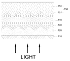
- FIG. 2 is a cross-sectional view schematically showing the structure of a thin film solar cell 100 (hereinafter referred to as a thin film solar cell) according to an embodiment of the present invention.
- the thin film solar cell 100 may include a structure in which the front electrode layer 120, the oxide layer 130, the light absorbing layer 140, and the rear electrode layer 150 are sequentially formed on the substrate 110. Can be.
- a plurality of irregularities having an amorphous pyramid structure may be formed on one or both surfaces of the substrate 110, the front electrode layer 120, the oxide layer 130, the light absorbing layer 140, and the rear electrode layer 150. That is, the configurations can have a texturing surface.
- the texturing surface may contribute to improving the efficiency of the solar cell by reducing the reflectivity of the incident light and increasing the movement path inside the light absorbing layer 1450 due to scattering of the incident light. 2 shows a thin film solar cell 100 with a textured surface.
- the substrate 110 may be formed of a transparent material so that incident light effectively reaches the light absorbing layer 140. That is, the substrate 110 may be a glass substrate or a transparent plastic substrate. Examples of such a substrate 110 include a glass substrate coated with Fluorine Tin Oxide (FTO), a substrate coated with Indium Tin Oxide (ITO), and a substrate coated with Gallium Zinc Oxide (GZO), or AZO ( Aluminum zinc oxide may be coated with a substrate, but is not limited thereto.
- FTO Fluorine Tin Oxide
- ITO Indium Tin Oxide
- GZO Gallium Zinc Oxide
- AZO Aluminum zinc oxide may be coated with a substrate, but is not limited thereto.
- the FTO may function as the front electrode layer 120.
- the front electrode layer 120 collects and outputs one of the carriers generated by the incident light (for example, holes), and the front electrode layer 120 is formed of a transparent material and a material having electrical conductivity to increase the transmittance of the incident light. Can be.
- the front electrode layer 120 may be formed of tin oxide (SnO 2 , SnO 2 : F, ITO), gallium zinc oxide (ITO / GZO) or ZnO / AZO, double layer (ZnO: Al, AgO). And it can be selected from the group consisting of a mixture thereof.
- the oxide layer 130 is formed on the front electrode layer 120.
- the p-type semiconductor layer which is one of the doping layers in the conventional thin film solar cell, is illustrated in FIG. ) Is replaced with an oxide layer 130 formed of a material selected from MoO 3 (Molybdenum oxide), WO 3 (Tungsten oxide), V 2 O 5 (Vanadium oxide) and CrO 3 (Chromium oxide) do.
- MoO 3 Molybdenum oxide
- WO 3 Teungsten oxide
- V 2 O 5 Vehicle oxide
- CrO 3 Chromium oxide
- MoO 3 has a high electrical conductivity and a wide optical bandgap (3.16 eV), which corresponds to a material satisfying the above-mentioned conditions.
- the inventors of the present invention have the advantage that the above-described oxide materials such as MoO 3 are not doped layers, unlike the p-type semiconductor layers, and thus can solve the problems caused by the doping layer while replacing the p-type semiconductor layers. It was confirmed.
- the doping layer is replaced with an oxide material, defects caused by the doping layer do not occur, and in the case of MoO 3 material, it can function as a capping layer on the front side of the light absorption layer. It can improve stability.
- PECVD Pulsma Enhanced Chemical Vapor Depostio
- the thickness of the oxide layer 130 is not particularly limited, but is preferably formed to a thickness of 1 nm to 30 nm. When the thickness of the oxide layer 130 is less than 1 nm or more than 30 nm, efficiency characteristics of the thin film solar cell 100 of the present invention may not be sufficiently implemented. This will be supplemented in a test example to be described later.
- the light absorbing layer 140 is formed on the oxide layer 130, and receives an incident light to generate an electron-hole pair to generate a current.
- an amorphous silicon thin film (a-Si: H), a microcrystalline silicon thin film (Micro-Crystalline Silicon, mc-Si: H), a crystalline silicon thin film (Crystalline Silicon, Si: H), polycrystalline silicon A thin film (Polycrystalline Silicon, pc-Si: H) or a nano-crystalline silicon (Nano-Crystalline Silicon, nc-Si: H) may be used, but is not limited thereto.
- the light absorbing layer 140 will be described based on an amorphous silicon thin film.
- the thickness of the light absorbing layer 140 is not limited and may be, for example, formed to a thickness of 50nm to 1000nm.
- the back electrode layer 150 is formed on the light absorbing layer 140 and may include a first electrode layer 151 formed on the light absorbing layer and a second electrode layer 152 formed on the first electrode layer 151. have.
- the first electrode layer 151 may be formed of a material selected from LiF, Liq, CsCl, ZrO 2 , Al 2 O 3, and SiO 2 , but is not limited thereto.
- the second electrode layer 152 may be formed of a material selected from Al, Ag, Mg, Ca, and Li, but is not limited thereto.
- the combination of the first electrode layer 151 and the second electrode layer 152 may include LiF / Al, ZrO 2 / Al, ZrO 2 / Ag, ZrO 2 / Mg, ZrO 2 / Ca, ZrO 2 / Li, Al 2 O 3 / Al, Al 2 O 3 / Ag, SiO 2 / Al or SiO 2 / Ag, and the like, but are not limited thereto.
- the n-type semiconductor layer (see FIG. 1), which is one of the doping layers, is removed from the conventional thin film solar cell, and the first electrode layer 151 / the second electrode layer ( 152 is replaced by a back electrode layer 150 formed.
- the first electrode layer 151 is LiF
- the second electrode layer 152 will be described based on the case where LiF / Al, which is Al, is used as the back electrode layer 150.
- the first electrode layer 151 and the second electrode layer 152 are Schottky junctions, and may replace the n-type semiconductor layer in the thin film solar cell. This is described in detail in [Non-Patent Document] (Liang Fang et al, IEEE TRANSCATIONS ON ELECTRON DEVICES, VOL. 58, NO. 9, SEPTEMBER 2011, pp. 3048-3051), and the present specification is described in the non-patent document. Note that it may contain
- the first electrode layer 151 may function as surface passivation, and the thickness of the first electrode layer 151 is not particularly limited, but is preferably formed to a thickness of 0.1 nm to 2.0 nm. When the thickness of the first electrode layer 151 is outside the above range, the efficiency characteristic of the thin film solar cell 100 of the present invention may not be sufficiently implemented. This will be supplemented in a test example to be described later.
- the second electrode layer 152 may collect and output one of the carriers generated by the incident light (for example, electrons).
- the front electrode layer 120 is formed on the substrate 110 or an FTO glass coated with FTO is prepared.
- the front electrode layer 120 is made of tin oxide (SnO 2 , SnO 2 : F, ITO), gallium zinc oxide (ITO / GZO) or ZnO / AZO double layer, ZnO: Al, AgO and mixtures thereof Materials selected from the group consisting of can be used.
- the oxide layer 130 is deposited on the front electrode layer 120.
- the oxide layer 130 may be formed of a material selected from among molybdenum oxide (MoO 3 ), tungsten oxide (WO 3 ), vanadium oxide (V 2 O 5 ), and chromium oxide (CrO 3 ).
- a thermal evaporation method, a sputtering process, or an electron beam evaporation process may be used as a deposition method under a low 10 ⁇ 6 Torr vacuum condition.
- an amorphous silicon thin film (a-Si: H), a microcrystalline silicon thin film (Micro-Crystalline Silicon, mc-Si: H), a crystalline silicon thin film (Crystalline Silicon, Si: H), PECVD process, Photo-CVD, Lase CVD or sputtering the light absorbing layer 140 made of polycrystalline silicon (pc-Si: H) or nanocrystalline silicon thin film (Nano-Crystalline Silicon, nc-Si: H)
- the second electrode layer 152 formed of a material selected from Mg, Ca, and Li may be formed by a thermal evaporation method or a sputtering process to manufacture a thin film solar cell.
- the doping layers such as the p-type semiconductor layer and the n-type semiconductor layer were deposited by using a PECVD process
- the oxide layer 130 and the back electrode layer 150 which are not the doping layer
- the overall process cost can be reduced.
- the doping layer does not need to be formed, there is no harmful gas generated when the doping layer is formed, thereby making it possible to manufacture a thin film solar cell.
- the embodiments of the present invention replace the p-type semiconductor layer with an oxide layer formed of a material selected from MoO 3 , WO 3 , V 2 O 5 and CrO 3 in a conventional pin structure thin film solar cell
- the n-type semiconductor layer is a first electrode layer formed of a material selected from LiF, Liq, CsCl, ZrO 2 , Al 2 O 3 and SiO 2 and a second formed of a material selected from Al, Ag, Mg, Ca and Li
- test example of the present invention will be described. However, it is obvious that the following test examples do not limit the present invention.
- Comparative Examples and Examples can be divided into the presence or absence of an oxide layer, specifically, Comparative Example is to remove the p-type semiconductor layer from a conventional thin film solar cell, Example is a p-type semiconductor layer It is replaced by an oxide layer. At this time, MoO 3 was used as the oxide layer, and thermal evaporation was used as a method of forming the oxide layer.
- Comparative Examples 1 and 2 were different in the thickness of the LiF, the examples were different in the thickness of the oxide layer (MoO 3 ) and LiF.
- Comparative Example 3 Examples 10 to 13 are the same for all the configurations except for Comparative Example 2, Examples 6 to 9 and FTO glass of the above [Table 1].
- thin film solar cells corresponding to Examples 14 to 17 were produced, which are summarized in the following [Table 3].
- FTO glass Pankington glass, Inc.
- the light absorbing material was formed to a thickness of 450 nm using a-Si: H.
- MoO 3 was used as the oxide layer, and the sputtering process was used as a method of forming the oxide layer, unlike Examples 1 to 9.
- the n-type semiconductor layer was replaced with a LiF / Al back electrode layer in the conventional thin film solar cell, and thermal deposition was used as a method of forming the back electrode layer.
- the thickness of the LiF was 1.4nm
- the thickness of the oxide layer (MoO 3 ) was varied. This is summarized in the following [Table 3].
- Example 14 FTO / MoO 3 (3nm) / a-Si: H (450nm) / LiF (1.4nm) / Al Note: A sputtering process is used to form the oxide layer.
- Example 15 FTO / MoO 3 (5nm) / a-Si: H (450nm) / LiF (1.4nm) / Al
- Example 16 FTO / MoO 3 (7.5nm) / a-Si: H (450nm) / LiF (1.4nm) / Al
- Example 17 FTO / MoO 3 (10nm) / a-Si: H (450nm) / LiF (1.4nm) / Al
- Example 1 15.59 0.29 0.53 2.48 Comparative Example 2 14.97 0.31 0.50 2.35 Comparative Example 3 15.58 0.38 0.53 3.21 Example 1 14.62 0.34 0.55 2.79 Example 2 15.11 0.46 0.60 4.24 Example 3 15.23 0.53 0.63 5.20 Example 4 14.88 0.47 0.60 4.23 Example 5 15.39 0.61 0.58 5.53 Example 6 15.27 0.66 0.64 6.55 Example 7 14.66 0.72 0.65 6.98 Example 8 14.99 0.65 0.64 6.36 Example 9 13.99 0.67 0.64 6.07 Example 10 16.65 0.68 0.62 7.06 Example 11 15.65 0.68 0.62 6.71 Example 12 14.72 0.69 0.62 6.45 Example 13 14.50 0.67 0.61 6.02 Example 14 15.88 0.49 0.62 4.87 Example 15 16.32 0.62 0.66 6.59 Example 16 16.08 0.65 0.67 7.08 Example 17 14.27 0.66 0.68 6.43
- LiF thickness is 0.7 nm
- FIG. 3 is a graph showing current density-voltage (I-V) characteristics of Comparative Example 1 and Examples 1 to 3.
- FIG. Comparative Examples 1 and 1 to 3 were formed such that LiF had a thickness of 0.7 nm.
- FIG. 4 is a graph showing current density-voltage (IV) characteristics in the dark room of Comparative Example 2 and Examples 4 to 9, and FIG. 5 is a graph of current density-voltage (IV) characteristics of Comparative Example 2 and Examples 4 to 9 .
- Comparative Example 2 and Examples 4 to 9 were formed such that LiF had a thickness of 1.4 nm.
- Example 16 in which the oxide layer was formed using a sputtering process, it was confirmed that the light stability was superior to Comparative Example 2 and the thin film solar cell (reference) having the conventional p-i-n structure. This shows that since the oxide layer formed by the sputtering process is more dense than the thin film formed by the thermal evaporation method, a thin film thickness can be formed while securing the same level of light stability, thereby lowering the manufacturing cost.
- FIG. 7 is a graph of current density-voltage (IV) characteristics of Examples 14 to 17.
- FIG. 7 in the case where an oxide layer (MoO 3 ) is present as in the previous test result, the open voltage (V oc ), the Fill Factor, and the non-existing case (see Comparative Examples 2 and 3 in Table 4) are not present. It can be seen that the efficiency is improved.
- the maximum efficiency was measured to be 7.08% when the thickness of the oxide layer was 7.5 nm (Example 16). This is different from that in which the maximum efficiency is measured when the thickness of the oxide layer is 20 nm when using the thermal evaporation method (Example 7), and it can be confirmed that a suitable oxide layer thickness is derived according to the formation process of the oxide layer. have. However, in any case, it was confirmed that higher efficiency can be achieved than when the oxide layer (MoO 3 ) does not exist (Comparative Examples 1, 2 and 3).
- the reason why the thickness of the oxide layer formed by the sputtering process is smaller than that of the oxide layer formed by the thermal evaporation method is that it is denser than the thin film formed by the thermal evaporation method formed by the sputtering process. Therefore, in the case of forming the oxide layer by the sputtering process, it is possible to reduce the manufacturing cost since the same level of efficiency can be ensured while the film thickness is thinner than the case of the thermal evaporation method.
- the inventors of the present invention derive the optimum thickness of the oxide in the most mass-produced sputtering process in terms of film uniformity and process stability in a large area substrate using a semiconductor process as described above, which greatly improves the productivity of thin film solar cells. You can.
Landscapes
- Photovoltaic Devices (AREA)
- Engineering & Computer Science (AREA)
- Manufacturing & Machinery (AREA)
Description
본 발명은 태양전지에 관한 것으로, 보다 상세하게는 박막 태양전지에 관한 것이다.
박막 태양전지는 박막 증착온도, 사용되는 기판의 종류 및 증착방법에 따라 다양하게 분류될 수 있는데, 광 흡수층(intrinsic layer)의 결정특성에 따라서는 크게 비정질(amorphous)과 결정질(crystalline) 실리콘 박막 태양전지로 분류될 수 있다.
박막 태양전지는 광 흡수층으로 박막을 이용하는 것으로, 광흡수계수가 결정질 실리콘 태양전지에 비하여 크게 높고, 고가의 실리콘 기판대신 유리나 금속판과 같은 저가의 기판을 사용할 수 있어 기판 소재비가 결정계 태양전지에 비해 매우 낮다는 장점이 있다. 또한, LCD 생산기술을 기반할 수 있으므로 초기설비 투자비를 크게 낮출 수 있고, 저온공정이 가능하여 플렉서블 기판을 이용한 소자 구현이 가능하다는 장점이 있으므로 최근 많은 연구 개발이 이루어지고 있다.
도 1은 종래 박막 태양전지의 구조를 개략적으로 도시한 단면도이다.
도 1에서는 p-i-n 슈퍼스트레이트형 박막 태양전지의 구조를 도시하고 있는데, 이와 같은 구조의 종래 박막 태양전지는 광이 입사되는 기판(10)위에 TCO층(11), p형 반도체층(12, a-Si:H), i형 반도체층(13, a-Si:H), n형 반도체층(14, a-Si:H) 및 후면 전극(15)이 순차적으로 증착되어 구성된다.
보다 구체적으로, 종래 박막 태양전지는 불순물이 첨가되지 않은 진성(intrinsic) 반도체인 i형 반도체층(13)을 높은 도핑 농도를 갖는 p형 반도체층(12) 및 n형 반도체층(14) 중간에 삽입된 형태를 가지며, 이를 통상적으로 p-i-n 구조라고 한다. 이러한 구조에서는 i형 반도체층(13)은 높은 도핑 농도를 갖는 p형 반도체층(12) 및 n형 반도체층(14)에 의해 공핍(depletion)되며, 따라서 i형 반도체층(13)에서 입사광에 의해 생성된 전자-정공쌍(electron-hole pairs)은 내부 전기장에 의한 드리프트에 의해 각 계면에 수집됨으로써 전류를 발생하게 된다.
그런데, 상술한 p-i-n 구조를 갖는 박막 태양전지는 다음과 같은 문제가 있었다. 첫째, p형 반도체층 및 n형 반도체층과 같은 도핑 레이어(doping layer)들에 의한 결함(defect) 증가로 광안정성(light stability)이 상대적으로 낮으므로, 빛에 노출될 경우에 열화(degradation) 현상이 발생하였다.
둘째, p형 반도체층 및 n형 반도체층은 높은 도핑 농도를 갖도록 형성되므로, 공정 과정에서 유해 가스(toxic gas)가 발생하여 작업자가 상기 유해 가스에 노출될 우려가 있어 작업 환경에 악영향을 미칠 수 있다.
셋째, p-i-n층은 모두 SiH4 및 H2 가스를 이용한 PECVD(플라즈마 화학기상증착공정, Plasma Enhanced Chemical Vapor Depostion)를 이용하여 증착되는데, 상기 PECVD는 열 증착(thermal evaporation) 또는 스퍼터링(sputtering) 공정과 비교하여 공정비용 및 초기설비투자비가 증가하는 문제가 있다.
상술한 문제점들은 모두 p-i-n 구조의 박막 태양전지가 p형 반도체층 및 n형 반도체층과 같은 도핑 레이어들을 사용하고 있기 때문에 발생하는 것으로, 상기 도핑 레이어인 p형 반도체층 및/또는 n형 반도체층을 제거 또는 다른 물질로 대체하는 시도가 이루어지고 있다.
관련하여, 최근에 p-i-n 구조에서 n형 반도체층을 LiF/Al 쇼트키 접합으로 대체한 연구가 개시된 바 있다(비특허 문헌 1). 상기 연구에서는 n형 반도체층을 LiF/Al 쇼트키 접합으로 대체하여 도핑 레이어의 일부를 제거하였음에도 태양전지의 효율 특성이 적정한 수준으로 구현될 수 있음을 기재하고 있다.
그러나, 상기 연구에서는 여전히 도핑 레이어로써 p형 반도체층이 존재하고 있으므로, 도핑 레이어들에 의한 상기 문제점들이 완전히 해결되지는 않는다. 후속 연구가 필요한 이유이다.
본 발명의 실시예들은 도핑 레이어들(p형 반도체층 및 n형 반도체층)이 없는 박막 태양전지 및 그 제조방법을 제공하고자 한다.
본 발명의 일 측면에 따르면, 기판; 상기 기판상에 형성되는 전면 전극층; 상기 전면 전극 상에 형성되는 옥사이드층; 상기 옥사이드층 상에 형성되는 광 흡수층(intrinsic layer); 및 상기 광 흡수층 상에 형성되는 후면 전극층을 포함하고, 상기 옥사이드층은 MoO3, WO3, V2O5 및 CrO3 중에서 선택되는 물질로 형성되는 박막 태양전지가 제공될 수 있다.
이 때, 상기 옥사이드층의 두께는 1nm 내지 30nm일 수 있다.
또한, 상기 후면 전극층은, 상기 광 흡수층 상에 형성되는 제1 전극층과, 상기 제1 전극층 상에 형성되는 제2 전극층을 포함하고, 상기 제1 전극층은 LiF, Liq, CsCl, ZrO2, Al2O3 및 SiO2 중에서 선택되는 물질로 형성되고, 상기 제2 전극층은 Al, Ag, Mg, Ca 및 Li 중에서 선택되는 물질로 형성될 수 있다.
이 때, 상기 제1 전극층은 LiF로 형성되고, 상기 제2 전극층은 Al로 형성될 수 있다.
또한, 상기 제1 전극층의 두께는 0.1nm 내지 2.0nm일 수 있다.
한편, 상기 기판은 FTO(Fluorine Tin Oxide)가 코팅된 유리 기판일 수 있다.
또한, 상기 전면 전극층은, FTO(Fluorine Tin Oxide), ITO(Indium Tin Oxide), ZnO:Al, AgO 및 이들의 혼합물로 이루어진 군에서 선택되거나, ITO/GZO 또는 ZnO/AZO로 이루어진 이중층으로 형성될 수 있다.
또한, 상기 광 흡수층은 비정질 실리콘 박막(a-Si:H), 미세결정질 실리콘 박막(Micro-Crystalline Silicon, mc-Si:H), 결정질 실리콘 박막(Crystalline Silicon, Si:H), 다결정질 실리콘 박막(Polycrystalline Silicon, pc-Si:H) 및 나노결정질 실리콘박막(Nano-Crystalline Silicon, nc-Si:H) 중에서 선택될 수 있다.
본 발명의 다른 측면에 따르면, 본 발명의 일 측면에 따른 박막 태양전지의 제조방법에 있어서, 상기 옥사이드층의 형성은 열 증착법(thermal evaporation), 스퍼터링(sputtering) 공정 또는 전자빔 증착법(E-beam evaporation)을 이용하여 이루어지는 박막 태양전지의 제조방법이 제공될 수 있다.
이 때, 상기 후면 전극층은 상기 광 흡수층 상에 형성되는 제1 전극층과, 상기 제1 전극층 상에 형성되는 제2 전극층을 포함하여 형성되고, 상기 옥사이드층 및 상기 후면 전극층은 상기 열 증착법을 이용하여 형성되되, 상기 옥사이드층의 두께는 10nm 내지 30nm로 형성하고, 상기 제1 전극층의 두께는 1.0nm 내지 2.0nm로 형성할 수 있다.
또한, 상기 후면 전극층은 상기 광 흡수층 상에 형성되는 제1 전극층과, 상기 제1 전극층 상에 형성되는 제2 전극층을 포함하여 형성되고, 상기 옥사이드층은 상기 스퍼터링 공정을 이용하여 형성되고, 상기 후면 전극층은 상기 열 증착법을 이용하여 형성되되, 상기 옥사이드층의 두께는 5nm 내지 10nm로 형성하고, 상기 제1 전극층의 두께는 1.0nm 내지 2.0nm로 형성할 수 있다.
발명의 실시예들은 종래 p-i-n 구조의 박막 태양전지에서 p형 반도체층을 옥사이드층으로 대체하고 n형 반도체층을 LiF/Al로 구성되는 후면 전극층으로 대체함으로써, 도핑 레이어들이 없는 박막 태양전지를 구현하였다.
따라서, 도핑 레이어들이 존재하는 경우에 발생하는 낮은 광안정성, 유해가스 발생 및 공정비용 증가와 같은 문제점들을 갖지 않으며, 상대적으로 높은 광안정성, 친환경성 및 공정비용 절감과 같은 장점을 갖는다.
도 1은 종래 박막 태양전지의 구조를 개략적으로 도시한 단면도이다.
도 2는 본 발명의 일 실시예에 따른 박막 태양전지의 구조를 개략적으로 도시한 단면도이다.
도 3은 비교예 1과 실시예 1 내지 3의 전류밀도-전압(I-V) 특성 그래프이다.
도 4는 비교예 2와 실시예 4 내지 9의 암실에서의 전류밀도-전압(I-V) 특성 그래프이다.
도 5는 비교예 2와 실시예 4 내지 9의 전류밀도-전압(I-V) 특성 그래프이다.
도 6은 비교예 및 실시예들의 시간에 따른 효율 변화를 도시한 그래프이다.
도 7은 실시예 14 내지 17의 전류밀도-전압(I-V) 특성 그래프이다.
(부호의 설명)
10: 기판 11: TCO층
12: p형 반도체층 13: i형 반도체층
14: n형 반도체층 15: 후면 전극
100: 박막 태양전지
110: 기판 120: 전면 전극층
130: 옥사이드층 140: 광 흡수층
150: 후면 전극층 151: 제1 전극층
152: 제2 전극층
이하, 첨부된 도면을 참조하여 본 발명의 일 실시예에 대하여 구체적으로 설명하도록 한다.
본 명세서에 있어서 "상부", "상에" 또는 "위에"라는 표현은 첨부된 도면을 기준으로 상대적인 위치 개념을 언급하기 위한 것이고, 상기 표현들은 언급된 층에 다른 구성요소 또는 층이 직접적으로 존재하는 경우 뿐만 아니라, 그 사이에 다른 층 또는 구성요소가 개재되거나 존재할 수 있으며, 또한 언급된 층과의 관계에서 상부에 존재하기는 하지만 언급된 층의 표면(특히, 입체적 형상을 갖는 표면)을 완전히 덮지 않은 경우도 포함할 수 있음을 밝혀둔다. 마찬가지로 "하부", "하측에" 또는 "아래에"라는 표현 역시 특정 층(구성요소)과 다른 층(구성요소) 사이의 위치에 대한 상대적 개념으로 이해될 수 있을 것이다.
도 2는 본 발명의 일 실시예에 따른 박막 태양전지(100, 이하에서는 박막 태양전지라고 칭하도록 함)의 구조를 개략적으로 도시한 단면도이다.
도 2를 참조하면, 박막 태양전지(100)는 기판(110) 상에 전면 전극층(120), 옥사이드층(130), 광 흡수층(140) 및 후면 전극층(150)이 순차적으로 형성된 구조를 포함할 수 있다.
한편, 기판(110), 전면 전극층(120), 옥사이드층(130), 광 흡수층(140) 및 후면 전극층(150)의 일면 또는 양면에는 무정형의 피라미드 구조를 갖는 복수개의 요철이 형성될 수 있다. 즉, 상기 구성들은 텍스처링 표면(texturing surface)을 구비할 수 있다. 상기 텍스처링 표면은 입사광의 반사도를 감소시키고, 입사광의 산란(scattering)에 의한 광 흡수층(1450) 내부에서의 이동경로를 증가시켜 태양전지의 효율을 향상시키는 데 기여할 수 있다. 도 2에서는 텍스처링 표면이 구비된 박막 태양전지(100)를 도시하였음을 밝혀둔다.
이하, 박막 태양전지(100)의 각 구성에 대하여 설명하도록 한다.
기판(110)은 입사되는 광이 광 흡수층(140)에 효과적으로 도달되도록 투명 재질로 형성될 수 있다. 즉, 기판(110)은 유리 기판 또는 투명 플라스틱 기판일 수 있다. 이러한 기판(110)의 예로는 FTO(Fluorine Tin Oxide)가 코팅된 유리 기판, ITO(Indium Tin Oxide)가 코팅된 기판 및 GZO(Gallium Zinc Oxide)가 코팅된 기판을 포함하는 이중 기판, 또는 AZO(Aluminium Zinc Oxide)가 코팅된 기판일 수 있으나, 이에 한정되는 것은 아니다.
이 때, 기판(110)이 FTO가 코팅된 유리 기판인 경우에는, 상기 FTO가 전면 전극층(120)으로 기능할 수 있다.
전면 전극층(120)은 입사광에 의해 생성된 캐리어 중 하나(예를 들어, 정공)를 수집하여 출력하는 것으로, 전면 전극층(120)은 입사광의 투과율을 높이기 위해 투명 재질 및 전기 전도성을 갖는 재질로 형성될 수 있다.
예를 들어, 전면 전극층(120)은 주석계 산화물(SnO2, SnO2:F, ITO), ITO/GZO(Gallium Zinc Oxide) 또는 ZnO/AZO로 이루어진 이중층(double layer), ZnO:Al, AgO 및 이들의 혼합물로 이루어진 군에서 선택될 수 있다.
옥사이드층(130)은 전면 전극층(120) 상에 형성되는 것으로, 본 발명의 일 실시예에 따른 박막 태양전지(100)에서는 종래의 박막 태양전지에서 도핑 레이어 중 하나인 p형 반도체층(도 1 참조)을 MoO3(Molybdenum oxide), WO3(Tungsten oxide), V2O5(Vanadium oxide) 및 CrO3(Chromium oxide) 중에서 선택되는 물질로 형성된 옥사이드층(130)으로 대체하는 것을 기술적 특징으로 한다. 한편, 설명의 편의를 위해서 본 명세서에서는 옥사이드층(130)이 MoO3로 형성된 경우를 중심으로 설명하도록 한다.
종래의 박막 태양전지에서의 p형 반도체층(a-Si:H)과 동일 또는 유사하게 기능하기 위해서는 적절한 전기전도도 뿐만 아니라, 넓은 광학적 밴드갭(wide optical bandgap)을 갖추어야 한다.
관련하여, 상기 MoO3는 높은 전기전도도 및 넓은 광학적 밴드갭(3.16eV)을 가지고 있어, 상술한 조건을 충족시키는 물질에 해당한다. 본 발명의 발명자들은 상기 MoO3와 같은 상기 열거된 옥사이드 물질이 상기 p형 반도체층과는 달리 도핑 레이어가 아니므로 p형 반도체층을 대체하면서도 도핑레이어에 의해 발생 가능한 문제점을 해결할 수 있다는 장점을 가짐을 확인하였다.
구체적으로, 도핑 레이어에 의해 발생 가능한 문제점을 해결하기 위하여 종래 박막 태양전지의 p형 반도체층을 본 발명의 일 실시예에서와 같이 옥사이드층(130)으로 대체하는 경우에는 단지 p형 반도체층을 제거하는 경우에 비하여 더 나은 특성 향상을 보인다.
첫째, MoO3 물질의 넓은 광학적 밴드갭으로 인하여 종래 p형 반도체층에서 발생 가능한 광의 흡수 손실(absorption loss)을 감소시킬 수 있으며, 둘째, MoO3 물질의 높은 전기전도도로 인하여 직렬 저항(series resistance)을 감소시키고 FF(fill factor)를 향상시킬 수 있다. 셋째, MoO3 물질의 높은 일함수(work function)로 인해서 높은 개방전압(Voc, open circuit voltage)을 가질 수 있다.
넷째, 도핑 레이어가 옥사이드 물질로 대체됨으로써, 도핑 레이어에 의한 결함(defect)이 일어나지 않으며 MoO3 물질의 경우에는 광흡수층 전면의 캐핑 레이어(capping layer)로 기능할 수 있으므로 태양전지의 광안정성(light stability)를 향상시킬 수 있다.
다섯째, 도핑 레이어 공정과정에서 발생하는 유해 가스(toxic gas)가 발생하지 않으며, 열 증착법(thermal evaporation) 또는 스퍼터링(sputtering) 공정을 이용하여 형성 가능하므로 PECVD(플라즈마 화학기상증착공정, Plasma Enhanced Chemical Vapor Depostio) 공정 사용이 크게 줄어들 수 있어 공정비용을 절감할 수 있다. 이와 같은 장점들은 후술할 시험예에서 보충 설명하기로 한다.
옥사이드층(130)의 두께는 특별히 한정되는 것은 아니지만, 1nm 내지 30nm의 두께로 형성되는 것이 바람직하다. 옥사이드층(130)의 두께가 1nm 미만이거나 30nm를 초과하는 경우에는 본 발명에서 목적으로 하는 박막 태양전지(100)의 효율 특성이 충분하게 구현되지 않을 수 있다. 이에 대해서는 후술할 시험예에서 보충 설명하기로 한다.
광 흡수층(140, intrinsic layer)은 옥사이드층(130) 상에 형성되는 것으로, 입사광을 받아 전자-정공쌍(electron-hole pair)을 생성하여 전류를 발생시키는 기능을 수행한다. 광 흡수층(140)으로는 비정질 실리콘 박막(a-Si:H), 미세결정질 실리콘 박막(Micro-Crystalline Silicon, mc-Si:H), 결정질 실리콘 박막(Crystalline Silicon, Si:H), 다결정질 실리콘 박막(Polycrystalline Silicon, pc-Si:H) 또는 나노결정질 실리콘박막(Nano-Crystalline Silicon, nc-Si:H)이 사용될 수 있으며, 이에 한정되는 것은 아니다. 설명의 편의를 위해서 본 명세서에서는 광 흡수층(140)이 비정질 실리콘 박막인 경우를 중심으로 설명하도록 한다. 한편, 광 흡수층(140)의 두께는 한정되지 않으며 예를 들어, 50nm 내지 1000nm의 두께로 형성될 수 있다.
후면 전극층(150)은 광 흡수층(140) 상에 형성되는 것으로, 광 흡수층 상에 형성되는 제1 전극층(151) 및 제1 전극층(151) 상에 형성되는 제2 전극층(152)을 포함할 수 있다.
이 때, 제1 전극층(151)은 LiF, Liq, CsCl, ZrO2, Al2O3 및 SiO2 중에서 선택되는 물질로 형성될 수 있으며, 이에 한정되는 것은 아니다. 또한, 제2 전극층(152)은 Al, Ag, Mg, Ca 및 Li 중에서 선택되는 물질로 형성될 수 있으며, 이에 한정되는 것은 아니다. 예를 들어, 제1 전극층(151) 및 제2 전극층(152)의 조합으로는 LiF/Al, ZrO2/Al, ZrO2/Ag, ZrO2/Mg, ZrO2/Ca, ZrO2/Li, Al2O3/Al, Al2O3/Ag, SiO2/Al 또는 SiO2/Ag 등이 있을 수 있으며, 이에 한정되는 것은 아니다.
본 발명의 일 실시예에 따른 박막 태양전지(100)에서는 종래의 박막 태양전지에서 도핑 레이어 중 하나인 n형 반도체층(도 1 참조)을 제거하고, 제1 전극층(151)/ 제2 전극층(152)으로 형성된 후면 전극층(150)으로 대체하였다. 한편, 본 명세서에서는 설명의 편의를 위해서 제1 전극층(151)이 LiF이고, 제2 전극층(152)이 Al인 LiF/Al를 후면 전극층(150)으로 이용한 경우를 중심으로 설명하도록 한다.
제1 전극층(151)/ 제2 전극층(152)은 쇼트키 접합(Schottky Junction)으로, 박막 태양전지에서의 n형 반도체층을 대체 가능하다. 이에 대해서는 [비특허문헌]( Liang Fang et al, IEEE TRANSCATIONS ON ELECTRON DEVICES, VOL.58, NO.9, SEPTEMBER 2011, pp.3048-3051) 에 구체적으로 기재되어 있으며, 본 명세서는 상기 비특허문헌의 내용을 포함할 수 있음을 밝혀둔다.
제1 전극층(151)은 표면 패시베이션(passivation)으로 기능할 수 있으며, 제1 전극층(151)의 두께는 특별히 한정되는 것은 아니지만, 0.1nm 내지 2.0nm의 두께로 형성되는 것이 바람직하다. 제1 전극층(151)의 두께가 상기 범위를 벗어나는 경우에는 본 발명에서 목적으로 하는 박막 태양전지(100)의 효율 특성이 충분하게 구현되지 않을 수 있다. 이에 대해서는 후술할 시험예에서 보충 설명하기로 한다.
한편, 제2 전극층(152)은 입사광에 의해 생성된 캐리어 중 하나(예를 들면, 전자)를 수집하여 출력 가능하다.
이하, 본 발명의 일 실시예에 따른 박막 태양전지의 제조방법에 대하여 설명하도록 한다. 설명의 편의를 위하여, 본 발명의 일 실시예에 따른 박막 태양전지의 구성에 대해서는 동일한 도면 부호를 병기하였음을 밝혀둔다.
우선, 기판(110) 상에 전면 전극층(120)을 형성하거나, FTO가 코팅된 FTO 글라스를 준비한다. 전면 전극층(120)은 주석계 산화물(SnO2, SnO2:F, ITO), ITO/GZO(Gallium Zinc Oxide) 또는 ZnO/AZO로 이루어진 이중층(double layer), ZnO:Al, AgO 및 이들의 혼합물로 이루어진 군에서 선택된 물질을 사용 가능하다.
다음으로, 전면 전극층(120) 상에 옥사이드층(130)을 증착한다. 옥사이드층(130)은 MoO3(Molybdenum oxide), WO3(Tungsten oxide), V2O5(Vanadium oxide) 및 CrO3(Chromium oxide) 중에서 선택되는 물질로 형성될 수 있다.
이 때, 증착 방법으로는 Low 10-6 Torr 진공 조건 하에서 열 증착법(thermal evaporation), 스퍼터링(sputtering) 공정 또는 전자빔 증착(E-beam evaporation)공정을 사용 할 수 있다.
다음으로, 옥사이드층(130) 상에 비정질 실리콘 박막(a-Si:H), 미세결정질 실리콘 박막(Micro-Crystalline Silicon, mc-Si:H), 결정질 실리콘 박막(Crystalline Silicon, Si:H), 다결정질 실리콘 박막(Polycrystalline Silicon, pc-Si:H) 또는 나노결정질 실리콘박막(Nano-Crystalline Silicon, nc-Si:H)으로 이루어지는 광 흡수층(140)을 PECVD공정, Photo-CVD, Lase CVD 또는 스퍼터링 공정 등을 이용하여 증착하고, 다시 광 흡수층(140) 상에 LiF, Liq, CsCl, ZrO2, Al2O3 및 SiO2 중에서 선택되는 물질로 형성되는 제1 전극층(151) 및 Al, Ag, Mg, Ca 및 Li 중에서 선택되는 물질로 형성되는 제2 전극층(152)을 열 증착법 또는 스퍼터링 공정으로 형성하여 박막 태양전지를 제조할 수 있다.
종래 p-i-n 구조의 박막 태양전지에서는 p형 반도체층 및 n형 반도체층과 같은 도핑 레이어들을 PECVD공정을 이용하여 증착하였으므로 공정비용이 상승하는 문제가 있었으나, 본 발명의 일 실시예에 따른 박막 태양전지에서는 도핑 레이어가 아닌 옥사이드층(130) 및 후면전극층(150)을 PECVD보다 공정 비용이 낮은 열 증착법 또는 스퍼터링 공정을 통해 형성 가능하므로, 전체 공정 비용을 절감할 수 있다는 장점을 갖는다. 또한, 도핑 레이어를 형성하지 않아도 되므로, 도핑 레이어 형성시에 발생하는 유해 가스가 없으므로 친환경적으로 박막 태양전지를 제작 가능하다.
상술한 바와 같이, 본 발명의 실시예들은 종래 p-i-n 구조의 박막 태양전지에서 p형 반도체층을 MoO3, WO3, V2O5 및 CrO3 중에서 선택되는 물질로 형성되는 옥사이드층으로 대체하고, n형 반도체층을 LiF, Liq, CsCl, ZrO2, Al2O3 및 SiO2 중에서 선택되는 물질로 형성되는 제1 전극층 및 Al, Ag, Mg, Ca 및 Li 중에서 선택되는 물질로 형성되는 제2 전극층으로 구성되는 후면 전극층으로 대체함으로써, 도핑 레이어들이 없는 박막 태양전지를 구현하였다. 따라서, 도핑 레이어들이 존재하는 경우에 발생하는 낮은 광안정성, 유해가스 발생 및 공정비용 증가와 같은 문제점들을 갖지 않으며, 상대적으로 높은 광안정성, 친환경성 및 공정비용 절감과 같은 장점을 갖는다.
이하, 본 발명의 시험예에 대하여 설명하도록 한다. 다만, 하기의 시험예가 본 발명을 한정하지 않음은 자명하다.
시험예
비교예 및 실시예 준비
시험을 위하여, 비교예 및 실시예에 해당하는 박막 태양전지를 제작하였으며, 상기 비교예 및 실시예에 대해서는 하기 [표 1]에 정리하였다. 한편, 광 흡수층 물질로는 a-Si:H를 사용하여 450nm 두께로 형성하였고, 기판 및 전면전극층으로 FTO 글라스(Pilkington glass社)를 사용하였다.
표 1
| 비교예 1 | FTO/a-Si:H(450nm)/LiF(0.7nm)/Al |
| 비교예 2 | FTO/a-Si:H(450nm)/LiF(1.4nm)/Al |
| 실시예 1 | FTO/ MoO3(1nm)/a-Si:H(450nm)/LiF(0.7nm)/Al |
| 실시예 2 | FTO/ MoO3(5nm)/a-Si:H(450nm)/LiF(0.7nm)/Al |
| 실시예 3 | FTO/ MoO3(10nm)/a-Si:H(450nm)/LiF(0.7nm)/Al |
| 실시예 4 | FTO/ MoO3(5nm)/a-Si:H(450nm)/LiF(1.4nm)/Al |
| 실시예 5 | FTO/ MoO3(10nm)/a-Si:H(450nm)/LiF(1.4nm)/Al |
| 실시예 6 | FTO/ MoO3(15nm)/a-Si:H(450nm)/LiF(1.4nm)/Al |
| 실시예 7 | FTO/ MoO3(20nm)/a-Si:H(450nm)/LiF(1.4nm)/Al |
| 실시예 8 | FTO/ MoO3(25nm)/a-Si:H(450nm)/LiF(1.4nm)/Al |
| 실시예 9 | FTO/ MoO3(30nm)/a-Si:H(450nm)/LiF(1.4nm)/Al |
[표 1]을 참조하면, 비교예 및 실시예들은 옥사이드층의 유무로 구분될 수 있으며, 구체적으로 비교예는 종래 박막 태양전지에서 p형 반도체층을 제거한 것이고, 실시예는 p형 반도체층을 옥사이드층으로 대체한 것이다. 이 때, 상기 옥사이드층으로는 MoO3을 사용하였으며, 상기 옥사이드층의 형성방법으로는 열 증착법을 사용하였다.
비교예 및 실시예 모두에서 종래 박막 태양전지에서 n형 반도체층을 LiF/Al 후면 전극층으로 대체하였으며, 상기 후면 전극층의 형성방법으로는 열 증착법을 사용하였다. 또한, 비교예 1,2는 LiF의 두께를 달리하였으며, 실시예들은 옥사이드층(MoO3) 및 LiF의 두께를 달리하였다.
한편, [표 1]에 기재된 비교예 2, 실시예 6 내지 9에 대해서, 기판 및 전면전극층으로 다른 제조사의 FTO 글라스(Asahi glass社)를 사용하였다. 이에 대해서는 하기 [표 2]에 정리하였다.
표 2
| 비교예 3 | FTO/a-Si:H(450nm)/LiF(1.4nm)/Al | 비고: FTO 글라스(Asahi glass社) |
| 실시예 10 | FTO/ MoO3(15nm)/a-Si:H(450nm)/LiF(1.4nm)/Al | |
| 실시예 11 | FTO/ MoO3(20nm)/a-Si:H(450nm)/LiF(1.4nm)/Al | |
| 실시예 12 | FTO/ MoO3(25nm)/a-Si:H(450nm)/LiF(1.4nm)/Al | |
| 실시예 13 | FTO/ MoO3(30nm)/a-Si:H(450nm)/LiF(1.4nm)/Al |
[표 2]를 참조하면, 비교예 3, 실시예 10 내지 13은 상기 [표 1]의 비교예 2, 실시예 6 내지 9와 FTO 글라스를 제외한 나머지 구성에 대해서는 모두 동일하다.
한편, 실시예 14 내지 17에 해당하는 박막 태양전지를 제작하였으며, 이에 대해서는 하기 [표 3]에 정리하였다. 실시예 14 내지 17에서는 기판 및 전면전극층으로 FTO 글라스(Pilkington glass社)를 사용하였으며, 광 흡수층 물질로는 a-Si:H를 사용하여 450nm 두께로 형성하였다. 또한, 옥사이드층으로 MoO3을 사용하였으며, 상기 옥사이드층의 형성방법으로는 실시예 1 내지 9와는 달리 스퍼터링 공정을 이용하였다.
실시예 14 내지 17 모두에서 종래 박막 태양전지에서 n형 반도체층을 LiF/Al 후면 전극층으로 대체하였으며, 상기 후면 전극층의 형성방법으로는 열 증착법을 이용하였다. 또한, LiF의 두께는 1.4nm이었으며, 옥사이드층(MoO3)의 두께를 달리하였다. 이에 대해서는 하기 [표 3]에 정리하였다.
표 3
| 실시예 14 | FTO/ MoO3(3nm)/a-Si:H(450nm)/LiF(1.4nm)/Al | 비고: 옥사이드층의 형성방법으로 스퍼터링 공정을 사용함. |
| 실시예 15 | FTO/ MoO3(5nm)/a-Si:H(450nm)/LiF(1.4nm)/Al | |
| 실시예 16 | FTO/ MoO3(7.5nm)/a-Si:H(450nm)/LiF(1.4nm)/Al | |
| 실시예 17 | FTO/ MoO3(10nm)/a-Si:H(450nm)/LiF(1.4nm)/Al |
에너지 변환 효율 측정
상기 열거된 비교예 및 실시예들에서 제조된 박막 태양전지의 특성을 측정하기 위하여, 개방전압(Voc, open circuit voltage), 단락전류밀도(Jsc, short-circuit current density), 충진률(FF, fill factor), 및 에너지 변환효율(conversion efficiency)을 측정하였다(Oriel 300W, 표준조건 : 100mW/cm2, 25). 측정 결과는 하기 [표 4]에 나타내었다.
표 4
| 단락전류(Jsc, mA/cm2) | 개방전압(Voc, V) | Fill Factor(%) | 효율(%) | |
| 비교예 1 | 15.59 | 0.29 | 0.53 | 2.48 |
| 비교예 2 | 14.97 | 0.31 | 0.50 | 2.35 |
| 비교예 3 | 15.58 | 0.38 | 0.53 | 3.21 |
| 실시예 1 | 14.62 | 0.34 | 0.55 | 2.79 |
| 실시예 2 | 15.11 | 0.46 | 0.60 | 4.24 |
| 실시예 3 | 15.23 | 0.53 | 0.63 | 5.20 |
| 실시예 4 | 14.88 | 0.47 | 0.60 | 4.23 |
| 실시예 5 | 15.39 | 0.61 | 0.58 | 5.53 |
| 실시예 6 | 15.27 | 0.66 | 0.64 | 6.55 |
| 실시예 7 | 14.66 | 0.72 | 0.65 | 6.98 |
| 실시예 8 | 14.99 | 0.65 | 0.64 | 6.36 |
| 실시예 9 | 13.99 | 0.67 | 0.64 | 6.07 |
| 실시예 10 | 16.65 | 0.68 | 0.62 | 7.06 |
| 실시예 11 | 15.65 | 0.68 | 0.62 | 6.71 |
| 실시예 12 | 14.72 | 0.69 | 0.62 | 6.45 |
| 실시예 13 | 14.50 | 0.67 | 0.61 | 6.02 |
| 실시예 14 | 15.88 | 0.49 | 0.62 | 4.87 |
| 실시예 15 | 16.32 | 0.62 | 0.66 | 6.59 |
| 실시예 16 | 16.08 | 0.65 | 0.67 | 7.08 |
| 실시예 17 | 14.27 | 0.66 | 0.68 | 6.43 |
LiF의 두께가 0.7nm인 경우
도 3은 비교예 1과 실시예 1 내지 3의 전류밀도-전압(I-V) 특성 그래프이다. 비교예 1과 실시예 1 내지 3은 LiF가 0.7nm의 두께를 갖도록 형성되었다.
도 3을 참조하면, 비교예 1에 대하여 실시예 1 내지 3의 효율이 향상되었음을 확인할 수 있다. 또한, 개방전압(Voc) 및 Fill Factor 역시 향상되었음을 확인할 수 있다. 특히, 옥사이드층의 두께가 10nm인 경우(실시예 3)에서는 비교예 1보다 2배 이상의 효율이 나타남을 알 수 있다.
다만, 실시예 1 내지 3에서는 비교예 1보다 단락전류(Jsc)가 낮은 수준에 있음을 알 수 있는데, 이는 종래 박막 태양전지에서 p형 반도체층이 제거되었을 때(비교예 1)에는 상기 p형 반도체층에서의 흡수 손실량(absorption loss)이 없어지기 때문에 단락 전류가 향상되기 때문이다. 그러나 옥사이드층의 두께가 두꺼워질수록 단락전류 값은 점차 높아지게 되고, 옥사이드층의 두께가 10nm 이상이 되면(실시예 3) 비교예 1과 동등한 수준의 단락 전류값을 가지게 됨을 알 수 있다.
LiF의 두께가 1.4nm인 경우
도 4는 비교예 2와 실시예 4 내지 9의 암실에서의 전류밀도-전압(I-V) 특성 그래프이고, 도 5는 비교예 2와 실시예 4 내지 9의 전류밀도-전압(I-V) 특성 그래프이다. 비교예 2와 실시예 4 내지 9는 LiF가 1.4nm의 두께를 갖도록 형성되었다.
도 4 및 도 5를 참조하면, 앞서 살펴본 것과 마찬가지로 비교예 2에 대하여 실시예 4 내지 9의 개방전압(Voc), Fill Factor 및 효율이 향상되었음을 알 수 있다. 특히, 옥사이드층의 두께가 10nm 내지 30nm인 경우(실시예 5 내지 9)에서는 비교예 2보다 2배 이상의 효율이 나타남을 알 수 있으며 최대 효율은 6.98%(실시예 7)로 측정되었다. 이는 옥사이드층의 높은 전기전도도로 인하여 직렬저항(series resistance)이 낮아져 Fill Factor가 향상되기 때문이고, 옥사이드층은 높은 일함수(work function)를 가지므로 개방전압(Voc)이 높아지기 때문이다.
한편, FTO 글라스로 Asahi glass社의 제품을 사용한 경우에는, 다른 조건들이 동일한 경우에 옥사이드층의 특정 두께에 대해서 효율이 보다 향상될 수 있음을 확인하였다. 구체적으로, 실시예 10의 경우(효율 7.06%)에는 FTO 글라스를 제외한 나머지 조건이 동일한 실시예 6보다(효율 6.55%) 효율이 높게 나타남을 확인하였다. 또한, Pilkington glass社의 FTO 글라스를 사용하였을 경우에는 옥사이드층(MoO3)의 두께가 20nm일 때에 가장 효율이 크게 나타났으며, Asahi glass社의 FTO 글라스를 사용하였을 경우에는 옥사이드층(MoO3)의 두께가 15nm일 때에 가장 효율이 크게 나타남을 확인하였다.
광안정성(light stability) 측정
도 6은 비교예 및 실시예들의 시간에 따른 효율 변화를 도시한 그래프이다.
광안정성 측정을 위하여, 비교예 2, 실시예 4 내지 9 및 실시예 16에 해당하는 박막 태양전지에 빛을 조사하여 효율이 저하되는 정도를 측정하였다(초기 효율은 [표 2]를 참조). 한편, 종래 p-i-n 구조를 갖는 박막 태양전지를 reference로 하여 그래프에 함께 표시하였음을 밝혀둔다.
도 6을 참조하면, 시간이 지남에 따라 비교예 2의 효율은 급격히 감소함에 반하여 실시예 4 내지 9의 효율은 비교예 2에 비하여 효율 감소량이 훨씬 줄어들었음을 확인할 수 있다. 또한, 실시예 4 내지 9의 효율 감소량은 종래 p-i-n 구조를 갖는 박막 태양전지(reference)에 비해서도 작은 수준임을 알 수 있다. 이는 p형 반도체층이 없는 경우(비교예 2)에는 광 흡수층(intrinsic layer)으로 광이 직접 조사될 뿐만 아니라 에너지 레벨이 맞지 않아 열화(degradation) 현상이 가속화됨에 반하여, p-i-n 구조에서는 p형 반도체층이 없는 경우에 비해서는 광이 p형 반도체층을 한번 거칠 뿐만 아니라 에너지 레벨이 맞으므로 열화(degradation) 현상이 덜 일어나게 되기 때문이다.
그러나, 상기 p-i-n 구조에서는 p형 반도체층 및 n형 반도체층에 의한 결함 현상이 발생 하는데, 실시예와 같이 도핑 레이어들이 없는 경우에는 상술한 현상이 발생하지 않으므로 보다 광안정성(light stability)이 향상될 수 있다.
한편, 옥사이드층을 스퍼터링 공정을 이용하여 형성한 실시예 16의 경우에도 비교예 2 및 종래 p-i-n 구조를 갖는 박막 태양전지(reference)에 비하여 광안정성이 우수함을 확인하였다. 이는 스퍼터링 공정으로 형성된 옥사이드층이 열증착법으로 형성된 박막보다 치밀하므로, 막두께를 얇게 형성하면서도 동일 수준의 광안정성을 확보할 수 있으므로 제조 단가를 낮출 수 있음을 보여준다.
즉, 상기 시험들을 통하여 종래 p-i-n 구조의 박막 태양전지에서 p형 반도체층을 제거한 경우보다 옥사이드층으로 대체한 경우에 보다 우수하고 안정적인 태양전지를 구현할 수 있음을 확인할 수 있다.
스퍼터링 공정을 이용한 경우
도 7은 실시예 14 내지 17의 전류밀도-전압(I-V) 특성 그래프이다. 도 7을 참조하면, 앞선 시험결과와 마찬가지로 옥사이드층(MoO3)이 존재하는 경우에 그렇지 않은 경우([표 4]의 비교예 2,3 참조)에 대하여 개방전압(Voc), Fill Factor 및 효율이 향상되었음을 알 수 있다.
한편, 상기 옥사이드층을 열 증착법이 아닌 스퍼터링 공정을 이용한 경우에는, 옥사이드층의 두께가 7.5nm인 경우(실시예 16)에 최대 효율이 7.08%로 측정되었다. 이는 열 증착법을 사용한 경우에 옥사이드층의 두께가 20nm일 때에 최대 효율이 측정되는 것(실시예 7)과는 차이가 있는 것으로, 옥사이드층의 형성공정에 따라 적합한 옥사이드층의 두께가 도출됨을 확인할 수 있다. 다만, 어떠한 경우에 있어서도 옥사이드층(MoO3)이 존재하지 않는 경우(비교예 1,2,3)보다 높은 효율을 달성할 수 있음을 확인하였다.
이 때, 스퍼터링 공정으로 형성된 옥사이드층의 두께가 열 증착법으로 형성된 옥사이드층보다 최적 두께 영역이 작은 이유는 스퍼터링 공정으로 형성된 열증착법으로 형성된 박막보다 치밀하기 때문이다. 따라서, 옥사이드층을 스퍼터링 공정으로 형성하는 경우에는 열 증착법으로 형성하는 경우보다 막두께를 얇게 형성하면서도 동일 수준의 효율을 확보 가능하므로 제조 단가를 낮출 수 있다는 장점이 있다. 본 발명의 발명자들은 반도체 공정을 이용하는 대면적 기판에서의 막 균일도 및 공정 안정성 측면에서 가장 양산성이 높은 스퍼터링 공정에서의 옥사이드 최적 두께를 상기와 같이 도출하였으며, 이는 박막 태양전지의 양산성을 크게 향상시킬 수 있다.
이상, 본 발명의 일 실시예에 대하여 설명하였으나, 해당 기술 분야에서 통상의 지식을 가진 자라면 특허청구범위에 기재된 본 발명의 사상으로부터 벗어나지 않는 범위 내에서, 구성 요소의 부가, 변경, 삭제 또는 추가 등에 의해 본 발명을 다양하게 수정 및 변경시킬 수 있을 것이며, 이 또한 본 발명의 권리범위 내에 포함된다고 할 것이다.
Claims (11)
- 기판;상기 기판상에 형성되는 전면 전극층;상기 전면 전극 상에 형성되는 옥사이드층;상기 옥사이드층 상에 형성되는 광 흡수층(intrinsic layer); 및상기 광 흡수층 상에 형성되는 후면 전극층을 포함하고,상기 옥사이드층은 MoO3, WO3, V2O5 및 CrO3 중에서 선택되는 물질로 형성되는 박막 태양전지.
- 청구항 1에 있어서,상기 옥사이드층의 두께는 1nm 내지 30nm인 박막 태양전지.
- 청구항 1에 있어서,상기 후면 전극층은,상기 광 흡수층 상에 형성되는 제1 전극층과, 상기 제1 전극층 상에 형성되는 제2 전극층을 포함하고,상기 제1 전극층은 LiF, Liq, CsCl, ZrO2, Al2O3 및 SiO2 중에서 선택되는 물질로 형성되고, 상기 제2 전극층은 Al, Ag, Mg, Ca 및 Li 중에서 선택되는 물질로 형성되는 박막 태양전지.
- 청구항 3에 있어서,상기 제1 전극층은 LiF로 형성되고, 상기 제2 전극층은 Al로 형성되는 박막 태양전지.
- 청구항 3에 있어서,상기 제1 전극층의 두께는 0.1nm 내지 2.0nm인 박막 태양전지.
- 청구항 1에 있어서,상기 기판은 FTO(Fluorine Tin Oxide)가 코팅된 유리 기판인 박막 태양전지.
- 청구항 1에 있어서,상기 전면 전극층은, FTO(Fluorine Tin Oxide), ITO(Indium Tin Oxide), ZnO:Al, AgO 및 이들의 혼합물로 이루어진 군에서 선택되거나, ITO/GZO 또는 ZnO/AZO로 이루어진 이중층으로 형성되는 박막 태양전지.
- 청구항 1에 있어서,상기 광 흡수층은 비정질 실리콘 박막(a-Si:H), 미세결정질 실리콘 박막(Micro-Crystalline Silicon, mc-Si:H), 결정질 실리콘 박막(Crystalline Silicon, Si:H), 다결정질 실리콘 박막(Polycrystalline Silicon, pc-Si:H) 및 나노결정질 실리콘박막(Nano-Crystalline Silicon, nc-Si:H) 중에서 선택되는 박막 태양전지.
- 청구항 1 내지 청구항 8 중 어느 한 항에 따른 박막 태양전지의 제조방법에 있어서,상기 옥사이드층의 형성은 열 증착법(thermal evaporation), 스퍼터링(sputtering) 공정 또는 전자빔 증착(E-beam evaporation)을 이용하여 이루어지는 박막 태양전지의 제조방법.
- 청구항 9에 있어서,상기 후면 전극층은 상기 광 흡수층 상에 형성되는 제1 전극층과, 상기 제1 전극층 상에 형성되는 제2 전극층을 포함하여 형성되고, 상기 옥사이드층 및 상기 후면 전극층은 상기 열 증착법을 이용하여 형성되되,상기 옥사이드층의 두께는 10nm 내지 30nm로 형성하고, 상기 제1 전극층의 두께는 1.0nm 내지 2.0nm로 형성하는 박막 태양전지의 제조방법.
- 청구항 9에 있어서,상기 후면 전극층은 상기 광 흡수층 상에 형성되는 제1 전극층과, 상기 제1 전극층 상에 형성되는 제2 전극층을 포함하여 형성되고, 상기 옥사이드층은 상기 스퍼터링 공정을 이용하여 형성되고, 상기 후면 전극층은 상기 열 증착법을 이용하여 형성되되,상기 옥사이드층의 두께는 5nm 내지 10nm로 형성하고, 상기 제1 전극층의 두께는 1.0nm 내지 2.0nm로 형성하는 박막 태양전지의 제조방법.
Applications Claiming Priority (2)
| Application Number | Priority Date | Filing Date | Title |
|---|---|---|---|
| KR10-2012-0073834 | 2012-07-06 | ||
| KR1020120073834A KR101195927B1 (ko) | 2012-07-06 | 2012-07-06 | 박막 태양전지 및 그 제조방법 |
Publications (1)
| Publication Number | Publication Date |
|---|---|
| WO2014007416A1 true WO2014007416A1 (ko) | 2014-01-09 |
Family
ID=47288942
Family Applications (1)
| Application Number | Title | Priority Date | Filing Date |
|---|---|---|---|
| PCT/KR2012/005457 Ceased WO2014007416A1 (ko) | 2012-07-06 | 2012-07-10 | 박막 태양전지 및 그 제조방법 |
Country Status (3)
| Country | Link |
|---|---|
| US (2) | US20140007933A1 (ko) |
| KR (1) | KR101195927B1 (ko) |
| WO (1) | WO2014007416A1 (ko) |
Families Citing this family (11)
| Publication number | Priority date | Publication date | Assignee | Title |
|---|---|---|---|---|
| KR101339874B1 (ko) * | 2012-06-20 | 2013-12-10 | 한국에너지기술연구원 | 이중의 밴드갭 기울기가 형성된 czts계 박막의 제조방법, 이중의 밴드갭 기울기가 형성된 czts계 태양전지의 제조방법 및 그 czts계 태양전지 |
| KR101529232B1 (ko) * | 2013-12-16 | 2015-06-17 | 한국기계연구원 | 박막 태양전지 및 그 제조방법 |
| US11011716B2 (en) | 2016-08-02 | 2021-05-18 | King Abdullah University Of Science And Technology | Photodetectors and photovoltaic devices |
| CN108110070B (zh) * | 2016-11-24 | 2019-12-31 | 中国科学院大连化学物理研究所 | TCO/p/i/TCO玻璃结构的透明硅薄膜太阳能电池及其制备 |
| CN107170840A (zh) * | 2017-05-23 | 2017-09-15 | 中山大学 | 背接触异质结太阳电池及其发射极、太阳电池制备方法 |
| US10482618B2 (en) * | 2017-08-21 | 2019-11-19 | Fotonation Limited | Systems and methods for hybrid depth regularization |
| KR20190083811A (ko) | 2018-01-05 | 2019-07-15 | 고려대학교 세종산학협력단 | 유무기 하이브리드 실리콘 박막 태양전지 및 이의 제조방법 |
| KR102236480B1 (ko) * | 2019-05-23 | 2021-04-06 | 고려대학교 세종산학협력단 | 태양전지 및 그의 제조방법 |
| CN110416329A (zh) * | 2019-07-01 | 2019-11-05 | 中山大学 | 一种晶体硅太阳电池 |
| KR102404592B1 (ko) * | 2020-06-19 | 2022-06-07 | 김준동 | 금속산화물 무기 투명태양전지 및 이의 제조방법 |
| KR102226999B1 (ko) | 2020-07-01 | 2021-03-15 | 고려대학교 세종산학협력단 | 유무기 하이브리드 실리콘 박막 태양전지 및 이의 제조방법 |
Citations (3)
| Publication number | Priority date | Publication date | Assignee | Title |
|---|---|---|---|---|
| KR101051079B1 (ko) * | 2010-05-06 | 2011-07-21 | 한국화학연구원 | 투명한 버퍼층을 포함하는 인버트 구조의 유기 태양전지 |
| KR20110104529A (ko) * | 2008-12-19 | 2011-09-22 | 에이큐티 솔라, 인크. | 칼코게나이드계 태양광 전지 소자 및 이의 제조 방법 |
| KR101128832B1 (ko) * | 2010-11-05 | 2012-03-23 | 재단법인대구경북과학기술원 | 염료를 포함하는 전하수송층을 포함하는 유기태양전지 및 그 제조방법 |
Family Cites Families (5)
| Publication number | Priority date | Publication date | Assignee | Title |
|---|---|---|---|---|
| US5449923A (en) * | 1992-03-31 | 1995-09-12 | Industrial Technology Research Institute | Amorphous silicon color detector |
| US5584941A (en) * | 1994-03-22 | 1996-12-17 | Canon Kabushiki Kaisha | Solar cell and production process therefor |
| US20100044676A1 (en) * | 2008-04-18 | 2010-02-25 | Invisage Technologies, Inc. | Photodetectors and Photovoltaics Based on Semiconductor Nanocrystals |
| US8222740B2 (en) * | 2008-10-28 | 2012-07-17 | Jagdish Narayan | Zinc oxide based composites and methods for their fabrication |
| JP5667748B2 (ja) * | 2009-03-18 | 2015-02-12 | 株式会社東芝 | 光透過型太陽電池およびその製造方法 |
-
2012
- 2012-07-06 KR KR1020120073834A patent/KR101195927B1/ko active Active
- 2012-07-10 WO PCT/KR2012/005457 patent/WO2014007416A1/ko not_active Ceased
- 2012-08-10 US US13/571,807 patent/US20140007933A1/en not_active Abandoned
-
2013
- 2013-08-09 US US13/962,998 patent/US20140011314A1/en not_active Abandoned
Patent Citations (3)
| Publication number | Priority date | Publication date | Assignee | Title |
|---|---|---|---|---|
| KR20110104529A (ko) * | 2008-12-19 | 2011-09-22 | 에이큐티 솔라, 인크. | 칼코게나이드계 태양광 전지 소자 및 이의 제조 방법 |
| KR101051079B1 (ko) * | 2010-05-06 | 2011-07-21 | 한국화학연구원 | 투명한 버퍼층을 포함하는 인버트 구조의 유기 태양전지 |
| KR101128832B1 (ko) * | 2010-11-05 | 2012-03-23 | 재단법인대구경북과학기술원 | 염료를 포함하는 전하수송층을 포함하는 유기태양전지 및 그 제조방법 |
Also Published As
| Publication number | Publication date |
|---|---|
| US20140007933A1 (en) | 2014-01-09 |
| KR101195927B1 (ko) | 2012-10-30 |
| US20140011314A1 (en) | 2014-01-09 |
Similar Documents
| Publication | Publication Date | Title |
|---|---|---|
| WO2014007416A1 (ko) | 박막 태양전지 및 그 제조방법 | |
| US12191415B2 (en) | Multi-junction photovoltaic cell having wide bandgap oxide conductor between subcells and method of making same | |
| WO2020130318A1 (ko) | 텐덤 태양전지 | |
| WO2011021756A1 (en) | Solar cell | |
| WO2021107184A1 (ko) | 일체형 탠덤 태양전지 및 그 제조방법 | |
| WO2015041470A1 (ko) | 태양전지 | |
| WO2010114314A2 (ko) | 태양광 발전장치 및 이의 제조방법 | |
| WO2011046264A1 (ko) | 화합물 반도체 태양 전지 및 그 제조 방법 | |
| KR20260032599A (ko) | 태양 전지, 그 제조 방법, 태양광 모듈 및 태양광 장치 | |
| WO2014010926A1 (ko) | 태양전지용 cigs 광흡수층 형성 방법 및 cigs 태양전지 | |
| KR20260027347A (ko) | 태양 전지, 그 제조 방법, 태양광 모듈 및 태양광 장치 | |
| US20240162364A1 (en) | Transparent conductive oxide film and heterojunction solar cell | |
| CN110797428A (zh) | 异质结太阳能电池 | |
| KR101529232B1 (ko) | 박막 태양전지 및 그 제조방법 | |
| WO2024063448A1 (ko) | 탠덤 태양전지 및 이의 제조방법 | |
| WO2025025494A1 (zh) | 叠层太阳能电池及其制备方法 | |
| WO2013089305A1 (ko) | 전자빔 조사를 이용한 몰리브덴 박막의 전도도 향상 방법 | |
| WO2013151294A1 (en) | Thin film solar cell | |
| EP2401766A2 (en) | Solar cell and method of manufacturing the same | |
| Blanker et al. | Monolithic two-terminal hybrid a-Si: H/CIGS tandem cells | |
| CN223798611U (zh) | 太阳能电池 | |
| CN112366232A (zh) | 一种异质结太阳能电池及其制备方法与应用 | |
| de Lima et al. | Voltage-matched thin film solar cells in 3-terminal configuration | |
| US12237433B2 (en) | Double-sided solar cell and preparation method therefor | |
| WO2026038833A1 (ko) | 페로브스카이트 태양 전지 및 이를 포함하는 탠덤 태양전지 |
Legal Events
| Date | Code | Title | Description |
|---|---|---|---|
| 121 | Ep: the epo has been informed by wipo that ep was designated in this application |
Ref document number: 12880394 Country of ref document: EP Kind code of ref document: A1 |
|
| NENP | Non-entry into the national phase |
Ref country code: DE |
|
| 122 | Ep: pct application non-entry in european phase |
Ref document number: 12880394 Country of ref document: EP Kind code of ref document: A1 |