WO2014007155A1 - タッチパネルおよびタッチパネル付き表示装置 - Google Patents
タッチパネルおよびタッチパネル付き表示装置 Download PDFInfo
- Publication number
- WO2014007155A1 WO2014007155A1 PCT/JP2013/067792 JP2013067792W WO2014007155A1 WO 2014007155 A1 WO2014007155 A1 WO 2014007155A1 JP 2013067792 W JP2013067792 W JP 2013067792W WO 2014007155 A1 WO2014007155 A1 WO 2014007155A1
- Authority
- WO
- WIPO (PCT)
- Prior art keywords
- film
- touch panel
- electrode
- inorganic
- substrate
- Prior art date
- Legal status (The legal status is an assumption and is not a legal conclusion. Google has not performed a legal analysis and makes no representation as to the accuracy of the status listed.)
- Ceased
Links
Images











Classifications
-
- G—PHYSICS
- G06—COMPUTING OR CALCULATING; COUNTING
- G06F—ELECTRIC DIGITAL DATA PROCESSING
- G06F3/00—Input arrangements for transferring data to be processed into a form capable of being handled by the computer; Output arrangements for transferring data from processing unit to output unit, e.g. interface arrangements
- G06F3/01—Input arrangements or combined input and output arrangements for interaction between user and computer
- G06F3/03—Arrangements for converting the position or the displacement of a member into a coded form
- G06F3/041—Digitisers, e.g. for touch screens or touch pads, characterised by the transducing means
- G06F3/0412—Digitisers structurally integrated in a display
-
- G—PHYSICS
- G02—OPTICS
- G02F—OPTICAL DEVICES OR ARRANGEMENTS FOR THE CONTROL OF LIGHT BY MODIFICATION OF THE OPTICAL PROPERTIES OF THE MEDIA OF THE ELEMENTS INVOLVED THEREIN; NON-LINEAR OPTICS; FREQUENCY-CHANGING OF LIGHT; OPTICAL LOGIC ELEMENTS; OPTICAL ANALOGUE/DIGITAL CONVERTERS
- G02F1/00—Devices or arrangements for the control of the intensity, colour, phase, polarisation or direction of light arriving from an independent light source, e.g. switching, gating or modulating; Non-linear optics
- G02F1/01—Devices or arrangements for the control of the intensity, colour, phase, polarisation or direction of light arriving from an independent light source, e.g. switching, gating or modulating; Non-linear optics for the control of the intensity, phase, polarisation or colour
- G02F1/13—Devices or arrangements for the control of the intensity, colour, phase, polarisation or direction of light arriving from an independent light source, e.g. switching, gating or modulating; Non-linear optics for the control of the intensity, phase, polarisation or colour based on liquid crystals, e.g. single liquid crystal display cells
- G02F1/133—Constructional arrangements; Operation of liquid crystal cells; Circuit arrangements
- G02F1/1333—Constructional arrangements; Manufacturing methods
- G02F1/13338—Input devices, e.g. touch panels
-
- G—PHYSICS
- G06—COMPUTING OR CALCULATING; COUNTING
- G06F—ELECTRIC DIGITAL DATA PROCESSING
- G06F3/00—Input arrangements for transferring data to be processed into a form capable of being handled by the computer; Output arrangements for transferring data from processing unit to output unit, e.g. interface arrangements
- G06F3/01—Input arrangements or combined input and output arrangements for interaction between user and computer
- G06F3/03—Arrangements for converting the position or the displacement of a member into a coded form
- G06F3/041—Digitisers, e.g. for touch screens or touch pads, characterised by the transducing means
- G06F3/044—Digitisers, e.g. for touch screens or touch pads, characterised by the transducing means by capacitive means
-
- G—PHYSICS
- G06—COMPUTING OR CALCULATING; COUNTING
- G06F—ELECTRIC DIGITAL DATA PROCESSING
- G06F3/00—Input arrangements for transferring data to be processed into a form capable of being handled by the computer; Output arrangements for transferring data from processing unit to output unit, e.g. interface arrangements
- G06F3/01—Input arrangements or combined input and output arrangements for interaction between user and computer
- G06F3/03—Arrangements for converting the position or the displacement of a member into a coded form
- G06F3/041—Digitisers, e.g. for touch screens or touch pads, characterised by the transducing means
- G06F3/044—Digitisers, e.g. for touch screens or touch pads, characterised by the transducing means by capacitive means
- G06F3/0446—Digitisers, e.g. for touch screens or touch pads, characterised by the transducing means by capacitive means using a grid-like structure of electrodes in at least two directions, e.g. using row and column electrodes
-
- G—PHYSICS
- G06—COMPUTING OR CALCULATING; COUNTING
- G06F—ELECTRIC DIGITAL DATA PROCESSING
- G06F2203/00—Indexing scheme relating to G06F3/00 - G06F3/048
- G06F2203/041—Indexing scheme relating to G06F3/041 - G06F3/045
- G06F2203/04103—Manufacturing, i.e. details related to manufacturing processes specially suited for touch sensitive devices
-
- G—PHYSICS
- G06—COMPUTING OR CALCULATING; COUNTING
- G06F—ELECTRIC DIGITAL DATA PROCESSING
- G06F2203/00—Indexing scheme relating to G06F3/00 - G06F3/048
- G06F2203/041—Indexing scheme relating to G06F3/041 - G06F3/045
- G06F2203/04107—Shielding in digitiser, i.e. guard or shielding arrangements, mostly for capacitive touchscreens, e.g. driven shields, driven grounds
-
- G—PHYSICS
- G06—COMPUTING OR CALCULATING; COUNTING
- G06F—ELECTRIC DIGITAL DATA PROCESSING
- G06F2203/00—Indexing scheme relating to G06F3/00 - G06F3/048
- G06F2203/041—Indexing scheme relating to G06F3/041 - G06F3/045
- G06F2203/04111—Cross over in capacitive digitiser, i.e. details of structures for connecting electrodes of the sensing pattern where the connections cross each other, e.g. bridge structures comprising an insulating layer, or vias through substrate
Definitions
- the present invention relates to a touch panel and a display device with a touch panel, and more particularly to a cover glass integrated touch panel and a display device with a touch panel.
- the touch panel is used with a cover glass or a cover film.
- the touch panel and the cover glass are bonded to each other, bubbles and foreign matters may be mixed in, which causes a decrease in yield.
- a cover glass-integrated touch panel configuration in which a sensor electrode is formed on the back surface (the surface opposite to the operation surface) of the cover glass to form a touch panel is known. That is, in this configuration, the touch panel substrate also serves as a cover glass (cover film).
- an electrode extending in a first direction and an electrode extending in a second direction, which is a direction intersecting the first direction, are provided on one side of one transparent substrate.
- a projected capacitive touch panel is described in which a black mask portion (light-shielding film) made of a light-shielding material is provided around the transparent substrate.
- the black mask portion is provided so as to cover, for example, the electrode wiring formed on the peripheral portion of the transparent substrate and the signal processing connection portion from the viewing side. It is disclosed that a pigment type color filter material is used as the black mask portion.
- a configuration is known in which a light shielding film is provided in a non-sensing area of a touch panel, and a wiring or the like is formed so as not to be visually recognized by a user by overlapping the light shielding film.
- a conductive film such as a sensor electrode or a wiring is formed across a region where the light shielding film is formed and a region where the light shielding film is not formed, the conductive film may be interrupted due to the step of the light shielding film.
- An object of the present invention is to obtain a highly reliable configuration in which the sensor electrode and the wiring can be reliably connected in the configuration of the cover-integrated touch panel.
- the touch panel disclosed herein includes a light-transmitting substrate, a light shielding film formed on a part of the substrate, a planarization film formed to cover the substrate and the light shielding film, and the planarization film.
- the barrier film is formed on the planarization film side and is formed of a first inorganic film made of an inorganic material and an inorganic material formed on the first inorganic film and having a refractive index lower than that of the first inorganic film.
- a second inorganic film is formed on the planarization film side and is formed of a first inorganic film made of an inorganic material and an inorganic material formed on the first inorganic film and having a refractive index lower than that of the first inorganic film.
- the present invention it is possible to obtain a highly reliable wiring configuration in which the sensor electrode and the wiring can be reliably connected in the configuration of the cover-integrated touch panel.
- FIG. 1 is a cross-sectional view showing a schematic configuration of a display device with a touch panel according to an embodiment of the present invention.
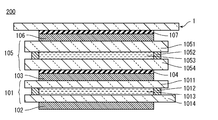
- FIG. 2 is a cross-sectional view showing a schematic configuration of a display device with a touch panel according to another embodiment of the present invention.
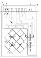
- FIG. 3 is a plan view showing a schematic configuration of the touch panel according to the first embodiment of the present invention.
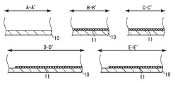
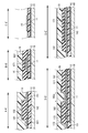
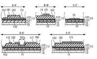
- 4 is a cross-sectional view taken along lines A-A ′, B-B ′, C-C ′, D-D ′, and E-E ′ in FIG. 3.
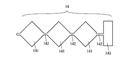
- FIG. 5 is a plan view showing one of the X electrodes extracted.
- FIG. 6 is a plan view showing one of the Y electrodes extracted.
- FIG. 5 is a plan view showing one of the X electrodes extracted.
- FIG. 7A is a cross-sectional view for explaining the method for manufacturing the touch panel according to the first embodiment of the present invention.
- FIG. 7B is a cross-sectional view for explaining the method for manufacturing the touch panel according to the first embodiment of the present invention.
- FIG. 7C is a cross-sectional view for explaining the touch panel manufacturing method according to the first embodiment of the present invention.
- FIG. 7D is a cross-sectional view for explaining the method for manufacturing the touch panel according to the first embodiment of the present invention.
- FIG. 7E is a cross-sectional view for explaining the touch panel manufacturing method according to the first embodiment of the present invention.
- FIG. 7F is a cross-sectional view for explaining the touch panel manufacturing method according to the first embodiment of the present invention.
- FIG. 7G is a cross-sectional view for explaining the method for manufacturing the touch panel according to the first embodiment of the present invention.
- FIG. 7H is a cross-sectional view for explaining the method for manufacturing the touch panel according to the first embodiment of the present invention.
- FIG. 8 is a plan view illustrating a schematic configuration of the touch panel according to the first comparative example.
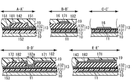
- FIG. 9 is a cross-sectional view taken along lines A-A ′, B-B ′, C-C ′, D-D ′, and E-E ′ in FIG. 8.
- FIG. 10 is a plan view showing a schematic configuration of a touch panel according to a second comparative example.
- FIG. 10 is a plan view showing a schematic configuration of a touch panel according to a second comparative example.
- FIG. 11 is a cross-sectional view taken along lines A-A ′, B-B ′, C-C ′, D-D ′, and E-E ′ in FIG. 10.
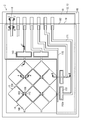
- FIG. 12 is a plan view showing a schematic configuration of a touch panel according to the second embodiment of the present invention.
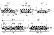
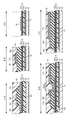
- FIG. 13 is a cross-sectional view taken along lines A-A ′, B-B ′, C-C ′, D-D ′, and E-E ′ in FIG. 12.
- FIG. 14A is sectional drawing for demonstrating the manufacturing method of the touchscreen concerning the 2nd Embodiment of this invention.
- FIG. 14B is a cross-sectional view for explaining the method for manufacturing the touch panel according to the second embodiment of the present invention.
- FIG. 14A is sectional drawing for demonstrating the manufacturing method of the touchscreen concerning the 2nd Embodiment of this invention.
- FIG. 14B is a cross-sectional view for explaining the method for manufacturing the touch panel according to the second embodiment of the present
- FIG. 14C is a cross-sectional view for explaining the method for manufacturing the touch panel according to the second embodiment of the present invention.
- FIG. 14D is a cross-sectional view for explaining the method for manufacturing the touch panel according to the second embodiment of the present invention.
- FIG. 14E is a cross-sectional view for explaining the method for manufacturing the touch panel according to the second embodiment of the present invention.
- a touch panel includes a translucent substrate, a light shielding film formed on a part of the substrate, a planarization film formed to cover the substrate and the light shielding film, and the flat surface.
- a barrier film formed to cover the conversion film, a sensor electrode formed on the barrier film, and a layer farther from the substrate than the planarization film, and is formed in a portion overlapping the light shielding film in plan view.
- a wiring that is formed in a layer farther from the substrate than the planarizing film and electrically connects the sensor electrode and the terminal.
- the barrier film is formed on the planarization film side and is formed of a first inorganic film made of an inorganic material and an inorganic material formed on the first inorganic film and having a refractive index lower than that of the first inorganic film.
- a second inorganic film (first configuration).
- the planarization film is formed so as to cover the substrate and the light shielding film.
- the step due to the light shielding film is flattened by the flattening film. For this reason, the layer farther from the substrate than the planarizing film is not affected by the step of the light shielding film. Accordingly, even if the sensor electrode or the wiring is formed so as to straddle the light shielding film in plan view, the sensor electrode or the wiring is not interrupted by the step of the light shielding film.
- the barrier film is further formed so as to cover the planarizing film, and the sensor electrode is formed on the barrier film.
- the barrier film includes an inorganic film and shields moisture and impurities from the planarization film. This can prevent the resistance of the sensor electrode from increasing due to the influence of moisture or impurities in the planarization film.
- the barrier film further includes a first inorganic film formed on the flattening film side and a second inorganic film having a refractive index lower than that of the first inorganic film.
- the inorganic film becomes denser as the refractive index is higher, and becomes coarser as the refractive index is lower. Therefore, the first inorganic film is a denser film than the second inorganic film and has a high barrier performance.
- the second inorganic film is a coarser film than the first inorganic film and has high reactivity.
- the refractive index of the first inorganic film may be 1.72 to 1.98, and the refractive index of the second inorganic film may be 1.41 to 1.68 (second Configuration).
- the thickness of the first inorganic film is preferably 3 to 12 nm, and the thickness of the second inorganic film is preferably 30 to 160 nm (third configuration).
- the transmittance of the sensor electrode can be increased by the interference action of the reflected light from the interface between the films. This makes it difficult for the user to visually recognize the sensor electrode.
- the first inorganic film may include a silicon nitride film (fourth configuration).
- the second inorganic film may contain either silicon oxide or silicon oxynitride (fifth configuration).
- the wiring is preferably formed in a portion overlapping the light shielding film in a plan view (sixth configuration).
- the wiring is not visually recognized by the user due to the light shielding film. Therefore, it is not necessary to form the wiring with a material having high transmittance. Therefore, for example, a metal film with low electrical resistance can be used as the wiring.
- the terminal is formed on the barrier film (seventh configuration).
- the resistance of the terminal can be prevented from being increased due to the influence of moisture of the planarizing film.
- This also eliminates the need for the terminal to be formed of a moisture resistant material or to be thick. Therefore, for example, it is possible to reduce the number of manufacturing steps by forming the sensor electrode and the terminal by the same material and the same process.
- a display device with a touch panel includes a liquid crystal display device and the touch panel having any one of the first to seventh configurations (first configuration of the display device with a touch panel).
- FIG. 1 is a cross-sectional view illustrating a schematic configuration of a display device 100 with a touch panel according to an embodiment of the present invention.
- a display device with a touch panel 100 includes a touch panel 1, a liquid crystal display device 101, polarizing plates 102 and 103, and a patch 104.
- Polarizing plates 102 and 103 are disposed on the front and back surfaces of the liquid crystal display device 101.
- the touch panel 1 is attached to the polarizing plate 103 by the adhesive material 104.
- the touch panel 1 has a sensor electrode on the surface on the liquid crystal display device 101 side, which will be described in detail later.
- the sensor electrode forms a capacitance between the sensor electrode and a finger close to the touch panel 1.
- the touch panel 1 detects the position of a finger or the like based on the change in capacitance.
- a light shielding film is formed in a predetermined area of the touch panel 1.
- the portion that the user does not want to visually recognize can be hidden by the light shielding film.
- the parts that the user does not want to see are, for example, the wiring and terminals of the touch panel 1 and the terminals of the liquid crystal display device 101.
- the liquid crystal display device 101 includes a color filter substrate 1011, a TFT (Thin Film Transistor) substrate 1014, a sealing material 1012, and a liquid crystal 1013.
- the color filter substrate 1011 and the TFT substrate 1014 are arranged to face each other.
- a sealing material 1012 is formed on the peripheral edge portions of the color filter substrate 1011 and the TFT substrate 1014, and a liquid crystal 1013 is sealed therein.
- the TFT substrate 1014 has a larger area than the color filter substrate 1011. In a region where the TFT substrate 1014 and the color filter substrate 1011 are pasted together, a terminal (not shown) is formed. This terminal is connected to a drive circuit (not shown) via, for example, an FPC (Flexible Printed Circuit).
- FPC Flexible Printed Circuit
- the TFT substrate 1014 includes pixel electrodes and TFTs (not shown).
- the pixel electrode and the TFT are formed in a matrix.
- As the TFT one containing amorphous silicon or IZGO (Indium Zinc Gallium Oxide) can be used, but one containing IZGO having a high electron mobility is preferably used.
- the color filter substrate 1011 includes a color filter (not shown) and a common electrode.
- the color filter is regularly formed so as to correspond to the pixel electrode of the TFT substrate 1014.
- the common electrode is uniformly formed in the active area of the TFT substrate 1014.
- the liquid crystal display device 101 drives the TFT of the TFT substrate 1014, generates an electric field between any pixel electrode and the common electrode, and controls the orientation of the liquid crystal 1013.
- the liquid crystal display device 101 controls transmission and non-transmission of light for each pixel by the orientation of the liquid crystal 1013 and the polarizing plates 102 and 103. As a result, an image is displayed on the liquid crystal display device 101.
- the substrate of the touch panel 1 also serves as a cover glass or a cover film. That is, it is not necessary to further bond a cover glass or a cover film on the touch panel 1. Thereby, a manufacturing process can be simplified. Moreover, the fall of the yield by mixing of the bubble and foreign material which occur when bonding the touch panel 1 and a cover glass or a cover film can be avoided. Furthermore, by omitting a member such as a cover glass, the liquid crystal display device 101 can be thinned and the light transmittance can be improved.
- FIG. 2 is a cross-sectional view showing a schematic configuration of a display device 200 with a touch panel according to another embodiment of the present invention.
- the display device with a touch panel 200 further includes a switch liquid crystal panel 105, a polarizing plate 106, and an adhesive material 107 in addition to the configuration of the display device with a touch panel 100.
- the switch liquid crystal panel 105 is attached to the polarizing plate 103 by the adhesive material 104.
- the polarizing plate 106 is disposed on the surface of the switch liquid crystal panel 105 opposite to the liquid crystal display device 101.
- the touch panel 1 is attached to the polarizing plate 106 with the adhesive material 107.
- the switch liquid crystal panel 105 includes a control substrate 1051, a counter substrate 1054, a sealing material 1052, and a liquid crystal 1053.
- the control substrate 1051 and the counter substrate 1054 are disposed to face each other.
- a sealing material 1052 is formed on the peripheral edge portions of the control substrate 1051 and the counter substrate 1054, and a liquid crystal 1053 is sealed inside.
- the control board 1051 includes a control electrode (not shown).
- the control electrodes are regularly arranged on the control board 1051.
- the counter substrate 1054 includes a common electrode (not shown).
- the common electrode is uniformly formed in the active area of the counter substrate 1054.
- the switch liquid crystal panel 105 generates an electric field between an arbitrary control electrode and a common electrode, and changes the alignment of the liquid crystal 1053.
- the display device 200 with a touch panel switches between the two-dimensional display mode and the three-dimensional display mode as follows.
- the liquid crystal 1053 of the switch liquid crystal panel 105 is uniformly oriented. Thereby, the image displayed on the liquid crystal display device 101 is displayed as it is.
- the switch liquid crystal panel 105 regularly changes the orientation of the liquid crystal 1053.
- the liquid crystal 1053 functions as a lens due to a difference in refractive index accompanying a change in orientation.
- the display device 200 with a touch panel causes the liquid crystal display device 101 to display images that are photographed from multiple directions in a line. The images that are regularly arranged and displayed are separated by the liquid crystal 1053.
- the display device 200 with a touch panel is observed at an optimal position, different images reach the left and right eyes. That is, the display device 200 with a touch panel performs three-dimensional display by a so-called parallax method in the three-dimensional display mode.
- the substrate of the touch panel 1 also serves as a cover glass or a cover film.
- FIG. 3 is a plan view schematically showing a schematic configuration of the touch panel 1 according to the first embodiment of the present invention.
- 4 is a cross-sectional view taken along lines AA ′, BB ′, CC ′, DD ′, and EE ′ in FIG.
- the touch panel 1 includes a substrate 10, a light shielding film 11, a planarizing film 12, a barrier film 13, an X electrode 14, a Y electrode 15, a terminal 16, a wiring 171, a ground wiring 172, insulating films 181 and 182, and a protective film 19. ing.
- the substrate 10 has translucency.
- the substrate 10 is, for example, a glass substrate or a transparent resin film.
- the substrate 10 may have a surface coated with a passivation film or the like.
- the light shielding film 11, the planarizing film 12, the barrier film 13, the X electrode 14, the Y electrode 15, the terminal 16, the wiring 171, the ground wiring 172, the insulating films 181 and 182, and the protective film 19 are formed on one surface of the substrate 10. Is formed. In the display device 100 with a touch panel, this surface is disposed on the liquid crystal display device 101 side.
- the touch panel 1 has a sensing area V and a non-sensing area P.
- the sensing area V is an area that is detected when a finger or the like touches the touch panel 1. That is, the region where the sensor electrodes (X electrode 14 and Y electrode 15) are formed is the sensing region V.
- the sensing area V is not limited to the rectangular area as shown in FIG. 3, and can take any shape. Further, it may be a discontinuous region.
- the sensing area V is preferably used so as to overlap with the display area of the liquid crystal display device 101. According to this configuration, the user can specify a position corresponding to the image displayed on the liquid crystal display device 101.
- the non-sensing area P is arranged on the right side and the lower part of the sensing area V.
- the arrangement of the non-sensing area P is arbitrary.
- the non-sensing region P may be arranged so as to surround the four sides of the sensing region V.
- the non-sensing area P may be arranged in contact with only one side of the sensing area V.
- the light shielding film 11 is formed on the substantially entire surface of the non-sensing region P.
- the light shielding film 11 may be formed only in a part of the non-sensing region P.
- the light shielding film 11 has a light shielding property.
- the light shielding film 11 is, for example, a black resin.
- the light shielding film 11 can prevent the components formed in a layer farther from the substrate 10 than the light shielding film 11 from being visually recognized by the user.
- a planarizing film 12 is formed so as to cover the substrate 10 and the light shielding film 11.
- the planarizing film 12 is formed so as to eliminate a step between the substrate 10 and the light shielding film 11.
- the planarizing film 12 can be formed of a light transmitting resin, for example.
- a barrier film 13 is formed so as to cover the planarizing film 12.
- the barrier film 13 is formed so as to cover substantially the entire surface of the planarizing film 12.
- the barrier film 13 preferably covers substantially the entire surface of the planarization film 12.
- the barrier film 13 may be formed only on a part of the planarizing film 12.
- the barrier film 13 includes a first inorganic film 131 formed on the planarizing film 12 side and a second inorganic film 132 formed on the first inorganic film 131.
- the second inorganic film 132 is formed of a material having a refractive index lower than that of the first inorganic film 131.
- the X electrode 14, the Y electrode 15, the terminal 16, the wiring 171, the ground wiring 171, the insulating films 181 and 182, and the protective film 19 are formed on the barrier film 13.
- FIG. 5 is a plan view showing one of the X electrodes 14 extracted.
- the X electrode 14 includes a plurality of island-shaped electrodes 141 arranged along one direction, and a connection portion 142 that connects adjacent island-shaped electrodes 141.
- the X electrode 14 further includes a connection portion 143 for connecting to the wiring 171 at one end in the extending direction.
- the island-shaped electrode 141 and the connecting portions 142 and 143 are integrally formed.
- FIG. 6 is a plan view showing one of the Y electrodes 15 extracted.
- the Y electrode 15 includes a plurality of island-shaped electrodes 151 arranged along a direction intersecting the X electrode 14 and a connection portion 152 that connects the adjacent island-shaped electrodes 151.
- the Y electrode 15 further includes a connection portion 153 for connecting to the wiring 171 at one end in the extending direction.
- the island-shaped electrode 151 and the connection parts 152 and 153 are formed in different steps as will be described later.
- the X electrode 14 and the Y electrode 15 are formed of a material having translucency and conductivity.
- the X electrode 14 and the Y electrode 15 are, for example, ITO (Indium Tin Oxide) or IZO (Inzium Zinc Oxide).
- An insulating film 181 is formed at a location where the X electrode 14 and the Y electrode 15 intersect.
- the connecting portion 152 of the Y electrode 15 connects adjacent island electrodes 151 via the insulating film 181. With this configuration, the X electrode 14 and the Y electrode 15 are insulated from each other.
- the terminal 16 is formed in the non-sensing area P.
- the terminal 16 is connected to a drive circuit (not shown) via, for example, an FPC. Therefore, the terminal 16 is exposed from the insulating film 182 and the protective film 19. Therefore, the terminal 16 is preferably formed of a material having high corrosion resistance.
- the terminal 16 is, for example, ITO or IZO.
- the wiring 171 electrically connects the X electrode 14 and the terminal 16, and the Y electrode 15 and the terminal 16. More specifically, the wiring 171 that connects the X electrode 14 and the terminal 16 is in contact with the terminal 16 and the connection portion 143 of the X electrode 14. The wiring 171 that connects the Y electrode 15 and the terminal 16 is in contact with the terminal 16 and the connection portion 153 of the Y electrode 15. Note that the wiring 171 and the connection portion 153 are in contact with each other through a contact hole 182 a formed in the insulating film 182.
- the ground wiring 172 is connected only to the terminal 16 and is not connected to the X electrode 14 and the Y electrode 15.
- the ground wiring 172 functions as a shield line that shields electromagnetic noise.
- the wiring 171 and the ground wiring 172 are, for example, metal films.
- An insulating film 182 is formed to cover the wiring 171 and the ground wiring 172.
- the insulating film 182 protects the wiring 171 and the ground wiring 172 from chemicals used in a later process when the touch panel 1 is manufactured.
- the insulating film 182 protects the wiring 171 and the ground wiring 172 from moisture in the environment.
- the insulating film 182 also functions as an interlayer insulating film that prevents the connection portion 15 of the Y electrode 15 and the ground wiring 172 from being short-circuited.
- the protective film 19 is formed so as to cover substantially the entire surface of the substrate 10. As described above, a part of the substrate 10 and the terminal 16 is exposed without being covered with the protective film 19.
- the insulating films 181 and 182 and the protective film 19 are made of a light-transmitting insulating material.
- the insulating films 181 and 182 and the protective film 19 may each be an organic material or an inorganic material.
- FIGS. 7A to 7H are sectional views taken along lines AA ′, BB ′, CC ′, DD ′, and EE ′ in FIG. is there.
- a light shielding film 11 is formed on the substrate 10.
- a low reflection metal such as chromium or a black resin can be used, but it is preferable to use a black resin.
- the black resin is obtained, for example, by dispersing a black pigment in an acrylic resin or a novolac resin.
- Examples of the method for forming the light shielding film 11 include a printing method such as a screen printing method and a flexo printing method, or patterning by photolithography.
- planarizing film 12 is formed so as to cover the light shielding film 11.
- the planarizing film 12 can be mainly composed of, for example, acrylic resin, novolac resin, epoxy resin, alkyl resin, phenol resin, or silicon resin.
- the planarizing film 12 is formed in a predetermined region of the substrate 10 by, for example, a spin coater or a slit coater.
- the thickness of the planarizing film 12 is not particularly limited as long as it is thicker than the light shielding film 11, but is, for example, 1.5 to 3.5 ⁇ m.
- a barrier film 13 is formed so as to cover the planarizing film 12.
- the barrier film 13 has a laminated structure of the first inorganic film 131 and the second inorganic film 132 as described above.
- the second inorganic film 132 is made of a material having a refractive index lower than that of the first inorganic film 131.
- the refractive index of the first inorganic film 131 is preferably 1.72 to 1.98.
- the refractive index of the second inorganic film 132 is preferably 1.41 to 1.68.
- the first inorganic film is, for example, silicon nitride (SiN).
- the second inorganic film is, for example, silicon oxide (SiO) or silicon oxynitride (SiON).
- the first inorganic film 131 and the second inorganic film 132 are formed by, for example, CVD (Chemical Vapor Deposition).
- the refractive indexes of the first inorganic film 131 and the second inorganic film 132 can be adjusted by, for example, the gas flow rate, pressure, and heating temperature during film formation.
- the thickness of the first inorganic film 131 is preferably 3 to 12 nm
- the thickness of the second inorganic film 132 is preferably 30 to 160 nm.
- connecting portions 142 and 143 of the X electrode 14, island-shaped electrodes 151 of the Y electrode 15, and terminals 16 are formed.
- the island electrode 141 of the X electrode 14 is also formed in this step.
- a uniform transparent conductive film is formed by sputtering or CVD.
- the transparent conductive film is, for example, ITO or IZO.
- the thickness of the transparent conductive film is, for example, 10 to 50 nm.
- the formed transparent conductive film is patterned by photolithography. Specifically, a mask made of a photoresist is formed at the locations where the island-shaped electrodes 141 and 151, the connection portions 142 and 143, and the terminal 16 are to be formed.
- Etching can be performed using, for example, a mixed acid of phosphoric acid, acetic acid, and nitric acid, or oxalic acid.
- annealing is performed in a temperature range of 200 to 250 ° C. By this annealing, the amorphous transparent conductive film is polycrystallized.
- the X electrode 14, a part of the Y electrode 15, and the terminal 16 are formed by the same material and the same process.
- a wiring 171 and a ground wiring 172 are formed.
- a uniform metal film is formed by, for example, sputtering or vapor deposition.
- the metal film preferably has a low resistance, and for example, Al is used.
- a conductive oxide film such as ITO
- galvanic corrosion may occur due to a difference in ionization tendency. Therefore, a laminated structure with a metal having high corrosion resistance is preferable. Therefore, for example, a laminated film of MoNb, Al, and MoNb, a laminated film of MoN, Al, and MoN, or a laminated film of Mo, Al, and Mo is preferably used as the metal film.
- the thickness of the metal film is, for example, 0.3 to 1.0 ⁇ m.
- the formed metal film is patterned by photolithography. Specifically, a mask made of a photoresist is formed at a place where the wiring 171 and the ground wiring 172 are formed. Then, the remaining part is removed by etching. Etching can be performed using, for example, a mixed acid of phosphoric acid, acetic acid, and nitric acid.
- insulating films 181 and 182 are formed.
- the insulating films 181 and 182 either an organic material or an inorganic material may be used.
- the organic material is, for example, a photoresist containing an acrylic resin or a novolac resin.
- Photoresist is uniformly applied to the substantially entire surface of the substrate 10 by a spin coater or a slit coater.
- the thickness of the photoresist is not particularly limited, but is, for example, 1.5 to 3.0 ⁇ m.
- the formed photoresist is patterned by photolithography to form insulating films 181 and 182. At this time, a contact hole 182a is also formed.
- the inorganic material is, for example, SiN, SiO, or SiON.
- a uniform film of these substances is formed on the substantially entire surface of the substrate 10 by CVD.
- the thickness of the film is preferably thicker, and is preferably twice or more the thickness of the wiring 171 and the ground wiring 172.
- the formed film is patterned by photolithography. Specifically, a mask made of a photoresist is formed at a place where the insulating films 181 and 182 are formed. Then, the remaining part is removed by etching. At this time, a contact hole 182a is also formed.
- etching for example, dry etching using a fluorine-based gas can be used.
- the insulating films 181 and 182 preferably have a forward tapered shape in cross section. That is, it is preferable that the cross sections of the insulating films 181 and 182 have a tapered shape that is convex toward the side opposite to the substrate 10. This is because the connection portions 152 and 153 (see FIG. 7G) formed on the insulating films 181 and 182 can be prevented from being interrupted by a step at the boundary between the insulating films 181 and 182.
- a forward tapered shape can be formed by performing exposure using a photomask whose light transmittance changes stepwise.
- a forward tapered shape can be formed by adjusting etching conditions or stacking films.
- connecting portions 152 and 153 of the Y electrode 15 are formed.
- a uniform transparent conductive film is formed by sputtering or CVD.
- the transparent conductive film is, for example, ITO or IZO.
- the thickness of the transparent conductive film is, for example, 10 to 50 nm.
- the formed transparent conductive film is patterned by photolithography. Specifically, a mask made of a photoresist is formed at a location where the connection portions 152 and 153 are to be formed. Then, the remaining part is removed by etching. For the etching, for example, a mixed acid of phosphoric acid, acetic acid and nitric acid, or oxalic acid can be used. After the patterning is finished, annealing for polycrystallizing the connection portions 152 and 153 may be performed.
- a protective film 19 is formed so as to cover almost the entire surface of the substrate 10.
- the protective film 19 may use either an organic material or an inorganic material.
- the organic material is, for example, an acrylic resin, and is formed by a spin coater or a slit coater.
- the inorganic material is SiN, for example, and is formed by CVD. In either case, the protective film 19 is formed using a mask or the like so that a part of the terminal 16 is exposed.
- the planarization film 12 is formed so as to cover the substrate 10 and the light shielding film 11. A level difference due to the light shielding film 11 is flattened by the flattening film 12. For this reason, the layer farther from the substrate 10 than the planarizing film 12 is not affected by the step of the light shielding film 11.
- the connection part 143 of the X electrode 14 and the connection part 153 of the Y electrode 15 are formed across the light shielding film 11 in plan view. However, the connecting portions 143 and 153 are not interrupted by the planarizing film 12.
- the surface roughness of the light shielding film 11 depends on the particle diameter of the pigment. When the surface roughness of the light shielding film 11 is large, it becomes difficult to form a uniform thin film on the light shielding film 11. By forming the planarizing film 12 so as to cover the light shielding film 11, the surface can be smoothed.
- a barrier film 13 is formed so as to cover the planarizing film 12.
- the planarizing film 12 may contain a residual solvent. Further, the planarizing film 12 may be exposed to and absorbed by a photolithography developer and a cleaning solution during the manufacturing process. Further, the planarizing film 12 may absorb moisture in the atmosphere. These moisture or impurities may spring out on the surface of the planarization film 12 during the manufacturing process.
- a transparent conductive film is formed on the surface from which moisture or impurities are swelled, the resistance of the transparent conductive film may increase due to the influence of moisture or impurities.
- a transparent conductive film is formed on the barrier film 13. Thereby, it is possible to prevent the resistance of the transparent conductive film from increasing.
- the barrier film 13 has a laminated structure of the first inorganic film 131 and the second inorganic film 132.
- the refractive index of the second inorganic film 132 is lower than the refractive index of the first inorganic film 131.
- the inorganic film becomes denser as the refractive index is higher, and becomes coarser as the refractive index is lower. Therefore, the first inorganic film 131 is a denser film than the second inorganic film 132 and has a high barrier performance.
- the second inorganic film 132 is a coarser film than the first inorganic film 131 and has high reactivity.
- the thickness of the first inorganic film 131 is preferably 3 to 12 nm, and the thickness of the second inorganic film 132 is preferably 30 to 160 nm.
- the X electrode 14 and the Y electrode 15 are used so as to overlap the display area of the liquid crystal display device 101 (see FIG. 1). Therefore, it is preferable that the X electrode 14 and the Y electrode 15 are not easily seen by the user, that is, the light transmittance is high. According to this embodiment, the light transmittance of the X electrode 14 and the Y electrode 15 can be increased by the interference action of the reflected light from the interface between the films.
- the above numerical range was obtained as follows.
- the thickness of the first inorganic film 131 was fixed to 9 nm, and the thickness of the second inorganic film 132 was changed.
- the thickness of the second inorganic film 132 was less than 30 nm, the X electrode 14 and the Y electrode 15 were easily visually recognized.
- the thickness of the second inorganic film 132 is thicker than 160 nm, the X electrode 14 and the Y electrode 15 are easily visually recognized.
- the thickness of the second inorganic film 132 was fixed to 90 nm, and the thickness of the first inorganic film 131 was changed.
- the thickness of the first inorganic film 131 was thinner than 3 nm, the X electrode 14 and the Y electrode 15 were easily visually recognized.
- the film thickness of the 1st inorganic film 131 was thicker than 12 nm, the X electrode 14 and the Y electrode 15 became easy to visually recognize. From the above, it is preferable that the thickness of the first inorganic film 131 is 3 to 12 nm and the thickness of the second inorganic film 132 is 30 to 160 nm.
- the wiring 171 and the ground wiring 172 are formed only in the non-sensing region P. Accordingly, the wiring 171 and the ground wiring 172 overlap the light shielding film 11 in plan view. Therefore, the wiring 171 and the ground wiring 172 are not visually recognized by the user. Therefore, a material with high reflectivity can be used for the wiring 171 and the ground wiring 172.
- the barrier film 13 is formed so as to cover substantially the entire surface of the planarizing film 12.
- the terminal 16 is also formed on the barrier film 13. Therefore, even when the planarizing film 12 contains water or impurities, the terminal 16 can be prevented from increasing in resistance.
- the X electrode 14, a part of the Y electrode 15, and the terminal 16 are formed by the same material and the same process. As a result, the number of manufacturing steps can be reduced.
- the X electrode 14 and the Y electrode 15 are preferably formed thin in order to increase the light transmittance. Since the barrier film 13 can prevent the resistance of the terminal 16 from being increased, the terminal 16 can function even if it is a thin film.
- FIG. 8 is a plan view showing a schematic configuration of the touch panel 8 according to the first comparative example.
- FIG. 9 is a cross-sectional view taken along lines AA ′, BB ′, CC ′, DD ′, and EE ′ in FIG.
- the touch panel 8 is obtained by removing the planarization film 12 and the barrier film 13 from the configuration of the touch panel 1.
- connection portion 143 of the X electrode 14 is formed across the light shielding film 11 in plan view.
- the light shielding film 11 is formed, for example, by mixing a negative resist with a pigment. Therefore, the amount of exposure at the pattern end tends to be insufficient, and it is difficult to form a forward tapered shape. For this reason, the connection portion 143 may be interrupted by the step of the light-shielding film 11 as shown in FIG.
- FIG. 10 is a plan view showing a schematic configuration of the touch panel 9 according to the second comparative example.
- FIG. 11 is a cross-sectional view taken along lines A-A ′, B-B ′, C-C ′, D-D ′, and E-E ′ in FIG. 9.
- the touch panel 9 is obtained by adding a planarizing film 12 to the configuration of the touch panel 8. In other words, the touch panel 9 is obtained by deleting the barrier film 13 from the configuration of the touch panel 1.
- connection portion 143 can be prevented from being interrupted by the planarization film 12.
- the planarizing film 12 contains water or impurities, the portion of the X electrode 14, Y electrode 15, and terminal 16 that is in contact with the planarizing film 12 is increased in resistance. As a result, the reliability may decrease or the sensor sensitivity may decrease.
- the touch panel 1 includes a planarizing film 12 and a barrier film 13.
- the planarization film 12 can prevent the connection portion 143 from being interrupted. Further, by forming the barrier film 13 on the planarizing film 12, even when the planarizing film 12 contains water or impurities, the X electrode 14, the Y electrode 15, and the terminal 16 do not increase in resistance. .
- the display device with a touch panel 100 may include a touch panel 2 described below instead of the touch panel 1.
- FIG. 12 is a plan view schematically showing a schematic configuration of the touch panel 2 according to the second embodiment of the present invention.
- 13 is a cross-sectional view taken along lines AA ′, BB ′, CC ′, DD ′, and EE ′ in FIG.
- the touch panel 2 is different from the touch panel 1 in the formation order of the constituent elements. Thereby, the stacking order of each film is different.
- FIGS. 14A to 14E are sectional views taken along lines AA ′, BB ′, CC ′, DD ′, and EE ′ in FIG. is there.
- a light shielding film 11, a flat film 12, and a barrier film 13 are formed on the substrate 10. Since the steps up to here are the same as those of the touch panel 1, the illustration thereof is omitted.
- connecting portions 152 and 153 of the Y electrode 15 are formed.
- insulating films 181 and 183 are formed.
- the connecting portions 142 and 143 of the X electrode 14, the island-shaped electrode 151 of the Y electrode 15, and the terminal 16 are formed.
- the island electrode 141 of the X electrode 14 is also formed in this step.
- a wiring 171 and a ground wiring 172 are formed.
- a protective film 19 is formed.
- connection part 143 of the X electrode 14 and the connection part 153 of the Y electrode 15 are formed across the light shielding film 11 in a plan view. Also in this case, the planarization film 12 can prevent the connection parts 143 and 153 from being interrupted by the step of the light shielding film 11.
- the barrier film 13 is formed on the flattening film 12, so that the X electrode 14, the Y electrode 15, and the terminal 16 are formed even when the flattening film 12 contains water or impurities. There is no increase in resistance.
- the present invention can be industrially used as a touch panel and a display device with a touch panel.
Landscapes
- Engineering & Computer Science (AREA)
- Physics & Mathematics (AREA)
- General Engineering & Computer Science (AREA)
- Theoretical Computer Science (AREA)
- General Physics & Mathematics (AREA)
- Human Computer Interaction (AREA)
- Nonlinear Science (AREA)
- Mathematical Physics (AREA)
- Chemical & Material Sciences (AREA)
- Crystallography & Structural Chemistry (AREA)
- Optics & Photonics (AREA)
- Position Input By Displaying (AREA)
Abstract
カバー一体型のタッチパネルの構成において、センサ電極と配線とを確実に接続できる、信頼性の高い構成を得る。タッチパネル(1)は、透光性の基板(10)と、前記基板(10)の一部に形成された遮光膜(11)と、前記基板(10)および前記遮光膜(11)を覆って形成された平坦化膜(12)と、前記平坦化膜(12)を覆って形成されたバリア膜(13)と、前記バリア膜(13)に形成されたセンサ電極(14),(15)と、平面視において前記遮光膜(11)に重なる部分に形成された端子(16)と、前記センサ電極(14),(15)と前記端子(16)とを電気的に接続する配線(171)とを備える。前記バリア膜(13)は、前記平坦化膜(12)側に形成され、無機物によって構成された第1無機膜(131)と、前記第1無機膜(131)に形成され、前記第1無機膜よりも屈折率の低い無機物によって構成された第2無機膜(132)とを含む。
Description
本発明は、タッチパネルおよびタッチパネル付き表示装置に関し、より詳しくは、カバーガラス一体型のタッチパネルおよびタッチパネル付き表示装置に関する。
タッチパネルは、カバーガラスまたはカバーフィルムと貼り合せて使用される。タッチパネルとカバーガラスとを貼り合せる際、気泡や異物が混入することがあり、歩留まり低下の原因となっている。
従来、カバーガラスの裏面(操作面と反対側の面)にセンサ電極を形成してタッチパネルとした、カバーガラス一体型のタッチパネルの構成が知られている。すなわち、この構成では、タッチパネルの基板がカバーガラス(カバーフィルム)の役割を兼ねる。
特開2011-90443号公報には、1枚の透明基板の片側の面に、第1の方向に延びる電極と、前記第1の方向と交差する方向である第2の方向に延びる電極とが形成され、前記透明基板の周辺部に、遮光性を有する材料によるブラックマスク部(遮光膜)が設けられていることを特徴とする投影型静電容量タッチパネルが記載されている。
ブラックマスク部は、例えば、透明基板の周辺部に形成される電極の引き廻し配線および信号処理用の接続部を視認側に対して覆い隠すように設けられている。ブラックマスク部として、顔料タイプのカラーフィルタ材料を用いることが開示されている。
上記のように、タッチパネルの非センシング領域に遮光膜を設け、配線等を、遮光膜に重ねて形成することでユーザに視認されないようにする構成が知られている。しかしながら、センサ電極や配線等の導電膜を、遮光膜の形成された領域と形成されていない領域とにまたがって形成しようとすると、遮光膜の段差によって、導電膜が途切れてしまう場合がある。
本発明の目的は、カバー一体型のタッチパネルの構成において、センサ電極と配線とを確実に接続できる、信頼性の高い構成を得ることである。
ここに開示するタッチパネルは、透光性の基板と、前記基板の一部に形成された遮光膜と、前記基板および前記遮光膜を覆って形成された平坦化膜と、前記平坦化膜に形成されたバリア膜と、前記バリア膜に形成されたセンサ電極と、前記平坦化膜よりも前記基板から遠い層であって、平面視において前記遮光膜に重なる部分に形成された端子と、前記平坦化膜よりも前記基板から遠い層に形成され、前記センサ電極と前記端子とを電気的に接続する配線とを備える。前記バリア膜は、前記平坦化膜側に形成され、無機物によって構成された第1無機膜と、前記第1無機膜に形成され、前記第1無機膜よりも屈折率の低い無機物によって構成された第2無機膜とを含む。
本発明によれば、カバー一体型のタッチパネルの構成において、センサ電極と配線とを確実に接続できる、信頼性の高い配線の構成が得られる。
本発明の一実施形態にかかるタッチパネルは、透光性の基板と、前記基板の一部に形成された遮光膜と、前記基板および前記遮光膜を覆って形成された平坦化膜と、前記平坦化膜を覆って形成されたバリア膜と、前記バリア膜に形成されたセンサ電極と、前記平坦化膜よりも前記基板から遠い層であって、平面視において前記遮光膜に重なる部分に形成された端子と、前記平坦化膜よりも前記基板から遠い層に形成され、前記センサ電極と前記端子とを電気的に接続する配線とを備える。前記バリア膜は、前記平坦化膜側に形成され、無機物によって構成された第1無機膜と、前記第1無機膜に形成され、前記第1無機膜よりも屈折率の低い無機物によって構成された第2無機膜とを含む(第1の構成)。
上記の構成によれば、基板および遮光膜を覆って、平坦化膜が形成される。平坦化膜によって、遮光膜による段差が平坦化される。このため、平坦化膜よりも基板から遠い層では、遮光膜の段差の影響を受けない。これによって、平面視において遮光膜をまたがるようにセンサ電極または配線を形成しても、センサ電極または配線は遮光膜の段差によって途切れることがない。
上記の構成によればさらに、平坦化膜を覆ってバリア膜が形成され、バリア膜にセンサ電極が形成される。バリア膜は無機物の膜を含み、平坦化膜からの水分および不純物を遮蔽する。これによって、平坦化膜の水分または不純物の影響を受けて、センサ電極が高抵抗化することを防止できる。
上記の構成によればさらに、バリア膜は、平坦化膜側に形成される第1無機膜と、第1無機膜よりも屈折率の低い第2無機膜とを含む。無機物の膜は、一般的に、屈折率が高いほど緻密な膜となり、屈折率が低いほど粗な膜となる。したがって、第1無機膜は第2無機膜よりも緻密な膜であり、バリア性能が高い。一方、第2無機膜は第1無機膜よりも粗な膜であり、反応性が高い。バリア膜を、第1無機膜および第2無機膜を含んだ積層構造にすることにより、高いバリア性能を得ながら、センサ電極との密着性を良くすることができる。
上記第1の構成において、前記第1無機膜の屈折率は1.72~1.98であり、前記第2無機膜の屈折率は1.41~1.68であっても良い(第2の構成)。
上記第2の構成において、前記第1無機膜の厚さは3~12nmであり、前記第2無機膜の厚さは30~160nmであることが好ましい(第3の構成)。
上記の構成によれば、各膜同士の界面からの反射光の干渉作用によって、センサ電極の透過率を高めることができる。これによって、センサ電極をユーザから視認されにくくすることができる。
上記第1~第3のいずれかの構成において、前記第1無機膜は窒化ケイ素膜を含んでいても良い(第4の構成)。
上記第1~第4のいずれかの構成において、前記第2無機膜は酸化ケイ素および酸窒化ケイ素のいずれかを含んでいても良い(第5の構成)。
上記第1~第5のいずれかの構成において、前記配線は、平面視において前記遮光膜に重なる部分に形成されることが好ましい(第6の構成)。
上記の構成によれば、配線は、遮光膜によってユーザに視認されない。したがって、透過率の高い材料で配線を形成しなくても良い。そのため、配線として例えば、電気抵抗の低い金属膜を用いることができる。
上記第1~第6のいずれかの構成において、前記端子は前記バリア膜に形成される、ことが好ましい(第7の構成)。
上記の構成によれば、平坦化膜の水分の影響を受けて、端子が高抵抗化することを防止できる。また、これによって、端子を耐湿性の材料で形成したり、端子を厚く形成したりする必要がなくなる。そのため、例えばセンサ電極と端子とを同一材料および同一工程で形成し、製造工程数を減らすことも可能になる。
本発明の一実施形態にかかるタッチパネル付き表示装置は、液晶表示装置と、上記第1~第7のいずれかの構成のタッチパネルとを備える(タッチパネル付き表示装置の第1の構成)。
[実施の形態]
以下、図面を参照し、本発明の実施の形態を詳しく説明する。図中同一または相当部分には同一符号を付してその説明は繰り返さない。なお、説明を分かりやすくするために、以下で参照する図面においては、構成が簡略化または模式化して示されたり、一部の構成部材が省略されたりしている。また、各図に示された構成部材間の寸法比は、必ずしも実際の寸法比を示すものではない。
以下、図面を参照し、本発明の実施の形態を詳しく説明する。図中同一または相当部分には同一符号を付してその説明は繰り返さない。なお、説明を分かりやすくするために、以下で参照する図面においては、構成が簡略化または模式化して示されたり、一部の構成部材が省略されたりしている。また、各図に示された構成部材間の寸法比は、必ずしも実際の寸法比を示すものではない。
[全体の構成]
図1は、本発明の一実施形態にかかるタッチパネル付き表示装置100の概略構成を示す断面図である。タッチパネル付き表示装置100は、タッチパネル1、液晶表示装置101、偏光板102および103、ならびに貼付材104を備えている。
図1は、本発明の一実施形態にかかるタッチパネル付き表示装置100の概略構成を示す断面図である。タッチパネル付き表示装置100は、タッチパネル1、液晶表示装置101、偏光板102および103、ならびに貼付材104を備えている。
液晶表示装置101の表裏の面に、偏光板102および103が配置されている。タッチパネル1は、貼付材104によって、偏光板103に貼り付けられている。
タッチパネル1は、詳しい構成は後述するが、液晶表示装置101側の面にセンサ電極を有している。センサ電極は、タッチパネル1に近接した指等との間に静電容量を形成する。タッチパネル1は、この静電容量の変化に基づいて、指等の位置を検出する。
また、タッチパネル1の所定の領域に、遮光膜が形成されている。遮光膜によって、ユーザに視認させたくない部分を隠すことができる。ユーザに視認させたくない部分とは、例えば、タッチパネル1の配線や端子、液晶表示装置101の端子等である。
液晶表示装置101は、カラーフィルタ基板1011、TFT(Thin Film Transistor)基板1014、シール材1012、および液晶1013を備えている。カラーフィルタ基板1011とTFT基板1014とは、互いに対向して配置されている。カラーフィルタ基板1011およびTFT基板1014の周縁部にはシール材1012が形成され、内部に液晶1013が封入されている。
TFT基板1014は、カラーフィルタ基板1011よりも大きな面積を有している。TFT基板1014とカラーフィルタ基板1011とを貼り合せてはみ出した領域には、図示しない端子が形成されている。この端子は、例えばFPC(Flexible Printed Circuit)を介して、図示しない駆動回路に接続される。
TFT基板1014は、図示しない画素電極とTFTとを備えている。画素電極とTFTとは、マトリクス状に形成されている。TFTとして、アモルファスシリコンやIZGO(Indium Zinc Gallium Oxide)を含むものを用いることができるが、電子移動度の大きいIZGOを含むものを用いることが好ましい。
カラーフィルタ基板1011は、図示しないカラーフィルタと共通電極とを備えている。カラーフィルタは、TFT基板1014の画素電極と対応するように規則的に形成されている。共通電極は、TFT基板1014のアクティブエリアに一様に形成されている。
液晶表示装置101は、TFT基板1014のTFTを駆動して、任意の画素電極と共通電極との間に電界を生成し、液晶1013の配向を制御する。液晶表示装置101は、液晶1013の配向と、偏光板102および103とによって、画素ごとに光の透過と非透過とを制御する。これによって、液晶表示装置101に画像が表示される。
以上、タッチパネル付き表示装置100の概略構成を説明した。タッチパネル付き表示装置100においては、タッチパネル1の基板が、カバーガラスまたはカバーフィルムの役割を兼ねている。すなわち、タッチパネル1の上にさらにカバーガラスまたはカバーフィルムを貼り合わせる必要がない。これにより、製造工程を簡略化できる。また、タッチパネル1とカバーガラスまたはカバーフィルムとを貼り合せる際に起こる気泡や異物の混入による、歩留まりの低下を避けることができる。さらに、カバーガラス等の部材を省くことにより、液晶表示装置101を薄型化でき、光透過度を向上させることができる。
図2は、本発明の他の実施形態にかかるタッチパネル付き表示装置200の概略構成を示す断面図である。タッチパネル付き表示装置200は、タッチパネル付き表示装置100の構成に加えてさらに、スイッチ液晶パネル105、偏光板106、および貼付材107を備えている。
スイッチ液晶パネル105は、貼付材104によって偏光板103に貼り付けられている。偏光板106は、スイッチ液晶パネル105の、液晶表示装置101と反対側の面に配置されている。タッチパネル1は、貼付材107によって偏光板106に貼り付けられている。
スイッチ液晶パネル105は、制御基板1051、対向基板1054、シール材1052、および液晶1053を備えている。制御基板1051と対向基板1054とは、互いに対向して配置されている。制御基板1051および対向基板1054の周縁部にはシール材1052が形成され、内部に液晶1053が封入されている。
制御基板1051は、図示しない制御電極を備えている。制御電極は、制御基板1051に規則的に配置されている。対向基板1054は、図示しない共通電極を備えている。共通電極は、対向基板1054のアクティブエリアに一様に形成されている。スイッチ液晶パネル105は、任意の制御電極と共通電極との間に電界を生成し、液晶1053の配向を変化させる。
タッチパネル付き表示装置200は、以下のようにして、2次元表示モードと、3次元表示モードとを切り替える。
2次元表示モードでは、スイッチ液晶パネル105の液晶1053は一様に配向している。これにより、液晶表示装置101に表示された画像が、そのまま表示される。
3次元表示モードでは、スイッチ液晶パネル105は、液晶1053の配向を規則的に変化させる。配向の変化に伴う屈折率差により、液晶1053はレンズとして機能する。これに対応して、タッチパネル付き表示装置200は、液晶表示装置101に、多方向から撮影した画像を規則的に並べて表示させる。規則的に並べて表示された画像は、液晶1053によって分離される。最適な位置でタッチパネル付き表示装置200を観察すると、左右の眼に異なる画像が届く。すなわち、タッチパネル付き表示装置200は、3次元表示モードでは、いわゆる視差方式による3次元表示を行う。
以上、タッチパネル付き表示装置200の概略構成を説明した。タッチパネル付き表示装置200においても、タッチパネル1の基板が、カバーガラスまたはカバーフィルムの役割を兼ねている。
[タッチパネルの構成]
[第1の実施形態]
以下、タッチパネル1の構成について詳しく述べる。図3は、本発明の第1の実施形態にかかるタッチパネル1の概略構成を模式的に示す平面図である。図4は、図3におけるA-A’線、B-B’線、C-C’線、D-D’線およびE-E’線の各線に沿った断面図である。タッチパネル1は、基板10、遮光膜11、平坦化膜12、バリア膜13、X電極14、Y電極15、端子16、配線171、グランド配線172、絶縁膜181および182、ならびに保護膜19を備えている。
[第1の実施形態]
以下、タッチパネル1の構成について詳しく述べる。図3は、本発明の第1の実施形態にかかるタッチパネル1の概略構成を模式的に示す平面図である。図4は、図3におけるA-A’線、B-B’線、C-C’線、D-D’線およびE-E’線の各線に沿った断面図である。タッチパネル1は、基板10、遮光膜11、平坦化膜12、バリア膜13、X電極14、Y電極15、端子16、配線171、グランド配線172、絶縁膜181および182、ならびに保護膜19を備えている。
基板10は透光性を有している。基板10は、例えばガラス基板または透明樹脂フィルムである。基板10は、表面がパシベーション膜等でコーティングされたものであっても良い。遮光膜11、平坦化膜12、バリア膜13、X電極14、Y電極15、端子16、配線171、グランド配線172、絶縁膜181および182、ならびに保護膜19は、基板10の一方の面に形成されている。タッチパネル付き表示装置100において、この面が液晶表示装置101側になるように配置される。
タッチパネル1は、センシング領域Vと、非センシング領域Pとを有している。センシング領域Vは、指等がタッチパネル1に接触した際に、検知される領域である。すなわち、センサ電極(X電極14およびY電極15)が形成されている領域が、センシング領域Vである。センシング領域Vは、図3のような矩形領域に限らず、任意の形状を取り得る。また、非連続領域であっても良い。センシング領域Vは、好ましくは液晶表示装置101の表示領域と重ね合わせて使用される。この構成によれば、ユーザは、液晶表示装置101に表示された画像と対応する位置を指示することができる。
図3では、非センシング領域Pを、センシング領域Vの右側部と下部とに配置している。しかし、非センシング領域Pの配置の仕方は任意である。例えば、非センシング領域Pを、センシング領域Vの四辺を囲むように配置しても良い。あるいは、非センシング領域Pを、センシング領域Vの一辺にのみ接して配置しても良い。
非センシング領域Pの概略全面に、遮光膜11が形成されている。遮光膜11は、非センシング領域Pの一部だけに形成されていても良い。遮光膜11は遮光性を有している。遮光膜11は、例えば黒色樹脂である。遮光膜11によって、遮光膜11よりも基板10から遠い層に形成された構成要素を、ユーザから視認されないようにすることができる。
基板10および遮光膜11を覆って、平坦化膜12が形成されている。平坦化膜12は、基板10と遮光膜11との段差をなくすように形成されている。平坦化膜12は、例えば透光性の樹脂によって形成することができる。
平坦化膜12を覆って、バリア膜13が形成されている。本実施形態では、バリア膜13は平坦化膜12の概略全面を覆って形成されている。本実施形態のように、バリア膜13は、平坦化膜12の概略全面を覆っていることが好ましい。しかし、バリア膜13は、平坦化膜12の一部だけに形成されていても良い。
バリア膜13は、平坦化膜12側に形成された第1無機膜131と、第1無機膜131に形成された第2無機膜132とを含んでいる。第2無機膜132は、第1無機膜131よりも屈折率の低い材料で形成されている。
本実施形態では、X電極14、Y電極15、端子16、配線171、グランド配線171、絶縁膜181および182、ならびに保護膜19は、バリア膜13上に形成されている。
図5は、X電極14の一つを抜き出して示す平面図である。X電極14は、一方向に沿って配置された複数の島状電極141と、隣接した島状電極141同士を接続する接続部142とを含んでいる。X電極14はさらに、その延在方向の一端に、配線171と接続するための接続部143を含んでいる。島状電極141、ならびに接続部142および143は一体的に形成されている。
図6は、Y電極15の一つを抜き出して示す平面図である。Y電極15は、X電極14と交差する方向に沿って配置された複数の島状電極151と、隣接した島状電極151同士を接続する接続部152とを含んでいる。Y電極15はさらに、その延在方向の一端に、配線171と接続するための接続部153を含んでいる。島状電極151と、接続部152および153とは、後述するように、異なる工程で形成される。
X電極14およびY電極15は、透光性および導電性を備えた材料で形成される。X電極14およびY電極15は、例えばITO(Indium Tin Oxide)またはIZO(Inzium Zinc Oxide)である。
再び図3および図4を参照して、説明を続ける。X電極14とY電極15とが交差する箇所には、絶縁膜181が形成されている。Y電極15の接続部152は、絶縁膜181上を経由して、隣接した島状電極151同士を接続している。この構成により、X電極14とY電極15とは、互いに絶縁されている。
非センシング領域Pに、端子16が形成されている。端子16は、例えばFPCを介して図示しない駆動回路に接続される。そのため、端子16は、絶縁膜182および保護膜19から露出している。したがって、端子16は、耐食性の高い材料で形成されることが好ましい。端子16は例えば、ITOまたはIZOである。
配線171は、X電極14と端子16と、およびY電極15と端子16とを、電気的に接続している。より具体的には、X電極14と端子16とを接続する配線171は、端子16と、X電極14の接続部143とに接している。また、Y電極15と端子16とを接続する配線171は、端子16と、Y電極15の接続部153とに接している。なお、配線171と接続部153とは、絶縁膜182に形成されたコンタクトホール182aを介して接している。グランド配線172は、端子16だけに接続され、X電極14およびY電極15には接続されていない。グランド配線172は、電磁ノイズを遮蔽するシールド線として機能する。配線171およびグランド配線172は、例えば金属膜である。
配線171およびグランド配線172を覆って、絶縁膜182が形成されている。絶縁膜182は、タッチパネル1の製造時に、後の工程で用いられる薬品から配線171およびグランド配線172を保護する。また、絶縁膜182は、環境中の水分から配線171およびグランド配線172を保護する。さらに、絶縁膜182は、Y電極15の接続部15とグランド配線172とが短絡しないようにする層間絶縁膜としても機能する。
保護膜19は、基板10の概略全面を覆って形成されている。なお、上述のように基板10および端子16の一部は、保護膜19に覆われることなく露出している。
絶縁膜181および182、ならびに保護膜19は、透光性の絶縁材料によって形成されている。絶縁膜181および182、ならびに保護膜19は、それぞれ、有機系の材料であっても良いし、無機系の材料であっても良い。
[タッチパネル1の製造方法]
以下、図7A~図7Hを参照して、タッチパネル1の製造方法を説明する。なお、図7A~図7Gは、図3におけるA-A’線、B-B’線、C-C’線、D-D’線、およびE-E’線の各線に沿った断面図である。
以下、図7A~図7Hを参照して、タッチパネル1の製造方法を説明する。なお、図7A~図7Gは、図3におけるA-A’線、B-B’線、C-C’線、D-D’線、およびE-E’線の各線に沿った断面図である。
図7Aに示すように、基板10上に、遮光膜11を形成する。遮光膜11として、クロム等の低反射金属、または黒色樹脂を用いることができるが、黒色樹脂を用いることが好ましい。黒色樹脂は、例えば、アクリル樹脂またはノボラック樹脂に、黒色顔料を分散させたものである。遮光膜11の形成方法として、例えばスクリーン印刷法、フレキソ印刷法等の印刷法、またはフォトリソグラフィによるパターニングが挙げられる。
次に、図7Bに示すように、遮光膜11を覆って平坦化膜12を形成する。平坦化膜12は例えば、アクリル樹脂、ノボラック樹脂、エポキシ樹脂、アルキル樹脂、フェノール樹脂、またはシリコン樹脂を主成分とすることができる。
平坦化膜12は、基板10の所定の領域に、例えばスピンコータまたはスリットコータによって形成される。平坦化膜12の厚さは、遮光膜11より厚ければ特に制限はないが、例えば1.5~3.5μmである。
次に、図7Cに示すように、平坦化膜12を覆って、バリア膜13を形成する。バリア膜13は、既述のように第1無機膜131と第2無機膜132との積層構造である。第2無機膜132は、第1無機膜131よりも屈折率の低い材料が用いられる。第1無機膜131の屈折率は、好ましくは1.72~1.98である。第2無機膜132の屈折率は、好ましくは1.41~1.68である。第1無機膜は例えば、窒化ケイ素(SiN)である。第2無機膜は例えば、酸化ケイ素(SiO)または酸窒化ケイ素(SiON)である。
第1無機膜131および第2無機膜132は、例えばCVD(Chemical Vapor Deposition)によって形成される。第1無機膜131および第2無機膜132の屈折率は例えば、成膜時のガス流量、圧力、および加熱温度によって調整することができる。後述するように、第1無機膜131の厚さは3~12nmとし、第2無機膜132の厚さは30~160nmとすることが好ましい。
次に、図7Dに示すように、X電極14の接続部142および143、Y電極15の島状電極151、ならびに端子16を形成する。図7Dには図示していないが、X電極14の島状電極141もこの工程で形成する。まず、スパッタリングまたはCVDによって、一様な透明導電膜を形成する。透明導電膜は、例えばITOまたはIZOである。透明導電膜の厚さは、例えば10~50nmである。形成した透明導電膜を、フォトリソグラフィによりパターニングする。具体的には、島状電極141および151、接続部142および143、ならびに端子16を形成する箇所にフォトレジストによるマスクを形成する。そして、残部をエッチングにより除去する。エッチングは例えば、燐酸、酢酸、および硝酸の混酸、またはシュウ酸を用いて行うことができる。パターニングの終了後に、200~250℃の温度範囲でアニールを行う。このアニールによって、アモルファスであった透明導電膜が多結晶化する。
このように、本実施形態では、X電極14、Y電極15の一部、および端子16は、同一材料および同一工程で形成される。
次に、図7Eに示すように、配線171およびグランド配線172を形成する。まず、例えばスパッタリングまたは蒸着によって、一様な金属膜を形成する。金属膜は、低抵抗であることが好ましく、例えばAlが用いられる。しかし、AlをITO等の導電酸化膜と接触させると、イオン化傾向の違いによるガルバニック腐食が発生する場合がある。そのため、耐食性の高い金属との積層構造とすることが好ましい。したがって、金属膜は例えば、MoNbとAlとMoNbとの積層膜、MoNとAlとMoNとの積層膜、またはMoとAlとMoとの積層膜等が好適に用いられる。金属膜の厚さは、例えば0.3~1.0μmである。形成した金属膜を、フォトリソグラフィによりパターニングする。具体的には、配線171およびグランド配線172を形成する箇所にフォトレジストによるマスクを形成する。そして、残部をエッチングにより除去する。エッチングは例えば、燐酸と酢酸と硝酸との混酸を用いて行うことができる。
次に、図7Fに示すように、絶縁膜181および182を形成する。絶縁膜181および182として、有機系材料および無機系材料のどちらを用いても良い。
絶縁膜181および182として、有機系材料を用いる場合について説明する。有機系材料は例えば、アクリル樹脂、ノボラック樹脂を含むフォトレジストである。基板10の概略全面に、スピンコータまたはスリットコータによって、フォトレジストを均一に塗布する。フォトレジストの厚さは、特に限定されないが、例えば1.5~3.0μmである。形成したフォトレジストを、フォトリソグラフィによってパターニングして、絶縁膜181および182を形成する。このとき、コンタクトホール182aも形成する。
絶縁膜181および182として、無機系材料を用いる場合について説明する。無機系材料は例えば、SiN、SiO、またはSiON等である。基板10の概略全面に、CVDによってこれらの物質の均一な膜を形成する。膜の厚さは厚い方が好ましく、配線171およびグランド配線172の厚さの2倍以上であることが好ましい。形成した膜を、フォトリソグラフィによってパターニングする。具体的には、絶縁膜181および182を形成する箇所にフォトレジストによるマスクを形成する。そして、残部をエッチングにより除去する。このとき、コンタクトホール182aも形成する。エッチングは例えば、フッ素系ガスを用いたドライエッチングを用いることができる。
いずれの場合も、絶縁膜181および182は、断面が順テーパー形状であることが好ましい。すなわち、絶縁膜181および182の断面が、基板10と反対側に向かって凸のテーパー形状であることが好ましい。絶縁膜181および182の上に形成される接続部152および153(図7Gを参照)が、絶縁膜181および182の境界の段差によって途切れるのを防止できるからである。
絶縁膜181および182として有機系材料を用いる場合には、段階的に光透過度が変化するフォトマスクを使用して露光を行うことで、順テーパー形状を形成できる。絶縁膜181および182として無機系材料を用いる場合には、エッチング条件を調整したり、膜を積層させたりすることによって、順テーパー形状を形成できる。
次に、図7Gに示すように、Y電極15の接続部152および153を形成する。まず、スパッタリングまたはCVDによって、一様な透明導電膜を形成する。透明導電膜は、例えばITOまたはIZOである。透明導電膜の厚さは、例えば10~50nmである。形成した透明導電膜を、フォトリソグラフィによってパターニングする。具体的には、接続部152および153を形成する箇所にフォトレジストによるマスクを形成する。そして、残部をエッチングにより除去する。エッチングは例えば、燐酸と酢酸と硝酸との混酸、またはシュウ酸を用いることができる。パターニングの終了後に、接続部152および153を多結晶化するためのアニールを行っても良い。
最後に、図7Hに示すように、基板10のほぼ全面を覆って、保護膜19を形成する。
保護膜19は、有機系材料および無機系材料のどちらを用いても良い。有機系材料は例えばアクリル樹脂であり、スピンコータまたはスリットコータによって形成される。無機系材料は例えばSiNであり、CVDによって形成される。いずれも場合も、マスク等を用いて、端子16の一部が露出するように保護膜19を形成する。
保護膜19は、有機系材料および無機系材料のどちらを用いても良い。有機系材料は例えばアクリル樹脂であり、スピンコータまたはスリットコータによって形成される。無機系材料は例えばSiNであり、CVDによって形成される。いずれも場合も、マスク等を用いて、端子16の一部が露出するように保護膜19を形成する。
以上、本発明の第1の実施形態にかかるタッチパネル1の構成、および製造方法を説明した。
本実施形態にかかるタッチパネル1の構成によれば、基板10および遮光膜11を覆って、平坦化膜12が形成されている。平坦化膜12によって、遮光膜11による段差が平坦化される。このため、平坦化膜12よりも基板10から遠い層では、遮光膜11の段差の影響を受けない。本実施形態では、X電極14の接続部143、およびY電極15の接続部153は、平面視において遮光膜11をまたいで形成されている。しかし、平坦化膜12によって、接続部143および153が途切れることがない。
また、遮光膜11の表面粗さは顔料の粒子径に依存する。遮光膜11の表面粗さが大きい場合、遮光膜11の上に均一な薄い膜を形成することが困難になる。遮光膜11を覆って平坦化膜12を形成することによって、表面を滑らかにすることができる。
本実施形態では、平坦化膜12を覆って、バリア膜13が形成されている。平坦化膜12は、残存溶剤を含んでいる場合がある。また、平坦化膜12は製造工程時、フォトリソグラフィの現像液および洗浄液等にさらされ、これらを吸収している場合がある。さらに、平坦化膜12は、大気中の水分を吸収している場合がある。これらの水分または不純物が、製造工程時、平坦化膜12の表面に湧き出す場合がある。水分または不純物が湧き出した表面に透明導電膜を形成すると、水分または不純物の影響によって、透明導電膜が高抵抗化する場合がある。実施形態によれば、バリア膜13の上に透明導電膜を形成する。これによって、透明導電膜の抵抗が上昇するのを防止することができる。
本実施形態では、バリア膜13は、第1無機膜131と第2無機膜132との積層構造である。第2無機膜132の屈折率は、第1無機膜131の屈折率よりも低い。無機物の膜は、一般的に、屈折率が高いほど緻密な膜となり、屈折率が低いほど粗な膜となる。したがって、第1無機膜131は第2無機膜132よりも緻密な膜であり、バリア性能が高い。一方、第2無機膜132は第1無機膜131よりも粗な膜であり、反応性が高い。バリア膜13を積層構造とすることによって、高いバリア性能を得ながら、X電極14およびY電極15との密着性を良くすることができる。
本実施形態ではさらに、第1無機膜131の厚さは3~12nmとし、第2無機膜132の厚さは30~160nmとすることが好ましい。X電極14およびY電極15は、液晶表示装置101(図1を参照)の表示領域に重ねて使用される。したがって、X電極14およびY電極15は、ユーザから視認されにくいこと、すなわち、光透過度が高いことが好ましい。本実施形態によれば、各膜同士の界面からの反射光の干渉作用によって、X電極14およびY電極15の光透過率を高めることができる。
上記の数値範囲は、次のようにして求めた。第1無機膜131は、膜厚が厚いと膜ストレスによって密着性が低下し、膜厚が薄いとバリア性能が低下する。そこでまず、第1無機膜131の膜厚を9nmに固定して、第2無機膜132の膜厚を変化させた。その結果、第2無機膜132の膜厚が30nmよりも薄いと、X電極14およびY電極15が視認されやすくなった。また、第2無機膜132の膜厚が160nmよりも厚いと、X電極14およびY電極15が視認されやすくなった。そして次に、第2無機膜132の膜厚を90nmに固定して、第1無機膜131の膜厚を変化させた。その結果、第1無機膜131の膜厚が3nmよりも薄いと、X電極14およびY電極15が視認されやすくなった。また、第1無機膜131の膜厚が12nmよりも厚いと、X電極14およびY電極15が視認されやすくなった。以上から、第1無機膜131の厚さは3~12nmとし、第2無機膜132の厚さは30~160nmとすることが好ましい。
実施形態では、配線171およびグランド配線172は、非センシング領域Pだけに形成されている。したがって、配線171およびグランド配線172は、平面視において遮光膜11と重なっている。そのため、配線171およびグランド配線172は、ユーザから視認されない。そのため、配線171およびグランド配線172として、反射率の高い材料を用いることができる。
本実施形態では、バリア膜13は、平坦化膜12の概略全面を覆って形成されている。これによって、端子16も、バリア膜13の上に形成されている。そのため、平坦化膜12が水または不純物を含んでいる場合でも、端子16が高抵抗化することを防止できる。
本実施形態では、X電極14、Y電極15の一部、および端子16を、同一材料および同一工程で形成する。これによって、製造工程数を減らすことができる。X電極14およびY電極15は、光透過度を上げるため、薄く形成されることが好ましい。バリア膜13によって端子16の高抵抗化が防止できるので、薄い膜であっても端子16を機能させることができる。
[比較例]
ここで、本実施形態にかかるタッチパネル1の効果を説明するため、仮想的な比較例について述べる。図8は、第1の比較例にかかるタッチパネル8の概略構成を示す平面図である。図9は、図8におけるA-A’線、B-B’線、C-C’線、D-D’線、およびE-E’線の各線に沿った断面図である。タッチパネル8は、タッチパネル1の構成から平坦化膜12およびバリア膜13を削除したものである。
ここで、本実施形態にかかるタッチパネル1の効果を説明するため、仮想的な比較例について述べる。図8は、第1の比較例にかかるタッチパネル8の概略構成を示す平面図である。図9は、図8におけるA-A’線、B-B’線、C-C’線、D-D’線、およびE-E’線の各線に沿った断面図である。タッチパネル8は、タッチパネル1の構成から平坦化膜12およびバリア膜13を削除したものである。
X電極14の接続部143は、平面視において遮光膜11をまたいで形成されている。遮光膜11は、例えば、ネガ型のレジストに顔料を混ぜて形成される。そのため、パターン端部の露光量が不十分になり易く、順テーパー形状を形成することが困難である。そのため、図9に一点鎖線で囲って示すように、接続部143が遮光膜11の段差によって途切れてしまう場合がある。
図10は、第2の比較例にかかるタッチパネル9の概略構成を示す平面図である。図11は、図9におけるA-A’線、B-B’線、C-C’線、D-D’線、およびE-E’線の各線に沿った断面図である。タッチパネル9は、タッチパネル8の構成に、平坦化膜12を追加したものである。換言すれば、タッチパネル9は、タッチパネル1の構成から、バリア膜13を削除したものである。
タッチパネル9の構成によれば、平坦化膜12によって、接続部143が途切れるのを防止できる。しかし、平坦化膜12が水または不純物を含んでいる場合、X電極14、Y電極15および端子16のうち平坦化膜12と接している部分が高抵抗化する。これによって、信頼性が低下したり、センサ感度が低下したりする場合がある。
本発明の第1の実施形態にかかるタッチパネル1は、平坦化膜12およびバリア膜13を備えている。平坦化膜12によって、接続部143が途切れるのを防止することができる。また、平坦化膜12にバリア膜13を形成することによって、平坦化膜12が水または不純物を含んでいる場合でも、X電極14、Y電極15、および端子16が高抵抗化することがない。
[第2の実施形態]
タッチパネル付き表示装置100は、タッチパネル1に代えて、以下に説明するタッチパネル2を備えていても良い。図12は、本発明の第2の実施形態にかかるタッチパネル2の、概略構成を模式的に示す平面図である。図13は、図12におけるA-A’線、B-B’線、C-C’線、D-D’線、およびE-E’線の各線に沿った断面図である。
タッチパネル付き表示装置100は、タッチパネル1に代えて、以下に説明するタッチパネル2を備えていても良い。図12は、本発明の第2の実施形態にかかるタッチパネル2の、概略構成を模式的に示す平面図である。図13は、図12におけるA-A’線、B-B’線、C-C’線、D-D’線、およびE-E’線の各線に沿った断面図である。
タッチパネル2は、タッチパネル1と比較して、構成要素の形成順序が異なっている。それにより各膜の積層順序が異なっている。
[タッチパネル2の製造方法]
以下、図14A~図14Eを参照して、タッチパネル2の製造方法の概略を説明する。なお、図14A~図14Eは、図13におけるA-A’線、B-B’線、C-C’線、D-D’線、およびE-E’線の各線に沿った断面図である。
以下、図14A~図14Eを参照して、タッチパネル2の製造方法の概略を説明する。なお、図14A~図14Eは、図13におけるA-A’線、B-B’線、C-C’線、D-D’線、およびE-E’線の各線に沿った断面図である。
基板10上に、遮光膜11、平坦膜12、およびバリア膜13を形成する。ここまでの工程は、タッチパネル1と同じであるので、図示を省略する。
次に、図14Aに示すように、Y電極15の接続部152および153を形成する。
次に、図14Bに示すように、絶縁膜181および183を形成する。
次に、図14Cに示すように、X電極14の接続部142および143、Y電極15の島状電極151、ならびに端子16を形成する。図14Cには図示していないが、X電極14の島状電極141もこの工程で形成する。
次に、図14Dに示すように、配線171およびグランド配線172を形成する。
最後に、図17Dに示すように、保護膜19を形成する。
以上、本発明の第2の実施形態にかかるタッチパネル2の構成、および製造方法を説明した。
タッチパネル2においても、X電極14の接続部143、およびY電極15の接続部153が、平面視において遮光膜11をまたいで形成されている。この場合も、平坦化膜12によって、接続部143および153が遮光膜11の段差によって途切れるのを防止できる。
またタッチパネル1と同様に、平坦化膜12の上にバリア膜13を形成することによって、平坦化膜12が水または不純物を含んでいる場合でも、X電極14、Y電極15、および端子16が高抵抗化することがない。
[その他の実施形態]
以上、本発明についての実施形態を説明したが、本発明は上述の各実施形態のみに限定されず、発明の範囲内で種々の変更が可能である。
以上、本発明についての実施形態を説明したが、本発明は上述の各実施形態のみに限定されず、発明の範囲内で種々の変更が可能である。
本発明は、タッチパネルおよびタッチパネル付き表示装置として産業上の利用が可能である。
Claims (8)
- 透光性の基板と、
前記基板の一部に形成された遮光膜と、
前記基板および前記遮光膜を覆って形成された平坦化膜と、
前記平坦化膜を覆って形成されたバリア膜と、
前記バリア膜に形成されたセンサ電極と、
前記平坦化膜よりも前記基板から遠い層であって、平面視において前記遮光膜に重なる部分に形成された端子と、
前記平坦化膜よりも前記基板から遠い層に形成され、前記センサ電極と前記端子とを電気的に接続する配線とを備え、
前記バリア膜は、
前記平坦化膜側に形成され、無機物によって構成された第1無機膜と、
前記第1無機膜に形成され、前記第1無機膜よりも屈折率の低い無機物によって構成された第2無機膜とを含む、タッチパネル。 - 前記第1無機膜の屈折率は1.72~1.98であり、
前記第2無機膜の屈折率は1.41~1.68である、請求項1に記載のタッチパネル。 - 前記第1無機膜の厚さは3~12nmであり、
前記第2無機膜の厚さは30~160nmである、請求項2に記載のタッチパネル。 - 前記第1無機膜は窒化ケイ素膜を含む、請求項1~3のいずれか一項に記載のタッチパネル。
- 前記第2無機膜は酸化ケイ素および酸窒化ケイ素のいずれかを含む、請求項1~4のいずれか一項に記載のタッチパネル。
- 前記配線は、平面視において前記遮光膜に重なる部分に形成される、請求項1~5のいずれか一項に記載のタッチパネル。
- 前記端子は前記バリア膜に形成される、請求項1~6のいずれか一項に記載のタッチパネル。
- 液晶表示装置と、
請求項1~7のいずれか一項に記載のタッチパネルとを備える、タッチパネル付き表示装置。
Priority Applications (2)
| Application Number | Priority Date | Filing Date | Title |
|---|---|---|---|
| CN201380032293.5A CN104380228B (zh) | 2012-07-02 | 2013-06-28 | 触摸面板和带触摸面板的显示装置 |
| US14/408,377 US9658708B2 (en) | 2012-07-02 | 2013-06-28 | Touch panel and touch panel-equipped display device |
Applications Claiming Priority (2)
| Application Number | Priority Date | Filing Date | Title |
|---|---|---|---|
| JP2012148179A JP2015166889A (ja) | 2012-07-02 | 2012-07-02 | タッチパネルおよびタッチパネル付き表示装置 |
| JP2012-148179 | 2012-07-02 |
Publications (1)
| Publication Number | Publication Date |
|---|---|
| WO2014007155A1 true WO2014007155A1 (ja) | 2014-01-09 |
Family
ID=49881911
Family Applications (1)
| Application Number | Title | Priority Date | Filing Date |
|---|---|---|---|
| PCT/JP2013/067792 Ceased WO2014007155A1 (ja) | 2012-07-02 | 2013-06-28 | タッチパネルおよびタッチパネル付き表示装置 |
Country Status (4)
| Country | Link |
|---|---|
| US (1) | US9658708B2 (ja) |
| JP (1) | JP2015166889A (ja) |
| CN (1) | CN104380228B (ja) |
| WO (1) | WO2014007155A1 (ja) |
Families Citing this family (17)
| Publication number | Priority date | Publication date | Assignee | Title |
|---|---|---|---|---|
| JP2015180979A (ja) * | 2012-07-31 | 2015-10-15 | シャープ株式会社 | タッチパネルおよびタッチパネルの製造方法 |
| CN104662501B (zh) * | 2012-09-27 | 2017-07-28 | 株式会社村田制作所 | 触摸面板 |
| US10067008B2 (en) * | 2015-04-22 | 2018-09-04 | Vorbeck Materials Corp. | Capacitive sensor |
| US9910523B2 (en) * | 2015-12-28 | 2018-03-06 | Lg Display Co., Ltd. | Display device with connection interface for common signal lines placed under planarization layer |
| US9965122B2 (en) * | 2015-12-28 | 2018-05-08 | Lg Display Co., Ltd. | Display device with light shield |
| KR101849588B1 (ko) * | 2016-05-30 | 2018-04-17 | 엘지디스플레이 주식회사 | 터치 센서를 가지는 컬러 필터 어레이 및 이를 구비하는 표시 패널 |
| KR102714659B1 (ko) * | 2016-12-09 | 2024-10-07 | 엘지디스플레이 주식회사 | 전자 기기 |
| JP6827332B2 (ja) * | 2017-02-01 | 2021-02-10 | 株式会社ジャパンディスプレイ | 表示装置 |
| JP6792723B2 (ja) * | 2017-09-26 | 2020-11-25 | シャープ株式会社 | 表示デバイス、表示デバイスの製造方法、表示デバイスの製造装置 |
| FR3073648B1 (fr) * | 2017-11-15 | 2021-05-07 | Isorg | Dispositif integrant un capteur d'image et un ecran d'affichage |
| KR102054934B1 (ko) * | 2018-05-29 | 2019-12-12 | 일진디스플레이(주) | 투명 유연 전극을 구비하는 터치패널 및 그 제조방법 |
| CN110174970B (zh) * | 2019-05-29 | 2022-05-03 | 苏州绘格光电科技有限公司 | 一种图案化电路及其制备方法、触控传感器 |
| CN112783352B (zh) * | 2019-11-05 | 2022-10-11 | 江西卓讯微电子有限公司 | 触摸屏的制备方法及触摸屏 |
| JP7463636B2 (ja) * | 2020-08-17 | 2024-04-09 | シャープ株式会社 | タッチパネルおよび表示装置 |
| CN114385019A (zh) * | 2020-10-21 | 2022-04-22 | 宸美(厦门)光电有限公司 | 触控面板及触控装置 |
| US11650705B2 (en) * | 2020-12-07 | 2023-05-16 | Tpk Advanced Solutions Inc. | Touch panel, electronic device and manufacture method thereof |
| CN113299700A (zh) * | 2021-05-08 | 2021-08-24 | 武汉华星光电半导体显示技术有限公司 | 一种显示面板及其制备方法 |
Citations (3)
| Publication number | Priority date | Publication date | Assignee | Title |
|---|---|---|---|---|
| WO2006134843A1 (ja) * | 2005-06-16 | 2006-12-21 | Nissha Printing Co., Ltd. | 照光スイッチ付き筺体部品およびその製造方法 |
| JP2011028476A (ja) * | 2009-07-24 | 2011-02-10 | Sony Corp | 静電容量型入力装置および入力機能付き表示装置 |
| WO2011043611A2 (en) * | 2009-10-08 | 2011-04-14 | Lg Innotek Co., Ltd. | Plate member for touch panel and method of manufacturing the same |
Family Cites Families (11)
| Publication number | Priority date | Publication date | Assignee | Title |
|---|---|---|---|---|
| JP4506785B2 (ja) * | 2007-06-14 | 2010-07-21 | エプソンイメージングデバイス株式会社 | 静電容量型入力装置 |
| JP5134327B2 (ja) * | 2007-09-26 | 2013-01-30 | 株式会社ジャパンディスプレイイースト | 表示装置 |
| US8285610B2 (en) * | 2008-03-27 | 2012-10-09 | Visa U.S.A. Inc. | System and method of determining the quality of enhanced transaction data |
| JP5182164B2 (ja) * | 2009-03-12 | 2013-04-10 | セイコーエプソン株式会社 | タッチパネルの製造方法及び表示装置製造方法並びに電子機器製造方法 |
| WO2010146736A1 (ja) * | 2009-06-16 | 2010-12-23 | シャープ株式会社 | 表示パネル用基板および表示装置 |
| TWI596741B (zh) * | 2009-08-07 | 2017-08-21 | 半導體能源研究所股份有限公司 | 半導體裝置和其製造方法 |
| CN102023733B (zh) * | 2009-09-11 | 2012-11-14 | 北京京东方光电科技有限公司 | 触摸屏、彩膜基板及其制造方法 |
| JP5372697B2 (ja) | 2009-10-21 | 2013-12-18 | 京セラディスプレイ株式会社 | 投影型静電容量タッチパネルの製造方法 |
| KR101309862B1 (ko) * | 2009-12-10 | 2013-09-16 | 엘지디스플레이 주식회사 | 터치 패널 일체형 액정 표시 장치 |
| KR101347375B1 (ko) * | 2010-11-18 | 2014-01-06 | 삼성디스플레이 주식회사 | 터치 스크린 패널 및 이를 구비한 표시 장치 |
| CN102999196B (zh) * | 2011-09-09 | 2016-04-06 | 宸鸿科技(厦门)有限公司 | 触控堆叠结构 |
-
2012
- 2012-07-02 JP JP2012148179A patent/JP2015166889A/ja active Pending
-
2013
- 2013-06-28 US US14/408,377 patent/US9658708B2/en not_active Expired - Fee Related
- 2013-06-28 CN CN201380032293.5A patent/CN104380228B/zh not_active Expired - Fee Related
- 2013-06-28 WO PCT/JP2013/067792 patent/WO2014007155A1/ja not_active Ceased
Patent Citations (3)
| Publication number | Priority date | Publication date | Assignee | Title |
|---|---|---|---|---|
| WO2006134843A1 (ja) * | 2005-06-16 | 2006-12-21 | Nissha Printing Co., Ltd. | 照光スイッチ付き筺体部品およびその製造方法 |
| JP2011028476A (ja) * | 2009-07-24 | 2011-02-10 | Sony Corp | 静電容量型入力装置および入力機能付き表示装置 |
| WO2011043611A2 (en) * | 2009-10-08 | 2011-04-14 | Lg Innotek Co., Ltd. | Plate member for touch panel and method of manufacturing the same |
Also Published As
| Publication number | Publication date |
|---|---|
| US9658708B2 (en) | 2017-05-23 |
| JP2015166889A (ja) | 2015-09-24 |
| CN104380228A (zh) | 2015-02-25 |
| CN104380228B (zh) | 2016-11-09 |
| US20150153881A1 (en) | 2015-06-04 |
Similar Documents
| Publication | Publication Date | Title |
|---|---|---|
| CN104380228B (zh) | 触摸面板和带触摸面板的显示装置 | |
| US9280013B2 (en) | Touch panel configured to reduce effects of moisture, and display apparatus provided with touch panel | |
| CN104487925B (zh) | 触摸面板和触摸面板的制造方法 | |
| TWI464483B (zh) | Liquid crystal display device with input function | |
| CN113644103B (zh) | 显示设备 | |
| CN105308542B (zh) | 显示装置用基板以及显示装置 | |
| CN108352138B (zh) | 显示基板以及显示装置 | |
| US8421935B2 (en) | Method for manufacturing liquid crystal display device | |
| JP6510067B2 (ja) | 表示基板、表示装置及び表示基板の製造方法 | |
| US9182844B2 (en) | Touch panel, display device provided with touch panel, and method for manufacturing touch panel | |
| TWI492122B (zh) | 觸控感測裝置及其製作方法 | |
| WO2017008450A1 (zh) | 平面转换模式阵列基板及其制作方法、显示器件 | |
| WO2018126710A1 (zh) | 触摸面板、触摸显示装置及触摸面板的制备方法 | |
| KR20120045380A (ko) | 터치 패널, 표시 장치 및 터치 패널의 제조 방법 | |
| WO2016078172A1 (zh) | 电容式内嵌触控屏及显示装置 | |
| KR102007662B1 (ko) | 베젤이 최소화된 표시소자 | |
| WO2013191024A1 (ja) | タッチパネル、タッチパネルを備える表示装置及びタッチパネルの製造方法 | |
| WO2010095187A1 (ja) | 液晶表示装置及びその製造方法 | |
| WO2014002833A1 (ja) | タッチパネル、タッチパネルを備える表示装置及びタッチパネルの製造方法 | |
| CN107577101B (zh) | 电泳显示面板及电泳显示面板制作方法 | |
| EP4016478B1 (en) | Method of manufacturing the detection sensor of a display device | |
| CN105572982B (zh) | 显示装置及其制作方法 | |
| TWI416397B (zh) | 觸控面板、其形成方法以及觸控顯示裝置 | |
| JP2014186409A (ja) | 表示装置 | |
| JP2019074684A (ja) | 表示パネル用基板の製造方法 |
Legal Events
| Date | Code | Title | Description |
|---|---|---|---|
| 121 | Ep: the epo has been informed by wipo that ep was designated in this application |
Ref document number: 13812773 Country of ref document: EP Kind code of ref document: A1 |
|
| WWE | Wipo information: entry into national phase |
Ref document number: 14408377 Country of ref document: US |
|
| NENP | Non-entry into the national phase |
Ref country code: DE |
|
| 122 | Ep: pct application non-entry in european phase |
Ref document number: 13812773 Country of ref document: EP Kind code of ref document: A1 |
|
| NENP | Non-entry into the national phase |
Ref country code: JP |