WO2014002501A1 - 電気コネクタ - Google Patents
電気コネクタ Download PDFInfo
- Publication number
- WO2014002501A1 WO2014002501A1 PCT/JP2013/004015 JP2013004015W WO2014002501A1 WO 2014002501 A1 WO2014002501 A1 WO 2014002501A1 JP 2013004015 W JP2013004015 W JP 2013004015W WO 2014002501 A1 WO2014002501 A1 WO 2014002501A1
- Authority
- WO
- WIPO (PCT)
- Prior art keywords
- terminal
- housing
- female terminal
- electrical connector
- insertion hole
- Prior art date
- Legal status (The legal status is an assumption and is not a legal conclusion. Google has not performed a legal analysis and makes no representation as to the accuracy of the status listed.)
- Ceased
Links
Images


Classifications
-
- H—ELECTRICITY
- H01—ELECTRIC ELEMENTS
- H01R—ELECTRICALLY-CONDUCTIVE CONNECTIONS; STRUCTURAL ASSOCIATIONS OF A PLURALITY OF MUTUALLY-INSULATED ELECTRICAL CONNECTING ELEMENTS; COUPLING DEVICES; CURRENT COLLECTORS
- H01R12/00—Structural associations of a plurality of mutually-insulated electrical connecting elements, specially adapted for printed circuits, e.g. printed circuit boards [PCB], flat or ribbon cables, or like generally planar structures, e.g. terminal strips, terminal blocks; Coupling devices specially adapted for printed circuits, flat or ribbon cables, or like generally planar structures; Terminals specially adapted for contact with, or insertion into, printed circuits, flat or ribbon cables, or like generally planar structures
- H01R12/70—Coupling devices
- H01R12/71—Coupling devices for rigid printing circuits or like structures
- H01R12/712—Coupling devices for rigid printing circuits or like structures co-operating with the surface of the printed circuit or with a coupling device exclusively provided on the surface of the printed circuit
- H01R12/716—Coupling device provided on the PCB
-
- H—ELECTRICITY
- H01—ELECTRIC ELEMENTS
- H01R—ELECTRICALLY-CONDUCTIVE CONNECTIONS; STRUCTURAL ASSOCIATIONS OF A PLURALITY OF MUTUALLY-INSULATED ELECTRICAL CONNECTING ELEMENTS; COUPLING DEVICES; CURRENT COLLECTORS
- H01R13/00—Details of coupling devices of the kinds covered by groups H01R12/70 or H01R24/00 - H01R33/00
- H01R13/62—Means for facilitating engagement or disengagement of coupling parts or for holding them in engagement
- H01R13/629—Additional means for facilitating engagement or disengagement of coupling parts, e.g. aligning or guiding means, levers, gas pressure electrical locking indicators, manufacturing tolerances
-
- H—ELECTRICITY
- H01—ELECTRIC ELEMENTS
- H01R—ELECTRICALLY-CONDUCTIVE CONNECTIONS; STRUCTURAL ASSOCIATIONS OF A PLURALITY OF MUTUALLY-INSULATED ELECTRICAL CONNECTING ELEMENTS; COUPLING DEVICES; CURRENT COLLECTORS
- H01R13/00—Details of coupling devices of the kinds covered by groups H01R12/70 or H01R24/00 - H01R33/00
- H01R13/64—Means for preventing incorrect coupling
- H01R13/642—Means for preventing incorrect coupling by position or shape of contact members
-
- H—ELECTRICITY
- H01—ELECTRIC ELEMENTS
- H01R—ELECTRICALLY-CONDUCTIVE CONNECTIONS; STRUCTURAL ASSOCIATIONS OF A PLURALITY OF MUTUALLY-INSULATED ELECTRICAL CONNECTING ELEMENTS; COUPLING DEVICES; CURRENT COLLECTORS
- H01R13/00—Details of coupling devices of the kinds covered by groups H01R12/70 or H01R24/00 - H01R33/00
- H01R13/62—Means for facilitating engagement or disengagement of coupling parts or for holding them in engagement
- H01R13/629—Additional means for facilitating engagement or disengagement of coupling parts, e.g. aligning or guiding means, levers, gas pressure electrical locking indicators, manufacturing tolerances
- H01R13/631—Additional means for facilitating engagement or disengagement of coupling parts, e.g. aligning or guiding means, levers, gas pressure electrical locking indicators, manufacturing tolerances for engagement only
Definitions
- the present invention relates to an electrical connector having a housing in which a lead of a counterpart terminal is formed.
- a male connector that holds a male terminal and a female connector that holds a female terminal that is electrically connected to the male terminal are usually fitted to each other.
- a guide is provided in the housing of the female connector through which the male terminal is inserted (for example, Patent Document 1 FIG. 8).
- the lead-in is a taper shape in which the surface on the side where the male terminal is inserted is tapered around the insertion hole of the housing through which the male terminal penetrates.
- the male terminal can be guided to the insertion hole of the housing even if there is a slight displacement.
- the male terminal may be fitted to the female terminal while being displaced.
- the displacement of the male terminal can be reduced, but there is a limit when considering that the housing is manufactured by injection molding of resin.
- the length of the insertion hole in the direction in which the male terminal is inserted in other words, the thickness of the housing wall provided with the insertion hole is increased, the displacement of the male terminal can be reduced.
- an object of the present invention is to provide an electrical connector capable of reducing the displacement of a male terminal as a counterpart terminal without increasing the size of a housing.
- the electrical connector of the present invention is a housing having a terminal X electrically connected to the counterpart terminal Y, and an insertion hole for holding the terminal X and inserting the counterpart terminal Y when electrical connection is made. And comprising.
- This housing has a guide formed on the surface on the side where the mating terminal Y is inserted, around the insertion hole, and a regulation protrusion formed on the back surface opposite to the surface and corresponding to the guide. , Provided.
- the restricting projection is formed in the housing in response to the lug, and therefore, even if the thickness of the housing is increased, it remains in a limited region, so that the size of the housing is not substantially increased. .
- the restricting protrusion the displacement of the male terminal can be reduced.
- the distance from the apex of the restriction projection to the contact point between the terminal X and the counterpart terminal Y is L1, and from the back surface around the restriction projection, When the distance to the contact is L2, it is preferable to satisfy L1 ⁇ L2.
- the housing may include a first housing disposed outside and a second housing disposed inside the first housing.
- the guiding and restricting protrusions are formed in the first housing, and the concave portion for accommodating the restricting protrusions is formed in the second housing.
- the displacement of the male terminal can be reduced without increasing the size of the housing.
- FIG. 3 is a partially enlarged view of FIG. 2.
- the electrical connector 1 includes a female terminal 10 and a housing 5 that houses the female terminal 10.
- the female terminal 10 is electrically connected to the first male terminal 3 and the second male terminal 4, and the housing 5 is fixed to the circuit board 6.
- the first male terminal 3 is fixed to the circuit board 6, and the second male terminal 4 is fixed to another device arranged below the circuit board 6 in the figure.
- the electrical connector 1 achieves the object of the present invention by being characterized by the shape around the lead-in 37 formed in the first housing 30 constituting the housing 5.
- each component of the electrical connector 1 will be described in order.
- the female terminal 10 includes a first female terminal 11, a second female terminal 12, and a connecting spring 20 that connects the first female terminal 11 and the second female terminal 12.
- the female terminal 10 is formed by integrally cutting the first female terminal 11, the second female terminal 12, and the connecting spring 20 by cutting and bending a highly conductive metal plate such as copper or copper alloy. Is formed.
- the first female terminal 11 and the second female terminal 12 which are manufactured to have substantially the same shape and dimensions (specifications) are connected by the connecting spring 20 by shifting the position of the first male terminals 3 and 4 in the insertion / extraction direction A. It is.
- the first female terminal 11 accommodates a box-shaped terminal body 13 in which a receiving port 14 into which the first male terminal 3 is inserted is opened on one end side, and the first male terminal 3 inserted from the receiving port 14.
- a connecting spring 20 is integrally connected to the other end side of the terminal body 13.
- the main leaf 16 overlaps the first male terminal 3 because it is drawn at a no-load position where the first male terminal 3 is not inserted.
- a locking protrusion 18 is formed on the outer wall of the terminal body 13.
- the locking protrusion 18 is used to position the female terminal 10 with respect to the housing 5 and prevent the female terminal 10 from coming off by being locked to the housing 5 in a state where the female terminal 10 is mounted on the housing 5. Since the second female terminal 12 has substantially the same specifications as the first female terminal 11, the same components as those of the first female terminal 11 are denoted by the same reference numerals, and the description thereof is omitted. However, when the female terminal 10 is mounted on the housing 5, the second female terminal 12 is disposed at a position closer to the circuit board 6 than the first female terminal 11. Further, the locking projection 18 of the second female terminal 12 functions when the first male terminal 3 and the second female terminal 12 are fitted, as will be described later.
- the connection spring 20 that connects the first female terminal 11 and the second female terminal 12 includes a pair of columnar portions 21 and 22 and a beam portion 23 that connects the tips of the columnar portions 21 and 22. Since the columnar portions 21 and 22 are formed along the insertion / extraction direction A, the columnar portions 21 and 22 mainly bend in the width direction B (FIG. 1) orthogonal to the insertion / extraction direction A. The beam portion 23 can be easily bent mainly in the insertion / extraction direction A by forming an S-shape to reduce the spring constant.
- first male terminal 3, second male terminal 4 The tab-shaped first male terminal 3 and second male terminal 4 are fitted with the first female terminal 11 and the second female terminal 12, respectively, as shown in FIG.
- the L-shaped first male terminal 3 is fixed to the first surface 7 of the circuit board 6. Fixing is performed by soldering (not shown), for example. Further, the straight second male terminal 4 is fixed to an electric device (not shown).
- the first male terminal 3 is electrically connected to the first female terminal 11 by inserting the distal end of the first male terminal 3 into the receiving cavity 15 of the first female terminal 11.
- the first male terminal 3 that receives the pressing force from the elastically deforming main leaf 16 and sub-leaf 17 is pressed against the inner wall of the terminal body 13, thereby electrically connecting the first female terminal 11 and the first male terminal 3. Is maintained.
- the second male terminal 4 that receives a pressing force from the elastically deformed main leaf 16 and sub-leaf 17 is pressed against the inner wall of the terminal body 13, so that the second female terminal 12 and the second male terminal 4 Electrical connection is maintained.
- An insertion hole 8 penetrating the front and back is formed in the circuit board 6, and the second male terminal 4 is inserted into the receiving cavity 15 therethrough.
- the housing 5 is fixed on the circuit board 6 and accommodates the female terminal 10 therein.
- the housing 5 in the present embodiment includes three elements: a first housing 30, a second housing 40, and a third housing 50.
- the housing 5 is mounted in the order of the first housing 30, the second housing 40 and the third housing 50 from the circuit board 6 side. Note that these housing elements are manufactured by injection molding an insulating resin.
- the first housing 30 has a shape in which a cap is generally turned upside down, and a terminal holding floor 31 facing the circuit board 6, and a terminal holding floor A side wall 35 rising from the peripheral edge of 31, and a housing recess 36 surrounded by the terminal holding floor 31 and the side wall 35 are provided.
- the terminal holding floor 31 is formed with an insertion hole 32 through which the first male terminal 3 is inserted and an insertion hole 33 through which the second male terminal 4 is inserted.
- the opening size of the insertion hole 32 is set so that the first male terminal 3 is press-fitted.
- the opening size of the insertion hole 33 is set so as to have play (clearance) between the second male terminal 4 to be inserted.
- the insertion through the hole with play is referred to as loose fitting.
- the terminal holding floor 31 is formed so that the portion where the insertion hole 32 is formed is thicker than the portion where the insertion hole 33 is formed so that the first male terminal 3 is held by the terminal holding floor 31 with sufficient force. ing.
- the difference in thickness corresponds to the amount of positional deviation between the first female terminal 11 and the second female terminal 12.
- a guide 37 is formed in which the periphery of the insertion hole 33 is tapered.
- the surface of the terminal holding floor 31 that faces the circuit board 6 is the front surface, and the opposite surface is the back surface.
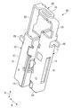
- a regulation protrusion 38 is formed around the insertion hole 33 corresponding to the guide 37. As shown in FIG. 1, the restricting protrusion 38 has a trapezoidal appearance.
- the restricting protrusion 38 is inserted into the guide 49 (FIG. 3) of the second housing 40.
- the regulation protrusion 38 is provided in a thin portion of the terminal holding floor 31.
- the terminal holding floor 31 provided with the insertion hole 32 is formed thick, but the insertion hole 33 is formed in relation to the second female terminal 12 being arranged at a position close to the circuit board 6.
- the thickness of the terminal holding floor 31 is reduced at the portion where the terminal is provided.
- This background is also related to the provision of the restricting projections 38 instead of increasing the thickness of the terminal holding floor 31.
- a peg 34 for fixing the first housing 30 to the first surface 7 of the circuit board 6 is provided on the surface of the terminal holding floor 31.
- the first housing 30 is fixed to the circuit board 6 by soldering the pegs 34 to the first surface 7.
- the housing recess 36 In the housing recess 36, the first male terminal 3 and the second male terminal 4 penetrating the terminal holding floor 31 and the female terminal 10 fitted thereto are accommodated.
- the housing recess 36 accommodates a second housing 40 and a third housing 50 that hold the female terminal 10, and these housings are fixed to the first housing 30.
- the second housing 40 includes a bottom floor 41 that faces the terminal holding floor 31 of the first housing 30, a side wall 45 that rises from the periphery of the bottom floor 41, and a bottom floor 41 and a side wall 45. And a partition 46 that divides the region surrounded by two into the receiving recesses 47 and 48.
- the bottom floor 41 is formed with an insertion hole 42 through which the first male terminal 3 is inserted and an insertion hole 43 through which the second male terminal 4 is inserted.
- the first male terminal 3 is loosely fitted in the insertion hole 42, and the second male terminal 4 is loosely fitted in the insertion hole 43.
- a guide 49 that is recessed in a taper shape around the insertion hole 43 is formed.
- the restriction protrusion 38 of the first housing 30 is inserted into the guide 49. Therefore, the invitation 49 has a space that can sufficiently accommodate the restricting protrusion 38.
- the first female terminal 11 is housed in the housing recess 47 and the second female terminal 12 is housed in the housing recess 48.
- the first female terminal 11 is held by the second housing 40 as one end (lower end) where the receiving port 14 is formed contacts the bottom floor 41 and the locking projection 18 is locked to the upper end of the side wall 45.
- the second female terminal 12 has one end (lower end) where the receiving port 14 is formed away from the bottom floor 41, and a play is provided between the side wall 45 and the partition 46 around the second female terminal 12.
- a gap is provided between the locking projection 18 of the second female terminal 12 and the upper end of the side wall 45 in contact with the housing recess 48. Therefore, the second female terminal 12 is suspended in the interior of the housing recess 48 via the connecting spring 20.
- the third housing 50 has a generally cap shape and includes a female terminal 10, a first male terminal 3, and a second male terminal 4.
- the first housing 30 is mounted so as to cover the upper portions of the first housing 30 and the second housing 40. Although illustration is omitted, the third housing 50 is detached from the first housing 30 by engaging the lock piece formed on the first housing 30 and the lock piece formed on the third housing 50. It has been stopped.
- the third housing 50 includes a ceiling 51, side walls 52 (52 ⁇ / b> A, 52 ⁇ / b> B) that hang down from the periphery of the ceiling 51, and an accommodation recess 53 that is surrounded by the ceiling 51 and the side walls 52.
- the lower end of the side wall 52 ⁇ / b> A contacts the locking protrusion 18 of the first female terminal 11. Accordingly, the first female terminal 11 is fixed to the housing 5 by the locking projection 18 being sandwiched from above and below by the side wall 45 of the second housing 40 and the side wall 52A of the third housing 50. Since the first housing 30 is fixed to the first surface 7 of the circuit board 6, the housing 5 is equivalent to the first female terminal 11 being fixed to the circuit board 6.
- a gap is provided between the lower end of the side wall 52B and the locking projection 18 of the second female terminal 12 with the third housing 50 mounted. Therefore, in this state, the locking projection 18 of the second female terminal 12 is not mechanically restrained.
- the coupling spring 20 is accommodated in the accommodating recess 53, but the ceiling 51 and the side wall 52 are provided along the coupling spring 20 with a small space therebetween.
- a pressing protrusion 54 that protrudes in the horizontal direction is formed on the ceiling 51 that intersects the side wall 52B. The pressing protrusion 54 is used when fitting the second male terminal 4 and the second female terminal 12 together.
- the electrical connector 1 can reduce the displacement of the second male terminal 4 by providing the terminal protrusion 31 with the restricting protrusion 38 on the terminal holding floor 31 of the first housing 30.
- the reason is as follows.
- the second male terminal 4 is loosely fitted in the insertion hole 33.
- Have difficulty If this inclination increases, the positional deviation at the desired contact between the second male terminal 4 and the second female terminal 12 increases, so it is necessary to reduce this inclination.
- the contact CP is normally determined at the design stage of the electrical connector 1.
- the first element is the length of the insertion hole 33 in the insertion / extraction direction
- the second element is the distance to the contact point between the second male terminal 4 and the second female terminal 12.
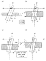
- FIG. 6 schematically showing the periphery of the insertion hole 33.
- 6A shows the case where the length of the insertion hole 33 in the insertion / extraction direction, in other words, the thickness of the terminal holding floor 31 around the insertion hole 33 is thin (t1)
- FIG. 6B shows the terminal holding floor 31. This shows a case where the thickness of (2) is large (t2).
- the second male terminal 4 to be inserted is shown as being inclined to the maximum inside the insertion hole 33.
- the contact between the second male terminal 4 and the second female terminal 12 is CP
- the positional deviation from the axial direction of the second male terminal 4 at the contact CP is apparent from FIGS. 6 (a) and 6 (b).
- the thickness of the terminal holding floor 31 is smaller in FIG. 6B (first element).
- the distance to the contact CP is different, as is clear from FIGS. 6C and 6D, the distance to the contact CP is shorter.
- the positional deviation from the axial direction of the second male terminal 4 at the contact CP is small (second element).
- providing the restricting protrusion 38 in addition to the invitation 37 means that the two elements are simultaneously provided. That is, compared with the case where the surface of the terminal holding floor 31 is kept flat without providing the restricting protrusion 38, the portion where the restricting protrusion 38 is provided is thicker in the terminal holding floor 31. With elements.
- a second element is provided since the distance from the end on the back side of the insertion hole 33 to the contact position is shortened by providing the restricting protrusion 38, a second element is provided.
- the electrical connector 1 can reduce the displacement of the second male terminal 4.
- the electrical connector 1 is formed with the restricting projection 38 only around the insertion hole 33, and the restricting projection 38 is inserted into the guide 49 of the second housing 40. Therefore, if the second housing 40 is also taken into consideration. The thickness of the housing 5 around the insertion hole 33 is not increased.
- the first female terminal 11 and the second female terminal 12 are arranged with their positions shifted in the insertion / extraction direction. By doing so, the timing at which the male terminal 3 is fitted to the first female terminal 11 and the timing at which the second male terminal 4 is fitted to the second female terminal 12 are shifted. Therefore, compared with the 1st female terminal 11 and the 2nd female terminal 12 being arrange
- the distance from the contact point between the main leaf 16 and the first male terminal 4 to the other end side of the second female terminal 12 is set as necessary. Since it can be made long, it is easy to ensure an effective contact length between the second male terminal 4 and the second female terminal 12.
- the electrical connector 1 has a trapezoidal appearance of the restricting projection 38, which is derived from the fact that the second male terminal 4 has a tab (flat) shape. Therefore, the appearance of the restriction protrusion can be specified according to the shape of the male terminal. For example, if the cross section of the male terminal is circular, the restriction protrusion forms a truncated cone.
- the electrical connector 1 includes a second housing 40 in which a guide 49 for accommodating the restriction protrusion 38 is formed, and further a third housing 50.
- the present invention can be applied to an electrical connector including only a housing corresponding to the first housing 30.
- the housing for accommodating the restricting protrusion 38 is not provided, but the restricting protrusion 38 exists only in a very limited range, so that it is hardly an obstacle to the assembly of the electrical connector with other members. .
- the configuration described in the above embodiment can be selected or changed to another configuration as appropriate.
Landscapes
- Coupling Device And Connection With Printed Circuit (AREA)
- Connector Housings Or Holding Contact Members (AREA)
Description
本発明は、相手側端子の誘い込みが形成されたハウジングを有する電気コネクタに関する。
電気コネクタ(以下、単にコネクタ)は、通常、オス型端子を保持するオスコネクタと、オス型端子と電気的に接続されるメス型端子を保持するメスコネクタとが互いに嵌合されている。
この嵌合を行なう際に、オス型端子が位置ずれすることなくメス型端子に接続、嵌合できることが、嵌合完了後のコネクタの信頼性を確保する上で必要である。そのために、オス型端子が貫通して挿入されるメスコネクタのハウジングに、誘い込みを設けることが行なわれている(例えば、特許文献1 図8)。誘い込みは、オス型端子が貫通するハウジングの挿通孔の周囲であって、オス型端子が挿入される側の面を、当該挿入の向きに先細りにしたテーパ形状に加工したものである。
この嵌合を行なう際に、オス型端子が位置ずれすることなくメス型端子に接続、嵌合できることが、嵌合完了後のコネクタの信頼性を確保する上で必要である。そのために、オス型端子が貫通して挿入されるメスコネクタのハウジングに、誘い込みを設けることが行なわれている(例えば、特許文献1 図8)。誘い込みは、オス型端子が貫通するハウジングの挿通孔の周囲であって、オス型端子が挿入される側の面を、当該挿入の向きに先細りにしたテーパ形状に加工したものである。
誘い込みを設けておくことにより、多少の位置ずれをしていても、オス型端子をハウジングの挿通孔に導くことができる。しかしながら、挿通孔の軸線に対してオス型端子が傾いて挿入されると、オス型端子が位置ずれを起したままでメス型端子に嵌合されるおそれがある。挿通孔との間のクリアランスを狭くすることにより、オス型端子の位置ずれを小さくできるが、ハウジングが樹脂を射出成形により作製されることを考慮すると限界がある。また、オス型端子が挿入される向きの挿通孔の長さ、換言すれば挿通孔を設けたハウジング壁の肉厚を厚くすれば、オス型端子の位置ずれを小さくできる。しかし、低背化に代表される小型化の要請が大きいコネクタにおいて、ハウジングのサイズを大きくすることに繋がるこの方策は適用が限定される。
本発明は、このような課題に基づいてなされたもので、ハウジングのサイズを大きくすることなく、相手側端子であるオス型端子の位置ずれを小さくできる電気コネクタを提供することを目的とする。
本発明は、このような課題に基づいてなされたもので、ハウジングのサイズを大きくすることなく、相手側端子であるオス型端子の位置ずれを小さくできる電気コネクタを提供することを目的とする。
本発明の電気コネクタは、相手側端子Yと電気的に接続される端子Xと、端子Xを保持し、電気的な接続がなされる際に相手側端子Yが挿入される挿通孔を有するハウジングと、を備える。このハウジングは、挿通孔の周囲であって、相手側端子Yが挿入される側の表面に形成される誘い込みと、表面に対向する裏面であって、誘い込みに対応して形成される規制突起と、備えることを特徴とする。
本発明の電気コネクタは、規制突起を誘い込みに対応してハウジングに形成するので、ハウジングの肉厚を厚くしたとしても限られた領域に留まるので、ハウジングのサイズを実質的に大きくすることがない。しかも、規制突起を設けることで、オス型端子の位置ずれを小さくできる。
本発明の電気コネクタは、規制突起を誘い込みに対応してハウジングに形成するので、ハウジングの肉厚を厚くしたとしても限られた領域に留まるので、ハウジングのサイズを実質的に大きくすることがない。しかも、規制突起を設けることで、オス型端子の位置ずれを小さくできる。
特にオス型端子の位置ずれを小さくする上で、本発明の電気コネクタにおいて、規制突起の頂点から、端子Xと相手側端子Yの接点までの距離をL1とし、規制突起の周囲の裏面から、接点までの距離をL2とすると、L1<L2を満たすことが好ましい。
本発明の電気コネクタにおいて、ハウジングが、外側に配置される第1ハウジングと、第1ハウジングよりも内側に配置される第2ハウジングと、を備えることがある。この場合、誘い込み及び規制突起が、第1ハウジングに形成され、規制突起を収容する凹部が、第2ハウジングに形成されることが好ましい。
本発明によれば、規制突起をハウジングに形成することで、ハウジングのサイズを大きくすることなく、オス型端子の位置ずれを小さくできる。
以下、添付する図1~5に示す電気コネクタ1に基づいてこの発明を詳細に説明する。
本実施の形態に係る電気コネクタ1は、メス型端子10と、メス型端子10を収容するハウジング5と、から構成される。メス型端子10は第1オス型端子3,第2オス型端子4と電気的に接続され、ハウジング5は回路基板6に固定される。第1オス型端子3は回路基板6に固定され、第2オス型端子4は、図中、回路基板6よりも下方に配置される他の機器に固定される。電気コネクタ1は、ハウジング5を構成する第1ハウジング30に形成される誘い込み37周囲の形状に特徴を有することにより、本発明の目的を達成する。以下、電気コネクタ1の各構成要素を順に説明する。
本実施の形態に係る電気コネクタ1は、メス型端子10と、メス型端子10を収容するハウジング5と、から構成される。メス型端子10は第1オス型端子3,第2オス型端子4と電気的に接続され、ハウジング5は回路基板6に固定される。第1オス型端子3は回路基板6に固定され、第2オス型端子4は、図中、回路基板6よりも下方に配置される他の機器に固定される。電気コネクタ1は、ハウジング5を構成する第1ハウジング30に形成される誘い込み37周囲の形状に特徴を有することにより、本発明の目的を達成する。以下、電気コネクタ1の各構成要素を順に説明する。
[メス型端子10]
メス型端子10は、図5に示すように、第1メス端子11と、第2メス端子12と、第1メス端子11と第2メス端子12とを繋ぐ連結バネ20とから構成される。メス型端子10は、銅、銅合金のように高導電性の金属板に切断及び折り曲げを施すことにより、第1メス端子11と、第2メス端子12と、連結バネ20とが、一体的に形成されている。ほぼ同じ形状及び寸法(仕様)に作製されている第1メス端子11と第2メス端子12は、第1オス型端子3,4との挿抜方向Aの位置をずらして、連結バネ20により繋がれている。
メス型端子10は、図5に示すように、第1メス端子11と、第2メス端子12と、第1メス端子11と第2メス端子12とを繋ぐ連結バネ20とから構成される。メス型端子10は、銅、銅合金のように高導電性の金属板に切断及び折り曲げを施すことにより、第1メス端子11と、第2メス端子12と、連結バネ20とが、一体的に形成されている。ほぼ同じ形状及び寸法(仕様)に作製されている第1メス端子11と第2メス端子12は、第1オス型端子3,4との挿抜方向Aの位置をずらして、連結バネ20により繋がれている。
第1メス端子11は、第1オス型端子3が挿入される受容口14が一端側に開口されたボックス状の端子本体13と、受容口14から挿入される第1オス型端子3を収容する受容キャビティ15と、を備える。端子本体13の他端側は、連結バネ20が一体的に接続されている。受容キャビティ15の内部には、図2に示される端子本体13の内壁に向けて挿入された第1オス型端子3を押し付ける主リーフ16と従リーフ17が設けられている。なお、図2において、主リーフ16は、第1オス型端子3が挿入されていない無負荷状態の位置に描かれているために、第1オス型端子3と重なっている。
端子本体13の外壁には、係止突起18が形成されている。係止突起18は、メス型端子10がハウジング5に装着された状態で、ハウジング5に係止されることでハウジング5に対するメス型端子10の位置決め及び抜け止めを担う。第2メス端子12は、第1メス端子11とほぼ同じ仕様を有しているため、第1メス端子11と同じ構成要素には同じ符号を付することで、その説明を省略する。ただし、メス型端子10がハウジング5に装着されると、第2メス端子12が第1メス端子11よりも回路基板6に近い位置に配置される。また、第2メス端子12の係止突起18は、後述するように、第1オス型端子3と第2メス端子12を嵌合させる際に機能する。
端子本体13の外壁には、係止突起18が形成されている。係止突起18は、メス型端子10がハウジング5に装着された状態で、ハウジング5に係止されることでハウジング5に対するメス型端子10の位置決め及び抜け止めを担う。第2メス端子12は、第1メス端子11とほぼ同じ仕様を有しているため、第1メス端子11と同じ構成要素には同じ符号を付することで、その説明を省略する。ただし、メス型端子10がハウジング5に装着されると、第2メス端子12が第1メス端子11よりも回路基板6に近い位置に配置される。また、第2メス端子12の係止突起18は、後述するように、第1オス型端子3と第2メス端子12を嵌合させる際に機能する。
第1メス端子11と第2メス端子12を繋ぐ連結バネ20は、一対の柱状部21,22と、柱状部21,22の先端同士を繋ぐ梁部23と、を備えている。柱状部21,22は、挿抜方向Aに沿って形成されているため、挿抜方向Aと直交する幅方向B(図1)に主に撓むことになる。梁部23は、S字状に形成することでバネ定数を小さくして、主に挿抜方向Aに容易に撓むことができる。メス型端子10がハウジング5に装着されると、第1メス端子11はハウジング5に対して固定、拘束されるが、第2メス端子12はハウジング5に拘束されずに自由状態となる。
[第1オス型端子3,第2オス型端子4]
タブ形状の第1オス型端子3,第2オス型端子4は、図2に示されるように、各々、第1メス端子11、第2メス端子12と嵌合される。
L字形状の第1オス型端子3は、回路基板6の第一面7に固定される。固定は、例えばはんだ付け(図示省略)により行なわれる。また、真直状の第2オス型端子4は、図示を省略する電気機器に固定される。
タブ形状の第1オス型端子3,第2オス型端子4は、図2に示されるように、各々、第1メス端子11、第2メス端子12と嵌合される。
L字形状の第1オス型端子3は、回路基板6の第一面7に固定される。固定は、例えばはんだ付け(図示省略)により行なわれる。また、真直状の第2オス型端子4は、図示を省略する電気機器に固定される。
第1オス型端子3は、その先端側が第1メス端子11の受容キャビティ15に挿入されることで、第1メス端子11と電気的に接続される。弾性変形する主リーフ16及び従リーフ17から押圧力を受ける第1オス型端子3は端子本体13の内壁に押し付けられることで、第1メス端子11と第1オス型端子3の電気的な接続が維持される。同様に、弾性変形する主リーフ16及び従リーフ17から押圧力を受ける第2オス型端子4は、端子本体13の内壁に押し付けられることで、第2メス端子12と第2オス型端子4の電気的な接続が維持される。回路基板6には表裏を貫通する挿通孔8が形成されており、第2オス型端子4はそこを通って受容キャビティ15に挿入される。
[ハウジング5]
ハウジング5は、図2,図3に示されるように、回路基板6上に固定され、かつ、メス型端子10を内部に収容する。
本実施形態におけるハウジング5は、第1ハウジング30、第2ハウジング40及び第3ハウジング50という3つの要素からなる。なお、ハウジング5は、回路基板6の側から、第1ハウジング30、第2ハウジング40及び第3ハウジング50の順に装着される。なお、これらのハウジング要素は、絶縁性の樹脂を射出成形することで作製される。
ハウジング5は、図2,図3に示されるように、回路基板6上に固定され、かつ、メス型端子10を内部に収容する。
本実施形態におけるハウジング5は、第1ハウジング30、第2ハウジング40及び第3ハウジング50という3つの要素からなる。なお、ハウジング5は、回路基板6の側から、第1ハウジング30、第2ハウジング40及び第3ハウジング50の順に装着される。なお、これらのハウジング要素は、絶縁性の樹脂を射出成形することで作製される。
[第1ハウジング30]
第1ハウジング30は、図1,2,4に示されるように、概ねキャップ(cap)を上下逆さまにした形状を有しており、回路基板6に対向する端子保持床31と、端子保持床31の周縁から立ち上る側壁35と、端子保持床31と側壁35に取り囲まれる収容凹部36と、を備えている。
第1ハウジング30は、図1,2,4に示されるように、概ねキャップ(cap)を上下逆さまにした形状を有しており、回路基板6に対向する端子保持床31と、端子保持床31の周縁から立ち上る側壁35と、端子保持床31と側壁35に取り囲まれる収容凹部36と、を備えている。
端子保持床31には、第1オス型端子3が挿通される挿通孔32と、第2オス型端子4が挿通される挿通孔33と、が形成されている。挿通孔32は、第1オス型端子3が圧入されるように、その開口寸法が設定される。一方、挿通孔33は、挿通される第2オス型端子4との間に遊び(クリアランス)を有するように、その開口寸法が設定される。なお、遊びを有して孔に挿通することを、以下では遊嵌と称する。第1オス型端子3が十分な力で端子保持床31に保持されるように、端子保持床31は、挿通孔32が形成される部分は挿通孔33が形成される部分よりも厚く形成されている。また、この厚さの差異は、第1メス端子11と第2メス端子12の位置ずれ量に対応している。
端子保持床31の表面には、挿通孔33の周囲がテーパ状に窪んだ誘い込み37が形成されている。第2オス型端子4をハウジング5に挿入するときに、その先端が誘い込み37のテーパ面に案内される。なお、端子保持床31の回路基板6に対向する側の面を表面とし、その反対側の面を裏面とする。第2ハウジング40についても同様である。
一方、端子保持床31の裏面には、挿通孔33の周囲に誘い込み37に対応して、規制突起38が形成されている。規制突起38は、図1に示すように、台形の外観を有している。第1ハウジング30と第2ハウジング40が組み付けられると、規制突起38は第2ハウジング40の誘い込み49(図3)の内部に挿入される。
ここで、規制突起38は、端子保持床31の中でも、肉厚の薄い部分に設けられている。挿通孔32が設けられる端子保持床31は肉厚が厚く形成されているが、第2メス端子12が回路基板6に近い位置に配置されることとの関係で、挿通孔33が形成されている部分は、端子保持床31の肉厚が薄くされている。端子保持床31の肉厚を厚くするのではなく、規制突起38を設けたのはこのような背景も関連している。
端子保持床31の表面には、挿通孔33の周囲がテーパ状に窪んだ誘い込み37が形成されている。第2オス型端子4をハウジング5に挿入するときに、その先端が誘い込み37のテーパ面に案内される。なお、端子保持床31の回路基板6に対向する側の面を表面とし、その反対側の面を裏面とする。第2ハウジング40についても同様である。
一方、端子保持床31の裏面には、挿通孔33の周囲に誘い込み37に対応して、規制突起38が形成されている。規制突起38は、図1に示すように、台形の外観を有している。第1ハウジング30と第2ハウジング40が組み付けられると、規制突起38は第2ハウジング40の誘い込み49(図3)の内部に挿入される。
ここで、規制突起38は、端子保持床31の中でも、肉厚の薄い部分に設けられている。挿通孔32が設けられる端子保持床31は肉厚が厚く形成されているが、第2メス端子12が回路基板6に近い位置に配置されることとの関係で、挿通孔33が形成されている部分は、端子保持床31の肉厚が薄くされている。端子保持床31の肉厚を厚くするのではなく、規制突起38を設けたのはこのような背景も関連している。
端子保持床31の表面には、第1ハウジング30を回路基板6の第一面7に固定するためのペグ34が設けられている。ペグ34を第一面7にはんだ付けすることにより、第1ハウジング30は回路基板6に固定される。
収容凹部36の内部には、端子保持床31を貫通する第1オス型端子3及び第2オス型端子4と、これらと嵌合されるメス型端子10と、が収容される。また、収容凹部36の内部には、メス型端子10を保持する第2ハウジング40と第3ハウジング50が収容され、これらハウジングは第1ハウジング30に対して固定される。
[第2ハウジング40]
第2ハウジング40は、図2,3に示されるように、第1ハウジング30の端子保持床31に対向する底床41と、底床41の周囲から立ち上る側壁45と、底床41と側壁45に取り囲まれる領域を2つの収容凹部47,48に区切る仕切り46と、を備えている。
底床41には、第1オス型端子3が挿通される挿通孔42と、第2オス型端子4が挿通される挿通孔43と、が形成されている。第1オス型端子3は挿通孔42に、また、第2オス型端子4は挿通孔43に、遊嵌される。
底床41の表面には、挿通孔43の周囲にテーパ状に窪んだ誘いこみ49が形成されている。誘い込み49の内部には、第1ハウジング30の規制突起38が挿入される。したがって、誘いこみ49は、規制突起38を十分に収容できるだけの空間を有している。規制突起38の表面と誘い込み49のテーパ面の間に隙間があるが、これは第1ハウジング30、第2ハウジング40を作製する際の寸法公差を考慮しているためであり、本発明を限定する要素にはならない。
第2ハウジング40は、図2,3に示されるように、第1ハウジング30の端子保持床31に対向する底床41と、底床41の周囲から立ち上る側壁45と、底床41と側壁45に取り囲まれる領域を2つの収容凹部47,48に区切る仕切り46と、を備えている。
底床41には、第1オス型端子3が挿通される挿通孔42と、第2オス型端子4が挿通される挿通孔43と、が形成されている。第1オス型端子3は挿通孔42に、また、第2オス型端子4は挿通孔43に、遊嵌される。
底床41の表面には、挿通孔43の周囲にテーパ状に窪んだ誘いこみ49が形成されている。誘い込み49の内部には、第1ハウジング30の規制突起38が挿入される。したがって、誘いこみ49は、規制突起38を十分に収容できるだけの空間を有している。規制突起38の表面と誘い込み49のテーパ面の間に隙間があるが、これは第1ハウジング30、第2ハウジング40を作製する際の寸法公差を考慮しているためであり、本発明を限定する要素にはならない。
収容凹部47には第1メス端子11が、また、収容凹部48には第2メス端子12が収容される。
第1メス端子11は、受容口14が形成される一端(下端)が底床41に接するとともに、係止突起18が側壁45の上端に係止されることで、第2ハウジング40に保持される。
一方、第2メス端子12は、受容口14が形成される一端(下端)が底床41から離れており、かつその周囲には側壁45及び仕切り46との間に遊びが設けられている。また、第2メス端子12の係止突起18は、収容凹部48に接する側壁45の上端との間に隙間が設けられている。したがって、第2メス端子12は連結バネ20を介して収容凹部48の内部に宙吊りにされている。
第1メス端子11は、受容口14が形成される一端(下端)が底床41に接するとともに、係止突起18が側壁45の上端に係止されることで、第2ハウジング40に保持される。
一方、第2メス端子12は、受容口14が形成される一端(下端)が底床41から離れており、かつその周囲には側壁45及び仕切り46との間に遊びが設けられている。また、第2メス端子12の係止突起18は、収容凹部48に接する側壁45の上端との間に隙間が設けられている。したがって、第2メス端子12は連結バネ20を介して収容凹部48の内部に宙吊りにされている。
[第3ハウジング50]
第3ハウジング50は、図2に示されるように、概ねキャップ(cap)状の形状を有しており、メス型端子10、第1オス型端子3、第2オス型端子4を含む、第1ハウジング30及び第2ハウジング40の上部を覆うように、第1ハウジング30に装着される。なお、図示は省略されているが、第1ハウジング30に形成されるロック片と第3ハウジング50に形成されるロック片が係合されることで、第3ハウジング50は第1ハウジング30から抜け止めされている。
第3ハウジング50は、図2に示されるように、概ねキャップ(cap)状の形状を有しており、メス型端子10、第1オス型端子3、第2オス型端子4を含む、第1ハウジング30及び第2ハウジング40の上部を覆うように、第1ハウジング30に装着される。なお、図示は省略されているが、第1ハウジング30に形成されるロック片と第3ハウジング50に形成されるロック片が係合されることで、第3ハウジング50は第1ハウジング30から抜け止めされている。
第3ハウジング50は、天井51と、天井51の周囲から垂れ下がる側壁52(52A,52B)と、天井51と側壁52に取り囲まれる収容凹部53と、を備えている。
第3ハウジング50が装着された状態で、側壁52Aは下端が第1メス端子11の係止突起18に接触する。したがって、第1メス端子11は、係止突起18が第2ハウジング40の側壁45と第3ハウジング50の側壁52Aにより上下から挟まれることで、ハウジング5に対して固定される。ハウジング5は第1ハウジング30が回路基板6の第一面7に固定されるので、第1メス端子11は回路基板6に固定されているのと等しい。
第3ハウジング50が装着された状態で、側壁52Aは下端が第1メス端子11の係止突起18に接触する。したがって、第1メス端子11は、係止突起18が第2ハウジング40の側壁45と第3ハウジング50の側壁52Aにより上下から挟まれることで、ハウジング5に対して固定される。ハウジング5は第1ハウジング30が回路基板6の第一面7に固定されるので、第1メス端子11は回路基板6に固定されているのと等しい。
一方、第3ハウジング50が装着された状態で、側壁52Bの下端と第2メス端子12の係止突起18との間に間隙が設けられている。したがって、この状態では、第2メス端子12の係止突起18は、機械的な拘束を受けない。
収容凹部53の内部には連結バネ20が収容されるが、天井51と側壁52は微小の間隔を隔てて連結バネ20に沿って設けられている。側壁52Bと交差する天井51には水平方向に突出する押圧突起54が形成されている。押圧突起54は、第2オス型端子4と第2メス端子12を嵌合させる際に用いる。
押圧突起54を下向きに押すと、天井51が反時計回りに撓むのに伴い、側壁52Bが下向きに変位して第2メス端子12の係止突起18に接触する。そこからさらに係止突起18を下向きに押すと、係止突起18が側壁45の上端に突き当たるまで変位する。このようにして第2メス端子12を一時的に拘束した状態で、第2オス型端子4と第2メス端子12の嵌合を確実に行なうことができる。この嵌合の作業が終わったならば、押圧突起54を押すのをやめて、第2メス端子12を機械的な拘束を受けない状態に戻す。
収容凹部53の内部には連結バネ20が収容されるが、天井51と側壁52は微小の間隔を隔てて連結バネ20に沿って設けられている。側壁52Bと交差する天井51には水平方向に突出する押圧突起54が形成されている。押圧突起54は、第2オス型端子4と第2メス端子12を嵌合させる際に用いる。
押圧突起54を下向きに押すと、天井51が反時計回りに撓むのに伴い、側壁52Bが下向きに変位して第2メス端子12の係止突起18に接触する。そこからさらに係止突起18を下向きに押すと、係止突起18が側壁45の上端に突き当たるまで変位する。このようにして第2メス端子12を一時的に拘束した状態で、第2オス型端子4と第2メス端子12の嵌合を確実に行なうことができる。この嵌合の作業が終わったならば、押圧突起54を押すのをやめて、第2メス端子12を機械的な拘束を受けない状態に戻す。
以上の構成を備える電気コネクタ1の作用・効果を以下説明する。
電気コネクタ1は、第1ハウジング30の端子保持床31に、誘い込み37に加えて規制突起38を設けることで、第2オス型端子4の位置ずれを小さくできる。理由は以下の通りである。
第2オス型端子4は挿通孔33に遊嵌される。その結果、誘い込み37に案内されたとしても、第2オス型端子4は、挿通孔33と同軸状に挿入されることは困難であり、挿通孔33を傾いて貫通することを回避することは困難である。この傾きが大きくなると第2オス型端子4と第2メス端子12との所望する接点において位置ずれが大きくなるので、この傾きを小さくすることが必要である。なお、接点CPは、通常、電気コネクタ1の設計段階で定まる。
電気コネクタ1は、第1ハウジング30の端子保持床31に、誘い込み37に加えて規制突起38を設けることで、第2オス型端子4の位置ずれを小さくできる。理由は以下の通りである。
第2オス型端子4は挿通孔33に遊嵌される。その結果、誘い込み37に案内されたとしても、第2オス型端子4は、挿通孔33と同軸状に挿入されることは困難であり、挿通孔33を傾いて貫通することを回避することは困難である。この傾きが大きくなると第2オス型端子4と第2メス端子12との所望する接点において位置ずれが大きくなるので、この傾きを小さくすることが必要である。なお、接点CPは、通常、電気コネクタ1の設計段階で定まる。
傾きを小さくする要素は少なくとも2つある。
一つ目の要素は挿通孔33の挿抜方向の長さであり、二つ目の要素は第2オス型端子4と第2メス端子12の接点までの距離である。以下、挿通孔33の周囲を模擬的に示す図6を参照して説明する。
図6(a)は挿通孔33の挿抜方向の長さ、換言すれば挿通孔33周囲の端子保持床31の厚さが薄い(t1)場合を、また図6(b)は端子保持床31の厚さが厚い(t2)場合を示している。図6(a),(b)ともに挿通される第2オス型端子4が挿通孔33の内部で最大に傾いたものとして示している。第2オス型端子4と第2メス端子12との接点をCPとすると、接点CPにおける第2オス型端子4の軸線方向から位置ずれは、図6(a),(b)から明らかなように、端子保持床31の厚さが厚い図6(b)の方が小さい(一つ目の要素)。
次に、端子保持床31の厚さは等しいが、接点CPまでの距離が相違する場合には、図6(c),(d)から明らかなように、接点CPまでの距離が短い方が、接点CPにおける第2オス型端子4の軸線方向からの位置ずれは小さい(二つ目の要素)。
一つ目の要素は挿通孔33の挿抜方向の長さであり、二つ目の要素は第2オス型端子4と第2メス端子12の接点までの距離である。以下、挿通孔33の周囲を模擬的に示す図6を参照して説明する。
図6(a)は挿通孔33の挿抜方向の長さ、換言すれば挿通孔33周囲の端子保持床31の厚さが薄い(t1)場合を、また図6(b)は端子保持床31の厚さが厚い(t2)場合を示している。図6(a),(b)ともに挿通される第2オス型端子4が挿通孔33の内部で最大に傾いたものとして示している。第2オス型端子4と第2メス端子12との接点をCPとすると、接点CPにおける第2オス型端子4の軸線方向から位置ずれは、図6(a),(b)から明らかなように、端子保持床31の厚さが厚い図6(b)の方が小さい(一つ目の要素)。
次に、端子保持床31の厚さは等しいが、接点CPまでの距離が相違する場合には、図6(c),(d)から明らかなように、接点CPまでの距離が短い方が、接点CPにおける第2オス型端子4の軸線方向からの位置ずれは小さい(二つ目の要素)。
本実施形態において、誘い込み37に加えて規制突起38を設けることは、二つの要素を同時に兼ね備えることを意味している。つまり、規制突起38を設けることなく端子保持床31の表面を偏平なままとした場合に比べると、規制突起38を設けた部分は端子保持床31の厚さが厚くなるので、一つ目の要素を備える。また、規制突起38を設けることにより、挿通孔33の裏側の端部から接点位置までの距離が短くなるので、二つ目の要素を備える。こうして、電気コネクタ1は、第2オス型端子4の位置ずれを小さくできる。しかも、電気コネクタ1は、挿通孔33の周囲にのみ規制突起38を形成しており、この規制突起38は第2ハウジング40の誘い込み49に挿入されるので、第2ハウジング40をも考慮すれば、挿通孔33の周囲のハウジング5の厚さを厚くすることにはならない。
以上が本実施形態の主要な効果であるが、以下の効果をも奏する。
電気コネクタ1は、第1メス端子11と第2メス端子12が、挿抜方向に位置がずれて配置される。
そうすることで、第1メス端子11にオス型端子3が嵌合されるタイミングと、第2メス端子12に第2オス型端子4が嵌合されるタイミングとがずれる。したがって、第1メス端子11と第2メス端子12が挿抜方向の同じ位置に配置されるのに比べて、同じ時点に必要な嵌合力を低減できる。
また、第1メス端子11と第2メス端子12を挿抜方向の位置をずらしているので、異なる長さの第1オス型端子3、第2オス型端子4を接続することができる。
さらに、回路基板6に近い側の第2メス端子12においては、主リーフ16と第1オス型端子4との接触点よりも第2メス端子12の他端側までの距離を必要に応じて長くできるので、第2オス型端子4と第2メス端子12における有効接触長を確保するのが容易である。
電気コネクタ1は、第1メス端子11と第2メス端子12が、挿抜方向に位置がずれて配置される。
そうすることで、第1メス端子11にオス型端子3が嵌合されるタイミングと、第2メス端子12に第2オス型端子4が嵌合されるタイミングとがずれる。したがって、第1メス端子11と第2メス端子12が挿抜方向の同じ位置に配置されるのに比べて、同じ時点に必要な嵌合力を低減できる。
また、第1メス端子11と第2メス端子12を挿抜方向の位置をずらしているので、異なる長さの第1オス型端子3、第2オス型端子4を接続することができる。
さらに、回路基板6に近い側の第2メス端子12においては、主リーフ16と第1オス型端子4との接触点よりも第2メス端子12の他端側までの距離を必要に応じて長くできるので、第2オス型端子4と第2メス端子12における有効接触長を確保するのが容易である。
以上、本発明を実施形態に基づいて説明したが、本発明は上記実施形態に限定されない。
本実施形態では、ボックス形状のメス型端子、タブ形状のオス型端子の例を示したが、他のタイプのメス型端子、オス型端子に本発明を適用することができる。
電気コネクタ1は、規制突起38の外観を台形としているが、これは第2オス型端子4がタブ(平形)形状であることに由来している。したがって、オス型端子の形状に応じて規制突起の外観を特定でき、例えば、断面が円形のオス型端子であれば、規制突起は円錐台をなすことになる。
また、電気コネクタ1は、規制突起38を備える第1ハウジング30の他に、規制突起38を収容する誘い込み49が形成された第2ハウジング40、さらには第3ハウジング50を備えるが、本発明は第1ハウジング30に相当するハウジングのみを備える電気コネクタに適用できる。この場合、規制突起38を収容するハウジングを有しないことになるが、規制突起38はごく限られた範囲にしか存在しないので、電気コネクタの他の部材との組み付けの障害になることはほとんどない。
これ以外にも、本発明の主旨を逸脱しない限り、上記実施の形態で挙げた構成を取捨選択したり、他の構成に適宜変更することが可能である。
本実施形態では、ボックス形状のメス型端子、タブ形状のオス型端子の例を示したが、他のタイプのメス型端子、オス型端子に本発明を適用することができる。
電気コネクタ1は、規制突起38の外観を台形としているが、これは第2オス型端子4がタブ(平形)形状であることに由来している。したがって、オス型端子の形状に応じて規制突起の外観を特定でき、例えば、断面が円形のオス型端子であれば、規制突起は円錐台をなすことになる。
また、電気コネクタ1は、規制突起38を備える第1ハウジング30の他に、規制突起38を収容する誘い込み49が形成された第2ハウジング40、さらには第3ハウジング50を備えるが、本発明は第1ハウジング30に相当するハウジングのみを備える電気コネクタに適用できる。この場合、規制突起38を収容するハウジングを有しないことになるが、規制突起38はごく限られた範囲にしか存在しないので、電気コネクタの他の部材との組み付けの障害になることはほとんどない。
これ以外にも、本発明の主旨を逸脱しない限り、上記実施の形態で挙げた構成を取捨選択したり、他の構成に適宜変更することが可能である。
1 電気コネクタ
3 第1オス型端子
4 第2オス型端子(相手側端子Y)
5 ハウジング
6 回路基板
7 第一面
8 挿通孔
10 メス型端子
11 第1メス端子
12 第2メス端子(端子X)
13 端子本体
14 受容口
15 受容キャビティ
16 主リーフ
17 従リーフ
18 係止突起
20 連結バネ
21,22 柱状部
23 梁部
30 第1ハウジング
31 端子保持床
32,33 挿通孔
34 ペグ
35 側壁
36 収容凹部
37 誘い込み
38 規制突起
40 第2ハウジング
41 底床
42 挿通孔
43 挿通孔
45 側壁
47,48 収容凹部
50 第3ハウジング
51 天井
52,52A,52B 側壁
53 収容凹部
54 押圧突起
CP 接点
3 第1オス型端子
4 第2オス型端子(相手側端子Y)
5 ハウジング
6 回路基板
7 第一面
8 挿通孔
10 メス型端子
11 第1メス端子
12 第2メス端子(端子X)
13 端子本体
14 受容口
15 受容キャビティ
16 主リーフ
17 従リーフ
18 係止突起
20 連結バネ
21,22 柱状部
23 梁部
30 第1ハウジング
31 端子保持床
32,33 挿通孔
34 ペグ
35 側壁
36 収容凹部
37 誘い込み
38 規制突起
40 第2ハウジング
41 底床
42 挿通孔
43 挿通孔
45 側壁
47,48 収容凹部
50 第3ハウジング
51 天井
52,52A,52B 側壁
53 収容凹部
54 押圧突起
CP 接点
Claims (5)
- 相手側端子Yに電気的な接続がなされる端子Xと、
前記端子Xを保持し、前記電気的な接続がなされる際に前記相手側端子Yが挿入される挿通孔を有するハウジングと、を備え、
前記ハウジングは、
前記挿通孔の周囲であって、前記相手側端子Yが挿入される側の表面に形成される誘い込みと、
前記表面に対向する裏面であって、前記誘い込みに対応して形成される規制突起と、備えることを特徴とする電気コネクタ。 - 前記規制突起の頂点から、前記端子Xと前記相手側端子Yの接点までの距離をL1とし、
前記規制突起の周囲の前記裏面から、前記接点までの距離をL2とすると、
L1<L2 を満たす、
請求項1に記載の電気コネクタ。 - 前記ハウジングは、
外側に配置される第1ハウジングと、
前記第1ハウジングよりも内側に配置される第2ハウジングと、を備え、
前記誘い込み及び前記規制突起が、前記第1ハウジングに形成され、
前記規制突起を収容する凹部が、前記第2ハウジングに形成される、
請求項1に記載の電気コネクタ。 - 前記相手側端子Yがタブ形状であり、
前記規制突起の外観が台形である、請求項1に記載の電気コネクタ。 - 前記挿通孔の周囲がテーパ状に窪むことにより、前記誘い込みが形成されている、請求項1に記載の電気コネクタ。
Applications Claiming Priority (2)
| Application Number | Priority Date | Filing Date | Title |
|---|---|---|---|
| JP2012-145263 | 2012-06-28 | ||
| JP2012145263A JP2014010951A (ja) | 2012-06-28 | 2012-06-28 | 電気コネクタ |
Publications (1)
| Publication Number | Publication Date |
|---|---|
| WO2014002501A1 true WO2014002501A1 (ja) | 2014-01-03 |
Family
ID=49782688
Family Applications (1)
| Application Number | Title | Priority Date | Filing Date |
|---|---|---|---|
| PCT/JP2013/004015 Ceased WO2014002501A1 (ja) | 2012-06-28 | 2013-06-27 | 電気コネクタ |
Country Status (2)
| Country | Link |
|---|---|
| JP (1) | JP2014010951A (ja) |
| WO (1) | WO2014002501A1 (ja) |
Citations (4)
| Publication number | Priority date | Publication date | Assignee | Title |
|---|---|---|---|---|
| JPH0227682U (ja) * | 1988-08-10 | 1990-02-22 | ||
| JP2006216308A (ja) * | 2005-02-02 | 2006-08-17 | Sumitomo Wiring Syst Ltd | コネクタ |
| JP2007005239A (ja) * | 2005-06-27 | 2007-01-11 | Sumitomo Wiring Syst Ltd | コネクタ |
| JP2011044291A (ja) * | 2009-08-20 | 2011-03-03 | Sumitomo Wiring Syst Ltd | コネクタ |
Family Cites Families (3)
| Publication number | Priority date | Publication date | Assignee | Title |
|---|---|---|---|---|
| JP3462096B2 (ja) * | 1998-11-05 | 2003-11-05 | 住友電装株式会社 | 基板用コネクタ |
| JP4175774B2 (ja) * | 2000-12-12 | 2008-11-05 | 矢崎総業株式会社 | コネクタ |
| JP3836755B2 (ja) * | 2002-06-19 | 2006-10-25 | 住友電装株式会社 | 電気接続箱 |
-
2012
- 2012-06-28 JP JP2012145263A patent/JP2014010951A/ja active Pending
-
2013
- 2013-06-27 WO PCT/JP2013/004015 patent/WO2014002501A1/ja not_active Ceased
Patent Citations (4)
| Publication number | Priority date | Publication date | Assignee | Title |
|---|---|---|---|---|
| JPH0227682U (ja) * | 1988-08-10 | 1990-02-22 | ||
| JP2006216308A (ja) * | 2005-02-02 | 2006-08-17 | Sumitomo Wiring Syst Ltd | コネクタ |
| JP2007005239A (ja) * | 2005-06-27 | 2007-01-11 | Sumitomo Wiring Syst Ltd | コネクタ |
| JP2011044291A (ja) * | 2009-08-20 | 2011-03-03 | Sumitomo Wiring Syst Ltd | コネクタ |
Also Published As
| Publication number | Publication date |
|---|---|
| JP2014010951A (ja) | 2014-01-20 |
Similar Documents
| Publication | Publication Date | Title |
|---|---|---|
| JP5964673B2 (ja) | 電気コネクタ及びメス型端子 | |
| JP6385815B2 (ja) | コネクタ組立体 | |
| JP6525221B2 (ja) | コネクタ | |
| JP5602617B2 (ja) | コネクタ部材 | |
| JP5955448B2 (ja) | コネクタ | |
| EP2903093A1 (en) | Electrical connector | |
| JP5947972B2 (ja) | 電子部品の組付構造及び電子部品 | |
| JP2015060628A (ja) | コネクタ | |
| WO2012095934A1 (en) | Terminal locking structure in connector housing | |
| JP5959719B2 (ja) | 電子部品の組付構造及び電気接続箱 | |
| CN107809037A (zh) | 电连接器以及电连接器组装体 | |
| CN110534951A (zh) | 连接器 | |
| JP2018181404A (ja) | 電気コネクタ | |
| JP2016054095A (ja) | コネクタ | |
| JP2018006246A (ja) | 端子モジュール、およびコネクタ | |
| JP2015099683A (ja) | コネクタ | |
| CN113675638A (zh) | 电路基板用电连接器 | |
| CN105281080A (zh) | 连接器端子和包括该连接器端子的连接器 | |
| JP2012243563A (ja) | コネクタ端子及びこのコネクタ端子を含むカードエッジ型コネクタ | |
| JPWO2014142250A1 (ja) | 電子部品の組付構造及び電気接続箱 | |
| JP2019053841A (ja) | コネクタ | |
| CN112018535A (zh) | 电连接器组装体 | |
| WO2014002501A1 (ja) | 電気コネクタ | |
| JP6746357B2 (ja) | コネクタ端子およびコネクタ | |
| JP5986912B2 (ja) | 端子 |
Legal Events
| Date | Code | Title | Description |
|---|---|---|---|
| 121 | Ep: the epo has been informed by wipo that ep was designated in this application |
Ref document number: 13809065 Country of ref document: EP Kind code of ref document: A1 |
|
| NENP | Non-entry into the national phase |
Ref country code: DE |
|
| 122 | Ep: pct application non-entry in european phase |
Ref document number: 13809065 Country of ref document: EP Kind code of ref document: A1 |