WO2013190895A1 - 半導体装置の製造方法および成膜装置 - Google Patents
半導体装置の製造方法および成膜装置 Download PDFInfo
- Publication number
- WO2013190895A1 WO2013190895A1 PCT/JP2013/061599 JP2013061599W WO2013190895A1 WO 2013190895 A1 WO2013190895 A1 WO 2013190895A1 JP 2013061599 W JP2013061599 W JP 2013061599W WO 2013190895 A1 WO2013190895 A1 WO 2013190895A1
- Authority
- WO
- WIPO (PCT)
- Prior art keywords
- film
- conductor film
- semiconductor device
- forming
- manufacturing
- Prior art date
- Legal status (The legal status is an assumption and is not a legal conclusion. Google has not performed a legal analysis and makes no representation as to the accuracy of the status listed.)
- Ceased
Links
Images







Classifications
-
- H—ELECTRICITY
- H10—SEMICONDUCTOR DEVICES; ELECTRIC SOLID-STATE DEVICES NOT OTHERWISE PROVIDED FOR
- H10P—GENERIC PROCESSES OR APPARATUS FOR THE MANUFACTURE OR TREATMENT OF DEVICES COVERED BY CLASS H10
- H10P74/00—Testing or measuring during manufacture or treatment of wafers, substrates or devices
- H10P74/23—Testing or measuring during manufacture or treatment of wafers, substrates or devices characterised by multiple measurements, corrections, marking or sorting processes
- H10P74/238—Testing or measuring during manufacture or treatment of wafers, substrates or devices characterised by multiple measurements, corrections, marking or sorting processes comprising acting in response to an ongoing measurement without interruption of processing, e.g. endpoint detection or in-situ thickness measurement
-
- H—ELECTRICITY
- H10—SEMICONDUCTOR DEVICES; ELECTRIC SOLID-STATE DEVICES NOT OTHERWISE PROVIDED FOR
- H10P—GENERIC PROCESSES OR APPARATUS FOR THE MANUFACTURE OR TREATMENT OF DEVICES COVERED BY CLASS H10
- H10P74/00—Testing or measuring during manufacture or treatment of wafers, substrates or devices
- H10P74/20—Testing or measuring during manufacture or treatment of wafers, substrates or devices characterised by the properties tested or measured, e.g. structural or electrical properties
- H10P74/207—Electrical properties, e.g. testing or measuring of resistance, deep levels or capacitance-voltage characteristics
-
- H—ELECTRICITY
- H10—SEMICONDUCTOR DEVICES; ELECTRIC SOLID-STATE DEVICES NOT OTHERWISE PROVIDED FOR
- H10W—GENERIC PACKAGES, INTERCONNECTIONS, CONNECTORS OR OTHER CONSTRUCTIONAL DETAILS OF DEVICES COVERED BY CLASS H10
- H10W72/00—Interconnections or connectors in packages
- H10W72/50—Bond wires
- H10W72/531—Shapes of wire connectors
- H10W72/536—Shapes of wire connectors the connected ends being ball-shaped
Definitions
- the present invention relates to a semiconductor device manufacturing method and a film forming apparatus, and more particularly, to a semiconductor device manufacturing method having a step of forming a conductor film, and a film forming apparatus for forming a conductor film. It is about.
- the manufacture of a semiconductor device usually involves the formation of a conductor film. In mass production, it is necessary to stably perform such film formation.
- a thin film is formed in the film forming chamber separately from the film forming sample. Further, a physical quantity measuring element that reads the physical quantity of the thin film during film formation, a comparison section that compares the physical quantity with a desired physical quantity, and a control section that controls film formation conditions based on the comparison result are provided.
- the present invention has been made to solve the above-described problems, and an object of the present invention is to manufacture a semiconductor device capable of feeding back the surface roughness of a film during film formation to film formation conditions.
- a method and a film forming apparatus therefor are provided.
- the method for manufacturing a semiconductor device of the present invention includes the following steps.
- a semiconductor substrate having a surface is prepared.
- a conductor film is formed on a region including the surface of the semiconductor substrate.
- the step of forming the conductor film includes the following steps. When the conductor film is partially formed, the characteristics regarding the AC loss and / or AC electrical conductivity of the partially formed conductor film are measured. Based on this characteristic, film forming conditions for forming the conductor film are adjusted.
- the surface roughness of the conductor film during film formation can be fed back to the film formation conditions. Thereby, a semiconductor device provided with a conductor film having a desired surface roughness is obtained.
- an alternating current having a frequency of 1 ⁇ 10 6 Hz or more and 1 ⁇ 10 15 Hz or less is applied to the partially formed conductor film.
- the conductor film may include a portion configured as a bonding pad for wire bonding.
- the bonding pad may be required to have a surface roughness of a certain level or more in order to secure the bonding strength with the bonding wire.
- the step of forming the conductor film may be performed by forming an aluminum film. Thereby, an aluminum film having a controlled surface roughness can be formed.
- the aluminum film can be used as a bonding pad, for example.
- the step of measuring the characteristics may include the following steps. An alternating current having a first frequency is applied to the partially formed conductor film. An alternating current having a second frequency different from the first frequency is applied to the partially formed conductor film.
- the film forming apparatus of the present invention includes a film forming unit, a measuring unit, and a control unit.
- the film forming unit is for forming a conductor film on a region including the surface of the semiconductor substrate.
- the measurement unit is for measuring characteristics related to at least one of AC loss and AC electrical conductivity and measuring the thickness of the conductor film on the region.
- the control unit is for adjusting the film forming conditions of the film forming unit based on the above characteristics.
- the surface roughness of the film being formed can be fed back to the film forming conditions. Thereby, a conductor film having a desired surface roughness can be formed.
- a conductor film having a desired surface roughness can be formed.
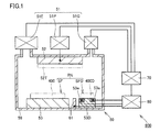
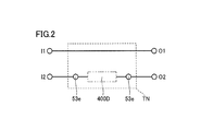
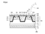
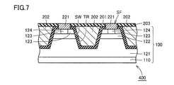
- FIG. 1 shows schematically the structure of the film-forming apparatus in Embodiment 1 of this invention. It is a circuit diagram for demonstrating schematically the measurement system of the measurement part in FIG. It is sectional drawing which shows schematically the 1st process of the manufacturing method of the semiconductor device in Embodiment 1 of this invention. It is sectional drawing which shows schematically the 2nd process of the manufacturing method of the semiconductor device in Embodiment 1 of this invention. It is sectional drawing which shows schematically the 3rd process of the manufacturing method of the semiconductor device in Embodiment 1 of this invention. It is a fragmentary sectional view which shows schematically the structure of the semiconductor device in Embodiment 2 of this invention.
- FIG. 1 shows schematically the structure of the semiconductor device in Embodiment 1 of this invention.
- FIG. 10 is a partial cross-sectional view schematically showing a tenth step of the method for manufacturing the semiconductor device in FIG. 6.
- FIG. 10 is a partial cross-sectional view schematically showing an eleventh step of the method for manufacturing the semiconductor device in FIG. 6.
- FIG. 7 is a partial cross sectional view schematically showing a first step of the method for manufacturing the semiconductor device of FIG. 6.
- FIG. 7 is a partial cross sectional view schematically showing a second step of the method for manufacturing the semiconductor device of FIG. 6.
- FIG. 7 is a partial cross-sectional view schematically showing a third step of the method for manufacturing the semiconductor device in FIG. 6.
- FIG. 7 is a partial cross-sectional view schematically showing a fourth step of the method for manufacturing the semiconductor device in FIG. 6.
- FIG. 10 is a partial cross-sectional view schematically showing a tenth step of the method for manufacturing the semiconductor device in FIG. 6.
- FIG. 10 is a partial cross-sectional view schematically showing an eleventh step of the
- FIG. 7 is a partial cross sectional view schematically showing a fifth step of the method for manufacturing the semiconductor device of FIG. 6.
- FIG. 7 is a partial cross-sectional view schematically showing a sixth step of the method for manufacturing the semiconductor device in FIG. 6.
- FIG. 7 is a partial cross-sectional view schematically showing a seventh step of the method for manufacturing the semiconductor device in FIG. 6.
- FIG. 10 is a partial cross-sectional view schematically showing an eighth step of the method for manufacturing the semiconductor device of FIG. 6.
- FIG. 10 is a partial cross-sectional view schematically showing a ninth step of the method for manufacturing the semiconductor device in FIG. 6.
- a film forming apparatus 900 of this embodiment is a sputter film forming apparatus for forming a conductor film.
- the conductor film refers to a film made of a conductor, and the conductor refers to a material having a conductivity of 1 ⁇ 10 ⁇ 6 (S / m) or more.
- the conductor is preferably a conductor.
- the film forming apparatus 900 includes a film forming unit 50, a measuring unit 60, and a control unit 70.
- the film forming unit 50 is for forming a conductor film on the region RN including the surface SF of the semiconductor substrate 400 and the surface SFD of the dummy 400D.
- the film forming unit 50 includes a controlled unit 51, a target mounting unit 52, a substrate support unit 53, a dummy support unit 53 ⁇ / b> D, and a container 59.
- the controlled unit 51 is capable of film formation under film formation conditions having film formation parameters that can be controlled from the outside.
- the controlled unit 51 includes a gas introduction unit 51G, an exhaust unit 51E, and a power source 51P.
- the gas introduction part 51G is for introducing a process gas into the container 59.
- the gas introduction part 51G has, for example, a gas type and a flow rate as film formation parameters.
- the exhaust part 51E is for exhausting gas from the container 59, and has, for example, a valve and a pump.
- the exhaust part 51E has, for example, a valve opening degree as a film formation parameter.
- the power source 51 ⁇ / b> P is for supplying power to the target mounting portion 52.
- the power source 51P has, for example, a power value as a film formation parameter.
- the target attachment portion 52 is configured to attach the sputtering target 52T.
- the substrate support 53 is for supporting the semiconductor substrate 400 having the surface SF.
- the substrate support 53 is, for example, a substrate stage provided with a chuck that can fix the semiconductor substrate 400.
- the dummy support portion 53D is for supporting the dummy 400D having the surface SFD.
- the dummy support portion 53D has a pair of electrodes 53e that are separated from each other. Each of the pair of electrodes 53e is disposed so as to contact the dummy 400D when the dummy 400D is supported.
- the measurement unit 60 is for measuring characteristics on at least one of AC loss and AC electrical conductivity on the surface SFD of the region RN. Measurement unit 60 may be able to measure a direct current characteristic on surface SFD of region RN. For these purposes, the measurement unit 60 is electrically connected to the pair of electrodes 53e of the dummy support unit 53D.
- the measurement unit 60 is, for example, an S parameter measurement system in an electric circuit TN (FIG. 2) having input terminals I1 and I2 and output terminals O1 and O2. The input terminal I1 and the output terminal O1 are short-circuited with each other.
- the input terminal I2 is connected to one of the pair of electrodes 53e, and the output terminal O2 is connected to the other of the pair of electrodes 53e.
- the S parameter can be measured by a network analyzer, for example.
- the measuring unit 60 is for measuring the thickness of the conductor film.
- the measurement unit 60 may be electrically connected to the film thickness measurement unit 61.
- the film thickness measuring unit 61 is, for example, a crystal resonator.
- the measurement part 60 is comprised so that a direct current measurement may also be performed as mentioned above, since the thickness of a conductor film can be calculated from this measurement result, the film thickness measurement part 61 can be abbreviate
- the control unit 70 is configured to control the film formation parameters of the controlled unit 51 based on the characteristics measured by the measurement unit 60. In other words, the control unit 70 is configured to be able to adjust the film forming conditions of the film forming unit 50.
- the control unit 70 is, for example, a computer that inputs information from the measurement unit 60 and outputs information to the controlled unit 51.
- FIGS. 3 to 5 a film forming method using the film forming apparatus 900 will be described with reference to FIGS.
- FIGS. 3 to 5 only a part of the film forming apparatus 900 (FIG. 1) is shown.
- This film forming method is applicable to a method for manufacturing a semiconductor device. Details of such application will be described in Embodiment 2.
- a semiconductor substrate 400 having a surface SF is prepared and supported by the substrate support portion 53.
- a dummy 400D is prepared and supported by the dummy support portion 53D.
- the dummy 400D has a pair of electrodes 400e separated from each other.
- One and the other of the pair of electrodes 400e are disposed so as to be in contact with one and the other of the pair of electrodes 53e.
- Each electrode 400e includes a portion on the surface SFD.
- the conductor film 222 (FIG. 5) is formed on the region RN including the surface SF of the semiconductor substrate 400 and the surface SFD of the dummy 400D through the process shown in FIG. Specifically, the following steps are performed.
- the control unit 70 controls the film formation parameters of the controlled unit 51 in accordance with a pre-programmed procedure, sputtering of the sputtering target 52T is started in a desired atmosphere.
- the formation of the conductor film is started on the region RN including the surface SF of the semiconductor substrate 400 and the surface SFD of the dummy 400D.
- the conductor film 222p is the one at the time when the conductor film 222 (FIG. 5) is partially formed (unfinished conductor film 222).
- the characteristics of the conductor film 222p relating to at least one of AC loss and AC electrical conductivity under a specific frequency are measured by the measurement unit 60 (FIG. 1).
- the thickness of the conductor film 222p is measured by the measuring unit 60. From the above characteristics and film thickness, the surface roughness of the surface SG of the conductor film 222p is estimated. This estimation method will be described below.
- the conductivity ⁇ C under a specific frequency of a portion formed between the pair of electrodes 400e in the conductor film 222p is calculated.
- the value of the following equation (1) can be obtained if the conductivity as the original physical property value of the material of the conductor film 222p is ⁇ .
- the value of ⁇ can be calculated from the film thickness and direct current characteristics measured by the measurement unit 60.
- the value of ⁇ may be treated as a known constant, and in this case, the direct current characteristics need not be measured.
- the surface roughness (RMS) of the surface SGD of the conductor film 222p can be estimated from the measured value of the formula (1) under a specific frequency, that is, the value of 1 / K W 2. . Since the surface SG is formed simultaneously with the surface SGD, it can be assumed that the surface roughness of the surface SG is approximately equal to the surface roughness of the surface SGD. Therefore, the surface roughness of the surface SG can be estimated.
- the control unit 70 compares the surface roughness estimated as described above with a desired surface roughness.
- the film forming conditions are adjusted according to the difference between the two. Specifically, when the estimated surface roughness is too small, the controlled unit 51 is controlled so that the surface roughness becomes larger by the subsequent film formation. On the other hand, if the estimated surface roughness is too large, the controlled portion 51 is controlled so that the surface roughness becomes smaller by subsequent film formation. As a result, a conductor film 222 (FIG. 5) provided with a surface SH having a desired surface roughness is finally formed.
- the surface roughness of the surface SG of the conductor film 222p (FIG. 4) being formed can be fed back to the film forming conditions.
- a semiconductor device including the conductor film 222 (FIG. 5) provided with the surface SH having a desired surface roughness can be manufactured.
- an alternating current having a frequency of 1 ⁇ 10 6 Hz or more and 1 ⁇ 10 15 Hz or less is preferably applied to the conductor film 222p.
- a frequency of 1 ⁇ 10 6 Hz or more it is possible to measure an RMS surface roughness of 10 ⁇ m or less which is particularly useful in a normal method for manufacturing a semiconductor device.
- the frequency is not excessively high by using a frequency of 1 ⁇ 10 15 Hz or less, the measurement unit of the film forming apparatus 900 can be simplified.
- an AC current having a first frequency is applied to the conductor film 222p, and a second different from the first frequency is applied to the conductor film 222p. It is preferable that an alternating current having a frequency is applied. Thereby, the surface roughness can be measured with higher accuracy or a wider range.
- a sputter film forming apparatus is used as the film forming apparatus.
- the film forming apparatus is not limited to the sputter film forming apparatus.
- a vapor deposition apparatus, a plating apparatus, or a CVD (Chemical Vapor Deposition) is used.
- CVD Chemical Vapor Deposition
- the measurement unit 60 measures the characteristics relating to at least one of AC loss and AC electrical conductivity on the surface SF instead of the surface SFD.
- the vertical MOSFET 500 semiconductor device
- the vertical MOSFET 500 semiconductor device
- the vertical MOSFET 500 semiconductor device
- the vertical MOSFET 500 semiconductor device
- the vertical MOSFET 500 semiconductor device
- the source wiring 222 is configured so that the bonding wire 300 can be bonded onto the surface SH thereof.
- the source wiring 222 includes a portion configured as a bonding pad for wire bonding.
- the source wiring 222 is preferably an aluminum film.
- Epitaxial substrate 100 has a single crystal substrate 110 and an epitaxial layer provided thereon.
- Single crystal substrate 110 has n-type (first conductivity type).
- the epitaxial layer has an n ⁇ layer 121 (first layer), a p-type body layer 122 (second layer), an n region 123 (third layer), and a contact region 124.
- N ⁇ layer 121 has n type (first conductivity type).
- the donor concentration of n ⁇ layer 121 is lower than the donor concentration of single crystal substrate 110.
- P-type body layer 122 is provided on n ⁇ layer 121 and has p-type (second conductivity type).
- N region 123 is provided on p type body layer 122.
- Contact region 124 has a p-type. Contact region 124 is formed on part of p type body layer 122 so as to be connected to p type body layer 122.
- Epitaxial substrate 100 has trench TR extending through n region 123 and p type body layer 122 to n ⁇ layer 121.
- Trench TR has a sidewall having surface SW.
- Surface SW includes a channel surface on p-type body layer 122.
- the gate oxide film 201 covers the trench TR. Specifically, gate oxide film 201 is provided on surface SW and bottom of trench TR. Gate oxide film 201 extends to the upper surface of n region 123. Gate electrode 202 is provided on gate oxide film 201 so as to fill the inside of trench TR. Gate electrode 202 faces surface SW of p-type body layer 122 with gate oxide film 201 interposed therebetween. The upper surface of the gate electrode 202 is substantially the same height as the upper surface of the portion of the gate oxide film 201 located on the upper surface of the n region 123. An interlayer insulating film 203 is provided so as to cover a portion of gate oxide film 201 that extends to the upper surface of n region 123 and gate electrode 202.
- Source electrode 221 is in contact with each of contact region 124 and n region 123.
- the source wiring 222 is in contact with the source electrode 221 and extends on the upper surface of the interlayer insulating film 203.
- Drain electrode 211 is an ohmic electrode provided on the back surface of single crystal substrate 110 opposite to the main surface on which n ⁇ layer 121 is provided.
- the protective electrode 212 is provided on the drain electrode 211.
- MOSFET 500 is obtained by forming drain electrode 211 and protective electrode 212.
- the surface roughness of the bonding pad made of the surface SH of the source wiring 222 can be made desired.
- the bonding pad may be required to have a surface roughness of a certain level or more in order to secure the bonding strength with the bonding wire 300.
- the surface roughness is extremely large, the bonding strength may be reduced due to the formation of a gap between the bonding wire 300 and the bonding pad. Therefore, from the viewpoint of bonding strength, it may be required that the surface roughness of the surface SH of the source wiring 222 be approximately a predetermined value.
- FIG. 7 a method for obtaining the semiconductor substrate 400 (FIG. 7) will be described below by taking as an example the case where the MOSFET (FIG. 6) is a silicon carbide semiconductor device.
- n ⁇ layer 121 is formed by epitaxial growth of silicon carbide on single crystal substrate 110 made of silicon carbide.
- This epitaxial growth is performed by a CVD (Chemical Vapor Deposition) method using, for example, a mixed gas of silane (SiH 4 ) and propane (C 3 H 8 ) as a source gas and using, for example, hydrogen gas (H 2 ) as a carrier gas.
- CVD Chemical Vapor Deposition
- SiH 4 silane
- propane C 3 H 8
- H 2 hydrogen gas
- n ⁇ layer 121 by performing ion implantation on the upper surface of n ⁇ layer 121, p type body layer 122, n region 123, and contact region 124 are formed.
- an impurity for imparting p-type such as aluminum (Al)
- Al aluminum
- ion implantation for forming n region 123 an impurity such as phosphorus (P) for imparting n-type is ion-implanted.
- epitaxial growth may be used instead of ion implantation.
- a mask layer 247 having an opening is formed on the surface composed of the n region 123 and the contact region 124.
- an insulating film such as a silicon oxide film can be used.
- the opening is formed at a position corresponding to the position of trench TR (FIG. 6).
- n region 123, p type body layer 122, and part of n ⁇ layer 121 are removed by etching in the opening of mask layer 247.
- etching method for example, reactive ion etching (RIE), particularly inductively coupled plasma (ICP) RIE can be used.
- ICP-RIE using SF 6 or a mixed gas of SF 6 and O 2 as a reaction gas can be used.
- recess TQ having an inner surface SV whose side wall is substantially perpendicular to the main surface of single crystal substrate 110 can be formed in a region where trench TR (FIG. 6) is to be formed.
- thermal etching is performed on the epitaxial substrate 100 on the inner surface SV of the recess TQ.
- the thermal etching can be performed, for example, by heating the epitaxial substrate 100 in an atmosphere containing a reactive gas having at least one kind of halogen atom.
- the at least one or more types of halogen atom includes at least one of a chlorine (Cl) atom and a fluorine (F) atom.
- This atmosphere is, for example, Cl 2 , BCL 3 , SF 6 , or CF 4 .
- thermal etching is performed using a mixed gas of chlorine gas and oxygen gas as a reaction gas and a heat treatment temperature of, for example, 700 ° C. or more and 1000 ° C. or less.
- trench TR is formed by thermal etching.
- surface SW having a portion formed of n ⁇ layer 121, p type body layer 122, and n region 123 is formed as a sidewall of trench TR.
- a specific crystal plane can be self-formed on the surface SW.
- the reaction gas may contain a carrier gas in addition to the above-described chlorine gas and oxygen gas.
- a carrier gas for example, nitrogen (N 2 ) gas, argon gas, helium gas or the like can be used.
- the SiC etching rate is, for example, about 70 ⁇ m / hour.
- the mask layer 247 made of silicon oxide has a very high selectivity with respect to SiC, so that it is not substantially etched during the etching of SiC.
- the mask layer 247 is removed by an arbitrary method such as etching (FIG. 14).
- activation annealing is performed to activate impurities implanted by ion implantation.
- a gate oxide film 201 is formed on the surface including the surface SW and the bottom which are the side walls of the trench TR.
- Gate oxide film 201 is obtained, for example, by thermally oxidizing an epitaxial layer made of silicon carbide.
- the gate electrode 202 is formed so as to fill the region inside the trench TR with the gate oxide film 201 interposed therebetween.
- the gate electrode 202 can be formed by, for example, film formation of a conductor and CMP (Chemical Mechanical Polishing).
- an interlayer insulating film 203 is formed on the gate electrode 202 and the gate oxide film 201 so as to cover the exposed surface of the gate electrode 202.
- etching is performed so that openings are formed in interlayer insulating film 203 and gate oxide film 201. By this opening, each of n region 123 and contact region 124 is exposed on the upper surface of the mesa structure.
- source electrode 221 in contact with each of n region 123 and contact region 124 is formed on the upper surface of the mesa structure. Thus, the semiconductor substrate 400 is obtained.
- the semiconductor device may be a MISFET (Metal Insulator Semiconductor Field Effect Transistor) other than a MOSFET.
- the semiconductor device is not limited to the MISFET, and may be, for example, an IGBT (Insulated Gate Bipolar Transistor).
- the semiconductor device is not limited to a transistor, and may be a diode, for example.
- the semiconductor device is not limited to the trench type, and may be a planar type, for example.
- the semiconductor device is not limited to a vertical type, and may be a horizontal type, for example.
Landscapes
- Electrodes Of Semiconductors (AREA)
- Testing Or Measuring Of Semiconductors Or The Like (AREA)
- Internal Circuitry In Semiconductor Integrated Circuit Devices (AREA)
- Physical Vapour Deposition (AREA)
Abstract
表面(SF)を有する半導体基板(400)が準備される。半導体基板(400)の表面(SF)を含む領域上に導電体膜が成膜される。導電体膜を成膜する工程は、次の工程を含む。導電体膜が部分的に形成された時点で、部分的に形成された導電体膜の、交流損失および交流電気伝導率の少なくともいずれかに関する特性が測定される。この特性に基づいて、導電体膜を成膜するための成膜条件が調整される。これにより、成膜中の膜の表面粗さを成膜条件へフィードバックすることができる。
Description
この発明は、半導体装置の製造方法および成膜装置に関するものであり、特に、導電体膜を成膜する工程を有する半導体装置の製造方法と、導電体膜を成膜するための成膜装置とに関するものである。
半導体装置の製造は、通常、導電体膜の成膜をともなう。量産においては、このような成膜を安定的に行う必要がある。特開2010-236040号公報(特許文献1)の成膜装置によれば、成膜チャンバ内に成膜サンプルとは別に薄膜が成膜される。また、成膜中薄膜の物理量を読み取る物理量測定素子と、その物理量と所望の物理量とを比較する比較部と、比較結果に基づいて成膜条件などを制御する制御部とが設けられる。
成膜条件へフィードバックするパラメータとして成膜中の膜の表面粗さを用いることができる簡素な方法は、これまで知られていなかった。
本発明は、上記のような課題を解決するために成されたものであり、この発明の目的は、成膜中の膜の表面粗さを成膜条件へフィードバックすることができる半導体装置の製造方法と、そのための成膜装置とを提供することである。
本発明の半導体装置の製造方法は、以下の工程を有する。
表面を有する半導体基板が準備される。半導体基板の表面を含む領域上に導電体膜が成膜される。導電体膜を成膜する工程は、次の工程を含む。導電体膜が部分的に形成された時点で、部分的に形成された導電体膜の、交流損失および交流電気伝導率の少なくともいずれかに関する特性が測定される。この特性に基づいて、導電体膜を成膜するための成膜条件が調整される。
表面を有する半導体基板が準備される。半導体基板の表面を含む領域上に導電体膜が成膜される。導電体膜を成膜する工程は、次の工程を含む。導電体膜が部分的に形成された時点で、部分的に形成された導電体膜の、交流損失および交流電気伝導率の少なくともいずれかに関する特性が測定される。この特性に基づいて、導電体膜を成膜するための成膜条件が調整される。
この製造方法によれば、成膜中の導電体膜の表面粗さを成膜条件へフィードバックすることができる。これにより、所望の表面粗さを有する導電体膜が設けられた半導体装置が得られる。
特性が測定される際に、部分的に形成された導電体膜に1×10⁶Hz以上1×10¹⁵Hz以下の周波数を有する交流電流が印加されることが好ましい。
1×10⁶Hz以上の周波数が用いられることで、通常の半導体装置の製造方法において特に有用な10μm以下のRMS表面粗さを測定することができる。また1×10¹⁵Hz以下の周波数が用いられることで、周波数が過度に高くなくなるので、成膜装置の測定部を簡素なものとすることができる。
導電体膜はワイヤボンディングのボンディングパッドとして構成された部分を含んでもよい。
これによりボンディングパッドの表面粗さを所望のものとすることができる。なおボンディングパッドは、ボンディングワイヤとの接合強度を確保する上で、ある程度以上の表面粗さを有することが求められる場合がある。
導電体膜を成膜する工程は、アルミニウム膜を成膜することによって行われてもよい。
これにより、表面粗さが管理されたアルミニウム膜を成膜することができる。アルミニウム膜は、たとえばボンディングパッドとして用いることができる。
これにより、表面粗さが管理されたアルミニウム膜を成膜することができる。アルミニウム膜は、たとえばボンディングパッドとして用いることができる。
特性を測定する工程は、次の工程を含んでもよい。部分的に形成された導電体膜に、第1の周波数を有する交流電流が印加される。部分的に形成された導電体膜に、第1の周波数と異なる第2の周波数を有する交流電流が印加される。
これにより、より高い精度またはより広いレンジで、表面粗さを測定することができる。
本発明の成膜装置は、成膜部と、測定部と、制御部とを有する。成膜部は、半導体基板の表面を含む領域上に導電体膜を成膜するためのものである。測定部は、上記領域上において、交流損失および交流電気伝導率の少なくともいずれかに関する特性を測定しかつ、導電体膜の厚さを測定するためのものである。制御部は、上記特性に基づいて成膜部の成膜条件を調整するためのものである。
この成膜装置によれば、成膜中の膜の表面粗さを成膜条件へフィードバックすることができる。これにより、所望の表面粗さを有する導電体膜を成膜することができる。
上記のように本発明によれば、所望の表面粗さを有する導電体膜を成膜することができる。
以下、本発明の実施の形態について図に基づいて説明する。なお、以下の図面において、同一または相当する部分には同一の参照番号を付し、その説明は繰り返さない。また、本明細書中の結晶学的記載においては、個別方位を[]、集合方位を<>、個別面を()、集合面を{}でそれぞれ示している。また結晶学上の指数が負であることは、通常、”-”(バー)を数字の上に付すことによって表現されるが、本明細書中では数字の前に負の符号を付している。
(実施の形態1)
図1に示すように、本実施の形態の成膜装置900は、導電体膜を成膜するためのスパッタ成膜装置である。ここで導電体膜とは導電体から作られた膜のことをいい、導電体とは1×10⁻⁶(S/m)以上の伝導率を有する材料をいう。導電体は、好ましくは導体である。成膜装置900は、成膜部50と、測定部60と、制御部70とを有する。
図1に示すように、本実施の形態の成膜装置900は、導電体膜を成膜するためのスパッタ成膜装置である。ここで導電体膜とは導電体から作られた膜のことをいい、導電体とは1×10⁻⁶(S/m)以上の伝導率を有する材料をいう。導電体は、好ましくは導体である。成膜装置900は、成膜部50と、測定部60と、制御部70とを有する。
成膜部50は、半導体基板400の表面SFと、ダミー400Dの表面SFDとを含む領域RN上に、導電体膜を成膜するためのものである。具体的には、成膜部50は、被制御部51と、ターゲット取付部52と、基板支持部53と、ダミー支持部53Dと、容器59とを有する。
被制御部51は、外部から制御可能な成膜パラメータを有する成膜条件下での成膜を可能とするものである。具体的には被制御部51は、ガス導入部51Gと、排気部51Eと、電源51Pとを有する。ガス導入部51Gは、容器59内にプロセスガスを導入するためのものである。ガス導入部51Gは成膜パラメータとして、たとえばガス種および流量を有する。排気部51Eは、容器59からガスを排気するためのものであり、たとえばバルブとポンプとを有する。排気部51Eは成膜パラメータとして、たとえばバルブの開口度を有する。電源51Pは、ターゲット取付部52へ電力を供給するためのものである。電源51Pは成膜パラメータとして、たとえば電力値を有する。ターゲット取付部52は、スパッタリングターゲット52Tが取り付けられるように構成されている。
基板支持部53は、表面SFを有する半導体基板400を支持するためのものである。基板支持部53は、たとえば、半導体基板400を固定することができるチャックが設けられた基板ステージである。
ダミー支持部53Dは、表面SFDを有するダミー400Dを支持するためのものである。ダミー支持部53Dは、互いに離れた1対の電極53eを有する。1対の電極53eの各々は、ダミー400Dが支持された際にダミー400Dに接触するように配置されている。
測定部60は、領域RNの表面SFD上において、交流損失および交流電気伝導率の少なくともいずれかに関する特性を測定するためのものである。また測定部60は、領域RNの表面SFD上において、直流電流特性を測定することができてもよい。これらの目的で、測定部60は、ダミー支持部53Dの1対の電極53eに電気的に接続されている。測定部60は、たとえば、入力端子I1およびI2と、出力端子O1およびO2とを有する電気回路TN(図2)におけるSパラメータの測定系である。入力端子I1と出力端子O1とは互いに短絡されている。入力端子I2は1対の電極53eの一方に接続されており、出力端子O2は1対の電極53eの他方に接続されている。Sパラメータの測定は、たとえばネットワークアナライザにより行うことができる。
また測定部60は、導電体膜の厚さを測定するためのものである。この目的で、測定部60は、膜厚測定部61に電気的に接続されていてもよい。膜厚測定部61は、たとえば水晶振動子である。なお測定部60が、上述したように直流電流測定も行うように構成されている場合、この測定結果から導電体膜の厚さを算出することができるので、膜厚測定部61は省略され得る。
制御部70は、測定部60によって測定された特性に基づいて、被制御部51の成膜パラメータを制御することができるように構成されている。言い換えれば、制御部70は、成膜部50の成膜条件を調整することができるように構成されている。制御部70は、たとえば、測定部60からの情報の入力と、被制御部51への情報の出力とを行うコンピュータである。
次に成膜装置900を用いた成膜方法について、図3~図5を用いて説明する。なお図3~図5の各々においては、成膜装置900(図1)についてその一部のみが示されている。またこの成膜方法は、半導体装置の製造方法に適用可能である。そのような適用についての詳細は、実施の形態2において説明する。
図3を参照して、表面SFを有する半導体基板400が準備され、基板支持部53に支持される。またダミー400Dが準備され、ダミー支持部53Dに支持される。ダミー400Dは、互いに離れた1対の電極400eを有する。1対の電極400eの一方および他方のそれぞれは、1対の電極53eの一方および他方に接触することができるように配置されている。また各電極400eは表面SFD上の部分を含む。
次に、図4に示す工程を経て、半導体基板400の表面SFと、ダミー400Dの表面SFDとを含むを含む領域RN上に、導電体膜222(図5)が成膜される。具体的には、以下の工程が行われる。
たとえば、予めプログラムされた手順に沿って制御部70が被制御部51の成膜パラメータを制御することで、所望の雰囲気中で、スパッタリングターゲット52Tのスパッタが開始される。これにより図4に示すように、半導体基板400の表面SFと、ダミー400Dの表面SFDとを含む領域RN上において、導電体膜の成膜が開始される。図4において導電体膜222pは、導電体膜222(図5)が部分的に形成された時点のもの(未完成の導電体膜222)である。この時点で、導電体膜222pの、特定の周波数の下での交流損失および交流電気伝導率の少なくともいずれかに関する特性が、測定部60(図1)により測定される。また導電体膜222pの膜厚が測定部60により測定される。上記特性および膜厚から、導電体膜222pの表面SGの表面粗さが見積もられる。この見積もりの方法について、以下に説明する。
まず、測定された上記特性および膜厚に基づいて、導電体膜222pのうち1対の電極400e間に形成された部分の、特定の周波数の下での伝導率σCが算出される。これにより、導電体膜222pの材料本来の物性値としての伝導率をσとすれば、下記の式(1)の値が分かる。
1/KW
2=σC/σ ・・・(1)
なおσの値は、測定部60によって測定された、膜厚および直流電流特性から算出され得る。またはσの値は、既知の定数として扱われてもよく、この場合は直流電流特性の測定は行われなくてもよい。
なおσの値は、測定部60によって測定された、膜厚および直流電流特性から算出され得る。またはσの値は、既知の定数として扱われてもよく、この場合は直流電流特性の測定は行われなくてもよい。
一方、表皮効果における表皮深さをs、導電体膜222pのうちダミー400D上の部分の表面SGD(図4)の表面粗さ(RMS)をhとすると、以下の式(2)が成り立つ。
KW=1+exp(-s/2h)1.6 ・・・(2)
表皮深さsは、周波数角速度をω、透磁率をμとすれば、以下の(3)式で表される。
表皮深さsは、周波数角速度をω、透磁率をμとすれば、以下の(3)式で表される。
s={2/(σ・ω・μ)}0.5 ・・・(3)
導電体膜222pがアルミニウムからなる場合、sは、下記の表1に示すように周波数に依存する。
導電体膜222pがアルミニウムからなる場合、sは、下記の表1に示すように周波数に依存する。

上記の(2)式および表1から、表面粗さ(RMS)および周波数(f)の組み合わせに対応した1/KW
2の値が、以下の表2に示すように算出される。

上記の表2により、特定の周波数の下での式(1)の測定値、すなわち1/KW
2の値から、導電体膜222pの表面SGDの表面粗さ(RMS)を見積もることができる。表面SGは表面SGDと同時に形成されることから、表面SGの表面粗さは、表面SGDの表面粗さとおおよそ等しいと想定することができる。よって表面SGの表面粗さを見積もることができる。
制御部70は、上記のようにして見積もられた表面粗さと、所望の表面粗さとの比較を行う。そして両者の相違に応じて成膜条件が調整される。具体的には、見積もられた表面粗さが小さ過ぎる場合は、以後の成膜によって表面粗さがより大きくなるように被制御部51が制御される。逆に、見積もられた表面粗さが大き過ぎる場合は、以後の成膜によって表面粗さがより小さくなるように被制御部51が制御される。これにより、最終的に所望の表面粗さを有する表面SHが設けられた導電体膜222(図5)が成膜される。
本実施の形態によれば、成膜中の導電体膜222p(図4)の表面SGの表面粗さを成膜条件へフィードバックすることができる。これにより、所望の表面粗さを有する表面SHが設けられた導電体膜222(図5)を含む半導体装置を製造することができる。
測定部60によって特性が測定される際には、導電体膜222pに1×10⁶Hz以上1×10¹⁵Hz以下の周波数を有する交流電流が印加されることが好ましい。1×10⁶Hz以上の周波数が用いられることで、通常の半導体装置の製造方法において特に有用な10μm以下のRMS表面粗さを測定することができる。また1×10¹⁵Hz以下の周波数が用いられることで、周波数が過度に高くなくなるので、成膜装置900の測定部を簡素なものとすることができる。
また測定部60によって特性が測定される際には、導電体膜222pに、第1の周波数を有する交流電流が印加される工程と、導電体膜222pに、第1の周波数と異なる第2の周波数を有する交流電流が印加される工程とが行われることが好ましい。これにより、より高い精度またはより広いレンジで、表面粗さを測定することができる。
なお本実施の形態においては成膜装置としてスパッタ成膜装置が用いられるが、成膜装置はスパッタ成膜装置に限定されるものではなく、たとえば、蒸着装置、めっき装置、またはCVD(Chemical Vapor Deposition)装置であってもよい。
またダミー400Dが用いられる代わりに、同様の構成が半導体基板400上にTEG(テストエレメントグループ(Test Element Group))として設けられてもよい。この場合、測定部60は、交流損失および交流電気伝導率の少なくともいずれかに関する特性を測定を、表面SFDの代わりに表面SF上において行う。
(実施の形態2)
図6に示すように、本実施の形態の縦型MOSFET500(半導体装置)は、エピタキシャル基板100と、ゲート酸化膜201(ゲート絶縁膜)と、ゲート電極202と、層間絶縁膜203と、ソース電極221と、ドレイン電極211と、ソース配線222(導電体膜)と、保護電極212とを有する。ソース配線222は、その表面SH上にボンディングワイヤ300を接合することができるように構成されている。言い換えれば、ソース配線222は、ワイヤボンディングのボンディングパッドとして構成された部分を含んでいる。ソース配線222は、好ましくはアルミニウム膜である。
図6に示すように、本実施の形態の縦型MOSFET500(半導体装置)は、エピタキシャル基板100と、ゲート酸化膜201(ゲート絶縁膜)と、ゲート電極202と、層間絶縁膜203と、ソース電極221と、ドレイン電極211と、ソース配線222(導電体膜)と、保護電極212とを有する。ソース配線222は、その表面SH上にボンディングワイヤ300を接合することができるように構成されている。言い換えれば、ソース配線222は、ワイヤボンディングのボンディングパッドとして構成された部分を含んでいる。ソース配線222は、好ましくはアルミニウム膜である。
エピタキシャル基板100は、単結晶基板110と、その上に設けられたエピタキシャル層とを有する。単結晶基板110はn型(第1の導電型)を有する。エピタキシャル層は、n-層121(第1の層)と、p型ボディ層122(第2の層)と、n領域123(第3の層)と、コンタクト領域124とを有する。n-層121はn型(第1の導電型)を有する。n-層121のドナー濃度は、単結晶基板110のドナー濃度よりも低い。p型ボディ層122は、n-層121上に設けられており、p型(第2の導電型)を有する。n領域123は、p型ボディ層122上に設けられている。コンタクト領域124はp型を有する。コンタクト領域124は、p型ボディ層122につながるようにp型ボディ層122の一部の上に形成されている。
エピタキシャル基板100は、n領域123およびp型ボディ層122を貫通してn-層121に至るトレンチTRを有する。トレンチTRは表面SWを有する側壁を有する。表面SWはp型ボディ層122上においてチャネル面を含む。
ゲート酸化膜201はトレンチTRを被覆している。具体的にはトレンチTRの表面SW上および底部上にゲート酸化膜201が設けられている。このゲート酸化膜201はn領域123の上面上にまで延在している。ゲート電極202は、トレンチTRの内部を充填するように、ゲート酸化膜201上に設けられている。ゲート電極202はゲート酸化膜201を介してp型ボディ層122の表面SWに対向している。ゲート電極202の上面は、ゲート酸化膜201のうちn領域123の上面上に位置する部分の上面とほぼ同じ高さになっている。ゲート酸化膜201のうちn領域123の上面上にまで延在する部分とゲート電極202とを覆うように、層間絶縁膜203が設けられている。
ソース電極221はコンタクト領域124およびn領域123の各々に接触している。ソース配線222はソース電極221に接触しており、層間絶縁膜203の上面上に延在している。ドレイン電極211は、単結晶基板110においてn-層121が設けられた主表面とは反対側の裏面上に設けられたオーミック電極である。保護電極212はドレイン電極211上に設けられている。
次にMOSFET500の製造方法について説明する。図7を参照して、後述する方法によって半導体基板400が準備される。半導体基板400は、層間絶縁膜203およびソース電極221からなる表面SFを有する。さらに図8を参照して、実施の形態1で説明した成膜方法によって、表面SF上に、表面SHを有するソース配線222が成膜される。再び図6を参照して、ドレイン電極211および保護電極212が形成されることで、MOSFET500が得られる。
本実施の形態によれば、ソース配線222の表面SHからなるボンディングパッドの表面粗さを所望のものとすることができる。なおボンディングパッドは、ボンディングワイヤ300との接合強度を確保する上で、ある程度以上の表面粗さを有することが求められる場合がある。ただし極端に表面粗さが大きいと、ボンディングワイヤ300とボンディングパッドとの間に空隙が形成されることで接合強度が逆に低下してしまうことがあり得る。よって接合強度の観点で、ソース配線222の表面SHの表面粗さをおおよそ所定の値とすることが求められる場合がある。
次に、MOSFET(図6)が炭化珪素半導体装置である場合を例に、半導体基板400(図7)を得るまでの方法について、以下に説明する。
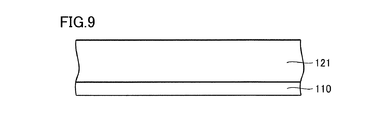
図9に示すように、炭化珪素から作られた単結晶基板110上における炭化珪素のエピタキシャル成長によってn-層121が形成される。このエピタキシャル成長は、たとえば原料ガスとしてシラン(SiH4)とプロパン(C3H8)との混合ガスを用い、キャリアガスとしてたとえば水素ガス(H2)を用いたCVD(Chemical Vapor Deposition)法により行うことができる。また、このとき導電型がn型の不純物としてたとえば窒素(N)やリン(P)を導入することが好ましい。
図10に示すように、n-層121の上面にイオン注入を行うことにより、p型ボディ層122と、n領域123と、コンタクト領域124とが形成される。p型ボディ層122およびコンタクト領域124を形成するためのイオン注入においては、たとえばアルミニウム(Al)などの、p型を付与するための不純物がイオン注入される。またn領域123を形成するためのイオン注入においては、たとえばリン(P)などの、n型を付与するための不純物がイオン注入される。なおイオン注入の代わりにエピタキシャル成長が用いられてもよい。
図11に示すように、n領域123およびコンタクト領域124からなる面上に、開口部を有するマスク層247が形成される。マスク層247として、たとえばシリコン酸化膜などの絶縁膜を用いることができる。開口部は、トレンチTR(図6)の位置に対応する位置に形成される。
図12に示すように、マスク層247の開口部において、n領域123と、p型ボディ層122と、n-層121の一部とがエッチングにより除去される。エッチングの方法としては、たとえば反応性イオンエッチング(RIE)、特に誘導結合プラズマ(ICP)RIEを用いることができる。具体的には、たとえば反応ガスとしてSF6またはSF6とO2との混合ガスを用いたICP-RIEを用いることができる。このようなエッチングにより、トレンチTR(図6)が形成されるべき領域に、側壁が単結晶基板110の主表面に対してほぼ垂直な内面SVを有する凹部TQを形成することができる。
次に、エピタキシャル基板100に対して、凹部TQの内面SVにおいて、熱エッチングが行われる。熱エッチングは、たとえば、少なくとも1種類以上のハロゲン原子を有する反応性ガスを含む雰囲気中で、エピタキシャル基板100を加熱することによって行い得る。少なくとも1種類以上のハロゲン原子は、塩素(Cl)原子およびフッ素(F)原子の少なくともいずれかを含む。この雰囲気は、たとえば、Cl2、BCL3、SF6、またはCF4である。たとえば、塩素ガスと酸素ガスとの混合ガスを反応ガスとして用い、熱処理温度を、たとえば700℃以上1000℃以下として、熱エッチングが行われる。
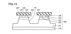
図13に示すように、熱エッチングによりトレンチTRが形成される。この際、トレンチTRの側壁として、n-層121、p型ボディ層122およびn領域123の各々からなる部分を有する表面SWが形成される。表面SW上においては特定の結晶面が自己形成され得る。
なお、反応ガスは、上述した塩素ガスと酸素ガスとに加えて、キャリアガスを含んでいてもよい。キャリアガスとしては、たとえば窒素(N2)ガス、アルゴンガス、ヘリウムガスなどを用いることができる。そして、上述のように熱処理温度を700℃以上1000℃以下とした場合、SiCのエッチング速度はたとえば約70μm/時になる。また、この場合に、酸化珪素から作られたマスク層247は、SiCに対する選択比が極めて大きいので、SiCのエッチング中に実質的にエッチングされない。
次にマスク層247がエッチングなど任意の方法により除去される(図14)。またイオン注入により注入された不純物を活性化するための活性化アニールが行われる。
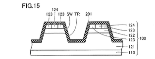
図15に示すように、トレンチTRの側壁である表面SWと底部とを含む面上にゲート酸化膜201が形成される。ゲート酸化膜201は、たとえば、炭化珪素からなるエピタキシャル層を熱酸化することにより得られる。
図16に示すように、トレンチTRの内部の領域をゲート酸化膜201を介して埋めるように、ゲート電極202が形成される。ゲート電極202の形成は、たとえば、導体の成膜とCMP(Chemical Mechanical Polishing)とによって行い得る。
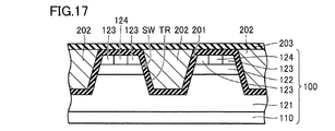
図17に示すように、ゲート電極202の露出面を覆うようにゲート電極202およびゲート酸化膜201上に層間絶縁膜203が形成される。
再び図7を参照して、層間絶縁膜203およびゲート酸化膜201に開口部が形成されるようにエッチングが行われる。この開口部により、メサ構造の上面においてn領域123およびコンタクト領域124の各々が露出される。次に、メサ構造の上面においてn領域123およびコンタクト領域124の各々に接するソース電極221が形成される。以上により半導体基板400が得られる。
なお半導体装置はMOSFET以外のMISFET(Metal Insulator Semiconductor Field Effect Transistor)であってもよい。また半導体装置は、MISFETに限定されるものではなく、たとえばIGBT(Insulated Gate Bipolar Transistor)であってもよい。また半導体装置は、トランジスタに限定されるものではなく、たとえばダイオードであってもよい。また半導体装置は、トレンチ型に限定されるものではなく、たとえばプレーナ型であってもよい。また半導体装置は、縦型に限定されるものではなく、たとえば横型であってもよい。
今回開示された実施の形態はすべての点で例示であって制限的なものではないと考えられるべきである。本発明の範囲は上記した説明ではなくて請求の範囲によって示され、請求の範囲と均等の意味および範囲内でのすべての変更が含まれることが意図される。
50 成膜部、60 測定部、61 膜厚測定部、70 制御部、222 ソース配線(導電体膜)、400 半導体基板、400D ダミー、500 MOSFET(半導体装置)。
Claims (6)
- 表面を有する半導体基板を準備する工程と、
前記半導体基板の前記表面を含む領域上に導電体膜を成膜する工程とを備え、
前記導電体膜を成膜する工程は、前記導電体膜が部分的に形成された時点で、部分的に形成された前記導電体膜の、交流損失および交流電気伝導率の少なくともいずれかに関する特性を測定する工程と、前記特性に基づいて、前記導電体膜を成膜するための成膜条件を調整する工程とを含む、半導体装置の製造方法。 - 前記特性を測定する工程は、部分的に形成された前記導電体膜に1×10⁶Hz以上1×10¹⁵Hz以下の周波数を有する交流電流を印加する工程を含む、請求項1に記載の半導体装置の製造方法。
- 前記導電体膜はワイヤボンディングのボンディングパッドとして構成された部分を含む、請求項1または2に記載の半導体装置の製造方法。
- 前記導電体膜を成膜する工程は、アルミニウム膜を成膜することによって行われる、請求項1~3のいずれか1項に記載の半導体装置の製造方法。
- 前記特性を測定する工程は、部分的に形成された前記導電体膜に第1の周波数を有する交流電流を印加する工程と、部分的に形成された前記導電体膜に第1の周波数と異なる第2の周波数を有する交流電流を印加する工程とを含む、請求項1~4のいずれか1項に記載の半導体装置の製造方法。
- 半導体基板の表面を含む領域上に導電体膜を成膜するための成膜部と、
前記領域上において、交流損失および交流電気伝導率の少なくともいずれかに関する特性を測定しかつ、導電体膜の厚さを測定するための測定部と、
前記特性に基づいて前記成膜部の成膜条件を調整するための制御部とを備える、成膜装置。
Applications Claiming Priority (2)
| Application Number | Priority Date | Filing Date | Title |
|---|---|---|---|
| JP2012139349A JP2014003250A (ja) | 2012-06-21 | 2012-06-21 | 半導体装置の製造方法および成膜装置 |
| JP2012-139349 | 2012-06-21 |
Publications (1)
| Publication Number | Publication Date |
|---|---|
| WO2013190895A1 true WO2013190895A1 (ja) | 2013-12-27 |
Family
ID=49768502
Family Applications (1)
| Application Number | Title | Priority Date | Filing Date |
|---|---|---|---|
| PCT/JP2013/061599 Ceased WO2013190895A1 (ja) | 2012-06-21 | 2013-04-19 | 半導体装置の製造方法および成膜装置 |
Country Status (3)
| Country | Link |
|---|---|
| US (1) | US20130344626A1 (ja) |
| JP (1) | JP2014003250A (ja) |
| WO (1) | WO2013190895A1 (ja) |
Citations (3)
| Publication number | Priority date | Publication date | Assignee | Title |
|---|---|---|---|---|
| WO2010073935A1 (ja) * | 2008-12-26 | 2010-07-01 | 東京エレクトロン株式会社 | 金属膜の膜厚測定方法及び基板処理方法及び装置 |
| JP2010236040A (ja) * | 2009-03-31 | 2010-10-21 | Asahi Kasei Electronics Co Ltd | 成膜装置 |
| JP2012158808A (ja) * | 2011-02-01 | 2012-08-23 | Asahi Glass Co Ltd | 成膜装置および成膜方法 |
Family Cites Families (10)
| Publication number | Priority date | Publication date | Assignee | Title |
|---|---|---|---|---|
| US5508610A (en) * | 1992-12-03 | 1996-04-16 | Georgia Tech Research Corporation | Electrical conductivity tester and methods thereof for accurately measuring time-varying and steady state conductivity using phase shift detection |
| US5445705A (en) * | 1994-06-30 | 1995-08-29 | International Business Machines Corporation | Method and apparatus for contactless real-time in-situ monitoring of a chemical etching process |
| US5559428A (en) * | 1995-04-10 | 1996-09-24 | International Business Machines Corporation | In-situ monitoring of the change in thickness of films |
| US6143155A (en) * | 1998-06-11 | 2000-11-07 | Speedfam Ipec Corp. | Method for simultaneous non-contact electrochemical plating and planarizing of semiconductor wafers using a bipiolar electrode assembly |
| JP3556549B2 (ja) * | 1999-12-10 | 2004-08-18 | シャープ株式会社 | シート抵抗測定器および電子部品製造方法 |
| JP2001217501A (ja) * | 2000-02-04 | 2001-08-10 | Sharp Corp | 半導体発光素子の電極形成方法および半導体発光素子 |
| US6515493B1 (en) * | 2000-04-12 | 2003-02-04 | Speedfam-Ipec Corporation | Method and apparatus for in-situ endpoint detection using electrical sensors |
| KR101526039B1 (ko) * | 2009-09-22 | 2015-06-04 | 아뎀, 엘엘씨 | 공진형 임피던스 센서, 임피던스 감지 시스템 및 물체의 화학적 및 물리적 특성을 측정하는 방법 |
| US9880233B2 (en) * | 2011-04-27 | 2018-01-30 | Applied Materials, Inc. | Methods and apparatus to determine parameters in metal-containing films |
| US9528814B2 (en) * | 2011-05-19 | 2016-12-27 | NeoVision, LLC | Apparatus and method of using impedance resonance sensor for thickness measurement |
-
2012
- 2012-06-21 JP JP2012139349A patent/JP2014003250A/ja active Pending
-
2013
- 2013-04-19 WO PCT/JP2013/061599 patent/WO2013190895A1/ja not_active Ceased
- 2013-05-14 US US13/894,106 patent/US20130344626A1/en not_active Abandoned
Patent Citations (3)
| Publication number | Priority date | Publication date | Assignee | Title |
|---|---|---|---|---|
| WO2010073935A1 (ja) * | 2008-12-26 | 2010-07-01 | 東京エレクトロン株式会社 | 金属膜の膜厚測定方法及び基板処理方法及び装置 |
| JP2010236040A (ja) * | 2009-03-31 | 2010-10-21 | Asahi Kasei Electronics Co Ltd | 成膜装置 |
| JP2012158808A (ja) * | 2011-02-01 | 2012-08-23 | Asahi Glass Co Ltd | 成膜装置および成膜方法 |
Also Published As
| Publication number | Publication date |
|---|---|
| JP2014003250A (ja) | 2014-01-09 |
| US20130344626A1 (en) | 2013-12-26 |
Similar Documents
| Publication | Publication Date | Title |
|---|---|---|
| JP6835192B2 (ja) | 炭化珪素半導体装置 | |
| CN103782391B (zh) | 碳化硅半导体器件及其制造方法 | |
| JP5526291B1 (ja) | 半導体装置及びその製造方法 | |
| CN112335057A (zh) | 碳化硅外延衬底及碳化硅半导体器件 | |
| WO2017056691A1 (ja) | 炭化珪素エピタキシャル基板の製造方法、炭化珪素半導体装置の製造方法および炭化珪素エピタキシャル基板の製造装置 | |
| JP5834801B2 (ja) | 半導体装置の製造方法および半導体装置 | |
| US20160218188A1 (en) | Silicon carbide semiconductor device and method for manufacturing the same | |
| CN103890952A (zh) | 碳化硅半导体器件及其制造方法 | |
| JP6226004B2 (ja) | 半導体装置および半導体装置の製造方法 | |
| JP2016213419A (ja) | 炭化珪素半導体装置 | |
| JP2023096663A (ja) | キャリア濃度の測定方法、炭化珪素エピタキシャル基板の製造方法および炭化珪素半導体装置の製造方法 | |
| CN106663631B (zh) | 碳化硅半导体装置及其制造方法 | |
| US8796123B2 (en) | Method of manufacturing silicon carbide semiconductor device | |
| WO2013190895A1 (ja) | 半導体装置の製造方法および成膜装置 | |
| WO2015049925A1 (ja) | 炭化珪素半導体装置およびその製造方法 | |
| WO2024058044A1 (ja) | 炭化珪素エピタキシャル基板、エピタキシャル基板の製造方法および炭化珪素半導体装置の製造方法 | |
| JP2014007325A (ja) | 炭化珪素半導体装置の製造方法 | |
| JP2016143788A (ja) | 炭化珪素半導体装置の製造方法 | |
| JP7505391B2 (ja) | 炭化珪素エピタキシャル基板の評価方法および炭化珪素半導体装置の製造方法 | |
| JP7661771B2 (ja) | 炭化珪素エピタキシャル基板の製造方法および炭化珪素半導体装置の製造方法 | |
| JP6070790B2 (ja) | 半導体装置の製造方法および半導体装置 | |
| JP2021005663A (ja) | 炭化珪素半導体装置および炭化珪素半導体装置の製造方法 | |
| US8866156B2 (en) | Silicon carbide semiconductor device and method for manufacturing same | |
| JP2025066386A (ja) | 炭化珪素基板の製造方法、炭化珪素エピタキシャル基板の製造方法、炭化珪素半導体装置の製造方法、および炭化珪素基板 | |
| WO2025062939A1 (ja) | 炭化珪素エピタキシャル基板、炭化珪素半導体装置および炭化珪素半導体装置の製造方法 |
Legal Events
| Date | Code | Title | Description |
|---|---|---|---|
| 121 | Ep: the epo has been informed by wipo that ep was designated in this application |
Ref document number: 13807460 Country of ref document: EP Kind code of ref document: A1 |
|
| NENP | Non-entry into the national phase |
Ref country code: DE |
|
| 122 | Ep: pct application non-entry in european phase |
Ref document number: 13807460 Country of ref document: EP Kind code of ref document: A1 |