WO2013183575A1 - Appareil d'antenne et appareil de communication sans fil - Google Patents
Appareil d'antenne et appareil de communication sans fil Download PDFInfo
- Publication number
- WO2013183575A1 WO2013183575A1 PCT/JP2013/065322 JP2013065322W WO2013183575A1 WO 2013183575 A1 WO2013183575 A1 WO 2013183575A1 JP 2013065322 W JP2013065322 W JP 2013065322W WO 2013183575 A1 WO2013183575 A1 WO 2013183575A1
- Authority
- WO
- WIPO (PCT)
- Prior art keywords
- coil conductor
- coil
- antenna device
- conductor
- antenna
- Prior art date
Links
Images


Classifications
-
- H—ELECTRICITY
- H01—ELECTRIC ELEMENTS
- H01Q—ANTENNAS, i.e. RADIO AERIALS
- H01Q7/00—Loop antennas with a substantially uniform current distribution around the loop and having a directional radiation pattern in a plane perpendicular to the plane of the loop
- H01Q7/06—Loop antennas with a substantially uniform current distribution around the loop and having a directional radiation pattern in a plane perpendicular to the plane of the loop with core of ferromagnetic material
-
- G—PHYSICS
- G06—COMPUTING; CALCULATING OR COUNTING
- G06K—GRAPHICAL DATA READING; PRESENTATION OF DATA; RECORD CARRIERS; HANDLING RECORD CARRIERS
- G06K19/00—Record carriers for use with machines and with at least a part designed to carry digital markings
- G06K19/06—Record carriers for use with machines and with at least a part designed to carry digital markings characterised by the kind of the digital marking, e.g. shape, nature, code
- G06K19/067—Record carriers with conductive marks, printed circuits or semiconductor circuit elements, e.g. credit or identity cards also with resonating or responding marks without active components
- G06K19/07—Record carriers with conductive marks, printed circuits or semiconductor circuit elements, e.g. credit or identity cards also with resonating or responding marks without active components with integrated circuit chips
- G06K19/077—Constructional details, e.g. mounting of circuits in the carrier
- G06K19/07749—Constructional details, e.g. mounting of circuits in the carrier the record carrier being capable of non-contact communication, e.g. constructional details of the antenna of a non-contact smart card
- G06K19/07773—Antenna details
- G06K19/07775—Antenna details the antenna being on-chip
-
- G—PHYSICS
- G06—COMPUTING; CALCULATING OR COUNTING
- G06K—GRAPHICAL DATA READING; PRESENTATION OF DATA; RECORD CARRIERS; HANDLING RECORD CARRIERS
- G06K19/00—Record carriers for use with machines and with at least a part designed to carry digital markings
- G06K19/06—Record carriers for use with machines and with at least a part designed to carry digital markings characterised by the kind of the digital marking, e.g. shape, nature, code
- G06K19/067—Record carriers with conductive marks, printed circuits or semiconductor circuit elements, e.g. credit or identity cards also with resonating or responding marks without active components
- G06K19/07—Record carriers with conductive marks, printed circuits or semiconductor circuit elements, e.g. credit or identity cards also with resonating or responding marks without active components with integrated circuit chips
- G06K19/077—Constructional details, e.g. mounting of circuits in the carrier
- G06K19/07749—Constructional details, e.g. mounting of circuits in the carrier the record carrier being capable of non-contact communication, e.g. constructional details of the antenna of a non-contact smart card
- G06K19/07773—Antenna details
- G06K19/07794—Antenna details the record carrier comprising a booster or auxiliary antenna in addition to the antenna connected directly to the integrated circuit
-
- H—ELECTRICITY
- H01—ELECTRIC ELEMENTS
- H01Q—ANTENNAS, i.e. RADIO AERIALS
- H01Q1/00—Details of, or arrangements associated with, antennas
- H01Q1/36—Structural form of radiating elements, e.g. cone, spiral, umbrella; Particular materials used therewith
- H01Q1/38—Structural form of radiating elements, e.g. cone, spiral, umbrella; Particular materials used therewith formed by a conductive layer on an insulating support
Definitions
- the present invention relates to an antenna device and a wireless communication device used in an RFID (Radio Frequency Identification) system and a near field communication (NFC) system.
- RFID Radio Frequency Identification
- NFC near field communication
- RFID system is widely used as a billing / fee collection management system.
- a reader / writer and an RFID tag are wirelessly communicated in a non-contact manner, and communication is performed between these devices.
- the reader / writer and the RFID tag each include an RFID IC chip for processing signals and an antenna for transmitting and receiving radio signals.
- signals are transmitted and received between the coil antenna on the reader / writer side and the coil antenna on the tag side via an induction magnetic field.
- Patent Documents 1 to 3 are known as antennas that can be used in such an HF band RFID system.
- JP 2004-166175 A Japanese Patent No. 3933191 JP 2009-284476 A
- an HF band RFID system is introduced into an information communication terminal such as a mobile phone, and the terminal itself may be used as a reader / writer or an RFID tag.
- a metal body such as a ground electrode of a printed wiring board or a battery pack may be located near the coil antenna.
- an eddy current that acts to cancel the magnetic field change of the coil antenna is generated, so that it is difficult to ensure a sufficient communication distance. Therefore, a coil antenna that can operate even when a metal body is in the vicinity is required.
- an antenna having a structure in which a magnetic material such as ferrite is sandwiched between a coil antenna and an object to be attached is known, as described in Patent Document 1.
- Patent Document 1 an antenna having a structure in which a magnetic material such as ferrite is sandwiched between a coil antenna and an object to be attached.
- Patent Document 2 discloses an antenna having a rectangular magnetic core, a first coil provided at one end thereof, and a second coil provided at the other end thereof.
- the first coil and the second coil have different coil winding directions, and the magnetic field that has entered between the coils can be guided in the direction of each coil. It is possible.
- this antenna although the communication distance in the top surface direction and the end portion direction of the magnetic core is large, it is difficult to ensure a large communication distance in the direction perpendicular to the axis of the magnetic core. That is, a direction with a low gain exists.
- Patent Document 3 discloses an antenna including a magnetic core whose end portions extend radially. Coils are wound around the radially extending magnetic core so as to have the same polarity. Since this antenna has directivity in the direction in which the magnetic core extends, the communication distance in these directions can be increased. However, in the antenna having this configuration, the shape of the magnetic core is complicated, and winding of the coil around the magnetic core is not easy.
- the present invention regards the above-mentioned problem as a problem to be solved, and has a simple structure, wide directivity, and less likely to cause eddy current loss in a nearby metal object, and a radio communication apparatus including the antenna device The purpose is to provide.
- the antenna device of the present invention includes a coil conductor wound in a coil shape, and the coil conductor includes a first coil conductor and a second coil conductor, and the first coil conductor and the coil conductor The coil opening of the second coil conductor is opposed to the magnetic material layer, and the first coil and the second coil are connected so that the directions of magnetic fluxes generated in the coil winding axis direction are opposite to each other. It is characterized by being.
- the magnetic flux entering from the coil opening of the first coil conductor can easily escape to the side (surface direction) from the gap between the first coil conductor and the second coil conductor. Therefore, it is possible to realize an antenna device that has a wide directivity and is less likely to cause eddy current loss in nearby metal objects.
- the said 1st coil conductor and the said 2nd coil conductor are connected in series as needed.
- the connection structure between the first coil conductor and the second coil conductor is simplified, and it is possible to connect to an external circuit through a two-pole signal line.
- the said 1st coil conductor and the said 2nd coil conductor are connected in parallel as needed. With this configuration, it is possible to easily reduce the impedance, and it is possible to connect to an external circuit with a two-pole signal line.
- the first coil conductor and the second coil conductor are coil conductors formed on a plane. With this configuration, the first coil conductor and the second coil conductor can be easily formed, and the entire antenna device can be thinned.
- the first coil conductor and the second coil conductor have substantially the same pattern when viewed in the coil winding axis direction.
- the symmetry between the magnetic field generated by the first coil conductor and the magnetic field generated by the second coil conductor is increased, and the magnetic flux that escapes to the side (plane direction) from the gap between the first coil conductor and the second coil conductor is coiled. It is along the surface direction of the opening surface.
- a metal object may be disposed on the opposite side of the coil opening surface of the second coil conductor from the side on which the first coil conductor is provided.
- the first coil conductor and the second coil conductor facing each other through the magnetic layer act as a feeding coil for the booster antenna, and the booster antenna and the feeding coil can be arranged in a disconnected state.
- the magnetic layer is a magnetic layer of a multilayer substrate including a magnetic layer, and the first coil conductor and the second coil conductor are formed on the magnetic layer or the non-magnetic layer of the multilayer substrate. Preferably it is. With this configuration, each member is integrated and can be handled as a thin single component, and for example, surface mounting on a substrate is facilitated.
- a wireless communication device of the present invention includes a communication circuit and an antenna device connected to the communication circuit, and the antenna device includes a coil conductor wound in a coil shape, and the coil conductor Is composed of a first coil conductor and a second coil conductor, and the first coil conductor and the second coil conductor are arranged such that coil openings are opposed to each other across a magnetic layer, and the first coil conductor and the second coil conductor The second coil conductors are connected so that the directions of magnetic fluxes generated in the coil winding axis direction are opposite to each other.
- the magnetic flux since the magnetic flux enters and exits the gap between the first coil conductor and the second coil conductor, the magnetic flux enters and exits in the 360 ° direction, and wide directivity is obtained.
- magnetic flux that enters the coil openings of the first and second coil conductors from the vertical direction passes through the gap between the first coil conductor and the second coil conductor to the side (surface direction), so eddy current loss occurs in nearby metal objects. Is less likely to occur, and low loss characteristics can be obtained.
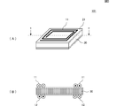
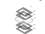
- FIG. 1 is an exploded perspective view of an antenna device 101 according to the first embodiment.
- FIG. 2A is a diagram showing a connection relationship between the first coil conductor 11 and the second coil conductor 12.
- FIG. 2B is an equivalent circuit diagram of the circuit shown in FIG. 3A is a perspective view of the antenna device 101, and FIG. 3B is a cross-sectional view of the xx portion in FIG. 3A.
- FIG. 4A is a perspective view illustrating a path through which magnetic flux passes in a state where the metal body 40 is disposed in the vicinity of the antenna device 101.
- FIG. 4B is a cross-sectional view of FIG.
- FIG. 5 is a diagram showing a connection structure between the first coil conductor 11 and the second coil conductor 12 for the antenna device 102 of the second embodiment.
- FIG. 6A is an exploded perspective view of the antenna device 103 according to the third embodiment
- FIG. 6B is a cross-sectional view of the antenna device 103
- FIG. 7A is an exploded perspective view showing the relationship between the sizes of the first coil conductor 11 and the second coil conductor 12 in the antenna device of the fourth embodiment.
- FIG. 7B is a cross-sectional view showing a path through which the magnetic flux passes in a state where the metal body 40 is disposed in the vicinity of the antenna device shown in FIG.
- FIG. 8A is an exploded perspective view showing the size relationship between the first coil conductor 11 and the second coil conductor 12 in relation to another antenna device according to the fourth embodiment.
- FIG. 7A is an exploded perspective view showing the relationship between the sizes of the first coil conductor 11 and the second coil conductor 12 in relation to another antenna device according to the fourth embodiment.
- FIG. 8B is a cross-sectional view illustrating a path through which the magnetic flux passes in a state where the metal body 40 is disposed in the vicinity of the antenna device illustrated in FIG.
- FIG. 9A is an exploded perspective view showing a difference in the number of turns between the first coil conductor 11 and the second coil conductor 12 in another antenna device of the fifth embodiment.
- FIG. 9B is a cross-sectional view showing a path through which the magnetic flux passes in a state where the metal body 40 is disposed in the vicinity of the antenna device shown in FIG.
- FIG. 10A is an exploded perspective view showing the difference in the number of turns between the first coil conductor 11 and the second coil conductor 12 in another antenna device of the fifth embodiment.
- FIG. 10B is a cross-sectional view illustrating a path through which the magnetic flux passes in a state where the metal body 40 is disposed in the vicinity of the antenna device illustrated in FIG.
- FIG. 11A is an exploded perspective view of the antenna device 106 according to the sixth embodiment.
- FIG. 11B is an equivalent circuit diagram of the antenna device 106.
- FIG. 12 is a cross-sectional view of a main part of a wireless communication apparatus according to the seventh embodiment.
- FIG. 13A is a perspective view showing the positional relationship between the substrate 60, the antenna device 103, and the resonance booster 201.
- FIG. 13B is a plan view seen from the resonance booster with the casing removed.
- FIG. 14 is an exploded perspective view of the resonance booster 201.
- FIG. 15 is an equivalent circuit diagram in a state where the feeding circuit 9 is connected to the antenna device 103.
- FIG. 16 is a diagram showing how the antenna device 103 and the resonant booster 201 are coupled.
- FIG. 17 is a cross-sectional view of a main part of a wireless communication apparatus according to the eighth embodiment.
- FIG. 18A is a perspective view showing a positional relationship among the substrate 60, the feeding antenna 202, and the antenna device 108.
- FIG. 18B is a plan view seen from the antenna device 108 with the housing removed.
- FIG. 19A is an exploded perspective view of the antenna device 108, and FIG. 19B is an equivalent circuit diagram of the antenna device 108.
- FIG. 20 is a diagram illustrating a state of coupling between the feeding antenna 202 and the antenna device 108.
- FIG. 21 is a cross-sectional view of a main part of a wireless communication apparatus according to the ninth embodiment.
- 22A is a perspective view of an antenna device as a comparative example of the antenna device 101
- FIG. 22B is a cross-sectional view taken along the line xx in FIG. 22A.
- FIG. 23A is a perspective view showing a path through which magnetic flux passes in the state where the metal body 40 is disposed in the vicinity of the antenna device as the comparative example shown in FIG.
- FIG. 23B is a cross-sectional view thereof.
- FIG. 24 is an exploded perspective view of the antenna device 110 according to the tenth embodiment.
- FIG. 25A is a plan view in a state where the antenna device 110 is disposed in the vicinity of the planar metal body 40.
- FIG. 25B is a plan view showing another arrangement state of the metal body 40 and the antenna device 110.
- FIG. 26 is a cross-sectional view showing a path through which the magnetic flux passes in a state where the planar metal body 40 is disposed in the vicinity of the antenna device 110.
- FIG. 27 is an exploded perspective view of the antenna device 111 according to the eleventh embodiment.
- FIG. 28 is a cross-sectional view showing a path through which the magnetic flux passes in a state where the planar metal body 40 is disposed in the vicinity of the antenna device 111.
- FIG. 29 is a cross-sectional view of a main part of a wireless communication apparatus according to the twelfth embodiment.
- FIG. 1 is an exploded perspective view of an antenna device 101 according to the first embodiment.
- the antenna device 101 is an antenna device used in an HF band communication system, and includes a first coil conductor 11, a second coil conductor 12, and a magnetic layer 30.
- the 1st coil conductor 11 is formed in the upper surface of the base material 21 which is a nonmagnetic material sheet.
- the 2nd coil conductor 12 is formed in the lower surface of the base material 22 which is a nonmagnetic material sheet.
- first coil conductor 11 and the second coil conductor 12 are formed by patterning a metal film such as a Cu foil provided on flexible base materials 21 and 22 made of polyethylene terephthalate or the like into a coil shape. Is done.
- the opposing surfaces of the first coil conductor 11 and the second coil conductor 12 are preferably substantially parallel to each other.
- the magnetic layer 30 may be a ferrite sintered body (ferrite ceramic) formed by molding and firing ferrite powder, or a magnetic body powder such as ferrite is dispersed in a resin such as an epoxy resin.
- the composite magnetic body may be formed into a sheet shape.
- the shape of the magnetic layer 30 is rectangular (rectangular plate) in the present embodiment, but may be other shapes such as circular (disc).
- the first coil conductor 11 and the second coil conductor 12 are arranged so that the respective coil openings are opposed to each other through the magnetic layer 30.
- the inner peripheral end of the first coil conductor 11 and the inner peripheral end of the second coil conductor 12 are electrically connected.
- FIG. 2A is a diagram showing a connection relationship between the first coil conductor 11 and the second coil conductor 12. As shown in FIG. 2A, the first coil conductor 11 and the second coil conductor 12 are connected so that the directions of magnetic fluxes generated in the coil winding axis direction are opposite to each other.
- FIG. 2B is an equivalent circuit diagram of the circuit shown in FIG.
- the inductor L11 corresponds to the first coil conductor 11
- the inductor L12 corresponds to the second coil conductor 12. That is, in this example, the first coil conductor 11 and the second coil conductor 12 are connected in series and connected to the power feeding circuit 9.
- FIG. 3A is a perspective view of the antenna device 101
- FIG. 3B is a cross-sectional view of the xx portion in FIG. 3A.
- the first coil conductor 11 and the second coil conductor 12 have a circular cross-section and are exaggerated and drawn to represent the direction of current.
- the direction of the current flowing through the first coil conductor 11 and the second coil conductor 12 at this timing coincides with the direction indicated by the arrow in FIG.
- FIG. 22A is a perspective view of an antenna device as a comparative example of the antenna device 101
- FIG. 22B is a cross-sectional view of the xx portion in FIG. 22A (coil winding axes of the coil conductors 18 and 19).
- the direction of the current flowing through the coil conductors 11 and 12 is the same as the direction of the current flowing through the coil conductors 18 and 19 in these cross sections.
- FIG. 4A is a perspective view showing a path through which the magnetic flux passes in a state where the planar metal body 40 is disposed in the vicinity of the antenna device 101.
- FIG. 4B is a cross-sectional view thereof.
- the metal body 40 may be a ground of a printed wiring board disposed in a housing of the communication terminal, for example, or may be a metal body such as a battery pack or a shield case. Moreover, a part of metal housing may be sufficient.
- FIG. 23A is a perspective view showing a path through which the magnetic flux passes in the state where the metal body 40 is disposed in the vicinity of the antenna device as the comparative example shown in FIG.
- FIG. 23B is a cross-sectional view thereof.
- the magnetic flux ⁇ incident on the metal body 40 in the vertical direction is the side (surface) of the magnetic layer 30. Direction).
- the magnetic flux incident perpendicularly to the metal surface follows the metal surface. Exit in the direction.
- the magnetic flux that enters from the coil opening of the first coil conductor 11 of the antenna device 101 passes from the gap between the first coil conductor 11 and the second coil conductor 12 to the side (surface direction), so that the magnetic flux passes through the first coil. Interlinks with the conductor 11.
- the antenna device 101 of the present invention differs from the antenna device as a comparative example shown in FIGS. 22A and 23A in that the magnetic flux incident perpendicularly to the metal surface is 360 ° along the metal surface. Magnetic flux escapes in the direction. Therefore, an antenna device having a wide directivity and less likely to cause eddy current loss in a nearby metal object can be realized, and is particularly useful as an antenna device arranged on a metal surface.
- the connection structure between the first coil conductor 11 and the second coil conductor 12 is simplified.
- it can be connected to an external circuit with a two-pole signal line.
- first coil conductor 11 and the second coil conductor 12 are formed on a plane, the first coil conductor 11 and the second coil conductor 12 can be easily formed, and the entire antenna device can be thinned.
- first coil conductor 11 and the second coil conductor 12 have substantially the same pattern when viewed in the coil winding axis direction, the magnetic field generated by the first coil conductor 11 and the magnetic field generated by the second coil conductor 12 are different.
- the symmetry increases, and the magnetic flux that escapes to the side (surface direction) from the gap between the first coil conductor 11 and the second coil conductor 12 is along the surface direction of the coil opening surface.
- FIG. 5 is a diagram showing a connection structure between the first coil conductor 11 and the second coil conductor 12 for the antenna device 102 of the second embodiment.
- the arrow in FIG. 5 represents the direction of current.
- the first coil conductor 11 and the second coil conductor 12 are connected in series.
- the antenna device 102 according to the second embodiment includes the first coil conductor 11 and the second coil conductor 12. Electrically connected in parallel and connected to the power supply circuit 9.
- the first coil conductor 11 and the second coil conductor 12 are connected so that the directions of magnetic fluxes generated in the coil winding axis directions are opposite to each other. .
- first coil conductor 11 and the second coil conductor 12 may be connected in parallel as necessary. With this configuration, the impedance can be easily reduced.
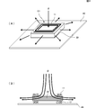
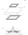
- FIG. 6A is an exploded perspective view of the antenna device 103 according to the third embodiment
- FIG. 6B is a cross-sectional view of the antenna device 103.
- the antenna device 103 includes a first coil conductor 11, a second coil conductor 12, and a magnetic layer 30.
- the first coil conductor 11 is formed on the upper surface of the magnetic layer 30.
- the second coil conductor 12 is formed on the upper surface of the nonmagnetic layer 32.
- Input / output terminals 51 and 52 and vacant terminals 53 and 54 for mounting are formed on the lower surface of the nonmagnetic layer 32.
- the nonmagnetic layers 31 and 32 are, for example, dielectric ceramics, and the magnetic layer 30 is magnetic ceramics. As shown in FIG. 6B, the non-magnetic layers 31 and 32 and the magnetic layer 30 are laminated in a green sheet state and integrally fired.
- first coil conductor 11 and the second coil conductor 12 may be integrated together with the magnetic layer.
- each member is integrated and can be handled as a thin single component, and for example, surface mounting on a substrate is facilitated.
- FIG. 7A is an exploded perspective view showing the relationship between the sizes of the first coil conductor 11 and the second coil conductor 12 in the antenna device of the fourth embodiment.
- FIG. 7B is a cross-sectional view showing a path through which the magnetic flux passes in a state where the metal body 40 is disposed in the vicinity of the antenna device.
- the coil winding axes of the first coil conductor 11 and the second coil conductor 12 are the same, but the winding range of the second coil conductor 12 is smaller than the winding range of the first coil conductor 11.
- FIG. 8A is an exploded perspective view showing the size relationship between the first coil conductor 11 and the second coil conductor 12 for another antenna device of the fourth embodiment.
- FIG. 8B is a cross-sectional view showing a path through which the magnetic flux passes in a state where the metal body 40 is disposed in the vicinity of the antenna device.
- the coil winding axes of the first coil conductor 11 and the second coil conductor 12 coincide with each other, but the winding range of the first coil conductor 11 is smaller than the winding range of the second coil conductor 12.
- the magnetic flux ⁇ escapes on the side of the magnetic layer 30 and away from the metal body 40. Therefore, even if the metal body 40 is disposed in close proximity to the antenna device, the eddy current can be prevented from flowing through the metal body 40.
- a metal object such as a battery pack having a thickness larger than that of the antenna device is disposed on the side of the antenna device, it is possible to suppress an eddy current from flowing through the metal object.
- FIG. 9A is an exploded perspective view showing a difference in the number of turns between the first coil conductor 11 and the second coil conductor 12 in another antenna device of the fifth embodiment.
- FIG. 9B is a cross-sectional view showing a path through which the magnetic flux passes in a state where the metal body 40 is disposed in the vicinity of the antenna device.
- the coil winding axes of the first coil conductor 11 and the second coil conductor 12 are the same, but the number of turns of the first coil conductor 11 is greater than the number of turns of the second coil conductor 12.
- the number of turns of the first coil conductor 11 and the second coil conductor 12 may be different.
- FIG. 10A is an exploded perspective view showing the difference in the number of turns between the first coil conductor 11 and the second coil conductor 12 in relation to another antenna device of the fifth embodiment.
- FIG. 10B is a cross-sectional view showing a path through which the magnetic flux passes in a state where the metal body 40 is disposed in the vicinity of the antenna device.
- the coil winding axes of the first coil conductor 11 and the second coil conductor 12 are the same, but the winding range of the second coil conductor 12 is larger than the winding range of the first coil conductor 11.
- the coil opening of the second coil conductor 12 is small, the magnetic flux that tends to escape from the surface on which the second coil conductor 12 is formed is reduced. Even if they are arranged in close proximity, the eddy current can be prevented from flowing through the metal body 40.
- a metal object such as a battery pack having a thickness larger than that of the antenna device is disposed on the side of the antenna device, it is possible to suppress an eddy current from flowing through the metal object.
- FIG. 11A is an exploded perspective view of the antenna device 106 according to the sixth embodiment.
- the antenna device 106 includes a first coil conductor 11, a second coil conductor 12, and a magnetic layer 30.
- the 1st coil conductor 11 is formed in the upper surface of the base material 21 which is a nonmagnetic material sheet.
- the 2nd coil conductor 12 is formed in the lower surface of the base material 22 which is a nonmagnetic material sheet.
- a capacitor forming electrode 13 is formed on the base material 21, and the capacitor forming electrode 13 is connected to the inner peripheral end of the first coil conductor 11.
- a capacitance forming electrode 14 is formed on the base material 22, and the capacitance forming electrode 14 is connected to the inner peripheral end of the second coil conductor 12.
- the capacitance forming electrodes 13 and 14 are arranged to face each other with the base materials 21 and 22 and the magnetic layer 30 interposed therebetween.
- FIG. 11B is an equivalent circuit diagram of the antenna device 106.
- the inductor L11 corresponds to the first coil conductor 11
- the inductor L12 corresponds to the second coil conductor 12
- the capacitor C12 corresponds to the capacitance generated between the capacitance forming electrodes 13-14. According to this structure, the wiring which directly connects between the 1st coil conductor 11 and the 2nd coil conductor 12 becomes unnecessary, and manufacture becomes easy.
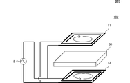
- FIG. 12 is a cross-sectional view of a main part of a wireless communication apparatus according to the seventh embodiment.
- This wireless communication device is, for example, a mobile phone terminal.
- a substrate 60 is housed inside the housing 90.
- the antenna device 103 is mounted on the upper surface (the lower surface in the actual use state) of the substrate 60 in the drawing.
- a resonance booster 201 is attached to the inner surface of the housing 90.
- the antenna device 103 is the one shown in FIG. 6 in the third embodiment.
- the substrate 60 is composed of a base material 69 and various electrodes formed on the base material 69.
- the input / output terminals 51 and 52 of the antenna device 103 are soldered to the mounting pad electrodes 61 and 62 on the substrate.
- a ground conductor 68 is formed on almost the entire surface of the substrate 60.
- FIG. 13A is a perspective view showing the positional relationship between the substrate 60, the antenna device 103, and the resonance booster 201.
- FIG. 13B is a plan view seen from the resonance booster 201 side with the casing removed.
- FIG. 14 is an exploded perspective view of the resonance booster 201.
- the resonance booster 201 includes a base sheet 70 such as PET, a coil conductor 71 formed on the top surface of the base sheet 70, and a coil conductor 72 formed on the bottom surface.
- the coil conductor 71 and the coil conductor 72 are planar coils.
- the coil conductor 71 and the coil conductor 72 are wound patterns so that the current flows in each coil conductor in the same direction when a current flows from one end to the other end of each coil conductor.
- the coil conductors 71 and 72 are arranged so that at least a part of the coil conductors 71 and 72 overlap when viewed in plan from the winding axis direction. Couple through capacity.
- FIG. 15 is an equivalent circuit diagram in a state where the feeding circuit 9 is connected to the antenna device 103.
- an LC resonance circuit including a stray capacitance and a matching capacitor included in the RFID IC chip itself and inductances L11 and L12 by coil conductors is configured.
- the resonance frequency of this LC resonance circuit is set to be approximately equal to the carrier frequency (13.56 MHz) of the communication signal.
- the resonance booster 201 includes an LC resonance circuit including an inductance L71 of the coil conductor 71, an inductance L72 of the coil conductor 72, and capacitors C12 and C21 formed between the coil conductor 71 and the coil conductor 72. .
- the resonance frequency of this LC resonance circuit is set to be close to the carrier frequency (13.56 MHz) of the communication signal.
- the antenna device 103 and the resonant booster 201 are magnetically coupled to each other.
- FIG. 16 is a diagram showing a state of coupling between the antenna device 103 and the resonance booster 201.
- the communication partner antenna and the resonance booster 201 are magnetically coupled to each other by the magnetic flux ⁇ 1 incident on the substrate 60 in the vertical direction by the communication partner antenna being linked to the coil conductors 71 and 72 of the resonance booster 201. Further, the magnetic flux ⁇ 2 generated by the current flowing through the coil conductors 71 and 72 of the resonance booster 201 is linked to the first coil conductor 11 of the antenna device 103, so that the resonance booster 201 and the antenna device 103 are magnetically coupled.
- the antenna by the resonance booster 201 and the antenna device 103 is an example of acting as a reception antenna. However, due to the reversibility of the antenna, the antenna is also similarly coupled when acting as a transmission antenna.
- the resonance booster 201 Since the coil opening of the coil conductors 71 and 72 of the resonance booster 201 is larger than the coil opening of the first coil conductor 11 of the antenna device 103, the resonance booster 201 is strongly coupled to the communication partner antenna, and the resonance booster 201 and the antenna device 103 Overall gain increases.
- FIG. 17 is a cross-sectional view of a main part of a wireless communication apparatus according to the eighth embodiment.
- This wireless communication device is, for example, a mobile phone terminal.
- a substrate 60 is housed inside the housing 90.
- a feeding antenna 202 is mounted on the upper surface (the lower surface in the actual use state) of the substrate 60 in the drawing.
- An antenna device 108 as a resonance booster is attached to the inner surface of the housing 90.
- the input / output terminals of the power feeding antenna 202 are soldered to the mounting pad electrodes on the substrate.
- a ground conductor 68 is formed on almost the entire surface of the substrate 60.
- FIG. 18A is a perspective view showing a positional relationship among the substrate 60, the feeding antenna 202, and the antenna device 108.
- FIG. FIG. 18B is a plan view seen from the antenna device 108 with the housing removed.
- FIG. 19A is an exploded perspective view of the antenna device 108, and
- FIG. 19B is an equivalent circuit diagram of the antenna device 108.
- the antenna device 108 as a resonance booster includes a first coil conductor 11, a second coil conductor 12, and a magnetic layer 30, and the first coil conductor 11 and the second coil conductor 11.
- the coil opening of the coil conductor 12 is opposed to the coil conductor 12 via the magnetic layer 30.
- the inner end of the first coil conductor 11 and the inner end of the second coil conductor 12 are electrically connected, and the outer peripheral ends of the first coil conductor 11 and the second coil conductor 12 are open.
- a capacitance is generated between the first coil conductor 11 and the second coil conductor 12.
- the inductor L11 corresponds to the first coil conductor 11
- the inductor L12 corresponds to the second coil conductor 12
- the capacitor C is generated between the first coil conductor 11 and the second coil conductor 12.
- the resonance frequency of the LC resonance circuit including the inductors L11 and L12 and the capacitor C is set to be a frequency near the carrier frequency of the communication signal.
- the power supply antenna 202 includes a magnetic layer 80 and a coil conductor 83 having a shape wound around the magnetic layer 80.
- the feeding antenna 202 is mounted on the substrate 60 so that the coil winding axis of the coil conductor 83 is parallel to the surface of the substrate 60.
- FIG. 20 is a diagram showing a state of coupling between the feeding antenna 202 and the antenna device 108.
- the magnetic flux ⁇ 1 generated by the power feeding antenna is linked to the second coil conductor 12 of the antenna device 108 as a resonance booster, so that the power feeding antenna 202 and the antenna device 108 are magnetically coupled.
- the magnetic flux ⁇ 2 generated by the current flowing through the first coil conductor 11 of the antenna device 108 is linked to the communication partner antenna, so that the antenna device 108 and the communication partner antenna are magnetically coupled.
- the antenna device 108 Since the coil opening of the coil conductors 11 and 12 of the antenna device 108 as a resonance booster is larger than the coil opening of the coil conductor 83 of the power feeding antenna 202, the antenna device 108 is strongly coupled to the antenna of the communication partner, and the antenna device 108 and the power feeding antenna. The overall gain due to 202 is increased.
- the antenna by the antenna device 108 and the feeding antenna 202 acts as a transmitting antenna.
- the antenna device 108 and the feeding antenna 202 are similarly coupled when acting as a receiving antenna.
- FIG. 21 is a cross-sectional view of a main part of a wireless communication apparatus according to the ninth embodiment.
- the coil openings of the first coil conductor 11 and the second coil conductor 12 and the magnetic layer 30 may be curved surfaces.
- the antenna device 109 is disposed (attached) along the curved surface of the casing 90 of the wireless communication device.
- the antenna device 109 is connected to a circuit on the substrate 60 side via the pin terminal 67 in a state where the case to which the antenna device 109 is attached is covered.
- the basic configuration of the antenna device 109 is the same as that shown in the first embodiment.
- the first coil conductor 11 is formed on a flexible resin base material 21, and the second coil conductor 12 is formed on a flexible resin base material 22.
- the magnetic layer 30 is a flexible magnetic resin sheet in which a magnetic filler is dispersed.
- the first end of the first coil conductor 11 is connected to the first end of the second coil conductor 12 via an interlayer connection conductor provided in the magnetic layer 30.
- the second end of the first coil conductor 11 is drawn out to the surface of the base material 22 via an interlayer connection conductor provided on the magnetic layer 30.
- a second end of the second coil conductor 12 is connected to a power feeding circuit (RFIC chip) via a first pin terminal 67.
- the second end of the first coil conductor 11 is connected to a power supply circuit provided on the printed wiring board 60 via a second pin terminal.
- the directivity centering on the arrow direction in the figure is shown. Therefore, the directivity is particularly suitable for usage in which one side of the housing is brought into contact with the reading unit of the communication counterpart device.
- FIG. 24 is an exploded perspective view of the antenna device 110 according to the tenth embodiment.
- the first coil conductor 11 is formed on the upper surface of the magnetic layer 30, and the second coil conductor 12 is formed on the lower surface of the magnetic layer 30.
- the patterns of the first coil conductor 11 and the second coil conductor 12 are similar, the centers of the coil openings are shifted from each other in plan view.
- FIG. 25A is a plan view in a state where the antenna device 110 is disposed in the vicinity of the planar metal body 40.
- FIG. 26 is a cross-sectional view showing a path through which the magnetic flux passes in a state where the planar metal body 40 is disposed in the vicinity of the antenna device 110.
- the antenna device 11 When the coil conductor and the planar metal body 40 are viewed in plan, the antenna device 11 is arranged close to the end (edge) of the planar metal body 40 as shown in FIG.
- the coil opening centers of the two coil conductors 11 and 12 facing each other are shifted from each other in a plan view (the planar shape). 26.
- the end of the metal body 40 is as shown by the magnetic flux ⁇ a shown in FIG.
- the magnetic field can easily escape through the part.
- unnecessary coupling with the metal body 40 is suppressed as indicated by the magnetic flux ⁇ b.
- the electrode width and the interelectrode gap of the coil conductors 11 and 12 may be different from each other.
- the electrode width on the sides S2 and S4 in contact with the side S1 closest to the end of the planar metal body 40 in the coil conductor 11 is narrower than the electrode width on the sides S1 and S3. May be.
- the electrode pitch on the sides S2 and S4 may be narrower than the electrode pitch on the sides S1 and S3.
- the electrode width or electrode pitch may be determined as described above.
- FIG. 25B is a plan view showing another arrangement state of the metal body 40 and the antenna device 110. As shown in FIG. 25B, the side S1 closest to the end of the metal body 40 in the outer shape of the coil conductor 11 may be non-parallel to the side SN constituting the end of the metal body. .
- the length from the intersection p1 between the perpendicular line L1 and the end of the metal body 40 to the middle point c1 of the side S1. Is the distance between the side S1 and the end of the metal body 40.
- the length from the intersection point p2 between the perpendicular line L2 and the end of the metal body 40 to the middle point c2 of the side S2 Is the distance between the side S2 and the end of the metal body 40.
- the distance between all sides (sides S1 to S4) in the outer shape of the coil conductor 11 and the end of the metal body 40 is calculated, and the shortest side of this distance is “the end of the metal body 40 in the outer shape of the coil conductor 11”. The side closest to the part.
- the metal body 40 may be, for example, a ground of a printed wiring board arranged in a communication terminal housing, as in the embodiments shown so far, or may be a battery pack or a shield case. A conductive plate may be used. Moreover, a part of metal housing may be sufficient.
- FIG. 27 is an exploded perspective view of the antenna device 111 according to the eleventh embodiment.
- FIG. 28 is a cross-sectional view showing a path through which the magnetic flux passes in a state where the planar metal body 40 is disposed in the vicinity of the antenna device 111.
- first coil conductors 11A and 11B are formed on the upper surface of the magnetic layer 30, and second coil conductors 12A and 12B are formed on the lower surface of the magnetic layer 30, respectively.
- the first coil conductors 11A and 11B and the second coil conductors 12A and 12B may each have a laminated structure.
- the coil opening diameter can be increased in a small area while ensuring the necessary number of turns.
- both the first coil conductor and the second coil conductor have two layers, the number of coil layers may be further increased, or the first coil conductor and the second coil conductor may have different layers.
- FIG. 29 is a cross-sectional view of a main part of a wireless communication apparatus according to the twelfth embodiment.
- the antenna device 112 is arranged (attached) along the curved surface of the housing 90 of the wireless communication device.
- the antenna device 112 is connected to a circuit on the substrate 60 side via a pin terminal 67.
- the basic configuration of the antenna device 112 is the same as that shown in the first embodiment.
- the first coil conductor 11 is formed on a flexible resin base material 21, and the second coil conductor 12 is formed on a flexible resin base material 22.
- the antenna device 112 is arranged along a plurality of surfaces of the housing 90. With this configuration, the directivity can be expanded as indicated by the white arrow in FIG.
- a feeding coil may be mounted instead of the pin terminal 67. Even with this configuration, communication from the non-mounting surface side of the power feeding coil is possible.
Landscapes
- Engineering & Computer Science (AREA)
- Microelectronics & Electronic Packaging (AREA)
- Computer Networks & Wireless Communication (AREA)
- Computer Hardware Design (AREA)
- Physics & Mathematics (AREA)
- General Physics & Mathematics (AREA)
- Theoretical Computer Science (AREA)
- Support Of Aerials (AREA)
- Details Of Aerials (AREA)
Abstract
La présente invention porte sur un appareil d'antenne (101) qui comporte un premier conducteur de bobine (11), un second conducteur de bobine (12), et une couche de matériau magnétique (30). Le premier conducteur de bobine (11) et le second conducteur de bobine (12) ont des ouvertures de bobine respectives disposées en regard l'une de l'autre avec les couches de la couche de matériau magnétique (30) entre elles. L'extrémité circonférentielle intérieure du premier conducteur de bobine (11) et l'extrémité circonférentielle intérieure du second conducteur de bobine (12) sont connectées électriquement l'une à l'autre. Le premier conducteur de bobine (11) et le second conducteur de bobine (12) sont connectés l'un à l'autre de telle sorte que les directions des flux magnétiques générés dans la direction de l'axe de bobinage de bobine sont opposées l'une à l'autre. Un flux magnétique (φ) qui entre dans la direction perpendiculaire à un corps métallique (40) circule à l'opposé des côtés (dans la direction de surface) de la couche de matériau magnétique (30).
Priority Applications (2)
| Application Number | Priority Date | Filing Date | Title |
|---|---|---|---|
| JP2013552786A JP5757345B2 (ja) | 2012-06-04 | 2013-06-03 | 無線通信装置 |
| US14/200,128 US9583834B2 (en) | 2012-06-04 | 2014-03-07 | Antenna module and radio communication device |
Applications Claiming Priority (2)
| Application Number | Priority Date | Filing Date | Title |
|---|---|---|---|
| JP2012126653 | 2012-06-04 | ||
| JP2012-126653 | 2012-06-04 |
Related Child Applications (1)
| Application Number | Title | Priority Date | Filing Date |
|---|---|---|---|
| US14/200,128 Continuation US9583834B2 (en) | 2012-06-04 | 2014-03-07 | Antenna module and radio communication device |
Publications (1)
| Publication Number | Publication Date |
|---|---|
| WO2013183575A1 true WO2013183575A1 (fr) | 2013-12-12 |
Family
ID=49711967
Family Applications (1)
| Application Number | Title | Priority Date | Filing Date |
|---|---|---|---|
| PCT/JP2013/065322 WO2013183575A1 (fr) | 2012-06-04 | 2013-06-03 | Appareil d'antenne et appareil de communication sans fil |
Country Status (3)
| Country | Link |
|---|---|
| US (1) | US9583834B2 (fr) |
| JP (2) | JP5757345B2 (fr) |
| WO (1) | WO2013183575A1 (fr) |
Cited By (12)
| Publication number | Priority date | Publication date | Assignee | Title |
|---|---|---|---|---|
| CN104299025A (zh) * | 2014-09-22 | 2015-01-21 | 武汉天喻信息产业股份有限公司 | 具有防丢失功能的非接触智能卡及其工作方法 |
| CN104868251A (zh) * | 2014-02-20 | 2015-08-26 | 联想(北京)有限公司 | 一种nfc天线 |
| EP2942878A1 (fr) * | 2014-05-05 | 2015-11-11 | Nxp B.V. | Antenne de communication à travers le corps humain |
| CN106329077A (zh) * | 2016-09-26 | 2017-01-11 | 上海德门电子科技有限公司 | 基于双面板走线的nfc天线及电子设备 |
| CN106486778A (zh) * | 2015-08-26 | 2017-03-08 | 恩智浦有限公司 | 天线系统 |
| US9812788B2 (en) | 2014-11-24 | 2017-11-07 | Nxp B.V. | Electromagnetic field induction for inter-body and transverse body communication |
| US9819395B2 (en) | 2014-05-05 | 2017-11-14 | Nxp B.V. | Apparatus and method for wireless body communication |
| US10009069B2 (en) | 2014-05-05 | 2018-06-26 | Nxp B.V. | Wireless power delivery and data link |
| US10014578B2 (en) | 2014-05-05 | 2018-07-03 | Nxp B.V. | Body antenna system |
| US10015604B2 (en) | 2014-05-05 | 2018-07-03 | Nxp B.V. | Electromagnetic induction field communication |
| JP2018170679A (ja) * | 2017-03-30 | 2018-11-01 | 株式会社村田製作所 | アンテナ装置及び電子機器 |
| US10320086B2 (en) | 2016-05-04 | 2019-06-11 | Nxp B.V. | Near-field electromagnetic induction (NFEMI) antenna |
Families Citing this family (28)
| Publication number | Priority date | Publication date | Assignee | Title |
|---|---|---|---|---|
| WO2011118379A1 (fr) * | 2010-03-24 | 2011-09-29 | 株式会社村田製作所 | Système d'identification par radiofréquence |
| TWI604480B (zh) | 2012-03-23 | 2017-11-01 | Lg伊諾特股份有限公司 | 無線功率接收器以及包含有其之可攜式終端裝置 |
| JP6313744B2 (ja) | 2012-03-23 | 2018-04-18 | エルジー イノテック カンパニー リミテッド | 無線電力受信機 |
| USD749062S1 (en) * | 2013-01-02 | 2016-02-09 | Callas Enterprises Llc | Combined floor mat and EAS antenna |
| CN205080956U (zh) * | 2013-04-16 | 2016-03-09 | 株式会社村田制作所 | 电感元器件、电感电桥以及高频滤波器 |
| WO2016031311A1 (fr) * | 2014-08-27 | 2016-03-03 | 株式会社村田製作所 | Antenne à cadre, dispositif à circuit intégré sans fil, et procédé de fabrication d'antenne à cadre |
| DE102015102288B4 (de) * | 2015-02-18 | 2019-02-07 | Infineon Technologies Ag | Chipkarten-Leseanordnung |
| TWI583046B (zh) * | 2015-05-06 | 2017-05-11 | 佳邦科技股份有限公司 | 用於通訊模組的天線結構及其製作方法 |
| US9577348B2 (en) | 2015-05-21 | 2017-02-21 | Nxp B.V. | Combination antenna |
| CN106329096B (zh) * | 2015-06-30 | 2020-03-31 | 比亚迪股份有限公司 | Nfc天线 |
| JP6249141B2 (ja) * | 2015-08-03 | 2017-12-20 | 株式会社村田製作所 | アンテナ装置および電子機器 |
| US10546686B2 (en) | 2016-03-14 | 2020-01-28 | Nxp B.V. | Antenna system for near-field magnetic induction wireless communications |
| JP6251770B2 (ja) * | 2016-04-15 | 2017-12-20 | 株式会社エスケーエレクトロニクス | Rfidタグ |
| US10074891B2 (en) | 2016-09-02 | 2018-09-11 | AQ Corporation | Smartphone antenna in flexible PCB |
| US10547112B2 (en) | 2016-09-02 | 2020-01-28 | AQ Corporation | Smartphone antenna in flexible PCB |
| USD850424S1 (en) | 2016-12-14 | 2019-06-04 | AQ Corporation | Flexible PCB dual antenna module for use in smartphone |
| US10003120B2 (en) | 2016-09-02 | 2018-06-19 | AQ Corporation | Smartphone antenna in flexible PCB |
| US10411767B2 (en) * | 2016-10-12 | 2019-09-10 | Shenzhen Sunway Communication Co., Ltd | Surface mounted type NFC antenna and antenna system |
| US10347973B2 (en) * | 2017-02-21 | 2019-07-09 | Nxp B.V. | Near-field electromagnetic induction (NFEMI) antenna |
| EP3599574B1 (fr) | 2018-07-27 | 2023-05-31 | STMicroelectronics Design and Application s.r.o. | Antenne et système de communication rf |
| KR102541839B1 (ko) * | 2018-07-31 | 2023-06-09 | 삼성전자 주식회사 | 적층되어 형성된 다수의 코일 안테나들을 갖는 전자 장치 |
| KR102508859B1 (ko) | 2018-10-23 | 2023-03-10 | 삼성전자 주식회사 | 제 1 코일 및 상기 제 1 코일의 옆에 위치한 제 2 코일을 이용하여 근거리 무선 통신을 지원하는 전자 장치 |
| DE102019110509A1 (de) * | 2019-04-23 | 2020-10-29 | Aeg Identifikationssysteme Gmbh | Passive Funkübertragungseinrichtung |
| DE102019211607B4 (de) * | 2019-08-01 | 2024-03-14 | Vega Grieshaber Kg | Messgerät mit Nahfeldantenne |
| WO2021043199A1 (fr) * | 2019-09-04 | 2021-03-11 | Oppo广东移动通信有限公司 | Antenne nfc utilisée pour un terminal mobile, et appareil de communication nfc |
| US11303011B2 (en) | 2019-11-27 | 2022-04-12 | AQ Corporation | Smartphone antenna in flexible PCB |
| WO2021112086A1 (fr) * | 2019-12-03 | 2021-06-10 | 戸田工業株式会社 | Antenne de substrat de module et substrat de module l'utilisant |
| KR20220036524A (ko) * | 2020-09-16 | 2022-03-23 | 삼성전자주식회사 | 패치 안테나 및 코일 안테나를 포함하는 전자 장치 |
Citations (2)
| Publication number | Priority date | Publication date | Assignee | Title |
|---|---|---|---|---|
| JP2011066628A (ja) * | 2009-09-16 | 2011-03-31 | Smart:Kk | 平行2線ループアンテナ磁界とその応用システム |
| WO2012033031A1 (fr) * | 2010-09-07 | 2012-03-15 | 株式会社村田製作所 | Appareil d'antenne et appareil de terminal de communication |
Family Cites Families (7)
| Publication number | Priority date | Publication date | Assignee | Title |
|---|---|---|---|---|
| JP3337865B2 (ja) * | 1995-04-22 | 2002-10-28 | ソニーケミカル株式会社 | 合成ループアンテナ |
| JP4168597B2 (ja) * | 2001-03-13 | 2008-10-22 | 三菱マテリアル株式会社 | トランスポンダ用アンテナ |
| JP3896965B2 (ja) | 2002-01-17 | 2007-03-22 | 三菱マテリアル株式会社 | リーダ/ライタ用アンテナ及び該アンテナを備えたリーダ/ライタ |
| JP2004213582A (ja) | 2003-01-09 | 2004-07-29 | Mitsubishi Materials Corp | Rfidタグ及びリーダ/ライタ並びに該タグを備えたrfidシステム |
| JP3933191B1 (ja) | 2006-03-13 | 2007-06-20 | 株式会社村田製作所 | 携帯電子機器 |
| JP2011029678A (ja) * | 2007-11-20 | 2011-02-10 | Tyco Electronics Raychem Kk | アンテナ素子およびその製造方法 |
| WO2009130901A1 (fr) | 2008-04-25 | 2009-10-29 | 戸田工業株式会社 | Antenne magnétique, substrat présentant l'antenne magnétique montée sur celui-ci, et étiquette radiofréquence |
-
2013
- 2013-06-03 WO PCT/JP2013/065322 patent/WO2013183575A1/fr active Application Filing
- 2013-06-03 JP JP2013552786A patent/JP5757345B2/ja not_active Expired - Fee Related
-
2014
- 2014-03-07 US US14/200,128 patent/US9583834B2/en active Active
-
2015
- 2015-05-29 JP JP2015109622A patent/JP5928640B2/ja not_active Expired - Fee Related
Patent Citations (2)
| Publication number | Priority date | Publication date | Assignee | Title |
|---|---|---|---|---|
| JP2011066628A (ja) * | 2009-09-16 | 2011-03-31 | Smart:Kk | 平行2線ループアンテナ磁界とその応用システム |
| WO2012033031A1 (fr) * | 2010-09-07 | 2012-03-15 | 株式会社村田製作所 | Appareil d'antenne et appareil de terminal de communication |
Cited By (15)
| Publication number | Priority date | Publication date | Assignee | Title |
|---|---|---|---|---|
| CN104868251A (zh) * | 2014-02-20 | 2015-08-26 | 联想(北京)有限公司 | 一种nfc天线 |
| US10009069B2 (en) | 2014-05-05 | 2018-06-26 | Nxp B.V. | Wireless power delivery and data link |
| US10015604B2 (en) | 2014-05-05 | 2018-07-03 | Nxp B.V. | Electromagnetic induction field communication |
| US10014578B2 (en) | 2014-05-05 | 2018-07-03 | Nxp B.V. | Body antenna system |
| EP2942878A1 (fr) * | 2014-05-05 | 2015-11-11 | Nxp B.V. | Antenne de communication à travers le corps humain |
| US9819395B2 (en) | 2014-05-05 | 2017-11-14 | Nxp B.V. | Apparatus and method for wireless body communication |
| US9819075B2 (en) | 2014-05-05 | 2017-11-14 | Nxp B.V. | Body communication antenna |
| CN104299025A (zh) * | 2014-09-22 | 2015-01-21 | 武汉天喻信息产业股份有限公司 | 具有防丢失功能的非接触智能卡及其工作方法 |
| US9812788B2 (en) | 2014-11-24 | 2017-11-07 | Nxp B.V. | Electromagnetic field induction for inter-body and transverse body communication |
| US9819097B2 (en) | 2015-08-26 | 2017-11-14 | Nxp B.V. | Antenna system |
| CN106486778A (zh) * | 2015-08-26 | 2017-03-08 | 恩智浦有限公司 | 天线系统 |
| CN106486778B (zh) * | 2015-08-26 | 2020-05-12 | 恩智浦有限公司 | 天线系统 |
| US10320086B2 (en) | 2016-05-04 | 2019-06-11 | Nxp B.V. | Near-field electromagnetic induction (NFEMI) antenna |
| CN106329077A (zh) * | 2016-09-26 | 2017-01-11 | 上海德门电子科技有限公司 | 基于双面板走线的nfc天线及电子设备 |
| JP2018170679A (ja) * | 2017-03-30 | 2018-11-01 | 株式会社村田製作所 | アンテナ装置及び電子機器 |
Also Published As
| Publication number | Publication date |
|---|---|
| JP5928640B2 (ja) | 2016-06-01 |
| JP2015159617A (ja) | 2015-09-03 |
| JPWO2013183575A1 (ja) | 2016-01-28 |
| US9583834B2 (en) | 2017-02-28 |
| US20140184462A1 (en) | 2014-07-03 |
| JP5757345B2 (ja) | 2015-07-29 |
Similar Documents
| Publication | Publication Date | Title |
|---|---|---|
| JP5928640B2 (ja) | アンテナ装置および無線通信装置 | |
| US9941576B2 (en) | Antenna device and electronic device | |
| US9865924B2 (en) | Antenna device and communication terminal apparatus | |
| KR101374302B1 (ko) | 안테나 장치 및 통신단말장치 | |
| JP5293907B2 (ja) | アンテナ装置および通信端末装置 | |
| JP6172210B2 (ja) | アンテナ装置 | |
| TWI545841B (zh) | Antenna devices and wireless communication devices | |
| JP6090307B2 (ja) | 近距離無線通信用アンテナ、アンテナモジュール及び無線通信装置 | |
| JP6269902B2 (ja) | アンテナ装置および電子機器 | |
| JP6677361B1 (ja) | アンテナ装置および電子機器 | |
| US20190386389A1 (en) | Antenna device, communication system, and electronic apparatus | |
| JPWO2012032974A1 (ja) | Rfidモジュールおよびrfidデバイス | |
| JP2013141164A (ja) | アンテナ装置および通信端末装置 | |
| WO2016121501A1 (fr) | Dispositif d'antenne, support d'informations du type carte et dispositif de terminal de communication | |
| JP6701948B2 (ja) | アンテナ装置および電子機器 | |
| JP5884538B2 (ja) | 表面実装型アンテナ | |
| JP6269905B2 (ja) | 電子機器 | |
| JP6566181B1 (ja) | 複合アンテナ素子 |
Legal Events
| Date | Code | Title | Description |
|---|---|---|---|
| ENP | Entry into the national phase |
Ref document number: 2013552786 Country of ref document: JP Kind code of ref document: A |
|
| 121 | Ep: the epo has been informed by wipo that ep was designated in this application |
Ref document number: 13800869 Country of ref document: EP Kind code of ref document: A1 |
|
| NENP | Non-entry into the national phase |
Ref country code: DE |
|
| 122 | Ep: pct application non-entry in european phase |
Ref document number: 13800869 Country of ref document: EP Kind code of ref document: A1 |