WO2013183178A1 - 光検出器 - Google Patents
光検出器 Download PDFInfo
- Publication number
- WO2013183178A1 WO2013183178A1 PCT/JP2012/078372 JP2012078372W WO2013183178A1 WO 2013183178 A1 WO2013183178 A1 WO 2013183178A1 JP 2012078372 W JP2012078372 W JP 2012078372W WO 2013183178 A1 WO2013183178 A1 WO 2013183178A1
- Authority
- WO
- WIPO (PCT)
- Prior art keywords
- layer
- photodetector
- stacked
- semiconductor
- semiconductor structure
- Prior art date
- Legal status (The legal status is an assumption and is not a legal conclusion. Google has not performed a legal analysis and makes no representation as to the accuracy of the status listed.)
- Ceased
Links
Images















Classifications
-
- H—ELECTRICITY
- H10—SEMICONDUCTOR DEVICES; ELECTRIC SOLID-STATE DEVICES NOT OTHERWISE PROVIDED FOR
- H10F—INORGANIC SEMICONDUCTOR DEVICES SENSITIVE TO INFRARED RADIATION, LIGHT, ELECTROMAGNETIC RADIATION OF SHORTER WAVELENGTH OR CORPUSCULAR RADIATION
- H10F77/00—Constructional details of devices covered by this subclass
- H10F77/10—Semiconductor bodies
- H10F77/14—Shape of semiconductor bodies; Shapes, relative sizes or dispositions of semiconductor regions within semiconductor bodies
-
- B—PERFORMING OPERATIONS; TRANSPORTING
- B82—NANOTECHNOLOGY
- B82Y—SPECIFIC USES OR APPLICATIONS OF NANOSTRUCTURES; MEASUREMENT OR ANALYSIS OF NANOSTRUCTURES; MANUFACTURE OR TREATMENT OF NANOSTRUCTURES
- B82Y20/00—Nanooptics, e.g. quantum optics or photonic crystals
-
- H—ELECTRICITY
- H10—SEMICONDUCTOR DEVICES; ELECTRIC SOLID-STATE DEVICES NOT OTHERWISE PROVIDED FOR
- H10F—INORGANIC SEMICONDUCTOR DEVICES SENSITIVE TO INFRARED RADIATION, LIGHT, ELECTROMAGNETIC RADIATION OF SHORTER WAVELENGTH OR CORPUSCULAR RADIATION
- H10F30/00—Individual radiation-sensitive semiconductor devices in which radiation controls the flow of current through the devices, e.g. photodetectors
- H10F30/10—Individual radiation-sensitive semiconductor devices in which radiation controls the flow of current through the devices, e.g. photodetectors the devices being sensitive to infrared radiation, visible or ultraviolet radiation, and having no potential barriers, e.g. photoresistors
-
- H—ELECTRICITY
- H10—SEMICONDUCTOR DEVICES; ELECTRIC SOLID-STATE DEVICES NOT OTHERWISE PROVIDED FOR
- H10F—INORGANIC SEMICONDUCTOR DEVICES SENSITIVE TO INFRARED RADIATION, LIGHT, ELECTROMAGNETIC RADIATION OF SHORTER WAVELENGTH OR CORPUSCULAR RADIATION
- H10F39/00—Integrated devices, or assemblies of multiple devices, comprising at least one element covered by group H10F30/00, e.g. radiation detectors comprising photodiode arrays
- H10F39/10—Integrated devices
- H10F39/107—Integrated devices having multiple elements covered by H10F30/00 in a repetitive configuration, e.g. radiation detectors comprising photodiode arrays
-
- H—ELECTRICITY
- H10—SEMICONDUCTOR DEVICES; ELECTRIC SOLID-STATE DEVICES NOT OTHERWISE PROVIDED FOR
- H10F—INORGANIC SEMICONDUCTOR DEVICES SENSITIVE TO INFRARED RADIATION, LIGHT, ELECTROMAGNETIC RADIATION OF SHORTER WAVELENGTH OR CORPUSCULAR RADIATION
- H10F77/00—Constructional details of devices covered by this subclass
- H10F77/10—Semiconductor bodies
- H10F77/14—Shape of semiconductor bodies; Shapes, relative sizes or dispositions of semiconductor regions within semiconductor bodies
- H10F77/146—Superlattices; Multiple quantum well structures
-
- H—ELECTRICITY
- H10—SEMICONDUCTOR DEVICES; ELECTRIC SOLID-STATE DEVICES NOT OTHERWISE PROVIDED FOR
- H10F—INORGANIC SEMICONDUCTOR DEVICES SENSITIVE TO INFRARED RADIATION, LIGHT, ELECTROMAGNETIC RADIATION OF SHORTER WAVELENGTH OR CORPUSCULAR RADIATION
- H10F39/00—Integrated devices, or assemblies of multiple devices, comprising at least one element covered by group H10F30/00, e.g. radiation detectors comprising photodiode arrays
- H10F39/10—Integrated devices
- H10F39/12—Image sensors
- H10F39/18—Complementary metal-oxide-semiconductor [CMOS] image sensors; Photodiode array image sensors
- H10F39/184—Infrared image sensors
Definitions
- the present invention relates to a photodetector using plasmon resonance.
- QWIP Quantum Well Infrared Light Sensor
- QCD Quantum Cascade Light Sensor
- QDIP Quantum Dot Infrared Light Sensor
- QWIP and QCD include a semiconductor stacked body having a periodic stacked structure such as a quantum well structure or a quantum cascade structure as a semiconductor structure.
- this semiconductor stacked body current is generated by the electric field component only when incident light has an electric field component in the stacking direction of the semiconductor stacked body. Therefore, light having no electric field component in the stacking direction (stacking direction of the semiconductor stack) (The plane wave incident from the light source) does not have photosensitivity.
- a gold thin film is provided on the surface of the semiconductor stack, and holes having a diameter equal to or smaller than the wavelength of the light are periodically formed in the thin film.
- a formed photodetector is known (see Non-Patent Document 1).
- light is modulated so as to have an electric field component in the stacking direction of the semiconductor stacked body by the resonance effect of surface plasmons in the gold thin film.
- Non-Patent Document 2 As for plasmon resonance, it is known that the electric field is remarkably enhanced by plasmon resonance when light enters a so-called MIM structure in which an insulator is sandwiched between metals (see Non-Patent Document 2).
- QDIP since the light confinement direction is three-dimensional, polarization dependence disappears, and light can be detected regardless of the vibration direction of the electric field of light.
- QDIP has a drawback that its photosensitivity is essentially low due to its structure.
- an object of the present invention is to provide a photodetector with high photosensitivity using a semiconductor structure that can utilize light absorption of quantum intersubband transition.
- the photodetector of the present invention includes a first layer made of a first metal or a first semiconductor, a semiconductor structure layer stacked on the first layer and excited by plasmon resonance, and a semiconductor structure.
- a stacked structure including a second layer made of a second metal or a second semiconductor and stacked on the body layer.
- the laminated structure acts as a cavity that causes surface plasmon resonance.
- surface plasmons are excited in the laminated structure.
- the excited surface plasmon generates a standing wave in the stacked structure due to plasmon resonance, thereby enhancing the electric field.
- the electric field component excites electrons in the semiconductor structure layer, and this is detected as a current. Therefore, this photodetector has high photosensitivity as a photodetector using a semiconductor structure that can utilize light absorption of quantum intersubband transition.
- the semiconductor structure may be one in which light absorption of quantum intersubband transition occurs.
- the photodetector since energy band gap transition is not used, the photodetector has a high degree of design freedom in the wavelength range to be detected, and the traveling speed of the conduction electrons is high, so that a high-speed response is possible.
- a plurality of stacked structures may be arranged along a plane perpendicular to the stacking direction of the first layer, the semiconductor structure layer, and the second layer.
- the light receiving area becomes large, so that the photosensitivity of the photodetector is high.
- the first layer may be integrally formed over a plurality of laminated structures. According to this, the arrangement of the laminated structure can be stabilized and the first layer can function as a common electrode.
- the semiconductor structure layer may be formed separately for each of the plurality of stacked structures, or may be formed continuously over the plurality of stacked structures.
- the electric field of incident light can be enhanced, and a photodetector with high photosensitivity can be provided. Therefore, the configuration of the semiconductor structure layer can be selected depending on the manufacturing method of the photodetector.
- the photodetector of the present invention further includes a first electrode pad portion and a second electrode pad portion for taking out electrons excited by plasmon resonance to the outside, and the plurality of stacked structures include at least a semiconductor structure.
- a first laminated structure and a second laminated structure having different widths of the second layer along a predetermined direction at the interface between the body layer and the second layer.
- the second layer of the first stacked structure and the second layer of the second stacked structure are electrically connected to the common second electrode pad section. It may be connected to.
- the photodetector includes at least a first stacked structure and a second stacked structure having different widths of the second layer along a predetermined direction at the interface between the semiconductor structure layer and the second layer.
- the photodetector of the present invention further includes a first electrode pad portion and a plurality of second electrode pad portions for taking out electrons excited by plasmon resonance to the outside, and the plurality of laminated structures include at least The first layered structure and the second layered structure have different widths of the second layer along a predetermined direction at the interface between the semiconductor structure layer and the second layer, and the first layer includes: The second layer of the first stacked structure body and the second layer of the second stacked structure body are electrically connected to the first electrode pad section, and the second electrode pad section and the second layer are different from each other. It may be electrically connected.
- the photodetector includes at least a first stacked structure and a second stacked structure having different widths of the second layer along a predetermined direction at the interface between the semiconductor structure layer and the second layer. Therefore, surface plasmons are excited by light in a wavelength band corresponding to these widths, and electrons excited by plasmon resonance are taken out from different second electrode pad portions as separate outputs. Therefore, according to this photodetector, light having a wide wavelength band can be dispersed for each wavelength band and detected with high photosensitivity.
- the present invention it is possible to provide a photodetector with high photosensitivity using a semiconductor structure that can utilize light absorption of quantum intersubband transition.
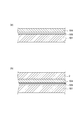
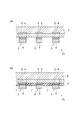
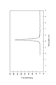
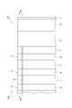
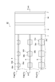
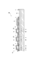
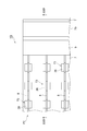
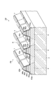
- FIG. 2 is a cross-sectional view taken along the line II-II in FIG. It is a fragmentary sectional view which shows the manufacturing process of the photodetector of FIG. It is a fragmentary sectional view which shows the manufacturing process of the photodetector of FIG. It is a fragmentary sectional view which shows the manufacturing process of the photodetector of FIG. It is a fragmentary sectional view which shows the manufacturing process of the photodetector of FIG. It is a fragmentary sectional view which shows the manufacturing process of the photodetector of FIG. It is a graph which shows the result of the simulation regarding the electric field enhancement effect by the photodetector of FIG.
- FIG. 12 is a cross-sectional view taken along line XII-XII in FIG. It is a partial top view of the photodetector of the 2nd Embodiment of this invention. It is sectional drawing along the XIV-XIV line
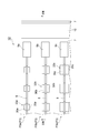
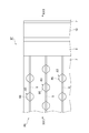
- FIG. 16 is a cross-sectional view taken along line XVI-XVI in FIG. 15. It is a partial top view of the photodetector of the 4th Embodiment of this invention.
- FIG. 18 is a sectional view taken along line XVIII-XVIII in FIG. It is a partial top view of the photodetector of the 5th Embodiment of this invention.
- FIG. 19 is a sectional view taken along line XX-XX in FIG. It is a partial top view of the photodetector of the 6th Embodiment of this invention.
- FIG. 16 is a cross-sectional view taken along line XVI-XVI in FIG. 15. It is a partial top view of the photodetector of the 4th Embodiment of this invention.
- FIG. 18 is a sectional view taken along line XVIII-XVIII in FIG. It is a partial top view of the photodetector of the 5th Embodiment of this invention.
- FIG. 20 is a cross-sectional view taken along line XXII-XXII in FIG. It is a partial top view of the photodetector of the 7th Embodiment of this invention.
- FIG. 24 is a sectional view taken along line XXIV-XXIV in FIG. It is a perspective sectional view of the photodetector of an 8th embodiment of the present invention. It is a perspective sectional view of the photodetector of the 9th embodiment of the present invention. It is a fragmentary top view of the photodetector of other embodiments of the present invention.
- FIG. 28 is a sectional view taken along line XXVIII-XXVIII in FIG. 27.
- the photodetector 1A includes a substrate 2 made of a semiconductor such as InP, GaAs, or Si or SiO 2 (glass), and a laminated structure 3 is formed on the main surface 2a. Multiple sequences are arranged.
- the laminated structure 3 is laminated on a first metal layer (first layer) 4 made of a first metal such as Au, Ag, Al, etc., and on the first metal layer 4, and incident light and accompanying light
- the plurality of stacked structures 3 are periodically patterned in a stripe shape in plan view along a plane perpendicular to the stacking direction of the first metal layer 4, the semiconductor structure layer 5, and the second metal layer 6 on the substrate 2. Arranged to form P1. That is, the periodic pattern P1 is patterned in a one-dimensional direction along a plane perpendicular to the stacking direction of the stacked structure 3.
- the semiconductor structure layer 5 has quantum intersubband levels designed according to the wavelength of light to be detected. Specifically, the semiconductor structure layer 5 is composed of InGaAs and InAlAs or InP having different energy band gaps.
- the semiconductor layer has a QWIP structure or a QCD structure in which a thickness of several nm per layer is alternately stacked.
- the first metal layer 4 is integrally formed over the plurality of laminated structures 3.
- the first metal layer 4 also functions as a common electrode for taking out electrons excited by plasmon resonance to the outside.
- SiO 2 or An insulating layer 7 made of Si 3 N 4 or the like is formed in the region on the first metal layer 4 that is integrally formed and in which the second metal layer 6 and the semiconductor structure layer 5 are not stacked (that is, the region between the stacked structures 3). Then, wiring electrodes 8 made of Au, Ti / Au, or the like are extended so as to sandwich the exposed surface of the second metal layer 6 and the exposed surface of each insulating layer 7 in each laminated structure 3. The second metal layers 6 are electrically connected.
- An extraction electrode (second electrode pad portion) 9 for taking out electrons excited by plasmon resonance to the outside is electrically connected to one end of the wiring electrode 8.
- the photodetector 1A includes a ground electrode portion (first electrode pad portion) in a region where the periodic pattern P1 is not formed, where the first metal layer 4 is viewed from a part of the insulating layer 7 in a plan view. ) 10.
- the ground electrode portion 10 is configured such that the first metal layer 4 is set to the ground potential, and a bias voltage can be applied between the extraction electrode 9 as necessary.
- a semiconductor quantum subband structure 105 made of InGaAs and InAlAs or InP having a thickness of about several nm is formed on a temporary semiconductor substrate 101 such as InP by MBE, MOCVD, or the like. Alternate epitaxial growth using the method.
- the semiconductor quantum subband structure 105 to be grown here is designed in advance so as to be optimized according to the target wavelength or the like.
- the first metal film 104 is formed on the semiconductor quantum subband structure 105 by vacuum vapor deposition, sputtering, or the like.
- the surface of the first metal film 104 is made of a semiconductor such as InP, GaAs, Si or the like for maintaining the mechanical strength of the photodetector 1A or SiO 2 ( A substrate 2 such as glass) is bonded.
- the semiconductor temporary substrate 101 is removed by polishing, chemical etching, or the like.
- an etching stop layer or a sacrificial layer may be formed in advance by a known method.
- a second metal film 106 is formed on the surface of the semiconductor quantum subband structure 105 that appears by removing the semiconductor temporary substrate 101, and FIG.
- the second metal film 106 and the semiconductor quantum subband structure 105 are partially etched by a lithography method to form a stack composed of the first metal layer 4, the semiconductor structure layer 5, and the second metal layer 6.
- a plurality of structures 3 are formed, and a striped periodic pattern P1 is formed.
- the insulating film 7 is formed in the region between the adjacent laminated structures 3, and then the wiring electrode 8 and the extraction electrode 9 are formed as shown in FIG.
- the photodetector 1A is obtained.
- each of the laminated structures 3 functions as a cavity that causes surface plasmon resonance.
- light polarized in the width direction of the cavity that is, in this embodiment, the one-dimensional direction in which the striped periodic patterns P1 are arranged in FIG. 1 is incident
- surface plasmons are excited in the laminated structure 3. Is done.
- the excited surface plasmon generates a standing wave in the laminated structure 3 by plasmon resonance, and thereby the electric field is enhanced.
- the laminated structure 3 acts as an optical antenna.
- the photodetector 1A has high photosensitivity as a photodetector using a semiconductor structure that can utilize light absorption of quantum intersubband transition.
- a photodetector that employs a QWIP structure or a QCD structure in which semiconductor layers having different energy band gaps are alternately stacked as a semiconductor structure layer is generally used for light that does not have an electric field component in the stacking direction (semiconductor structure). It does not have photosensitivity with respect to a plane wave incident from the stacking direction of the layers.
- the standing wave is generated by the plasmon resonance, whereby the electric field is enhanced and the electric field component (electric field) in the stacking direction that the incident light originally did not have. Also occurs. As a result, a very large electric field component in the stacking direction is generated, so that the photodetector 1A can detect light having no electric field component in the stacking direction before incidence.
- each of the laminated structures 3 individually acts as a cavity that causes plasmon resonance.
- the wavelength range of the light detected by this is determined by the shape and structure of the laminated structure 3.
- a light receiving area capable of detecting light is large, and the light sensitivity of the photodetector is high. It is expensive.
- the total thickness of the laminated structure of the semiconductor structure layer 5 was about 50 nm, and the period of the periodic pattern was 1 ⁇ m.
- Au was set as the metal of the first metal layer 4 and the second metal layer 6, and the wavelength of incident light was 5 ⁇ m.
- 2 ) (vertical axis) shows the maximum value when the width (horizontal axis) is 0.5 ⁇ m, and the factor of the electric field intensity, that is, the magnitude of energy, is 30 of the incident light by plasmon resonance You can see that it has more than doubled.
- L is the width of the second metal layer 6 along a predetermined direction (here, a direction perpendicular to the longitudinal direction of the multilayer structure 3) at the interface between the semiconductor structure layer 5 and the second metal layer 6.
- ⁇ p is the plasmon wavelength
- ⁇ 0 is the vacuum wavelength of the incident light
- n eff is the effective refractive index of the semiconductor quantum subband structure
- n is the refractive index of the semiconductor quantum subband structure
- ⁇ represents the skin depth of the metal
- T represents the film thickness of the semiconductor quantum subband structure.
- the laminated structure 3 having a length L in the direction perpendicular to the stacking direction, operates as a resonator of the surface plasmon wavelength lambda p that has been excited by the incident light, having a specific wavelength Only light is causing the phenomenon of enhancing the electric field.
- the wavelength of the surface plasmon standing wave excited by this is “twice the resonator length” or an integral fraction of “twice the resonator length”.
- the laminated structure 3 is striped. In the case of being formed and arranged in an island shape instead, it is necessary to adopt an effective resonator length as L in the application of the above formulas (1) to (3).
- FIG. 8 shows the result of the simulation. This is the same as the refractive index of the quantum well structure at a wavelength of 5 ⁇ m, and the strength of the electric field vector in the stacking direction for a 0.5 ⁇ m wide resonator having a dielectric having a refractive index of 3.4 sandwiched between Au ( It is the result of calculating the incident light wavelength dependency of
- the laminated structure subjected to the above simulation was actually produced, and the spectral sensitivity was measured at a temperature of 77K.
- the results are shown in the graph of FIG.
- the horizontal axis represents the wavelength of incident light, and the vertical axis represents the generated photocurrent (a.u.). According to this graph, it can be confirmed that photosensitivity is obtained with respect to light incident in the stacking direction.
- QCD was used as the semiconductor structure layer.
- the reflection spectrum of the plasmon resonator was simulated by changing the resonator length from 0.45 ⁇ m to 0.55 ⁇ m. The results are shown in the graph of FIG. From this graph, it can be seen that the light absorbed by the plasmon resonator has a reflectivity of almost zero at the resonance wavelength, and the peak of the absorbed wavelength changes by changing the resonator length.
- the semiconductor structure layer 5 is shown to be formed separately for each of the plurality of stacked structures 3, but the semiconductor structure layer 5 is shown in FIG. As shown in FIG. 12, the laminated structures 3 may be continuously formed. Thus, even when the semiconductor structure layers are continuously formed, it is confirmed from the result of simulation that the same effect as the photodetector 1A of the first embodiment can be obtained.
- the photodetector 1 ⁇ / b> B according to the second embodiment differs from the photodetector 1 ⁇ / b> A according to the first embodiment in the shape and arrangement of the stacked structure in plan view.
- the plurality of laminated structures 23 in the photodetector 1B each have a second metal layer 26 and a semiconductor structure layer 25 that are square in plan view, and are arranged in an island shape and a square lattice shape so that the periodicity is obtained.
- a pattern P2 is configured. That is, the periodic pattern P2 is patterned in a two-dimensional direction along a plane perpendicular to the stacking direction of the stacked structure 23.
- the direction that can act as a cavity that causes surface plasmon resonance is only one direction (the direction in which the striped periodic patterns P1 are arranged).
- the photodetector 1B of the second embodiment includes the second metal layer 26 and the semiconductor structure layer 25. Since the planar structure is square, the laminated structure 23 can act as a cavity that causes surface plasmon resonance at least in a direction (two directions) connecting opposite sides of the square. That is, the photodetector 1B is advantageous in that it has photosensitivity in two directions orthogonal to each other on the square surface.
- the photodetector 1 ⁇ / b> C according to the third embodiment is different from the photodetector 1 ⁇ / b> B according to the second embodiment in that it includes a multilayer structure having a plurality of sizes. .
- the periodic pattern P3 in the photodetector 1C includes a plurality of periodic pattern portions P3a, P3b, and P3c having different sizes of the second metal layers 36a, 36b, and 36c and the semiconductor structure layers 35a, 35b, and 35c. That is, as shown in FIG. 15, the stacked structures 33a, 33b, and 33c are distinguished by the different sizes of the second metal layers 36a, 36b, and 36c and the semiconductor structure layers 35a, 35b, and 35c.
- a first periodic pattern portion P3a, a second periodic pattern portion P3b, and a third periodic pattern portion P3c are formed, and each periodic pattern portion P3a, P3b, P3c is a stacked structure of stacked structures 33a, 33b, 33c. Each is patterned in a one-dimensional direction along a plane perpendicular to the direction.
- the wiring electrode 8 is wired for each of the periodic pattern portions P3a, P3b, and P3c, and all are electrically connected to the common
- the electric field enhancement effect depends on the width formed by the second metal layers 36a, 36b, and 36c and the semiconductor structure layers 35a, 35b, and 35c. More specifically, among the widths formed by the second metal layers 36a, 36b, and 36c at the interfaces between the second metal layers 36a, 36b, and 36c and the semiconductor structure layers 35a, 35b, and 35c, surface plasmon resonance is performed. Depends on the width (resonator length) that can act as a cavity to cause. For this reason, the photodetector 1A of the first embodiment including only one type of laminated structure 3 and the photodetector 1B of the second embodiment have a narrow wavelength band having high photosensitivity.
- the photodetector 1C according to this embodiment having a plurality of sizes of laminated structures has a plurality of “widths” that can act as the cavities, and thus has a wide wavelength band with high photosensitivity. That is, in the photodetector 1C according to the present embodiment, the width formed by the second metal layers 36a, 36b, and 36c at the interface between the second metal layers 36a, 36b, and 36c and the semiconductor structure layers 35a, 35b, and 35c. Among them, the surface plasmon is excited by light having a wavelength band corresponding to the width that can act as a cavity that causes surface plasmon resonance, and the electrons excited by the plasmon resonance are extracted from the common extraction electrode 9 as one output.
- this photodetector 1C light having a wide wavelength band can be detected with high photosensitivity. It is theoretically proved that even when the laminated structures 33a, 33b, and 33c having different sizes are formed adjacent to each other, plasmon resonance is not hindered.
- each periodic pattern portion has been patterned in a one-dimensional direction. However, these may be patterned in a two-dimensional direction.
- the wiring electrode 8 is shown to be wired for each of the periodic pattern portions P3a, P3b, and P3c. However, the wiring electrode 8 is wired so as to cross between different periodic pattern portions. It may be.
- the photodetector 1D of the fourth embodiment has a plurality of extraction electrodes and a plurality of periodic pattern portions P3a as compared with the photodetector 1C of the third embodiment.
- P3b and P3c are electrically connected to different extraction electrodes 9a, 9b and 9c.
- this photodetector 1D light having a different wavelength band is detected for each of the extraction electrodes 9a, 9b, and 9c. Therefore, light having a wide wavelength band is dispersed for each wavelength band and detected with high photosensitivity. can do.
- each periodic pattern portion is patterned in a one-dimensional direction. However, these may be patterned in a two-dimensional direction.
- the photodetector 1 ⁇ / b> E according to the fifth embodiment is a semiconductor structure layer 55 constituting the stacked structure 53, as compared with the photodetector 1 ⁇ / b> A according to the first embodiment.
- the difference is that the QDIP structure is adopted instead of the QWIP structure or the QCD structure.
- the QDIP structure When detecting light by the QDIP structure, unlike the QWIP structure or the QCD structure, since the light confinement direction is three-dimensional, the polarization dependence disappears, and the light is detected regardless of the vibration direction of the electric field of the light. be able to.
- the QDIP structure has a disadvantage that the light sensitivity is essentially low due to the structure.
- the electric field is enhanced in the stacked structure 53 by plasmon resonance, so that the light sensitivity is high. .
- FIGS. 21 and 22 Another embodiment of the photodetector will be described as the sixth embodiment of the present invention. As illustrated in FIGS. 21 and 22, the photodetector 1F according to the sixth embodiment differs from the photodetector 1B according to the second embodiment in the shape and arrangement of the laminated structure in plan view.
- the second metal layer 66 and the semiconductor structure layer 65 are circular in plan view, and these are arranged in an island shape and a triangular lattice shape.
- the periodic pattern P6 is configured.
- the photosensitivity is high only when the incident light has a specific polarization direction (that is, when the vibration direction of the electric field is a specific direction), whereas this embodiment In the photodetector 1F, the dependence of the incident light on the polarization direction of the light sensitivity is small.
- FIGS. 23 and 24 Another embodiment of the photodetector will be described as the seventh embodiment of the present invention.
- the photodetector 1G of the seventh embodiment is replaced with the substrate 2 and the first metal layer 4 as compared with the photodetector 1B of the second embodiment.
- the difference is that a semiconductor layer 74 doped with a high impurity is provided.
- the extraction electrode 79 is provided in the portion which is the ground electrode portion 10 in the photodetector 1B of the second embodiment.
- the semiconductor layer 74 is made of a semiconductor such as InP doped with high impurity such as Si or Zn. It is well known that highly doped semiconductors have a negative dielectric constant for mid-infrared as well as metals (for example, D. Li, C. Z. Ning, “All-semiconductor active plasmonic system in mid-infrared wavelengths ", Opt. Express, 19, 14594 (2011). For this reason, it is possible for incident mid-infrared rays to combine with surface plasmons in the laminated structure 73 to cause plasmon resonance. As a result, it is possible to obtain photosensitivity with respect to incident light in the same manner as in Example 1. In the manufacture of the photodetector 1G, a step of bonding substrates as shown in FIG. Since it is not necessary, it is easy to manufacture.
- the same height as that used for the semiconductor layer 74 is used on the semiconductor structure layer 25 in place of the second metal such as Au, Ag, or Al.
- a semiconductor doped with impurities may be stacked.
- a highly doped semiconductor layer can be used instead of the second metal. In this case, the manufacture of the photodetector 1G becomes easier.
- the photodetector 1H according to the eighth embodiment includes the first or second metal layer and the semiconductor structure layer as compared with the photodetector 1A according to the first embodiment. The difference is that a plurality of layers are provided, and the laminated structure is trapezoidal in cross section.
- a laminated structure 83a is formed by the first metal layer 4, the semiconductor structure layer 85a, and the second metal layer 86a that are sequentially laminated on the substrate 2 from the substrate 2 side. ing.
- the second metal layer 86a, the semiconductor structure layer 85b, and the second metal layer 86b form another stacked structure 83b.
- the second metal layer 86a is also used between the stacked structure 83a and the stacked structure 83b, and the second metal layer 86a is a first metal as a configuration of the stacked structure 83b. Acts as a layer.
- the plurality of stacked structures 83a and 83b are stacked on the substrate 2 in the stacking direction of the first metal layer 4, the semiconductor structure layer 85a, the second metal layer 86a, the semiconductor structure layer 85b, and the second metal layer 86b.
- the periodic patterns P8 are arranged in a stripe shape in plan view along a plane perpendicular to the vertical direction. That is, the periodic pattern P8 is patterned in a one-dimensional direction along a plane perpendicular to the stacking direction of the stacked structures 83a and 83b.
- the first metal layer 4, the semiconductor structure layer 85a, the second metal layer 86a, the semiconductor structure layer 85b, and the second metal layer 86b are arranged in this order (as they move away from the substrate 2).
- the width in the direction in which the stripes forming P8 are arranged gradually decreases, and the stacked structures 83a and 83b are both trapezoidal in cross-section.
- the laminated structures 83a and 83b are formed so as to have a trapezoidal shape in cross section even when they are regarded as one laminated structure.
- the photodetector 1H can be manufactured by the same method as the photodetector 1A of the first embodiment.
- the electric field enhancement effect and reflectivity as shown in FIGS. 7 to 10 can be obtained. That is, the laminated structures 83a and 83b configured as described above function independently as cavities that cause surface plasmon resonance. Further, as described above, since the stacked structures 83a and 83b have different widths (resonator lengths) in the direction in which the stripes forming the periodic pattern P8 are arranged in FIG. 25, the wavelength of the surface plasmon resonating in each cavity is also different. Different from each other. Therefore, there are two types of wavelengths of incident light that can excite surface plasmons that resonate in each cavity. Therefore, the photodetector 1H has high photosensitivity for two types of light having different wavelengths.
- the striped periodic pattern is arranged.
- the stacked structure is arranged in a two-dimensional direction. It may be patterned.
- the two-dimensionally arranged laminated structure may have a circular shape in plan view as in the photodetector 1F of the sixth embodiment, and may have a tapered cylindrical shape.
- the high impurity doping used in the photodetector 1G of the seventh embodiment is used on the semiconductor layer structure layers 85a and 85b in place of the second metal such as Au, Ag, and Al.
- the second metal such as Au, Ag, and Al.
- stacked semiconductors may be stacked.
- the types of wavelengths of incident light at which the photodetector 1H has photosensitivity also increase.
- the photodetector 1I of the ninth embodiment has a laminated structure that is not a trapezoidal cross-sectional view but a rectangular cross-sectional view as compared with the photodetector 1H of the eighth embodiment. The difference is that the thicknesses of the semiconductor structure layers are different from each other in the stacked structures stacked on each other.
- a laminated structure 93a is formed by the first metal layer 4, the semiconductor structure layer 95a, and the second metal layer 96a that are sequentially laminated on the substrate 2 from the substrate 2 side. ing.
- the second metal layer 96a, the semiconductor structure layer 95b, and the second metal layer 96b form another stacked structure 93b.
- the second metal layer 96a is also used between the stacked structure 93a and the stacked structure 93b, and the second metal layer 96a is the first metal as a configuration of the stacked structure 93b. Acts as a layer.
- the plurality of stacked structures 93a and 93b are stacked on the substrate 2 in the stacking direction of the first metal layer 94, the semiconductor structure layer 95a, the second metal layer 96a, the semiconductor structure layer 95b, and the second metal layer 96b.
- the periodic patterns P9 are arranged in a stripe shape in plan view along a plane perpendicular to the vertical direction. That is, the periodic pattern P9 is patterned in a one-dimensional direction along a plane perpendicular to the stacking direction of the stacked structures 93a and 93b.
- the first metal layer 4, the semiconductor structure layer 95a, the second metal layer 96a, the semiconductor structure layer 95b, and the second metal layer 96b are all in the direction in which the stripes forming the periodic pattern P9 are arranged.
- the width is the same.
- the photodetector according to the eighth embodiment has high photosensitivity for a plurality of incident lights having different wavelengths by making the cavity lengths of the cavities causing surface plasmon resonance different. Unlike 1H, by making the thickness of the resonator, specifically, the thickness of the semiconductor structure layers 95a and 95b different from each other, the photosensitivity is increased for a plurality of incident lights having different wavelengths. Yes. That is, since the stacked structures 93a and 93b in the photodetector 1I have only one type of width (resonator length) in the direction in which the stripes forming the periodic pattern P9 are arranged, the surface plasmons that resonate in both cavities are present.
- the wavelengths can be said to be the same, according to the above formulas (1) to (3), the wavelength of the incident light that can excite the surface plasmon also depends on the thickness of the semiconductor structure layers 95a and 95b. Therefore, by making the thicknesses of the semiconductor structure layers 95a and 95b different, the wavelength of the incident light that excites the surface plasmons of the specific wavelength can be made different. Therefore, the photodetector 1I has high photosensitivity for two types of light having different wavelengths.
- the present invention has been described above, but the present invention is not limited to the above embodiment.
- the stacked structure is shown so that a periodic pattern is formed by at least the second metal layer.
- the pattern may not be periodic.
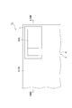
- the laminated structure acts as a cavity that causes plasmon resonance alone, the number of laminated structures may be one as in the photodetector 1J shown in FIGS. 27 and 28, for example.
- the wiring electrode 8 also serves as the extraction electrode 9, and the first metal layer 4 also serves as the ground electrode 10.
- the width of the cavity in the stacked structure 3 that is, the second along the predetermined direction (here, the direction perpendicular to the longitudinal direction of the stacked structure 3) at the interface between the semiconductor structure layer 5 and the second metal layer 6.
- the width of the metal layer 6 is an integral multiple of “half the wavelength of the excited surface plasmon” or “half the wavelength of the excited surface plasmon” 3 operates as a resonator.
- the modes shown as the first to ninth embodiments can be freely combined to constitute a photodetector.
- the semiconductor structure layer 55 (QDIP structure) in the photodetector 1E of the fifth embodiment may be applied to the photodetectors of other embodiments.
- the semiconductor doped with a high impurity in the photodetector 1G of the seventh embodiment may be applied to the photodetectors of other embodiments.
- the surface of the 1st metal layer 4 or the semiconductor layer 74 had comprised the uniform plane
- the surface is laminated
- Electrode pad portion 10 ... ground electrode portion (first electrode pad portion), 74 ... semiconductor layer (first layer), P1, P2, P3, P6, P8, P9 ... periodic pattern, P3a, P3b, P3c: Periodic pattern portion.
Landscapes
- Chemical & Material Sciences (AREA)
- Engineering & Computer Science (AREA)
- Nanotechnology (AREA)
- Physics & Mathematics (AREA)
- Life Sciences & Earth Sciences (AREA)
- Biophysics (AREA)
- Optics & Photonics (AREA)
- Crystallography & Structural Chemistry (AREA)
- Light Receiving Elements (AREA)
Description
本発明は、プラズモン共鳴を利用する光検出器に関する。
量子サブバンド間遷移の光吸収を利用する光検出器として、QWIP(量子井戸型赤外光センサ)、QCD(量子カスケード型光センサ)、QDIP(量子ドット赤外光センサ)等が知られている。これらはエネルギーバンドギャップ遷移を利用しないため、波長範囲の設計自由度が大きい、高速応答が可能である等のメリットを有する。
これらの光検出器のうち、QWIPとQCDは、半導体構造体として、量子井戸構造や量子カスケード構造等の周期的な積層構造を有する半導体積層体を備えている。この半導体積層体は、入射する光が半導体積層体の積層方向の電界成分を有する場合にのみ当該電界成分によって電流を生じるため、当該積層方向の電界成分を有しない光(半導体積層体の積層方向から入射する平面波)に対しては光感度を有しない。
従って、QWIP又はQCDで光を検出するには、光の電界の振動方向が半導体積層体の積層方向と一致するように光を入射させる必要がある。例えば、光の進行方向に垂直な波面を有する平面波を検出する場合では、光を半導体積層体の積層方向と垂直な方向から入射させる必要があるため、光検出器としての使用が煩わしいものとなる。
そこで、半導体積層体の積層方向の電界成分を有しない光を検出するために、半導体積層体の表面に金の薄膜を設け、この薄膜に当該光の波長以下の直径を有する孔を周期的に形成した光検出器が知られている(非特許文献1参照)。この例では、金の薄膜における表面プラズモンの共鳴効果によって、半導体積層体の積層方向の電界成分を有するように光を変調している。
また、プラズモン共鳴に関するものとして、絶縁体を金属で挟んだいわゆるMIM構造に光が入射した場合に、プラズモン共鳴により電場が著しく増強されることが知られている(非特許文献2参照)。
一方、QDIPについては、光の閉じ込め方向が三次元であることから偏光依存性が消失し、光の電界の振動方向に依らずに光を検出することができる。ただし、QDIPはその構造上、本質的に光感度が低いという欠点がある。
W. Wu, et al.,"Plasmonic enhanced quantum well infrared photodetector with highdetectivity", Appl. Phys. Lett., 96, 161107 (2010).
H. T. Miyazaki,Y. Kurokawa, "Squeezing Visible Light Waves into a 3-nm-Thick and 55-nm-LongPlasmon Cavity", Phys. Rev. Lett., 96, 097401 (2006).
このように、従来、特定の電界成分を有するように光を変調したり、電場を増強したりする技術が種々提案されている。その一方で、量子サブバンド間遷移の光吸収を利用するQWIP、QCD及びQDIP等の光検出器は、上記のとおり種々のメリットを有するものであるため、その光感度を高めることが求められている。
そこで、本発明は、量子サブバンド間遷移の光吸収を利用し得る半導体構造体を用いた光感度の高い光検出器を提供することを目的とする。
本発明の光検出器は、第1の金属又は第1の半導体からなる第1の層と、第1の層上に積層され、プラズモン共鳴により電子が励起される半導体構造体層と、半導体構造体層上に積層され、第2の金属又は第2の半導体からなる第2の層と、を有する積層構造体を備える。
この光検出器では、積層構造体が表面プラズモン共鳴を引き起こすキャビティとして作用する。このキャビティの幅方向に偏光した光が入射した場合に、積層構造体において表面プラズモンが励起される。励起された表面プラズモンは、プラズモン共鳴により積層構造体内において定在波を生じ、これにより電場が増強される。そして、この電界成分により半導体構造体層において電子が励起され、これが電流として検出される。従って、この光検出器は、量子サブバンド間遷移の光吸収を利用し得る半導体構造体を用いた光検出器として、光感度が高いものとなる。
ここで、半導体構造体は、量子サブバンド間遷移の光吸収が生じるものであってもよい。この場合、エネルギーバンドギャップ遷移を利用しないため、光検出器が、検出する波長範囲の設計自由度が大きく、伝導電子の走行速度が速いことから高速応答が可能なものとなる。
積層構造体は、第1の層、半導体構造体層及び第2の層の積層方向に垂直な面に沿って複数配列されていてもよい。積層構造体が複数配列されると受光領域が大きくなるため、光検出器の光感度が高いものとなる。
ここで、第1の層は複数の積層構造体にわたって一体的に形成されていてもよい。これによれば、積層構造体の配列が安定化されると共に、第1の層を共通電極として機能させることができる。
一方、半導体構造体層は、複数の積層構造体ごとに分離して形成されていてもよく、複数の積層構造体にわたって連続して形成されていてもよい。いずれの構成としても、入射した光の電場を増強することができ、光感度の高い光検出器を提供することができる。従って、光検出器の製造方法の都合等により、半導体構造体層をいずれの構成とするかを選択することができる。
また、本発明の光検出器は、プラズモン共鳴により励起された電子を外部に取り出すための第1の電極パッド部及び第2の電極パッド部を更に備え、複数の積層構造体は、少なくとも半導体構造体層と第2の層との界面における所定の方向に沿った第2の層の幅が互いに異なる第1の積層構造体及び第2の積層構造体を含み、第1の層は、第1の電極パッド部と電気的に接続されており、第1の積層構造体の第2の層、及び第2の積層構造体の第2の層は、共通の第2の電極パッド部と電気的に接続されていてもよい。この光検出器では、少なくとも半導体構造体層と第2の層との界面における所定の方向に沿った第2の層の幅が互いに異なる第1の積層構造体及び第2の積層構造体を含んでいるため、これらの幅に応じた波長帯域の光によって表面プラズモンがそれぞれ励起され、プラズモン共鳴により励起された電子を共通の第2の電極パッド部から一出力として取り出す。従って、この光検出器によれば、広い波長帯域を有する光を高い光感度で検出することができる。
また、本発明の光検出器は、プラズモン共鳴により励起された電子を外部に取り出すための第1の電極パッド部及び複数の第2の電極パッド部を更に備え、複数の積層構造体は、少なくとも半導体構造体層と第2の層との界面における所定の方向に沿った第2の層の幅が互いに異なる第1の積層構造体及び第2の積層構造体を含み、第1の層は、第1の電極パッド部と電気的に接続されており、第1の積層構造体の第2の層、及び第2の積層構造体の第2の層は、互いに異なる第2の電極パッド部と電気的に接続されていてもよい。この光検出器では、少なくとも半導体構造体層と第2の層との界面における所定の方向に沿った第2の層の幅が互いに異なる第1の積層構造体及び第2の積層構造体を含んでいるため、これらの幅に応じた波長帯域の光によって表面プラズモンが励起され、プラズモン共鳴により励起された電子を互いに異なる第2の電極パッド部から別出力として取り出す。従って、この光検出器によれば、広い波長帯域を有する光を波長帯域ごとに分光して高い光感度で検出することができる。
本発明によれば、量子サブバンド間遷移の光吸収を利用し得る半導体構造体を用いた光感度の高い光検出器を提供することができる。
以下、本発明の好適な実施形態について、図面を参照しながら詳細に説明する。なお、各図において同一部分又は相当部分には同一符号を付し、重複する説明は省略する。
[第1の実施形態]
図1及び図2に示されるように、光検出器1Aは、InP、GaAs、Si等の半導体製又はSiO2(ガラス)製の基板2を備え、この主面2a上に積層構造体3が複数配列されている。
図1及び図2に示されるように、光検出器1Aは、InP、GaAs、Si等の半導体製又はSiO2(ガラス)製の基板2を備え、この主面2a上に積層構造体3が複数配列されている。
積層構造体3は、Au、Ag、Al等の第1の金属からなる第1の金属層(第1の層)4と、第1の金属層4上に積層され、光の入射とそれに伴うプラズモン共鳴により電子が励起される半導体構造体層5と、半導体構造体層5上に積層され、Au、Ag、Al等の第2の金属からなる第2の金属層(第2の層)6とからなる。複数の積層構造体3は、基板2上において、第1の金属層4、半導体構造体層5及び第2の金属層6の積層方向に垂直な面に沿って、平面視ストライプ状に周期パターンP1が形成されるように配列されている。つまり、周期パターンP1は、積層構造体3の積層方向に垂直な面に沿って一次元方向にパターン化されている。
半導体構造体層5は、検出しようとする光の波長に合わせて設計された量子サブバンド間準位を有するものであり、具体的には、互いにエネルギーバンドギャップの異なるInGaAsとInAlAs又はInPとの半導体層が、一層あたり数nmの厚さで交互に積層されたQWIP構造又はQCD構造をなしている。
第1の金属層4は、複数の積層構造体3にわたって一体的に形成されている。この第1の金属層4は、プラズモン共鳴により励起された電子を外部に取り出すための共通電極としての機能を兼ねている。
一体成形された第1の金属層4上であり、且つ第2の金属層6及び半導体構造体層5が積層されていない領域(つまり、積層構造体3間の領域)には、SiO2又はSi3N4等からなる絶縁層7が形成されている。そして、それぞれの積層構造体3における第2の金属層6の露出表面、及び、それぞれの絶縁層7の露出表面を這うようにしてAu又はTi/Au等からなる配線電極8が延設され、それぞれの第2の金属層6間を電気的に接続している。
配線電極8の一端には、プラズモン共鳴により励起された電子を外部に取り出すための取出し電極(第2の電極パッド部)9が電気的に接続されている。また、光検出器1Aは、周期パターンP1が形成されていない領域において、平面視で絶縁層7の一部から第1の金属層4が覗いた部分を接地電極部(第1の電極パッド部)10として有している。接地電極部10は、第1の金属層4を接地電位とし、必要に応じて取出し電極9との間にバイアス電圧を印加することができるように構成されている。
次に、光検出器1Aの製造方法を説明する。図3(a)に示されるように、InP等の半導体仮基板101上に、数nm程度の厚さのInGaAsとInAlAs又はInPとからなる半導体量子サブバンド構造体105を、MBEやMOCVD等の方法を用いて交互にエピタキシャル成長させる。ここで成長させる半導体量子サブバンド構造体105は、目的とする波長等に応じて最適となるようにあらかじめ設計されたものである。そして、半導体量子サブバンド構造体105の上に、真空蒸着法やスパッタ法等により第1の金属膜104を成膜する。
次に、図3(b)に示されるように、第1の金属膜104の表面に、光検出器1Aの機械的強度を保持するためのInP、GaAs、Si等の半導体製又はSiO2(ガラス)等の基板2を貼り合わせる。そして、図4(a)に示されるように、半導体仮基板101を研磨及び化学エッチング等によって除去する。その際、半導体量子サブバンド構造体105を保持するために、周知の手法により、エッチングストップ層又は犠牲層をあらかじめ形成しておいてもよい。
次に、図4(b)に示されるように、半導体仮基板101の除去によって現れた半導体量子サブバンド構造体105の表面に第2の金属膜106を成膜し、図5(a)に示されるように、リソグラフィ法によって第2の金属膜106及び半導体量子サブバンド構造体105を部分エッチングして、第1の金属層4、半導体構造体層5及び第2の金属層6からなる積層構造体3を複数形成すると共に、ストライプ状の周期パターンP1を形成する。その後、図5(b)に示されるように、隣接する積層構造体3間の領域に絶縁膜7を形成し、次いで図6に示されるように、配線電極8及び取出し電極9を形成することで、光検出器1Aが得られる。
次に、光検出器1Aの動作原理及び作用効果を説明する。光検出器1Aでは、積層構造体3のそれぞれが、表面プラズモン共鳴を引き起こすキャビティとして作用する。このキャビティの幅方向(つまり本実施形態の場合、図1においてストライプ状の周期パターンP1が並ぶ一次元方向でもある。)に偏光した光が入射した場合に、積層構造体3において表面プラズモンが励起される。励起された表面プラズモンは、プラズモン共鳴により積層構造体3内において定在波を生じ、これにより電場が増強される。また、表面プラズモンがキャビティ内で共振することにより積層構造体3が光アンテナとして作用する結果、積層構造体3の周辺に入射する光がキャビティ内に引き込まれ、積層方向の電界成分が生じることになる。そして、この電界成分により半導体構造体層5において電子が励起され、励起された電子は配線電極8を通じて取出し電極9に集められ、外部回路に電流として出力されて光感度となる。従って、この光検出器1Aは、量子サブバンド間遷移の光吸収を利用し得る半導体構造体を用いた光検出器として、光感度が高いものとなる。
また、通常、互いにエネルギーバンドギャップの異なる半導体層が交互に積層されたQWIP構造又はQCD構造を半導体構造体層として採用する光検出器は、その積層方向の電界成分を有しない光(半導体構造体層の積層方向から入射する平面波)に対しては光感度を有しない。これに対し、本実施形態の光検出器1Aは、上記プラズモン共鳴により定在波が生じることで、電場が増強されると共に、入射光がもともと有していなかった積層方向の電界成分(電場)も生じる。その結果、非常に大きな積層方向の電界成分が発生することとなるため、光検出器1Aは、入射前に積層方向の電界成分を有しない光をも検出することができる。
光検出器1Aでは、上記のとおり、積層構造体3のそれぞれが個別にプラズモン共鳴を引き起こすキャビティとして作用する。これによって検出される光の波長範囲は、積層構造体3の形状、構造等によって決まる。この光検出器1Aは、この積層構造体3がその積層方向に垂直な面に沿って複数配列されているために、光の検出を可能とする受光領域が大きく、光検出器の光感度が高いものとなっている。
次に、プラズモン共鳴に基づく電場の増強効果に関するシミュレーションの結果を示す。光検出器1Aにおける半導体構造体層5がInGaAsとInAlAsとの積層構造からなる場合において、半導体構造体層5内に生じる積層方向の電界成分の強度を、FDTD(Finite-Difference Time-Domain;有限差分時間領域)シミュレーション法によって計算した。
パラメータとして、半導体構造体層5の積層構造の膜厚の合計を約50nm、周期パターンの周期を1μmとした。第1の金属層4及び第2の金属層6の金属としてAuを設定し、入射光の波長は5μmとした。第2の金属層6及び半導体構造体層5がなすストライプ幅を種々変更してシミュレーションを行った結果、図7に示されるように、第2の金属層6及び半導体構造体層5がなすストライプ幅(横軸)が0.5μmの時に電界強度(|Ez|2)(縦軸)が最大値を示し、プラズモン共鳴によってその電界強度の階乗、すなわちエネルギーの大きさは入射光の30倍以上に及んだことが分かる。
第2の金属層6及び半導体構造体層5がなすストライプ幅が0.5μmの時に特に電場の増強効果が高くなることは、次の式(1)~(3)を用いて説明することができる。
L=λp/2 …(1)
λp=λ0/neff …(2)
neff=n√(1+2δ/T) …(3)
ここで、Lは半導体構造体層5と第2の金属層6との界面における所定の方向(ここでは積層構造体3の長手方向に垂直な方向)に沿った第2の金属層6の幅(すなわちプラズモン共鳴を引き起こすキャビティの幅)、λpはプラズモン波長、λ0は入射光の真空波長、neffは半導体量子サブバンド構造の実効屈折率、nは半導体量子サブバンド構造の屈折率、δは金属の表皮深さ、Tは半導体量子サブバンド構造の膜厚をそれぞれ示す。これらの式に実際の値、すなわちλ0=5μm、n=3.5、δ=25nm、T=50nmを代入すると、Lは約0.5μmとなり、シミュレーション結果と一致する。この式の意味するところは、積層方向に垂直な方向の長さLをもつ積層構造体3が、入射光によって励起された波長λpの表面プラズモンの共振器として動作し、特定の波長を有する光のみが電場を増強させる現象を引き起こしているということである。すなわち、これによって励起される表面プラズモン定在波の波長は、「共振器長の2倍」、もしくは「共振器長の2倍」の整数分の1倍となる。なお、この例では、構造体が立方体の形状をしているため積層構造体3の長さLをそのまま式に代入したが、後述する他の実施形態のように、積層構造体3がストライプ状でなく島状に形成及び配列されている場合には、上記式(1)~(3)の適用においては実効的な共振器長をLとして採用する必要がある。
L=λp/2 …(1)
λp=λ0/neff …(2)
neff=n√(1+2δ/T) …(3)
ここで、Lは半導体構造体層5と第2の金属層6との界面における所定の方向(ここでは積層構造体3の長手方向に垂直な方向)に沿った第2の金属層6の幅(すなわちプラズモン共鳴を引き起こすキャビティの幅)、λpはプラズモン波長、λ0は入射光の真空波長、neffは半導体量子サブバンド構造の実効屈折率、nは半導体量子サブバンド構造の屈折率、δは金属の表皮深さ、Tは半導体量子サブバンド構造の膜厚をそれぞれ示す。これらの式に実際の値、すなわちλ0=5μm、n=3.5、δ=25nm、T=50nmを代入すると、Lは約0.5μmとなり、シミュレーション結果と一致する。この式の意味するところは、積層方向に垂直な方向の長さLをもつ積層構造体3が、入射光によって励起された波長λpの表面プラズモンの共振器として動作し、特定の波長を有する光のみが電場を増強させる現象を引き起こしているということである。すなわち、これによって励起される表面プラズモン定在波の波長は、「共振器長の2倍」、もしくは「共振器長の2倍」の整数分の1倍となる。なお、この例では、構造体が立方体の形状をしているため積層構造体3の長さLをそのまま式に代入したが、後述する他の実施形態のように、積層構造体3がストライプ状でなく島状に形成及び配列されている場合には、上記式(1)~(3)の適用においては実効的な共振器長をLとして採用する必要がある。
また、光検出器1Aについて、入射前に積層方向の電界成分を有しない光が入射した場合に、表面プラズモン共鳴を引き起こして積層方向の電界ベクトルを発生させることができることに関し、別のシミュレーションを行った。図8にそのシミュレーションの結果を示す。これは、波長5μmにおける量子井戸構造体の屈折率と同じ、屈折率3.4の誘電体がAuに挟まれた幅0.5μmのストライプ形状の共振器について、積層方向の電界ベクトルの強度(|Ez|2)の入射光波長依存性を計算した結果である。図8によれば、共鳴波長の5μmにおいて、入射光の全電界強度に対し10倍以上の電界ベクトルの強度(|Ez|2)が得られることが分かる。
上記シミュレーションを行った積層構造体を実際に作製し、温度77Kにおいて分光感度を測定した。結果を図9のグラフに示す。横軸は入射光の波長、縦軸は生じた光電流(a.u.)である。このグラフによれば、積層方向に入射した光に対して光感度が得られたことを確認することができる。ここで、半導体構造体層としてはQCDを用いた。
また、共振器長を0.45μmから0.55μmまで変化させて、プラズモン共振器の反射スペクトルをシミュレーションした。結果を図10のグラフに示す。このグラフから、プラズモン共振器に吸収される光は共鳴波長において反射率がほぼ0になること、及び、共振器長を変えることによって、吸収される波長のピークが変化することが分かる。
上記第1の実施形態の光検出器1Aでは、半導体構造体層5が複数の積層構造体3ごとに分離して形成されている態様を示したが、半導体構造体層5は、図11及び図12に示されるように、複数の積層構造体3にわたって連続して形成されていてもよい。このように半導体構造体層が連続して形成されている場合でも、シミュレーションの結果から、第1の実施形態の光検出器1Aと同等の効果が得られることが確認されている。
[第2の実施形態]
本発明の第2の実施形態として、光検出器の他の形態について説明する。図13及び図14に示されるように、第2の実施形態の光検出器1Bは、第1の実施形態の光検出器1Aと比べて、平面視における積層構造体の形状及び配列が異なる。
本発明の第2の実施形態として、光検出器の他の形態について説明する。図13及び図14に示されるように、第2の実施形態の光検出器1Bは、第1の実施形態の光検出器1Aと比べて、平面視における積層構造体の形状及び配列が異なる。
光検出器1Bにおける複数の積層構造体23は、それぞれ第2の金属層26及び半導体構造体層25が平面視正方形とされており、これらが島状且つ正方格子状に配列されることにより周期パターンP2が構成されている。つまり、周期パターンP2は、積層構造体23の積層方向に垂直な面に沿って二次元方向にパターン化されている。
第1の実施形態の光検出器1Aでは、積層構造体3において、表面プラズモン共鳴を引き起こすキャビティとして作用しうる方向が一方向(ストライプ状の周期パターンP1が並ぶ方向)のみであるために、その方向に偏光した光(その方向の電界成分を有する光)に対してのみ光感度を有するが、第2の実施形態の光検出器1Bは、第2の金属層26及び半導体構造体層25が平面視正方形とされているために、積層構造体23は、少なくともその正方形の向かい合う辺を結ぶ方向(二方向)において表面プラズモン共鳴を引き起こすキャビティとして作用しうる。すなわち、光検出器1Bは、当該正方形の面上で直交する二方向において光感度を有する点で有利である。
[第3の実施形態]
本発明の第3の実施形態として、光検出器の他の形態について説明する。図15及び図16に示されるように、第3の実施形態の光検出器1Cは、第2の実施形態の光検出器1Bと比べて、複数の大きさの積層構造体を含む点が異なる。
本発明の第3の実施形態として、光検出器の他の形態について説明する。図15及び図16に示されるように、第3の実施形態の光検出器1Cは、第2の実施形態の光検出器1Bと比べて、複数の大きさの積層構造体を含む点が異なる。
光検出器1Cにおける周期パターンP3は、第2の金属層36a,36b,36c及び半導体構造体層35a,35b,35cの大きさが異なる複数の周期パターン部P3a,P3b,P3cを含んでいる。すなわち、積層構造体33a,33b,33cは、図15に示されるように、第2の金属層36a,36b,36c及び半導体構造体層35a,35b,35cの大きさが異なることにより区別された第1の周期パターン部P3a、第2の周期パターン部P3b、及び第3の周期パターン部P3cを形成し、それぞれの周期パターン部P3a,P3b,P3cは、積層構造体33a,33b,33cの積層方向に垂直な面に沿ってそれぞれ一次元方向にパターン化されている。配線電極8は、周期パターン部P3a,P3b,P3cごとに配線されており、いずれも共通の取出し電極9と電気的に接続されている。
第1の実施形態における図7から分かるように、電場の増強効果は、第2の金属層36a,36b,36c及び半導体構造体層35a,35b,35cがなす幅に依存する。より具体的には、第2の金属層36a,36b,36cと半導体構造体層35a,35b,35cとの界面における第2の金属層36a,36b,36cがなす幅のうち、表面プラズモン共鳴を引き起こすキャビティとして作用しうる幅(共振器長)に依存する。このため、1種の積層構造体3のみを含む第1の実施形態の光検出器1A及び第2の実施形態の光検出器1Bは、高い光感度を有する波長帯域が狭い。これに対し、複数の大きさの積層構造体を有する本実施形態の光検出器1Cでは、上記キャビティとして作用しうる「幅」を複数有するため、高い光感度を有する波長帯域が広い。すなわち、本実施形態の光検出器1Cでは、第2の金属層36a,36b,36cと半導体構造体層35a,35b,35cとの界面における第2の金属層36a,36b,36cがなす幅のうち、表面プラズモン共鳴を引き起こすキャビティとして作用しうる幅に応じた波長帯域の光によって表面プラズモンが励起され、プラズモン共鳴により励起された電子を共通の取出し電極9から一出力として取り出す。従って、この光検出器1Cによれば、広い波長帯域を有する光を高い光感度で検出することができる。なお、このように大きさの異なる積層構造体33a,33b,33cが隣接して形成されている場合でも、互いのプラズモン共鳴は妨げられないことが、理論上証明されている。
なお、上記第3の実施形態の光検出器1Cでは、それぞれの周期パターン部が一次元方向にパターン化されている態様を示したが、これらが二次元方向にパターン化されていてもよい。また、上記第3の実施形態の光検出器1Cでは、配線電極8が周期パターン部P3a,P3b,P3cごとに配線された態様を示したが、異なる周期パターン部間を横断するように配線されていてもよい。
[第4の実施形態]
本発明の第4の実施形態として、光検出器の他の形態について説明する。図17及び図18に示されるように、第4の実施形態の光検出器1Dは、第3の実施形態の光検出器1Cと比べて、取出し電極が複数形成され、複数の周期パターン部P3a,P3b,P3cが互いに異なる取出し電極9a,9b,9cと電気的に接続されている点が異なる。
本発明の第4の実施形態として、光検出器の他の形態について説明する。図17及び図18に示されるように、第4の実施形態の光検出器1Dは、第3の実施形態の光検出器1Cと比べて、取出し電極が複数形成され、複数の周期パターン部P3a,P3b,P3cが互いに異なる取出し電極9a,9b,9cと電気的に接続されている点が異なる。
この光検出器1Dでは、取出し電極9a,9b,9cごとに異なる波長帯域を有する光が検出されることになるため、広い波長帯域を有する光を波長帯域ごとに分光して高い光感度で検出することができる。
なお、上記第4の実施形態の光検出器1Dでは、それぞれの周期パターン部が一次元方向にパターン化されている態様を示したが、これらが二次元方向にパターン化されていてもよい。
[第5の実施形態]
本発明の第5の実施形態として、光検出器の他の形態について説明する。図19及び図20に示されるように、第5の実施形態の光検出器1Eは、第1の実施形態の光検出器1Aと比べて、積層構造体53を構成する半導体構造体層55として、QWIP構造又はQCD構造に替えてQDIP構造が採用されている点が異なる。
本発明の第5の実施形態として、光検出器の他の形態について説明する。図19及び図20に示されるように、第5の実施形態の光検出器1Eは、第1の実施形態の光検出器1Aと比べて、積層構造体53を構成する半導体構造体層55として、QWIP構造又はQCD構造に替えてQDIP構造が採用されている点が異なる。
QDIP構造により光を検出する場合、QWIP構造又はQCD構造とは異なり、光の閉じ込め方向が三次元であることから偏光依存性が消失し、光の電界の振動方向に依らずに光を検出することができる。QDIP構造ではその構造上、本質的に光感度が低いという欠点があるが、本実施形態の光検出器1Eでは、プラズモン共鳴により積層構造体53内において電場が増強されるため、光感度が高い。
[第6の実施形態]
本発明の第6の実施形態として、光検出器の他の形態について説明する。図21及び図22に示されるように、第6の実施形態の光検出器1Fは、第2の実施形態の光検出器1Bと比べて、平面視における積層構造体の形状及び配列が異なる。
本発明の第6の実施形態として、光検出器の他の形態について説明する。図21及び図22に示されるように、第6の実施形態の光検出器1Fは、第2の実施形態の光検出器1Bと比べて、平面視における積層構造体の形状及び配列が異なる。
すなわち、光検出器1Fにおける複数の積層構造体63は、それぞれ第2の金属層66及び半導体構造体層65が平面視円形とされており、これらが島状且つ三角格子状に配列されることにより周期パターンP6が構成されている。
第2の実施形態の光検出器1Bでは、入射光が特定の偏光方向を有する場合(つまり、電界の振動方向が特定の方向である場合)にのみ光感度が高いのに対し、本実施形態の光検出器1Fでは、光感度について、入射光の偏光方向に対する依存性が小さい。
[第7の実施形態]
本発明の第7の実施形態として、光検出器の他の形態について説明する。図23及び図24に示されるように、第7の実施形態の光検出器1Gは、第2の実施形態の光検出器1Bと比べて、基板2及び第1の金属層4に替えて、高不純物ドーピングされた半導体層74を備える点が異なる。また、第2の実施形態の光検出器1Bにおいて接地電極部10とされていた部分に取出し電極79が設けられている点が異なる。
本発明の第7の実施形態として、光検出器の他の形態について説明する。図23及び図24に示されるように、第7の実施形態の光検出器1Gは、第2の実施形態の光検出器1Bと比べて、基板2及び第1の金属層4に替えて、高不純物ドーピングされた半導体層74を備える点が異なる。また、第2の実施形態の光検出器1Bにおいて接地電極部10とされていた部分に取出し電極79が設けられている点が異なる。
半導体層74は、SiやZn等が高不純物ドーピングされたInP等の半導体からなる。高不純物ドーピングされた半導体は、中赤外線に対しては金属と同様に誘電率が負となることが周知である(例えば、D. Li, C. Z. Ning, "All-semiconductor active plasmonic system
in mid-infrared wavelengths", Opt. Express, 19, 14594 (2011)参照)。このため、入射した中赤外線が積層構造体73において表面プラズモンと結合し、プラズモン共鳴を引き起こすことが可能である。その結果、第1実施例と同様にして、入射光に対して光感度を得ることができる。この光検出器1Gの製造においては、図3(b)に示されるような基板を貼り合せる工程が不要となるため、製造が簡単である。
in mid-infrared wavelengths", Opt. Express, 19, 14594 (2011)参照)。このため、入射した中赤外線が積層構造体73において表面プラズモンと結合し、プラズモン共鳴を引き起こすことが可能である。その結果、第1実施例と同様にして、入射光に対して光感度を得ることができる。この光検出器1Gの製造においては、図3(b)に示されるような基板を貼り合せる工程が不要となるため、製造が簡単である。
なお、上記第7の実施形態の光検出器1Gにおいては、半導体構造体層25上に、Au、Ag、Al等の第2の金属に替えて、半導体層74に用いたのと同様の高不純物ドーピングされた半導体を積層してもよい。上記のように、高不純物ドーピングされた半導体の誘電率が負となる波長帯域においては、高不純物ドーピングされた半導体層を第2の金属の替わりに用いることができる。この場合、光検出器1Gの製造がより簡単になる。
[第8の実施形態]
本発明の第8の実施形態として、光検出器の他の形態について説明する。図25に示されるように、第8の実施形態の光検出器1Hは、第1の実施形態の光検出器1Aと比べて、第1又は第2の金属層、及び半導体構造体層をそれぞれ複数備える点、並びに、積層構造体が断面視台形とされている点が異なる。
本発明の第8の実施形態として、光検出器の他の形態について説明する。図25に示されるように、第8の実施形態の光検出器1Hは、第1の実施形態の光検出器1Aと比べて、第1又は第2の金属層、及び半導体構造体層をそれぞれ複数備える点、並びに、積層構造体が断面視台形とされている点が異なる。
光検出器1Hでは、基板2上に基板2の側から順に積層された第1の金属層4と、半導体構造体層85aと、第2の金属層86aとにより、積層構造体83aが形成されている。また、当該第2の金属層86aと、半導体構造体層85bと、第2の金属層86bとにより、別の積層構造体83bが形成されている。ここで、積層構造体83aと積層構造体83bとの間で、第2の金属層86aは兼用されており、当該第2の金属層86aは、積層構造体83bの構成としては第1の金属層として機能する。
複数の積層構造体83a,83bは、基板2上において、第1の金属層4、半導体構造体層85a、第2の金属層86a、半導体構造体層85b及び第2の金属層86bの積層方向に垂直な面に沿って、平面視ストライプ状に周期パターンP8が形成されるようにそれぞれ配列されている。つまり、周期パターンP8は、積層構造体83a,83bの積層方向に垂直な面に沿って一次元方向にパターン化されている。また、第1の金属層4、半導体構造体層85a、第2の金属層86a、半導体構造体層85b及び第2の金属層86bは、この順に(基板2から遠ざかるにしたがって)、当該周期パターンP8を形成するストライプが並ぶ方向の幅が、徐々に小さくなっており、積層構造体83a,83bがいずれも断面視台形とされている。また、積層構造体83a,83bは、これらを一つの積層構造体とみなした場合でも断面視台形となるように形成されている。なお、光検出器1Hは、第1の実施形態の光検出器1Aと同様の方法で製造することができる。
本実施形態の光検出器1Hにおいても、図7~図10に示されたような電場の増強効果及び反射率が得られる。つまり、上記のように構成された積層構造体83a,83bは、それぞれ独立に、表面プラズモン共鳴を引き起こすキャビティとして作用する。また、積層構造体83a,83bは、上記のとおり、図25において周期パターンP8を形成するストライプが並ぶ方向の幅(共振器長)が互いに異なるため、それぞれのキャビティで共振する表面プラズモンの波長も互いに異なる。従って、それぞれのキャビティで共振する表面プラズモンを励起しうる入射光の波長は2種類存在することになる。従って、光検出器1Hは、波長の異なる2種類の光に対して光感度が高いものとなる。
なお、上記第8の実施形態の光検出器1Hでは、ストライプ状の周期パターンが並ぶ態様を示したが、第2の実施形態の光検出器1Bのように、積層構造体は二次元方向にパターン化されていてもよい。またここで、二次元に配列された積層構造体は、第6の実施形態の光検出器1Fのように平面視円形とされ、且つ、先細りの円筒形状とされていてもよい。
また、光検出器1Hにおいて、半導体層構造体層85a,85b上に、Au,Ag,Al等の第2の金属に替えて、第7の実施形態の光検出器1Gで用いた高不純物ドーピングされた半導体を積層してもよい。また、積層構造体が更に積層された態様としてもよい。積層数が増えるほど、光検出器1Hが光感度を有する入射光の波長の種類も増える。
[第9の実施形態]
本発明の第9の実施形態として、光検出器の他の形態について説明する。図26に示されるように、第9の実施形態の光検出器1Iは、第8の実施形態の光検出器1Hと比べて、積層構造体が断面視台形ではなく断面視矩形とされている点、及び、互いに積層された積層構造体において、半導体構造体層の厚さが互いに異なる点が異なる。
本発明の第9の実施形態として、光検出器の他の形態について説明する。図26に示されるように、第9の実施形態の光検出器1Iは、第8の実施形態の光検出器1Hと比べて、積層構造体が断面視台形ではなく断面視矩形とされている点、及び、互いに積層された積層構造体において、半導体構造体層の厚さが互いに異なる点が異なる。
光検出器1Iでは、基板2上に基板2の側から順に積層された第1の金属層4と、半導体構造体層95aと、第2の金属層96aとにより、積層構造体93aが形成されている。また、当該第2の金属層96aと、半導体構造体層95bと、第2の金属層96bとにより、別の積層構造体93bが形成されている。ここで、積層構造体93aと積層構造体93bとの間で、第2の金属層96aは兼用されており、当該第2の金属層96aは、積層構造体93bの構成としては第1の金属層として機能する。
複数の積層構造体93a,93bは、基板2上において、第1の金属層94、半導体構造体層95a、第2の金属層96a、半導体構造体層95b及び第2の金属層96bの積層方向に垂直な面に沿って、平面視ストライプ状に周期パターンP9が形成されるようにそれぞれ配列されている。つまり、周期パターンP9は、積層構造体93a,93bの積層方向に垂直な面に沿って一次元方向にパターン化されている。なお、第1の金属層4、半導体構造体層95a、第2の金属層96a、半導体構造体層95b及び第2の金属層96bは、いずれも当該周期パターンP9を形成するストライプが並ぶ方向の幅が同一とされている。
この光検出器1Iでは、表面プラズモン共鳴を引き起こすキャビティの共振器長を異なるものとすることによって波長が異なる複数の入射光に対して光感度を高いものとしている第8の実施形態の光検出器1Hとは異なり、共振器の厚さ、具体的には半導体構造体層95a,95bの厚さを互いに異なるものとすることによって、波長が異なる複数の入射光に対して光感度を高いものとしている。すなわち、光検出器1Iにおける積層構造体93a,93bは、いずれも周期パターンP9を形成するストライプが並ぶ方向の幅(共振器長)が1種類しか存在しないため、両キャビティで共振する表面プラズモンの波長は同一であるといえるところ、上記式(1)~(3)によれば、当該表面プラズモンを励起することができる入射光の波長は半導体構造体層95a,95bの厚さにも依存するため、半導体構造体層95a,95bの厚さを異なるものとすることによって、特定波長の表面プラズモンが励起される入射光の波長を異なるものとすることができる。従って、光検出器1Iは、波長の異なる2種類の光に対して光感度が高いものとなる。
以上、本発明の好適な実施形態について説明したが、本発明は上記実施形態に何ら限定されるものではない。例えば、上記実施形態ではいずれも、積層構造体が少なくとも第2の金属層により周期パターンが形成されるように配列された態様を示したが、パターンは周期的でなくてもよい。また、積層構造体は単独でプラズモン共鳴を引き起こすキャビティとして作用するため、例えば図27及び図28に示される光検出器1Jのように、積層構造体は一つであってもよい。ここで、配線電極8は取り出し電極9を兼ね、第1の金属層4は接地電極10を兼ねている。積層構造体3におけるキャビティの幅、すなわち半導体構造体層5と第2の金属層6との界面における所定の方向(ここでは積層構造体3の長手方向に垂直な方向)に沿った第2の金属層6の幅が、「励起される表面プラズモンの波長の2分の1倍」、もしくは「励起される表面プラズモンの波長の2分の1倍」の整数倍である場合に、積層構造体3が共振器として動作する。
また、上記第1~第9実施形態として示した態様は、それぞれ自由に組み合わせて光検出器を構成することができる。一例として、第5の実施形態の光検出器1Eにおける半導体構造体層55(QDIP構造)を、他の実施形態の光検出器に適用してもよい。また、第7の実施形態の光検出器1Gにおける高不純物ドーピングされた半導体を、他の実施形態の光検出器に適用してもよい。
また、上記実施形態においては、第1の金属層4又は半導体層74の表面が一様な平面をなしている状態を前提として記載したが、光検出器を製造する過程で、その表面が積層構造体の周期構造に即した凹凸形状となることがある。そのような形状に対しても、本発明は適用されるものである。
1A,1B,1C,1D,1E,1F,1G,1H,1I,1J…光検出器、3,23,33a,33b,33c,53,63,73,83a,83b,93a,93b…積層構造体、4…第1の金属層(第1の層)、5,25,35a,35b,35c,55,65,85a,85b,95a,95b…半導体構造体層、6,26,36a,36b,36c,66,86a,86b,96a,96b…第2の金属層(第2の層)、7…絶縁膜、8…配線電極、9,9a,9b,9c,79…取出し電極(第2の電極パッド部)、10…接地電極部(第1の電極パッド部)、74…半導体層(第1の層)、P1,P2,P3,P6,P8,P9…周期パターン、P3a,P3b,P3c…周期パターン部。
Claims (8)
- 第1の金属又は第1の半導体からなる第1の層と、
前記第1の層上に積層され、プラズモン共鳴により電子が励起される半導体構造体層と、
前記半導体構造体層上に積層され、第2の金属又は第2の半導体からなる第2の層と、を有する積層構造体を備える光検出器。 - 前記半導体構造体は、量子サブバンド間遷移の光吸収が生じるものである、請求項1記載の光検出器。
- 前記積層構造体は、前記第1の層、前記半導体構造体層及び前記第2の層の積層方向に垂直な面に沿って複数配列されている、請求項1又は2記載の光検出器。
- 前記第1の層は、複数の前記積層構造体にわたって一体的に形成されている、請求項3記載の光検出器。
- 前記半導体構造体層は、複数の前記積層構造体ごとに分離して形成されている、請求項3又は4記載の光検出器。
- 前記半導体構造体層は、複数の前記積層構造体にわたって連続して形成されている、請求項3又は4記載の光検出器。
- 前記プラズモン共鳴により励起された電子を外部に取り出すための第1の電極パッド部及び第2の電極パッド部を更に備え、
複数の前記積層構造体は、少なくとも前記半導体構造体層と前記第2の層との界面における所定の方向に沿った前記第2の層の幅が互いに異なる第1の積層構造体及び第2の積層構造体を含み、
前記第1の層は、前記第1の電極パッド部と電気的に接続されており、
前記第1の積層構造体の前記第2の層、及び前記第2の積層構造体の前記第2の層は、共通の前記第2の電極パッド部と電気的に接続されている、請求項3~6のいずれか一項記載の光検出器。 - 前記プラズモン共鳴により励起された電子を外部に取り出すための第1の電極パッド部及び複数の第2の電極パッド部を更に備え、
複数の前記積層構造体は、少なくとも前記半導体構造体層と前記第2の層との界面における所定の方向に沿った前記第2の層の幅が互いに異なる第1の積層構造体及び第2の積層構造体を含み、
前記第1の層は、前記第1の電極パッド部と電気的に接続されており、
前記第1の積層構造体の前記第2の層、及び前記第2の積層構造体の前記第2の層は、互いに異なる前記第2の電極パッド部と電気的に接続されている、請求項3~6のいずれか一項記載の光検出器。
Priority Applications (2)
| Application Number | Priority Date | Filing Date | Title |
|---|---|---|---|
| PCT/JP2013/060080 WO2013183343A1 (ja) | 2012-06-05 | 2013-04-02 | 光検出器 |
| JP2014519862A JP5869671B2 (ja) | 2012-06-05 | 2013-04-02 | 光検出器 |
Applications Claiming Priority (2)
| Application Number | Priority Date | Filing Date | Title |
|---|---|---|---|
| JP2012128069 | 2012-06-05 | ||
| JP2012-128069 | 2012-06-05 |
Publications (1)
| Publication Number | Publication Date |
|---|---|
| WO2013183178A1 true WO2013183178A1 (ja) | 2013-12-12 |
Family
ID=49669198
Family Applications (2)
| Application Number | Title | Priority Date | Filing Date |
|---|---|---|---|
| PCT/JP2012/078372 Ceased WO2013183178A1 (ja) | 2012-06-05 | 2012-11-01 | 光検出器 |
| PCT/JP2013/060080 Ceased WO2013183343A1 (ja) | 2012-06-05 | 2013-04-02 | 光検出器 |
Family Applications After (1)
| Application Number | Title | Priority Date | Filing Date |
|---|---|---|---|
| PCT/JP2013/060080 Ceased WO2013183343A1 (ja) | 2012-06-05 | 2013-04-02 | 光検出器 |
Country Status (3)
| Country | Link |
|---|---|
| US (1) | US9368661B2 (ja) |
| JP (1) | JP5869671B2 (ja) |
| WO (2) | WO2013183178A1 (ja) |
Cited By (1)
| Publication number | Priority date | Publication date | Assignee | Title |
|---|---|---|---|---|
| JP2020004775A (ja) * | 2018-06-25 | 2020-01-09 | 浜松ホトニクス株式会社 | 光検出器 |
Families Citing this family (11)
| Publication number | Priority date | Publication date | Assignee | Title |
|---|---|---|---|---|
| FR2992470B1 (fr) * | 2012-06-26 | 2014-08-08 | Commissariat Energie Atomique | Element photodetecteur pour une radiation lumineuse infrarouge et photodetecteur comprenant un tel element photodetecteur |
| US8861138B2 (en) * | 2013-03-18 | 2014-10-14 | Headway Technologies, Inc. | Multilayer plasmon generator |
| US8830799B1 (en) | 2013-03-18 | 2014-09-09 | Headway Technologies, Inc. | Near-field light generator and thermally-assisted magnetic recording head |
| US8867170B1 (en) | 2013-07-15 | 2014-10-21 | Headway Technologies, Inc. | Multilayer plasmon generator |
| WO2015104294A1 (en) * | 2014-01-07 | 2015-07-16 | Universite Paris Diderot Paris 7 | Semiconductor photodetector |
| JP7450912B2 (ja) * | 2019-12-20 | 2024-03-18 | 国立研究開発法人物質・材料研究機構 | 赤外光用検出素子および発光素子 |
| CN111192891B (zh) * | 2020-01-15 | 2023-08-04 | 宁波飞芯电子科技有限公司 | 硅光检测器、测距方法及装置 |
| CN111293188B (zh) * | 2020-02-28 | 2021-10-01 | 中国科学院上海技术物理研究所 | 一种集成式高消光比红外圆偏振探测器及设计方法 |
| FR3118020B1 (fr) * | 2020-12-23 | 2023-06-02 | Thales Sa | Planarisation de dielectrique, localisee et basse temperature |
| FR3118288B1 (fr) * | 2020-12-23 | 2022-12-30 | Thales Sa | Integration d'un circuit de detection a base de resonateurs optiques interconnectes sur un circuit de lecteure d'un imageur |
| US12681196B2 (en) * | 2021-04-22 | 2026-07-14 | Massachusetts Institute Of Technology | Methods and apparatuses for enhancing scintillation with optical nanostructures for scintillators, LEDs, and laser sources |
Citations (6)
| Publication number | Priority date | Publication date | Assignee | Title |
|---|---|---|---|---|
| JP2007266541A (ja) * | 2006-03-30 | 2007-10-11 | Fujitsu Ltd | 多波長量子井戸型赤外線検知器 |
| JP2007273832A (ja) * | 2006-03-31 | 2007-10-18 | Nec Corp | フォトダイオードとその製造方法 |
| JP2009038352A (ja) * | 2007-07-06 | 2009-02-19 | Canon Inc | 光検出素子及び撮像素子、光検出方法及び撮像方法 |
| WO2009088071A1 (ja) * | 2008-01-10 | 2009-07-16 | Nec Corporation | 半導体受光素子及び光通信デバイス |
| WO2010072942A1 (fr) * | 2008-12-24 | 2010-07-01 | Commissariat A L'energie Atomique Et Aux Energies Alternatives | Photodetecteur comprenant une region semiconductrice tres mince |
| JP2012083238A (ja) * | 2010-10-13 | 2012-04-26 | Nec Corp | 赤外線検出装置 |
Family Cites Families (14)
| Publication number | Priority date | Publication date | Assignee | Title |
|---|---|---|---|---|
| US5485015A (en) * | 1994-08-25 | 1996-01-16 | The United States Of America As Represented By The Secretary Of The Army | Quantum grid infrared photodetector |
| US6054718A (en) * | 1998-03-31 | 2000-04-25 | Lockheed Martin Corporation | Quantum well infrared photocathode having negative electron affinity surface |
| US6774448B1 (en) * | 2000-11-30 | 2004-08-10 | Optical Communication Products, Inc. | High speed detectors having integrated electrical components |
| JP2002289904A (ja) * | 2001-03-23 | 2002-10-04 | Sumitomo Electric Ind Ltd | 半導体受光素子とその製造方法 |
| US7279718B2 (en) * | 2002-01-28 | 2007-10-09 | Philips Lumileds Lighting Company, Llc | LED including photonic crystal structure |
| FR2842945B1 (fr) * | 2002-07-25 | 2005-11-11 | Centre Nat Rech Scient | Dispositif de photodetection de type msm et a cavite resonnante comprenant un miroir a reseau d'electrodes metalliques |
| US7873090B2 (en) * | 2005-09-13 | 2011-01-18 | Panasonic Corporation | Surface emitting laser, photodetector and optical communication system using the same |
| US20080073743A1 (en) * | 2006-02-17 | 2008-03-27 | Lockheed Martin Corporation | Templated growth of semiconductor nanostructures, related devices and methods |
| JP5092251B2 (ja) * | 2006-02-22 | 2012-12-05 | 住友電気工業株式会社 | 光検出装置 |
| EP1995793A4 (en) * | 2006-03-13 | 2017-07-05 | NEC Corporation | Photodiode, method for manufacturing such photodiode, optical communication device and optical interconnection module |
| JP4703443B2 (ja) * | 2006-03-14 | 2011-06-15 | 株式会社東芝 | 受光素子及び光配線lsi |
| JP4772585B2 (ja) * | 2006-05-10 | 2011-09-14 | 浜松ホトニクス株式会社 | 光検出器 |
| US8183656B2 (en) * | 2006-12-14 | 2012-05-22 | Nec Corporation | Photodiode |
| JP5003585B2 (ja) * | 2008-04-28 | 2012-08-15 | 三菱電機株式会社 | 半導体受光素子 |
-
2012
- 2012-11-01 WO PCT/JP2012/078372 patent/WO2013183178A1/ja not_active Ceased
-
2013
- 2013-04-02 JP JP2014519862A patent/JP5869671B2/ja not_active Expired - Fee Related
- 2013-04-02 WO PCT/JP2013/060080 patent/WO2013183343A1/ja not_active Ceased
- 2013-05-22 US US13/899,940 patent/US9368661B2/en not_active Expired - Fee Related
Patent Citations (6)
| Publication number | Priority date | Publication date | Assignee | Title |
|---|---|---|---|---|
| JP2007266541A (ja) * | 2006-03-30 | 2007-10-11 | Fujitsu Ltd | 多波長量子井戸型赤外線検知器 |
| JP2007273832A (ja) * | 2006-03-31 | 2007-10-18 | Nec Corp | フォトダイオードとその製造方法 |
| JP2009038352A (ja) * | 2007-07-06 | 2009-02-19 | Canon Inc | 光検出素子及び撮像素子、光検出方法及び撮像方法 |
| WO2009088071A1 (ja) * | 2008-01-10 | 2009-07-16 | Nec Corporation | 半導体受光素子及び光通信デバイス |
| WO2010072942A1 (fr) * | 2008-12-24 | 2010-07-01 | Commissariat A L'energie Atomique Et Aux Energies Alternatives | Photodetecteur comprenant une region semiconductrice tres mince |
| JP2012083238A (ja) * | 2010-10-13 | 2012-04-26 | Nec Corp | 赤外線検出装置 |
Non-Patent Citations (2)
| Title |
|---|
| JHENG-HAN LEE ET AL.: "Two-Color Qauntum-Dot Infrared Photodetectors With Periodic Cross Metal Hole Array Contact", IEEE PHOTONICS TECHNOLOGY LETTERS, vol. 22, no. 8, 15 April 2010 (2010-04-15), pages 577 - 579, XP011303393 * |
| WEI WU ET AL.: "Plasmonic enhanced quantum well infrared photodetector with high detectivity", APPLIED PHYSICS LETTERS, vol. 96, no. 16, 19 April 2010 (2010-04-19), pages 161107 - 1-3, XP012130861, DOI: doi:10.1063/1.3419885 * |
Cited By (1)
| Publication number | Priority date | Publication date | Assignee | Title |
|---|---|---|---|---|
| JP2020004775A (ja) * | 2018-06-25 | 2020-01-09 | 浜松ホトニクス株式会社 | 光検出器 |
Also Published As
| Publication number | Publication date |
|---|---|
| JP5869671B2 (ja) | 2016-02-24 |
| JPWO2013183343A1 (ja) | 2016-01-28 |
| US20130320470A1 (en) | 2013-12-05 |
| WO2013183343A1 (ja) | 2013-12-12 |
| US9368661B2 (en) | 2016-06-14 |
Similar Documents
| Publication | Publication Date | Title |
|---|---|---|
| JP5869671B2 (ja) | 光検出器 | |
| JP5094385B2 (ja) | 高応答性高帯域金属−半導体−金属光電デバイス | |
| JP5940656B2 (ja) | 光検出器 | |
| JP6126490B2 (ja) | 光学フィルター | |
| JP4835837B2 (ja) | フォトダイオードとその製造方法 | |
| CN111886704B (zh) | 光检测器 | |
| JP6001063B2 (ja) | 光学素子及び光検出器 | |
| CN102593201A (zh) | 一种基于表面等离子体微腔的多色量子阱光子探测器件 | |
| WO2014174866A1 (ja) | 光検出器 | |
| JP5952108B2 (ja) | 光検出器 | |
| JP2014017403A (ja) | 光検出器およびその製造方法 | |
| JP3660879B2 (ja) | スロット付き量子井戸センサ | |
| CN103367473B (zh) | 一种金属微腔光耦合太赫兹量子阱光子探测器 | |
| JP5940657B2 (ja) | 光検出器 | |
| CN109496364A (zh) | 具有集成高对比度光栅偏振器的光电检测器设备 | |
| JP5255042B2 (ja) | 光検知素子 | |
| WO2020100611A1 (ja) | ナノワイヤ光デバイス | |
| JP2014170925A (ja) | 光検出器 | |
| JP2017003301A (ja) | 光検出装置 | |
| JP2017005011A (ja) | 光検出装置 | |
| JP2017011242A (ja) | 光検出装置 |
Legal Events
| Date | Code | Title | Description |
|---|---|---|---|
| 121 | Ep: the epo has been informed by wipo that ep was designated in this application |
Ref document number: 12878304 Country of ref document: EP Kind code of ref document: A1 |
|
| NENP | Non-entry into the national phase |
Ref country code: DE |
|
| 122 | Ep: pct application non-entry in european phase |
Ref document number: 12878304 Country of ref document: EP Kind code of ref document: A1 |
|
| NENP | Non-entry into the national phase |
Ref country code: JP |