WO2013176089A1 - 加工対象物切断方法、加工対象物、及び、半導体素子 - Google Patents
加工対象物切断方法、加工対象物、及び、半導体素子 Download PDFInfo
- Publication number
- WO2013176089A1 WO2013176089A1 PCT/JP2013/063962 JP2013063962W WO2013176089A1 WO 2013176089 A1 WO2013176089 A1 WO 2013176089A1 JP 2013063962 W JP2013063962 W JP 2013063962W WO 2013176089 A1 WO2013176089 A1 WO 2013176089A1
- Authority
- WO
- WIPO (PCT)
- Prior art keywords
- substrate
- semiconductor element
- back surface
- along
- plane
- Prior art date
- Legal status (The legal status is an assumption and is not a legal conclusion. Google has not performed a legal analysis and makes no representation as to the accuracy of the status listed.)
- Ceased
Links
Images






Classifications
-
- B—PERFORMING OPERATIONS; TRANSPORTING
- B28—WORKING CEMENT, CLAY, OR STONE
- B28D—WORKING STONE OR STONE-LIKE MATERIALS
- B28D5/00—Fine working of gems, jewels, crystals, e.g. of semiconductor material; apparatus or devices therefor
- B28D5/0005—Fine working of gems, jewels, crystals, e.g. of semiconductor material; apparatus or devices therefor by breaking, e.g. dicing
- B28D5/0011—Fine working of gems, jewels, crystals, e.g. of semiconductor material; apparatus or devices therefor by breaking, e.g. dicing with preliminary treatment, e.g. weakening by scoring
-
- B—PERFORMING OPERATIONS; TRANSPORTING
- B23—MACHINE TOOLS; METAL-WORKING NOT OTHERWISE PROVIDED FOR
- B23K—SOLDERING OR UNSOLDERING; WELDING; CLADDING OR PLATING BY SOLDERING OR WELDING; CUTTING BY APPLYING HEAT LOCALLY, e.g. FLAME CUTTING; WORKING BY LASER BEAM
- B23K26/00—Working by laser beam, e.g. welding, cutting or boring
- B23K26/0006—Working by laser beam, e.g. welding, cutting or boring taking account of the properties of the material involved
-
- B—PERFORMING OPERATIONS; TRANSPORTING
- B23—MACHINE TOOLS; METAL-WORKING NOT OTHERWISE PROVIDED FOR
- B23K—SOLDERING OR UNSOLDERING; WELDING; CLADDING OR PLATING BY SOLDERING OR WELDING; CUTTING BY APPLYING HEAT LOCALLY, e.g. FLAME CUTTING; WORKING BY LASER BEAM
- B23K26/00—Working by laser beam, e.g. welding, cutting or boring
- B23K26/02—Positioning or observing the workpiece, e.g. with respect to the point of impact; Aligning, aiming or focusing the laser beam
- B23K26/06—Shaping the laser beam, e.g. by masks or multi-focusing
- B23K26/062—Shaping the laser beam, e.g. by masks or multi-focusing by direct control of the laser beam
- B23K26/0622—Shaping the laser beam, e.g. by masks or multi-focusing by direct control of the laser beam by shaping pulses
-
- B—PERFORMING OPERATIONS; TRANSPORTING
- B23—MACHINE TOOLS; METAL-WORKING NOT OTHERWISE PROVIDED FOR
- B23K—SOLDERING OR UNSOLDERING; WELDING; CLADDING OR PLATING BY SOLDERING OR WELDING; CUTTING BY APPLYING HEAT LOCALLY, e.g. FLAME CUTTING; WORKING BY LASER BEAM
- B23K26/00—Working by laser beam, e.g. welding, cutting or boring
- B23K26/08—Devices involving relative movement between laser beam and workpiece
- B23K26/083—Devices involving movement of the workpiece in at least one axial direction
- B23K26/0853—Devices involving movement of the workpiece in at least two axial directions, e.g. in a plane
-
- B—PERFORMING OPERATIONS; TRANSPORTING
- B23—MACHINE TOOLS; METAL-WORKING NOT OTHERWISE PROVIDED FOR
- B23K—SOLDERING OR UNSOLDERING; WELDING; CLADDING OR PLATING BY SOLDERING OR WELDING; CUTTING BY APPLYING HEAT LOCALLY, e.g. FLAME CUTTING; WORKING BY LASER BEAM
- B23K26/00—Working by laser beam, e.g. welding, cutting or boring
- B23K26/50—Working by transmitting the laser beam through or within the workpiece
- B23K26/53—Working by transmitting the laser beam through or within the workpiece for modifying or reforming the material inside the workpiece, e.g. for producing break initiation cracks
-
- B—PERFORMING OPERATIONS; TRANSPORTING
- B23—MACHINE TOOLS; METAL-WORKING NOT OTHERWISE PROVIDED FOR
- B23K—SOLDERING OR UNSOLDERING; WELDING; CLADDING OR PLATING BY SOLDERING OR WELDING; CUTTING BY APPLYING HEAT LOCALLY, e.g. FLAME CUTTING; WORKING BY LASER BEAM
- B23K2101/00—Articles made by soldering, welding or cutting
- B23K2101/36—Electric or electronic devices
- B23K2101/40—Semiconductor devices
-
- B—PERFORMING OPERATIONS; TRANSPORTING
- B23—MACHINE TOOLS; METAL-WORKING NOT OTHERWISE PROVIDED FOR
- B23K—SOLDERING OR UNSOLDERING; WELDING; CLADDING OR PLATING BY SOLDERING OR WELDING; CUTTING BY APPLYING HEAT LOCALLY, e.g. FLAME CUTTING; WORKING BY LASER BEAM
- B23K2103/00—Materials to be soldered, welded or cut
- B23K2103/50—Inorganic materials other than metals or composite materials
-
- C—CHEMISTRY; METALLURGY
- C03—GLASS; MINERAL OR SLAG WOOL
- C03B—MANUFACTURE, SHAPING, OR SUPPLEMENTARY PROCESSES
- C03B33/00—Severing cooled glass
- C03B33/02—Cutting or splitting sheet glass or ribbons; Apparatus or machines therefor
- C03B33/0222—Scoring using a focussed radiation beam, e.g. laser
Definitions
- the present invention relates to a processing object cutting method, a processing object, and a semiconductor element for manufacturing a semiconductor element by cutting the processing object.
- Patent Document 1 discloses that separation grooves are formed on the front and back surfaces of a sapphire substrate by dicing or scribing, and a work-affected portion is formed in the sapphire substrate by irradiation with laser light. A method is described in which the sapphire substrate is cut along a separation groove and a work-affected portion, formed in multiple stages.
- the surface of the substrate is cut.
- the cutting target line parallel to the back surface and the a-plane of the hexagonal compound and the cutting target line parallel to the front and back surfaces of the substrate and the m-plane of the hexagonal compound are set as the workpiece.
- the crystal structure of the hexagonal compound is changed. May affect cutting.
- the present invention has been made in view of such circumstances, and a processing object cutting method, a processing object, and a semiconductor element capable of cutting a processing object while suppressing the influence of the crystal structure of a hexagonal compound. It is an issue to provide.
- the workpiece cutting method includes a substrate made of a hexagonal compound and having a surface and a back surface that form an angle corresponding to the c-plane of the hexagonal compound, and a first and second direction formed on the surface of the substrate.
- a first step of preparing a processing object having a plurality of semiconductor element portions arranged in a matrix along the substrate, and a laser beam condensing point in the substrate so as to pass between adjacent semiconductor element portions By moving the condensing point relatively along each of the plurality of first scheduled cutting lines set along the first direction, the first modification is made in the substrate along each of the first scheduled cutting lines.
- the third step of forming the second modified region in the substrate along each of the second scheduled cutting lines, and an external force is applied to the workpiece along each of the first and second scheduled cutting lines.
- the fourth step of cutting a workpiece along each of the first and second scheduled cutting lines to manufacture a semiconductor element including a semiconductor element part;
- the first direction is parallel to the front and back surfaces of the substrate and intersects the a and m planes of the hexagonal compound, and the second direction is parallel to the front and back surfaces of the substrate. And a direction perpendicular to the first direction.
- a processing object is prepared.
- the workpiece to be prepared here is composed of a hexagonal compound, and has a substrate having front and back surfaces that form an off-angle angle with the c-plane, and a plurality of semiconductor element portions formed on the surface of the substrate. is doing.
- the semiconductor element portion is parallel to the front and back surfaces of the substrate, and intersects the a-plane and m-plane of the hexagonal compound, and is parallel to the front and back surfaces of the substrate and orthogonal to the first direction.
- disconnecting the said process target object is set along a 1st direction and a 2nd direction so that it may pass between adjacent semiconductor element parts.
- the line to be cut is set so as not to be parallel to the a-plane and the m-plane of the hexagonal compound.
- a modified region is formed by irradiating a laser beam along the planned cutting line set as described above, and the object to be processed is cut using the modified region as a starting point.
- a processing object can be cut and a semiconductor element can be manufactured, suppressing the influence of the crystal structure of the hexagonal compound which constitutes a substrate.
- the off angle includes the case of 0 °. In that case, the front and back surfaces of the substrate are parallel to the c-plane of the hexagonal compound.
- the back surface of the substrate is used as the laser light incident surface, and the first crack generated from the first modified region reaches the back surface of the substrate.
- the back surface of the substrate is used as the laser light incident surface, and the second crack generated from the second modified region is made to reach the back surface of the substrate.
- an external force is applied to the workpiece. By acting, the first and second cracks can be extended to cut the workpiece. In this case, when the modified region is formed inside the substrate, the influence of the laser beam on the semiconductor element portion can be suppressed.
- the object to be processed comprises a substrate having a front surface and a back surface made of a hexagonal compound and forming an off-angle angle with the c-plane of the hexagonal compound, and a plurality of semiconductor element portions formed on the surface of the substrate.
- a plurality of semiconductor element portions are parallel to the front surface and the back surface of the substrate and intersect a first surface and an m surface of the hexagonal compound, and the front surface and the back surface of the substrate. And is arranged in a matrix along a second direction orthogonal to the first direction.
- the cutting line for cutting the workpiece can be set so as not to be parallel to the a-plane and m-plane of the hexagonal compound as described above. Then, by forming a modified region by irradiating a laser beam along the set cutting line so set, and cutting the workpiece from the modified region, the hexagonal compound constituting the substrate
- the semiconductor element can be manufactured by cutting while suppressing the influence of the crystal structure.
- Still another aspect of the present invention relates to a semiconductor element.
- This semiconductor element is composed of a hexagonal compound and has a base portion having a front surface and a back surface that form an off-angle angle with the c-plane of the hexagonal compound, and a semiconductor element portion formed on the surface of the base portion.
- the base portion has a pair of first side surfaces that face each other while connecting the front surface and the back surface, and a pair of second side surfaces that are orthogonal to the first side surface while connecting the front surface and the back surface, Each of the side surfaces of 1 intersects with the a-plane and the m-plane of the hexagonal compound. In this case, it can suppress that the crystal structure of the hexagonal compound which comprises a base influences element characteristics.
- the hexagonal compound described above can be single crystal sapphire, and the semiconductor element portion can be a light emitting element portion for generating light.
- the present invention it is possible to provide a processing object cutting method, a processing object, and a semiconductor element capable of cutting the processing object while suppressing the influence of the crystal structure of the hexagonal compound.
- FIG. 8 is a unit cell diagram showing a crystal structure of a hexagonal compound in the workpiece shown in FIG. 7.
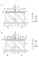
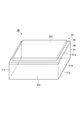
- FIG. It is a fragmentary sectional view of the processing target object shown in FIG. It is a fragmentary sectional view which shows the main processes of the workpiece cutting method which concerns on one Embodiment of this invention. It is a fragmentary sectional view which shows the main processes of the workpiece cutting method which concerns on one Embodiment of this invention. It is a fragmentary sectional view which shows the main processes of the workpiece cutting method which concerns on one Embodiment of this invention. It is a perspective view of the light emitting element obtained by the processing object cutting method concerning one embodiment of the present invention.
- the modified region is formed inside the processing object along the planned cutting line by irradiating the processing target with laser light along the planned cutting line. Form. First, the formation of the modified region will be described with reference to FIGS.
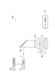
- a laser processing apparatus 100 includes a laser light source 101 that oscillates a laser beam L, a dichroic mirror 103 that is arranged to change the direction of the optical axis (optical path) of the laser beam L by 90 °, and And a condensing lens 105 for condensing the laser light L. Further, the laser processing apparatus 100 includes a support base 107 for supporting the workpiece 1 irradiated with the laser light L condensed by the condensing lens 105, and a stage 111 for moving the support base 107. In addition, a laser light source control unit 102 that controls the laser light source 101 and a stage control unit 115 that controls the movement of the stage 111 are provided to adjust the output, pulse width, and the like of the laser light L.
- the laser light L emitted from the laser light source 101 has its optical axis changed by 90 ° by the dichroic mirror 103, and the inside of the processing object 1 placed on the support base 107.
- the light is condensed by the condensing lens 105.
- the stage 111 is moved, and the workpiece 1 is moved relative to the laser beam L along the planned cutting line 5. As a result, a modified region along the planned cutting line 5 is formed on the workpiece 1.
- a scheduled cutting line 5 for cutting the workpiece 1 is set in the workpiece 1.
- the planned cutting line 5 is a virtual line extending linearly.
- the modified region is formed inside the workpiece 1, as shown in FIG. 3, the laser light L is cut along the planned cutting line 5 in a state where the focused point P is aligned with the inside of the workpiece 1. (Ie, in the direction of arrow A in FIG. 2).
- the modified region 7 is formed inside the workpiece 1 along the planned cutting line 5, and the modified region 7 formed along the planned cutting line 5. Becomes the cutting start region 8.
- the condensing point P is a location where the laser light L is condensed.
- the planned cutting line 5 is not limited to a straight line, but may be a curved line, or may be a line actually drawn on the surface 3 of the workpiece 1 without being limited to a virtual line.
- the modified region 7 may be formed continuously or intermittently. Further, the modified region 7 may be in the form of a line or a dot. In short, the modified region 7 only needs to be formed at least inside the workpiece 1.
- a crack may be formed starting from the modified region 7, and the crack and modified region 7 may be exposed on the outer surface (front surface, back surface, or outer peripheral surface) of the workpiece 1.
- the laser light L here passes through the workpiece 1 and is particularly absorbed near the condensing point inside the workpiece 1, thereby forming the modified region 7 in the workpiece 1. (Ie, internal absorption laser processing). Therefore, since the laser beam L is hardly absorbed by the surface 3 of the workpiece 1, the surface 3 of the workpiece 1 is not melted. In general, when a removed portion such as a hole or a groove is formed by being melted and removed from the front surface 3 (surface absorption laser processing), the processing region gradually proceeds from the front surface 3 side to the back surface side.
- the modified region formed in the present embodiment refers to a region in which density, refractive index, mechanical strength, and other physical characteristics are different from the surroundings.
- the modified region include a melt treatment region, a crack region, a dielectric breakdown region, a refractive index change region, and the like, and there is a region where these are mixed.
- the modified region there may be a region in which the density of the modified region is changed in comparison with the density of the non-modified region in the material to be processed, or lattice defects may be formed (collectively, these are highly dense. Also known as the metastatic region).
- the area where the density of the melt treatment area, the refractive index change area, the modified area has changed compared to the density of the non-modified area, and the area where lattice defects are formed are further included in these areas and the modified areas.
- cracks are included in the interface between the non-modified region and the non-modified region.
- the included crack may be formed over the entire surface of the modified region, or may be formed in only a part or a plurality of parts.
- the modified region 7 is formed by forming a plurality of modified spots (processing marks) along the planned cutting line 5.
- the modified spot is a modified portion formed by one pulse shot of pulsed laser light (that is, one pulse of laser irradiation: laser shot).
- Examples of the modified spot include a crack spot, a melting treatment spot, a refractive index change spot, or a mixture of at least two of these.
- the size of the modified spot and the length of the crack to be generated are appropriately determined. It is preferable to control.
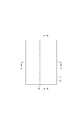
- FIG. 7 is a plan view of a processing object to which the processing object cutting method according to the present embodiment is applied.
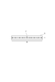
- FIG. 8 is a diagram showing a crystal structure of a material constituting the substrate of the object to be processed shown in FIG.
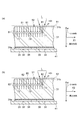
- FIG. 9 is a partial cross-sectional view of the workpiece shown in FIG. 9A is a cross-sectional view taken along the axis x1 in FIG. 7, and
- FIG. 9B is a cross-sectional view taken along the axis x2 in FIG.
- the workpiece 1 is a wafer including a substrate 31 having a disk shape (for example, 2 to 6 inches in diameter and 50 to 200 ⁇ m in thickness).
- the substrate 31 is made of a hexagonal compound (here, single crystal sapphire) having a hexagonal crystal structure.
- the c-axis of the hexagonal compound is inclined by an angle ⁇ (for example, 0.1 °) with respect to the thickness direction of the substrate 31. That is, the substrate 31 has an off angle of the angle ⁇ . More specifically, the substrate 31 has a front surface 31a and a back surface 31b that form an angle ⁇ corresponding to the off-angle with the c-plane of the hexagonal compound.
- the m-plane of the hexagonal compound is inclined by an angle ⁇ with respect to the thickness direction of the substrate 31, and the a-plane of the hexagonal compound is parallel to the thickness direction of the substrate 31. ing.
- the workpiece 1 has a plurality of light emitting element portions (semiconductor element portions) 32 formed on the surface 31 a of the substrate 31.
- the light emitting element portions 32 are arranged in a matrix on the surface 31a of the substrate 31 along the direction of the axis x1 (first direction) and the direction of the axis x2 (second direction).
- the axis x1 is an axis parallel to the front surface 31a and the back surface 31b of the substrate 31 and along the direction intersecting the a-plane and the m-plane of the hexagonal compound.
- the intersection angle ⁇ between the a-plane of the hexagonal compound and the axis x1 is, for example, about 45 °.
- the axis x2 is an axis parallel to the front surface 31a and the back surface 31b of the substrate 31 and along a direction substantially orthogonal to the direction of the axis x1. Therefore, the axis x2 is also parallel to the front surface 31a and the back surface 31b of the substrate 31 and intersects the a-plane and m-plane of the hexagonal compound.
- the intersection angle ⁇ between the m-plane of the hexagonal compound and the axis x2 is, for example, about 45 °.
- the light emitting element portion 32 is arranged along the directions of the axes x1 and x2 rotated about 45 ° from the a-plane and the m-plane of the hexagonal compound along the front surface 31a and the back surface 31b of the substrate 31, respectively. Has been.
- the arrangement direction of the light emitting element portions 32 is not parallel (not along) either the a-plane or the m-plane of the hexagonal compound.
- the workpiece 1 is provided with an orientation flat OF so as to be parallel to the a-plane of the hexagonal compound. Therefore, the light emitting element portion 32 is arranged in a direction that is not parallel (not along) the orientation flat.
- the light emitting element sections 32 arranged in this way are composed of a semiconductor layer 34 stacked on the surface 31 a of the substrate 31, and a semiconductor layer 35 stacked on the semiconductor layer 34.
- the semiconductor layer 34 has a first conductivity type (for example, n-type).
- the semiconductor layer 34 is continuously formed over all the light emitting element portions 32.
- the semiconductor layer 35 has a second conductivity type (for example, p-type) different from the first conductivity type.
- the semiconductor layer 35 is separated for each light emitting element portion 32 and formed in an island shape.
- the semiconductor layers 34 and 35 are made of a III-V group compound semiconductor such as GaN, for example, and form a pn junction with each other.
- a plurality of cuts are made along the direction of the axis x1 so as to pass between the adjacent light emitting element portions 32 and 32 (more specifically, between the adjacent semiconductor layers 35 and 35).
- a planned line (first cut planned line) 51 is set, and a plurality of planned cut lines (second cut planned lines) 52 are set along the direction of the axis x2.
- the planned cutting lines 51 and 52 extend in directions that are not parallel to (or do not follow) the a-plane and m-plane of the hexagonal compound, respectively.
- a processing target cutting method for manufacturing the plurality of light emitting elements (semiconductor elements) by cutting the processing target 1 configured as described above for each light emitting element portion 32 will be described.
- this processing object cutting method first, the processing object 1 described above is prepared (first step). And after affixing the protective tape 41 so that the light emitting element part 32 may be covered with respect to the prepared workpiece 1, it processes on the support stand 107 of the laser processing apparatus 100 mentioned above via the protective tape 41. FIG. The object 1 is placed (see FIGS. 1 and 10).
- the rear surface 31 b of the substrate 31 is set as the incident surface of the laser beam L on the substrate 31, and the condensing point P of the laser beam L is aligned in the substrate 31 to be cut.
- the condensing point P is relatively moved along each of the lines 51.
- a modified region (first modified region) 71 is formed in the substrate 31 along each of the planned cutting lines 51 (that is, along the axis x1 intersecting the a-plane and the m-plane), and the modification is performed.
- a crack (first crack) 81 generated from the mass region 71 is made to reach the back surface 31b of the substrate 31 (second step). At this time, the crack 81 does not reach the surface 31 a of the substrate 31 but extends from the modified region 71 to the surface 31 a side.
- the rear surface 31 b of the substrate 31 is set as the incident surface of the laser beam L on the substrate 31, and the condensing point P of the laser beam L is aligned in the substrate 31 to be cut.
- the condensing point P is relatively moved along each of the lines 52.
- a modified region (second modified region) 72 is formed in the substrate 31 along each of the planned cutting lines 52 (that is, along the axis x2 intersecting the a-plane and the m-plane), and the modification is performed.
- a crack (second crack) 82 generated from the quality region 72 is caused to reach the back surface 31b of the substrate 31 (third step). At this time, the crack 82 does not reach the surface 31a of the substrate 31, but extends from the modified region 72 to the surface 31a side.
- the modified regions 71 and 72 are formed in the substrate 31 along the planned cutting lines 51 and 52 that are not parallel to the a-plane and the m-plane of the hexagonal compound, the modified regions 71 and 72 are formed.
- the influence of the crystal structure of the hexagonal compound constituting the substrate 31 can be suppressed.
- the modified regions 71 and 72 formed in the substrate 31 include a melt processing region. Further, the crack 81 generated from the modified region 71 and the crack 82 generated from the modified region 72 can reach the back surface 31b of the substrate 31 by appropriately adjusting the irradiation condition of the laser light L. .
- the irradiation conditions of the laser beam L for causing the cracks 81 and 82 to reach the back surface 31b include, for example, the distance from the back surface 31b to the position where the condensing point P of the laser beam L is aligned, the pulse width of the laser beam L, and the laser beam L pulse pitch (a value obtained by dividing “the moving speed of the condensing point P of the laser beam L relative to the workpiece 1” by “the repetition frequency of the laser beam L”), the pulse energy of the laser beam L, and the like.
- the method for cutting the workpiece will be explained.
- the modified areas 71 and 72 formed in the above process are used as starting points, respectively.
- the workpiece 1 is cut for each of the light emitting element portions 32 (fourth step). More specifically, in this step, first, as shown in FIG. 11, after the expanded tape 42 is attached to the workpiece 1 so as to cover the back surface 31 b of the substrate 31, The workpiece 1 is placed on the receiving member 43 via the expanded tape 42.
- the knife edge 44 is pressed against the workpiece 1 through the protective tape 41 from the surface 31 a side of the substrate 31 along each of the scheduled cutting lines 51.
- an external force is applied to the workpiece 1 along each of the scheduled cutting lines 51.
- the crack 81 generated from the modified region 71 is extended to the surface 31 a side of the substrate 31, and the workpiece 1 is cut into a bar shape along each of the scheduled cutting lines 51.
- the knife edge 44 is pressed against the workpiece 1 through the protective tape 41 from the surface 31 a side of the substrate 31 along each of the scheduled cutting lines 52.
- an external force is applied to the workpiece 1 along each of the scheduled cutting lines 52.
- the crack 82 generated from the modified region 72 is extended to the surface 31 a side of the substrate 31, and the workpiece 1 is cut into chips along each of the scheduled cutting lines 52.
- the protective tape 41 is removed from the workpiece 1 and the expanded tape 42 is expanded outward as shown in FIG.
- the plurality of light emitting elements (semiconductor elements) 10 obtained by cutting the workpiece 1 into chips are separated from each other.
- the light emitting device 10 obtained in this way has a substantially rectangular parallelepiped shape as shown in FIG.
- the light-emitting element 10 is made of a hexagonal compound (here, single crystal sapphire), and has a base 31 (substrate 31) having a front surface 31a and a back surface 31b that form an angle ⁇ corresponding to the c-plane of the hexagonal compound and an off-angle. And a light emitting element portion 32 formed on the surface 31a of the base portion.
- the base 31 has a pair of side surfaces (first side surfaces) 31c facing each other while connecting the front surface 31a and the back surface 31b, and a pair of side surfaces (first surfaces) orthogonal to the side surface 31c while connecting the front surface 31a and the back surface 31b. 2 side) 32c.
- the side surface 31c is a cut surface formed when the workpiece 1 is cut along the planned cutting line 51, for example.
- the side surface 32c is a cut surface formed when the workpiece 1 is cut along the planned cutting line 52, for example.
- the side surfaces 31c and 32c of the base portion 31 extend in directions intersecting with the a-plane and m-plane of the hexagonal compound constituting the base portion 31 (that is, not parallel to the a-plane and m-plane).
- the processing object 1 is prepared.
- the workpiece 1 prepared here is made of a hexagonal compound, and is formed on a substrate 31 having a surface 31a and a back surface 31b that form an angle ⁇ corresponding to the c-plane and an off-angle, and the surface 31a of the substrate 31.
- a plurality of light emitting element portions 32 are parallel to the front surface 31a and the back surface 31b of the substrate 31, and is parallel to the direction of the axis x1 intersecting the a plane and the m plane of the hexagonal compound, and the front surface 31a and the back surface 31b of the substrate 31. And arranged in a matrix along the direction of the axis x2 orthogonal to the axis x1.
- the planned cutting line 51 and the planned cutting line 52 for cutting the workpiece 1 are set along the directions of the axes x1 and x2 so as to pass between the adjacent light emitting element portions 32 and 32, respectively. Is done. That is, in this processing object cutting method, the planned cutting lines 51 and 52 are set so as not to be parallel to the a-plane and the m-plane of the hexagonal compound.
- the modified regions 71 and 72 are formed by irradiating the laser beam L along the scheduled cutting lines 51 and 52, and the modified regions 71 and 72 are formed. The processing object 1 is cut from the starting point.
- each light emitting element portion 32 The light emitting element 10 can be manufactured by cutting the workpiece 1.
- disconnecting the said processing object 1 are each on the a surface and m surface of a hexagonal system compound as mentioned above. It can be set not to be parallel. Then, the modified regions 71 and 72 are formed by irradiating the laser beam L along the scheduled cutting lines 51 and 52 set as described above, and the workpiece 1 is cut using the modified regions 71 and 72 as starting points. By doing so, it is possible to manufacture the semiconductor element 10 by cutting the workpiece 1 while suppressing the influence of the crystal structure of the hexagonal compound constituting the substrate 31.
- processing object cutting method the processing object, and the semiconductor element according to the present invention. Therefore, the processing object cutting method, the processing object, and the semiconductor element according to the present invention are not limited to those described above.
- the processing object cutting method, the processing object, and the semiconductor element according to the present invention can be arbitrarily modified from the above-described ones within the scope not changing the gist of each claim.
- the material composing the substrate 31 of the workpiece 1 is not limited to single crystal sapphire, and any hexagonal crystal such as gallium nitride (eg GaN) or silicon carbide (eg SiC) having a hexagonal crystal structure. System compounds.
- the crossing angles ⁇ , ⁇ of the axes x1 and x2 that is, the planned cutting line 51 and the planned cutting line 52
- orientation flat OF in the workpiece 1 is not limited to those parallel to the a-plane of the hexagonal compound constituting the substrate 31 of the workpiece 1.
- the a-plane and the m-plane of the hexagonal compound are included.
- the workpiece 1 may have a semiconductor element portion for an arbitrary functional element instead of the light emitting element portion 32.
- the present invention it is possible to provide a processing object cutting method, a processing object, and a semiconductor element capable of cutting the processing object while suppressing the influence of the crystal structure of the hexagonal compound.
Landscapes
- Engineering & Computer Science (AREA)
- Physics & Mathematics (AREA)
- Optics & Photonics (AREA)
- Mechanical Engineering (AREA)
- Plasma & Fusion (AREA)
- Chemical & Material Sciences (AREA)
- Chemical Kinetics & Catalysis (AREA)
- General Chemical & Material Sciences (AREA)
- Oil, Petroleum & Natural Gas (AREA)
- Laser Beam Processing (AREA)
- Dicing (AREA)
- Processing Of Stones Or Stones Resemblance Materials (AREA)
Description
本発明は、加工対象物を切断して半導体素子を製造するための加工対象物切断方法、加工対象物、及び、半導体素子に関する。
上記技術分野における従来の加工対象物切断方法として、特許文献1には、ダイシングやスクライビングによってサファイア基板の表面及び裏面に分離溝を形成すると共に、レーザ光の照射によってサファイア基板内に加工変質部を多段的に形成し、分離溝及び加工変質部に沿ってサファイア基板を切断する方法が記載されている。
ところで、上述したサファイア等の六方晶系化合物からなり、その六方晶系化合物のc面とオフ角分の角度を成す表面及び裏面を有する基板を備える加工対象物を切断するために、基板の表裏面と六方晶系化合物のa面とに平行な切断予定ライン、及び、基板の表裏面と六方晶系化合物のm面とに平行な切断予定ラインを加工対象物に設定する場合がある。そのような場合には、それぞれの切断予定ラインに沿ってレーザ光を照射することにより基板内に形成された改質領域を起点として加工対象物を切断すると、六方晶系化合物の結晶構造がその切断に影響を及ぼす場合がある。
本発明は、そのような事情に鑑みてなされたものであり、六方晶系化合物の結晶構造の影響を抑制しつつ加工対象物を切断可能な加工対象物切断方法、加工対象物、及び半導体素子を提供することを課題とする。
本発明の一側面は、加工対象物切断方法に関する。この加工対象物切断方法は、六方晶系化合物からなり六方晶系化合物のc面とオフ角分の角度をなす表面及び裏面を有する基板と、基板の表面上に形成され第1及び第2方向に沿ってマトリックス状に配列された複数の半導体素子部とを有する加工対象物を用意する第1工程と、基板内にレーザ光の集光点を合わせ、隣り合う半導体素子部の間を通るように第1方向に沿って設定された複数の第1切断予定ラインのそれぞれに沿って集光点を相対的に移動させることにより、第1切断予定ラインのそれぞれに沿って基板内に第1改質領域を形成する第2工程と、基板内にレーザ光の集光点を合わせ、隣り合う半導体素子部の間を通るように第2方向に沿って設定された複数の第2切断予定ラインのそれぞれに沿って集光点を相対的に移動させることにより、第2切断予定ラインのそれぞれに沿って基板内に第2改質領域を形成する第3工程と、第1及び第2切断予定ラインのそれぞれに沿って加工対象物に外力を作用させることにより、第1及び第2改質領域を起点として、第1及び第2切断予定ラインのそれぞれに沿って加工対象物を切断し、半導体素子部を含む半導体素子を製造する第4工程と、を備え、第1方向は、基板の表面及び裏面に平行であり、且つ、六方晶系化合物のa面及びm面に交差する方向であり、第2方向は、基板の表面及び裏面に平行であり、且つ、第1方向に直交する方向である、ことを特徴とする。
この加工対象物切断方法においては、まず、加工対象物を用意する。ここで用意する加工対象物は、六方晶系化合物からなり、そのc面とオフ角分の角度をなす表裏面を有する基板と、基板の表面上に形成された複数の半導体素子部とを有している。半導体素子部は、基板の表裏面に平行であり、且つ、六方晶系化合物のa面及びm面に交差する第1方向と、基板の表裏面に平行であり、且つ、第1方向に直交する第2方向とに沿ってマトリックス状に配列されている。そして、当該加工対象物を切断するための切断予定ラインが、隣り合う半導体素子部の間を通るように第1方向及び第2方向に沿って設定される。つまり、切断予定ラインが、六方晶系化合物のa面及びm面のそれぞれに平行にならないように設定される。そして、この加工対象物切断方法においては、そのように設定される切断予定ラインに沿ってレーザ光を照射して改質領域を形成し、その改質領域を起点として加工対象物を切断する。このため、この加工対象物切断方法によれば、基板を構成する六方晶系化合物の結晶構造の影響を抑制しつつ、加工対象物を切断して半導体素子を製造することができる。なお、オフ角は0°の場合を含む。その場合には、基板の表裏面は、六方晶系化合物のc面に平行となる。
本発明の一側面に係る加工対象物切断方法においては、第2工程において、基板の裏面をレーザ光の入射面とすると共に、第1改質領域から発生した第1亀裂を基板の裏面に到達させ、第3工程において、基板の裏面をレーザ光の入射面とすると共に、第2改質領域から発生した第2亀裂を基板の裏面に到達させ、第4工程においては、加工対象物に外力を作用させることにより、第1及び第2亀裂を伸展させて加工対象物を切断することができる。この場合、基板の内部に改質領域を形成する際に、半導体素子部へのレーザ光の影響を抑制することができる。
ここで、本発明の他の側面は、加工対象物に関する。この加工対象物は、六方晶系化合物からなり六方晶系化合物のc面とオフ角分の角度をなす表面及び裏面を有する基板と、基板の表面上に形成された複数の半導体素子部とを有する加工対象物であって、複数の半導体素子部は、基板の表面及び裏面に平行であり、且つ、六方晶系化合物のa面及びm面に交差する第1方向と、基板の表面及び裏面に平行であり、且つ、第1方向に直交する第2方向とに沿ってマトリックス状に配列されている、ことを特徴とする。
この加工対象物においては、当該加工対象物を切断するための切断予定ラインを、上述したように、六方晶系化合物のa面及びm面のそれぞれに平行にならないように設定することができる。そして、そのように設定された切断予定ラインに沿ってレーザ光を照射して改質領域を形成し、その改質領域を起点として加工対象物を切断すれば、基板を構成する六方晶系化合物の結晶構造の影響を抑制しつつ切断して半導体素子を製造することが可能となる。
また、本発明のさらに他の側面は、半導体素子に関する。この半導体素子は、六方晶系化合物からなり六方晶系化合物のc面とオフ角分の角度をなす表面及び裏面を有する基部と、基部の表面上に形成された半導体素子部とを有する半導体素子であって、基部は、表面と裏面とを接続しつつ互いに対向する一対の第1側面と、表面と裏面とを接続しつつ第1側面に直交する一対の第2側面とを有し、第1の側面のそれぞれは、六方晶系化合物のa面及びm面に交差している、ことを特徴とする。この場合、基部を構成する六方晶系化合物の結晶構造が素子特性に影響を及ぼすことを抑制することができる。
ここで、上述した六方晶系化合物は単結晶サファイアとすることができ、半導体素子部は光を発生するための発光素子部とすることができる。
本発明によれば、六方晶系化合物の結晶構造の影響を抑制しつつ加工対象物を切断可能な加工対象物切断方法、加工対象物、及び半導体素子を提供することができる。
以下、本発明の一実施形態について、図面を参照して詳細に説明する。なお、各図において、同一又は相当部分には同一の符号を付し、重複する説明を省略する。
本発明の一実施形態に係る加工対象物切断方法においては、切断予定ラインに沿って加工対象物にレーザ光を照射することにより、切断予定ラインに沿って加工対象物の内部に改質領域を形成する。そこで、まず、この改質領域の形成について、図1~図6を参照して説明する。
図1に示されるように、レーザ加工装置100は、レーザ光Lをパルス発振するレーザ光源101と、レーザ光Lの光軸(光路)の向きを90°変えるように配置されたダイクロイックミラー103と、レーザ光Lを集光するための集光用レンズ105とを備えている。また、レーザ加工装置100は、集光用レンズ105で集光されたレーザ光Lが照射される加工対象物1を支持するための支持台107と、支持台107を移動させるためのステージ111と、レーザ光Lの出力やパルス幅等を調節するためにレーザ光源101を制御するレーザ光源制御部102と、ステージ111の移動を制御するステージ制御部115とを備えている。
このレーザ加工装置100においては、レーザ光源101から出射されたレーザ光Lは、ダイクロイックミラー103によってその光軸の向きを90°変えられ、支持台107上に載置された加工対象物1の内部に集光用レンズ105によって集光される。これと共に、ステージ111が移動させられ、加工対象物1がレーザ光Lに対して切断予定ライン5に沿って相対移動させられる。これにより、切断予定ライン5に沿った改質領域が加工対象物1に形成されることとなる。
図2に示されるように、加工対象物1には、加工対象物1を切断するための切断予定ライン5が設定されている。切断予定ライン5は、直線状に延びた仮想線である。加工対象物1の内部に改質領域を形成する場合、図3に示されるように、加工対象物1の内部に集光点Pを合わせた状態で、レーザ光Lを切断予定ライン5に沿って(すなわち、図2の矢印A方向に)相対的に移動させる。これにより、図4~図6に示されるように、改質領域7が切断予定ライン5に沿って加工対象物1の内部に形成され、切断予定ライン5に沿って形成された改質領域7が切断起点領域8となる。
なお、集光点Pとは、レーザ光Lが集光する箇所のことである。また、切断予定ライン5は、直線状に限らず曲線状であってもよいし、仮想線に限らず加工対象物1の表面3に実際に引かれた線であってもよい。また、改質領域7は、連続的に形成される場合もあるし、断続的に形成される場合もある。また、改質領域7は、列状でも点状でもよく、要は、改質領域7は少なくとも加工対象物1の内部に形成されていればよい。また、改質領域7を起点に亀裂が形成される場合があり、亀裂及び改質領域7は、加工対象物1の外表面(表面、裏面、若しくは外周面)に露出していてもよい。
ちなみに、ここでのレーザ光Lは、加工対象物1を透過すると共に加工対象物1の内部の集光点近傍にて特に吸収され、これにより、加工対象物1に改質領域7が形成される(すなわち、内部吸収型レーザ加工)。よって、加工対象物1の表面3ではレーザ光Lが殆ど吸収されないので、加工対象物1の表面3が溶融することはない。一般的に、表面3から溶融され除去されて穴や溝等の除去部が形成される(表面吸収型レーザ加工)場合、加工領域は表面3側から徐々に裏面側に進行する。
ところで、本実施形態で形成される改質領域は、密度、屈折率、機械的強度やその他の物理的特性が周囲とは異なる状態になった領域をいう。改質領域としては、例えば、溶融処理領域、クラック領域、絶縁破壊領域、屈折率変化領域等があり、これらが混在した領域もある。更に、改質領域としては、加工対象物の材料において改質領域の密度が非改質領域の密度と比較して変化した領域や、格子欠陥が形成された場合がある(これらをまとめて高密転移領域ともいう)。
また、溶融処理領域や屈折率変化領域、改質領域の密度が非改質領域の密度と比較して変化した領域、格子欠陥が形成された領域は、更に、それら領域の内部や改質領域と非改質領域との界面に亀裂(割れ、マイクロクラック)を内包している場合がある。内包される亀裂は改質領域の全面に渡る場合や一部分のみや複数部分に形成される場合がある。
また、本実施形態においては、切断予定ライン5に沿って改質スポット(加工痕)を複数形成することによって、改質領域7を形成している。改質スポットとは、パルスレーザ光の1パルスのショット(つまり1パルスのレーザ照射:レーザショット)で形成される改質部分であり、改質スポットが集まることにより改質領域7となる。改質スポットとしては、クラックスポット、溶融処理スポット、若しくは屈折率変化スポット、又はこれらの少なくとも2つが混在するもの等が挙げられる。
この改質スポットについては、要求される切断精度、要求される切断面の平坦性、加工対象物の厚さ、種類、結晶方位等を考慮して、その大きさや発生する亀裂の長さを適宜制御することが好ましい。
引き続いて、本発明の一実施形態に係る加工対象物切断方法について説明する。図7は、本実施形態に係る加工対象物切断方法が適用される加工対象物の平面図である。図8は、図7に示された加工対象物の基板を構成する材料の結晶構造を示す図である。図9は、図7に示された加工対象物の部分断面図である。特に、図9の(a)は、図7の軸x1に沿った断面図であり、図9の(b)は、図7の軸x2に沿った断面図である。図7~9に示されるように、加工対象物1は、円板形状(例えば、直径2~6インチ、厚さ50~200μm)の基板31を備えるウェハである。
基板31は、六方晶系の結晶構造を有する六方晶系化合物(ここでは単結晶サファイア)からなる。基板31において、六方晶系化合物のc軸は、基板31の厚さ方向に対して角度θ(例えば0.1°)だけ傾斜している。つまり、基板31は、角度θのオフ角を有している。より具体的には、基板31は、六方晶系化合物のc面とオフ角分の角度θをなす表面31a及び裏面31bを有している。基板31においては、六方晶系化合物のm面は、基板31の厚さ方向に対して角度θだけ傾斜しており、六方晶系化合物のa面は、基板31の厚さ方向に平行となっている。
加工対象物1は、基板31の表面31aの上に形成された複数の発光素子部(半導体素子部)32を有している。発光素子部32は、基板31の表面31aの上において、軸x1の方向(第1方向)と軸x2の方向(第2方向)とに沿ってマトリックス状に配列されている。軸x1は、基板31の表面31a及び裏面31bに平行であり、且つ、六方晶系化合物のa面及びm面に交差する方向に沿った軸である。六方晶系化合物のa面と軸x1との交差角度φは例えば45°程度である。
軸x2は、基板31の表面31a及び裏面31bに平行であり、且つ、軸x1の方向に略直交する方向に沿った軸である。したがって、軸x2も、基板31の表面31a及び裏面31bに平行であり、且つ、六方晶系化合物のa面及びm面に交差する。六方晶系化合物のm面と軸x2との交差角度ψは例えば45°程度である。つまり、発光素子部32は、基板31の表面31a及び裏面31bに沿って、六方晶系化合物のa面及びm面のそれぞれから45°程度回転させた軸x1及び軸x2の方向に沿って配列されている。
したがって、発光素子部32の配列方向は、六方晶系化合物のa面及びm面のいずれにも平行でない(沿っていない)。また、加工対象物1には、六方晶系化合物のa面に平行となるようにオリエンテーションフラットOFが設けられている。よって、発光素子部32は、このオリエンテーションフラットに対しても平行でない(沿っていない)方向に配列されることとなる。
このようにして配列された発光素子部32は、図9に示されるように、基板31の表面31aの上に積層された半導体層34と、半導体層34の上に積層された半導体層35とを有している。半導体層34は、第1導電型(例えばn型)を有する。半導体層34は、全ての発光素子部32にわたって一続きに形成されている。半導体層35は、第1導電型と異なる第2導電型(例えばp型)を有する。半導体層35は、発光素子部32ごとに分離されてアイランド状に形成されている。半導体層34,35は、例えばGaN等のIII-V族化合物半導体からなり、互いにpn接合をなしている。
そして、加工対象物1においては、隣り合う発光素子部32,32の間(より具体的には隣り合う半導体層35,35の間)を通るように、軸x1の方向に沿って複数の切断予定ライン(第1切断予定ライン)51が設定されており、軸x2の方向に沿って複数の切断予定ライン(第2切断予定ライン)52が設定されている。切断予定ライン51,52は、それぞれ、六方晶系化合物のa面及びm面に平行でない(沿わない)方向に延在している。
引き続いて、以上のように構成された加工対象物1を発光素子部32ごとに切断して複数の発光素子(半導体素子)を製造するための加工対象物切断方法について説明する。この加工対象物切断方法においては、まず、上述した加工対象物1を用意する(第1工程)。そして、用意した加工対象物1に対して、発光素子部32を覆うように保護テープ41を貼り付けた後に、上述したレーザ加工装置100の支持台107の上に、保護テープ41を介して加工対象物1を載置する(図1,10参照)。
続いて、図10の(a)に示されるように、基板31の裏面31bを基板31におけるレーザ光Lの入射面として、基板31内にレーザ光Lの集光点Pを合わせて、切断予定ライン51のそれぞれに沿って集光点Pを相対的に移動させる。これにより、切断予定ライン51のそれぞれに沿って(すなわち、a面及びm面に交差する軸x1に沿って)基板31内に改質領域(第1改質領域)71を形成すると共に、改質領域71から発生した亀裂(第1亀裂)81を基板31の裏面31bに到達させる(第2工程)。このとき、亀裂81は、基板31の表面31aには到達しないものの、改質領域71から表面31a側にも伸展する。
続いて、図10の(b)に示されるように、基板31の裏面31bを基板31におけるレーザ光Lの入射面として、基板31内にレーザ光Lの集光点Pを合わせて、切断予定ライン52のそれぞれに沿って集光点Pを相対的に移動させる。これにより、切断予定ライン52のそれぞれに沿って(すなわち、a面及びm面に交差する軸x2に沿って)基板31内に改質領域(第2改質領域)72を形成すると共に、改質領域72から発生した亀裂(第2亀裂)82を基板31の裏面31bに到達させる(第3工程)。このとき、亀裂82は、基板31の表面31aには到達しないものの、改質領域72から表面31a側にも伸展する。
このように、六方晶系化合物のa面及びm面に平行でない切断予定ライン51,52に沿って、基板31の内部に改質領域71,72を形成すれば、その改質領域71,72を起点とした加工対象物1の切断において、基板31を構成する六方晶系化合物の結晶構造の影響(特に六方晶系化合物のr面の影響)を抑制することができる。
なお、基板31内に形成される改質領域71,72は、溶融処理領域を含むものとなる。また、改質領域71から発生した亀裂81、及び改質領域72から発生した亀裂82は、レーザ光Lの照射条件を適宜調整することによって、基板31の裏面31bに到達させることが可能である。亀裂81,82を裏面31bに到達させるためのレーザ光Lの照射条件としては、例えば、裏面31bからレーザ光Lの集光点Pを合わせる位置までの距離、レーザ光Lのパルス幅、レーザ光Lのパルスピッチ(「加工対象物1に対するレーザ光Lの集光点Pの移動速度」を「レーザ光Lの繰り返し周波数」で除した値)、レーザ光Lのパルスエネルギー等がある。
引き続き加工対象物切断方法について説明する。続く工程では、切断予定ライン51,52のそれぞれに沿って加工対象物1に外力を作用させることにより、上記工程で形成した改質領域71,72を起点として、切断予定ライン51,52のそれぞれに沿って発光素子部32ごとに加工対象物1を切断する(第4工程)。より具体的には、この工程においては、まず、図11に示されるように、基板31の裏面31bを覆うように加工対象物1にエキスパンドテープ42を貼り付けた後に、三点曲げブレーク装置の受け部材43の上に、当該エキスパンドテープ42を介して加工対象物1を載置する。
そして、図11の(a)に示されるように、切断予定ライン51のそれぞれに沿って、基板31の表面31a側から、保護テープ41を介して加工対象物1にナイフエッジ44を押し当てることにより、切断予定ライン51のそれぞれに沿って加工対象物1に外力を作用させる。これにより、改質領域71から発生した亀裂81を基板31の表面31a側に伸展させて、切断予定ライン51のそれぞれに沿って加工対象物1をバー状に切断する。
続いて、図11の(b)に示されるように、切断予定ライン52のそれぞれに沿って、基板31の表面31a側から、保護テープ41を介して加工対象物1にナイフエッジ44を押し当てることにより、切断予定ライン52のそれぞれに沿って加工対象物1に外力を作用させる。これにより、改質領域72から発生した亀裂82を基板31の表面31a側に伸展させて、切断予定ライン52のそれぞれに沿って加工対象物1をチップ状に切断する。
続く工程では、加工対象物1を切断した後、図12に示されるように、加工対象物1から保護テープ41を取り除き、エキスパンドテープ42を外側に拡張させる。これにより、加工対象物1がチップ状に切断させることで得られた複数の発光素子(半導体素子)10を互いに離間させる。
このようにして得られた発光素子10は、図13に示されるように、略直方体状を呈している。また、発光素子10は、六方晶系化合物(ここでは単結晶サファイア)からなり、六方晶系化合物のc面とオフ角分の角度θをなす表面31a及び裏面31bを有する基部31(基板31)と、基部の表面31aの上に形成された発光素子部32とを有している。
そして、基部31は、表面31aと裏面31bとを接続しつつ互いに対向する一対の側面(第1側面)31cと、表面31aと裏面31bとを接続しつつ側面31cに直交する一対の側面(第2側面)32cとを有している。側面31cは、例えば、切断予定ライン51に沿って加工対象物1を切断した際に形成される切断面である。側面32cは、例えば、切断予定ライン52に沿って加工対象物1を切断した際に形成される切断面である。したがって、基部31のそれぞれの側面31c,32cは、基部31を構成する六方晶系化合物のa面及びm面にそれぞれ交差する方向に延びている(すなわち、a面及びm面に平行でない)。
以上説明したように、本実施形態に係る加工対象物切断方法においては、まず、加工対象物1を用意する。ここで用意する加工対象物1は、六方晶系化合物からなり、そのc面とオフ角分の角度θをなす表面31aと裏面31bとを有する基板31と、基板31の表面31a上に形成された複数の発光素子部32とを有している。発光素子部32は、基板31の表面31a及び裏面31bに平行であり、且つ、六方晶系化合物のa面及びm面に交差する軸x1の方向と、基板31の表面31a及び裏面31bに平行であり、且つ、軸x1に直交する軸x2の方向とに沿ってマトリックス状に配列されている。
そして、当該加工対象物1を切断するための切断予定ライン51及び切断予定ライン52が、それぞれ、隣り合う発光素子部32,32の間を通るように軸x1及び軸x2の方向に沿って設定される。つまり、この加工対象物切断方法においては、切断予定ライン51,52が、六方晶系化合物のa面及びm面のそれぞれに平行にならないように設定される。そして、この加工対象物切断方法においては、そのように設定される切断予定ライン51,52に沿ってレーザ光Lを照射して改質領域71,72を形成し、その改質領域71,72を起点として加工対象物1を切断する。このため、この加工対象物切断方法によれば、基板31を構成する六方晶系化合物の結晶構造の影響(特に六方晶系化合物のr面の影響)を抑制しつつ、発光素子部32ごとに加工対象物1を切断して発光素子10を製造することができる。
また、本実施形態に係る加工対象物1においては、当該加工対象物1を切断するための切断予定ライン51,52を、上述したように、六方晶系化合物のa面及びm面のそれぞれに平行にならないように設定することができる。そして、そのように設定された切断予定ライン51,52に沿ってレーザ光Lを照射して改質領域71,72を形成し、その改質領域71,72を起点として加工対象物1を切断すれば、基板31を構成する六方晶系化合物の結晶構造の影響を抑制しつつ加工対象物1を切断して半導体素子10を製造することが可能となる。
以上の実施形態は、本発明に係る加工対象物切断方法、加工対象物、及び、半導体素子の一実施形態を説明したものである。したがって、本発明に係る加工対象物切断方法、加工対象物、及び、半導体素子は、上述したものに限定されない。本発明に係る加工対象物切断方法、加工対象物、及び、半導体素子は、各請求項の要旨を変更しない範囲において、上述したものを任意に変形したものとすることができる。
例えば、加工対象物1の基板31を構成する材料は、単結晶サファイアに限定されず、六方晶系の結晶構造を有する窒化ガリウム(例えばGaN)や炭化ケイ素(例えばSiC)等の任意の六方晶系化合物とすることができる。
また、加工対象物1の基板31を構成する六方晶系化合物のa面及びm面のそれぞれに対する軸x1及び軸x2(すなわち切断予定ライン51及び切断予定ライン52)のそれぞれの交差角度φ,ψは、45°に限定されず、30°(-30°)や60°(-60°)とすることができる。
また、加工対象物1におけるオリエンテーションフラットOFは、加工対象物1の基板31を構成する六方晶系化合物のa面に平行なものに限定されず、例えば、六方晶系化合物のa面及びm面に交差する軸x1や軸x2に平行に形成することができる。
さらに、加工対象物1は、発光素子部32に代えて、任意の機能素子のための半導体素子部を有するものとすることができる。
本発明によれば、六方晶系化合物の結晶構造の影響を抑制しつつ加工対象物を切断可能な加工対象物切断方法、加工対象物、及び半導体素子を提供することができる。
1…加工対象物、10…発光素子(半導体素子)、31…基板(基部)、31a…表面、31b…裏面、31c…側面(第1側面),32c…側面(第2側面)、32…発光素子部(半導体素子部)、51,52…切断予定ライン、71,72…改質領域、81…亀裂(第1亀裂),82…亀裂(第2亀裂)、L…レーザ光、P…集光点、x1…軸(第1方向)、x2…軸(第2方向)。
Claims (6)
- 六方晶系化合物からなり前記六方晶系化合物のc面とオフ角分の角度をなす表面及び裏面を有する基板と、前記基板の前記表面上に形成され第1及び第2方向に沿ってマトリックス状に配列された複数の半導体素子部とを有する加工対象物を用意する第1工程と、
前記基板内にレーザ光の集光点を合わせ、隣り合う前記半導体素子部の間を通るように前記第1方向に沿って設定された複数の第1切断予定ラインのそれぞれに沿って前記集光点を相対的に移動させることにより、前記第1切断予定ラインのそれぞれに沿って前記基板内に第1改質領域を形成する第2工程と、
前記基板内に前記レーザ光の集光点を合わせ、隣り合う前記半導体素子部の間を通るように前記第2方向に沿って設定された複数の第2切断予定ラインのそれぞれに沿って前記集光点を相対的に移動させることにより、前記第2切断予定ラインのそれぞれに沿って前記基板内に第2改質領域を形成する第3工程と、
前記第1及び第2切断予定ラインのそれぞれに沿って前記加工対象物に外力を作用させることにより、前記第1及び第2改質領域を起点として、前記第1及び第2切断予定ラインのそれぞれに沿って前記加工対象物を切断し、前記半導体素子部を含む半導体素子を製造する第4工程と、
を備え、
前記第1方向は、前記基板の前記表面及び前記裏面に平行であり、且つ、前記六方晶系化合物のa面及びm面に交差する方向であり、
前記第2方向は、前記基板の前記表面及び前記裏面に平行であり、且つ、前記第1方向に直交する方向である、
ことを特徴とする加工対象物切断方法。 - 前記第2工程においては、前記基板の前記裏面を前記レーザ光の入射面とすると共に、前記第1改質領域から発生した第1亀裂を前記基板の裏面に到達させ、
前記第3工程においては、前記基板の前記裏面を前記レーザ光の入射面とすると共に、前記第2改質領域から発生した第2亀裂を前記基板の前記裏面に到達させ、
前記第4工程においては、前記加工対象物に外力を作用させることにより、前記第1及び第2亀裂を伸展させて前記加工対象物を切断する、ことを特徴とする請求項1に記載の加工対象物切断方法。 - 前記六方晶系化合物は、単結晶サファイアであり、
前記半導体素子部は、発光素子部である、ことを特徴とする請求項1又は2に記載の加工対象物切断方法。 - 六方晶系化合物からなり前記六方晶系化合物のc面とオフ角分の角度をなす表面及び裏面を有する基板と、前記基板の前記表面上に形成された複数の半導体素子部とを有する加工対象物であって、
複数の前記半導体素子部は、前記基板の前記表面及び前記裏面に平行であり、且つ、前記六方晶系化合物のa面及びm面に交差する第1方向と、前記基板の前記表面及び前記裏面に平行であり、且つ、前記第1方向に直交する第2方向とに沿ってマトリックス状に配列されている、
ことを特徴とする加工対象物。 - 前記六方晶系化合物は、単結晶サファイアであり、
前記半導体素子部は、発光素子部である、ことを特徴とする請求項4に記載の加工対象物。 - 六方晶系化合物からなり前記六方晶系化合物のc面とオフ角分の角度をなす表面及び裏面を有する基部と、前記基部の前記表面上に形成された半導体素子部とを有する半導体素子であって、
前記基部は、前記表面と前記裏面とを接続しつつ互いに対向する一対の第1側面と、前記表面と前記裏面とを接続しつつ前記第1側面に直交する一対の第2側面とを有し、
前記第1の側面のそれぞれは、前記六方晶系化合物のa面及びm面に交差している、
ことを特徴とする半導体素子。
Applications Claiming Priority (2)
| Application Number | Priority Date | Filing Date | Title |
|---|---|---|---|
| JP2012-117805 | 2012-05-23 | ||
| JP2012117805A JP2013247147A (ja) | 2012-05-23 | 2012-05-23 | 加工対象物切断方法、加工対象物、及び、半導体素子 |
Publications (1)
| Publication Number | Publication Date |
|---|---|
| WO2013176089A1 true WO2013176089A1 (ja) | 2013-11-28 |
Family
ID=49623779
Family Applications (1)
| Application Number | Title | Priority Date | Filing Date |
|---|---|---|---|
| PCT/JP2013/063962 Ceased WO2013176089A1 (ja) | 2012-05-23 | 2013-05-20 | 加工対象物切断方法、加工対象物、及び、半導体素子 |
Country Status (3)
| Country | Link |
|---|---|
| JP (1) | JP2013247147A (ja) |
| TW (1) | TW201411706A (ja) |
| WO (1) | WO2013176089A1 (ja) |
Cited By (4)
| Publication number | Priority date | Publication date | Assignee | Title |
|---|---|---|---|---|
| US9142712B2 (en) | 2013-12-02 | 2015-09-22 | Nichia Corporation | Method for manufacturing light emitting element |
| KR20160119718A (ko) * | 2015-04-06 | 2016-10-14 | 가부시기가이샤 디스코 | 웨이퍼의 생성 방법 |
| JP2016197699A (ja) * | 2015-04-06 | 2016-11-24 | 株式会社ディスコ | ウエーハの生成方法 |
| JP2016197698A (ja) * | 2015-04-06 | 2016-11-24 | 株式会社ディスコ | ウエーハの生成方法 |
Families Citing this family (14)
| Publication number | Priority date | Publication date | Assignee | Title |
|---|---|---|---|---|
| JP6217382B2 (ja) * | 2013-12-24 | 2017-10-25 | 豊田合成株式会社 | 基板分割方法 |
| JP2016030364A (ja) * | 2014-07-28 | 2016-03-07 | 三星ダイヤモンド工業株式会社 | 貼り合わせ基板の分断方法及び分断装置 |
| JP2016030413A (ja) * | 2014-07-30 | 2016-03-07 | 三星ダイヤモンド工業株式会社 | 貼り合わせ基板の分断方法及び分断装置 |
| JP2016207908A (ja) * | 2015-04-27 | 2016-12-08 | 三菱電機株式会社 | 炭化珪素半導体装置の製造方法および炭化珪素半導体装置 |
| JP6265175B2 (ja) | 2015-06-30 | 2018-01-24 | 日亜化学工業株式会社 | 半導体素子の製造方法 |
| JP6486239B2 (ja) * | 2015-08-18 | 2019-03-20 | 株式会社ディスコ | ウエーハの加工方法 |
| JP6486240B2 (ja) * | 2015-08-18 | 2019-03-20 | 株式会社ディスコ | ウエーハの加工方法 |
| JP2019009199A (ja) * | 2017-06-22 | 2019-01-17 | 株式会社ディスコ | ウェーハ及びウェーハの加工方法 |
| JP6579397B2 (ja) * | 2017-08-30 | 2019-09-25 | 日亜化学工業株式会社 | 発光素子の製造方法 |
| DE202019005382U1 (de) | 2018-08-10 | 2020-06-17 | Rohm Co., Ltd. | SiC-Halbleitervorrichtung |
| JP6664445B2 (ja) * | 2018-08-10 | 2020-03-13 | ローム株式会社 | SiC半導体装置 |
| JP6563093B1 (ja) * | 2018-08-10 | 2019-08-21 | ローム株式会社 | SiC半導体装置 |
| KR102857400B1 (ko) | 2019-09-30 | 2025-09-10 | 니치아 카가쿠 고교 가부시키가이샤 | 발광 소자의 제조 방법 |
| JP7129436B2 (ja) * | 2020-02-17 | 2022-09-01 | ローム株式会社 | SiC半導体装置 |
Citations (1)
| Publication number | Priority date | Publication date | Assignee | Title |
|---|---|---|---|---|
| JP2011243730A (ja) * | 2010-05-18 | 2011-12-01 | Showa Denko Kk | 半導体発光チップおよび基板の加工方法 |
-
2012
- 2012-05-23 JP JP2012117805A patent/JP2013247147A/ja active Pending
-
2013
- 2013-05-20 WO PCT/JP2013/063962 patent/WO2013176089A1/ja not_active Ceased
- 2013-05-22 TW TW102118038A patent/TW201411706A/zh unknown
Patent Citations (1)
| Publication number | Priority date | Publication date | Assignee | Title |
|---|---|---|---|---|
| JP2011243730A (ja) * | 2010-05-18 | 2011-12-01 | Showa Denko Kk | 半導体発光チップおよび基板の加工方法 |
Cited By (7)
| Publication number | Priority date | Publication date | Assignee | Title |
|---|---|---|---|---|
| US9142712B2 (en) | 2013-12-02 | 2015-09-22 | Nichia Corporation | Method for manufacturing light emitting element |
| US9209351B1 (en) | 2013-12-02 | 2015-12-08 | Nichia Corporation | Method for manufacturing light emitting element |
| KR20160119718A (ko) * | 2015-04-06 | 2016-10-14 | 가부시기가이샤 디스코 | 웨이퍼의 생성 방법 |
| JP2016197700A (ja) * | 2015-04-06 | 2016-11-24 | 株式会社ディスコ | ウエーハの生成方法 |
| JP2016197699A (ja) * | 2015-04-06 | 2016-11-24 | 株式会社ディスコ | ウエーハの生成方法 |
| JP2016197698A (ja) * | 2015-04-06 | 2016-11-24 | 株式会社ディスコ | ウエーハの生成方法 |
| KR102354665B1 (ko) | 2015-04-06 | 2022-01-25 | 가부시기가이샤 디스코 | 웨이퍼의 생성 방법 |
Also Published As
| Publication number | Publication date |
|---|---|
| TW201411706A (zh) | 2014-03-16 |
| JP2013247147A (ja) | 2013-12-09 |
Similar Documents
| Publication | Publication Date | Title |
|---|---|---|
| WO2013176089A1 (ja) | 加工対象物切断方法、加工対象物、及び、半導体素子 | |
| US9478696B2 (en) | Workpiece cutting method | |
| TWI446986B (zh) | 對象目標處理方法及對象目標處理設備 | |
| WO2014030518A1 (ja) | 加工対象物切断方法 | |
| JP5491761B2 (ja) | レーザ加工装置 | |
| US8815705B2 (en) | Laser machining method and method for manufacturing compound semiconductor light-emitting element | |
| US9120178B2 (en) | Method of radiatively grooving a semiconductor substrate | |
| WO2014030520A1 (ja) | 加工対象物切断方法 | |
| US20140014976A1 (en) | Optical device and processing method of the same | |
| TW201210732A (en) | Laser processing method | |
| JP7377308B2 (ja) | 切断方法、及び、チップ | |
| JP2011134955A (ja) | 板状材料からのチップ状部品の生産方法 | |
| CN104508799B (zh) | 加工对象物切断方法 | |
| KR102498548B1 (ko) | 칩의 제조 방법, 및 실리콘 칩 | |
| JP2016134427A (ja) | 半導体ウエハおよびその製造方法 | |
| TW201713446A (zh) | 雷射加工方法及雷射加工裝置 | |
| JP2011134799A (ja) | 半導体装置の製造方法 | |
| JP2013157455A (ja) | 半導体デバイスの製造方法 | |
| CN104117766A (zh) | 带图案基板的加工方法及带图案基板的加工装置 |
Legal Events
| Date | Code | Title | Description |
|---|---|---|---|
| 121 | Ep: the epo has been informed by wipo that ep was designated in this application |
Ref document number: 13794687 Country of ref document: EP Kind code of ref document: A1 |
|
| NENP | Non-entry into the national phase |
Ref country code: DE |
|
| 122 | Ep: pct application non-entry in european phase |
Ref document number: 13794687 Country of ref document: EP Kind code of ref document: A1 |