WO2013168353A1 - 磁気検出装置及び磁気検出方法 - Google Patents
磁気検出装置及び磁気検出方法 Download PDFInfo
- Publication number
- WO2013168353A1 WO2013168353A1 PCT/JP2013/002404 JP2013002404W WO2013168353A1 WO 2013168353 A1 WO2013168353 A1 WO 2013168353A1 JP 2013002404 W JP2013002404 W JP 2013002404W WO 2013168353 A1 WO2013168353 A1 WO 2013168353A1
- Authority
- WO
- WIPO (PCT)
- Prior art keywords
- terminal
- terminals
- hall
- hall sensor
- polarity
- Prior art date
Links
Images


Classifications
-
- G—PHYSICS
- G01—MEASURING; TESTING
- G01R—MEASURING ELECTRIC VARIABLES; MEASURING MAGNETIC VARIABLES
- G01R33/00—Arrangements or instruments for measuring magnetic variables
- G01R33/02—Measuring direction or magnitude of magnetic fields or magnetic flux
- G01R33/06—Measuring direction or magnitude of magnetic fields or magnetic flux using galvano-magnetic devices
- G01R33/07—Hall effect devices
-
- G—PHYSICS
- G01—MEASURING; TESTING
- G01R—MEASURING ELECTRIC VARIABLES; MEASURING MAGNETIC VARIABLES
- G01R33/00—Arrangements or instruments for measuring magnetic variables
- G01R33/02—Measuring direction or magnitude of magnetic fields or magnetic flux
- G01R33/06—Measuring direction or magnitude of magnetic fields or magnetic flux using galvano-magnetic devices
Definitions
- the present invention relates to a magnetic detection device and a magnetic detection method. More specifically, the gain of the integration part of the offset voltage of the Hall sensor in the integration part is suppressed by increasing the chopper modulation frequency of the offset voltage of the Hall sensor.
- the present invention relates to a magnetic detection device and a magnetic detection method capable of greatly suppressing an operating voltage range in an integration unit.
- magnetic sensors using Hall elements are not only used in proximity sensors, linear position sensors, and rotation angle sensors as sensors that detect the position information of magnets, but are also induced by current flowing through a current conductor. It is also widely used as a current sensor that measures the amount of current flowing through a current conductor in a non-contact manner by detecting a magnetic field.
- the Hall element is widely used as a magnetic sensor because it has a magnetoelectric conversion function for generating a Hall electromotive force signal corresponding to the intensity of the input magnetic field.
- the Hall element has an offset voltage (unbalanced voltage) in which a finite voltage that is not zero is output even in a state where the magnetic field is zero, that is, in a state where there is no magnetic field.
- a Hall element driving method generally known by a name such as a spinning current method or a Connection commutation method is used.
- This method is an operation of periodically switching between the position of a terminal pair for flowing a drive current to the Hall element and the position of a terminal pair for detecting a Hall electromotive force signal according to a clock called a chopper clock. Is to do.
- the Spinning current method for canceling the offset voltage can be configured using a switch circuit even in a CMOS semiconductor circuit.
- a Hall electromotive force detection circuit for realizing a highly accurate magnetic sensor is generally used.
- a switching circuit for realizing the spinning current method is provided.
- the spinning current principal described in Non-Patent Document 1 is used. are known.
- the settling time of the differential amplifier when the polarity of the input voltage of the differential amplifier is different due to the switching of the switch is finite.
- the settling time at the time is different, and this affects the voltage waveforms of the output voltage of the differential amplifier and the output voltage of the switch. Since the voltage waveform of the output voltage of the switch is thus different, even if the output voltage of the switch is integrated by an integrator, the offset voltage of the Hall element and the inherent offset voltage of the differential amplifier cannot be removed. There was a problem.
- Patent Document 1 discloses a magnetic detection capable of removing the offset voltage of the Hall element and the offset voltage specific to the amplifier that amplifies the output of the Hall element.
- a device is provided.
- the device described in Patent Document 1 controls the switch by the switching control unit, and the opposite of the four terminals so that the polarity of the Hall offset voltage inherent to the four-terminal Hall element alternates four times in one cycle.
- the direction of the current is switched with respect to the two terminals, and the voltage is amplified from the two terminals facing each other in the direction orthogonal to the direction of the current by the differential amplifier.
- the switch When there is a switching in the opposite direction to the current direction immediately before, in synchronization with this, the switch is controlled by the switching control unit to reverse the polarity of the voltage from the differential amplifier, and immediately after this In synchronization with the switching of the current direction, the switch is controlled by the switching control unit to invert the polarity of the voltage from the differential amplifier.
- the device described in Patent Document 2 relates to a magnetic detection device capable of having high-speed response while eliminating disturbance noise received by a Hall element or an amplifier that receives and amplifies a signal from the Hall element.
- the device described in Patent Document 3 can remove the offset voltage of the magnetic detection sensor and the offset voltage of the analog element of the analog circuit with high accuracy and detect the magnetism of the magnetic detection sensor with high accuracy.
- the present invention relates to a magnetic detection device.
- FIG. 1 is a circuit configuration diagram for explaining a conventional magnetic detection device.
- reference numeral 1 is a Hall sensor
- 2 is a bias current generating circuit
- 3 is a first switch circuit
- 4 is a second switch circuit
- 5 is a differential amplifier
- 6 is a third switch circuit
- 7 is an integrator
- Reference numeral 8 denotes a switch control circuit.
- the switch 1 includes a Hall sensor 1 that detects magnetism, a bias current generation circuit 2 that drives the Hall sensor 1, and a first switch circuit 3 that switches the direction of the bias current applied to the Hall sensor 1.
- a second switch circuit 4 for switching the direction of the differential voltage corresponding to the magnetism detected by the Hall sensor 1
- a differential amplifier 5 for amplifying the output differential voltage V 1 of the second switching circuit 4
- a third switch circuit 6 for switching the polarity of the output differential voltage of the differential amplifier 5, and an integrator 7 to the output differential voltage V 2 to integrating amplifier of the third switching circuit 6, first to
- the switch control circuit 8 controls the switching timing of the three switch circuits.
- a bias current is supplied between the two opposing terminals of the four terminals of the Hall sensor 1, and the remaining two of the four terminals facing each other. The terminal is connected to the differential amplifier 5.
- FIGS. 2A to 2D are diagrams showing the connection state of the Hall sensor in each chopper phase by the switch circuit shown in FIG. As shown in FIGS. 2A to 2D, the connections are periodically switched in the order of four phases of 0 ° ⁇ 90 ° ⁇ 180 ° ⁇ 270 °.
- the Hall differential voltage V 1H obtained by adding the Hall electromotive force V 1H corresponding to the direction and intensity of the bias current and the detected magnetic field and the inherent offset voltage V 1O of the Hall sensor 1 is expressed by the equation (1).
- the output differential voltage V 1 of the Hall sensor 1 is defined by Vhp ⁇ Vhn.
- the output differential voltage V 1 of the second switch circuit 4 and the inherent offset voltage V 2O of the differential amplifier 5 are amplified at a constant magnification A.
- the output differential voltage polarity of the differential amplifier 5 is periodically switched and supplied to the integrator 7.
- Output differential voltage V 2 of the third switch circuit 6 is represented by the formula (5) to (8).
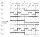
- FIG. 3 is a diagram showing output voltage polarities in each chopper phase by the switch circuit shown in FIG. Hall electromotive force V 1H , offset voltage V 1O of Hall sensor 1, offset voltage V 2O of differential amplifier 5, Hall electromotive force V 1H ′ demodulated by the third switch circuit 6, offset voltage V 1O of Hall sensor 1
- the polarity of the offset voltage V 2 O ′ of the differential amplifier 5 is as shown in FIG. While the chopper operation of 0 ° to 270 ° is repeated n times, the integrator 7 integrates and amplifies the output differential voltage V 2 of the third switch circuit 6.
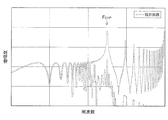
- FIG. 4 is a diagram showing an output waveform of the integrator in FIG.
- the output V 3 of the integrator 7 is represented by the formula (9), a voltage waveform as shown in FIG.
- V 1H_INT is integral amplified waveform V IH component at the output V 3 of the integrator 7
- V 1O_INT is integral amplified waveform V 1O component at the output V 3 of the integrator 7
- V 2O_INT the integrator 7 an integral amplification waveform of V. 2O component at the output V 3 of the.
- FIG. 5 is a diagram illustrating frequency characteristics of a chopper modulation transfer function with respect to noise of the Hall sensor.
- JP 2005-283503 A JP 2008-286695 A JP2011-137716A
- the amplification of the integrator 7 is set so as not to exceed the operating voltage range during chopper operation of 0 ° ⁇ 270 °.
- the amplification degree of the integrator 7 is limited by the offset voltage V 1O of the Hall sensor 1 and the Hall electromotive force V 1H Cannot be amplified sufficiently.
- the amplification factor of the integrator 7 of the offset voltage V 1O of the Hall sensor 1 per one phase of the chopper is halved, so that the operating voltage range in the integrator 7 is reduced while maintaining the amplification factor and integration time of the integrator 7. It can be greatly suppressed.
- the output of the differential amplifier 5 is used.
- the band is limited to a low band, since the chopper modulation frequency of the Hall electromotive force V 1H is doubled by setting the chopper modulation frequency to 2F CHP , a settling error due to insufficient band occurs in the differential amplifier 5.
- the signal loss of the Hall electromotive force V 1H increases during demodulation by the third switch circuit 6, and the amplification factor of the Hall electromotive force signal V 1H of the entire system decreases, leading to S / N degradation. is there.
- the output bandwidth of the differential amplifier 5 is strongly dependent on temperature, resulting in even temperature fluctuations of the output voltage V 3 of the integrator 7 is a problem that increases.
- the settling time of the differential amplifier is finite, and the settling time at the rising time of the input voltage is different from the settling time at the falling time.
- the transition order of each chopper phase is devised as 0 ° ⁇ 90 ° ⁇ 270 ° ⁇ 180 °, etc., the offset voltage of the Hall sensor and the offset voltage of the differential amplifier are removed with high accuracy.
- the phase states of 0 °, 90 °, 180 °, and 270 ° within one chopper period, and the output currents are reversed with the same bias current direction, and 0 ° ′, 90 ° ′, 180 ° ′, and 270 It is not a periodic combination of the phase states of '°, and even if the chopper modulation frequency of the offset voltage is increased, the integration unit does not cause signal loss of the Hall electromotive force.
- the definitive operating voltage range in which no effect can be obtained that considerably suppress.
- the magnetic detection device described in Patent Document 2 described above randomly changes the order of transition of two states such as the chopper phase (0 °, 270 °), and spreads the disturbance noise received by the amplifier or the like. While achieving high-speed response while effectively removing noise, the phase state of 0 °, 90 °, 180 °, 270 ° within one chopper period, as in the present invention, It is not a periodic combination of 0 ° ', 90 °', 180 ° ', 270 °' phase states in which the bias current direction is the same and the output terminal is inverted, and even if the chopper modulation frequency of the offset voltage is increased. The effect of significantly suppressing the operating voltage range in the integration section without incurring signal loss of Hall electromotive force cannot be obtained.
- the magnetic detection device described in Patent Document 3 described above adds or subtracts the reference voltage Vref in synchronization with the Hall sensor output that is changed in the order of 0 ° ⁇ 90 ° ⁇ 270 ° ⁇ 180 ° and is chopper modulated.
- the offset voltage of the Hall sensor and the analog element can be removed with high accuracy and the Hall electromotive force can be detected with high accuracy.
- phase states of 0 °, 90 °, 180 °, and 270 ° within one cycle of the chopper and 0 ° ′, 90 ° ′, 180 ° ′, and 270 ° in which the output terminal is inverted with the same bias current direction. It is not a periodic combination of phase states, and even if the chopper modulation frequency of the offset voltage is increased, the operating voltage in the integration section does not cause signal loss of Hall electromotive force. It is those which do not effect was obtained that significantly inhibit the circumference.
- the present invention has been made in view of such a problem, and an object of the present invention is to increase the chopper modulation frequency of the offset voltage of the Hall sensor so that the integration part of the offset voltage of the Hall sensor in the integration part.
- An object of the present invention is to provide a magnetic detection device and a magnetic detection method capable of suppressing an amplification degree and greatly suppressing an operating voltage range in an integration unit.
- a magnetic detection device is connected to a Hall sensor that detects magnetism, a bias generation unit that drives the Hall sensor, and the Hall sensor.
- the polarity of the Hall electromotive force of the Hall sensor is the first polarity
- the polarity of the Hall offset voltage of the Hall sensor alternates four times.
- the Hall electromotive force of the Hall sensor is Of the four terminals of the Hall sensor so that the polarity of the Hall sensor is a second polarity opposite to the first polarity and the polarity of the Hall offset voltage of the Hall sensor alternates four times.
- the switch unit includes the bias generation unit and the first unit so that a current flows from the first terminal of the Hall sensor toward the second terminal opposite to the first terminal in the first period.
- the first terminal and the second terminal are connected, and the third terminal of the Hall sensor and the fourth terminal facing the third terminal are connected to the positive input terminal and the negative input terminal of the amplifying unit, respectively.
- a second switching unit that connects the first terminal to the positive input terminal and the negative input terminal of the amplification unit, respectively, and the bias generation unit so that a current flows from the second terminal toward the first terminal.
- the bias generator and the fourth and third terminals are connected so as to flow, and the first and second terminals are connected to the positive input terminal and the negative input terminal of the amplifier, respectively. And switching the bias generator and the first and second terminals so that a current flows from the first terminal toward the second terminal in the second period, and , A fifth switching for connecting the fourth and third terminals to the positive input terminal and the negative input terminal of the amplifying unit, respectively, and a current flows from the third terminal toward the fourth terminal.
- the bias generator and the third and fourth And a sixth switch for connecting the first and second terminals to the positive input terminal and the negative input terminal of the amplifier, respectively, and from the second terminal to the first terminal.
- the bias generator and the second and first terminals are connected so that current flows in the direction, and the third and fourth terminals are connected to the positive input terminal and the negative input terminal of the amplifier, respectively.
- the switch unit repeatedly performs switching in the first period n times (n is an integer of 2 or more), repeatedly switches in the second period n times, and the inversion unit includes the amplification unit Is inverted in synchronization with the switching between the first period and the second period.
- the direction of the current from the bias generation unit is switched with respect to two opposing terminals among the four terminals of the Hall sensor, a Hall generation unit that drives the Hall sensor, and a Hall generation unit that drives the Hall sensor.
- a switch unit that switches a direction of a voltage to be extracted with respect to two opposing terminals in a direction orthogonal to the direction of the current, an amplification unit that amplifies the voltage extracted by switching by the switch unit, An inversion unit for inverting the polarity of the voltage from the amplification unit, and the operating frequency when the polarity of the Hall offset voltage of the Hall sensor is alternated, the operating frequency when the polarity of the Hall electromotive force of the Hall sensor is alternated 2n times (n is an integer of 1 or more).
- the Hall sensor is connected in the first period by a switch unit connected to the Hall sensor.
- the polarity of the Hall electromotive force of the Hall sensor is the first polarity, so that the polarity of the Hall offset voltage of the Hall sensor alternates four times, the current of the two terminals facing each other among the four terminals of the Hall sensor.
- the polarity of the Hall electromotive force of the Hall sensor is a second polarity opposite to the first polarity, and the Hall sensor Hall
- the direction of the current is switched with respect to two opposing terminals of the four terminals of the Hall sensor so that the polarity of the offset voltage alternates four times, and is opposed in a direction orthogonal to the direction of the current.
- the step of switching the direction of the voltage to be extracted with respect to the two terminals the step of amplifying the voltage extracted by the switching by the switch unit by the amplification unit, and the switching of the current and voltage by the switch unit.
- the present invention by increasing the chopper modulation frequency of the offset voltage of the Hall sensor, the amplification degree of the integration part of the Hall sensor offset voltage in the integration part is suppressed, and the operating voltage range in the integration part is greatly suppressed.
- the magnetic detection device and the magnetic detection method can be realized.
- FIG. 1 is a circuit configuration diagram for explaining a conventional magnetic detection device.
- FIGS. 2A to 2D are diagrams showing the connection state of the Hall sensor in each chopper phase by the switch circuit shown in FIG.
- FIG. 3 is a diagram showing output voltage polarities in each chopper phase by the switch circuit shown in FIG.
- FIG. 4 is a diagram showing an output waveform of the integrator in FIG.
- FIG. 5 is a diagram illustrating frequency characteristics of a chopper modulation transfer function with respect to noise of the Hall sensor.
- FIG. 6 is a circuit configuration diagram for explaining an embodiment of the magnetic detection device according to the present invention.
- 7A to 7H are diagrams showing the connection state of the Hall sensor in each chopper phase by the switch unit of the magnetic detection device according to the present invention shown in FIG.
- FIG. 8 is a diagram showing input / output voltage polarities of each block by the switch unit of the magnetic detection device according to the present invention shown in FIG.
- FIG. 9 is a diagram showing an output waveform of the integrator in the magnetic detection apparatus according to the present invention shown in FIG.
- FIG. 10 is a diagram showing frequency characteristics of a chopper modulation transfer function with respect to noise of the Hall sensor in the present invention.
- FIG. 11 is a flowchart for explaining the magnetic detection method according to the present invention.
- FIG. 6 is a circuit configuration diagram for explaining the magnetic detection device according to the present embodiment, in which reference numeral 11 denotes a hall sensor, 12 denotes a bias generation unit, 13 denotes a first switch unit, and 14 denotes a second switch. , 15 is a differential amplifying unit, 16 is an inverting unit (third switch unit), 17 is an integrating unit, and 18 is a switch control unit.
- the magnetic sensor includes a Hall sensor 11 that detects magnetism and a bias generation unit 12 that drives the Hall sensor 11.
- the magnetic sensor according to this embodiment shown in FIG. the polarity of the Hall electromotive force of the Hall sensor 11 is the first polarity and the polarity of the Hall offset voltage of the Hall sensor 11 is changed four times during the first period.
- the Hall sensor 11 has a second polarity opposite to the first polarity of the Hall electromotive force, and the Hall sensor 11 has a polarity of the Hall offset voltage that alternates four times.
- the direction of the current from the bias generation unit 12 is switched with respect to two opposing terminals of the four terminals of the sensor 11, and the two terminals facing each other in the direction orthogonal to the current direction are switched.
- the direction of the voltage to be extracted is switched.
- the differential amplifying unit 15 amplifies the voltage extracted by switching by the switch units 13 and 14.
- the inversion unit 16 inverts the polarity of the voltage from the amplification unit 15 in synchronization with the switching between the first period and the second period among the switching of the current and voltage by the switch units 13 and 14.
- the integrating unit 17 integrates the voltage extracted by the polarity inversion by the inverting unit 16.
- FIGS. 7A to 7H are diagrams showing the connection state of the Hall sensor in each chopper phase by the switch unit of the magnetic detection device according to the present embodiment shown in FIG.
- the first and second switch sections 13 and 14 generate a bias so that a current flows from the first terminal of the Hall sensor 11 toward the second terminal opposite to the first terminal in the first period.
- the fourth terminal opposite to the third terminal of the Hall sensor 11 is connected to the positive input terminal and the negative terminal of the differential amplifier 15.
- the first switching (FIG. 7A) connected to each of the input terminals, and the bias generator 12 and the third and fourth terminals so that a current flows from the third terminal toward the fourth terminal.
- switching the second and first terminals to the positive input terminal and the negative input terminal of the differential amplifying unit 15 respectively (FIG.
- a third switch for connecting the first terminal and connecting the fourth and third terminals to the positive input terminal and the negative input terminal of the differential amplifier unit 15, respectively;
- the bias generator 12 and the fourth and third terminals are connected so that a current flows from the terminal 4 to the third terminal, and the first and second terminals are connected to the differential amplifier 15.
- the fourth switching (FIG. 7 (d)) connected to the positive input terminal and the negative input terminal is performed.
- first and second switch units 13 and 14 have the bias generation unit 12 and the first and second terminals so that current flows from the first terminal toward the second terminal in the second period.
- the fifth switching (FIG. 7 (e)) for connecting the fourth and third terminals to the positive input terminal and the negative input terminal of the differential amplifying unit 15, respectively, and from the third terminal
- the bias generator 12 is connected to the third and fourth terminals so that current flows toward the fourth terminal, and the first and second terminals are connected to the positive input terminal of the differential amplifier 15 and
- a sixth switch (FIG. 7 (f)) connected to each negative input terminal, and the bias generator 12 and the second and first terminals so that a current flows from the second terminal toward the first terminal.
- the third and fourth terminals are connected to the positive input terminal and the negative terminal of the differential amplifying unit 15, respectively.
- the seventh switch (FIG. 7 (g)) connected to each of the power terminals, and the bias generator 12 and the fourth and third terminals so that current flows from the fourth terminal to the third terminal.
- the eighth switching (FIG. 7 (h)) for connecting the second and first terminals to the positive input terminal and the negative input terminal of the differential amplifying unit 15, respectively. Yes.
- 0 ° ′, 90 ° ′, 180 ° ′, and 270 ° ′ have the same bias current direction as 0 °, 90 °, 180 °, and 270 °, respectively, and are equal to a connection state in which the output terminal is inverted.
- the differential amplifying unit 15 amplifies the output differential voltage V 1 of the second switch unit 14 and the inherent offset voltage V 2 O of the differential amplifying unit 15 with a constant magnification A.
- the output differential voltage of the differential amplification unit 15 is demodulated and supplied to the integration unit 17.
- Inverting unit output differential voltage V 2 of the (third switching section) 16 is expressed by Equation (18) to (25).
- FIG. 8 is a diagram illustrating input / output voltage polarities of each block by the switch unit of the magnetic detection device according to the present embodiment illustrated in FIG. 6. Hall electromotive force V 1H , Hall offset V 1O , offset V 2O of differential amplifier 15 and Hall electromotive force V 1H ′ demodulated by third switch unit 16, Hall offset V 1O ′, differential amplifier 15 The polarity of the offset V 2 O ′ is as shown in FIG.
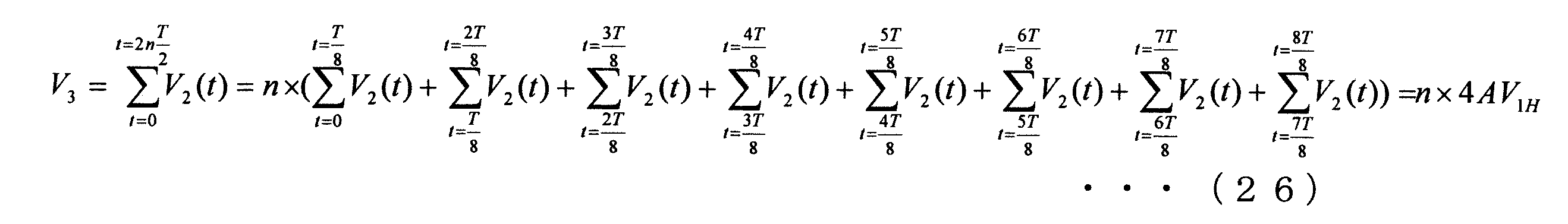
- FIG. 9 is a diagram illustrating an output waveform of the integrator in the magnetic detection device according to the present embodiment illustrated in FIG. 6. While the integration unit 17 repeats the chopper operation n times, the output differential voltage of the third switch unit 16 is integrated and amplified. Output voltage V 3 of the integrator 17 is represented by the formula (26), a voltage waveform as shown in FIG.
- the first and second switch units 13 and 14 repeat switching in the first period n times (n is an integer of 2 or more), repeatedly switching in the second period n times, and the inversion unit. 16 inverts the polarity of the voltage from the differential amplifier 15 in synchronization with the switching between the first period and the second period.
- a magnetic detection device includes a Hall sensor 11 that detects magnetism, a bias generation unit 12 that drives the Hall sensor 11, and two opposing terminals of the four terminals of the Hall sensor 11.
- First and second switches for switching the direction of the current from the bias generator 12 with respect to the terminal and for switching the direction of the voltage to be extracted with respect to two opposing terminals in a direction orthogonal to the direction of the current Units 13 and 14, a differential amplifier 15 for amplifying the voltage extracted by switching by the first and second switch units 13 and 14, and an inversion for inverting the polarity of the voltage from the differential amplifier 15 Unit 16 and an integration unit 17 that integrates the voltage extracted by the inversion of polarity by the inversion unit 16 and exchanges the polarity of the Hall offset voltage of the Hall sensor 11.
- Operating frequency at which the, 2n times than the operating frequency at which the alternating polarity of the Hall electromotive force of the Hall sensor 11 are configured such that.
- FIG. 10 is a diagram showing frequency characteristics of a chopper modulation transfer function with respect to noise of the Hall sensor in the present invention.
- phase states of 0 °, 90 °, 180 °, and 270 ° are the same as those of 0 ° ′, 90 ° ′, 180 ° ′, and 270 ° in which the output terminal is inverted with the same bias current direction.
- a similar effect can be obtained by combining the phase states during one demodulation period in the third switch circuit 16. For example, a combination of 0 ° ⁇ 270 ° ′ ⁇ 90 ° ⁇ 180 ° ′ ⁇ 0 ° ′ ⁇ 270 ° ⁇ 180 ° ⁇ 90 ° ′ can be considered.
- the Hall electromotive force V 1H is increased.
- the chopper modulation frequency of the offset voltage V 1O unique to the hall sensor can be increased up to 2a times with respect to the chopper modulation frequency F CHP , and the above-described effects can be further enhanced.
- the integrating unit 17 integrates the voltage extracted by polarity inversion by the inverting unit 16, but is not limited to this, and from the amplifying unit 15 by the integrating unit 17. After the voltage integration, the polarity of the voltage may be reversed by the inverting unit 16. Further, in the above-described embodiment of the present invention, the Hall sensor 11 is current-driven by the bias generation unit 12. However, the present invention is not limited to this, and the Hall sensor 11 may be voltage-driven by the bias voltage generation unit. .
- FIG. 11 is a diagram illustrating a flowchart for explaining the magnetic detection method according to the present embodiment.
- the Hall electromotive force of the Hall sensor 11 has a first polarity
- the Hall sensor 11 has a Hall offset voltage of 4 times alternating polarity.
- the direction of the current is switched with respect to two opposing terminals among the four terminals of 11, and the direction of the voltage to be taken out with respect to the two opposing terminals in a direction orthogonal to the direction of the current is switched ( Step S1).
- the polarity of the Hall electromotive force of the Hall sensor 11 is the second polarity opposite to the first polarity, and the polarity of the Hall offset voltage of the Hall sensor 11 alternates four times.
- the direction of the current to be switched with respect to two opposing terminals of the four terminals of the Hall sensor 11 and to be taken out with respect to the two opposing terminals in a direction orthogonal to the direction of the current Are switched (step S2).
- step S3 the voltage extracted by switching is amplified (step S3).
- step S4 the polarity of the amplified voltage is inverted in synchronization with the switching between the first period and the second period among the switching between the current and the voltage (step S4).
- step S5 the voltage extracted by inversion is integrated (step S5).
Abstract
Description
また、ホール素子は、入力された磁界の強度に応じたホール起電力信号を発生する磁電変換機能を有するため、磁気センサとして広く用いられている。しかしながら、ホール素子には、磁場が零である状態、すなわち、無磁場の状態でも、零でない有限の電圧が出力されてしまうというオフセット電圧(不平衡電圧)が存在する。
ホールセンサを採用した磁気検出装置においては、ホール素子がオフセット電圧を有することから、このオフセット電圧を除去することが行われており、その一例としては、非特許文献1に記載のspinning current principleが知られている。
さらに、例えば、特許文献3に記載のものは、磁気検出センサのオフセット電圧とアナログ回路のアナログ素子のオフセット電圧とを高精度に除去し、磁気検出センサの磁気を高精度に検出することのできる磁気検出装置に関するものである。
第1のスイッチ回路3と第2のスイッチ回路4とを制御することで、ホールセンサ1の4端子のうち対向する2端子の間にバイアス電流を供給し、4端子のうち残りの対向する2端子を差動増幅器5に接続する。
ここで、ホールセンサ1の出力差動電圧V1は、Vhp-Vhnで定義されるものとする。


図4は、図1における積分器の出力波形を示す図である。積分器7の出力V3は、式(9)で表され、図4に示すような電圧波形となる。

第1のスイッチ回路3乃至第3のスイッチ回路6によりチョッパー変調することで、0°~270°のチョッパー動作1回ごとにホールセンサ1のオフセット電圧V1O及び差動増幅器5のオフセット電圧V2Oをキャンセルアウトし、ホール起電力V1Hのみを積分増幅することが可能となる。
図6は、本実施形態に係る磁気検出装置を説明するための回路構成図で、図中符号11はホールセンサ、12はバイアス生成部、13は第1のスイッチ部、14は第2のスイッチ部、15は差動増幅部、16は反転部(第3のスイッチ部)、17は積分部、18はスイッチ制御部を示している。
第1及び第2のスイッチ部13,14は、第1期間において、ホールセンサ11の第1の端子からこの第1の端子に対向する第2の端子に向かって電流が流れるように、バイアス生成部12と第1及び第2の端子とを接続し、かつ、ホールセンサ11の第3の端子及びこの第3の端子に対向する第4の端子を差動増幅部15の正入力端子及び負入力端子にそれぞれ接続する第1の切り換え(図7(a))と、第3の端子から第4の端子に向かって電流が流れるように、バイアス生成部12と第3及び第4の端子とを接続し、かつ、第2及び第1の端子を差動増幅部15の正入力端子及び負入力端子にそれぞれ接続する第2の切り換え(図7(b))と、第2の端子から第1の端子に向かって電流が流れるように、バイアス生成部12と第2及び第1の端子とを接続し、かつ、第4及び第3の端子を差動増幅部15の正入力端子及び負入力端子にそれぞれ接続する第3の切り換え(図7(c))と、第4の端子から第3の端子に向かって電流が流れるように、バイアス生成部12と第4及び第3の端子とを接続し、かつ、第1及び第2の端子を差動増幅部15の正入力端子及び負入力端子にそれぞれ接続する第4の切り換え(図7(d))とを行うように構成されている。
これにより、ホール起電力V1H及びホールセンサ11のオフセット電圧V1Oの加算である第2のスイッチ部14の出力差動電圧V1は、式(10)乃至(17)で表される。0°’、90°’、180°’、270°’は、それぞれ0°、90°、180°、270°とバイアス電流方向が同じで、出力端子を反転させた接続状態に等しい。


図9は、図6に示した本実施形態に係る磁気検出装置における積分器の出力波形を示す図である。積分部17にてチョッパー動作をn回繰り返す間、第3のスイッチ部16の出力差動電圧を積分増幅する。積分部17の出力電圧V3は、式(26)で表され、図9のような電圧波形となる。
このように、ホールセンサのオフセット電圧のチョッパー変調周波数を速くすることで、積分部におけるホールセンサのオフセット電圧の積分部の増幅度を抑制し、積分部における動作電圧範囲を大幅に抑制することができるような磁気検出装置を実現することができる。
また、上述した本発明の実施形態では、バイアス生成部12によりホールセンサ11を電流駆動するものであるが、これに限るものではなく、バイアス電圧生成部によりホールセンサ11を電圧駆動するものでもよい。
このように、ホールセンサのオフセット電圧のチョッパー変調周波数を速くすることで、積分部におけるホールセンサのオフセット電圧の積分部の増幅度を抑制し、積分部における動作電圧範囲を大幅に抑制することができるような磁気検出方法を実現することができる。
2 バイアス電流生成回路
3 第1のスイッチ回路
4 第2のスイッチ回路
5 差動増幅器
6 第3のスイッチ回路
7 積分器
8 スイッチ制御回路
12 バイアス生成部
13 第1のスイッチ部
14 第2のスイッチ部
15 差動増幅部
16 反転部(第3のスイッチ部)
17 積分部
18 スイッチ制御部
Claims (5)
- 磁気を検出するホールセンサと、
該ホールセンサを駆動するバイアス生成部と、
前記ホールセンサに接続され、第1期間において、前記ホールセンサのホール起電力の極性は第1の極性で、前記ホールセンサのホールオフセット電圧の極性が4回交番し、第2期間において、前記ホールセンサのホール起電力の極性が前記第1の極性とは逆の極性の第2の極性で、前記ホールセンサのホールオフセット電圧の極性が4回交番するように、前記ホールセンサの4つの端子のうちの対向する2つの端子に対して前記バイアス生成部からの電流の向きを切り換え、かつ、該電流の向きに直交する方向にあって対向する2つの端子に対して取り出す電圧の向きを切り換えるスイッチ部と、
該スイッチ部による切り換えにより取り出された電圧を増幅する増幅部と、
前記スイッチ部による電流及び電圧の切り換えのうち、前記第1期間と前記第2期間の切り換えに同期して、前記増幅部からの電圧の極性を反転させる反転部と、
を備えていることを特徴とする磁気検出装置。 - 前記スイッチ部は、
前記第1期間において、
前記ホールセンサの第1の端子から該第1の端子に対向する第2の端子に向かって電流が流れるように、前記バイアス生成部と前記第1及び第2の端子とを接続し、かつ、前記ホールセンサの第3の端子及び該第3の端子に対向する第4の端子を前記増幅部の正入力端子及び負入力端子にそれぞれ接続する第1の切り換えと、
前記第3の端子から前記第4の端子に向かって電流が流れるように、前記バイアス生成部と前記第3及び第4の端子とを接続し、かつ、前記第2及び第1の端子を前記増幅部の正入力端子及び負入力端子にそれぞれ接続する第2の切り換えと、
前記第2の端子から前記第1の端子に向かって電流が流れるように、前記バイアス生成部と前記第2及び第1の端子とを接続し、かつ、前記第4及び第3の端子を前記増幅部の正入力端子及び負入力端子にそれぞれ接続する第3の切り換えと、
前記第4の端子から前記第3の端子に向かって電流が流れるように、前記バイアス生成部と前記第4及び第3の端子とを接続し、かつ、前記第1及び第2の端子を前記増幅部の正入力端子及び負入力端子にそれぞれ接続する第4の切り換えと、
前記第2期間において、
前記第1の端子から前記第2の端子に向かって電流が流れるように、前記バイアス生成部と前記第1及び第2の端子とを接続し、かつ、前記第4及び第3の端子を前記増幅部の正入力端子及び負入力端子にそれぞれ接続する第5の切り換えと、
前記第3の端子から前記第4の端子に向かって電流が流れるように、前記バイアス生成部と前記第3及び第4の端子とを接続し、かつ、前記第1及び第2の端子を前記増幅部の正入力端子及び負入力端子にそれぞれ接続する第6の切り換えと、
前記第2の端子から前記第1の端子に向かって電流が流れるように、前記バイアス生成部と前記第2及び第1の端子とを接続し、かつ、前記第3及び第4の端子を前記増幅部の正入力端子及び負入力端子にそれぞれ接続する第7の切り換えと、
前記第4の端子から前記第3の端子に向かって電流が流れるように、前記バイアス生成部と前記第4及び第3の端子とを接続し、かつ、前記第2及び第1の端子を前記増幅部の正入力端子及び負入力端子にそれぞれ接続する第8の切り換えと
を行うことを特徴とする請求項1に記載の磁気検出装置。 - 前記スイッチ部は、前記第1の期間のおける切り換えをn回(nは2以上の整数)繰り返し行い、前記第2の期間における切り換えをn回繰り返し行い、
前記反転部は、前記増幅部からの電圧の極性を、前記第1期間と前記第2期間の切り換えに同期して反転させることを特徴とする請求項1又は2に記載の磁気検出装置。 - 磁気を検出するホールセンサと、
該ホールセンサを駆動するバイアス生成部と、
前記ホールセンサの4つの端子のうちの対向する2つの端子に対して前記バイアス生成部からの電流の向きを切り換え、かつ、該電流の向きに直交する方向にあって対向する2つの端子に対して取り出す電圧の向きを切り換えるスイッチ部と、
該スイッチ部による切り換えにより取り出された電圧を増幅する増幅部と、
該増幅部からの電圧の極性を反転させる反転部とを備え、
前記ホールセンサのホールオフセット電圧の極性を交番するときの動作周波数が、前記ホールセンサのホール起電力の極性を交番するときの動作周波数よりも2n倍(nは1以上の整数)であることを特徴とする磁気検出装置。 - 磁気を検出するホールセンサと、該ホールセンサを駆動するバイアス生成部とを備えた磁気検出装置における磁気検出方法において、
前記ホールセンサに接続されたスイッチ部により、第1期間において、ホールセンサのホール起電力の極性は第1の極性で、前記ホールセンサのホールオフセット電圧の極性が4回交番するように、前記ホールセンサの4つの端子のうちの対向する2つの端子に対して電流の向きを切り換え、かつ、該電流の向きに直交する方向にあって対向する2つの端子に対して取り出す電圧の向きを切り換えるステップと、
前記ホールセンサに接続されたスイッチ部により、第2期間において、前記ホールセンサのホール起電力の極性が前記第1の極性とは逆の極性の第2の極性で、前記ホールセンサのホールオフセット電圧の極性が4回交番するように、前記ホールセンサの4つの端子のうちの対向する2つの端子に対して電流の向きを切り換え、かつ、該電流の向きに直交する方向にあって対向する2つの端子に対して取り出す電圧の向きを切り換えるステップと、
前記スイッチ部による切り換えにより取り出された電圧を増幅部により増幅するステップと、
前記スイッチ部による前記電流及び電圧の切り換えのうち、前記第1期間と前記第2期間の切り換えに同期して、前記増幅された電圧の極性を反転部により反転させるステップと
を有することを特徴とする磁気検出方法。
Priority Applications (5)
| Application Number | Priority Date | Filing Date | Title |
|---|---|---|---|
| EP13787904.5A EP2848957B1 (en) | 2012-05-11 | 2013-04-08 | Magnetism detection device and magnetism detection method |
| CN201380002444.2A CN103733082B (zh) | 2012-05-11 | 2013-04-08 | 磁检测装置以及磁检测方法 |
| US14/235,488 US9395422B2 (en) | 2012-05-11 | 2013-04-08 | Magnetism detection device and magnetism detection method |
| JP2013548693A JP5695764B2 (ja) | 2012-05-11 | 2013-04-08 | 磁気検出装置及び磁気検出方法 |
| KR1020137033556A KR101542679B1 (ko) | 2012-05-11 | 2013-04-08 | 자기 검출 장치 및 자기 검출 방법 |
Applications Claiming Priority (2)
| Application Number | Priority Date | Filing Date | Title |
|---|---|---|---|
| JP2012-109728 | 2012-05-11 | ||
| JP2012109728 | 2012-05-11 |
Publications (1)
| Publication Number | Publication Date |
|---|---|
| WO2013168353A1 true WO2013168353A1 (ja) | 2013-11-14 |
Family
ID=49550423
Family Applications (1)
| Application Number | Title | Priority Date | Filing Date |
|---|---|---|---|
| PCT/JP2013/002404 WO2013168353A1 (ja) | 2012-05-11 | 2013-04-08 | 磁気検出装置及び磁気検出方法 |
Country Status (6)
| Country | Link |
|---|---|
| US (1) | US9395422B2 (ja) |
| EP (1) | EP2848957B1 (ja) |
| JP (1) | JP5695764B2 (ja) |
| KR (1) | KR101542679B1 (ja) |
| CN (1) | CN103733082B (ja) |
| WO (1) | WO2013168353A1 (ja) |
Cited By (2)
| Publication number | Priority date | Publication date | Assignee | Title |
|---|---|---|---|---|
| JP2017142068A (ja) * | 2016-02-08 | 2017-08-17 | 株式会社ユー・アール・ディー | 電流センサ及びそのフィルタリング方法 |
| JP2018151257A (ja) * | 2017-03-13 | 2018-09-27 | エイブリック株式会社 | 磁気センサ回路 |
Families Citing this family (10)
| Publication number | Priority date | Publication date | Assignee | Title |
|---|---|---|---|---|
| US10191505B2 (en) * | 2014-11-07 | 2019-01-29 | Diodes Incorporated | Hall sensor chip with timing control |
| US10386392B2 (en) * | 2015-01-28 | 2019-08-20 | Hioki Denki Kabushiki Kaisha | Hall element driving circuit, sensor circuit, and current measuring apparatus |
| EP3396397B1 (en) * | 2017-04-28 | 2019-11-20 | Melexis Technologies SA | Bridge sensor biasing and readout |
| EP3401646B1 (en) * | 2017-05-09 | 2020-04-15 | Melexis Technologies SA | Bridge sensor error check |
| CN109387795B (zh) * | 2017-08-09 | 2021-01-01 | 苏州市灵矽微系统有限公司 | 一种cmos磁传感器模拟前端电路 |
| EP3591417B1 (en) * | 2018-07-05 | 2020-06-10 | Melexis Technologies SA | Randomized spinning of hall plates |
| IT201800007246A1 (it) * | 2018-07-17 | 2020-01-17 | Sensore di hall, dispositivi e procedimento corrispondenti | |
| JP2021113538A (ja) * | 2020-01-20 | 2021-08-05 | 日立Astemo株式会社 | 電磁弁駆動装置 |
| US11333718B2 (en) * | 2020-04-15 | 2022-05-17 | Allegro Microsystems, Llc | Sensors having dynamic phase compensation |
| US11333719B2 (en) * | 2020-09-09 | 2022-05-17 | Texas Instruments Incorporated | Hall-effect sensor with reduced offset voltage |
Citations (5)
| Publication number | Priority date | Publication date | Assignee | Title |
|---|---|---|---|---|
| JP2005283503A (ja) | 2004-03-30 | 2005-10-13 | Asahi Kasei Electronics Co Ltd | 磁気検出装置 |
| WO2007116823A1 (ja) * | 2006-04-03 | 2007-10-18 | Asahi Kasei Emd Corporation | ホール素子及び磁気センサ |
| JP2008286695A (ja) | 2007-05-18 | 2008-11-27 | Asahi Kasei Electronics Co Ltd | 磁気検出装置 |
| JP2009544004A (ja) * | 2006-07-14 | 2009-12-10 | フラウンホッファー−ゲゼルシャフト ツァ フェルダールング デァ アンゲヴァンテン フォアシュンク エー.ファオ | オフセットを受けるセンサ信号を処理するための方法及びその方法を実行するために設計されるセンサ装置 |
| JP2011137716A (ja) | 2009-12-28 | 2011-07-14 | Asahi Kasei Electronics Co Ltd | 磁気検出装置 |
Family Cites Families (11)
| Publication number | Priority date | Publication date | Assignee | Title |
|---|---|---|---|---|
| JP3492009B2 (ja) * | 1995-03-16 | 2004-02-03 | ジーイー横河メディカルシステム株式会社 | Mri用コイル装置 |
| US6046944A (en) * | 1998-01-28 | 2000-04-04 | Sun Microsystems, Inc. | Bias generator circuit for low voltage applications |
| DE19931292C2 (de) * | 1999-07-07 | 2001-05-17 | Siemens Ag | Pulssequenz für ein MR-Tomographiegerät und MR-Tomographiegerät zur Durchführung der Pulssequenz |
| DE10032530C2 (de) * | 2000-07-05 | 2002-10-24 | Infineon Technologies Ag | Verstärkerschaltung mit Offsetkompensation |
| US6794863B2 (en) * | 2002-11-13 | 2004-09-21 | Matsushta Electric Industrial Co., Ltd. | Magnetic field sensor, method for detecting magnetic field and device for detecting magnetic field |
| KR101109712B1 (ko) | 2006-09-07 | 2012-01-31 | 알프스 덴키 가부시키가이샤 | 자기검출장치 |
| US7425821B2 (en) * | 2006-10-19 | 2008-09-16 | Allegro Microsystems, Inc. | Chopped Hall effect sensor |
| JP5052982B2 (ja) | 2007-07-25 | 2012-10-17 | セイコーインスツル株式会社 | 磁気センサ回路 |
| US20110187359A1 (en) * | 2008-05-30 | 2011-08-04 | Tobias Werth | Bias field generation for a magneto sensor |
| JP4675994B2 (ja) * | 2008-08-27 | 2011-04-27 | 株式会社東芝 | 磁気センサ及び磁気測定方法 |
| JP2011163928A (ja) * | 2010-02-09 | 2011-08-25 | Asahi Kasei Electronics Co Ltd | ホール起電力信号検出装置 |
-
2013
- 2013-04-08 KR KR1020137033556A patent/KR101542679B1/ko active IP Right Grant
- 2013-04-08 WO PCT/JP2013/002404 patent/WO2013168353A1/ja active Application Filing
- 2013-04-08 JP JP2013548693A patent/JP5695764B2/ja not_active Expired - Fee Related
- 2013-04-08 US US14/235,488 patent/US9395422B2/en not_active Expired - Fee Related
- 2013-04-08 EP EP13787904.5A patent/EP2848957B1/en not_active Not-in-force
- 2013-04-08 CN CN201380002444.2A patent/CN103733082B/zh not_active Expired - Fee Related
Patent Citations (5)
| Publication number | Priority date | Publication date | Assignee | Title |
|---|---|---|---|---|
| JP2005283503A (ja) | 2004-03-30 | 2005-10-13 | Asahi Kasei Electronics Co Ltd | 磁気検出装置 |
| WO2007116823A1 (ja) * | 2006-04-03 | 2007-10-18 | Asahi Kasei Emd Corporation | ホール素子及び磁気センサ |
| JP2009544004A (ja) * | 2006-07-14 | 2009-12-10 | フラウンホッファー−ゲゼルシャフト ツァ フェルダールング デァ アンゲヴァンテン フォアシュンク エー.ファオ | オフセットを受けるセンサ信号を処理するための方法及びその方法を実行するために設計されるセンサ装置 |
| JP2008286695A (ja) | 2007-05-18 | 2008-11-27 | Asahi Kasei Electronics Co Ltd | 磁気検出装置 |
| JP2011137716A (ja) | 2009-12-28 | 2011-07-14 | Asahi Kasei Electronics Co Ltd | 磁気検出装置 |
Non-Patent Citations (2)
| Title |
|---|
| A.BAKKER; A.A.BELLEKOM; S.MIDDELHOEKAND; J.H. HUIJSING: "Low - Offset Low - Noise 3.5mW CMOS Spinning - Current Hall Effect Sensor With Integrated Chopper Amplifier", THE 13TH EUROPEAN CONFERENCE ON SOLID - STATE TRANSDUCERS, 12 September 1999 (1999-09-12), pages 1045 - 1048 |
| See also references of EP2848957A4 * |
Cited By (2)
| Publication number | Priority date | Publication date | Assignee | Title |
|---|---|---|---|---|
| JP2017142068A (ja) * | 2016-02-08 | 2017-08-17 | 株式会社ユー・アール・ディー | 電流センサ及びそのフィルタリング方法 |
| JP2018151257A (ja) * | 2017-03-13 | 2018-09-27 | エイブリック株式会社 | 磁気センサ回路 |
Also Published As
| Publication number | Publication date |
|---|---|
| EP2848957B1 (en) | 2017-03-29 |
| EP2848957A4 (en) | 2016-01-20 |
| CN103733082A (zh) | 2014-04-16 |
| JPWO2013168353A1 (ja) | 2015-12-24 |
| US9395422B2 (en) | 2016-07-19 |
| CN103733082B (zh) | 2016-06-22 |
| KR20140013083A (ko) | 2014-02-04 |
| US20140210462A1 (en) | 2014-07-31 |
| JP5695764B2 (ja) | 2015-04-08 |
| KR101542679B1 (ko) | 2015-08-06 |
| EP2848957A1 (en) | 2015-03-18 |
Similar Documents
| Publication | Publication Date | Title |
|---|---|---|
| JP5695764B2 (ja) | 磁気検出装置及び磁気検出方法 | |
| JP5385490B1 (ja) | ホール起電力信号検出回路及びその電流センサ | |
| US6674322B2 (en) | Amplifier circuit with offset compensation | |
| JP5802187B2 (ja) | ホール起電力信号検出回路及びその電流センサ | |
| JP2017227626A (ja) | 磁気センサ集積回路、モータ組立体及び応用装置 | |
| US9354279B2 (en) | Magnetic sensor device for generating an output in accordance with a magnetic field intensity applied to a magnetoelectric conversion hall effect element | |
| JP2017527807A (ja) | オフセット補償を用いるホール効果センサー回路 | |
| JP6297782B2 (ja) | ホール起電力信号検出回路及びその電流センサ | |
| CN106931995B (zh) | 一种基于电流输出模式的四相旋转电流电路和方法 | |
| JP4514104B2 (ja) | 磁気検出装置 | |
| WO2014155908A1 (ja) | ホール起電力信号検出回路及びその電流センサ並びにホール素子の駆動方法 | |
| JP2004309386A (ja) | 電流検出装置 | |
| JP6445360B2 (ja) | 電流測定装置 | |
| KR101197947B1 (ko) | 상호 연결된 이중 홀 소자들을 구비한 홀 소자 모듈 | |
| JP2017090439A (ja) | 磁気センサ及び集積回路 | |
| JP2016125969A (ja) | ホール素子センサおよびその動作方法 | |
| JP2014150477A (ja) | 半導体装置 | |
| Jiang et al. | A current-mode CMOS Hall sensor microsystem based on four-phase current spinning technique | |
| JP4590395B2 (ja) | 電流センサおよび電流センサのオフセット除去方法 | |
| JP2021152513A (ja) | ホール素子センサおよびその動作方法 | |
| JP2021152512A (ja) | ホール素子センサおよびその動作方法 | |
| JP2008164299A (ja) | 電流センサおよび電流センサのオフセット除去方法 | |
| JP6400533B2 (ja) | 検出装置および電流センサ | |
| JP2017125783A (ja) | 信号処理回路および信号処理方法 | |
| JPH112548A (ja) | 変位量検出装置 |
Legal Events
| Date | Code | Title | Description |
|---|---|---|---|
| ENP | Entry into the national phase |
Ref document number: 2013548693 Country of ref document: JP Kind code of ref document: A |
|
| ENP | Entry into the national phase |
Ref document number: 20137033556 Country of ref document: KR Kind code of ref document: A |
|
| 121 | Ep: the epo has been informed by wipo that ep was designated in this application |
Ref document number: 13787904 Country of ref document: EP Kind code of ref document: A1 |
|
| REEP | Request for entry into the european phase |
Ref document number: 2013787904 Country of ref document: EP |
|
| WWE | Wipo information: entry into national phase |
Ref document number: 2013787904 Country of ref document: EP |
|
| WWE | Wipo information: entry into national phase |
Ref document number: 14235488 Country of ref document: US |
|
| NENP | Non-entry into the national phase |
Ref country code: DE |