WO2013164904A1 - 光学デバイス及び検出装置 - Google Patents
光学デバイス及び検出装置 Download PDFInfo
- Publication number
- WO2013164904A1 WO2013164904A1 PCT/JP2013/002722 JP2013002722W WO2013164904A1 WO 2013164904 A1 WO2013164904 A1 WO 2013164904A1 JP 2013002722 W JP2013002722 W JP 2013002722W WO 2013164904 A1 WO2013164904 A1 WO 2013164904A1
- Authority
- WO
- WIPO (PCT)
- Prior art keywords
- light
- film
- organic molecular
- optical device
- metal
- Prior art date
Links
Images


Classifications
-
- G—PHYSICS
- G01—MEASURING; TESTING
- G01N—INVESTIGATING OR ANALYSING MATERIALS BY DETERMINING THEIR CHEMICAL OR PHYSICAL PROPERTIES
- G01N21/00—Investigating or analysing materials by the use of optical means, i.e. using sub-millimetre waves, infrared, visible or ultraviolet light
- G01N21/62—Systems in which the material investigated is excited whereby it emits light or causes a change in wavelength of the incident light
- G01N21/63—Systems in which the material investigated is excited whereby it emits light or causes a change in wavelength of the incident light optically excited
- G01N21/65—Raman scattering
- G01N21/658—Raman scattering enhancement Raman, e.g. surface plasmons
-
- G—PHYSICS
- G01—MEASURING; TESTING
- G01N—INVESTIGATING OR ANALYSING MATERIALS BY DETERMINING THEIR CHEMICAL OR PHYSICAL PROPERTIES
- G01N2201/00—Features of devices classified in G01N21/00
- G01N2201/06—Illumination; Optics
- G01N2201/061—Sources
- G01N2201/06113—Coherent sources; lasers
Definitions
- the present invention relates to an optical device, a detection apparatus, and the like.
- surface plasmon is a vibration mode of an electron wave that causes coupling with light due to boundary conditions unique to the surface.
- a method of exciting surface plasmons there are a method of engraving a diffraction grating on a metal surface and combining light and plasmons and a method of using evanescent waves.
- a sensor using SPR includes a total reflection prism and a metal film that contacts a target substance formed on the surface of the prism. With such a configuration, the presence or absence of target substance adsorption, such as the presence or absence of antigen adsorption in an antigen-antibody reaction, is detected.
- the Raman scattering light is irradiated to the enhanced electric field formed by localized surface plasmon resonance (LSPR) using metal nanostructures (LSPR), the Raman scattering light is enhanced by the surface enhanced Raman scattering phenomenon.
- LSPR localized surface plasmon resonance
- LSPR metal nanostructures
- Patent Document 1 a self-assembled monolayer (SAM) is formed on a metal surface of a sensor chip.
- SAM self-assembled monolayer
- Patent Document 2 proposes to form a mixture of different types of SAM films.
- this type of detection apparatus is excellent in that it can detect a sample to be measured having an extremely low concentration, but it is expected that the concentration range to be detected is wide depending on the sample to be measured. However, there is a limit in detecting a measurement sample having a wide concentration range even if the measurement target has a relatively low concentration, and the SERS signal level is saturated.
- some aspects of the present invention have an object to provide an optical device and a detection apparatus that can detect a sample to be measured in a wide range of concentrations even if the object to be measured has a relatively low concentration. .
- One aspect of the present invention is An optical device that emits light for detecting and / or identifying a sample to be measured when excitation light is incident thereon, A plurality of metal nanostructures formed on a dielectric; A first organic molecular film formed on the dielectric between two adjacent metal nanostructures of the plurality of metal nanostructures; A second organic molecular film different from the first organic molecular film formed in the plurality of metal nanostructures, The first organic molecular film and the second organic molecular film relate to an optical device that attaches (captures) the sample to be measured.
- an enhanced electric field is formed between the metal nanostructures to form a hot spot.
- the enhanced electric field in the region facing the metal nanostructure is not as strong as the enhanced electric field between the metal nanostructures. Therefore, focusing on the fact that the enhanced electric field differs between the region of the metal nanostructure and the region between the metal nanostructures, detection was attempted in a wide concentration range from low concentration to high concentration.
- the metal nanostructure has a low desorption activation energy that keeps the sample to be measured in the adsorbed state, the desorption activation energy is overcome by thermal energy at about room temperature, and the sample to be measured is desorbed.
- the first and second organic molecular films a desorption activation energy larger than the desorption activation energy by only the metal nanostructure is secured, and desorption of the sample to be measured can be suppressed. Thereby, a detection signal level can be raised.
- the concentration range from a low concentration to a high concentration can be obtained.
- the detection sensitivity can be adjusted appropriately.
- the metal nanostructures on which the first organic molecular film is formed is a hot spot with a strong enhanced electric field, and even a low-measurement sample can be detected with high sensitivity.
- the region of the metal nanostructure where the second organic molecular film is formed has a relatively weak enhanced electric field, but if the sample to be measured has a high concentration, the signal level based on the detection light is reflected on the light reflecting the sample to be measured. Secured. Therefore, the formation region of the first molecular film becomes a first detection region for detecting a low concentration sample to be measured, and the formation region of the second organic molecular film becomes a second detection region for detecting a high concentration sample to be measured. Can do.
- the concentration range of the sample to be measured that can be detected by one detection device is expanded. Then, by selecting the first and second organic molecular films, a sample to be measured having a concentration range in which the signal level based on the light detected by the first detection unit on which the first organic film is formed is saturated is selected. It can be detected by the second detection unit on which two organic molecular films are formed.
- the first organic molecular film has a silane coupling agent, a silanol group (—Si—OH), a titanium coupling agent), or a titanol group (—Ti—OH). Can do.
- the organic molecular film having these groups is suitable as the first organic molecular film because it is easily adsorbed on a dielectric such as SiO 2 .
- the silane coupling agent or the titanium coupling agent generates a silanol group (—Si—OH) or a titanol group (—Ti—OH) bonded to the OH group of the dielectric by hydrolysis or the like. .
- An organic molecular film having these groups is suitable as a second organic molecular film because it is easily adsorbed to a metal.
- the second organic molecular film may have a thiol group (—SH), a disulfide group (—S—S—), or a carboxyl group (—COOH).
- the molecular length of the first organic molecular film can be shorter than the molecular length of the second organic molecular film.
- the molecular length of the organic molecular film is preferably matched to the magnitude of the enhanced electric field in the region where the organic molecular film is formed. Since the enhanced electric field is formed in a wide range in the region of the metal nanostructure, the second organic molecular film having a long molecular length is selected, and the enhanced electric field is formed in a narrow range between the metal nanostructures, so the molecular length is short.
- the first organic molecular film can be selected.
- Another aspect of the present invention is: A light source; Any one of the optical devices (1) to (4) into which light from the light source is incident; A photodetector for detecting light emitted from the optical device; It is related with the detection apparatus which has.
- This detection device can detect a sample to be measured with an increased sensitivity in a concentration range from a low concentration to a high concentration.
- FIGS. 2A to 2D are explanatory diagrams of the principle of detection of surface-enhanced Raman light. It is a figure which shows the intermediate substrate in which the 2nd organic molecular film was formed in the basic structure of FIG. It is a figure which shows the optical device which concerns on 1st Embodiment of this invention by which the 1st organic molecular film was formed in the intermediate substrate of FIG. It is a figure which shows the result of having measured the SERS signal acquired by exposing various saturated vapor gases, and the adsorption amount of various saturated vapor gases.
- FIG. 1 It is a figure which shows the whole structure of the detection apparatus which concerns on 4th Embodiment of this invention. It is a control system block diagram of the detection apparatus shown in FIG. It is a figure which shows the light source of the detection apparatus shown in FIG. It is a figure which shows the two resonators and distortion addition part which were provided in the light source shown in FIG. It is a figure which shows the modification of the basic structure of the optical device shown in FIG. It is a figure which shows the optical device which made the metal nanostructure Ag island.
- FIG. 1 shows a basic substrate 10 that is a basic structure of an optical device 12 according to the first embodiment.
- the optical device 12 according to the first embodiment is based on the basic substrate 10 shown in FIG. 1, and passes through the intermediate substrate 11 on which the second organic molecular film 19 shown in FIG. 3 is formed, for example, as shown in FIG. First and second organic molecular films 18 and 19 are formed on the basic substrate 10A to complete. First, the basic substrate 10 will be described.
- the basic substrate 10 shown in FIG. 1 includes a substrate 14, a metal (conductor) film 15 formed on the substrate 14, and a dielectric 16 formed on the metal film 15. And the metal nanostructure 17 formed on the dielectric 16.
- the metal nanostructure 17 may be a one-dimensional array or a two-dimensional array.
- the metal nanostructure 17 is a nano-order metal nanoparticle smaller than the wavelength of incident light and has a size of 1 to 1000 nm.
- Examples of the metal nanostructure 17 include gold (Au), silver (Ag), copper (Cu), aluminum (Al), palladium (Pd), nickel (Ni), platinum (Pt), molybdenum (Mo), chromium ( Cr) or an alloy or composite of these is used.
- the metal nanostructure 17 may be formed so as to cover the convex portion of the dielectric 16 (see FIG. 2D).
- the metal film 15 is formed as a propagation type plasmon enhancement structure, and a flat film (FIG. 1) or a metal diffraction grating with periodic unevenness (see FIGS. 22 and 23 described later) is suitable.
- FIG. 1 shows an example in which a gold (Au) metal film 15 is formed by vacuum deposition or sputtering.
- the thickness of the Au film is preferably about 10 nm to several tens of nm.
- the types of metals are gold (Au), silver (Ag), copper (Cu), aluminum (Al), platinum (Pt), nickel (Ni), palladium (Pd), tungsten (W), rhodium (Rh). Ruthenium (Ru) is suitable.
- the dielectric 16 SiO 2 , Al 2 O 3 , TiO 2 or the like is suitable, and the thickness is desirably about 10 nm to 500 nm.
- FIG. 2A to FIG. 2D are explanatory diagrams of the detection principle of Raman scattered light as an example of the light detection principle reflecting a fluid sample.
- incident light frequency ⁇
- sample molecule sample molecule 1 adsorbed on the optical device 12.
- most of the incident light is scattered as Rayleigh scattered light, and the frequency ⁇ or wavelength of the Rayleigh scattered light does not change with respect to the incident light.
- a part of the incident light is scattered as Raman scattered light, and the frequency ( ⁇ ′ and ⁇ + ⁇ ′) or wavelength of the Raman scattered light reflects the frequency ⁇ ′ (molecular vibration) of the sample molecule 1.
- the Raman scattered light is light reflecting the sample molecule 1 to be inspected.
- a part of the incident light causes the sample molecule 1 to vibrate and loses energy, but the vibration energy of the sample molecule 1 may be added to the vibration energy or light energy of the Raman scattered light.
- Such a frequency shift ( ⁇ ′) is called a Raman shift.
- FIG. 2 (B) shows an example of acetaldehyde as a fingerprint spectrum unique to the target molecule.
- the detected substance can be identified as acetaldehyde.
- the Raman scattered light is very weak and it is difficult to detect a substance that exists only in a trace amount.
- an enhanced electric field 13 is formed in a gap between adjacent metal nanostructures 17 in a region where incident light is incident.
- the electric field of the incident light is free on the surface of the metal nanostructure 17. Acts on electrons and causes resonance. As a result, electric dipoles due to free electrons are excited in the metal nanostructure 17, and an enhanced electric field 13 stronger than the electric field of incident light is formed. This is also called Localized Surface Plasmon Resonance (LSPR). This phenomenon is a phenomenon peculiar to metal grains having convex portions of 1 to 1000 nm smaller than the wavelength of incident light.
- LSPR Localized Surface Plasmon Resonance
- the propagation surface plasmon can be formed by a propagation structure formed by the metal film 15.
- the propagation surface plasmon can be formed by a propagation structure formed by the metal film 15.
- the metal film 15 has an uneven lattice surface
- surface plasmon is generated when light enters the uneven surface of the lattice. If the polarization direction of the incident light is orthogonal to the groove direction of the grating, the vibration of the electromagnetic wave is excited with the vibration of free electrons in the metal grating. Since the vibration of the electromagnetic wave affects the vibration of free electrons, surface plasmon polariton, which is a system in which both vibrations are combined, is formed. However, propagation surface plasmons are generated even if the metal film 15 is flat. The surface plasmon polariton propagates along the interface between the metal film 15 and the dielectric 16 and further enhances the enhanced electric field 13.
- the finished optical device 12 has a first organic molecular film 18 and a second organic molecular film 19 on the surface, as shown in FIG. .
- the first and second organic molecular films 18 and 19 are adsorption films that capture molecules that are fluid samples, and are formed of, for example, a self-assembled monomolecular film (SAM).
- SAM self-assembled monomolecular film
- the first and second organic molecular films 18 and 19 are formed of different SAM films.
- the first organic molecular film 18 is formed on the dielectric 16 between two adjacent metal nanostructures 17.
- the second organic molecular film 19 is formed on the metal nanostructure 17.
- the second organic molecular film 19 is first formed as shown in FIG. 3, and then the first organic molecular film 18 is formed as shown in FIG. However, it is not limited to this order.
- the target molecule In order to detect the SERS signal described with reference to FIGS. 2A to 2D, it is necessary that the target molecule be adsorbed on the surface of the optical device 12. Silver (Ag), gold (Au), platinum (Pt), etc. have been reported as metals that have a large effect of plasmon resonance among metals, but all target molecules are adsorbable with these metals. It ’s not good. Even if the metal is once adsorbed, if the desorption activation energy Ed is small, it is desorbed immediately by thermal energy at about room temperature, and a SERS signal cannot be obtained.
- FIG. 5 shows the results of exposure of various saturated vapor gases to a substrate in which an Ag nanostructure is formed as a metal nanostructure on a quartz glass substrate.
- the SERS signal is detected when the amount of water remaining after exposure to the atmosphere is large (the gas in the right region in FIG. 5).
- FIG. 5 also shows the results of measuring the amount of adsorption from the change in the frequency of the crystal resonator by exposing various saturated vapor gases to the thickness vibration type crystal resonator (QCM).
- QCM thickness vibration type crystal resonator
- the value when exposed to saturated vapor gas is set to 1, and the amount remaining after switching to atmospheric exposure is expressed as a ratio.
- the gas in which the SERS signal is not detected is almost adsorbed on the surface of the crystal unit (Au) and is immediately desorbed, and the gas in which the SERS signal is detected is adsorbed to the surface of the crystal unit (Au) to some extent. It is done.
- the desorption rate v (t) of the adsorbed gas is expressed as follows from the Polanyi-Wigner equation.
- v (t) is the desorption rate
- ⁇ (t) is the coverage
- C is the gas adsorption amount
- ⁇ n is the frequency factor
- n is the reaction order
- Ed is the desorption activation energy
- R is the gas constant
- the desorption remaining amount ⁇ (t) is expressed as follows by integrating the desorption rate v (t).
- the desorption activation energy Ed can be measured by measuring the change in mass of the molecules adsorbed on the surface of the QCM (quartz crystal) as the change in frequency. That is, the desorption activation energy Ed can be measured as a frequency change in the curve A region of FIG.
- the desorption activation energy Ed may be made larger than that of the metal nanostructure forming the enhanced electric field. For this reason, it can be predicted that this can be realized by surface-treating the metal nanostructure.
- a surface treatment that allows gas molecules to fall within the range of the enhanced electric field created by the metal nanostructure is desired. Even if spin coating is performed by dissolving a normal resin-based material in a solvent, the thickness becomes approximately several tens of nanometers, so that it is out of the strong electric field range and it is difficult to obtain a strong surface-enhanced Raman effect. .
- the desorption activation energy is improved by an organic molecular film such as a self-assembled monomolecular film (SAM film).
- an organic molecular film such as a self-assembled monomolecular film (SAM film).
- FIG. 9 shows the result of obtaining the desorption activation energy from the temporal change of the remaining amount of desorption (adsorption amount) by forming a SAM film on the crystal resonator (Au electrode).
- the numerical values in FIG. 9 are in units of kJ / mol, measured three times for one sample, and the average value thereof was adopted.
- PEG in FIG. 9 is polyethylene glycol.
- the desorption activation energy is greater when the SAM film is present than when the SAM film is absent except for acetic acid.
- pyridinethiol has a relatively short molecular length
- PEG thiol and hexadecanethiol have a relatively long molecular length.
- a fluid sample can be detected in a wide concentration range as shown in FIG. This is realized by changing the types of organic molecular films 18 and 19 formed in the enhanced electric field having different strengths.
- a strong enhanced electric field 13 is formed between the metal nanostructures 17 as described above and becomes a hot spot.
- the enhanced electric field in the region facing the metal nanostructure 17 is not as strong as the enhanced electric field between the metal nanostructures 17.
- the first and second organic molecular films 18 and 19 ensure a desorption activation energy larger than the desorption activation energy of the metal nanostructure 17 alone, and can suppress desorption of the sample to be measured. Thereby, a detection signal level can be raised.
- the intensity of the SERS signal based on the Raman scattered light in the region between the metal nanostructures 17 where the first organic molecular film 18 is formed is indicated by the broken line with the “adsorption film 1” attached. As shown in FIG.
- the region of the metal nanostructure 17 where the second organic molecular film 19 is formed has a relatively weak enhanced electric field.
- the second organic molecule 19 improves the adsorptivity of the sample to be measured, As long as it is a measurement sample, the signal level based on the detection light is ensured for the light reflecting the sample to be measured. Therefore, as shown in FIG. 10, the intensity of the SERS signal based on the Raman scattered light in the region of the metal nanostructure 17 where the second organic molecular film 19 is formed is as shown by the broken line with the “adsorption film 2” attached. Furthermore, it changes in the high concentration region.
- the concentration range of the sample to be measured that can be detected by one detection device is expanded.
- the SERS signal level based on the Raman scattered light from the formation region of the first organic molecular film 18 is saturated as shown by the broken line labeled “Adsorption film 1” in FIG. Therefore, by selecting the first and second organic molecular films 18 and 19, from the concentration range where the SERS signal level shown by “adsorption film 1” shown in FIG. 10 is saturated, from the formation region of the second organic molecular film 19. It is possible to adjust so that the SERS signal level (broken line with “adsorption film 2”) based on the Raman scattered light is detected.
- the signal level obtained by adding the two broken line levels labeled “Adsorption film 1” and “Adsorption film 2” in FIG. 10 is the output from the photodetector.
- the output from the photodetector can be changed with a constant inclination as indicated by a solid line with “adsorption film 1 + adsorption film 2” in FIG.
- the second organic molecular film (second SAM film) 19 shown in FIG. 3 can be formed by the liquid phase method of FIG. In FIG. 11, a basic substrate 10 having the basic structure of the optical device 10 shown in FIG. 1 is immersed in a container 41 in which a liquid SAM film material 40 is accommodated. Since the thiol group of the second SAM film 19 is easily adsorbed to the metal nanostructure 17 and the alkyl groups in the molecular structure act so as to maintain a certain distance from each other by van der Waals force. The film 19 is adsorbed so as to be arranged on the metal nanostructure 17.
- the liquid SAM film material 40 does not enter the valleys of the metal nanostructure 17 due to the surface tension.
- the second SAM film 19 is formed only on the metal nanostructure 17.
- the type of SAM film having a molecular length suitable for the enhanced electric field near the surface is selected.
- the enhanced electric field due to the enhanced structure covers a relatively wide range, and the second SAM film 19 having a relatively long molecular length suitable for the wide enhanced electric field is formed by the liquid phase method.
- the second SAM film 19 11-mercapto-1-undecanol, 11-mercaptoundecanoic acid, PEG3-OH alkanethiol or Hydroxy-EG3-undecanethiol, Thiol-dPEG4-acid, hexadecanethiol, propanethiol, 4-mercaptopyridine, thionicotinic acid
- a SAM film having a molecular length suitable for an enhanced electric field, such as a silane coupling agent, is selected, but is not limited to the above examples.
- a film having a thiol group (—SH), a disulfide group (—S—S—), and a carboxyl group (—COOH) is suitable.
- a thiol reagent having an alkyl chain or a PEG chain and having a functional group such as OH or COOH at the terminal can be used as the second SAM film 19.
- the first organic molecular film (first SAM film) 18 shown in FIG. 4 is formed by the vapor phase method of FIG. 13 or FIG.
- any SAM film material can be used as long as evaporation and sublimation are possible, and the valley of the metal nanostructure 17 shown in FIG.
- FIG. 4 shows an example of thionicotinic acid as the first SAM film 18, it is not limited to this.
- the optical device 12 shown in FIG. 4 can be completed through the intermediate substrate 11 shown in FIG.
- the gas phase method of FIG. 13 shows a case where the material of the SAM film is a liquid.
- a small amount of the liquid SAM film material 43 is put into the container 42 to evaporate, and the SAM film material 44 converted into a gas is
- the metal nanostructures 17 of the intermediate substrate 11 placed in the openings enter and adhere to each other.
- the SAM film material 48 is solid or powder
- the SAM film material 48 accommodated in the bottom of the container 46 is heated and sublimated by the heating device 47 to become a gas.
- the SAM film material 49 enters and adheres between the metal nanostructures 17 of the intermediate substrate 11 placed in the opening of the container 44.
- the first SAM film 18 formed on the dielectric 16 between the metal nanostructures 17 has a silane coupling agent, a silanol group (—Si—OH), a titanium coupling agent, and a titanol group (—Ti—OH). Those are preferred.
- the SERS chip is formed by forming 11-mercapto-1-undecanol as the second SAM film 19 on the metal nanostructure 17 and thionicotinic acid as the first SAM film 18 between the metal nanostructures 17.
- 11-mercapto-1-undecanol as the second SAM film 19 on the metal nanostructure 17
- thionicotinic acid as the first SAM film 18 between the metal nanostructures 17.
- thionicotinic acid was formed as the first SAM film 18 by a vapor phase method.
- the FT-IR spectrum is shown in FIG. 16, and the SERS signal intensity is shown in FIG.
- the electric field enhancement is particularly strong in the valleys between the metal nanostructures 17. Therefore, when a target molecule exists in this valley, information on the target molecule is obtained as a signal.
- FIG. 17 indicates that no SAM-derived signal could be observed before the formation of the thionicotinic acid SAM as the first SAM film 18 (that is, the formation of only the second SAM, 11-mercapto-1-undecanol SAM).
- the chip after the formation of thionicotinic acid SAM only a signal derived from thionicotinic acid indicated by an arrow in FIG. 17 was observed. From this result, it can be seen that only the thionicotinic acid SAM was formed in the valleys between the metal nanostructures 17 and the 11-mercapto-1-undecanol SAM was formed only at the top of the metal nanostructures 17.
- FIG. 18 shows a specific configuration example of the detection apparatus of the present embodiment.
- 18 includes a sample supply channel 101 having a suction port 101A and a dust removal filter 101B, a sample discharge channel 102 having a discharge port 102A, and an optical device (sensor chip) 103 having the structure shown in FIG. And the like.
- Light is incident on the optical device 103.
- the casing 120 of the detection apparatus 100 includes a sensor cover 122 that can be opened and closed by a hinge part 121.
- the optical device unit 110 is detachably arranged with respect to the housing 120 in the sensor cover 122. Whether the optical device unit 110 is mounted / not mounted can be detected by the sensor detector 123.
- the sample supply flow channel 101 and the sample discharge flow channel 102 are formed so as to be detoured, so that external light is not easily incident.
- the shape of the path for sucking and discharging the fluid sample is considered so that light from the outside does not enter the sensor and the fluid resistance to the fluid sample is reduced. By preventing external light from entering the optical device 103, light that becomes noise other than Raman scattered light does not enter, and the S / N ratio of the signal is improved.
- the shape of the flow path is made smooth by eliminating the corners as much as possible, so that the stay at the corners is eliminated.
- the negative pressure generating unit 103 provided in the fluid discharge channel 102 it is also necessary to select a fan or a pump having a static pressure and an air volume corresponding to the channel resistance.
- a light source 130 In the housing 120, a light source 130, an optical system 131, a light detection unit 132, a signal processing / control unit 133, and a power supply unit 134 are provided.
- the light source 130 is, for example, a laser, and a vertical cavity surface emitting laser can be preferably used from the viewpoint of miniaturization, but is not limited thereto.
- the light from the light source 130 is collimated by a collimator lens 131A constituting the optical system 131.
- a polarization control element may be provided downstream of the collimator lens 131A and converted to linearly polarized light. However, if, for example, a surface emitting laser is used as the light source 130 and light having linearly polarized light can be emitted, the polarization control element can be omitted.
- the light collimated by the collimator lens 131A is guided in the direction of the optical device 103 by the half mirror (dichroic mirror) 131B, is condensed by the objective lens 131C, and enters the optical device 103.
- Rayleigh scattered light and Raman scattered light from the optical device 103 pass through the objective lens 131C and are guided toward the light detection unit 100 by the half mirror 131B.
- Rayleigh scattered light and Raman scattered light from the optical device 103 are collected by the condenser lens 131D and input to the light detection unit 132.
- the light detection unit 132 reaches the optical filter 132A.
- Raman scattered light is extracted by the optical filter 132A (for example, a notch filter).
- This Raman scattered light is further received by the light receiving element 132C via the spectroscope 132B.
- the spectroscope 132B is formed of, for example, an etalon using Fabry-Perot resonance, and the pass wavelength band can be made variable.
- the wavelength of the light passing through the spectroscope 132B can be controlled (selected) by the signal processing / control circuit 133.
- a Raman spectrum peculiar to the sample molecule 1 is obtained by the light receiving element 132C, and the sample molecule 1 can be specified by collating the obtained Raman spectrum with previously stored data.
- the power supply unit 134 supplies the power from the power supply connection unit 135 to the light source 130, the light detection unit 132, the signal processing / control unit 133, the fan 104, and the like.
- the power supply unit 134 can be configured by, for example, a secondary battery, and may be configured by a primary battery, an AC adapter, or the like.
- the communication connection unit 136 is connected to the signal processing / control unit 133 and mediates data, control signals, and the like to the signal processing / control unit 133.
- the signal processing / control unit 133 can send a command to the light detection unit 132, the fan 104, etc. other than the light source 130 shown in FIG. Furthermore, the signal processing / control unit 1330 can execute spectroscopic analysis using a Raman spectrum, and the signal processing / control unit 133 can specify the sample molecule 1.
- the signal processing / control unit 133 can transmit the detection result by Raman scattered light, the spectroscopic analysis result by Raman spectrum, and the like to an external device (not shown) connected to the communication connection unit 136, for example.
- FIG. 19 is a control system block diagram of the detection apparatus 100 of FIG. As illustrated in FIG. 19, the detection apparatus 100 may further include, for example, an interface 140, a display unit 150, an operation panel 160, and the like. 19 may include, for example, a CPU (Central Processing Unit) 133A, a RAM (Random Access Memory) 133B, a ROM (Read Only Memory) 133C, and the like as the control unit.
- a CPU Central Processing Unit
- RAM Random Access Memory
- ROM Read Only Memory
- the detection apparatus 100 can include a light source drive circuit 130A, a spectrum 32B1, a sensor detection circuit 123A, a light receiving circuit 132C1, a fan drive circuit 104A, and the like that drive each unit shown in FIG.
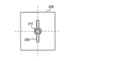
- FIG. 20 shows a structural example of a vertical cavity surface emitting laser which is the light source 130 shown in FIG.
- an n-type DBR (Diffracted Bragg Reflector) layer 201 is formed on an n-type GaAs substrate 200.
- An active layer 202 and an oxidized constricting layer 203 are provided at the center of an n-type DBR (Diffracted Bragg Reflector) layer 201.
- a p-type DBR layer 204 is provided on the oxidized constricting layer 203.
- An electrode 206 is formed on these peripheral portions with an insulating layer 205 interposed therebetween.
- An electrode 207 is also formed on the back side of the n-type GaAs substrate 200.
- FIG. 20 shows a structural example of a vertical cavity surface emitting laser which is the light source 130 shown in FIG.
- an n-type DBR (Diffracted Bragg Reflector) layer 201 is formed on an n-type GaAs substrate 200.
- the active layer 202 is interposed between the n-type DBR layer 201 and the p-type DBR layer 204, and light generated in the active layer 202 is between the n-type DBR layer 201 and the p-type DBR layer 204.
- a vertical resonator 210 that resonates is formed. Note that the vertical cavity surface emitting laser is not limited to the example of FIG. 20, and for example, the oxidized constricting layer 203 may be omitted.
- the light source 130 shown in FIG. 18 is a vertical cavity surface emitting laser (surface in a broad sense) capable of resonating light in a direction perpendicular to the substrate surface and emitting light in a direction perpendicular to the substrate surface (optical axis of the light source).
- a light emitting laser By using a vertical cavity surface emitting laser, a light source that is monochromatic (single wavelength) and linearly polarized can be configured. Further, the vertical cavity surface emitting laser can be miniaturized and is suitable for incorporation into a portable detection device.
- the structure of the vertical cavity surface emitting laser enables the formation of the resonator 210 and the inspection of the laser characteristics without cleaving the substrate in the manufacturing process, which is suitable for mass production.
- the vertical cavity surface emitting laser can be manufactured at a relatively low cost compared to other semiconductor lasers, and for example, a two-dimensional array type vertical cavity surface emitting laser can be provided.
- the threshold current of the vertical cavity surface emitting laser is small, so that the power consumption of the detection device 100 can be reduced.
- the vertical cavity surface emitting laser can be modulated at high speed even with a low current, and the width of the characteristic change with respect to the temperature change of the vertical cavity surface emitting laser is small, and the temperature control unit of the vertical cavity surface emitting laser can be simplified. .
- a distortion applying portion 220 can be disposed adjacent to the resonator 210 shown in FIG.
- the distortion adding unit 220 applies anisotropic stress to the resonator 210 and distorts it, thereby causing the polarization dependency of birefringence and gain in the resonator.
- the flat metal layer 15 shown in FIG. 1 is replaced with an uneven metal layer 15A.
- this structure is the structure disclosed in Japanese Patent Application No. 2011-139526 by the present applicant.
- the irregularity period of the metal layer 15 ⁇ / b> A is, for example, 10 times or more larger than the arrangement period of the metal nanostructures 17.
- surface plasmons can be generated when light enters the concavo-convex portions of the lattice, and propagation plasmons can be enhanced.
- FIG. 23 shows a structure in which the metal nanostructure 17 of FIG. 22 is formed as an Ag metal island on a SiO 2 layer (dielectric layer) 16 having a thickness of 40 nm, for example.
- the surface of the dielectric 16 is flattened in FIG. 22, the uneven pattern of the metal film 15 made of, for example, Au is reflected on the surface of the dielectric 16 without being flattened in FIG. That is, the surface of the dielectric 16 may or may not be planarized.
- the size of the Ag particles shown in FIG. 23 varies in the range of 20 to 80 nm and has no periodicity.
Landscapes
- Health & Medical Sciences (AREA)
- Nuclear Medicine, Radiotherapy & Molecular Imaging (AREA)
- Physics & Mathematics (AREA)
- Life Sciences & Earth Sciences (AREA)
- Chemical & Material Sciences (AREA)
- Analytical Chemistry (AREA)
- Biochemistry (AREA)
- General Health & Medical Sciences (AREA)
- General Physics & Mathematics (AREA)
- Immunology (AREA)
- Pathology (AREA)
- Investigating, Analyzing Materials By Fluorescence Or Luminescence (AREA)
Priority Applications (2)
| Application Number | Priority Date | Filing Date | Title |
|---|---|---|---|
| CN201380022692.3A CN104272090A (zh) | 2012-05-01 | 2013-04-23 | 光学装置以及检测装置 |
| US14/398,078 US20150131092A1 (en) | 2012-05-01 | 2013-04-23 | Optical device and detection apparatus |
Applications Claiming Priority (2)
| Application Number | Priority Date | Filing Date | Title |
|---|---|---|---|
| JP2012-104462 | 2012-05-01 | ||
| JP2012104462A JP5935492B2 (ja) | 2012-05-01 | 2012-05-01 | 光学デバイス及び検出装置 |
Publications (1)
| Publication Number | Publication Date |
|---|---|
| WO2013164904A1 true WO2013164904A1 (ja) | 2013-11-07 |
Family
ID=49514311
Family Applications (1)
| Application Number | Title | Priority Date | Filing Date |
|---|---|---|---|
| PCT/JP2013/002722 WO2013164904A1 (ja) | 2012-05-01 | 2013-04-23 | 光学デバイス及び検出装置 |
Country Status (4)
| Country | Link |
|---|---|
| US (1) | US20150131092A1 (zh) |
| JP (1) | JP5935492B2 (zh) |
| CN (1) | CN104272090A (zh) |
| WO (1) | WO2013164904A1 (zh) |
Families Citing this family (10)
| Publication number | Priority date | Publication date | Assignee | Title |
|---|---|---|---|---|
| JP6201369B2 (ja) * | 2013-03-28 | 2017-09-27 | セイコーエプソン株式会社 | 検出装置及び電子機器 |
| JP6380899B2 (ja) * | 2014-08-29 | 2018-08-29 | 国立研究開発法人物質・材料研究機構 | 電磁波吸収及び輻射材料及びその製造方法並びに赤外線源 |
| JP6613736B2 (ja) * | 2015-09-07 | 2019-12-04 | セイコーエプソン株式会社 | 物質検出方法および物質検出装置 |
| CN108463711A (zh) * | 2015-11-18 | 2018-08-28 | 雷迪奥米特医学公司 | 用于检测全血样品中的游离血红蛋白的光学传感器 |
| TW201725385A (zh) * | 2016-01-05 | 2017-07-16 | 財團法人工業技術研究院 | 具有薄層層析之拉曼檢測晶片及分離檢測分析物之方法 |
| US20190391302A1 (en) * | 2017-01-30 | 2019-12-26 | Aalto University Foundation Sr | A plasmonic device |
| CN111830614A (zh) * | 2020-05-13 | 2020-10-27 | 华南师范大学 | 利用激光偏振态实现纳米光栅刻印的解决方案 |
| KR102501486B1 (ko) * | 2020-12-10 | 2023-02-17 | 한국화학연구원 | 나노 입자 또는 나노 구조체에서 발생된 분광 신호 분석 시스템 및 분석 방법 |
| CN113268866A (zh) * | 2021-05-13 | 2021-08-17 | 国网山东省电力公司电力科学研究院 | 计算电场作用下c5f10o绝缘气体在铜表面吸附的方法 |
| US11959859B2 (en) | 2021-06-02 | 2024-04-16 | Edwin Thomas Carlen | Multi-gas detection system and method |
Citations (2)
| Publication number | Priority date | Publication date | Assignee | Title |
|---|---|---|---|---|
| WO2006132224A1 (ja) * | 2005-06-09 | 2006-12-14 | Tokyo University Of Agriculture And Technology | 反射率変化型センサ、光学式測定装置、反射率変化型センサの製造方法、並びに反射率変化型センサ用自己組織化微粒子単層膜、自己組織化微粒子単層膜及びこれら単層膜の製造方法 |
| JP2011141265A (ja) * | 2009-12-11 | 2011-07-21 | Seiko Epson Corp | センサーチップ、センサーカートリッジ及び分析装置 |
Family Cites Families (8)
| Publication number | Priority date | Publication date | Assignee | Title |
|---|---|---|---|---|
| US8497131B2 (en) * | 1999-10-06 | 2013-07-30 | Becton, Dickinson And Company | Surface enhanced spectroscopy-active composite nanoparticles comprising Raman-active reporter molecules |
| JP5175584B2 (ja) * | 2008-03-13 | 2013-04-03 | 地方独立行政法人 東京都立産業技術研究センター | 局所表面プラズモン共鳴イメージング装置 |
| WO2010001601A1 (ja) * | 2008-07-02 | 2010-01-07 | 株式会社ネクスト21 | カルシウムイオン溶出を制御した人工骨材料 |
| WO2010091293A1 (en) * | 2009-02-06 | 2010-08-12 | The Regents Of The University Of California | Plasmonic system for detecting binding of biological molecules |
| EP2325634B1 (en) * | 2009-11-19 | 2015-03-18 | Seiko Epson Corporation | Sensor chip, sensor cartridge, and analysis apparatus |
| EP2372348A1 (en) * | 2010-03-22 | 2011-10-05 | Imec | Methods and systems for surface enhanced optical detection |
| JP5939016B2 (ja) * | 2012-04-27 | 2016-06-22 | セイコーエプソン株式会社 | 光学デバイス及び検出装置 |
| JP2014119263A (ja) * | 2012-12-13 | 2014-06-30 | Seiko Epson Corp | 光学デバイス、検出装置、電子機器及び光学デバイスの製造方法 |
-
2012
- 2012-05-01 JP JP2012104462A patent/JP5935492B2/ja not_active Expired - Fee Related
-
2013
- 2013-04-23 WO PCT/JP2013/002722 patent/WO2013164904A1/ja active Application Filing
- 2013-04-23 US US14/398,078 patent/US20150131092A1/en not_active Abandoned
- 2013-04-23 CN CN201380022692.3A patent/CN104272090A/zh active Pending
Patent Citations (2)
| Publication number | Priority date | Publication date | Assignee | Title |
|---|---|---|---|---|
| WO2006132224A1 (ja) * | 2005-06-09 | 2006-12-14 | Tokyo University Of Agriculture And Technology | 反射率変化型センサ、光学式測定装置、反射率変化型センサの製造方法、並びに反射率変化型センサ用自己組織化微粒子単層膜、自己組織化微粒子単層膜及びこれら単層膜の製造方法 |
| JP2011141265A (ja) * | 2009-12-11 | 2011-07-21 | Seiko Epson Corp | センサーチップ、センサーカートリッジ及び分析装置 |
Also Published As
| Publication number | Publication date |
|---|---|
| CN104272090A (zh) | 2015-01-07 |
| JP2013231686A (ja) | 2013-11-14 |
| JP5935492B2 (ja) | 2016-06-15 |
| US20150131092A1 (en) | 2015-05-14 |
Similar Documents
| Publication | Publication Date | Title |
|---|---|---|
| JP5935492B2 (ja) | 光学デバイス及び検出装置 | |
| JP5939016B2 (ja) | 光学デバイス及び検出装置 | |
| US8877519B2 (en) | Chemical sensor element, sensing apparatus, and sensing method | |
| Brolo et al. | Nanohole-enhanced Raman scattering | |
| JP5609241B2 (ja) | 分光方法及び分析装置 | |
| JP5545144B2 (ja) | 光デバイスユニット及び検出装置 | |
| JP2014119263A (ja) | 光学デバイス、検出装置、電子機器及び光学デバイスの製造方法 | |
| Lis et al. | Localized surface plasmon resonances in nanostructures to enhance nonlinear vibrational spectroscopies: towards an astonishing molecular sensitivity | |
| US10996172B2 (en) | Surface-functionalized nanostructures for molecular sensing applications | |
| JP2015212626A (ja) | 電場増強素子、ラマン分光法、ラマン分光装置、および電子機器 | |
| JP2013096939A (ja) | 光デバイス及び検出装置 | |
| Canpean et al. | Multifunctional plasmonic sensors on low-cost subwavelength metallic nanoholes arrays | |
| JP2016003946A (ja) | 電場増強素子、分析装置、及び電子機器 | |
| JP6418379B2 (ja) | 電場増強素子、ラマン分光装置、および電子機器 | |
| JP2013246115A (ja) | 光学デバイス及び検出装置 | |
| US20150212004A1 (en) | Electric field enhancement element, raman spectroscopic method, raman spectroscopic device, and electronic apparatus | |
| US20160223466A1 (en) | Electric-field enhancement element, analysis device, and electronic apparatus | |
| JP2015141068A (ja) | ラマン分光装置、及び電子機器 | |
| JP2013231685A (ja) | 検出装置 | |
| JP6586867B2 (ja) | 電場増強素子およびラマン分光装置 | |
| JP2015096813A (ja) | ラマン分光装置、及び電子機器 | |
| JP2016004018A (ja) | ラマン分光装置および電子機器 | |
| JP2017211395A (ja) | ラマン分光装置、ラマン分光法、および電子機器 | |
| Laible et al. | 3.1 Localized surface plasmon resonance shift sensing | |
| Wei et al. | A study of localized surface plasmon resonance nanoslit array and applications for chip-based protein detection |
Legal Events
| Date | Code | Title | Description |
|---|---|---|---|
| 121 | Ep: the epo has been informed by wipo that ep was designated in this application |
Ref document number: 13785113 Country of ref document: EP Kind code of ref document: A1 |
|
| WWE | Wipo information: entry into national phase |
Ref document number: 14398078 Country of ref document: US |
|
| NENP | Non-entry into the national phase |
Ref country code: DE |
|
| 122 | Ep: pct application non-entry in european phase |
Ref document number: 13785113 Country of ref document: EP Kind code of ref document: A1 |