WO2013164904A1 - Optical device and detecting apparatus - Google Patents
Optical device and detecting apparatus Download PDFInfo
- Publication number
- WO2013164904A1 WO2013164904A1 PCT/JP2013/002722 JP2013002722W WO2013164904A1 WO 2013164904 A1 WO2013164904 A1 WO 2013164904A1 JP 2013002722 W JP2013002722 W JP 2013002722W WO 2013164904 A1 WO2013164904 A1 WO 2013164904A1
- Authority
- WO
- WIPO (PCT)
- Prior art keywords
- light
- film
- organic molecular
- optical device
- metal
- Prior art date
Links
Images


Classifications
-
- G—PHYSICS
- G01—MEASURING; TESTING
- G01N—INVESTIGATING OR ANALYSING MATERIALS BY DETERMINING THEIR CHEMICAL OR PHYSICAL PROPERTIES
- G01N21/00—Investigating or analysing materials by the use of optical means, i.e. using sub-millimetre waves, infrared, visible or ultraviolet light
- G01N21/62—Systems in which the material investigated is excited whereby it emits light or causes a change in wavelength of the incident light
- G01N21/63—Systems in which the material investigated is excited whereby it emits light or causes a change in wavelength of the incident light optically excited
- G01N21/65—Raman scattering
- G01N21/658—Raman scattering enhancement Raman, e.g. surface plasmons
-
- G—PHYSICS
- G01—MEASURING; TESTING
- G01N—INVESTIGATING OR ANALYSING MATERIALS BY DETERMINING THEIR CHEMICAL OR PHYSICAL PROPERTIES
- G01N2201/00—Features of devices classified in G01N21/00
- G01N2201/06—Illumination; Optics
- G01N2201/061—Sources
- G01N2201/06113—Coherent sources; lasers
Definitions
- the present invention relates to an optical device, a detection apparatus, and the like.
- surface plasmon is a vibration mode of an electron wave that causes coupling with light due to boundary conditions unique to the surface.
- a method of exciting surface plasmons there are a method of engraving a diffraction grating on a metal surface and combining light and plasmons and a method of using evanescent waves.
- a sensor using SPR includes a total reflection prism and a metal film that contacts a target substance formed on the surface of the prism. With such a configuration, the presence or absence of target substance adsorption, such as the presence or absence of antigen adsorption in an antigen-antibody reaction, is detected.
- the Raman scattering light is irradiated to the enhanced electric field formed by localized surface plasmon resonance (LSPR) using metal nanostructures (LSPR), the Raman scattering light is enhanced by the surface enhanced Raman scattering phenomenon.
- LSPR localized surface plasmon resonance
- LSPR metal nanostructures
- Patent Document 1 a self-assembled monolayer (SAM) is formed on a metal surface of a sensor chip.
- SAM self-assembled monolayer
- Patent Document 2 proposes to form a mixture of different types of SAM films.
- this type of detection apparatus is excellent in that it can detect a sample to be measured having an extremely low concentration, but it is expected that the concentration range to be detected is wide depending on the sample to be measured. However, there is a limit in detecting a measurement sample having a wide concentration range even if the measurement target has a relatively low concentration, and the SERS signal level is saturated.
- some aspects of the present invention have an object to provide an optical device and a detection apparatus that can detect a sample to be measured in a wide range of concentrations even if the object to be measured has a relatively low concentration. .
- One aspect of the present invention is An optical device that emits light for detecting and / or identifying a sample to be measured when excitation light is incident thereon, A plurality of metal nanostructures formed on a dielectric; A first organic molecular film formed on the dielectric between two adjacent metal nanostructures of the plurality of metal nanostructures; A second organic molecular film different from the first organic molecular film formed in the plurality of metal nanostructures, The first organic molecular film and the second organic molecular film relate to an optical device that attaches (captures) the sample to be measured.
- an enhanced electric field is formed between the metal nanostructures to form a hot spot.
- the enhanced electric field in the region facing the metal nanostructure is not as strong as the enhanced electric field between the metal nanostructures. Therefore, focusing on the fact that the enhanced electric field differs between the region of the metal nanostructure and the region between the metal nanostructures, detection was attempted in a wide concentration range from low concentration to high concentration.
- the metal nanostructure has a low desorption activation energy that keeps the sample to be measured in the adsorbed state, the desorption activation energy is overcome by thermal energy at about room temperature, and the sample to be measured is desorbed.
- the first and second organic molecular films a desorption activation energy larger than the desorption activation energy by only the metal nanostructure is secured, and desorption of the sample to be measured can be suppressed. Thereby, a detection signal level can be raised.
- the concentration range from a low concentration to a high concentration can be obtained.
- the detection sensitivity can be adjusted appropriately.
- the metal nanostructures on which the first organic molecular film is formed is a hot spot with a strong enhanced electric field, and even a low-measurement sample can be detected with high sensitivity.
- the region of the metal nanostructure where the second organic molecular film is formed has a relatively weak enhanced electric field, but if the sample to be measured has a high concentration, the signal level based on the detection light is reflected on the light reflecting the sample to be measured. Secured. Therefore, the formation region of the first molecular film becomes a first detection region for detecting a low concentration sample to be measured, and the formation region of the second organic molecular film becomes a second detection region for detecting a high concentration sample to be measured. Can do.
- the concentration range of the sample to be measured that can be detected by one detection device is expanded. Then, by selecting the first and second organic molecular films, a sample to be measured having a concentration range in which the signal level based on the light detected by the first detection unit on which the first organic film is formed is saturated is selected. It can be detected by the second detection unit on which two organic molecular films are formed.
- the first organic molecular film has a silane coupling agent, a silanol group (—Si—OH), a titanium coupling agent), or a titanol group (—Ti—OH). Can do.
- the organic molecular film having these groups is suitable as the first organic molecular film because it is easily adsorbed on a dielectric such as SiO 2 .
- the silane coupling agent or the titanium coupling agent generates a silanol group (—Si—OH) or a titanol group (—Ti—OH) bonded to the OH group of the dielectric by hydrolysis or the like. .
- An organic molecular film having these groups is suitable as a second organic molecular film because it is easily adsorbed to a metal.
- the second organic molecular film may have a thiol group (—SH), a disulfide group (—S—S—), or a carboxyl group (—COOH).
- the molecular length of the first organic molecular film can be shorter than the molecular length of the second organic molecular film.
- the molecular length of the organic molecular film is preferably matched to the magnitude of the enhanced electric field in the region where the organic molecular film is formed. Since the enhanced electric field is formed in a wide range in the region of the metal nanostructure, the second organic molecular film having a long molecular length is selected, and the enhanced electric field is formed in a narrow range between the metal nanostructures, so the molecular length is short.
- the first organic molecular film can be selected.
- Another aspect of the present invention is: A light source; Any one of the optical devices (1) to (4) into which light from the light source is incident; A photodetector for detecting light emitted from the optical device; It is related with the detection apparatus which has.
- This detection device can detect a sample to be measured with an increased sensitivity in a concentration range from a low concentration to a high concentration.
- FIGS. 2A to 2D are explanatory diagrams of the principle of detection of surface-enhanced Raman light. It is a figure which shows the intermediate substrate in which the 2nd organic molecular film was formed in the basic structure of FIG. It is a figure which shows the optical device which concerns on 1st Embodiment of this invention by which the 1st organic molecular film was formed in the intermediate substrate of FIG. It is a figure which shows the result of having measured the SERS signal acquired by exposing various saturated vapor gases, and the adsorption amount of various saturated vapor gases.
- FIG. 1 It is a figure which shows the whole structure of the detection apparatus which concerns on 4th Embodiment of this invention. It is a control system block diagram of the detection apparatus shown in FIG. It is a figure which shows the light source of the detection apparatus shown in FIG. It is a figure which shows the two resonators and distortion addition part which were provided in the light source shown in FIG. It is a figure which shows the modification of the basic structure of the optical device shown in FIG. It is a figure which shows the optical device which made the metal nanostructure Ag island.
- FIG. 1 shows a basic substrate 10 that is a basic structure of an optical device 12 according to the first embodiment.
- the optical device 12 according to the first embodiment is based on the basic substrate 10 shown in FIG. 1, and passes through the intermediate substrate 11 on which the second organic molecular film 19 shown in FIG. 3 is formed, for example, as shown in FIG. First and second organic molecular films 18 and 19 are formed on the basic substrate 10A to complete. First, the basic substrate 10 will be described.
- the basic substrate 10 shown in FIG. 1 includes a substrate 14, a metal (conductor) film 15 formed on the substrate 14, and a dielectric 16 formed on the metal film 15. And the metal nanostructure 17 formed on the dielectric 16.
- the metal nanostructure 17 may be a one-dimensional array or a two-dimensional array.
- the metal nanostructure 17 is a nano-order metal nanoparticle smaller than the wavelength of incident light and has a size of 1 to 1000 nm.
- Examples of the metal nanostructure 17 include gold (Au), silver (Ag), copper (Cu), aluminum (Al), palladium (Pd), nickel (Ni), platinum (Pt), molybdenum (Mo), chromium ( Cr) or an alloy or composite of these is used.
- the metal nanostructure 17 may be formed so as to cover the convex portion of the dielectric 16 (see FIG. 2D).
- the metal film 15 is formed as a propagation type plasmon enhancement structure, and a flat film (FIG. 1) or a metal diffraction grating with periodic unevenness (see FIGS. 22 and 23 described later) is suitable.
- FIG. 1 shows an example in which a gold (Au) metal film 15 is formed by vacuum deposition or sputtering.
- the thickness of the Au film is preferably about 10 nm to several tens of nm.
- the types of metals are gold (Au), silver (Ag), copper (Cu), aluminum (Al), platinum (Pt), nickel (Ni), palladium (Pd), tungsten (W), rhodium (Rh). Ruthenium (Ru) is suitable.
- the dielectric 16 SiO 2 , Al 2 O 3 , TiO 2 or the like is suitable, and the thickness is desirably about 10 nm to 500 nm.
- FIG. 2A to FIG. 2D are explanatory diagrams of the detection principle of Raman scattered light as an example of the light detection principle reflecting a fluid sample.
- incident light frequency ⁇
- sample molecule sample molecule 1 adsorbed on the optical device 12.
- most of the incident light is scattered as Rayleigh scattered light, and the frequency ⁇ or wavelength of the Rayleigh scattered light does not change with respect to the incident light.
- a part of the incident light is scattered as Raman scattered light, and the frequency ( ⁇ ′ and ⁇ + ⁇ ′) or wavelength of the Raman scattered light reflects the frequency ⁇ ′ (molecular vibration) of the sample molecule 1.
- the Raman scattered light is light reflecting the sample molecule 1 to be inspected.
- a part of the incident light causes the sample molecule 1 to vibrate and loses energy, but the vibration energy of the sample molecule 1 may be added to the vibration energy or light energy of the Raman scattered light.
- Such a frequency shift ( ⁇ ′) is called a Raman shift.
- FIG. 2 (B) shows an example of acetaldehyde as a fingerprint spectrum unique to the target molecule.
- the detected substance can be identified as acetaldehyde.
- the Raman scattered light is very weak and it is difficult to detect a substance that exists only in a trace amount.
- an enhanced electric field 13 is formed in a gap between adjacent metal nanostructures 17 in a region where incident light is incident.
- the electric field of the incident light is free on the surface of the metal nanostructure 17. Acts on electrons and causes resonance. As a result, electric dipoles due to free electrons are excited in the metal nanostructure 17, and an enhanced electric field 13 stronger than the electric field of incident light is formed. This is also called Localized Surface Plasmon Resonance (LSPR). This phenomenon is a phenomenon peculiar to metal grains having convex portions of 1 to 1000 nm smaller than the wavelength of incident light.
- LSPR Localized Surface Plasmon Resonance
- the propagation surface plasmon can be formed by a propagation structure formed by the metal film 15.
- the propagation surface plasmon can be formed by a propagation structure formed by the metal film 15.
- the metal film 15 has an uneven lattice surface
- surface plasmon is generated when light enters the uneven surface of the lattice. If the polarization direction of the incident light is orthogonal to the groove direction of the grating, the vibration of the electromagnetic wave is excited with the vibration of free electrons in the metal grating. Since the vibration of the electromagnetic wave affects the vibration of free electrons, surface plasmon polariton, which is a system in which both vibrations are combined, is formed. However, propagation surface plasmons are generated even if the metal film 15 is flat. The surface plasmon polariton propagates along the interface between the metal film 15 and the dielectric 16 and further enhances the enhanced electric field 13.
- the finished optical device 12 has a first organic molecular film 18 and a second organic molecular film 19 on the surface, as shown in FIG. .
- the first and second organic molecular films 18 and 19 are adsorption films that capture molecules that are fluid samples, and are formed of, for example, a self-assembled monomolecular film (SAM).
- SAM self-assembled monomolecular film
- the first and second organic molecular films 18 and 19 are formed of different SAM films.
- the first organic molecular film 18 is formed on the dielectric 16 between two adjacent metal nanostructures 17.
- the second organic molecular film 19 is formed on the metal nanostructure 17.
- the second organic molecular film 19 is first formed as shown in FIG. 3, and then the first organic molecular film 18 is formed as shown in FIG. However, it is not limited to this order.
- the target molecule In order to detect the SERS signal described with reference to FIGS. 2A to 2D, it is necessary that the target molecule be adsorbed on the surface of the optical device 12. Silver (Ag), gold (Au), platinum (Pt), etc. have been reported as metals that have a large effect of plasmon resonance among metals, but all target molecules are adsorbable with these metals. It ’s not good. Even if the metal is once adsorbed, if the desorption activation energy Ed is small, it is desorbed immediately by thermal energy at about room temperature, and a SERS signal cannot be obtained.
- FIG. 5 shows the results of exposure of various saturated vapor gases to a substrate in which an Ag nanostructure is formed as a metal nanostructure on a quartz glass substrate.
- the SERS signal is detected when the amount of water remaining after exposure to the atmosphere is large (the gas in the right region in FIG. 5).
- FIG. 5 also shows the results of measuring the amount of adsorption from the change in the frequency of the crystal resonator by exposing various saturated vapor gases to the thickness vibration type crystal resonator (QCM).
- QCM thickness vibration type crystal resonator
- the value when exposed to saturated vapor gas is set to 1, and the amount remaining after switching to atmospheric exposure is expressed as a ratio.
- the gas in which the SERS signal is not detected is almost adsorbed on the surface of the crystal unit (Au) and is immediately desorbed, and the gas in which the SERS signal is detected is adsorbed to the surface of the crystal unit (Au) to some extent. It is done.
- the desorption rate v (t) of the adsorbed gas is expressed as follows from the Polanyi-Wigner equation.
- v (t) is the desorption rate
- ⁇ (t) is the coverage
- C is the gas adsorption amount
- ⁇ n is the frequency factor
- n is the reaction order
- Ed is the desorption activation energy
- R is the gas constant
- the desorption remaining amount ⁇ (t) is expressed as follows by integrating the desorption rate v (t).
- the desorption activation energy Ed can be measured by measuring the change in mass of the molecules adsorbed on the surface of the QCM (quartz crystal) as the change in frequency. That is, the desorption activation energy Ed can be measured as a frequency change in the curve A region of FIG.
- the desorption activation energy Ed may be made larger than that of the metal nanostructure forming the enhanced electric field. For this reason, it can be predicted that this can be realized by surface-treating the metal nanostructure.
- a surface treatment that allows gas molecules to fall within the range of the enhanced electric field created by the metal nanostructure is desired. Even if spin coating is performed by dissolving a normal resin-based material in a solvent, the thickness becomes approximately several tens of nanometers, so that it is out of the strong electric field range and it is difficult to obtain a strong surface-enhanced Raman effect. .
- the desorption activation energy is improved by an organic molecular film such as a self-assembled monomolecular film (SAM film).
- an organic molecular film such as a self-assembled monomolecular film (SAM film).
- FIG. 9 shows the result of obtaining the desorption activation energy from the temporal change of the remaining amount of desorption (adsorption amount) by forming a SAM film on the crystal resonator (Au electrode).
- the numerical values in FIG. 9 are in units of kJ / mol, measured three times for one sample, and the average value thereof was adopted.
- PEG in FIG. 9 is polyethylene glycol.
- the desorption activation energy is greater when the SAM film is present than when the SAM film is absent except for acetic acid.
- pyridinethiol has a relatively short molecular length
- PEG thiol and hexadecanethiol have a relatively long molecular length.
- a fluid sample can be detected in a wide concentration range as shown in FIG. This is realized by changing the types of organic molecular films 18 and 19 formed in the enhanced electric field having different strengths.
- a strong enhanced electric field 13 is formed between the metal nanostructures 17 as described above and becomes a hot spot.
- the enhanced electric field in the region facing the metal nanostructure 17 is not as strong as the enhanced electric field between the metal nanostructures 17.
- the first and second organic molecular films 18 and 19 ensure a desorption activation energy larger than the desorption activation energy of the metal nanostructure 17 alone, and can suppress desorption of the sample to be measured. Thereby, a detection signal level can be raised.
- the intensity of the SERS signal based on the Raman scattered light in the region between the metal nanostructures 17 where the first organic molecular film 18 is formed is indicated by the broken line with the “adsorption film 1” attached. As shown in FIG.
- the region of the metal nanostructure 17 where the second organic molecular film 19 is formed has a relatively weak enhanced electric field.
- the second organic molecule 19 improves the adsorptivity of the sample to be measured, As long as it is a measurement sample, the signal level based on the detection light is ensured for the light reflecting the sample to be measured. Therefore, as shown in FIG. 10, the intensity of the SERS signal based on the Raman scattered light in the region of the metal nanostructure 17 where the second organic molecular film 19 is formed is as shown by the broken line with the “adsorption film 2” attached. Furthermore, it changes in the high concentration region.
- the concentration range of the sample to be measured that can be detected by one detection device is expanded.
- the SERS signal level based on the Raman scattered light from the formation region of the first organic molecular film 18 is saturated as shown by the broken line labeled “Adsorption film 1” in FIG. Therefore, by selecting the first and second organic molecular films 18 and 19, from the concentration range where the SERS signal level shown by “adsorption film 1” shown in FIG. 10 is saturated, from the formation region of the second organic molecular film 19. It is possible to adjust so that the SERS signal level (broken line with “adsorption film 2”) based on the Raman scattered light is detected.
- the signal level obtained by adding the two broken line levels labeled “Adsorption film 1” and “Adsorption film 2” in FIG. 10 is the output from the photodetector.
- the output from the photodetector can be changed with a constant inclination as indicated by a solid line with “adsorption film 1 + adsorption film 2” in FIG.
- the second organic molecular film (second SAM film) 19 shown in FIG. 3 can be formed by the liquid phase method of FIG. In FIG. 11, a basic substrate 10 having the basic structure of the optical device 10 shown in FIG. 1 is immersed in a container 41 in which a liquid SAM film material 40 is accommodated. Since the thiol group of the second SAM film 19 is easily adsorbed to the metal nanostructure 17 and the alkyl groups in the molecular structure act so as to maintain a certain distance from each other by van der Waals force. The film 19 is adsorbed so as to be arranged on the metal nanostructure 17.
- the liquid SAM film material 40 does not enter the valleys of the metal nanostructure 17 due to the surface tension.
- the second SAM film 19 is formed only on the metal nanostructure 17.
- the type of SAM film having a molecular length suitable for the enhanced electric field near the surface is selected.
- the enhanced electric field due to the enhanced structure covers a relatively wide range, and the second SAM film 19 having a relatively long molecular length suitable for the wide enhanced electric field is formed by the liquid phase method.
- the second SAM film 19 11-mercapto-1-undecanol, 11-mercaptoundecanoic acid, PEG3-OH alkanethiol or Hydroxy-EG3-undecanethiol, Thiol-dPEG4-acid, hexadecanethiol, propanethiol, 4-mercaptopyridine, thionicotinic acid
- a SAM film having a molecular length suitable for an enhanced electric field, such as a silane coupling agent, is selected, but is not limited to the above examples.
- a film having a thiol group (—SH), a disulfide group (—S—S—), and a carboxyl group (—COOH) is suitable.
- a thiol reagent having an alkyl chain or a PEG chain and having a functional group such as OH or COOH at the terminal can be used as the second SAM film 19.
- the first organic molecular film (first SAM film) 18 shown in FIG. 4 is formed by the vapor phase method of FIG. 13 or FIG.
- any SAM film material can be used as long as evaporation and sublimation are possible, and the valley of the metal nanostructure 17 shown in FIG.
- FIG. 4 shows an example of thionicotinic acid as the first SAM film 18, it is not limited to this.
- the optical device 12 shown in FIG. 4 can be completed through the intermediate substrate 11 shown in FIG.
- the gas phase method of FIG. 13 shows a case where the material of the SAM film is a liquid.
- a small amount of the liquid SAM film material 43 is put into the container 42 to evaporate, and the SAM film material 44 converted into a gas is
- the metal nanostructures 17 of the intermediate substrate 11 placed in the openings enter and adhere to each other.
- the SAM film material 48 is solid or powder
- the SAM film material 48 accommodated in the bottom of the container 46 is heated and sublimated by the heating device 47 to become a gas.
- the SAM film material 49 enters and adheres between the metal nanostructures 17 of the intermediate substrate 11 placed in the opening of the container 44.
- the first SAM film 18 formed on the dielectric 16 between the metal nanostructures 17 has a silane coupling agent, a silanol group (—Si—OH), a titanium coupling agent, and a titanol group (—Ti—OH). Those are preferred.
- the SERS chip is formed by forming 11-mercapto-1-undecanol as the second SAM film 19 on the metal nanostructure 17 and thionicotinic acid as the first SAM film 18 between the metal nanostructures 17.
- 11-mercapto-1-undecanol as the second SAM film 19 on the metal nanostructure 17
- thionicotinic acid as the first SAM film 18 between the metal nanostructures 17.
- thionicotinic acid was formed as the first SAM film 18 by a vapor phase method.
- the FT-IR spectrum is shown in FIG. 16, and the SERS signal intensity is shown in FIG.
- the electric field enhancement is particularly strong in the valleys between the metal nanostructures 17. Therefore, when a target molecule exists in this valley, information on the target molecule is obtained as a signal.
- FIG. 17 indicates that no SAM-derived signal could be observed before the formation of the thionicotinic acid SAM as the first SAM film 18 (that is, the formation of only the second SAM, 11-mercapto-1-undecanol SAM).
- the chip after the formation of thionicotinic acid SAM only a signal derived from thionicotinic acid indicated by an arrow in FIG. 17 was observed. From this result, it can be seen that only the thionicotinic acid SAM was formed in the valleys between the metal nanostructures 17 and the 11-mercapto-1-undecanol SAM was formed only at the top of the metal nanostructures 17.
- FIG. 18 shows a specific configuration example of the detection apparatus of the present embodiment.
- 18 includes a sample supply channel 101 having a suction port 101A and a dust removal filter 101B, a sample discharge channel 102 having a discharge port 102A, and an optical device (sensor chip) 103 having the structure shown in FIG. And the like.
- Light is incident on the optical device 103.
- the casing 120 of the detection apparatus 100 includes a sensor cover 122 that can be opened and closed by a hinge part 121.
- the optical device unit 110 is detachably arranged with respect to the housing 120 in the sensor cover 122. Whether the optical device unit 110 is mounted / not mounted can be detected by the sensor detector 123.
- the sample supply flow channel 101 and the sample discharge flow channel 102 are formed so as to be detoured, so that external light is not easily incident.
- the shape of the path for sucking and discharging the fluid sample is considered so that light from the outside does not enter the sensor and the fluid resistance to the fluid sample is reduced. By preventing external light from entering the optical device 103, light that becomes noise other than Raman scattered light does not enter, and the S / N ratio of the signal is improved.
- the shape of the flow path is made smooth by eliminating the corners as much as possible, so that the stay at the corners is eliminated.
- the negative pressure generating unit 103 provided in the fluid discharge channel 102 it is also necessary to select a fan or a pump having a static pressure and an air volume corresponding to the channel resistance.
- a light source 130 In the housing 120, a light source 130, an optical system 131, a light detection unit 132, a signal processing / control unit 133, and a power supply unit 134 are provided.
- the light source 130 is, for example, a laser, and a vertical cavity surface emitting laser can be preferably used from the viewpoint of miniaturization, but is not limited thereto.
- the light from the light source 130 is collimated by a collimator lens 131A constituting the optical system 131.
- a polarization control element may be provided downstream of the collimator lens 131A and converted to linearly polarized light. However, if, for example, a surface emitting laser is used as the light source 130 and light having linearly polarized light can be emitted, the polarization control element can be omitted.
- the light collimated by the collimator lens 131A is guided in the direction of the optical device 103 by the half mirror (dichroic mirror) 131B, is condensed by the objective lens 131C, and enters the optical device 103.
- Rayleigh scattered light and Raman scattered light from the optical device 103 pass through the objective lens 131C and are guided toward the light detection unit 100 by the half mirror 131B.
- Rayleigh scattered light and Raman scattered light from the optical device 103 are collected by the condenser lens 131D and input to the light detection unit 132.
- the light detection unit 132 reaches the optical filter 132A.
- Raman scattered light is extracted by the optical filter 132A (for example, a notch filter).
- This Raman scattered light is further received by the light receiving element 132C via the spectroscope 132B.
- the spectroscope 132B is formed of, for example, an etalon using Fabry-Perot resonance, and the pass wavelength band can be made variable.
- the wavelength of the light passing through the spectroscope 132B can be controlled (selected) by the signal processing / control circuit 133.
- a Raman spectrum peculiar to the sample molecule 1 is obtained by the light receiving element 132C, and the sample molecule 1 can be specified by collating the obtained Raman spectrum with previously stored data.
- the power supply unit 134 supplies the power from the power supply connection unit 135 to the light source 130, the light detection unit 132, the signal processing / control unit 133, the fan 104, and the like.
- the power supply unit 134 can be configured by, for example, a secondary battery, and may be configured by a primary battery, an AC adapter, or the like.
- the communication connection unit 136 is connected to the signal processing / control unit 133 and mediates data, control signals, and the like to the signal processing / control unit 133.
- the signal processing / control unit 133 can send a command to the light detection unit 132, the fan 104, etc. other than the light source 130 shown in FIG. Furthermore, the signal processing / control unit 1330 can execute spectroscopic analysis using a Raman spectrum, and the signal processing / control unit 133 can specify the sample molecule 1.
- the signal processing / control unit 133 can transmit the detection result by Raman scattered light, the spectroscopic analysis result by Raman spectrum, and the like to an external device (not shown) connected to the communication connection unit 136, for example.
- FIG. 19 is a control system block diagram of the detection apparatus 100 of FIG. As illustrated in FIG. 19, the detection apparatus 100 may further include, for example, an interface 140, a display unit 150, an operation panel 160, and the like. 19 may include, for example, a CPU (Central Processing Unit) 133A, a RAM (Random Access Memory) 133B, a ROM (Read Only Memory) 133C, and the like as the control unit.
- a CPU Central Processing Unit
- RAM Random Access Memory
- ROM Read Only Memory
- the detection apparatus 100 can include a light source drive circuit 130A, a spectrum 32B1, a sensor detection circuit 123A, a light receiving circuit 132C1, a fan drive circuit 104A, and the like that drive each unit shown in FIG.
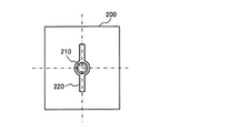
- FIG. 20 shows a structural example of a vertical cavity surface emitting laser which is the light source 130 shown in FIG.
- an n-type DBR (Diffracted Bragg Reflector) layer 201 is formed on an n-type GaAs substrate 200.
- An active layer 202 and an oxidized constricting layer 203 are provided at the center of an n-type DBR (Diffracted Bragg Reflector) layer 201.
- a p-type DBR layer 204 is provided on the oxidized constricting layer 203.
- An electrode 206 is formed on these peripheral portions with an insulating layer 205 interposed therebetween.
- An electrode 207 is also formed on the back side of the n-type GaAs substrate 200.
- FIG. 20 shows a structural example of a vertical cavity surface emitting laser which is the light source 130 shown in FIG.
- an n-type DBR (Diffracted Bragg Reflector) layer 201 is formed on an n-type GaAs substrate 200.
- the active layer 202 is interposed between the n-type DBR layer 201 and the p-type DBR layer 204, and light generated in the active layer 202 is between the n-type DBR layer 201 and the p-type DBR layer 204.
- a vertical resonator 210 that resonates is formed. Note that the vertical cavity surface emitting laser is not limited to the example of FIG. 20, and for example, the oxidized constricting layer 203 may be omitted.
- the light source 130 shown in FIG. 18 is a vertical cavity surface emitting laser (surface in a broad sense) capable of resonating light in a direction perpendicular to the substrate surface and emitting light in a direction perpendicular to the substrate surface (optical axis of the light source).
- a light emitting laser By using a vertical cavity surface emitting laser, a light source that is monochromatic (single wavelength) and linearly polarized can be configured. Further, the vertical cavity surface emitting laser can be miniaturized and is suitable for incorporation into a portable detection device.
- the structure of the vertical cavity surface emitting laser enables the formation of the resonator 210 and the inspection of the laser characteristics without cleaving the substrate in the manufacturing process, which is suitable for mass production.
- the vertical cavity surface emitting laser can be manufactured at a relatively low cost compared to other semiconductor lasers, and for example, a two-dimensional array type vertical cavity surface emitting laser can be provided.
- the threshold current of the vertical cavity surface emitting laser is small, so that the power consumption of the detection device 100 can be reduced.
- the vertical cavity surface emitting laser can be modulated at high speed even with a low current, and the width of the characteristic change with respect to the temperature change of the vertical cavity surface emitting laser is small, and the temperature control unit of the vertical cavity surface emitting laser can be simplified. .
- a distortion applying portion 220 can be disposed adjacent to the resonator 210 shown in FIG.
- the distortion adding unit 220 applies anisotropic stress to the resonator 210 and distorts it, thereby causing the polarization dependency of birefringence and gain in the resonator.
- the flat metal layer 15 shown in FIG. 1 is replaced with an uneven metal layer 15A.
- this structure is the structure disclosed in Japanese Patent Application No. 2011-139526 by the present applicant.
- the irregularity period of the metal layer 15 ⁇ / b> A is, for example, 10 times or more larger than the arrangement period of the metal nanostructures 17.
- surface plasmons can be generated when light enters the concavo-convex portions of the lattice, and propagation plasmons can be enhanced.
- FIG. 23 shows a structure in which the metal nanostructure 17 of FIG. 22 is formed as an Ag metal island on a SiO 2 layer (dielectric layer) 16 having a thickness of 40 nm, for example.
- the surface of the dielectric 16 is flattened in FIG. 22, the uneven pattern of the metal film 15 made of, for example, Au is reflected on the surface of the dielectric 16 without being flattened in FIG. That is, the surface of the dielectric 16 may or may not be planarized.
- the size of the Ag particles shown in FIG. 23 varies in the range of 20 to 80 nm and has no periodicity.
Abstract
Provided are: an optical device which can detect a measurement sample over a wide concentration range, said measurement sample including even a measuring object having a relatively low concentration; and a detecting apparatus. A light from a light source is made to enter an optical device (12), whereby the optical device (12) emits a light which can detect and/or identify a measurement sample. This optical device (12) comprises: multiple metal nanostructures (17) formed on a dielectric body (16); first organic molecule films (18) which are each formed on the dielectric body between two adjacent metal nanostructures; and second organic molecule films (19) which are formed on the multiple metal nanostructures (17) and which are different from the first organic molecule films (18). The first and second organic molecule films adsorb (capture) a measurement sample (1).
Description
本発明は、光学デバイス及び検出装置等に関する。
The present invention relates to an optical device, a detection apparatus, and the like.
近年、医療診断や飲食物の検査等に用いられるセンサーチップの需要が増大しており、高感度かつ小型のセンサーチッブの開発が求められている。このような要求に応えるために、電気化学的な手法をはじめ様々なタイプのセンサーチップが検討されている。これらの中で、集積化が可能であること、低コスト、測定環境を選ばないこと等の理由から、表面プラズモン共鳴(SPR: Surface Plasmon Resonance)を利用した分光分析、特に表面増強ラマン散乱分光(SERS: Surface Enhanced Raman Scattering)用いたセンサーチップに対する関心が高まっている。
In recent years, the demand for sensor chips used for medical diagnosis and inspection of foods and drinks has increased, and the development of highly sensitive and small sensor chips has been demanded. In order to meet such demands, various types of sensor chips including an electrochemical method have been studied. Among these, spectroscopic analysis using surface plasmon resonance (SPR: Surface Plasmon Resonance), especially surface-enhanced Raman scattering spectroscopy (SPR) for reasons such as integration, low cost, and choice of measurement environment Interest in sensor chips using SERS: (Surface (Enhanced (Raman) (Scattering)) is growing.
ここで、表面プラズモンとは、表面固有の境界条件により光とカップリングを起こす電子波の振動モードである。表面プラズモンを励起する方法としては、金属表面に回折格子を刻み、光とプラズモンを結合させる方法やエバネッセント波を利用する方法がある。例えば、SPRを利用したセンサーとしては、全反射型プリズムと、当該プリズムの表面に形成された標的物質に接触する金属膜と、を具備して構成されるものがある。このような構成により、抗原抗体反応における抗原の吸着の有無など、標的物質の吸着の有無を検出している。
Here, surface plasmon is a vibration mode of an electron wave that causes coupling with light due to boundary conditions unique to the surface. As a method of exciting surface plasmons, there are a method of engraving a diffraction grating on a metal surface and combining light and plasmons and a method of using evanescent waves. For example, a sensor using SPR includes a total reflection prism and a metal film that contacts a target substance formed on the surface of the prism. With such a configuration, the presence or absence of target substance adsorption, such as the presence or absence of antigen adsorption in an antigen-antibody reaction, is detected.
ところで、金属表面に伝搬型の表面プラズモンが存在する一方、金属ナノ構造には局在型の表面プラズモンが存在する。局在型の表面プラズモン、つまり、表面の金属ナノ構造上に局在する表面プラズモンが励起された際には、著しく増強された電場が誘起されることが知られている。
By the way, while propagation-type surface plasmons exist on the metal surface, localized-type surface plasmons exist in the metal nanostructure. It is known that when a localized surface plasmon, that is, a surface plasmon localized on a metal nanostructure on the surface is excited, a significantly enhanced electric field is induced.
更に、金属ナノ構造を用いた局在表面プラズモン共鳴(LSPR:Localized Surface Plasmon Resonance)によって形成される増強電場にラマン散乱光が照射されると表面増強ラマン散乱現象によってラマン散乱光が増強されることが知られており、高感度のセンサー(検出装置)が提案されている。この原理を用いることで、各種の微量な物質を検出することが可能になる。
Furthermore, when the Raman scattering light is irradiated to the enhanced electric field formed by localized surface plasmon resonance (LSPR) using metal nanostructures (LSPR), the Raman scattering light is enhanced by the surface enhanced Raman scattering phenomenon. Is known, and a highly sensitive sensor (detection device) has been proposed. By using this principle, various trace amounts of substances can be detected.
増強電場は、金属ナノ構造の周囲、特に隣り合う金属ナノ構造間の間隙で大きく、流体試料中の標的分子を金属ナノ構造間の間隙に止まらせる必要がある。例えば、特許文献1や非特許文献1には、センサーチップの金属表面上に自己組織化単分子膜(SAM:Self-Assembled Monolayer))を形成している。また、特許文献2には、異なる種類のSAM膜を混合して形成することが提案されている。
The enhanced electric field is large around the metal nanostructure, particularly in the gap between adjacent metal nanostructures, and it is necessary to stop the target molecule in the fluid sample in the gap between the metal nanostructures. For example, in Patent Document 1 and Non-Patent Document 1, a self-assembled monolayer (SAM) is formed on a metal surface of a sensor chip. Patent Document 2 proposes to form a mixture of different types of SAM films.
ところで、この種の検出装置では、極めて低い濃度の被測定試料を検出できる点で優れているが、被測定試料によっては検出される濃度範囲が広いことも予想される。しかし、比較的低い濃度の被測定対象であっても、その濃度範囲が広い被測定試料を検出するには限界があり、SERS信号レベルが飽和してしまう。
By the way, this type of detection apparatus is excellent in that it can detect a sample to be measured having an extremely low concentration, but it is expected that the concentration range to be detected is wide depending on the sample to be measured. However, there is a limit in detecting a measurement sample having a wide concentration range even if the measurement target has a relatively low concentration, and the SERS signal level is saturated.
そこで、本発明の幾つかの態様は、比較的低い濃度の被測定対象であっても、広範囲の濃度の被測定試料を検出することができる光学デバイス及び検出装置を提供することを目的とする。
Accordingly, some aspects of the present invention have an object to provide an optical device and a detection apparatus that can detect a sample to be measured in a wide range of concentrations even if the object to be measured has a relatively low concentration. .
(1)本発明の一態様は、
励起光が入射すると、被測定試料を検出および/または同定する光を出射する光学デバイスであって、
誘電体上に形成された複数の金属ナノ構造と、
前記複数の金属ナノ構造のうち隣り合う2つの金属ナノ構造間の前記誘電体上に形成された第1有機分子膜と、
前記複数の金属ナノ構造に形成された、前記第1有機分子膜とは異なる第2有機分子膜と、を有し、
前記第1有機分子膜及び前記第2有機分子膜は、前記被測定試料を付着(捕捉)する光学デバイスに関する。 (1) One aspect of the present invention is
An optical device that emits light for detecting and / or identifying a sample to be measured when excitation light is incident thereon,
A plurality of metal nanostructures formed on a dielectric;
A first organic molecular film formed on the dielectric between two adjacent metal nanostructures of the plurality of metal nanostructures;
A second organic molecular film different from the first organic molecular film formed in the plurality of metal nanostructures,
The first organic molecular film and the second organic molecular film relate to an optical device that attaches (captures) the sample to be measured.
本発明の一態様では、金属ナノ構造間に増強電場が形成され、ホットスポットとなる。一方、金属ナノ構造と対向する領域の増強電場は、金属ナノ構造間の増強電場ほど強くはない。そこで、金属ナノ構造の領域と金属ナノ構造間の領域とで増強電場が異なることに着目し、低濃度から高濃度の広い濃度範囲での検出を企図した。
In one embodiment of the present invention, an enhanced electric field is formed between the metal nanostructures to form a hot spot. On the other hand, the enhanced electric field in the region facing the metal nanostructure is not as strong as the enhanced electric field between the metal nanostructures. Therefore, focusing on the fact that the enhanced electric field differs between the region of the metal nanostructure and the region between the metal nanostructures, detection was attempted in a wide concentration range from low concentration to high concentration.
ここで金属ナノ構造が被測定試料を吸着状態にとどめておく脱離活性化エネルギーが低い場合、室温程度の熱エネルギーで脱離活性化エネルギーを乗り越えてしまい、被測定試料が脱離してしまう。第1,第2有機分子膜により、金属ナノ構造のみによる脱離活性化エネルギーよりも大きな脱離活性化エネルギーが確保され、被測定試料の脱離を抑制できる。これにより、検出信号レベルを高めることができる。
Here, if the metal nanostructure has a low desorption activation energy that keeps the sample to be measured in the adsorbed state, the desorption activation energy is overcome by thermal energy at about room temperature, and the sample to be measured is desorbed. By the first and second organic molecular films, a desorption activation energy larger than the desorption activation energy by only the metal nanostructure is secured, and desorption of the sample to be measured can be suppressed. Thereby, a detection signal level can be raised.
しかも第1,第2有機分子膜により確保される脱離活性化エネルギーの大きさは異なるので、第1,第2有機分子膜を選択することで、低濃度から高濃度に亘る濃度範囲での検出感度を適切に調整できる。
Moreover, since the magnitudes of the desorption activation energy secured by the first and second organic molecular films are different, by selecting the first and second organic molecular films, the concentration range from a low concentration to a high concentration can be obtained. The detection sensitivity can be adjusted appropriately.
例えば、第1有機分子膜が形成される金属ナノ構造間は増強電場の強いホットスポットであり、低濃度の被測定試料であっても高感度で検出することができる。一方、第2有機分子膜が形成される金属ナノ構造の領域は、増強電場が比較的弱いが、高濃度の被測定試料であれば被測定試料を反映した光を検出光に基づく信号レベルが確保される。よって、第1分子膜の形成領域が低濃度の被測定試料を検出する第1検出領域となり、第2有機分子膜の形成領域を高濃度の被測定試料を検出する第2検出領域とすることができる。こうして、一つの検出装置にて検出できる被測定試料の濃度範囲が拡大される。そして、第1,第2有機分子膜を選択することで、第1有機膜が形成された第1検出部にて検出される光に基づく信号レベルが飽和する濃度範囲の被測定試料を、第2有機分子膜が形成された第2検出部にて検出することができる。
For example, between the metal nanostructures on which the first organic molecular film is formed is a hot spot with a strong enhanced electric field, and even a low-measurement sample can be detected with high sensitivity. On the other hand, the region of the metal nanostructure where the second organic molecular film is formed has a relatively weak enhanced electric field, but if the sample to be measured has a high concentration, the signal level based on the detection light is reflected on the light reflecting the sample to be measured. Secured. Therefore, the formation region of the first molecular film becomes a first detection region for detecting a low concentration sample to be measured, and the formation region of the second organic molecular film becomes a second detection region for detecting a high concentration sample to be measured. Can do. In this way, the concentration range of the sample to be measured that can be detected by one detection device is expanded. Then, by selecting the first and second organic molecular films, a sample to be measured having a concentration range in which the signal level based on the light detected by the first detection unit on which the first organic film is formed is saturated is selected. It can be detected by the second detection unit on which two organic molecular films are formed.
(2)本発明の一態様では、前記第1有機分子膜は、シランカップリング剤、シラノール基(-Si-OH)、チタンカップリング剤)、またはチタノール基(-Ti-OH)を有することができる。
(2) In one aspect of the present invention, the first organic molecular film has a silane coupling agent, a silanol group (—Si—OH), a titanium coupling agent), or a titanol group (—Ti—OH). Can do.
これらの基を有する有機分子膜は、SiO2等の誘電体に吸着しやすいので、第1有機分子膜として好適である。なお、シランカップリング又はチタンカップリング剤は、誘電体が持つOH基と結合されるシラノール基(-Si-OH)またはチタノール基(-Ti-OH)を、加水分解等により生成するものである。
The organic molecular film having these groups is suitable as the first organic molecular film because it is easily adsorbed on a dielectric such as SiO 2 . The silane coupling agent or the titanium coupling agent generates a silanol group (—Si—OH) or a titanol group (—Ti—OH) bonded to the OH group of the dielectric by hydrolysis or the like. .
これらの基を有する有機分子膜は、金属に吸着しやすいので、第2有機分子膜として好適である。
An organic molecular film having these groups is suitable as a second organic molecular film because it is easily adsorbed to a metal.
(3)本発明の一態様では、前記第2有機分子膜は、チオール基(-SH)、ジスルフィド基(-S-S-)、またはカルボキシル基(-COOH)を有することができる。
(3) In one embodiment of the present invention, the second organic molecular film may have a thiol group (—SH), a disulfide group (—S—S—), or a carboxyl group (—COOH).
(4)本発明の一態様では、前記第1有機分子膜の分子長は、前記第2有機分子膜の分子長よりも短くすることができる。有機分子膜の分子長は、有機分子膜が形成される領域での増強電場の大きさに合わせることが好ましい。金属ナノ構造の領域では増強電場が広い範囲に形成されるので、分子長が長い第2有機分子膜を選択し、金属ナノ構造間は狭い範囲で増強電場が形成されるので、分子長が短い第1有機分子膜を選択できる。
(4) In one aspect of the present invention, the molecular length of the first organic molecular film can be shorter than the molecular length of the second organic molecular film. The molecular length of the organic molecular film is preferably matched to the magnitude of the enhanced electric field in the region where the organic molecular film is formed. Since the enhanced electric field is formed in a wide range in the region of the metal nanostructure, the second organic molecular film having a long molecular length is selected, and the enhanced electric field is formed in a narrow range between the metal nanostructures, so the molecular length is short. The first organic molecular film can be selected.
(5)本発明の他の態様は、
光源と、
前記光源からの光が入射される(1)~(4)のいずれかの光学デバイスと、
前記光学デバイスから出射された光を検出する光検出器と、
を有する検出装置に関する。 (5) Another aspect of the present invention is:
A light source;
Any one of the optical devices (1) to (4) into which light from the light source is incident;
A photodetector for detecting light emitted from the optical device;
It is related with the detection apparatus which has.
この検出装置は、低濃度から高濃度に亘る濃度範囲で、感度を高めて被測定試料を検出することができる。
This detection device can detect a sample to be measured with an increased sensitivity in a concentration range from a low concentration to a high concentration.
以下、本発明の好適な実施の形態について詳細に説明する。なお以下に説明する本実施形態は特許請求の範囲に記載された本発明の内容を不当に限定するものではなく、本実施形態で説明される構成の全てが本発明の解決手段として必須であるとは限らない。
Hereinafter, preferred embodiments of the present invention will be described in detail. The present embodiment described below does not unduly limit the contents of the present invention described in the claims, and all the configurations described in the present embodiment are indispensable as means for solving the present invention. Not necessarily.
1.第1実施形態
1.1.光学デバイスの基本構造
図1は、第1実施形態に係る光学デバイス12の基本構造である基本基板10を示している。なお、第1実施形態の光デバイス12は、図1に示す基本基板10をベースとし、例えば図3に示す第2有機分子膜19が形成された中間基板11を経て、図4に示すように基本基板10Aに第1,第2有機分子膜18,19が形成されて完成する。先ず、基本基板10について説明する。 1. 1. First embodiment 1.1. Basic Structure of Optical Device FIG. 1 shows abasic substrate 10 that is a basic structure of an optical device 12 according to the first embodiment. The optical device 12 according to the first embodiment is based on the basic substrate 10 shown in FIG. 1, and passes through the intermediate substrate 11 on which the second organic molecular film 19 shown in FIG. 3 is formed, for example, as shown in FIG. First and second organic molecular films 18 and 19 are formed on the basic substrate 10A to complete. First, the basic substrate 10 will be described.
1.1.光学デバイスの基本構造
図1は、第1実施形態に係る光学デバイス12の基本構造である基本基板10を示している。なお、第1実施形態の光デバイス12は、図1に示す基本基板10をベースとし、例えば図3に示す第2有機分子膜19が形成された中間基板11を経て、図4に示すように基本基板10Aに第1,第2有機分子膜18,19が形成されて完成する。先ず、基本基板10について説明する。 1. 1. First embodiment 1.1. Basic Structure of Optical Device FIG. 1 shows a
図4に示す光学デバイス12のうち、図1に示す基本基板10は、基板14と、基板14上に形成された金属(導体)膜15と、金属膜15上に形成された誘電体16と、誘電体16上に形成された金属ナノ構造17とを有する。金属ナノ構造17、一次元配列であってもよく、二次元配列であってもよい。また、金属ナノ構造17は入射光の波長よりも小さいナノオーダーの金属ナノ粒子であり、サイズが1~1000nmである。金属ナノ構造17としては、例えば金(Au)、銀(Ag)、銅(Cu)、アルミニウム(Al)、パラジウム(Pd)、ニッケル(Ni)、白金(Pt)、モリブデン(Mo)、クロム(Cr)もしくはこれらの合金或いは複合体が用いられる。金属ナノ構造17は、誘電体16の凸部を被覆して形成されてもよい(図2(D)参照)。
Among the optical devices 12 shown in FIG. 4, the basic substrate 10 shown in FIG. 1 includes a substrate 14, a metal (conductor) film 15 formed on the substrate 14, and a dielectric 16 formed on the metal film 15. And the metal nanostructure 17 formed on the dielectric 16. The metal nanostructure 17 may be a one-dimensional array or a two-dimensional array. The metal nanostructure 17 is a nano-order metal nanoparticle smaller than the wavelength of incident light and has a size of 1 to 1000 nm. Examples of the metal nanostructure 17 include gold (Au), silver (Ag), copper (Cu), aluminum (Al), palladium (Pd), nickel (Ni), platinum (Pt), molybdenum (Mo), chromium ( Cr) or an alloy or composite of these is used. The metal nanostructure 17 may be formed so as to cover the convex portion of the dielectric 16 (see FIG. 2D).
金属膜15は、伝播型プラズモンの増強構造として形成され、平坦な膜(図1)あるいは、周期的な凹凸のある金属回折格子(後述の図22及び図23参照)などが適している。図1では、真空蒸着法又はスパッタ法で金(Au)の金属膜15を形成する例を示している。Au膜の厚さとしておよそ10nm~数10nmが望ましい。金属の種類としては、金(Au)、銀(Ag)、銅(Cu)、アルミニウム(Al)、白金(Pt)、ニッケル(Ni)、パラジウム(Pd)、タングステン(W)、ロジウム(Rh)、ルテニウム(Ru)などが適している。
The metal film 15 is formed as a propagation type plasmon enhancement structure, and a flat film (FIG. 1) or a metal diffraction grating with periodic unevenness (see FIGS. 22 and 23 described later) is suitable. FIG. 1 shows an example in which a gold (Au) metal film 15 is formed by vacuum deposition or sputtering. The thickness of the Au film is preferably about 10 nm to several tens of nm. The types of metals are gold (Au), silver (Ag), copper (Cu), aluminum (Al), platinum (Pt), nickel (Ni), palladium (Pd), tungsten (W), rhodium (Rh). Ruthenium (Ru) is suitable.
誘電体16としては、SiO2、Al2O3、TiO2などが適しており、その厚さは、およそ10nm~500nmが望ましい。
As the dielectric 16, SiO 2 , Al 2 O 3 , TiO 2 or the like is suitable, and the thickness is desirably about 10 nm to 500 nm.
1.2.光検出原理
図2(A)~図2(D)を用いて、流体試料を反映した光検出原理の一例としてラマン散乱光の検出原理の説明図を示す。図2(A)に示すように、光学デバイス12に吸着される検出対象の試料(試料分子)1に入射光(振動数ν)が照射される。一般に、入射光の多くは、レイリー散乱光として散乱され、レイリー散乱光の振動数ν又は波長は入射光に対して変化しない。入射光の一部は、ラマン散乱光として散乱され、ラマン散乱光の振動数(ν-ν’及びν+ν’)又は波長は、試料分子1の振動数ν’(分子振動)が反映される。つまり、ラマン散乱光は、検査対象の試料分子1を反映した光である。入射光の一部は、試料分子1を振動させてエネルギーを失うが、試料分子1の振動エネルギーがラマン散乱光の振動エネルギー又は光エネルギーに付加されることもある。このような振動数のシフト(ν’)をラマンシフトと呼ぶ。 1.2. FIG. 2A to FIG. 2D are explanatory diagrams of the detection principle of Raman scattered light as an example of the light detection principle reflecting a fluid sample. As shown in FIG. 2A, incident light (frequency ν) is irradiated to a detection target sample (sample molecule) 1 adsorbed on theoptical device 12. In general, most of the incident light is scattered as Rayleigh scattered light, and the frequency ν or wavelength of the Rayleigh scattered light does not change with respect to the incident light. A part of the incident light is scattered as Raman scattered light, and the frequency (ν−ν ′ and ν + ν ′) or wavelength of the Raman scattered light reflects the frequency ν ′ (molecular vibration) of the sample molecule 1. That is, the Raman scattered light is light reflecting the sample molecule 1 to be inspected. A part of the incident light causes the sample molecule 1 to vibrate and loses energy, but the vibration energy of the sample molecule 1 may be added to the vibration energy or light energy of the Raman scattered light. Such a frequency shift (ν ′) is called a Raman shift.
図2(A)~図2(D)を用いて、流体試料を反映した光検出原理の一例としてラマン散乱光の検出原理の説明図を示す。図2(A)に示すように、光学デバイス12に吸着される検出対象の試料(試料分子)1に入射光(振動数ν)が照射される。一般に、入射光の多くは、レイリー散乱光として散乱され、レイリー散乱光の振動数ν又は波長は入射光に対して変化しない。入射光の一部は、ラマン散乱光として散乱され、ラマン散乱光の振動数(ν-ν’及びν+ν’)又は波長は、試料分子1の振動数ν’(分子振動)が反映される。つまり、ラマン散乱光は、検査対象の試料分子1を反映した光である。入射光の一部は、試料分子1を振動させてエネルギーを失うが、試料分子1の振動エネルギーがラマン散乱光の振動エネルギー又は光エネルギーに付加されることもある。このような振動数のシフト(ν’)をラマンシフトと呼ぶ。 1.2. FIG. 2A to FIG. 2D are explanatory diagrams of the detection principle of Raman scattered light as an example of the light detection principle reflecting a fluid sample. As shown in FIG. 2A, incident light (frequency ν) is irradiated to a detection target sample (sample molecule) 1 adsorbed on the
図2(B)に、標的分子に固有の指紋スペクトルとして、アセトアルデヒドの例を示す。この指紋スぺクトルによって、検出した物質がアセトアルデヒドと特定することが可能である。しかしながら、ラマン散乱光は非常に微弱であり、微量にしか存在しない物質を検出することは困難であった。
FIG. 2 (B) shows an example of acetaldehyde as a fingerprint spectrum unique to the target molecule. With this fingerprint spectrum, the detected substance can be identified as acetaldehyde. However, the Raman scattered light is very weak and it is difficult to detect a substance that exists only in a trace amount.
図2(D)に示すように、入射光が入射された領域では、隣り合う金属ナノ構造17間のギャップに、増強電場13が形成される。特に、図2(C)に示すように、入射光の波長λよりも小さな金属ナノ構造17に対して入射光を照射する場合、入射光の電場は、金属ナノ構造17の表面に存在する自由電子に作用し、共鳴を引き起こす。これにより、自由電子による電気双極子が金属ナノ構造17内に励起され、入射光の電場よりも強い増強電場13が形成される。これは、局在表面プラズモン共鳴(LSPR:Localized Surface Plasmon Resonance)とも呼ばれる。この現象は、入射光の波長よりも小さな1~1000nmの凸部を有する金属粒に特有の現象である。
As shown in FIG. 2D, an enhanced electric field 13 is formed in a gap between adjacent metal nanostructures 17 in a region where incident light is incident. In particular, as shown in FIG. 2C, when the incident light is irradiated onto the metal nanostructure 17 smaller than the wavelength λ of the incident light, the electric field of the incident light is free on the surface of the metal nanostructure 17. Acts on electrons and causes resonance. As a result, electric dipoles due to free electrons are excited in the metal nanostructure 17, and an enhanced electric field 13 stronger than the electric field of incident light is formed. This is also called Localized Surface Plasmon Resonance (LSPR). This phenomenon is a phenomenon peculiar to metal grains having convex portions of 1 to 1000 nm smaller than the wavelength of incident light.
本実施形態では、局在表面プラズモンと伝搬表面プラズモンとを併用することができる。伝搬表面プラズモンは、金属膜15が形成する伝搬構造によって形成することができる。例えば本出願人による特願2011―139526号に開示されているように金属膜15が凹凸の格子面であると、格子の凹凸に光が入射すると表面プラズモンが発生する。入射光の偏光方向を格子の溝方向と直交させておくと、金属格子内の自由電子の振動にともなって電磁波の振動が励起される。この電磁波の振動は自由電子の振動に影響するため、両者の振動が結合した系である表面プラズモンポラリトンが形成される。ただし、金属膜15が平坦であっても伝搬表面プラズモンは発生する。この表面プラズモンポラリトンは、金属膜15と誘電体16との界面に沿って伝搬し、増強電場13をさらに増強する。
In this embodiment, localized surface plasmons and propagation surface plasmons can be used in combination. The propagation surface plasmon can be formed by a propagation structure formed by the metal film 15. For example, as disclosed in Japanese Patent Application No. 2011-139526 filed by the present applicant, when the metal film 15 has an uneven lattice surface, surface plasmon is generated when light enters the uneven surface of the lattice. If the polarization direction of the incident light is orthogonal to the groove direction of the grating, the vibration of the electromagnetic wave is excited with the vibration of free electrons in the metal grating. Since the vibration of the electromagnetic wave affects the vibration of free electrons, surface plasmon polariton, which is a system in which both vibrations are combined, is formed. However, propagation surface plasmons are generated even if the metal film 15 is flat. The surface plasmon polariton propagates along the interface between the metal film 15 and the dielectric 16 and further enhances the enhanced electric field 13.
1.3.第1,第2有機分子膜を有する光学デバイス
本実施形態では、完成品である光学デバイス12は、図4に示すように、表面に第1有機分子膜18及び第2有機分子膜19を有する。第1,第2有機分子膜18,19は、流体試料である分子を捕捉する吸着膜であり、例えば自己組織化単分子膜(SAM)にて形成される。第1,第2有機分子膜18,19は、互いに異なるSAM膜で形成される。第1有機分子膜18は、隣り合う2つの金属ナノ構造17間の誘電体16上に形成される。第2有機分子膜19は、金属ナノ構造17に形成される。後述する製造上の理由から、図3に示すように先ず第2有機分子膜19が形成され、次に図4に示すように第1有機分子膜18が形成される。ただし、この順番に限定されない。 1.3. Optical Device Having First and Second Organic Molecular Films In this embodiment, the finishedoptical device 12 has a first organic molecular film 18 and a second organic molecular film 19 on the surface, as shown in FIG. . The first and second organic molecular films 18 and 19 are adsorption films that capture molecules that are fluid samples, and are formed of, for example, a self-assembled monomolecular film (SAM). The first and second organic molecular films 18 and 19 are formed of different SAM films. The first organic molecular film 18 is formed on the dielectric 16 between two adjacent metal nanostructures 17. The second organic molecular film 19 is formed on the metal nanostructure 17. For reasons of manufacturing to be described later, the second organic molecular film 19 is first formed as shown in FIG. 3, and then the first organic molecular film 18 is formed as shown in FIG. However, it is not limited to this order.
本実施形態では、完成品である光学デバイス12は、図4に示すように、表面に第1有機分子膜18及び第2有機分子膜19を有する。第1,第2有機分子膜18,19は、流体試料である分子を捕捉する吸着膜であり、例えば自己組織化単分子膜(SAM)にて形成される。第1,第2有機分子膜18,19は、互いに異なるSAM膜で形成される。第1有機分子膜18は、隣り合う2つの金属ナノ構造17間の誘電体16上に形成される。第2有機分子膜19は、金属ナノ構造17に形成される。後述する製造上の理由から、図3に示すように先ず第2有機分子膜19が形成され、次に図4に示すように第1有機分子膜18が形成される。ただし、この順番に限定されない。 1.3. Optical Device Having First and Second Organic Molecular Films In this embodiment, the finished
図2(A)~図2(D)にて説明したSERS信号を検出するためには、標的分子が光学デバイス12の表面で吸着されることが必要となる。金属の中でプラズモン共鳴の効果が大きいとされる金属は、銀(Ag)、金(Au)、白金(Pt)などが報告されているが、全ての標的分子がこれらの金属と吸着性に優れている訳ではない。金属に対して一旦吸着しても、脱離活性化エネルギーEdが小さい場合には、室温程度の熱エネルギーによって直ぐに脱離してしまい、SERS信号を得ることができない。
In order to detect the SERS signal described with reference to FIGS. 2A to 2D, it is necessary that the target molecule be adsorbed on the surface of the optical device 12. Silver (Ag), gold (Au), platinum (Pt), etc. have been reported as metals that have a large effect of plasmon resonance among metals, but all target molecules are adsorbable with these metals. It ’s not good. Even if the metal is once adsorbed, if the desorption activation energy Ed is small, it is desorbed immediately by thermal energy at about room temperature, and a SERS signal cannot be obtained.
図5は、金属ナノ構造としてAgナノ構造を石英ガラス基板上に形成した基板に、各種の飽和蒸気気体を曝露した結果を示す。水は例外として、大気曝露にして残留した量が多いもの(図5の右領域の気体)は、SERS信号が検出されている。図5ではさらに、厚み振動型の水晶振動子(QCM)に同様に各種の飽和蒸気気体を曝露し、水晶振動子の周波数変化から吸着量を測定した結果も示している。図5では、1分間の飽和蒸気気体曝露で吸着した量と、飽和蒸気気体曝露から大気曝露に1分間切り替えて残留した脱離残量をそれぞれ棒グラフで示している。
FIG. 5 shows the results of exposure of various saturated vapor gases to a substrate in which an Ag nanostructure is formed as a metal nanostructure on a quartz glass substrate. With the exception of water, the SERS signal is detected when the amount of water remaining after exposure to the atmosphere is large (the gas in the right region in FIG. 5). Further, FIG. 5 also shows the results of measuring the amount of adsorption from the change in the frequency of the crystal resonator by exposing various saturated vapor gases to the thickness vibration type crystal resonator (QCM). In FIG. 5, the amount adsorbed by the saturated vapor gas exposure for 1 minute and the remaining desorption amount remaining after switching from the saturated vapor gas exposure to the atmospheric exposure for 1 minute are respectively shown by bar graphs. *
これらを分かり易くするため、図6に飽和蒸気気体に曝露した時の値を1として、大気曝露に切り替えて残留した量を比率で表してある。SERS信号が検出されなかった気体は殆ど水晶振動子表面(Au)に吸着しも直ぐに脱離してしまい、SERS信号が検出された気体は水晶振動子表面(Au)にある程度吸着していると考えられる。
In order to make these easy to understand, in FIG. 6, the value when exposed to saturated vapor gas is set to 1, and the amount remaining after switching to atmospheric exposure is expressed as a ratio. The gas in which the SERS signal is not detected is almost adsorbed on the surface of the crystal unit (Au) and is immediately desorbed, and the gas in which the SERS signal is detected is adsorbed to the surface of the crystal unit (Au) to some extent. It is done.
この現象を理解するために、水晶振動子表面への気体分子のエネルギーを考えてみると、図7のように気体分子が金属表面に近づくとエネルギーの障壁があり、それを超えるとエネルギーの低い状態(吸着)へ入って安定化することができるが、脱離活性化エネルギーEdが小さいと、室温程度の熱エネルギーでEdを乗り越えることができ、気体分子は
In order to understand this phenomenon, considering the energy of gas molecules on the surface of the crystal unit, there is an energy barrier when the gas molecules approach the metal surface as shown in FIG. It can enter the state (adsorption) and be stabilized, but if the desorption activation energy Ed is small, it can overcome Ed with thermal energy at room temperature, and the gas molecules
ここで、吸着気体の脱離速度v(t)は、Polanyi-Wigner式より、以下の通り示される。
Here, the desorption rate v (t) of the adsorbed gas is expressed as follows from the Polanyi-Wigner equation.

空サイトを1つ使って吸着する分子の場合はn=1なので、θ0を初期被覆率とすると、被覆率は以下の通りとなる。
In the case of a molecule that adsorbs using one empty site, n = 1, so that θ 0 is the initial coverage, the coverage is as follows.


一方、気体分子を金属表面の吸着状態に留めておくには、脱離活性化エネルギーEdを、増強電場を形成する金属ナノ構造より大きくすればよい。このために、金属ナノ構造を表面処理すれば実現することができると予測できる。しかも、金属ナノ構造が作る増強電場の範囲内に気体分子が収まる程度の表面処理が望まれる。通常の樹脂系の材料を溶媒で溶解してスピンコートをしても概ね数10nm程度の厚さになってしまい、増強電場の強い範囲からはずれてしまい、強い表面増強ラマン効果を得ることは難しい。
On the other hand, in order to keep the gas molecules in the adsorbed state on the metal surface, the desorption activation energy Ed may be made larger than that of the metal nanostructure forming the enhanced electric field. For this reason, it can be predicted that this can be realized by surface-treating the metal nanostructure. In addition, a surface treatment that allows gas molecules to fall within the range of the enhanced electric field created by the metal nanostructure is desired. Even if spin coating is performed by dissolving a normal resin-based material in a solvent, the thickness becomes approximately several tens of nanometers, so that it is out of the strong electric field range and it is difficult to obtain a strong surface-enhanced Raman effect. .
そこで、第1実施形態では有機分子膜例えば自己組織化単分子膜(SAM膜)によって、脱離活性化エネルギーを向上させている。
Therefore, in the first embodiment, the desorption activation energy is improved by an organic molecular film such as a self-assembled monomolecular film (SAM film).
図9は、水晶振動子(Au電極)上にSAM膜を形成し、脱離残量(吸着量)の時間的変化から脱離活性化エネルギーを求めた結果を示している。図9中の数値は、単位がkJ/molであり、1サンプルで3回測定しそれらの平均値を採用した。また、図9中のPEGはポリエチレングリコールである。図9に示すように、酢酸を除き、SAM膜が無い場合よりも、SAM膜がある方が脱離活性化エネルギーは大きくなっている。ここで、SAM膜の分子長は、比較的分子長が短いのがピリジンチオールで、比較的分子長が長いのがPEGチオール、ヘキサデカンチオールである。
FIG. 9 shows the result of obtaining the desorption activation energy from the temporal change of the remaining amount of desorption (adsorption amount) by forming a SAM film on the crystal resonator (Au electrode). The numerical values in FIG. 9 are in units of kJ / mol, measured three times for one sample, and the average value thereof was adopted. Further, PEG in FIG. 9 is polyethylene glycol. As shown in FIG. 9, the desorption activation energy is greater when the SAM film is present than when the SAM film is absent except for acetic acid. Here, regarding the molecular length of the SAM film, pyridinethiol has a relatively short molecular length, and PEG thiol and hexadecanethiol have a relatively long molecular length.
1.4.低濃度から高濃度の広範囲を検出できる原理
第1実施形態では、図10に示すように広い濃度範囲で流体試料を検出することができる。このことは、異なる強さの増強電場に形成される有機分子膜18,19の種類を変えることにより実現される。 1.4. Principle capable of detecting a wide range from a low concentration to a high concentration In the first embodiment, a fluid sample can be detected in a wide concentration range as shown in FIG. This is realized by changing the types of organic molecular films 18 and 19 formed in the enhanced electric field having different strengths.
第1実施形態では、図10に示すように広い濃度範囲で流体試料を検出することができる。このことは、異なる強さの増強電場に形成される有機分子膜18,19の種類を変えることにより実現される。 1.4. Principle capable of detecting a wide range from a low concentration to a high concentration In the first embodiment, a fluid sample can be detected in a wide concentration range as shown in FIG. This is realized by changing the types of organic
先ず、金属ナノ構造17間には上述の通り強い増強電場13が形成され、ホットスポットとなる。一方、金属ナノ構造17と対向する領域の増強電場は、金属ナノ構造17間の増強電場ほど強くはない。
First, a strong enhanced electric field 13 is formed between the metal nanostructures 17 as described above and becomes a hot spot. On the other hand, the enhanced electric field in the region facing the metal nanostructure 17 is not as strong as the enhanced electric field between the metal nanostructures 17.
次に、第1,第2有機分子膜18,19により、金属ナノ構造17のみによる脱離活性化エネルギーよりも大きな脱離活性化エネルギーが確保され、被測定試料の脱離を抑制できる。これにより、検出信号レベルを高めることができる。
Next, the first and second organic molecular films 18 and 19 ensure a desorption activation energy larger than the desorption activation energy of the metal nanostructure 17 alone, and can suppress desorption of the sample to be measured. Thereby, a detection signal level can be raised.
しかも第1,第2有機分子膜18,19により確保される脱離活性化エネルギーの大きさは異なるので、第1,第2有機分子膜18,19を選択することで、低濃度から高濃度に亘る濃度範囲での検出感度を適切に調整できる。
In addition, since the magnitudes of the desorption activation energy secured by the first and second organic molecular films 18 and 19 are different, by selecting the first and second organic molecular films 18 and 19, low concentration to high concentration It is possible to appropriately adjust the detection sensitivity in the concentration range over the range.
第1有機分子膜18が形成される金属ナノ構造17間は増強電場の強いホットスポットであり、第1有機分子膜18で被測定試料の吸着性が向上されることで、低濃度の被測定試料であっても高感度で検出することができる。よって、図10に示すように、第1有機分子膜18が形成される金属ナノ構造17間の領域でのラマン散乱光に基づくSERS信号の強度は、「吸着膜1」が付された破線のように、低濃度領域にて変化する。
Between the metal nanostructures 17 on which the first organic molecular film 18 is formed is a hot spot with a strong enhanced electric field, and the first organic molecular film 18 improves the adsorptivity of the sample to be measured, so that the low concentration of the measured object Even a sample can be detected with high sensitivity. Therefore, as shown in FIG. 10, the intensity of the SERS signal based on the Raman scattered light in the region between the metal nanostructures 17 where the first organic molecular film 18 is formed is indicated by the broken line with the “adsorption film 1” attached. As shown in FIG.
一方、第2有機分子膜19が形成される金属ナノ構造17の領域は、増強電場が比較的弱いが、第2有機分子19で被測定試料り吸着性が向上されれば、高濃度の被測定試料である限り被測定試料を反映した光を検出光に基づく信号レベルが確保される。よって、図10に示すように、第2有機分子膜19が形成される金属ナノ構造17の領域でのラマン散乱光に基づくSERS信号の強度は、「吸着膜2」が付された破線のように、高濃度領域にて変化する。
On the other hand, the region of the metal nanostructure 17 where the second organic molecular film 19 is formed has a relatively weak enhanced electric field. However, if the second organic molecule 19 improves the adsorptivity of the sample to be measured, As long as it is a measurement sample, the signal level based on the detection light is ensured for the light reflecting the sample to be measured. Therefore, as shown in FIG. 10, the intensity of the SERS signal based on the Raman scattered light in the region of the metal nanostructure 17 where the second organic molecular film 19 is formed is as shown by the broken line with the “adsorption film 2” attached. Furthermore, it changes in the high concentration region.
こうして、一つの検出装置にて検出できる被測定試料の濃度範囲が拡大される。ここで、第1有機分子膜18の形成領域からのラマン散乱光に基づくSERS信号レベルが、図10にて「吸着膜1」と付された破線に示すように飽和する。そこで、第1,第2有機分子膜18,19を選択することで、図10に示す「吸着膜1」で示すSERS信号レベルが飽和する濃度範囲から、第2有機分子膜19の形成領域からのラマン散乱光に基づくSERS信号レベル(「吸着膜2」が付された破線)が検出されるように調整することができる。
In this way, the concentration range of the sample to be measured that can be detected by one detection device is expanded. Here, the SERS signal level based on the Raman scattered light from the formation region of the first organic molecular film 18 is saturated as shown by the broken line labeled “Adsorption film 1” in FIG. Therefore, by selecting the first and second organic molecular films 18 and 19, from the concentration range where the SERS signal level shown by “adsorption film 1” shown in FIG. 10 is saturated, from the formation region of the second organic molecular film 19. It is possible to adjust so that the SERS signal level (broken line with “adsorption film 2”) based on the Raman scattered light is detected.
ここで、図10にて「吸着膜1」及び「吸着膜2」が付された2つの破線レベルが加算された信号レベルが、光検出器からの出力となる。上述した調整により、光検出器からの出力を、図10にて「吸着膜1+吸着膜2」が付された実線のように一定の傾きで変化させることができる。
Here, the signal level obtained by adding the two broken line levels labeled “Adsorption film 1” and “Adsorption film 2” in FIG. 10 is the output from the photodetector. By the adjustment described above, the output from the photodetector can be changed with a constant inclination as indicated by a solid line with “adsorption film 1 + adsorption film 2” in FIG.
1.5.第1,第2有機分子膜
図3に示す第2有機分子膜(第2SAM膜)19は、図11の液相法にて形成することができる。図11では、液体のSAM膜材料40が収容された容器41に、図1に示す光デバイス10の基本構造を有する基本基板10が浸漬される。金属ナノ構造17に対して、第2SAM膜19のチオール基が吸着し易く、しかも分子の構造中のアルキル基同士がファンデルワールス力でお互いがある程度の距離を保持するよう作用するため、第2SAM膜19は金属ナノ構造17上に配列するように吸着される。 1.5. First and Second Organic Molecular Films The second organic molecular film (second SAM film) 19 shown in FIG. 3 can be formed by the liquid phase method of FIG. In FIG. 11, abasic substrate 10 having the basic structure of the optical device 10 shown in FIG. 1 is immersed in a container 41 in which a liquid SAM film material 40 is accommodated. Since the thiol group of the second SAM film 19 is easily adsorbed to the metal nanostructure 17 and the alkyl groups in the molecular structure act so as to maintain a certain distance from each other by van der Waals force. The film 19 is adsorbed so as to be arranged on the metal nanostructure 17.
図3に示す第2有機分子膜(第2SAM膜)19は、図11の液相法にて形成することができる。図11では、液体のSAM膜材料40が収容された容器41に、図1に示す光デバイス10の基本構造を有する基本基板10が浸漬される。金属ナノ構造17に対して、第2SAM膜19のチオール基が吸着し易く、しかも分子の構造中のアルキル基同士がファンデルワールス力でお互いがある程度の距離を保持するよう作用するため、第2SAM膜19は金属ナノ構造17上に配列するように吸着される。 1.5. First and Second Organic Molecular Films The second organic molecular film (second SAM film) 19 shown in FIG. 3 can be formed by the liquid phase method of FIG. In FIG. 11, a
しかし液相法では、図12に示すように、金属ナノ構造17の谷間には液体のSAM膜材料40は表面張力に起因して入り込まない。このため、金属ナノ構造17にのみ第2SAM膜19が形成されることになる。この場合、表面近傍の増強電場にあった分子長のSAM膜の種類が選択されることになる。金属ナノ構造17では増強構造による増強電場が比較的広い範囲に及んでおり、広い増強電場に適した比較的分子長の長い第2SAM膜19を液相法で形成した。
However, in the liquid phase method, as shown in FIG. 12, the liquid SAM film material 40 does not enter the valleys of the metal nanostructure 17 due to the surface tension. For this reason, the second SAM film 19 is formed only on the metal nanostructure 17. In this case, the type of SAM film having a molecular length suitable for the enhanced electric field near the surface is selected. In the metal nanostructure 17, the enhanced electric field due to the enhanced structure covers a relatively wide range, and the second SAM film 19 having a relatively long molecular length suitable for the wide enhanced electric field is formed by the liquid phase method.
第2SAM膜19として、11-メルカプト-1-ウンデカノール、11-メルカプトウンデカン酸、PEG3-OH alkanethiol又はHydroxy-EG3-undecanethiol、Thiol-dPEG4-acid、ヘキサデカンチオール、プロパンチオール、4-メルカプトピリジン、チオニコチン酸、シランカップリング剤など、増強電場に合った分子長のSAM膜が選択されるが、上述の例示のものに限定されない。金属ナノ構造17に形成される第2SAM膜19としては、チオール基(-SH)、ジスルフィド基(-S-S-)、カルボキシル基(-COOH)を有するものが好適である。この他、第2SAM膜19として、アルキル鎖やPEG鎖を有し、末端にOHやCOOHなどの官能基を有するチオール試薬を用いることができる。
As the second SAM film 19, 11-mercapto-1-undecanol, 11-mercaptoundecanoic acid, PEG3-OH alkanethiol or Hydroxy-EG3-undecanethiol, Thiol-dPEG4-acid, hexadecanethiol, propanethiol, 4-mercaptopyridine, thionicotinic acid A SAM film having a molecular length suitable for an enhanced electric field, such as a silane coupling agent, is selected, but is not limited to the above examples. As the second SAM film 19 formed on the metal nanostructure 17, a film having a thiol group (—SH), a disulfide group (—S—S—), and a carboxyl group (—COOH) is suitable. In addition, a thiol reagent having an alkyl chain or a PEG chain and having a functional group such as OH or COOH at the terminal can be used as the second SAM film 19.
次に、図13又は図14の気相法にて、図4に示す第1有機分子膜(第1SAM膜)18を形成する。気相法では、蒸発や昇華さえ可能であれば、どんなSAM膜材料でも可能であり、液相法では入り込めなかった図12に示す金属ナノ構造17の谷間にも形成が可能である。図4では第1SAM膜18としてチオニコチン酸の例を示しているが、これに限定されるものではない。このように、液相法と気相法とを組み合わせることで、図3に示す中間基板11を経て図4に示す光学デバイス12を完成させることができる。
Next, the first organic molecular film (first SAM film) 18 shown in FIG. 4 is formed by the vapor phase method of FIG. 13 or FIG. In the vapor phase method, any SAM film material can be used as long as evaporation and sublimation are possible, and the valley of the metal nanostructure 17 shown in FIG. Although FIG. 4 shows an example of thionicotinic acid as the first SAM film 18, it is not limited to this. Thus, by combining the liquid phase method and the gas phase method, the optical device 12 shown in FIG. 4 can be completed through the intermediate substrate 11 shown in FIG.
図13の気相法では、SAM膜の材料が液体である場合を示し、容器42に液体のSAM膜材料43を少しだけ入れて蒸発させ、気体となったSAM膜材料44が、容器42の開口部に置いた中間基板11の金属ナノ構造17間に入り込んで付着する。図14に示すように、SAM膜材料48が固体又は粉末の場合には、容器46の底部に収容したSAM膜材料48を、加熱装置47にて加熱して昇華させることで、気体となったSAM膜材料49が、容器44の開口部に置いた中間基板11の金属ナノ構造17間に入り込んで付着する。
The gas phase method of FIG. 13 shows a case where the material of the SAM film is a liquid. A small amount of the liquid SAM film material 43 is put into the container 42 to evaporate, and the SAM film material 44 converted into a gas is The metal nanostructures 17 of the intermediate substrate 11 placed in the openings enter and adhere to each other. As shown in FIG. 14, when the SAM film material 48 is solid or powder, the SAM film material 48 accommodated in the bottom of the container 46 is heated and sublimated by the heating device 47 to become a gas. The SAM film material 49 enters and adheres between the metal nanostructures 17 of the intermediate substrate 11 placed in the opening of the container 44.
金属ナノ構造17間の誘電体16上に形成される第1SAM膜18としては、シランカップリング剤、シラノール基(-Si-OH)、チタンカップリング剤、チタノール基(-Ti-OH)を有するものが好適である。
The first SAM film 18 formed on the dielectric 16 between the metal nanostructures 17 has a silane coupling agent, a silanol group (—Si—OH), a titanium coupling agent, and a titanol group (—Ti—OH). Those are preferred.
他の例として、次に、第2SAM膜19である11-メルカプト-1-ウンデカノールを金属ナノ構造17に、第1SAM膜18であるチオニコチン酸を金属ナノ構造17の間に形成してSERSチップを製造する例について説明する。
As another example, the SERS chip is formed by forming 11-mercapto-1-undecanol as the second SAM film 19 on the metal nanostructure 17 and thionicotinic acid as the first SAM film 18 between the metal nanostructures 17. An example of manufacturing will be described.
先ず、11-メルカプト-1-ウンデカノール(OH(CH2)11SH, シグマアルドリッチ447528-1G)の1mMエタノール溶液をそれぞれ調製し、銀SERSチップを一晩浸して銀表面にアルカンチオール膜を形成させた。銀SERSチップとしては、図15に示すように、ガラス基板上に粒子径140nm、構粒子間ギャップ10nm程度のAgナノ構造を表面に形成させたものを用いた。
First, 1 mM ethanol solutions of 11-mercapto-1-undecanol (OH (CH 2 ) 11 SH, Sigma-Aldrich 475288-1G) were prepared, and a silver SERS chip was immersed overnight to form an alkanethiol film on the silver surface. It was. As the silver SERS chip, as shown in FIG. 15, an Ag nanostructure having a particle diameter of 140 nm and an intergranular gap of about 10 nm formed on a glass substrate was used.
続いて気相法により第1SAM膜18としてチオニコチン酸を形成した。ガラス容器(6ml)にSAM形成材料であるチオニコチン酸を約1gを入れ、その上に第2SAM膜19を形成済のSERSチップをかぶせるようにして、室温・大気圧下で2時間静置した。
Subsequently, thionicotinic acid was formed as the first SAM film 18 by a vapor phase method. About 1 g of thionicotinic acid, which is a SAM forming material, was placed in a glass container (6 ml), and the SERS chip on which the second SAM film 19 had been formed was placed thereon, and allowed to stand at room temperature and atmospheric pressure for 2 hours.
第1SAM膜18の形成前後のSERSチップのSERS測定結果として、FT-IRスペクトルを図16に、SERS信号強度を図17にそれぞれ示す。SERSでは上述のように金属ナノ構造17間の谷間で特に電場増強が強いので、この谷間に標的分子が存在する場合、その標的分子の情報がシグナルとして得られる。
As the SERS measurement results of the SERS chip before and after the formation of the first SAM film 18, the FT-IR spectrum is shown in FIG. 16, and the SERS signal intensity is shown in FIG. In SERS, as described above, the electric field enhancement is particularly strong in the valleys between the metal nanostructures 17. Therefore, when a target molecule exists in this valley, information on the target molecule is obtained as a signal.
図17より、第1SAM膜18としてのチオニコチン酸SAM形成前(つまり、第2SAMである11-メルカプト-1-ウンデカノールSAMのみ形成)ではSAM由来のシグナルが観測できなかった。これに対して、チオニコチン酸SAM形成後のチップでは、図17中にて矢印で示したチオニコチン酸由来のシグナルのみが観測された。この結果より金属ナノ構造17間の谷間にはチオニコチン酸SAMのみが形成され、11-メルカプト-1-ウンデカノールSAMは金属ナノ構造17の頂部のみに形成されたことがわかる。
FIG. 17 indicates that no SAM-derived signal could be observed before the formation of the thionicotinic acid SAM as the first SAM film 18 (that is, the formation of only the second SAM, 11-mercapto-1-undecanol SAM). On the other hand, in the chip after the formation of thionicotinic acid SAM, only a signal derived from thionicotinic acid indicated by an arrow in FIG. 17 was observed. From this result, it can be seen that only the thionicotinic acid SAM was formed in the valleys between the metal nanostructures 17 and the 11-mercapto-1-undecanol SAM was formed only at the top of the metal nanostructures 17.
2.第2実施形態
2.1.検出装置の全体構成
次に、第2実施形態として、検出装置の全体構成について説明する。図18は、本実施形態の検出装置の具体的な構成例を示す。図18に示される検出装置100は、吸引口101A及び除塵フィルター101Bを有する試料供給流路101、排出口102Aを有する試料排出流路102、図4に示す構造を有する光学デバイス(センサーチップ)103等を備えた光学デバイスユニット110を有する。光学デバイス103には、光が入射される。検出装置100の筐体120は、ヒンジ部121により開閉可能なセンサーカバー122備える。光学デバイスユニット110は、センサーカバー122内にて、筐体120に対して着脱自在に配置される。光学デバイスユニット110が装着/非装着状態は、センサー検出器123により検出できる。 2. Second Embodiment 2.1. Next, the overall configuration of the detection apparatus will be described as a second embodiment. FIG. 18 shows a specific configuration example of the detection apparatus of the present embodiment. 18 includes asample supply channel 101 having a suction port 101A and a dust removal filter 101B, a sample discharge channel 102 having a discharge port 102A, and an optical device (sensor chip) 103 having the structure shown in FIG. And the like. Light is incident on the optical device 103. The casing 120 of the detection apparatus 100 includes a sensor cover 122 that can be opened and closed by a hinge part 121. The optical device unit 110 is detachably arranged with respect to the housing 120 in the sensor cover 122. Whether the optical device unit 110 is mounted / not mounted can be detected by the sensor detector 123.
2.1.検出装置の全体構成
次に、第2実施形態として、検出装置の全体構成について説明する。図18は、本実施形態の検出装置の具体的な構成例を示す。図18に示される検出装置100は、吸引口101A及び除塵フィルター101Bを有する試料供給流路101、排出口102Aを有する試料排出流路102、図4に示す構造を有する光学デバイス(センサーチップ)103等を備えた光学デバイスユニット110を有する。光学デバイス103には、光が入射される。検出装置100の筐体120は、ヒンジ部121により開閉可能なセンサーカバー122備える。光学デバイスユニット110は、センサーカバー122内にて、筐体120に対して着脱自在に配置される。光学デバイスユニット110が装着/非装着状態は、センサー検出器123により検出できる。 2. Second Embodiment 2.1. Next, the overall configuration of the detection apparatus will be described as a second embodiment. FIG. 18 shows a specific configuration example of the detection apparatus of the present embodiment. 18 includes a
試料供給流路101及び試料排出流路102は、迂回して形成されることで、外光が入射し難い構造となっている。
The sample supply flow channel 101 and the sample discharge flow channel 102 are formed so as to be detoured, so that external light is not easily incident.
なお、流体試料を吸引及び排出する経路形状については、外部からの光がセンサーに入らないように、かつ、流体試料に対する流体抵抗が小さくなるように、夫々考慮されたものなっている。外光が光学デバイス103に入らないようにすることで、ラマン散乱光以外の雑音となる光が入らず、信号のS/N比が向上する。流路形状と共に、流路を形成する材料も、光を反射し難いような材料、色、表面形状を選択することが必要となる。また、流体試料に対する流体抵抗が小さくなるようにすることで、この装置の近傍の流体試料を多く収集でき、高感度な検出が可能になる。流路の形状は、できるだけ角部をなくし滑らかな形状にすることで、角部での滞留がなくなる。また、流体排出流路102に設けられる負圧発生部103としては、流路抵抗に応じた静圧、風量のファンやポンプを選択することも必要である。
The shape of the path for sucking and discharging the fluid sample is considered so that light from the outside does not enter the sensor and the fluid resistance to the fluid sample is reduced. By preventing external light from entering the optical device 103, light that becomes noise other than Raman scattered light does not enter, and the S / N ratio of the signal is improved. In addition to the shape of the flow path, it is necessary to select a material, a color, and a surface shape that make it difficult to reflect light for the material that forms the flow path. Further, by reducing the fluid resistance with respect to the fluid sample, a large amount of fluid sample in the vicinity of this apparatus can be collected, and highly sensitive detection becomes possible. The shape of the flow path is made smooth by eliminating the corners as much as possible, so that the stay at the corners is eliminated. Further, as the negative pressure generating unit 103 provided in the fluid discharge channel 102, it is also necessary to select a fan or a pump having a static pressure and an air volume corresponding to the channel resistance.
筐体120内には、光源130、光学系131と、光検出部132と、信号処理・制御部133と、電力供給部134とが設けられている。
In the housing 120, a light source 130, an optical system 131, a light detection unit 132, a signal processing / control unit 133, and a power supply unit 134 are provided.
図18において、光源130は例えばレーザーであり、小型化の観点から好ましくは垂直共振型面発光レーザーを用いることができるが、これに限定ざれない。
In FIG. 18, the light source 130 is, for example, a laser, and a vertical cavity surface emitting laser can be preferably used from the viewpoint of miniaturization, but is not limited thereto.
光源130からの光は、光学系131を構成するコリメーターレンズ131Aにより平行光にされる。コリメーターレンズ131Aの下流に偏光制御素子を設け、直線偏光に変換しても良い。ただし、光源130として例えば面発光レーザーを採用し、直線偏光を有する光を発光可能であれば、偏光制御素子を省略することができる。
The light from the light source 130 is collimated by a collimator lens 131A constituting the optical system 131. A polarization control element may be provided downstream of the collimator lens 131A and converted to linearly polarized light. However, if, for example, a surface emitting laser is used as the light source 130 and light having linearly polarized light can be emitted, the polarization control element can be omitted.
コリメーターレンズ131Aにより平行光された光は、ハーフミラー(ダイクロイックミラー)131Bにより光学デバイス103の方向に導かれ、対物レンズ131Cで集光され、光学デバイス103に入射する。光学デバイス103からのレイリー散乱光及びラマン散乱光は、対物レンズ131Cを通過し、ハーフミラー131Bによって光検出部100の方向に導かれる。
The light collimated by the collimator lens 131A is guided in the direction of the optical device 103 by the half mirror (dichroic mirror) 131B, is condensed by the objective lens 131C, and enters the optical device 103. Rayleigh scattered light and Raman scattered light from the optical device 103 pass through the objective lens 131C and are guided toward the light detection unit 100 by the half mirror 131B.
光学デバイス103からのレイリー散乱光及びラマン散乱光は、集光レンズ131Dで集光されて、光検出部132に入力される。光検出部132では先ず、光フィルター132Aに到達する。光フィルター132A(例えばノッチフィルター)によりラマン散乱光が取り出される。このラマン散乱光は、さらに分光器132Bを介して受光素子132Cにて受光される。分光器132Bは、例えばファブリペロー共振を利用したエタロン等で形成されて通過波長帯域を可変とすることができる。分光器132Bを通過する光の波長は、信号処理・制御回路133により制御(選択)することができる。受光素子132Cによって、試料分子1に特有のラマンスペクトルが得られ、得られたラマンスペクトルと予め保持するデータと照合することで、試料分子1を特定することができる。
Rayleigh scattered light and Raman scattered light from the optical device 103 are collected by the condenser lens 131D and input to the light detection unit 132. First, the light detection unit 132 reaches the optical filter 132A. Raman scattered light is extracted by the optical filter 132A (for example, a notch filter). This Raman scattered light is further received by the light receiving element 132C via the spectroscope 132B. The spectroscope 132B is formed of, for example, an etalon using Fabry-Perot resonance, and the pass wavelength band can be made variable. The wavelength of the light passing through the spectroscope 132B can be controlled (selected) by the signal processing / control circuit 133. A Raman spectrum peculiar to the sample molecule 1 is obtained by the light receiving element 132C, and the sample molecule 1 can be specified by collating the obtained Raman spectrum with previously stored data.
電力供給部134は、電源接続部135からの電力を、光源130、光検出部132、信号処理・制御部133及びファン104等に供給する。電力供給部134は、例えば2次電池で構成することができ、1次電池、ACアダプター等で構成してもよい。通信接続部136は信号処理・制御部133と接続され、信号処理・制御部133に対してデータや制御信号等を媒介する。
The power supply unit 134 supplies the power from the power supply connection unit 135 to the light source 130, the light detection unit 132, the signal processing / control unit 133, the fan 104, and the like. The power supply unit 134 can be configured by, for example, a secondary battery, and may be configured by a primary battery, an AC adapter, or the like. The communication connection unit 136 is connected to the signal processing / control unit 133 and mediates data, control signals, and the like to the signal processing / control unit 133.
図18の例では、信号処理・制御部133は、図18に示される光源130以外の光検出部132、ファン104等への命令を送ることができる。さらに、信号処理・制御部1330は、ラマンスペクトルによる分光分析を実行することができ、信号処理・制御部133は、試料分子1を特定することができる。なお、信号処理・制御部133は、ラマン散乱光による検出結果、ラマンスペクトルによる分光分析結果等を例えば通信接続部136に接続される外部機器(図示せず)に送信することができる。
In the example of FIG. 18, the signal processing / control unit 133 can send a command to the light detection unit 132, the fan 104, etc. other than the light source 130 shown in FIG. Furthermore, the signal processing / control unit 1330 can execute spectroscopic analysis using a Raman spectrum, and the signal processing / control unit 133 can specify the sample molecule 1. The signal processing / control unit 133 can transmit the detection result by Raman scattered light, the spectroscopic analysis result by Raman spectrum, and the like to an external device (not shown) connected to the communication connection unit 136, for example.
図19は、図18の検出装置100の制御系ブロック図である。図19に示されるように、検出装置100は、例えばインターフェース140、表示部150及び操作パネル160等をさらに含むことができる。また、図19に示される信号処理・制御部133は、制御部としての例えばCPU(Central Processing Unit)133A、RAM(Random Access Memory)133B、ROM(Read Only Memory)133C等を有することができる。
FIG. 19 is a control system block diagram of the detection apparatus 100 of FIG. As illustrated in FIG. 19, the detection apparatus 100 may further include, for example, an interface 140, a display unit 150, an operation panel 160, and the like. 19 may include, for example, a CPU (Central Processing Unit) 133A, a RAM (Random Access Memory) 133B, a ROM (Read Only Memory) 133C, and the like as the control unit.
さらに、検出装置100は、図18に示す各部を駆動する光源駆動回路130A、分光32B1、センサー検出回路123A、受光回路132C1、ファン駆動回路104A等を含むことができる。
Furthermore, the detection apparatus 100 can include a light source drive circuit 130A, a spectrum 32B1, a sensor detection circuit 123A, a light receiving circuit 132C1, a fan drive circuit 104A, and the like that drive each unit shown in FIG.
2.2.光源
図20は、図18に示す光源130である垂直共振器面発光レーザーの構造例を示す。図20の例では、n型GaAs基板200の上にn型DBR(Diffracted Bragg Reflector)層201が形成される。n型DBR(Diffracted Bragg Reflector)層201の中央部に活性層202及び酸化狭窄層203が設けられる。酸化狭窄層203の上にp型DBR層204を設ける。これらの周辺部には絶縁層205を介して電極206を形成する。n型GaAs基板200の裏側にも電極207を形成する。図20の例では、n型DBR層201とp型DBR層204との間に活性層202が介在し、活性層202で発生した光がn型DBR層201とp型DBR層204との間で共振する垂直共振器210が形成される。なお、垂直共振器面発光レーザーは、図20の例に限定されず、例えば酸化狭窄層203を省略してもよい。 2.2. Light Source FIG. 20 shows a structural example of a vertical cavity surface emitting laser which is thelight source 130 shown in FIG. In the example of FIG. 20, an n-type DBR (Diffracted Bragg Reflector) layer 201 is formed on an n-type GaAs substrate 200. An active layer 202 and an oxidized constricting layer 203 are provided at the center of an n-type DBR (Diffracted Bragg Reflector) layer 201. A p-type DBR layer 204 is provided on the oxidized constricting layer 203. An electrode 206 is formed on these peripheral portions with an insulating layer 205 interposed therebetween. An electrode 207 is also formed on the back side of the n-type GaAs substrate 200. In the example of FIG. 20, the active layer 202 is interposed between the n-type DBR layer 201 and the p-type DBR layer 204, and light generated in the active layer 202 is between the n-type DBR layer 201 and the p-type DBR layer 204. A vertical resonator 210 that resonates is formed. Note that the vertical cavity surface emitting laser is not limited to the example of FIG. 20, and for example, the oxidized constricting layer 203 may be omitted.
図20は、図18に示す光源130である垂直共振器面発光レーザーの構造例を示す。図20の例では、n型GaAs基板200の上にn型DBR(Diffracted Bragg Reflector)層201が形成される。n型DBR(Diffracted Bragg Reflector)層201の中央部に活性層202及び酸化狭窄層203が設けられる。酸化狭窄層203の上にp型DBR層204を設ける。これらの周辺部には絶縁層205を介して電極206を形成する。n型GaAs基板200の裏側にも電極207を形成する。図20の例では、n型DBR層201とp型DBR層204との間に活性層202が介在し、活性層202で発生した光がn型DBR層201とp型DBR層204との間で共振する垂直共振器210が形成される。なお、垂直共振器面発光レーザーは、図20の例に限定されず、例えば酸化狭窄層203を省略してもよい。 2.2. Light Source FIG. 20 shows a structural example of a vertical cavity surface emitting laser which is the
図18に示す光源130は、基板面に対して垂直方向に光を共振させ、基板面と垂直な方向(光源の光軸)に光を放出可能な垂直共振器面発光レーザー(広義には面発光レーザー)であることが好ましい。垂直共振器面発光レーザーを利用することで、単色(単一波長)で且つ直線偏光である光源を構成することができる。また、垂直共振器面発光レーザーは、小型化することが可能であり、携帯型の検出装置への組み込みに適している。また、垂直共振器面発光レーザーの構造から、製造工程では基板を劈開せずとも共振器210の形成やレーザー特性の検査が可能であり、大量生産に向いている。さらに、垂直共振器面発光レーザーは、他の半導体レーザーに比べて比較的安価に製造が可能であり、例えば2次元アレー型の垂直共振器面発光レーザーを提供することもできる。加えて、垂直共振器面発光レーザーの閾値電流が小さく、従って、検出装置100の消費電力を低減させることができる。また、低電流でも垂直共振器面発光レーザーの高速変調が可能であり、垂直共振器面発光レーザーの温度変化に対する特性変化の幅が少なく、垂直共振器面発光レーザーの温度制御部を簡易化できる。
The light source 130 shown in FIG. 18 is a vertical cavity surface emitting laser (surface in a broad sense) capable of resonating light in a direction perpendicular to the substrate surface and emitting light in a direction perpendicular to the substrate surface (optical axis of the light source). A light emitting laser). By using a vertical cavity surface emitting laser, a light source that is monochromatic (single wavelength) and linearly polarized can be configured. Further, the vertical cavity surface emitting laser can be miniaturized and is suitable for incorporation into a portable detection device. In addition, the structure of the vertical cavity surface emitting laser enables the formation of the resonator 210 and the inspection of the laser characteristics without cleaving the substrate in the manufacturing process, which is suitable for mass production. Furthermore, the vertical cavity surface emitting laser can be manufactured at a relatively low cost compared to other semiconductor lasers, and for example, a two-dimensional array type vertical cavity surface emitting laser can be provided. In addition, the threshold current of the vertical cavity surface emitting laser is small, so that the power consumption of the detection device 100 can be reduced. In addition, the vertical cavity surface emitting laser can be modulated at high speed even with a low current, and the width of the characteristic change with respect to the temperature change of the vertical cavity surface emitting laser is small, and the temperature control unit of the vertical cavity surface emitting laser can be simplified. .
ここで、従来の面発光型半導体レーザーから出射されるレーザー光の偏光面を特定の方位へ制御することが困難で、光出力や環境温度に依存して偏光面が変動したり、スイッチングを起こす問題点があった。それを克服するために、特許3482824号に記載されているように、図21に示す共振器210に隣接して歪み付加部220を配置することができる。歪み付加部220は共振器210に異方的な応力をあたえ、歪ませることによって、複屈折、利得の偏光依存性を共振器内に生じさせる。共振器210の周辺部に歪み付加部220を設けることで、安定した面偏光制御が可能になる。
Here, it is difficult to control the polarization plane of laser light emitted from a conventional surface emitting semiconductor laser in a specific direction, and the polarization plane fluctuates or changes depending on the light output and environmental temperature. There was a problem. In order to overcome this, as described in Japanese Patent No. 3482824, a distortion applying portion 220 can be disposed adjacent to the resonator 210 shown in FIG. The distortion adding unit 220 applies anisotropic stress to the resonator 210 and distorts it, thereby causing the polarization dependency of birefringence and gain in the resonator. By providing the distortion adding unit 220 at the periphery of the resonator 210, stable surface polarization control can be performed.
なお、上記のように本実施形態について詳細に説明したが、本発明の新規事項および効果から実体的に逸脱しない多くの変形が可能であることは当業者には容易に理解できるであろう。従って、このような変形例はすべて本発明の範囲に含まれるものとする。例えば、明細書又は図面において、少なくとも一度、より広義又は同義な異なる用語と共に記載された用語は、明細書又は図面のいかなる箇所においても、その異なる用語に置き換えることができる。また光学デバイス、検出装置、分析装置等の構成、動作も本実施形態で説明したものに限定に限定されず、種々の変形実施が可能である。
Although the present embodiment has been described in detail as described above, it will be readily understood by those skilled in the art that many modifications can be made without departing from the novel matters and effects of the present invention. Accordingly, all such modifications are intended to be included in the scope of the present invention. For example, a term described with a different term having a broader meaning or the same meaning at least once in the specification or the drawings can be replaced with the different term in any part of the specification or the drawings. Further, the configurations and operations of the optical device, the detection device, the analysis device, and the like are not limited to those described in the present embodiment, and various modifications can be made.
図22には、例えば図1に示す平坦な金属層15を凹凸のある金属層15Aに置き換え。この構造は、上述した通り本出願人による特願2011―139526号に開示された構造である。金属層15Aの凹凸の周期は、金属ナノ構造17の配列周期よりも例えば10倍以上大きい。このように金属膜15が凹凸の格子面であると、格子の凹凸に光が入射すると表面プラズモンを発生させることができ、伝搬プラズモンを増強させることができる。
In FIG. 22, for example, the flat metal layer 15 shown in FIG. 1 is replaced with an uneven metal layer 15A. As described above, this structure is the structure disclosed in Japanese Patent Application No. 2011-139526 by the present applicant. The irregularity period of the metal layer 15 </ b> A is, for example, 10 times or more larger than the arrangement period of the metal nanostructures 17. As described above, when the metal film 15 has a concavo-convex lattice surface, surface plasmons can be generated when light enters the concavo-convex portions of the lattice, and propagation plasmons can be enhanced.
図23に、図22の金属ナノ構造17を例えば40nm厚のSiO2層(誘電体層)16上にAgの金属アイランドとして形成したものを示す。なお、図22では誘電体16の表面が平坦化されているが、図23では平坦化されずに例えばAuから成る金属膜15の凹凸パターンが誘電体16の表面にも反映している。つまり、誘電体16表面は平坦化されていてもされていなくてもよい。図23に示すAg粒子の大きさには20~80nmの範囲でばらつきがあり、しかも周期性がない。
FIG. 23 shows a structure in which the metal nanostructure 17 of FIG. 22 is formed as an Ag metal island on a SiO 2 layer (dielectric layer) 16 having a thickness of 40 nm, for example. Although the surface of the dielectric 16 is flattened in FIG. 22, the uneven pattern of the metal film 15 made of, for example, Au is reflected on the surface of the dielectric 16 without being flattened in FIG. That is, the surface of the dielectric 16 may or may not be planarized. The size of the Ag particles shown in FIG. 23 varies in the range of 20 to 80 nm and has no periodicity.
1 被測定試料(流体試料)、12 光学デバイス(センサーチップ)、16 誘電体、17 金属ナノ構造、18 第1有機分子膜、19 第2有機分子膜、100 検出装置、130 光源、132 光検出器
1 sample to be measured (fluid sample), 12 optical device (sensor chip), 16 dielectric, 17 metal nanostructure, 18 first organic molecular film, 19 second organic molecular film, 100 detection device, 130 light source, 132 light detection vessel
Claims (5)
- 励起光が入射すると、被測定試料を検出および/または同定する光を出射する光学デバイスであって、
誘電体上に形成された複数の金属ナノ構造と、
前記複数の金属ナノ構造のうち隣り合う2つの金属ナノ構造間の前記誘電体上に形成された第1有機分子膜と、
前記複数の金属ナノ構造に形成された、前記第1有機分子膜とは異なる第2有機分子膜と、を有し、
前記第1有機分子膜及び前記第2有機分子膜は、前記被測定試料を付着することを特徴とする光学デバイス。 An optical device that emits light for detecting and / or identifying a sample to be measured when excitation light is incident thereon,
A plurality of metal nanostructures formed on a dielectric;
A first organic molecular film formed on the dielectric between two adjacent metal nanostructures of the plurality of metal nanostructures;
A second organic molecular film different from the first organic molecular film formed in the plurality of metal nanostructures,
The first organic molecular film and the second organic molecular film attach the sample to be measured to the optical device. - 請求項1において、
前記第1有機分子膜は、シランカップリング剤、シラノール基(-Si-OH)、チタンカップリング剤、またはチタノール基(-Ti-OH)を有することを特徴とする光学デバイス。 In claim 1,
The optical device, wherein the first organic molecular film has a silane coupling agent, a silanol group (—Si—OH), a titanium coupling agent, or a titanol group (—Ti—OH). - 請求項1または2において、
前記第2有機分子膜は、チオール基(-SH)、ジスルフィド基(-S-S-)、またはカルボキシル基(-COOH)を有することを特徴とする光学デバイス。 In claim 1 or 2,
The optical device, wherein the second organic molecular film has a thiol group (-SH), a disulfide group (-SS-), or a carboxyl group (-COOH). - 請求項1乃至3のいずれか1項において、
前記第1有機分子膜の分子長は、前記第2有機分子膜の分子長よりも短いことを特徴とする光学デバイス。 In any one of Claims 1 thru | or 3,
The optical device according to claim 1, wherein a molecular length of the first organic molecular film is shorter than a molecular length of the second organic molecular film. - 光源と、
前記光源からの光が入射される請求項1乃至4のいずれか1項記載の光学デバイスと、
前記光学デバイスから出射された光を検出する光検出器と、を有することを特徴とする検出装置。 A light source;
The optical device according to claim 1, wherein light from the light source is incident;
And a photodetector for detecting the light emitted from the optical device.
Priority Applications (2)
| Application Number | Priority Date | Filing Date | Title |
|---|---|---|---|
| CN201380022692.3A CN104272090A (en) | 2012-05-01 | 2013-04-23 | Optical device and detecting apparatus |
| US14/398,078 US20150131092A1 (en) | 2012-05-01 | 2013-04-23 | Optical device and detection apparatus |
Applications Claiming Priority (2)
| Application Number | Priority Date | Filing Date | Title |
|---|---|---|---|
| JP2012-104462 | 2012-05-01 | ||
| JP2012104462A JP5935492B2 (en) | 2012-05-01 | 2012-05-01 | Optical device and detection apparatus |
Publications (1)
| Publication Number | Publication Date |
|---|---|
| WO2013164904A1 true WO2013164904A1 (en) | 2013-11-07 |
Family
ID=49514311
Family Applications (1)
| Application Number | Title | Priority Date | Filing Date |
|---|---|---|---|
| PCT/JP2013/002722 WO2013164904A1 (en) | 2012-05-01 | 2013-04-23 | Optical device and detecting apparatus |
Country Status (4)
| Country | Link |
|---|---|
| US (1) | US20150131092A1 (en) |
| JP (1) | JP5935492B2 (en) |
| CN (1) | CN104272090A (en) |
| WO (1) | WO2013164904A1 (en) |
Families Citing this family (10)
| Publication number | Priority date | Publication date | Assignee | Title |
|---|---|---|---|---|
| JP6201369B2 (en) * | 2013-03-28 | 2017-09-27 | セイコーエプソン株式会社 | Detection device and electronic device |
| US10067270B2 (en) * | 2014-08-29 | 2018-09-04 | National Institute For Materials Science | Electromagnetic wave absorbing/radiating material, method of manufacturing same, and infrared source |
| JP6613736B2 (en) * | 2015-09-07 | 2019-12-04 | セイコーエプソン株式会社 | Substance detection method and substance detection apparatus |
| CN108463711A (en) * | 2015-11-18 | 2018-08-28 | 雷迪奥米特医学公司 | Optical sensor for detecting the free hemoglobin in whole blood sample |
| TW201725385A (en) * | 2016-01-05 | 2017-07-16 | 財團法人工業技術研究院 | Raman detecting chip for thin layer chromatography and method for separating and detecting an analyte |
| WO2018138415A1 (en) * | 2017-01-30 | 2018-08-02 | Aalto University Foundation Sr | A plasmonic device |
| CN111830614A (en) * | 2020-05-13 | 2020-10-27 | 华南师范大学 | Solution for realizing nano grating imprinting by utilizing laser polarization state |
| KR102501486B1 (en) * | 2020-12-10 | 2023-02-17 | 한국화학연구원 | System and method for analysing spectroscopy signal generated in nanoparticles or nanostructures |
| CN113268866A (en) * | 2021-05-13 | 2021-08-17 | 国网山东省电力公司电力科学研究院 | Calculating C under the action of electric field5F10Method for adsorbing O insulating gas on copper surface |
| US11959859B2 (en) | 2021-06-02 | 2024-04-16 | Edwin Thomas Carlen | Multi-gas detection system and method |
Citations (2)
| Publication number | Priority date | Publication date | Assignee | Title |
|---|---|---|---|---|
| WO2006132224A1 (en) * | 2005-06-09 | 2006-12-14 | Tokyo University Of Agriculture And Technology | Reflectivity variable sensor, optical measuring apparatus, reflectivity variable sensor manufacturing method, self-organized fine particle single layer film for reflectivity variable sensor, self-organized fine particle single layer film, and method for manufacturing such single layer films |
| JP2011141265A (en) * | 2009-12-11 | 2011-07-21 | Seiko Epson Corp | Sensor chip, sensor cartridge, and analyzer |
Family Cites Families (8)
| Publication number | Priority date | Publication date | Assignee | Title |
|---|---|---|---|---|
| US8497131B2 (en) * | 1999-10-06 | 2013-07-30 | Becton, Dickinson And Company | Surface enhanced spectroscopy-active composite nanoparticles comprising Raman-active reporter molecules |
| JP5175584B2 (en) * | 2008-03-13 | 2013-04-03 | 地方独立行政法人 東京都立産業技術研究センター | Local surface plasmon resonance imaging system |
| WO2010001601A1 (en) * | 2008-07-02 | 2010-01-07 | 株式会社ネクスト21 | Artificial bone material having controlled calcium ion elution |
| WO2010091293A1 (en) * | 2009-02-06 | 2010-08-12 | The Regents Of The University Of California | Plasmonic system for detecting binding of biological molecules |
| EP2325634B1 (en) * | 2009-11-19 | 2015-03-18 | Seiko Epson Corporation | Sensor chip, sensor cartridge, and analysis apparatus |
| EP2372348A1 (en) * | 2010-03-22 | 2011-10-05 | Imec | Methods and systems for surface enhanced optical detection |
| JP5939016B2 (en) * | 2012-04-27 | 2016-06-22 | セイコーエプソン株式会社 | Optical device and detection apparatus |
| JP2014119263A (en) * | 2012-12-13 | 2014-06-30 | Seiko Epson Corp | Optical device, detection device, electronic device and optical device manufacturing method |
-
2012
- 2012-05-01 JP JP2012104462A patent/JP5935492B2/en not_active Expired - Fee Related
-
2013
- 2013-04-23 US US14/398,078 patent/US20150131092A1/en not_active Abandoned
- 2013-04-23 CN CN201380022692.3A patent/CN104272090A/en active Pending
- 2013-04-23 WO PCT/JP2013/002722 patent/WO2013164904A1/en active Application Filing
Patent Citations (2)
| Publication number | Priority date | Publication date | Assignee | Title |
|---|---|---|---|---|
| WO2006132224A1 (en) * | 2005-06-09 | 2006-12-14 | Tokyo University Of Agriculture And Technology | Reflectivity variable sensor, optical measuring apparatus, reflectivity variable sensor manufacturing method, self-organized fine particle single layer film for reflectivity variable sensor, self-organized fine particle single layer film, and method for manufacturing such single layer films |
| JP2011141265A (en) * | 2009-12-11 | 2011-07-21 | Seiko Epson Corp | Sensor chip, sensor cartridge, and analyzer |
Also Published As
| Publication number | Publication date |
|---|---|
| US20150131092A1 (en) | 2015-05-14 |
| JP2013231686A (en) | 2013-11-14 |
| CN104272090A (en) | 2015-01-07 |
| JP5935492B2 (en) | 2016-06-15 |
Similar Documents
| Publication | Publication Date | Title |
|---|---|---|
| JP5935492B2 (en) | Optical device and detection apparatus | |
| JP5939016B2 (en) | Optical device and detection apparatus | |
| US8877519B2 (en) | Chemical sensor element, sensing apparatus, and sensing method | |
| Brolo et al. | Nanohole-enhanced Raman scattering | |
| JP5609241B2 (en) | Spectroscopic method and analyzer | |
| JP5545144B2 (en) | Optical device unit and detection apparatus | |
| JP2014119263A (en) | Optical device, detection device, electronic device and optical device manufacturing method | |
| Lis et al. | Localized surface plasmon resonances in nanostructures to enhance nonlinear vibrational spectroscopies: towards an astonishing molecular sensitivity | |
| JP6393967B2 (en) | Raman spectroscopy apparatus, Raman spectroscopy, and electronic equipment | |
| JP2015212626A (en) | Electric field enhancement element, raman spectroscopy, raman spectrometer, and electronic equipment | |
| JP2013096939A (en) | Optical device and detector | |
| Canpean et al. | Multifunctional plasmonic sensors on low-cost subwavelength metallic nanoholes arrays | |
| JP2016003946A (en) | Electric field enhancement element, analyzer and electronic apparatus | |
| JP6418379B2 (en) | Electric field enhancement element, Raman spectroscopic device, and electronic equipment | |
| JP2013246115A (en) | Optical device and detector | |
| US20150212004A1 (en) | Electric field enhancement element, raman spectroscopic method, raman spectroscopic device, and electronic apparatus | |
| US20160223466A1 (en) | Electric-field enhancement element, analysis device, and electronic apparatus | |
| JP2015141068A (en) | Raman spectrometer and electronic apparatus | |
| JP2013231685A (en) | Detector | |
| JP6586867B2 (en) | Electric field enhancing element and Raman spectrometer | |
| JP2015096813A (en) | Raman spectrometer and electronic equipment | |
| JP2017211395A (en) | Raman spectrometer, raman spectroscopy, and electronic apparatus | |
| Laible et al. | 3.1 Localized surface plasmon resonance shift sensing | |
| Wei et al. | A study of localized surface plasmon resonance nanoslit array and applications for chip-based protein detection | |
| Nikitin et al. | Chemical sensors based on surface plasmon resonance in Si grating structures |
Legal Events
| Date | Code | Title | Description |
|---|---|---|---|
| 121 | Ep: the epo has been informed by wipo that ep was designated in this application |
Ref document number: 13785113 Country of ref document: EP Kind code of ref document: A1 |
|
| WWE | Wipo information: entry into national phase |
Ref document number: 14398078 Country of ref document: US |
|
| NENP | Non-entry into the national phase |
Ref country code: DE |
|
| 122 | Ep: pct application non-entry in european phase |
Ref document number: 13785113 Country of ref document: EP Kind code of ref document: A1 |