WO2013154117A1 - 光源基板ユニット - Google Patents
光源基板ユニット Download PDFInfo
- Publication number
- WO2013154117A1 WO2013154117A1 PCT/JP2013/060775 JP2013060775W WO2013154117A1 WO 2013154117 A1 WO2013154117 A1 WO 2013154117A1 JP 2013060775 W JP2013060775 W JP 2013060775W WO 2013154117 A1 WO2013154117 A1 WO 2013154117A1
- Authority
- WO
- WIPO (PCT)
- Prior art keywords
- resin
- light
- resin portion
- light source
- substrate unit
- Prior art date
- Legal status (The legal status is an assumption and is not a legal conclusion. Google has not performed a legal analysis and makes no representation as to the accuracy of the status listed.)
- Ceased
Links
Images







Classifications
-
- F—MECHANICAL ENGINEERING; LIGHTING; HEATING; WEAPONS; BLASTING
- F21—LIGHTING
- F21V—FUNCTIONAL FEATURES OR DETAILS OF LIGHTING DEVICES OR SYSTEMS THEREOF; STRUCTURAL COMBINATIONS OF LIGHTING DEVICES WITH OTHER ARTICLES, NOT OTHERWISE PROVIDED FOR
- F21V19/00—Fastening of light sources or lamp holders
- F21V19/001—Fastening of light sources or lamp holders the light sources being semiconductors devices, e.g. LEDs
- F21V19/0015—Fastening arrangements intended to retain light sources
- F21V19/002—Fastening arrangements intended to retain light sources the fastening means engaging the encapsulation or the packaging of the semiconductor device
-
- G—PHYSICS
- G02—OPTICS
- G02B—OPTICAL ELEMENTS, SYSTEMS OR APPARATUS
- G02B6/00—Light guides; Structural details of arrangements comprising light guides and other optical elements, e.g. couplings
- G02B6/0001—Light guides; Structural details of arrangements comprising light guides and other optical elements, e.g. couplings specially adapted for lighting devices or systems
- G02B6/0011—Light guides; Structural details of arrangements comprising light guides and other optical elements, e.g. couplings specially adapted for lighting devices or systems the light guides being planar or of plate-like form
- G02B6/0066—Light guides; Structural details of arrangements comprising light guides and other optical elements, e.g. couplings specially adapted for lighting devices or systems the light guides being planar or of plate-like form characterised by the light source being coupled to the light guide
- G02B6/0068—Arrangements of plural sources, e.g. multi-colour light sources
-
- G—PHYSICS
- G02—OPTICS
- G02B—OPTICAL ELEMENTS, SYSTEMS OR APPARATUS
- G02B6/00—Light guides; Structural details of arrangements comprising light guides and other optical elements, e.g. couplings
- G02B6/0001—Light guides; Structural details of arrangements comprising light guides and other optical elements, e.g. couplings specially adapted for lighting devices or systems
- G02B6/0011—Light guides; Structural details of arrangements comprising light guides and other optical elements, e.g. couplings specially adapted for lighting devices or systems the light guides being planar or of plate-like form
- G02B6/0066—Light guides; Structural details of arrangements comprising light guides and other optical elements, e.g. couplings specially adapted for lighting devices or systems the light guides being planar or of plate-like form characterised by the light source being coupled to the light guide
- G02B6/0073—Light emitting diode [LED]
-
- H—ELECTRICITY
- H10—SEMICONDUCTOR DEVICES; ELECTRIC SOLID-STATE DEVICES NOT OTHERWISE PROVIDED FOR
- H10W—GENERIC PACKAGES, INTERCONNECTIONS, CONNECTORS OR OTHER CONSTRUCTIONAL DETAILS OF DEVICES COVERED BY CLASS H10
- H10W90/00—Package configurations
-
- H—ELECTRICITY
- H10—SEMICONDUCTOR DEVICES; ELECTRIC SOLID-STATE DEVICES NOT OTHERWISE PROVIDED FOR
- H10W—GENERIC PACKAGES, INTERCONNECTIONS, CONNECTORS OR OTHER CONSTRUCTIONAL DETAILS OF DEVICES COVERED BY CLASS H10
- H10W90/00—Package configurations
- H10W90/701—Package configurations characterised by the relative positions of pads or connectors relative to package parts
- H10W90/751—Package configurations characterised by the relative positions of pads or connectors relative to package parts of bond wires
- H10W90/753—Package configurations characterised by the relative positions of pads or connectors relative to package parts of bond wires between laterally-adjacent chips
Definitions
- the present invention relates to a light source substrate unit, and particularly to a light source substrate unit including a plurality of light emitting elements and a base material on which the plurality of light emitting elements are mounted.
- an LED element (light emitting element) composed of an LED chip is directly mounted on a substrate by a method called COB (Chip On Board) mounting, or an LED package including an LED chip mounted thereon.
- COB Chip On Board
- An element mounted on a substrate is known.
- the light emitting element is a concept including both a light emitting chip (such as an LED chip) and a package (such as an LED package) on which the light emitting chip is mounted.
- FIG. 9 and FIG. 10 are diagrams schematically showing an example of the structure of a conventional backlight device including a light source substrate unit in which LED elements composed of LED chips are directly mounted on a substrate.
- 11 and 12 are diagrams showing the structure of the light source substrate unit of the conventional backlight device shown in FIG.
- the backlight device 1001 irradiates a liquid crystal display panel (not shown) with light.
- the backlight device 1001 includes a light source substrate unit 1002, a light guide plate 1003 that receives light from the light source substrate unit 1002 and emits light toward the liquid crystal display panel side (upper side in FIG. 9), and a light guide.
- the light guide plate 1003 is the widest surface and is provided so as to intersect the light emitting surface 1003a provided on the liquid crystal display panel side (upper side in FIG. 9) and the light emitting surface 1003a and from the light source substrate unit 1002.
- a light incident surface 1003b (see FIG. 10) on which light is incident.
- Light emitted from the light source substrate unit 1002 enters the light incident surface 1003b of the light guide plate 1003.
- the light incident on the light guide plate 1003 is mixed and made uniform in the light guide plate 1003 and is emitted as planar light from the light exit surface 1003a.
- the reflection sheet 1004 has a function of reflecting light leaking from the light guide plate 1003 from the surface opposite to the light emitting surface 1003a (the lower surface in FIG.
- the diffusion sheet 1005 has a function of uniformizing light emitted from the light emitting surface 1003a of the light guide plate 1003 and suppressing luminance unevenness.
- the light source substrate unit 1002 includes a plurality of LED chips 1010 and a base material 1020 on which the LED chips 1010 are mounted, as shown in FIGS.
- the base material 1020 includes a substantially flat resin portion 1021 and a wiring layer 1022 formed integrally with the resin portion 1021.
- the resin portion 1021 is provided with a plurality of concave portions 1021a for accommodating the LED chips 1010.
- the inner surface of the recess 1021a has a bottom surface 1021b that is a mounting surface on which the LED chip 1010 is mounted, and an inner side surface 1021c that surrounds the LED chip 1010.
- the resin part 1021 is formed by injection molding of resin.
- the resin portion 1021 and the wiring layer 1022 are hatched in order to facilitate understanding of the structure of the base material 1020. However, the surface of the resin portion 1021 on which the LED chip 1010 is mounted is not hatched.
- the LED chip 1010 is mounted on the bottom surface 1021b of the recess 1021a and is electrically connected to the adjacent LED chip 1010 and the wiring layer 1022 by bonding wires 1011.
- the wiring layer 1022 located on the leftmost side in FIGS. 11 and 12 is electrically connected to an electrode terminal (not shown) of the connector member 1012. Yes.
- a wire harness (not shown) for supplying power to the LED chip 1010 is connected to the connector member 1012.
- a sealing resin 1013 for sealing the LED chip 1010 and the bonding wire 1011 is provided in the recess 1021a.
- the resin portion 1021 of the base material 1020 is formed by injection molding, it is possible to improve the degree of freedom of the shape of the resin portion 1021 and the material of the resin portion 1021.
- the illuminating device which directly mounted the LED element (light emitting element) which consists of LED chips on the board
- substrate is disclosed by patent document 1, for example.
- the device substrate is a metal-based substrate (also referred to as a metal base substrate).
- the metal base substrate is obtained by laminating a resin layer and a wiring layer on the surface of a metal plate as a base substrate.
- the resin used for the resin portion 1021 of the light source substrate unit 1002 needs to have both good optical characteristics and good physical characteristics.
- the resin used for the resin portion 1021 preferably has a high light reflectance (one of optical characteristics).
- the resin used for the resin portion 1021 preferably has a high light reflectance (one of optical characteristics).
- the resin used for the resin portion 1021 a resin having good physical properties such as rigidity, elasticity, impact resistance, wear resistance, heat resistance, and linear expansion coefficient is selected.
- the optical characteristics refer to total light reflectance, specular reflectance, diffuse reflectance, wavelength distribution of reflectance, color tone, light distribution characteristics of diffuse reflection, incident angle of light, and the like. It is a concept that includes the relationship with the light distribution characteristics of diffuse reflection.
- the physical characteristics are a concept including rigidity, elasticity, impact resistance, wear resistance, heat resistance, linear expansion coefficient, and the like.
- the present invention has been made to solve the above-described problems, and an object of the present invention is to improve the degree of freedom of the shape and material of the resin portion, and to suppress an increase in cost, and Another object of the present invention is to provide a light source substrate unit capable of achieving both optical characteristics and physical characteristics.
- a light source substrate unit of the present invention includes a plurality of light emitting elements and a base material having a plurality of recesses on which the light emitting elements are mounted, and the base material is formed by injection molding a first resin.
- a first resin portion and a second resin portion injection-molded from the second resin, the first resin portion and the second resin portion have different optical characteristics, and at least a part of the inner surface of the recess is It is formed of two resin parts.
- the base material includes the first resin portion obtained by injection molding the first resin and the second resin portion obtained by injection molding the second resin, and the first resin portion and the second resin portion.
- the resin parts have different optical characteristics.
- a resin having good physical properties can be used as the first resin
- a resin having good optical properties can be used as the second resin.
- the base material which has a favorable optical characteristic and a favorable physical characteristic can be obtained.
- the first resin is applied to a portion where the optical properties are not important. Can be used. Thereby, the usage-amount of 2nd resin can be reduced and it can suppress that the cost of a base material becomes high.
- the optical characteristics of at least a part of the inner surface of the recess can be made different from the optical characteristics of other parts.
- first resin portion and the second resin portion by injection molding, for example, the shape of the resin portion (first resin portion and second resin portion) compared to the resin layer (resin portion) of the metal base substrate And the degree of freedom of the material (polymer) can be improved.
- the second resin portion has a higher total light reflectance than the first resin portion. If comprised in this way, the total light reflectance of at least one part of the inner surface of a recessed part can be made high. As a result, the light emitted from the light source substrate unit and returned by reflection or the like can be reflected with a higher total light reflectance by at least a part of the inner surface of the recess. For this reason, the utilization efficiency of light can be improved.
- the total light reflectance is the sum of the specular reflectance and the diffuse reflectance.
- the second resin portion has a white color. If comprised in this way, it will become difficult to change the color tone of the light reflected by the 2nd resin part.
- the light emitting element emits blue light
- the second resin portion contains a phosphor that converts blue light into yellow light, and emits blue light from the light emitting element.
- White light is obtained by mixing the light and the yellow light from the second resin portion. If comprised in this way, since it can convert blue light into yellow light by the 2nd resin part, the member containing the fluorescent substance which converts blue light into yellow light is provided separately. There is no need.
- the first resin and the second resin are made of the same material resin, and the first resin contains a physical property changing filler that changes physical properties. If comprised in this way, the physical characteristic of 1st resin can be changed so that the physical characteristic of 1st resin may go to a desired direction. As a result, while suppressing adverse effects caused by combining resins of different materials (polymer) (adhesion (adhesion strength) of two types of resins, cracks, peeling, warping, etc. due to differences in thermal expansion coefficient and rigidity), the first Good physical characteristics can be realized by the resin.
- the first resin and the second resin are made of the same material resin, and the second resin contains a reflectance improving filler that improves the total light reflectance.
- the adverse effects combination of two types of resin (adhesion strength), cracks, delamination, warpage, etc. due to differences in thermal expansion coefficient and rigidity) due to the combination of resins of different materials can be suppressed.
- Good total light reflectance can be realized by the resin of 2.
- the first resin and the second resin are made of resins of different materials, and at least a part of the main surface of the base material and at least a part of the back surface are the second resin part. It is formed by. If comprised in this way, even if it is a case where the thermal expansion coefficient of a 1st resin part differs from the thermal expansion coefficient of a 2nd resin part, the curvature which arises in a base material can be suppressed.
- the concave portion has a bottom surface on which the light emitting element is mounted and an inner side surface disposed on a side of the light emitting element, and at least a part of the bottom surface and the inner side surface is the second resin. It is formed by the part. If comprised in this way, the optical characteristic of the at least one part of the bottom face and inner side surface in which an optical characteristic is especially important among the inner surfaces of a recessed part can be made different from the optical characteristic of another part.
- a sealing resin layer is provided in the recess, and the sealing resin layer contains a phosphor that converts light from the light emitting element into light of a different color. If comprised in this way, a light emitting element can be protected by a sealing resin layer, converting the light from a light emitting element into the light of a desired color with fluorescent substance.
- the light-emitting element is formed of a light-emitting chip
- the substrate is provided with a wiring layer
- the light-emitting chip is bare-chip mounted on the bottom surface of the recess or the wiring layer and is electrically connected to the wiring layer. Connected. If comprised in this way, unlike the case where the package in which the light emitting chip was mounted is mounted in a base material, the heat
- the wiring layer is preferably exposed in the recess, and a silver layer is provided on at least a part of the surface of the wiring layer in the recess. If comprised in this way, the light which came out of the light source board
- the wiring layer is insert-molded or outsert-molded in the first resin portion, and the first resin portion is insert-molded or molded in the second resin portion. Outsert molding. If comprised in this way, the base material with which the wiring layer, the 1st resin part, and the 2nd resin part adhered mutually can be formed easily.
- insert molding means forming an insert part and a resin part integrally by setting an insert part (metal part, resin molded product, etc.) in a mold and pouring resin.
- Outsert molding means that an outsert part and a resin part are integrally formed by setting an outsert part (such as a metal part or a resin molded part) in a mold and pouring resin.
- Outsert molding differs from insert molding in that a resin part is (locally) formed on a part of a metal part, a resin molded product, or the like.
- the first resin portion and the second resin portion are molded in separate steps, and the first resin portion and the second resin portion are integrally combined to form a base material. ing. If comprised in this way, the 1st resin part and the 2nd resin part can each be formed by the optimal method (The material of a resin, hardening temperature, etc.).
- the base material is formed by fitting the first resin portion and the second resin portion. Yes. If comprised in this way, the base material with which the 1st resin part and the 2nd resin part were integrated is realizable, without using an adhesive material etc.
- the base material is formed by bonding the first resin portion and the second resin portion to each other. Yes. If comprised in this way, the base material with which the 1st resin part and the 2nd resin part were integrated can be formed easily.
- the first resin portion and the second resin portion are integrally formed by multicolor molding. If comprised in this way, the base material with which the 1st resin part and the 2nd resin part were integrated can be formed easily. Further, there is a possibility that the first resin portion and the second resin portion can be firmly joined.
- Multicolor molding is a molding method that uses two or more types of resins that differ in color, material, hardness, etc., and secondary molding consisting of different resins on all or part of the primary molded product that was previously molded. This refers to molding an object in one piece.
- the base material is preferably formed by integrally combining the first resin portion and the second resin portion by insert molding or outsert molding. If comprised in this way, the base material which the 1st resin part and the 2nd resin part adhered mutually can be formed easily.
- the base material is preferably formed by adding a second resin to the injection-molded first resin portion and performing insert molding or outsert molding. If comprised in this way, even if the 2nd resin part does not have sufficient hardness as an insert part or an outsert part, a base material can be formed in a desired shape.
- the second resin part is not hard enough as an insert part or an outsert part, if the second resin part is formed first and then the first resin is additionally molded, it is transformed into the second resin part. As a result, the substrate cannot be formed into a desired shape.
- the first resin portion and the second resin portion are integrally formed by color mixing molding. If comprised in this way, the base material with which the 1st resin part and the 2nd resin part were integrated can be formed easily. Further, there is a possibility that the first resin portion and the second resin portion can be firmly joined.
- the mixed color molding is a molding method using two or more kinds of resins having different colors, materials, hardness, etc., and means that a plurality of resins are sequentially or alternately injected and molded integrally.
- the first resin portion and the second resin portion are integrally formed by sandwich molding using the first resin as a core resin and the second resin as a skin resin. If comprised in this way, the part (for example, main surface of a base material) which needs a favorable optical characteristic can be easily formed by a 2nd resin part.
- Sandwich molding is a kind of color mixing molding, in which a skin resin that forms a skin layer (outer layer) is injected (injected) into a mold and a core layer (inner layer) is formed inside the skin resin.
- a skin resin that forms a skin layer outer layer
- a core layer inner layer
- FIG. 4 is a cross-sectional view schematically showing the structure of the display device shown in FIG. 3. It is the top view which showed the structure of the light source board
- FIG. 10 is a cross-sectional view schematically showing the structure of the conventional backlight device shown in FIG. 9.
- FIG. 10 is a plan view showing a structure of a light source substrate unit of the conventional backlight device shown in FIG. 9.
- FIG. 10 is a cross-sectional view illustrating a structure of a light source substrate unit of the conventional backlight device illustrated in FIG. 9.
- hatching may be performed even in a cross-sectional view, or hatching may be performed even in a cross-sectional view.
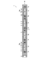
- the light source substrate unit 1 includes a plurality of LED chips 2 and a base material 10 on which the LED chips 2 (light emitting elements, light emitting chips) are mounted.
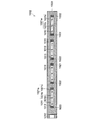
- the base material 10 includes a first resin part 11 injection-molded with a first resin, a second resin part 12 injection-molded with a second resin, and a wiring layer 13 made of metal.
- four second resin portions 12 are provided for one first resin portion 11.
- the first resin part 11, the second resin part 12, and the wiring layer 13 are integrally formed.
- the first resin portion 11, the second resin portion 12, and the wiring layer 13 are hatched in order to facilitate understanding of the structure of the base material 10.
- the surface of the second resin portion 12 on which the LED chip 2 is mounted is not hatched. The same applies to FIGS. 5 and 6 (second embodiment) and FIGS. 7 and 8 (third embodiment).
- the base material 10 is provided with a plurality of (for example, four) recesses 10a for storing the plurality of LED chips 2.
- the inner surface of the recess 10 a has a bottom surface 10 b that is a mounting surface on which the LED chip 2 is mounted, and an inner side surface 10 c that is disposed on the side of the LED chip 2.
- the number of the recessed parts 10a provided in the base material 10 can be changed suitably, and should just be two or more. Further, the number of LED chips 2 accommodated in one recess 10a can be changed as appropriate, and it is sufficient that the number is one or more.
- the inner surface (the bottom surface 10b and the inner surface 10c) of the recess 10a is formed by the second resin portion 12.
- the second resin portion 12 is provided on the main surface (light emission side surface) side of the base material 10, and is not provided on the back surface (surface opposite to the main surface) side of the base material 10.
- the LED chip 2 is bare-chip mounted on the bottom surface 10 b of the recess 10 a and is electrically connected to the adjacent LED chip 2 and the wiring layer 13 by the bonding wire 3.
- the wiring layer 13 may be extended to the center of the recess 10 a and the LED chip 2 may be mounted on the wiring layer 13.
- a part of the wiring layer 13 is exposed in the recess 10a.
- a silver layer may be provided on the surface of the wiring layer 13 in the recess 10a. Thereby, it is possible to raise the total light reflectivity of the light in the recessed part 10a.
- the configuration in which the LED chip 2 is mounted on the wiring layer 13 is particularly effective because the area of the wiring layer 13 is increased.
- the wiring layer 13 located on the leftmost side in FIGS. 1 and 2 is electrically connected to an electrode terminal (not shown) of the connector member 4. Yes.
- a wire harness (not shown) for supplying power to the LED chip 2 is connected to the connector member 4.
- a sealing resin layer 5 made of a substantially transparent resin is provided in the recess 10a, and the LED chip 2 and the bonding wire 3 are sealed by the sealing resin layer 5.
- the light source board unit 1 emits white light.
- the LED chip 2 may emit blue light
- the second resin portion 12 may contain a phosphor that converts blue light into yellow light.
- white light is obtained by mixing the blue light from the LED chip 2 and the yellow light from the second resin portion 12.
- the sealing resin layer 5 may contain a phosphor that converts light from the LED chip 2 into light of a different color. In this case, white light is obtained by mixing the light from the LED chip 2 and the light from the sealing resin layer 5.
- the light emitted from the LED chip 2 is emitted in the emission direction of the light source substrate unit 1 (upper side in FIG. 2).
- Most of the light is incident on an irradiation target (for example, a light guide plate or an illuminated member included in the module).
- an irradiation target for example, a light guide plate or an illuminated member included in the module.
- a part of the light is reflected on the surface of the irradiation target, and most of the light is irradiated on any part of the substrate 10 (mainly the inner surface of the recess 10a).
- the light applied to the base material 10 is reflected without being absorbed by the base material 10 and is applied again to the irradiation target, so that the utilization efficiency of the light emitted from the LED chip 2 is improved.
- the part (especially inner surface of the recessed part 10a) utilized for reflection has a high total light reflectance. Further, in order to suppress the change in the color tone of light due to reflection on the base material 10, it is preferable that the portion used for reflection (particularly the inner surface of the recess 10a) is white.
- the second resin portion 12 has a higher total light reflectance (one of optical characteristics) than the first resin portion 11 and is formed in a white color.
- the second resin may contain a reflectance improving filler that improves the total light reflectance. For example, if a white filler made of titanium oxide or the like is added as a reflectance improving filler to a resin such as PET (Polyethylene Terephthalate), PTFE (Polytetrafluorethylene), or LCP (Liquid Crystal Polymer), the total light reflection of the second resin portion 12 is achieved. The rate can be easily increased.
- the base material 10 needs to fix the wiring layer 13, the connector member 4 and the like, and has sufficient physical characteristics.
- the portion (first resin portion 11) other than the periphery of the recess 10 a in which optical characteristics are particularly required is formed using a resin having physical properties superior to those of the second resin portion 12.
- the first resin may contain a physical property changing filler that changes physical properties. For example, if talc powder or the like is contained in the first resin as the physical property changing filler, the rigidity of the first resin portion 11 can be easily increased.
- a polyamide resin or a polyimide resin is used as the first resin, the heat resistance of the first resin portion 11 can be improved.
- the first resin and the second resin may be made of the same material (polymer) or may be made of different materials.
- the first resin and the second resin may be made of the same material (polymer) or may be made of different materials.
- the optical characteristics and physical characteristics of both can be easily achieved. It is possible to make it different.
- Such a configuration is effective, for example, when it is desired to bring the linear expansion coefficient (one of physical properties) close to each other or to improve the adhesion between the two.
- the wiring layer 13 may be insert-molded or outsert-molded in the first resin part 11 as an insert part or an outsert part.
- the first resin part 11 and the wiring layer 13 may be insert-molded or outsert-molded in the second resin part 12 as insert parts or outsert parts. That is, the base material 10 may be formed by additionally molding the second resin by insert molding or outsert molding on the first resin portion 11 that has been injection molded.
- the 1st resin part 11 and the 2nd resin part 12 may be shape
- the base material 10 may be formed by fitting the first resin portion 11 and the second resin portion 12, and the first resin portion 11 and the second resin portion 12 are made of an adhesive (not shown).
- the base material 10 may be formed by bonding to each other using Moreover, the base material 10 may be formed by using fitting and adhesion together.
- first resin portion 11 and the second resin portion 12 may be integrally formed by multicolor molding.
- the 1st resin part 11 and the 2nd resin part 12 may be integrally formed by color mixing molding.
- the second resin after injecting the first resin, the second resin can be partially formed by pouring a reflectance improving filler.
- the light source substrate unit 1 described above can be used, for example, in an illumination device that constitutes a display device.
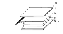
- the structure of the display device 50 including the illumination device 60 using the light source substrate unit 1 will be described.
- the display device 50 is used in, for example, a television receiver. As shown in FIGS. 3 and 4, the display device 50 includes a display panel 51 and an illumination device 60 that is disposed on the back side of the display panel 51 and illuminates the display panel 51.
- the display panel 51 is composed of a liquid crystal display panel, and has two glass substrates that sandwich a liquid crystal layer (not shown).
- the display panel 51 displays an image using light from the illumination device 60.
- the illumination device 60 is a so-called edge light type backlight device.
- the edge-light type backlight device is a device in which a light source is disposed at an edge of the backlight device and planar light is emitted using a light guide plate or the like.
- the edge-light type backlight device is advantageous in reducing the thickness of the lighting device as compared with a so-called direct-type backlight device in which a light source is disposed directly under the back surface of the illumination target member (display panel 51).
- the illuminating device 60 includes the light source substrate unit 1, a light guide plate 61 that receives light from the light source substrate unit 1 and emits light toward the display panel 51, and a rear side of the light guide plate 61 (lower side in FIG. 4).
- the light guide plate 61 is the widest surface and is provided so as to intersect the light emitting surface 61a provided on the display panel 51 side and the light emitting surface 61a, and light from which the light from the light source substrate unit 1 is incident. And an incident surface 61b. Light emitted from the light source substrate unit 1 enters the light incident surface 61 b of the light guide plate 61. The light incident on the light guide plate 61 is mixed and uniformed in the light guide plate 61 and is emitted as planar light from the light emitting surface 61a.
- the reflection sheet 62 has a function of reflecting the light leaked from the light guide plate 61 from the surface opposite to the light emitting surface 61 a (the lower surface in FIG.
- the diffusion sheet 63 has a function of uniformizing light emitted from the light emitting surface 61a of the light guide plate 61 and suppressing luminance unevenness.
- the base material 10 includes the first resin portion 11 obtained by injection molding the first resin and the second resin portion 12 obtained by injection molding the second resin.
- the 2nd resin part 12 has mutually different optical characteristics.
- a resin having good physical properties can be used as the first resin
- a resin having good optical properties can be used as the second resin.
- the base material 10 which has a favorable optical characteristic and a favorable physical characteristic can be obtained.
- the first resin is applied to a portion where the optical properties are not important. Can be used. Thereby, the usage-amount of 2nd resin can be reduced and it can suppress that the cost of the base material 10 becomes high.
- the optical characteristics of the inner surface of the recess 10a can be made different from the optical characteristics of other portions.
- the resin portion 11 and the second resin portion 12 by injection molding, for example, compared to the resin layer (resin portion) of the metal base substrate, the resin portion (the first resin portion 11 and the second resin portion).
- the degree of freedom of the shape of 12) and the degree of freedom of the material (polymer) can be improved.
- the second resin portion 12 has a higher total light reflectance than the first resin portion 11.
- the total light reflectance of the inner surface of the concave portion 10a can be increased, the light emitted from the light source substrate unit 1 and reflected by the surface of the irradiation target (for example, the light guide plate 61) is returned to the concave portion 10a. It is possible to reflect with a high total light reflectance on the inner surface of. For this reason, the utilization efficiency of light can be improved.
- the second resin portion 12 has a white color. Thereby, the color tone of the light reflected by the 2nd resin part 12 becomes difficult to change. Moreover, the total light reflectance of the 2nd resin part 12 can be made high easily.
- the LED chip 2 emits blue light
- the second resin portion 12 contains a phosphor that converts blue light into yellow light.
- the white light may be obtained by mixing the yellow light from the second resin portion 12 and the yellow light from the second resin portion 12. In this case, since the second resin portion 12 can convert blue light into yellow light, there is no need to separately provide a member containing a phosphor that converts blue light into yellow light. .
- the first resin and the second resin may be made of the same material resin, and the first resin may contain a physical property changing filler that changes physical properties.
- the physical characteristics of the first resin can be changed so that the physical characteristics of the first resin are in a desired direction.
- the first Good physical characteristics can be realized by the resin.
- the first resin and the second resin may be made of the same material resin, and the second resin may contain a reflectance improving filler that improves the total light reflectance.
- the second resin reduces the adverse effects of combining different types of resins (adhesion (adhesive strength) between the two types of resin, cracks, peeling, warping, etc. due to differences in thermal expansion coefficient and rigidity). Good total light reflectance can be realized.
- the bottom surface 10b and the inner side surface 10c of the recess 10a are formed by the second resin portion 12.
- the light emitted from the light source substrate unit 1 and reflected and returned from the surface of the irradiation target (for example, the light guide plate 61) easily reaches the bottom surface 10b and the inner side surface 10c of the recess 10a.
- the utilization efficiency of light can be further improved by forming the bottom surface 10b and the inner side surface 10c of the recess 10a with the second resin portion 12 having a high total light reflectance.
- the sealing resin layer 5 is provided in the recess 10a. Although the LED chip 2, the bonding wire 3, and their connection portions may be damaged by impact, the above-described damage can be suppressed by providing the sealing resin layer 5. Further, the sealing resin layer 5 can protect the LED chip 2 and the bonding wire 3 from moisture and foreign matter. Further, the silver layer on the surface of the wiring layer 13 can be suppressed from being oxidized. Further, as described above, the sealing resin layer 5 may contain a phosphor that converts light from the LED chip 2 into light of a different color. In this case, since the light from the LED chip 2 can be converted into light of a desired color by the phosphor by the sealing resin layer 5, a member containing a phosphor that converts the light from the LED chip 2 is separately provided. There is no need.
- the LED chip 2 is mounted on the base material 10 as a bare chip. Therefore, unlike the case where the package on which the LED chip 2 is mounted is mounted on the base material 10, the heat generated by the LED chip 2 can be directly radiated to the base material 10 without passing through the package. Thereby, it can suppress that the characteristic of LED chip 2 deteriorates or a lifetime becomes short.
- the total light reflectance of the light in the recess 10a can be further increased, so that the light utilization efficiency is further improved. be able to.
- the wiring layer 13 may be insert-molded or outsert-molded in the first resin part 11, and the first resin part 11 may be insert-molded or outsert-molded in the second resin part 12. .
- the base material 10 in which the wiring layer 13, the first resin part 11, and the second resin part 12 are in close contact with each other can be easily formed.
- first resin portion 11 and the second resin portion 12 are molded in separate steps, and the first resin portion 11 and the second resin portion 12 are combined together to form the base material 10. May be formed.
- each of the first resin portion 11 and the second resin portion 12 can be formed by an optimum method (resin material, curing temperature, etc.).
- the base material 10 may be formed by the 1st resin part 11 and the 2nd resin part 12 being fitted. In this case, the base material 10 in which the first resin portion 11 and the second resin portion 12 are integrated can be realized without using an adhesive or the like. Further, the base material 10 may be formed by bonding the first resin portion 11 and the second resin portion 12 to each other. In this case, the base material 10 in which the first resin portion 11 and the second resin portion 12 are integrated can be easily formed.
- the first resin portion 11 and the second resin portion 12 may be integrally formed by multicolor molding.
- the base material 10 in which the first resin portion 11 and the second resin portion 12 are integrated can be easily formed. Further, there is a possibility that the first resin portion 11 and the second resin portion 12 can be firmly joined.
- the base material 10 may be formed by adding a second resin to the injection-molded first resin portion 11 and performing insert molding or outsert molding.
- the base material 10 can be formed in a desired shape.
- the 2nd resin part 12 does not have sufficient hardness as an insert part or an outsert part
- the 2nd resin part 12 is formed first and the 1st resin is additionally molded after that, the 2nd resin part 12 is deformed or misaligned, and the base material 10 cannot be formed into a desired shape.
- white resin often has a low reflectance or yellowing due to heat
- the first resin portion 11 is formed after the first resin portion 11 is molded rather than the white second resin portion 12 is formed first. It is preferable to form the two resin portions 12.
- the first resin portion 11 and the second resin portion 12 may be integrally formed by color mixing molding.
- the base material 10 in which the first resin portion 11 and the second resin portion 12 are integrated can be easily formed. Further, there is a possibility that the first resin portion 11 and the second resin portion 12 can be firmly joined.
- the light source substrate unit 101 includes a plurality of LED chips 2 and a base 110 on which the LED chips 2 are mounted.
- the base material 110 includes a first resin portion 111 obtained by injection molding a first resin, a second resin portion 112 obtained by injection molding a second resin, and a wiring layer 13 made of metal.
- the first resin portion 111, the second resin portion 112, and the wiring layer 13 are hatched for easy understanding of the structure of the base material 110.
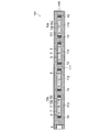
- the second resin portion 112 is formed so as to connect the plurality of second resin portions 12 of the first embodiment. Further, the first resin portion 111 is provided on the back surface side of the base material 110 and the second resin portion 112 is provided on the main surface side of the base material 110. Except for the wiring layer 13, the entire surface facing the light emitting side of the substrate 110 is formed by the second resin portion 112. Thereby, the light utilization efficiency can be further improved.
- the remaining structure of the second embodiment is the same as that of the first embodiment.
- the method of integrally forming the first resin part 111, the second resin part 112, and the wiring layer 13 is the same as in the first embodiment.
- the first resin portion 111 and the second resin portion 112 may be formed by multicolor molding or mixed color molding.
- the 1st resin part 111 and the 2nd resin part 112 are each biased in the back surface side and the main surface side of the base material 110, it becomes easy to shape
- the portion made of the second resin since the portion made of the second resin (second resin portion 112) is integrated, it is possible to inject the second resin from a common gate (mold injection port). Is possible.
- first resin part 111 and the second resin part 112 are formed in separate steps and then integrated together, the portion made of the second resin (second resin part 112) is integrated, The number of components attached to the first resin part 111 is small, and the assembly process can be simplified.
- the light source substrate unit 201 includes a plurality of LED chips 2 and a substrate 210 on which the LED chips 2 are mounted.
- the substrate 210 includes a first resin portion 211 obtained by injection molding a first resin, a second resin portion 212 obtained by injection molding a second resin, and a wiring layer 13 made of metal. 7 and 8, the first resin portion 211, the second resin portion 212, and the wiring layer 13 are hatched for easy understanding of the structure of the substrate 210.
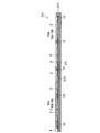
- the second resin portion 212 is provided not only on the main surface side of the substrate 210 but also on the back surface side.
- the first resin portion 211 is covered with the second resin portion 212 and is not exposed to the outside.
- the substrate 210 is integrally formed by sandwich molding (a kind of color mixing molding) in which the first resin is a core resin and the second resin is a skin resin.
- the 2nd resin part 212 may be isolate
- the substrate 210 can be formed by the same method as in the first embodiment or the second embodiment.
- the main surface side and the back surface side of the base material 10 are formed by the second resin portion 12.
- the first resin portion 11 and the second resin portion 12 may be integrally formed by sandwich molding using the first resin as the core resin and the second resin as the skin resin. In this case, a portion (a main surface side of the base material 10) that requires good optical characteristics can be easily formed by the second resin portion 12.
- substrate unit was shown about the example used for the backlight apparatus which illuminates a display panel, this invention is not restricted to this,
- the illumination apparatus which illuminates to-be-illuminated members other than a display panel Is also applicable.
- the present invention can also be applied to a ceiling illumination device provided with a panel (illuminated member), an illumination device that illuminates a sign board (illuminated member) from the back side, and the like.
- a light emitting element including a package on which a light emitting chip is mounted may be mounted on a base material.
- an LED chip is used as the light emitting chip.
- the present invention is not limited to this, and a light emitting chip other than the LED chip may be used.
- white light is obtained using an LED chip that emits blue light and a phosphor that converts blue light into yellow light
- white light may be obtained using three types of light emitting chips that respectively emit red light, green light, and blue light.
- white light may be obtained using an LED chip that emits ultraviolet light and three types of phosphors that convert ultraviolet light into, for example, red light, green light, and blue light.
- the light source substrate unit is configured to emit white light.
- the present invention is not limited thereto, and the light source substrate unit is configured to emit light other than white light. May be.
- the main surface side of the base material is formed by the second resin portion and the back surface side of the base material is formed by the first resin portion.
- the present invention is not limited thereto. Absent. You may form the main surface side of a base material with the 1st resin part and the 2nd resin part. Similarly, you may form the back surface side of a base material with the 1st resin part and the 2nd resin part. The amount (area and thickness) of the second resin portion on the main surface side of the base material and the amount (area and thickness) of the second resin portion on the back surface side of the base material are appropriate so that the warpage of the base material becomes smaller Should be set.
- the material (polymer) of 1st resin and 2nd resin when the material (polymer) of 1st resin and 2nd resin was the same, it showed about the example which makes the presence or absence, kind, and content of a filler differ, but this invention is this. Not limited to.
- the material of the first resin and the second resin may be the same, and the presence / absence / type / content of the filler may be the same.
- the first resin portion and the second resin portion after molding can be changed by changing the curing conditions for the first resin and the second resin, or by adding or changing pretreatment / posttreatment. It is only necessary to have different characteristics (optical characteristics and physical characteristics).
- the present invention is not limited thereto. Since the required optical characteristics differ depending on the usage pattern of the light source substrate unit, the optical characteristics other than the total light reflectance of the second resin portion are different from the optical characteristics other than the total light reflectance of the first resin portion. Also good.
- a resin having a high reflectance with respect to light having a specific wavelength for example, light emitted from the light source substrate unit
- the light utilization efficiency can be improved.
- a resin having a wide diffused light distribution characteristic may be used for the second resin portion. In this case, the light reflected and returned from the irradiation target can be efficiently diffused and reflected.
- Light source substrate unit 2 LED chip (light emitting element, light emitting chip) 5 Sealing resin layer 10, 110, 210 Base material 10a Recessed part 10b Bottom face 10c Inner side face 11, 111, 211 First resin part 12, 112, 212 Second resin part 13 Wiring layer
Landscapes
- Physics & Mathematics (AREA)
- General Physics & Mathematics (AREA)
- Optics & Photonics (AREA)
- Engineering & Computer Science (AREA)
- General Engineering & Computer Science (AREA)
- Planar Illumination Modules (AREA)
- Led Device Packages (AREA)
- Arrangement Of Elements, Cooling, Sealing, Or The Like Of Lighting Devices (AREA)
- Fastening Of Light Sources Or Lamp Holders (AREA)
Abstract
樹脂部の形状および材質の自由度を向上させるとともに、コストが高くなるのを抑制し、かつ、光学的特性および物理的特性の両立を図ることが可能な照明装置を提供する。この光源基板ユニット(1)は、複数のLEDチップ(2)と、LEDチップが実装される複数の凹部(10a)を有する基材(10)とを備える。基材は第1の樹脂を射出成型した第1樹脂部(11)と第2の樹脂を射出成型した第2樹脂部(12)とを含み、第1樹脂部および第2樹脂部は互いに異なる光学的特性を有し、凹部の内面の少なくとも一部は、第2樹脂部により形成されている。
Description
この発明は、光源基板ユニットに関し、特に、複数の発光素子と複数の発光素子が実装される基材とを備えた光源基板ユニットに関する。
近年、光源としての発光ダイオード(LED:Light Emitting Diode)を備えた光源基板ユニットや、この光源基板ユニットを用いた光源モジュールの用途が広がっている。従来、液晶表示装置用のバックライト装置の光源としては、冷陰極管(CCFL:Cold Cathode Fluorescent Lamp)が主流であったが、LED素子(発光素子)への置き換えが急速に進んでいる。この置き換えにより、環境負荷の高い水銀の使用を廃止し、消費電力を削減し、かつ、バックライト装置の長寿命化を図ることが可能になる。
このような光源基板ユニットとしては、COB(Chip On Board)実装と呼ばれる方法でLEDチップからなるLED素子(発光素子)を基板に直接実装したものや、LEDチップが搭載されたLEDパッケージからなるLED素子を基板に実装したものが知られている。
なお、本明細書および請求の範囲において、発光素子とは、発光チップ(LEDチップなど)そのものと、発光チップが搭載されたパッケージ(LEDパッケージなど)との両方を含む概念である。
図9および図10は、LEDチップからなるLED素子を基板に直接実装した光源基板ユニットを備えた従来のバックライト装置の構造の一例を概略的に示した図である。図11および図12は、図9に示した従来のバックライト装置の光源基板ユニットの構造を示した図である。バックライト装置1001は液晶表示パネル(図示せず)に対して光を照射するものである。バックライト装置1001は図9に示すように、光源基板ユニット1002と、光源基板ユニット1002からの光が入射され、液晶表示パネル側(図9の上側)に光を出射する導光板1003と、導光板1003の背面側(図9の下側)に配置される反射シート1004と、導光板1003上に配置される拡散シート1005と、光源基板ユニット1002および導光板1003などを収納する筐体1006とを備えている。
導光板1003は、最も広い面であるとともに液晶表示パネル側(図9では上側)に設けられた光出射面1003aと、光出射面1003aに対して交差して設けられるとともに光源基板ユニット1002からの光が入射される光入射面1003b(図10参照)とを有する。光源基板ユニット1002から出射した光は、導光板1003の光入射面1003bに入射する。導光板1003に入射した光は、導光板1003内で混ざり合い均一化されて、光出射面1003aから面状光として出射する。反射シート1004は導光板1003から光出射面1003aとは反対側の面(図9では下面)から漏れた光を反射して導光板1003内に戻す機能を有する。これにより、光の利用効率を向上させることができる。拡散シート1005は導光板1003の光出射面1003aから出射した光を均一化し、輝度ムラを抑制する機能を有する。
光源基板ユニット1002は図11および図12に示すように、複数のLEDチップ1010と、LEDチップ1010が実装される基材1020とを含んでいる。基材1020は略平板状の樹脂部1021と、樹脂部1021と一体で形成された配線層1022とを含んでいる。樹脂部1021にはLEDチップ1010を収納する凹部1021aが複数設けられている。凹部1021aの内面はLEDチップ1010が実装される実装面である底面1021bと、LEDチップ1010の周囲を囲う内側面1021cとを有する。樹脂部1021は樹脂を射出成型することにより形成されている。なお、図11および図12では、基材1020の構造を理解しやすくするために、樹脂部1021および配線層1022にハッチングを施している。ただし、樹脂部1021のうちのLEDチップ1010が実装される面には、ハッチングを施していない。
LEDチップ1010は凹部1021aの底面1021bに実装されているとともに、ボンディングワイヤ1011により隣接するLEDチップ1010や配線層1022に電気的に接続されている。基材1020に設けられた複数の配線層1022の中で、図11および図12において最も左側に位置する配線層1022は、コネクタ部材1012の電極端子(図示せず)に電気的に接続されている。このコネクタ部材1012には、LEDチップ1010に電力を供給するためのワイヤハーネス(図示せず)が接続されている。
また、凹部1021a内には、LEDチップ1010およびボンディングワイヤ1011を封止する封止樹脂1013が設けられている。
このバックライト装置1001では、基材1020の樹脂部1021は射出成型により形成されるので、樹脂部1021の形状の自由度および樹脂部1021の材質の自由度を向上させることが可能である。
なお、LEDチップからなるLED素子(発光素子)を基板に直接実装した照明装置は、例えば特許文献1に開示されている。この特許文献1では、装置基板(基板)は金属ベースド基板(金属ベース基板とも言う)からなる。金属ベース基板とは、金属板をベース基材としてその表面上に樹脂層や配線層を積層したものである。
ところで、光源基板ユニット1002の樹脂部1021に用いられる樹脂は、良好な光学的特性と良好な物理的特性とを兼ね備えている必要がある。例えば、樹脂部1021に用いられる樹脂は、光の反射率(光学的特性の1つ)が高いことが好ましい。このように構成すれば、光源基板ユニット1002から出射した光の一部が導光板1003の光入射面1003bで反射された場合に、その反射光を樹脂部1021により導光板1003側に反射して導光板1003に入射させることができる。これにより、光の利用効率を向上させることができる。また、樹脂部1021での反射の際に光の色調が変化するのを抑制するために、樹脂部1021の色調(光学的特性の1つ)も重要である。また、樹脂部1021に用いられる樹脂は、例えば剛性、弾性、耐衝撃性、耐摩耗性、耐熱性および線膨張係数などの物理的特性が良好なものが選定される。
しかしながら、良好な光学的特性と良好な物理的特性との両方を高い水準で満たすのは、一般的に困難である。あるいは、たとえ光学的特性と物理的特性とを高い水準で満たす樹脂があったとしても、使用できる原材料が限定されると、コストが高くなる可能性がある。
なお、本明細書および請求の範囲において、光学的特性とは、全光線反射率、鏡面反射率、拡散反射率、反射率の波長分布、色調、拡散反射の配光特性、光の入射角と拡散反射の配光特性との関係などを含む概念である。また、物理的特性とは、剛性、弾性、耐衝撃性、耐摩耗性、耐熱性および線膨張係数などを含む概念である。
また、特許文献1のように、金属板をベース基材としてその表面上に樹脂層や配線層を積層したものを用いる場合、樹脂層(樹脂部)の形状の自由度や樹脂の材質(ポリマー)の自由度を向上させるのは困難であるという問題点がある。
この発明は、上記のような課題を解決するためになされたものであり、この発明の目的は、樹脂部の形状および材質の自由度を向上させるとともに、コストが高くなるのを抑制し、かつ、光学的特性および物理的特性の両立を図ることが可能な光源基板ユニットを提供することである。
上記目的を達成するために、この発明の光源基板ユニットは、複数の発光素子と、発光素子が実装される複数の凹部を有する基材とを備え、基材は第1の樹脂を射出成型した第1樹脂部と第2の樹脂を射出成型した第2樹脂部とを含み、第1樹脂部および第2樹脂部は互いに異なる光学的特性を有し、凹部の内面の少なくとも一部は、第2樹脂部により形成されている。
この光源基板ユニットでは、上記のように、基材は第1の樹脂を射出成型した第1樹脂部と第2の樹脂を射出成型した第2樹脂部とを含み、第1樹脂部および第2樹脂部は互いに異なる光学的特性を有する。これにより、例えば、第1の樹脂としては良好な物理的特性を有する樹脂を使用し、第2の樹脂としては良好な光学的特性を有する樹脂を使用することができる。このため、良好な光学的特性と良好な物理的特性とを兼ね備えた基材を得ることができる。あるいは、仮に第2の樹脂が良好な光学的特性と良好な物理的特性とを有していたとしても、第2の樹脂が高価な場合、光学的特性が重要でない部分に第1の樹脂を使用することができる。これにより、第2の樹脂の使用量を削減して、基材のコストが高くなるのを抑制することができる。
また、凹部の内面の少なくとも一部を第2樹脂部により形成することによって、凹部の内面の少なくとも一部の光学的特性を、他の部分の光学的特性と異ならせることができる。
また、射出成型により第1樹脂部および第2樹脂部を形成することによって、例えば金属ベース基板の樹脂層(樹脂部)に比べて、樹脂部(第1樹脂部および第2樹脂部)の形状の自由度および材質(ポリマー)の自由度を向上させることができる。
上記光源基板ユニットにおいて、好ましくは、第2樹脂部は第1樹脂部よりも高い全光線反射率を有する。このように構成すれば、凹部の内面の少なくとも一部の全光線反射率を高くすることができる。これにより、光源基板ユニットから出射して反射などにより戻ってきた光を、凹部の内面の少なくとも一部により高い全光線反射率で反射させることができる。このため、光の利用効率を向上させることができる。
なお、全光線反射率とは、鏡面反射率と拡散反射率との和である。
上記光源基板ユニットにおいて、好ましくは、第2樹脂部は白色系の色である。このように構成すれば、第2樹脂部で反射される光の色調が変化しにくくなる。
上記光源基板ユニットにおいて、好ましくは、発光素子は青色系の光を発光し、第2樹脂部は青色系の光を黄色系の光に変換する蛍光体を含有し、発光素子からの青色系の光および第2樹脂部からの黄色系の光が混色されることにより白色系の光が得られる。このように構成すれば、第2樹脂部により青色系の光を黄色系の光に変換することができるので、青色系の光を黄色系の光に変換する蛍光体を含有する部材を別途設ける必要がない。
上記光源基板ユニットにおいて、好ましくは、第1の樹脂および第2の樹脂は、同一の材質の樹脂により構成され、第1の樹脂は物理的特性を変える物理的特性変更フィラーを含有する。このように構成すれば、第1の樹脂の物理的特性が望ましい方向に向かうように第1の樹脂の物理的特性を変えることができる。これにより、異なる材質(ポリマー)の樹脂を組み合わせることによる弊害(2種類の樹脂の密着性(接着強度)、熱膨張係数や剛性の相違による亀裂・剥離・反りなど)を抑制しながら、第1の樹脂により良好な物理的特性を実現することができる。
上記光源基板ユニットにおいて、好ましくは、第1の樹脂および第2の樹脂は、同一の材質の樹脂により構成され、第2の樹脂は全光線反射率を向上させる反射率向上フィラーを含有する。このように構成すれば、異なる材質の樹脂を組み合わせることによる弊害(2種類の樹脂の密着性(接着強度)、熱膨張係数や剛性の相違による亀裂・剥離・反りなど)を抑制しながら、第2の樹脂により良好な全光線反射率を実現することができる。
上記光源基板ユニットにおいて、好ましくは、第1の樹脂および第2の樹脂は、互いに異なる材質の樹脂により構成され、基材の主表面の少なくとも一部および裏面の少なくとも一部は、第2樹脂部により形成されている。このように構成すれば、第1樹脂部の熱膨張係数と第2樹脂部の熱膨張係数とが異なる場合であっても、基材に生じる反りを抑制することができる。
上記光源基板ユニットにおいて、好ましくは、凹部は発光素子が実装される底面と、発光素子の側方に配置される内側面とを有し、底面と内側面との少なくとも一部は、第2樹脂部により形成されている。このように構成すれば、凹部の内面のうち、光学的特性が特に重要である底面と内側面との少なくとも一部の光学的特性を、他の部分の光学的特性と異ならせることができる。
上記光源基板ユニットにおいて、好ましくは、凹部内に封止樹脂層が設けられており、封止樹脂層は発光素子からの光を異なる色の光に変換する蛍光体を含有する。このように構成すれば、発光素子からの光を蛍光体により所望の色の光に変換しながら、発光素子を封止樹脂層により保護することができる。
上記光源基板ユニットにおいて、好ましくは、発光素子は発光チップからなり、基材には配線層が設けられており、発光チップは凹部の底面または配線層にベアチップ実装されているとともに、配線層に電気的に接続されている。このように構成すれば、発光チップが搭載されたパッケージを基材に実装する場合と異なり、発光チップで発生した熱をパッケージを介さず直接的に基材に放熱することができる。これにより、発光素子の特性が劣化したり寿命が短くなるのを抑制することができる。
この場合、好ましくは、配線層は凹部内に露出しており、凹部内の配線層の少なくとも一部の表面には、銀層が設けられている。このように構成すれば、光源基板ユニットから出射して反射などにより戻ってきた光を、銀層により反射させることができるので、光の利用効率を向上させることができる。
上記基材に配線層が設けられている光源基板ユニットにおいて、好ましくは、配線層は第1樹脂部にインサート成型またはアウトサート成型されており、第1樹脂部は第2樹脂部にインサート成型またはアウトサート成型されている。このように構成すれば、配線層、第1樹脂部および第2樹脂部が互いに密着した基材を容易に形成することができる。
なお、インサート成型とは、金型にインサート部品(金属部品や樹脂成型品など)をセットし、樹脂を流し込むことで、インサート部品と樹脂部とを一体に形成することを言う。アウトサート成型とは、金型にアウトサート部品(金属部品や樹脂成型品など)をセットし、樹脂を流し込むことで、アウトサート部品と樹脂部とを一体に形成することを言う。アウトサート成型は、金属部品や樹脂成型品などの一部に(局所的に)樹脂部を形成する点で、インサート成型と異なる。
上記光源基板ユニットにおいて、好ましくは、第1樹脂部および第2樹脂部は別々の工程で成型されており、第1樹脂部および第2樹脂部が一体に組み合わされることにより、基材が形成されている。このように構成すれば、第1樹脂部および第2樹脂部を、それぞれ最適な方法(樹脂の材質や硬化温度など)で形成することができる。
上記第1樹脂部および第2樹脂部が別々の工程で成型されている光源基板ユニットにおいて、好ましくは、第1樹脂部および第2樹脂部が嵌合されることにより、基材が形成されている。このように構成すれば、接着材等を用いることなく、第1樹脂部と第2樹脂部とが一体化された基材を実現することができる。
上記第1樹脂部および第2樹脂部が別々の工程で成型されている光源基板ユニットにおいて、好ましくは、第1樹脂部および第2樹脂部が互いに接着されることにより、基材が形成されている。このように構成すれば、第1樹脂部と第2樹脂部とが一体化された基材を容易に形成することができる。
上記光源基板ユニットにおいて、好ましくは、第1樹脂部および第2樹脂部は多色成型により一体に形成されている。このように構成すれば、第1樹脂部と第2樹脂部とが一体化された基材を容易に形成することができる。また、第1樹脂部と第2樹脂部とを強固に接合できる可能性がある。
なお、多色成型とは、色、材質または硬度などが異なる2種類以上の樹脂を使用した成型方法であり、先に成型した一次成型物の全部または一部に、異なる樹脂からなる二次成型物を一体に成型することを言う。
上記光源基板ユニットにおいて、好ましくは、第1樹脂部および第2樹脂部がインサート成型またはアウトサート成型により一体に組み合わされることによって、基材が形成されている。このように構成すれば、第1樹脂部および第2樹脂部が互いに密着した基材を容易に形成することができる。
この場合、好ましくは、射出成型された第1樹脂部に第2の樹脂が追加されてインサート成型またはアウトサート成型されることによって、基材が形成されている。このように構成すれば、例えば第2樹脂部がインサート部品またはアウトサート部品としては十分な硬さがなかったとしても、基材を所望の形状に形成することができる。なお、第2樹脂部がインサート部品またはアウトサート部品としては十分な硬さがない場合に、第2樹脂部を先に形成し、その後第1の樹脂を追加成型すると、第2樹脂部に変形やズレが生じて、基材を所望の形状に形成することができない。
上記光源基板ユニットにおいて、好ましくは、第1樹脂部および第2樹脂部は混色成型により一体に形成されている。このように構成すれば、第1樹脂部と第2樹脂部とが一体化された基材を容易に形成することができる。また、第1樹脂部と第2樹脂部とを強固に接合できる可能性がある。
なお、混色成型とは、色、材質または硬度などが異なる2種類以上の樹脂を使用した成型方法であり、複数の樹脂を例えば順にまたは交互に射出して、一体に成型することを言う。
この場合、好ましくは、第1樹脂部および第2樹脂部は、第1の樹脂をコア樹脂とし第2の樹脂をスキン樹脂としたサンドイッチ成型により一体に形成されている。このように構成すれば、良好な光学的特性が必要な部分(例えば基材の主表面)を、第2樹脂部により容易に形成することができる。
なお、サンドイッチ成型とは、混色成型の一種であり、スキン層(外層)を形成するスキン樹脂を金型に注入(射出)し、このスキン樹脂の内部にコア層(内層)を形成するコア樹脂を注入(射出)して、これらの樹脂を硬化させることによって、多層構造の成型物を得る方法を言う。
以上のように、本発明によれば、樹脂部の形状および材質の自由度を向上させるとともに、コストが高くなるのを抑制し、かつ、光学的特性および物理的特性の両立を図ることが可能な光源基板ユニットを容易に得ることができる。
以下、本発明の実施形態について図面を参照して説明する。なお、理解を容易にするために、断面図であってもハッチングを施さない場合や、断面図でなくてもハッチングを施す場合がある。
(第1実施形態)
図1~図4を参照して、本発明の第1実施形態による光源基板ユニット1の構造について説明する。光源基板ユニット1は図1および図2に示すように、複数のLEDチップ2と、LEDチップ2(発光素子、発光チップ)が実装される基材10とを含んでいる。基材10は、第1の樹脂を射出成型した第1樹脂部11と、第2の樹脂を射出成型した第2樹脂部12と、金属からなる配線層13とを含んでいる。本実施形態では、1個の第1樹脂部11に対して4個の第2樹脂部12が設けられている。第1樹脂部11、第2樹脂部12および配線層13は一体に形成されている。なお、図1および図2では、基材10の構造を理解しやすくするために、第1樹脂部11、第2樹脂部12および配線層13にハッチングを施している。ただし、第2樹脂部12のうちのLEDチップ2が実装される面には、ハッチングを施していない。このことは、図5および図6(第2実施形態)、図7および図8(第3実施形態)も同様である。
図1~図4を参照して、本発明の第1実施形態による光源基板ユニット1の構造について説明する。光源基板ユニット1は図1および図2に示すように、複数のLEDチップ2と、LEDチップ2(発光素子、発光チップ)が実装される基材10とを含んでいる。基材10は、第1の樹脂を射出成型した第1樹脂部11と、第2の樹脂を射出成型した第2樹脂部12と、金属からなる配線層13とを含んでいる。本実施形態では、1個の第1樹脂部11に対して4個の第2樹脂部12が設けられている。第1樹脂部11、第2樹脂部12および配線層13は一体に形成されている。なお、図1および図2では、基材10の構造を理解しやすくするために、第1樹脂部11、第2樹脂部12および配線層13にハッチングを施している。ただし、第2樹脂部12のうちのLEDチップ2が実装される面には、ハッチングを施していない。このことは、図5および図6(第2実施形態)、図7および図8(第3実施形態)も同様である。
また、基材10には、複数のLEDチップ2を収納する凹部10aが複数(例えば4個)設けられている。凹部10aの内面はLEDチップ2が実装される実装面である底面10bと、LEDチップ2の側方に配置される内側面10cとを有する。なお、基材10に設けられる凹部10aの数は適宜変更可能であり、2個以上あればよい。また、1つの凹部10aに収納されるLEDチップ2の数は適宜変更可能であり、1個以上あればよい。
本実施形態では、凹部10aの内面(底面10bおよび内側面10c)は、第2樹脂部12により形成されている。第2樹脂部12は基材10の主表面(光出射側の面)側に設けられており、基材10の裏面(主表面とは反対側の面)側には設けられていない。
LEDチップ2は凹部10aの底面10bにベアチップ実装されており、ボンディングワイヤ3により隣接するLEDチップ2や配線層13に電気的に接続されている。なお、配線層13を凹部10aの中央まで延設し、LEDチップ2を配線層13に実装してもよい。配線層13の一部は凹部10a内に露出している。凹部10a内の配線層13の表面には、銀層が設けられていてもよい。これにより、凹部10aにおける光の全光線反射率を高くすることが可能である。LEDチップ2を配線層13上に実装する構成では配線層13の面積が大きくなるので、特に有効である。基材10に設けられた複数の配線層13の中で、図1および図2において最も左側に位置する配線層13は、コネクタ部材4の電極端子(図示せず)に電気的に接続されている。このコネクタ部材4には、LEDチップ2に電力を供給するためのワイヤハーネス(図示せず)が接続されている。
また、凹部10a内には、略透明な樹脂からなる封止樹脂層5が設けられており、LEDチップ2およびボンディングワイヤ3は、封止樹脂層5により封止されている。
光源基板ユニット1は白色光を出射する。例えば、LEDチップ2が青色光を発光し、第2樹脂部12が青色光を黄色光に変換する蛍光体を含有していてもよい。この場合、LEDチップ2からの青色光および第2樹脂部12からの黄色光が混色されることにより、白色光が得られる。また例えば、封止樹脂層5がLEDチップ2からの光を異なる色の光に変換する蛍光体を含有していてもよい。この場合、LEDチップ2からの光および封止樹脂層5からの光が混色されることにより、白色光が得られる。
ここで、LEDチップ2から出射した光は、光源基板ユニット1の出射方向(図2の上側)に出射する。そして、大部分の光は照射対象(例えばモジュールに含まれる導光板や被照明部材等)に入射する。このとき、一部の光は照射対象の表面で反射され、そのうちの大部分が基材10のいずれかの部分(主に凹部10aの内面)に照射される。この基材10に照射される光が基材10で吸収されずに反射され照射対象に再度照射されることによって、LEDチップ2から出射する光の利用効率が向上することになる。このため、反射に利用される部分(特に凹部10aの内面)は全光線反射率が高いことが好ましい。また、基材10での反射によって光の色調が変化するのを抑制するために、反射に利用される部分(特に凹部10aの内面)は白色であることが好ましい。
したがって、第2樹脂部12は第1樹脂部11よりも高い全光線反射率(光学的特性の1つ)を有するとともに、白色系の色に形成されている。第2の樹脂には全光線反射率を向上させる反射率向上フィラーが含有されていてもよい。例えば、反射率向上フィラーとして酸化チタン等からなる白色フィラーをPET(Polyethylene Terephthalate)、PTFE(Polytetrafluoroethylene)、LCP(Liquid Crystal Polymer)等の樹脂に含有させれば、第2樹脂部12の全光線反射率を容易に高くすることが可能である。
また、基材10は配線層13やコネクタ部材4等を固定する必要があり、十分な物理的特性を有する必要がある。このため、光学的特性が特に要求される凹部10a周辺以外の部分(第1樹脂部11)は、第2樹脂部12よりも物理的特性が優れた樹脂を用いて形成されている。第1の樹脂には物理的特性を変える物理的特性変更フィラーが含有されていてもよい。例えば、物理的特性変更フィラーとしてタルク粉末等を第1の樹脂に含有させれば、第1樹脂部11の剛性を容易に高くすることが可能である。また、第1の樹脂として例えばポリアミド樹脂やポリイミド樹脂等を用いれば、第1樹脂部11の耐熱性を向上させることが可能である。
上記のように、第1の樹脂および第2の樹脂は、同一の材質(ポリマー)の樹脂により構成されていてもよいし、互いに異なる材質の樹脂により構成されていてもよい。例えば、第1の樹脂および第2の樹脂として同一の材質(ポリマー)の樹脂を用いても、フィラーの有無・種類・含有量を異ならせれば、両者の光学的特性および物理的特性を容易に異ならせることが可能である。このような構成は、両者の間で例えば線膨張係数(物理的特性の1つ)を近づけたい場合や、両者の間の密着性を向上させたい場合に有効である。
第1樹脂部11、第2樹脂部12および配線層13を一体に形成する方法は様々なものがある。
例えば、配線層13はインサート部品またはアウトサート部品として、第1樹脂部11にインサート成型またはアウトサート成型されていてもよい。そして、第1樹脂部11および配線層13はインサート部品またはアウトサート部品として、第2樹脂部12にインサート成型またはアウトサート成型されていてもよい。すなわち、射出成型された第1樹脂部11にインサート成型またはアウトサート成型により第2の樹脂が追加成型されることにより、基材10が形成されていてもよい。
また、第1樹脂部11および第2樹脂部12は別々の工程で成型されていてもよい。この場合、第1樹脂部11および第2樹脂部12が嵌合されることにより基材10が形成されていてもよいし、第1樹脂部11および第2樹脂部12が接着材(図示せず)を用いて互いに接着されることにより、基材10が形成されていてもよい。また、嵌合と接着とを併用して、基材10が形成されていてもよい。
また、第1樹脂部11および第2樹脂部12は、多色成型により一体に形成されていてもよい。また、第1樹脂部11および第2樹脂部12は、混色成型により一体に形成されていてもよい。この場合、例えば、第1の樹脂を射出した後、反射率向上フィラーを流し込むことによって、部分的に第2の樹脂とすることも可能である。
上記した光源基板ユニット1は、例えば表示装置を構成する照明装置に用いることができる。以下、光源基板ユニット1を用いた照明装置60を備えた表示装置50の構造について説明する。
表示装置50は例えばテレビジョン受像機などに用いられるものである。表示装置50は図3および図4に示すように、表示パネル51と、表示パネル51の背面側に配置され、表示パネル51を照明する照明装置60とを備えている。
表示パネル51は液晶表示パネルからなり、図示しない液晶層を挟み込む2枚のガラス基板を有する。また、表示パネル51は照明装置60からの光を利用して画像を表示する。
照明装置60は所謂エッジライト型のバックライト装置である。エッジライト型のバックライト装置とは、バックライト装置の縁部に光源を配置し、導光板等を用いて面状光を出射するものを言う。エッジライト型のバックライト装置では、被照明部材(表示パネル51)の背面直下に光源を配置する所謂直下型のバックライト装置に比べて、照明装置の薄型化に有利である。
照明装置60は、上記光源基板ユニット1と、光源基板ユニット1からの光が入射され、表示パネル51側に光を出射する導光板61と、導光板61の背面側(図4の下側)に配置される反射シート62と、導光板61上に配置される拡散シート63と、光源基板ユニット1および導光板61などを収納する筐体64とを備えている。
導光板61は、最も広い面であるとともに表示パネル51側に設けられた光出射面61aと、光出射面61aに対して交差して設けられるとともに光源基板ユニット1からの光が入射される光入射面61bとを有する。光源基板ユニット1から出射した光は、導光板61の光入射面61bに入射する。導光板61に入射した光は、導光板61内で混ざり合い均一化されて、光出射面61aから面状光として出射する。反射シート62は導光板61から光出射面61aとは反対側の面(図4の下面)から漏れた光を反射して導光板61内に戻す機能を有する。これにより、光の利用効率を向上させることができる。拡散シート63は導光板61の光出射面61aから出射した光を均一化し、輝度ムラを抑制する機能を有する。
本実施形態では、上記のように、基材10は第1の樹脂を射出成型した第1樹脂部11と第2の樹脂を射出成型した第2樹脂部12とを含み、第1樹脂部11および第2樹脂部12は互いに異なる光学的特性を有する。これにより、例えば、第1の樹脂としては良好な物理的特性を有する樹脂を使用し、第2の樹脂としては良好な光学的特性を有する樹脂を使用することができる。このため、良好な光学的特性と良好な物理的特性とを兼ね備えた基材10を得ることができる。あるいは、仮に第2の樹脂が良好な光学的特性と良好な物理的特性とを有していたとしても、第2の樹脂が高価な場合、光学的特性が重要でない部分に第1の樹脂を使用することができる。これにより、第2の樹脂の使用量を削減して、基材10のコストが高くなるのを抑制することができる。
また、上記のように、凹部10aの内面を第2樹脂部12により形成することによって、凹部10aの内面の光学的特性を他の部分の光学的特性と異ならせることができる。
また、射出成型により第1樹脂部11および第2樹脂部12を形成することによって、例えば金属ベース基板の樹脂層(樹脂部)に比べて、樹脂部(第1樹脂部11および第2樹脂部12)の形状の自由度および材質(ポリマー)の自由度を向上させることができる。
また、上記のように、第2樹脂部12は第1樹脂部11よりも高い全光線反射率を有する。これにより、凹部10aの内面の全光線反射率を高くすることができるので、光源基板ユニット1から出射して照射対象(例えば導光板61)の表面で反射されて戻ってきた光を、凹部10aの内面により高い全光線反射率で反射させることができる。このため、光の利用効率を向上させることができる。
また、上記のように、第2樹脂部12は白色系の色である。これにより、第2樹脂部12で反射される光の色調が変化しにくくなる。また、第2樹脂部12の全光線反射率を容易に高くすることができる。
また、上記のように、LEDチップ2は青色系の光を発光し、第2樹脂部12は青色系の光を黄色系の光に変換する蛍光体を含有し、LEDチップ2からの青色系の光および第2樹脂部12からの黄色系の光が混色されることにより白色光を得てもよい。この場合、第2樹脂部12により青色系の光を黄色系の光に変換することができるので、青色系の光を黄色系の光に変換する蛍光体を含有する部材を別途設ける必要がない。
また、上記のように、第1の樹脂および第2の樹脂は、同一の材質の樹脂により構成され、第1の樹脂は物理的特性を変える物理的特性変更フィラーを含有してもよい。この場合、第1の樹脂の物理的特性が望ましい方向に向かうように第1の樹脂の物理的特性を変えることができる。これにより、異なる材質(ポリマー)の樹脂を組み合わせることによる弊害(2種類の樹脂の密着性(接着強度)、熱膨張係数や剛性の相違による亀裂・剥離・反りなど)を抑制しながら、第1の樹脂により良好な物理的特性を実現することができる。
また、上記のように、第1の樹脂および第2の樹脂は、同一の材質の樹脂により構成され、第2の樹脂は全光線反射率を向上させる反射率向上フィラーを含有してもよい。この場合、異なる材質の樹脂を組み合わせることによる弊害(2種類の樹脂の密着性(接着強度)、熱膨張係数や剛性の相違による亀裂・剥離・反りなど)を抑制しながら、第2の樹脂により良好な全光線反射率を実現することができる。
また、上記のように、凹部10aの底面10bおよび内側面10cは、第2樹脂部12により形成されている。光源基板ユニット1から出射して照射対象(例えば導光板61)の表面で反射されて戻ってきた光は、凹部10aの底面10bおよび内側面10cに到達しやすい。このため、凹部10aの底面10bおよび内側面10cを全光線反射率の高い第2樹脂部12により形成することによって、光の利用効率をより向上させることができる。
また、上記のように、凹部10a内に封止樹脂層5を設けている。LEDチップ2、ボンディングワイヤ3およびこれらの接続部分は衝撃により破損することがあるが、封止樹脂層5を設けることによって、上記破損を抑制することができる。また、封止樹脂層5により、LEDチップ2やボンディングワイヤ3を水分や異物から保護することができる。また、配線層13の表面の銀層が酸化するのを抑制することができる。さらに、上記のように、封止樹脂層5はLEDチップ2からの光を異なる色の光に変換する蛍光体を含有してもよい。この場合、封止樹脂層5によりLEDチップ2からの光を蛍光体により所望の色の光に変換することができるので、LEDチップ2からの光を変換する蛍光体を含有する部材を別途設ける必要がない。
また、上記のように、LEDチップ2は基材10にベアチップ実装されている。これにより、LEDチップ2が搭載されたパッケージを基材10に実装する場合と異なり、LEDチップ2で発生した熱をパッケージを介さず直接的に基材10に放熱することができる。これにより、LEDチップ2の特性が劣化したり寿命が短くなるのを抑制することができる。
また、上記のように、凹部10a内の配線層13の表面に銀層を設ければ、凹部10aにおける光の全光線反射率をより高くすることができるので、光の利用効率をより向上させることができる。
また、上記のように、配線層13は第1樹脂部11にインサート成型またはアウトサート成型されており、第1樹脂部11は第2樹脂部12にインサート成型またはアウトサート成型されていてもよい。この場合、配線層13、第1樹脂部11および第2樹脂部12が互いに密着した基材10を容易に形成することができる。
また、上記のように、第1樹脂部11および第2樹脂部12は別々の工程で成型されており、第1樹脂部11および第2樹脂部12が一体に組み合わされることにより、基材10が形成されていてもよい。この場合、第1樹脂部11および第2樹脂部12を、それぞれ最適な方法(樹脂の材質や硬化温度など)で形成することができる。
そして、第1樹脂部11および第2樹脂部12が嵌合されることにより、基材10が形成されていてもよい。この場合、接着材等を用いることなく、第1樹脂部11と第2樹脂部12とが一体化された基材10を実現することができる。また、第1樹脂部11および第2樹脂部12が互いに接着されることにより、基材10が形成されていてもよい。この場合、第1樹脂部11と第2樹脂部12とが一体化された基材10を容易に形成することができる。
また、上記のように、第1樹脂部11および第2樹脂部12は多色成型により一体に形成されていてもよい。この場合、第1樹脂部11と第2樹脂部12とが一体化された基材10を容易に形成することができる。また、第1樹脂部11と第2樹脂部12とを強固に接合できる可能性がある。
また、上記のように、射出成型された第1樹脂部11に第2の樹脂が追加されてインサート成型またはアウトサート成型されることによって、基材10が形成されていてもよい。この場合、第2樹脂部12がインサート部品またはアウトサート部品としては十分な硬さがなかったとしても、基材10を所望の形状に形成することができる。なお、第2樹脂部12がインサート部品またはアウトサート部品としては十分な硬さがない場合に、第2樹脂部12を先に形成し、その後第1の樹脂を追加成型すると、第2樹脂部12に変形やズレが生じて、基材10を所望の形状に形成することができない。また、一般的に白色樹脂は熱により反射率が低下したり黄変が生じることが多いので、白色の第2樹脂部12を先に形成するよりも、第1樹脂部11を成型した後に第2樹脂部12を形成する方が好ましい。
また、上記のように、第1樹脂部11および第2樹脂部12は混色成型により一体に形成されていてもよい。この場合、第1樹脂部11と第2樹脂部12とが一体化された基材10を容易に形成することができる。また、第1樹脂部11と第2樹脂部12とを強固に接合できる可能性がある。
(第2実施形態)
本発明の第2実施形態では図5および図6に示すように、光源基板ユニット101は、複数のLEDチップ2と、LEDチップ2が実装される基材110とを含んでいる。基材110は、第1の樹脂を射出成型した第1樹脂部111と、第2の樹脂を射出成型した第2樹脂部112と、金属からなる配線層13とを含んでいる。なお、図5および図6では、基材110の構造を理解しやすくするために、第1樹脂部111、第2樹脂部112および配線層13にハッチングを施している。
本発明の第2実施形態では図5および図6に示すように、光源基板ユニット101は、複数のLEDチップ2と、LEDチップ2が実装される基材110とを含んでいる。基材110は、第1の樹脂を射出成型した第1樹脂部111と、第2の樹脂を射出成型した第2樹脂部112と、金属からなる配線層13とを含んでいる。なお、図5および図6では、基材110の構造を理解しやすくするために、第1樹脂部111、第2樹脂部112および配線層13にハッチングを施している。
本実施形態では、第2樹脂部112は、上記第1実施形態の複数の第2樹脂部12を連結したように形成されている。また、第1樹脂部111は基材110の裏面側に偏って設けられており、第2樹脂部112は基材110の主表面側に偏って設けられている。そして、配線層13を除いて、基材110の光出射側に面する表面の全ては、第2樹脂部112により形成されている。これにより、光の利用効率をより向上させることが可能である。
なお、第2実施形態のその他の構造は、上記第1実施形態と同様である。
また、第1樹脂部111、第2樹脂部112および配線層13を一体に形成する方法は、上記第1実施形態と同様である。
例えば、第1樹脂部111および第2樹脂部112を多色成型や混色成型により形成してもよい。本実施形態では第1樹脂部111および第2樹脂部112が基材110の裏面側および主面側にそれぞれ偏っているので、これらの成型方法を用いて成型しやすくなる。また、多色成型する場合、第2の樹脂からなる部分(第2樹脂部112)が一体となっているので、共通のゲート(金型の射出口)から第2の樹脂を射出することが可能である。
また、第1樹脂部111および第2樹脂部112を別々の工程で成型した後に両者を一体化する場合、第2の樹脂からなる部分(第2樹脂部112)が一体となっているので、第1樹脂部111に取り付ける部品の数が少なく、組立工程を簡略化できる。
第2実施形態のその他の製造方法および効果は、上記第1実施形態と同様である。
(第3実施形態)
本発明の第3実施形態では図7および図8に示すように、光源基板ユニット201は、複数のLEDチップ2と、LEDチップ2が実装される基材210とを含んでいる。基材210は、第1の樹脂を射出成型した第1樹脂部211と、第2の樹脂を射出成型した第2樹脂部212と、金属からなる配線層13とを含んでいる。なお、図7および図8では、基材210の構造を理解しやすくするために、第1樹脂部211、第2樹脂部212および配線層13にハッチングを施している。
本発明の第3実施形態では図7および図8に示すように、光源基板ユニット201は、複数のLEDチップ2と、LEDチップ2が実装される基材210とを含んでいる。基材210は、第1の樹脂を射出成型した第1樹脂部211と、第2の樹脂を射出成型した第2樹脂部212と、金属からなる配線層13とを含んでいる。なお、図7および図8では、基材210の構造を理解しやすくするために、第1樹脂部211、第2樹脂部212および配線層13にハッチングを施している。
本実施形態では、第2樹脂部212は、基材210の主表面側だけでなく裏面側にも設けられている。また、第1樹脂部211は第2樹脂部212に覆われており、外部に露出していない。基材210は、第1の樹脂をコア樹脂とし第2の樹脂をスキン樹脂としたサンドイッチ成型(混色成型の一種)により一体に形成されている。
なお、第2樹脂部212は基材210の主表面側と裏面側とに分離されていてもよい。この場合、第1実施形態や第2実施形態と同様の方法により、基材210を形成することが可能である。
第3実施形態のその他の構造は、上記第2実施形態と同様である。
本実施形態では、上記のように、基材10の主表面側および裏面側は、第2樹脂部12により形成されている。これにより、第1の樹脂および第2の樹脂が互いに異なる材質の樹脂により構成され、第1樹脂部11の熱膨張係数と第2樹脂部12の熱膨張係数とが異なる場合であっても、基材10に生じる反りを抑制することができる。
また、上記のように、第1樹脂部11および第2樹脂部12は、第1の樹脂をコア樹脂とし第2の樹脂をスキン樹脂としたサンドイッチ成型により一体に形成されていてもよい。この場合、良好な光学的特性が必要な部分(基材10の主表面側)を、第2樹脂部12により容易に形成することができる。
第3実施形態のその他の効果は、上記第2実施形態と同様である。
なお、今回開示された実施形態は、すべての点で例示であって制限的なものではないと考えられるべきである。本発明の範囲は、上記した実施形態の説明ではなく請求の範囲によって示され、さらに請求の範囲と均等の意味および範囲内でのすべての変更が含まれる。
例えば、上記実施形態では、光源基板ユニットを、表示パネルを照明するバックライト装置に用いた例について示したが、本発明はこれに限らず、表示パネル以外の被照明部材を照明する照明装置にも適用可能である。例えば、パネル(被照明部材)を備えた天井照明装置や、看板の表示板(被照明部材)を背面側から照明する照明装置などにも適用可能である。
また、上記実施形態では、発光チップからなる発光素子を基材にベアチップ実装した例について示したが、本発明はこれに限らない。発光チップが搭載されたパッケージからなる発光素子を基材に実装してもよい。
また、上記実施形態では、発光チップとしてLEDチップを用いた例について示したが、本発明はこれに限らず、LEDチップ以外の発光チップを用いてもよい。
また、上記実施形態では、青色光を出射するLEDチップと青色光を黄色光に変換する蛍光体とを用いて白色光を得る例について示したが、本発明はこれに限らない。例えば、赤色光、緑色光および青色光をそれぞれ出射する3種類の発光チップを用いて白色光を得てもよい。また、紫外光を出射するLEDチップと、紫外光を例えば赤色光、緑色光および青色光に変換する3種類の蛍光体とを用いて白色光を得てもよい。
また、上記実施形態では、白色光を出射するように光源基板ユニットを構成した例について示したが、本発明はこれに限らず、白色光以外の光を出射するように光源基板ユニットを構成してもよい。
また、例えば上記第2実施形態では、基材の主表面側を第2樹脂部により形成し、基材の裏面側を第1樹脂部により形成した例について示したが、本発明はこれに限らない。基材の主表面側を第1樹脂部と第2樹脂部とにより形成してもよい。同様に、基材の裏面側を第1樹脂部と第2樹脂部とにより形成してもよい。基材の反りがより小さくなるように、基材の主表面側の第2樹脂部の量(面積および厚み)と基材の裏面側の第2樹脂部の量(面積および厚み)とを適切に設定すればよい。
また、上記実施形態では、第1の樹脂と第2の樹脂との材質(ポリマー)が同一である場合に、フィラーの有無・種類・含有量を異ならせる例について示したが、本発明はこれに限らない。第1の樹脂と第2の樹脂との材質が同一で、かつ、フィラーの有無・種類・含有量が同一であってもよい。この場合、例えば、第1の樹脂と第2の樹脂とで硬化条件を異ならせたり、前処理・後処理を追加または変更することなどによって、成型後の第1樹脂部および第2樹脂部が異なる特性(光学的特性や物理的特性)を有すればよい。
また、上記実施形態では、第2樹脂部の全光線反射率が第1樹脂部の全光線反射率よりも高い例について示したが、本発明はこれに限らない。光源基板ユニットの使用形態によって必要となる光学的特性が異なるので、第2樹脂部の全光線反射率以外の光学的特性が第1樹脂部の全光線反射率以外の光学的特性と異なっていてもよい。例えば、特定の波長の光(例えば、光源基板ユニットから出射する光)に対して高い反射率を有する樹脂を第2樹脂部に用いてもよい。この場合も光の利用効率を向上させることができる。また例えば、拡散反射の配光特性が広い樹脂を第2樹脂部に用いてもよい。この場合、照射対象から反射されて戻った光を効率よく拡散させて反射させることができる。
1、101、201 光源基板ユニット
2 LEDチップ(発光素子、発光チップ)
5 封止樹脂層
10、110、210 基材
10a 凹部
10b 底面
10c 内側面
11、111、211 第1樹脂部
12、112、212 第2樹脂部
13 配線層
2 LEDチップ(発光素子、発光チップ)
5 封止樹脂層
10、110、210 基材
10a 凹部
10b 底面
10c 内側面
11、111、211 第1樹脂部
12、112、212 第2樹脂部
13 配線層
Claims (20)
- 複数の発光素子と、
前記発光素子が実装される複数の凹部を有する基材とを備え、
前記基材は第1の樹脂を射出成型した第1樹脂部と第2の樹脂を射出成型した第2樹脂部とを含み、
前記第1樹脂部および前記第2樹脂部は互いに異なる光学的特性を有し、
前記凹部の内面の少なくとも一部は、前記第2樹脂部により形成されていることを特徴とする光源基板ユニット。 - 前記第2樹脂部は前記第1樹脂部よりも高い全光線反射率を有することを特徴とする請求項1に記載の光源基板ユニット。
- 前記第2樹脂部は白色系の色であることを特徴とする請求項1または2に記載の光源基板ユニット。
- 前記発光素子は青色系の光を発光し、
前記第2樹脂部は前記青色系の光を黄色系の光に変換する蛍光体を含有し、
前記発光素子からの青色系の光および前記第2樹脂部からの黄色系の光が混色されることにより白色系の光が得られることを特徴とする請求項1~3のいずれか1項に記載の光源基板ユニット。 - 前記第1の樹脂および前記第2の樹脂は、同一の材質の樹脂により構成され、
前記第1の樹脂は物理的特性を変える物理的特性変更フィラーを含有することを特徴とする請求項1~4のいずれか1項に記載の光源基板ユニット。 - 前記第1の樹脂および前記第2の樹脂は、同一の材質の樹脂により構成され、
前記第2の樹脂は全光線反射率を向上させる反射率向上フィラーを含有することを特徴とする請求項1~5のいずれか1項に記載の光源基板ユニット。 - 前記第1の樹脂および前記第2の樹脂は、互いに異なる材質の樹脂により構成され、
前記基材の主表面の少なくとも一部および裏面の少なくとも一部は、前記第2樹脂部により形成されていることを特徴とする請求項1~4のいずれか1項に記載の光源基板ユニット。 - 前記凹部は前記発光素子が実装される底面と、前記発光素子の側方に配置される内側面とを有し、
前記底面と前記内側面との少なくとも一部は、前記第2樹脂部により形成されていることを特徴とする請求項1~7のいずれか1項に記載の光源基板ユニット。 - 前記凹部内に封止樹脂層が設けられており、
前記封止樹脂層は前記発光素子からの光を異なる色の光に変換する蛍光体を含有することを特徴とする請求項1~8のいずれか1項に記載の光源基板ユニット。 - 前記発光素子は発光チップからなり、
前記基材には配線層が設けられており、
前記発光チップは前記凹部の底面または前記配線層にベアチップ実装されているとともに、前記配線層に電気的に接続されていることを特徴とする請求項1~9のいずれか1項に記載の光源基板ユニット。 - 前記配線層は前記凹部内に露出しており、
前記凹部内の前記配線層の少なくとも一部の表面には、銀層が設けられていることを特徴とする請求項10に記載の光源基板ユニット。 - 前記配線層は前記第1樹脂部にインサート成型またはアウトサート成型されており、
前記第1樹脂部は前記第2樹脂部にインサート成型またはアウトサート成型されていることを特徴とする請求項10または11に記載の光源基板ユニット。 - 前記第1樹脂部および前記第2樹脂部は別々の工程で成型されており、
前記第1樹脂部および前記第2樹脂部が一体に組み合わされることにより、前記基材が形成されていることを特徴とする請求項1~11のいずれか1項に記載の光源基板ユニット。 - 前記第1樹脂部および前記第2樹脂部が嵌合されることにより、前記基材が形成されていることを特徴とする請求項13に記載の光源基板ユニット。
- 前記第1樹脂部および前記第2樹脂部が互いに接着されることにより、前記基材が形成されていることを特徴とする請求項13に記載の光源基板ユニット。
- 前記第1樹脂部および前記第2樹脂部は多色成型により一体に形成されていることを特徴とする請求項1~11のいずれか1項に記載の光源基板ユニット。
- 前記第1樹脂部および前記第2樹脂部がインサート成型またはアウトサート成型により一体に組み合わされることによって、前記基材が形成されていることを特徴とする請求項1~11のいずれか1項に記載の光源基板ユニット。
- 射出成型された前記第1樹脂部に前記第2の樹脂が追加されてインサート成型またはアウトサート成型されることによって、前記基材が形成されていることを特徴とする請求項17に記載の光源基板ユニット。
- 前記第1樹脂部および前記第2樹脂部は混色成型により一体に形成されていることを特徴とする請求項1~11のいずれか1項に記載の光源基板ユニット。
- 前記第1樹脂部および前記第2樹脂部は、前記第1の樹脂をコア樹脂とし前記第2の樹脂をスキン樹脂としたサンドイッチ成型により一体に形成されていることを特徴とする請求項19に記載の光源基板ユニット。
Priority Applications (2)
| Application Number | Priority Date | Filing Date | Title |
|---|---|---|---|
| US14/391,177 US20150070890A1 (en) | 2012-04-12 | 2013-04-10 | Light source board unit |
| CN201380019553.5A CN104246364A (zh) | 2012-04-12 | 2013-04-10 | 光源基板单元 |
Applications Claiming Priority (2)
| Application Number | Priority Date | Filing Date | Title |
|---|---|---|---|
| JP2012091249A JP2013222499A (ja) | 2012-04-12 | 2012-04-12 | 光源基板ユニット |
| JP2012-091249 | 2012-04-12 |
Publications (1)
| Publication Number | Publication Date |
|---|---|
| WO2013154117A1 true WO2013154117A1 (ja) | 2013-10-17 |
Family
ID=49327677
Family Applications (1)
| Application Number | Title | Priority Date | Filing Date |
|---|---|---|---|
| PCT/JP2013/060775 Ceased WO2013154117A1 (ja) | 2012-04-12 | 2013-04-10 | 光源基板ユニット |
Country Status (4)
| Country | Link |
|---|---|
| US (1) | US20150070890A1 (ja) |
| JP (1) | JP2013222499A (ja) |
| CN (1) | CN104246364A (ja) |
| WO (1) | WO2013154117A1 (ja) |
Families Citing this family (1)
| Publication number | Priority date | Publication date | Assignee | Title |
|---|---|---|---|---|
| CN116666371A (zh) * | 2022-02-18 | 2023-08-29 | 秀尔半导体(深圳)有限公司 | 发光模块及显示装置 |
Citations (2)
| Publication number | Priority date | Publication date | Assignee | Title |
|---|---|---|---|---|
| JP2011096881A (ja) * | 2009-10-30 | 2011-05-12 | Showa Denko Kk | 半導体発光素子、半導体発光素子の製造方法、半導体発光素子を用いた照明装置および電子機器 |
| JP2012009723A (ja) * | 2010-06-28 | 2012-01-12 | Nichia Chem Ind Ltd | 光半導体装置及びその製造方法 |
Family Cites Families (17)
| Publication number | Priority date | Publication date | Assignee | Title |
|---|---|---|---|---|
| JP4398018B2 (ja) * | 1999-08-27 | 2010-01-13 | 九州日立マクセル株式会社 | 小型電気機器 |
| JP3878579B2 (ja) * | 2003-06-11 | 2007-02-07 | ローム株式会社 | 光半導体装置 |
| CN100421268C (zh) * | 2004-02-23 | 2008-09-24 | 斯坦雷电气株式会社 | Led及其制造方法 |
| JP4572312B2 (ja) * | 2004-02-23 | 2010-11-04 | スタンレー電気株式会社 | Led及びその製造方法 |
| US7866853B2 (en) * | 2004-11-19 | 2011-01-11 | Fujikura Ltd. | Light-emitting element mounting substrate and manufacturing method thereof, light-emitting element module and manufacturing method thereof, display device, lighting device, and traffic light |
| JP2006278309A (ja) * | 2005-03-01 | 2006-10-12 | Toshiba Lighting & Technology Corp | 照明装置 |
| JP2007067076A (ja) * | 2005-08-30 | 2007-03-15 | Mitsubishi Rayon Co Ltd | 光源装置 |
| JP2007201420A (ja) * | 2005-12-27 | 2007-08-09 | Sharp Corp | 半導体発光装置、半導体発光素子、および半導体発光装置の製造方法 |
| KR101337602B1 (ko) * | 2007-06-01 | 2013-12-06 | 서울반도체 주식회사 | 발광소자 |
| USD661262S1 (en) * | 2009-10-26 | 2012-06-05 | Nichia Corporation | Light emitting diode |
| DE102009055786A1 (de) * | 2009-11-25 | 2011-05-26 | Osram Opto Semiconductors Gmbh | Gehäuse, optoelektronisches Bauteil und Verfahren zur Herstellung eines Gehäuses |
| KR101081069B1 (ko) * | 2009-12-21 | 2011-11-07 | 엘지이노텍 주식회사 | 발광소자 및 그를 이용한 라이트 유닛 |
| EP2365552A3 (en) * | 2010-03-09 | 2015-03-25 | LG Innotek Co., Ltd. | Light emitting device package with a lead frame having a recess |
| KR20120022628A (ko) * | 2010-08-16 | 2012-03-12 | 후지필름 가부시키가이샤 | Led 용 방열 반사판 |
| CN102110764A (zh) * | 2010-12-17 | 2011-06-29 | 深圳雷曼光电科技股份有限公司 | 一种led及led支架 |
| JP5533830B2 (ja) * | 2011-09-27 | 2014-06-25 | 豊田合成株式会社 | 線状光源装置 |
| JP5991065B2 (ja) * | 2012-07-31 | 2016-09-14 | 日亜化学工業株式会社 | 発光装置 |
-
2012
- 2012-04-12 JP JP2012091249A patent/JP2013222499A/ja active Pending
-
2013
- 2013-04-10 WO PCT/JP2013/060775 patent/WO2013154117A1/ja not_active Ceased
- 2013-04-10 CN CN201380019553.5A patent/CN104246364A/zh active Pending
- 2013-04-10 US US14/391,177 patent/US20150070890A1/en not_active Abandoned
Patent Citations (2)
| Publication number | Priority date | Publication date | Assignee | Title |
|---|---|---|---|---|
| JP2011096881A (ja) * | 2009-10-30 | 2011-05-12 | Showa Denko Kk | 半導体発光素子、半導体発光素子の製造方法、半導体発光素子を用いた照明装置および電子機器 |
| JP2012009723A (ja) * | 2010-06-28 | 2012-01-12 | Nichia Chem Ind Ltd | 光半導体装置及びその製造方法 |
Also Published As
| Publication number | Publication date |
|---|---|
| US20150070890A1 (en) | 2015-03-12 |
| CN104246364A (zh) | 2014-12-24 |
| JP2013222499A (ja) | 2013-10-28 |
Similar Documents
| Publication | Publication Date | Title |
|---|---|---|
| US8568012B2 (en) | Lighting unit and display device having the same | |
| US8044570B2 (en) | Lighting device comprising a color conversion unit | |
| JP5235948B2 (ja) | バックライトパネル | |
| TWI474468B (zh) | 發光模組及具有發光模組之顯示裝置 | |
| US8613533B2 (en) | Optical sheet and light emitting device package having the same | |
| US8920001B2 (en) | Light emitting device | |
| US7859614B2 (en) | Light emitting diode package having dual lens structure and backlight for liquid crystal display device implementing the same | |
| US8864357B2 (en) | Light emitting device and light unit having the same | |
| US7261454B2 (en) | System and method for forming a back-lighted array using an omni-directional light source | |
| JP5450778B2 (ja) | エッジライト型面光源装置および照明装置 | |
| US20080231772A1 (en) | Flat panel display and fabrication method thereof | |
| US20080198597A1 (en) | Illumination Device | |
| JP2010157444A (ja) | 砲弾型ledを用いた照明ユニットおよび面発光装置 | |
| TWI798473B (zh) | 發光裝置 | |
| KR101655463B1 (ko) | 발광소자 패키지 및 이를 구비한 라이트 유닛 | |
| JP2010157445A (ja) | Led光源の面発光装置 | |
| JPWO2014046140A1 (ja) | エッジライト型面光源装置 | |
| KR101723541B1 (ko) | 발광소자 어레이 및 이를 포함하는 표시장치 | |
| WO2013114977A1 (ja) | 線状光源装置、面発光装置、および液晶表示装置 | |
| JP2008277189A (ja) | 線状光源装置およびその製造方法 | |
| WO2013154117A1 (ja) | 光源基板ユニット | |
| KR101724699B1 (ko) | 발광 장치 및 조명 시스템 | |
| JP4594859B2 (ja) | 照明装置及びこれを用いた画像表示装置 | |
| JP5851608B2 (ja) | エッジライト型面光源装置 | |
| CN116893532A (zh) | 面状光源及液晶显示装置 |
Legal Events
| Date | Code | Title | Description |
|---|---|---|---|
| 121 | Ep: the epo has been informed by wipo that ep was designated in this application |
Ref document number: 13775796 Country of ref document: EP Kind code of ref document: A1 |
|
| WWE | Wipo information: entry into national phase |
Ref document number: 14391177 Country of ref document: US |
|
| NENP | Non-entry into the national phase |
Ref country code: DE |
|
| 122 | Ep: pct application non-entry in european phase |
Ref document number: 13775796 Country of ref document: EP Kind code of ref document: A1 |