WO2013150864A1 - 半導体レーザ光学装置 - Google Patents
半導体レーザ光学装置 Download PDFInfo
- Publication number
- WO2013150864A1 WO2013150864A1 PCT/JP2013/056722 JP2013056722W WO2013150864A1 WO 2013150864 A1 WO2013150864 A1 WO 2013150864A1 JP 2013056722 W JP2013056722 W JP 2013056722W WO 2013150864 A1 WO2013150864 A1 WO 2013150864A1
- Authority
- WO
- WIPO (PCT)
- Prior art keywords
- axis direction
- semiconductor laser
- collimating lens
- lens
- optical device
- Prior art date
- Legal status (The legal status is an assumption and is not a legal conclusion. Google has not performed a legal analysis and makes no representation as to the accuracy of the status listed.)
- Ceased
Links
Images




Classifications
-
- H—ELECTRICITY
- H01—ELECTRIC ELEMENTS
- H01S—DEVICES USING THE PROCESS OF LIGHT AMPLIFICATION BY STIMULATED EMISSION OF RADIATION [LASER] TO AMPLIFY OR GENERATE LIGHT; DEVICES USING STIMULATED EMISSION OF ELECTROMAGNETIC RADIATION IN WAVE RANGES OTHER THAN OPTICAL
- H01S5/00—Semiconductor lasers
- H01S5/10—Construction or shape of the optical resonator, e.g. extended or external cavity, coupled cavities, bent-guide, varying width, thickness or composition of the active region
-
- G—PHYSICS
- G02—OPTICS
- G02B—OPTICAL ELEMENTS, SYSTEMS OR APPARATUS
- G02B19/00—Condensers, e.g. light collectors or similar non-imaging optics
- G02B19/0033—Condensers, e.g. light collectors or similar non-imaging optics characterised by the use
- G02B19/0047—Condensers, e.g. light collectors or similar non-imaging optics characterised by the use for use with a light source
- G02B19/0052—Condensers, e.g. light collectors or similar non-imaging optics characterised by the use for use with a light source the light source comprising a laser diode
- G02B19/0057—Condensers, e.g. light collectors or similar non-imaging optics characterised by the use for use with a light source the light source comprising a laser diode in the form of a laser diode array, e.g. laser diode bar
-
- G—PHYSICS
- G02—OPTICS
- G02B—OPTICAL ELEMENTS, SYSTEMS OR APPARATUS
- G02B19/00—Condensers, e.g. light collectors or similar non-imaging optics
- G02B19/0004—Condensers, e.g. light collectors or similar non-imaging optics characterised by the optical means employed
- G02B19/0009—Condensers, e.g. light collectors or similar non-imaging optics characterised by the optical means employed having refractive surfaces only
- G02B19/0014—Condensers, e.g. light collectors or similar non-imaging optics characterised by the optical means employed having refractive surfaces only at least one surface having optical power
-
- G—PHYSICS
- G02—OPTICS
- G02B—OPTICAL ELEMENTS, SYSTEMS OR APPARATUS
- G02B27/00—Optical systems or apparatus not provided for by any of the groups G02B1/00 - G02B26/00, G02B30/00
- G02B27/09—Beam shaping, e.g. changing the cross-sectional area, not otherwise provided for
- G02B27/0911—Anamorphotic systems
-
- G—PHYSICS
- G02—OPTICS
- G02B—OPTICAL ELEMENTS, SYSTEMS OR APPARATUS
- G02B27/00—Optical systems or apparatus not provided for by any of the groups G02B1/00 - G02B26/00, G02B30/00
- G02B27/30—Collimators
-
- H—ELECTRICITY
- H01—ELECTRIC ELEMENTS
- H01S—DEVICES USING THE PROCESS OF LIGHT AMPLIFICATION BY STIMULATED EMISSION OF RADIATION [LASER] TO AMPLIFY OR GENERATE LIGHT; DEVICES USING STIMULATED EMISSION OF ELECTROMAGNETIC RADIATION IN WAVE RANGES OTHER THAN OPTICAL
- H01S5/00—Semiconductor lasers
- H01S5/005—Optical components external to the laser cavity, specially adapted therefor, e.g. for homogenisation or merging of the beams or for manipulating laser pulses, e.g. pulse shaping
- H01S5/0064—Anti-reflection components, e.g. optical isolators
-
- H—ELECTRICITY
- H01—ELECTRIC ELEMENTS
- H01S—DEVICES USING THE PROCESS OF LIGHT AMPLIFICATION BY STIMULATED EMISSION OF RADIATION [LASER] TO AMPLIFY OR GENERATE LIGHT; DEVICES USING STIMULATED EMISSION OF ELECTROMAGNETIC RADIATION IN WAVE RANGES OTHER THAN OPTICAL
- H01S5/00—Semiconductor lasers
- H01S5/40—Arrangement of two or more semiconductor lasers, not provided for in groups H01S5/02 - H01S5/30
- H01S5/4012—Beam combining, e.g. by the use of fibres, gratings, polarisers, prisms
-
- H—ELECTRICITY
- H01—ELECTRIC ELEMENTS
- H01S—DEVICES USING THE PROCESS OF LIGHT AMPLIFICATION BY STIMULATED EMISSION OF RADIATION [LASER] TO AMPLIFY OR GENERATE LIGHT; DEVICES USING STIMULATED EMISSION OF ELECTROMAGNETIC RADIATION IN WAVE RANGES OTHER THAN OPTICAL
- H01S5/00—Semiconductor lasers
- H01S5/40—Arrangement of two or more semiconductor lasers, not provided for in groups H01S5/02 - H01S5/30
- H01S5/4025—Array arrangements, e.g. constituted by discrete laser diodes or laser bar
- H01S5/4031—Edge-emitting structures
Definitions
- the present invention relates to a semiconductor laser optical device. More specifically, for example, the present invention relates to a semiconductor laser optical device including a collimating lens structure capable of efficiently collimating a laser beam emitted from a laser light source including a high output array type semiconductor laser element.
- the thickness of the active layer that is, the dimension of each emitter in the fast axis direction is sufficiently small. Light is emitted.
- the active layer is wide, that is, each emitter has a large dimension in the slow axis direction. Is done. Therefore, the light component that diverges in the slow axis direction is light that has poor beam quality and is difficult to collimate, compared to the light component that diverges in the fast axis direction.
- a technique shown in FIG. 8 is known as a technique for collimating laser light emitted from a laser light source including such an array type semiconductor laser element.
- X axis direction direction perpendicular to the paper surface, Y axis direction
- the fast axis collimating lens 40 the light component that diverges in the slow axis direction (X axis direction) of the light emitted from the fast axis direction collimating lens 40 is collimated by the slow axis direction collimating lens 50.
- the configuration in which the fast axial collimating lens 40 and the slow axial collimating lens 50 are arranged has the following problems. That is, as shown in FIG. 8B, in the plane viewed from the fast axis direction (XZ plane), the slow axis direction collimating lens 50 arranged to face one emitter 12 in the semiconductor laser element 11. The laser beam incident on the lens element 51b corresponding to the emitter 12 in the laser beam enters the adjacent lens elements 51a and 51c. As indicated by the two-dot chain line in FIGS. 8A and 8B, light having a relatively low angle component is incident on a predetermined lens element 51b and collimated in the slow axis direction. However, as indicated by the broken lines in FIGS.
- the semiconductor laser element 11 since light having a relatively high angle component is incident on the lens elements 51a and 51c adjacent to both sides of the predetermined lens element 51, the slow axis There is a problem that light emitted from the direction collimating lens 50 diverges (hereinafter referred to as “crosstalk”).
- crosstalk since the semiconductor laser element 11 has a configuration in which a plurality of emitters 12 are arranged in a line at predetermined intervals in the slow axis direction, in order to efficiently perform collimation in the slow axis direction, The following arrangement is required.
- the laser beam emitted from each of the emitters 12 whose incident surfaces of the lens elements 51 are adjacent to each other on the slow axis direction collimating lens 50 is emitted from the fast axis direction collimating lens 40, and then the laser beam is overlapped. Further, it is necessary to dispose the slow axis direction collimating lens 50 on the semiconductor laser element 11 side. However, such a positional relationship has a problem that the collimating property in the slow axis direction is inferior to the collimating property in the fast axis direction.
- the laser light emitted from each of the emitters adjacent to each other is collimated by the fast axial collimating lens, and the height in the fast axial direction is increased from the fast axial collimating lens. Changed and emitted. Since the light emitted from each emitter does not overlap with the light emitted in the slow axis direction, the lens diameter of the collimating lens in the slow axis direction should be set without considering the overlap of the laser light emitted from adjacent emitters. There is an advantage that can be. However, there is a problem that the optical system is complicated and itself has a relatively large structure.
- the present invention has been made based on the circumstances as described above, can suppress the generation of crosstalk light, can obtain high collimation efficiency, and can be manufactured at a relatively low cost.
- An object of the present invention is to provide a compact semiconductor laser optical device.
- the semiconductor laser optical device of the present invention includes a laser light source composed of a semiconductor laser element and an optical component that is provided on the laser light emission side of the laser light source and diverges in the fast axis direction of the laser light emitted from the laser light source.
- the first collimating lens has a function of causing light whose spread in the slow axis direction is suppressed to enter the second collimating lens.
- the first collimating lens may have a suppression function portion that spreads in a side edge region in the slow axis direction on one or both of the incident surface and the emitting surface.
- a semiconductor laser element that constitutes the laser light source may be one in which a plurality of emitters are arranged in a line.
- the first collimating lens that collimates the light component that diverges in the fast axis direction of the laser light emitted from the laser light source generates the second light whose spread in the slow axis direction is suppressed. It has a function to enter the collimating lens. Therefore, according to the semiconductor laser optical device of the present invention, among the light components diverging in the slow axis direction, the light component diverging at a large divergence angle that can be crosstalk light can be deflected to the optical axis side. Furthermore, the laser light emitted from the first collimating lens can be sufficiently collimated in the slow axis direction by the second collimating lens.
- FIG. 3 is a third comparative example of the semiconductor laser optical device shown in FIG. 1, wherein the sign of the angle of the light beam incident on the concave inclined surface and the sign of the angle of the light beam incident on the lens element of the second collimating lens are shown. It is a figure which shows a different case. It is a figure which shows roughly the example of 1 structure of the semiconductor laser optical apparatus concerning the 2nd Embodiment of this invention.
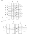
- FIG. 1 is a diagram schematically showing a configuration example of a semiconductor laser optical device according to the first embodiment of the present invention.
- 1A is a plan view seen from the fast axis direction
- FIG. 1B is an enlarged view showing a region surrounded by a broken-line circle in FIG.
- FIG. 2 is a plan view of the semiconductor laser optical device shown in FIG. 1 viewed from the slow axis direction.
- the semiconductor laser optical device includes a laser light source 10 including a semiconductor laser element 11, a first collimating lens 20 provided on the laser light emitting side of the laser light source 10, and an emitting side of the first collimating lens 20.
- the second collimating lens 30 is provided.
- the first collimating lens 20 has a function of collimating a light component that diverges in the fast axis direction (Y-axis direction) of laser light emitted from the laser light source 10 (indicated by a two-dot chain line in FIGS. 1 and 2).
- the second collimating lens 30 has a function of collimating a light component that diverges in the slow axis direction (X-axis direction) of the light emitted from the first collimating lens 20.
- the laser light source 10 includes, for example, a semiconductor laser element 11 in which a plurality of (in this example, five) emitters 12 each wide in the slow axis direction are arranged in a line at a predetermined interval in the slow axis direction.
- the semiconductor laser element 11 is, for example, of an end face emission type.
- the laser beam is in the slow axis direction with respect to the optical axis (indicated by a one-dot chain line) C of the emitter 12 from one end surface of each emitter 12 perpendicular to the pn junction surface of the semiconductor laser element 11.
- the light is emitted with a predetermined divergence angle in the fast axis direction.
- a configuration example of the semiconductor laser element 11 is 4 mm ⁇ 0.1 mm ⁇ 1.5 mm (X-axis direction ⁇ Y-axis direction ⁇ Z-axis direction), and laser light from one emitter 12 is emitted.
- the dimension of one end surface (laser beam emitting end surface) is 40 ⁇ m ⁇ 1 ⁇ m (X-axis direction ⁇ Y-axis direction).
- the center distance (arrangement pitch) p between adjacent emitters is 200 ⁇ m
- the oscillation wavelength is 634 to 644 nm
- the divergence angle in the fast axis direction with respect to the optical axis is 40 ° in full width at half maximum
- the divergence angle in the slow axis direction is full width at half maximum. It is 7 °.
- the first collimating lens 20 emits a light component of the laser light emitted from the emitter 12 in the semiconductor laser element 11 that diverges in the fast axis direction with respect to the optical axis C of the emitter 12 to the optical axis C side of the emitter 12. It has a function of collimating in the fast axis direction by deflecting to the right. That is, the first collimating lens 20 collimates the laser light emitted from the emitter 12 with respect to the optical axis of the emitter 12 in the YZ plane.
- the first collimating lens 20 is disposed close to the laser light source 10 with the optical axis coinciding with the optical axis of the semiconductor laser element 11.
- the second collimating lens 30 converts the light component of the laser beam emitted from the first collimating lens 20 that diverges in the slow axis direction with respect to the optical axis of the emitter 12 into the light of the emitter 12. It has a function of collimating in the slow axis direction by deflecting toward the axis C side. That is, the second collimating lens 30 collimates the laser light emitted from the first collimating lens 20 collimated in the fast axis direction with respect to the optical axis of the emitter 12 in the XZ plane.
- the second collimating lens 30 in this example is configured by, for example, a plurality of lens elements 31 corresponding to each of the plurality of emitters 12 in the semiconductor laser element 11 being arranged in the slow axis direction.
- the entrance surface 32 of each lens element 31 is disposed to face the exit surface 27 of the first collimator lens 20 in a state where the optical axis of the second collimator lens 30 coincides with the optical axis of the semiconductor laser element 11. Yes.
- Each lens element 31 is made of a plano-convex cylindrical lens having a refracting surface composed of a convex cylindrical surface on the first collimating lens 20 side, for example, and the flat surface is configured as the exit surface 35.
- the first collimating lens 20 constituting the semiconductor laser optical device has a function of causing the light that has been prevented from spreading in the slow axis direction to enter the second collimating lens 30 (hereinafter referred to as “slow axis direction deflection”). Correction function ”).
- the first collimating lens 20 in this example has a spread suppressing function portion 25 in the side edge region in the slow axis direction on the incident surface 22 of the laser light emitted from each emitter 12.
- the first collimating lens 20 has a V-shaped groove portion in the XZ plane in each region facing the region between adjacent emitters on the flat surface of the plano-convex cylindrical lens. It is formed so as to extend parallel to each other in the direction.
- each deflection correction lens portion 21 is arranged side by side as an example in the slow axis direction for each emitter 12. Further, the spread suppressing function portion 25 is configured by the concave inclined surface 22A of each deflection correction lens portion 21.
- the dimension in the slow axis direction of one deflection correction lens portion 21 is configured to be smaller than the arrangement pitch p of the emitters 12 in the slow axis direction centered on the optical axis C of the emitter 12, for example.
- the light component that travels while being diverged at a relatively large divergence angle in the slow axis direction is a deflection correction corresponding to the emitter 12.
- the light enters the concave inclined surface 22A of the lens portion 21.
- the high angle light component incident on the concave inclined surface 22A is deflected to the optical axis C side of the emitter 12, and is emitted as a low angle light component in which the divergence angle in the slow axis direction is suppressed to be small.
- the “high angle light component” means a light component that diverges at an angle exceeding ⁇ 5.8 ° with respect to the optical axis C of the emitter 12
- the “low angle light component” means A light component that diverges at an angle within a range of ⁇ 5.8 ° with respect to the optical axis C of the emitter 12.
- each deflection correction lens portion 21 allows the laser light from each emitter 12 to enter the corresponding lens element 31 of the second collimating lens 30 and to be emitted from the second collimating lens 30.
- the laser light related to each emitter 12 has an inclination angle that is substantially parallel to the optical axis C of the emitter 12.
- the inclination angle of the concave inclined surface 22A in each deflection correction lens portion 21 will be specifically described with reference to FIG.
- the inclination angle of the concave inclined surface 22A in the deflection correction lens portion 21 is the sign (the direction of the arrow) of the inclination of the incident light angle ⁇ 1 with respect to the concave inclined surface 22A in the plane (XZ plane) viewed from the fast axis direction.
- the angle of the light beam incident on the incident surface 32 of the corresponding lens element 31 of the second collimating lens 30 is set in an angle range in which the signs of the inclinations coincide.
- B the laser light emitted from the second collimating lens 30 does not become light parallel to the optical axis C of the emitter 12.
- FIG. 4-C it cannot enter the corresponding lens element 31 in the second collimating lens 30 and crosstalk light is generated.
- FIG. 4-C as a comparative example, even when the incident surface 22 of the first collimating lens 20 is a flat surface, the configuration is the same as that shown in FIG. 4-B.
- the sign of the slope is different. Thereby, it cannot enter into the corresponding lens element 31 in the 2nd collimating lens 30, and will become crosstalk light.
- the separation distance in the optical axis direction (Z-axis direction) between the flat surface on the incident surface 22 of the first collimating lens 20 and the end surface from which the laser light of the emitter 12 is emitted is 0.16 mm.
- the dimension of the first collimating lens 20 in the optical axis direction is 1 mm, and the refractive index of the first collimating lens 20 is 1.78.
- the minimum separation distance in the optical axis direction (Z-axis direction) between the incident surface 32 of each lens element 31 of the second collimating lens 30 and the emission surface 27 of the first collimating lens 20 is set to 0.4 mm.
- each lens element 31 of the second collimating lens 30 is 0.81 mm
- the refractive index of the second collimating lens 30 is 1.81
- the light enters the concave inclined surface 22A of the first collimating lens 20.
- the light beam angle ⁇ 1 is set to 7.5 to 10.8 °.
- the inclination angle of the concave inclined surface 22A forming the spread suppressing function portion 25 is within an angle range of 5 ° or less.
- the laser light source 10 including the semiconductor laser element 11 in which the plurality of emitters 12 are arranged in a line in the slow axis direction is arranged.
- the first collimating lens 20 includes a plurality of deflection correction lens portions each having a spread suppressing function portion 25 in a side edge region in the slow axis direction on the incident surface 22 of the laser light emitted from the emitter 12 in the semiconductor laser element 11. 21 is arranged in a line in the slow axis direction.
- the high-angle light component that diverges at a large divergence angle that can be crosstalk light is emitted by the spread suppression function portion 25. It is possible to correct the deflection toward the 12 optical axis C side. Therefore, the laser light emitted from the first collimating lens 20 can be collimated in the slow axis direction by the second collimating lens 30. That is, the spread in the slow axis direction is suppressed by the spread suppressing function portion 25 in each deflection correction lens portion 21 of the first collimating lens 20.
- the laser light emitted from the first collimating lens 20 can be reliably incident on the corresponding lens element 31 in the second collimating lens 30 and collimated in the slow axis direction by the lens action of the lens element 31. can do. Therefore, according to the semiconductor laser optical device configured as described above, generation of crosstalk light can be reliably suppressed, high collimation efficiency can be obtained, and light utilization can be improved. In addition, it is not necessary to use another optical member such as a beam splitter or a deflection mechanism in order to improve the collimating property. For this reason, it is possible to manufacture a device having the desired performance with a small number of parts in an advantageous cost, and the semiconductor laser optical device itself can be configured to be small.
- FIG. 5 is a diagram schematically showing a configuration example of a semiconductor laser optical device according to the second embodiment of the present invention.
- FIG. 5A is a plan view seen from the fast axis direction
- FIG. 5B is an enlarged view showing a region surrounded by a broken-line circle in FIG.
- the semiconductor laser optical device according to the second embodiment is the same as the first collimator lens 20 in the semiconductor laser optical device according to the first embodiment described above, on the side in the slow axis direction on both the entrance surface and the exit surface.
- the semiconductor laser optical device according to the first embodiment has the same configuration as that of the semiconductor laser optical device according to the first embodiment, except that an edge region having a spread suppressing function portion is used.
- FIG. 5 for the sake of convenience, the same components as those in the semiconductor laser optical device according to the first embodiment are denoted by the same reference numerals.
- each of the regions facing the region between adjacent emitters on the flat surface of the plano-convex cylindrical lens on the plane (XZ plane) viewed from the fast axis direction has V V
- the letter-shaped grooves are formed so as to extend in parallel to each other in the fast axis direction.
- a plurality of incident-side deflection correction lens portions 21 ⁇ / b> A having a trapezoidal incident surface 22 that is convex toward the laser light source 10 are formed in a region between adjacent grooves.
- Each incident-side deflection correction lens portion 21 ⁇ / b> A is arranged in one example in the slow axis direction corresponding to each emitter 12.
- V-shaped grooves are formed in the refractive surface of the plano-convex cylindrical lens so as to extend in parallel with each other in the fast axis direction at positions facing each of the grooves.
- a plurality of exit-side deflection correction lens portions 26 each having a trapezoidal exit surface 27 convex toward the second collimating lens 30 are formed in a region between adjacent grooves.
- Each exit-side deflection correction lens portion 26 is arranged in an example in the slow axis direction corresponding to each emitter 12. Accordingly, in the first collimating lens 20, the first spread suppressing functional portion 25A is configured by the concave inclined surface 22A of each incident side deflection correction lens portion 21A, and each emission side deflection correction lens portion 26 is formed.
- the second spread suppressing functional portion 25B is configured by the convex inclined surface 27A.
- the concave inclined surface 22A in the incident-side deflection correction lens portion 21A and the convex inclined surface 27A in the emission-side deflection correction lens portion 26 are formed at different inclination angles even if they are formed at the same inclination angle. Also good.
- the light component that travels while diverging at a large divergence angle in the slow axis direction corresponds to the emitter 12 in the first collimating lens 20.
- the high-angle light component incident on the concave inclined surface 22A is deflected to the optical axis C side of the emitter 12 by the action of the first spread suppressing functional portion 25A. Therefore, according to such a configuration, when the light component is emitted from the convex inclined surface 27A of the emission side deflection correction lens portion 26, the deflection correction can be further made to the optical axis C side of the emitter 12.
- the action of the second spread suppression function portion 25B the light that could not be deflected by the first spread suppression function portion 25A can be corrected again, and the lens design for improving collimation is free. The degree can be increased.
- FIG. 6 is a diagram schematically showing a configuration example of a semiconductor laser optical device according to the third embodiment of the present invention.
- 6A is a plan view seen from the fast axis direction
- FIG. 6B is an enlarged view showing a region surrounded by a broken-line circle in FIG. 6A.
- the semiconductor laser optical device according to the third embodiment has a slow axis direction deflection correction function using reflection as the first collimating lens 20 in the semiconductor laser optical device according to the first embodiment. Except that is used, the semiconductor laser optical device according to the first embodiment has the same configuration.
- FIG. 6 for the sake of convenience, the same components as those in the semiconductor laser optical device according to the first embodiment are denoted by the same reference numerals.
- each of the regions facing the region between adjacent emitters on the flat surface of the plano-convex cylindrical lens on the plane (XZ plane) viewed from the fast axis direction Trapezoidal notches that are convex toward the second collimating lens 30 in the axial direction are formed so as to extend parallel to each other in the slow axis direction.
- a plurality of frustum-shaped deflection correction lens portions 21 are formed in a region between adjacent cutout portions.
- Each deflection correction lens portion 21 is arranged side by side in the slow axis direction corresponding to each of the emitters 12.
- the flat surface of each deflection correction lens portion 21 is an incident surface 22 on which the laser beam from the emitter 12 is incident.
- each deflection correction lens portion 21 is a high-angle light component that diverges at a relatively large divergence angle in the slow axis direction, out of the laser light from the emitter 12 incident from the flat surface of the deflection correction lens portion 21. Is formed at an inclination angle at which critical reflection (total reflection) occurs. Accordingly, the first collimating lens 20 performs the deflection correction to the optical axis C side of the emitter 12 in the slow axis direction by totally reflecting the high angle light component by the inner surface 23 in the deflection correction lens portion 21. It is configured to have a deflection correction function.
- FIG. 7 is a diagram schematically showing a configuration example of a semiconductor laser optical device according to the fourth embodiment of the present invention.
- FIG. 7A is a plan view seen from the fast axis direction
- FIG. 7B is an enlarged view showing a region surrounded by a broken-line circle in FIG. 7A.
- the semiconductor laser optical device according to the fourth embodiment has a slow axis direction deflection correction function using reflection as the first collimating lens 20 in the semiconductor laser optical device according to the first embodiment. Except that is used, the semiconductor laser optical device according to the first embodiment has the same configuration.
- FIG. 7 for the sake of convenience, the same components as those of the semiconductor laser optical device according to the first embodiment are denoted by the same reference numerals.
- each of the regions facing the region between adjacent emitters on the flat surface of the planoconvex cylindrical lens on the plane (XZ plane) viewed from the fast axis direction Trapezoidal concave portions 28 that protrude toward the axial laser light source side are formed so as to extend parallel to each other in the slow axis direction.
- a reflective film 29 is formed on the inclined inner side surface 28A of the concave portion 28, and the flat inner end surface of each concave portion 28 is an incident surface 22 on which laser light from the emitter is incident.
- the first collimating lens 20 In the first collimating lens 20, the high-angle light component that diverges at a relatively large divergence angle in the slow axis direction out of the laser light from the emitter 12 that enters the recess 28 through the opening of the recess 28. Is reflected by the reflective film 29. Accordingly, the first collimating lens 20 is configured to have a slow axis direction deflection correction function for correcting the deflection of the high angle light component toward the optical axis C of the emitter 12 in the slow axis direction.
- the inclination angle of the inner side surface 28 ⁇ / b> A of each concave portion 28 is the sign of the inclination of the ray angle incident on the inner end surface of the concave portion 28 as the incident surface 22 and the incident surface 32 of the corresponding lens element 31 of the second collimating lens 30. Is set within an angle range in which the signs of the inclinations of the light ray angles incident on the beam coincide.
- the reflective film 29 preferably has a high reflection characteristic (for example, 90% or more) in the wavelength range of the laser light emitted from the semiconductor laser element 11.
- a reflective film 29 can be made of aluminum, for example.
- the thickness of the reflective film 29 is, for example, 100 to 200 ⁇ m.
- the separation distance in the optical axis direction (Z-axis direction) between the flat surface of the first collimating lens 20 where the recess 28 is formed and the end surface from which the laser light of the emitter 12 is emitted is The distance is set smaller than the separation distance in the semiconductor laser optical device according to the first embodiment. This is to ensure that the laser light from the emitter 12 enters the corresponding recess 28 in the first collimating lens 20.
- a semiconductor laser optical device having the following specifications was manufactured according to the configuration shown in FIG. Furthermore, a condensing lens is arranged on the exit side of the second collimating lens, and an optical fiber (outer diameter ⁇ 0.40 mm) is arranged so that its incident end face is positioned at the focal position of the condensing lens, and enters the optical fiber. Measured luminous flux. As a result, it was confirmed that the utilization factor of light was 98.8%.
- the utilization factor of light is indicated by a value obtained by dividing the size of the light beam incident on the optical fiber by the size of the total light beam including the light component not irradiated on the incident surface of the optical fiber.
- the irradiation spot formed on the incident end face of the optical fiber had a dimension in the fast axis direction of ⁇ 0.08 mm and a dimension in the slow axis direction of ⁇ 0.2 mm. From this result, it was confirmed that the same collimating property was obtained in the fast axis direction and the slow axis direction.
- the semiconductor laser optical according to the present invention has the same configuration as that of Experimental Example 1 except that the first collimating lens having the configuration shown in FIG. 6 is used.
- a device was made.
- This first collimating lens has the following specifications.
- the light utilization factor was determined by the same method as in Experimental Example 1, and it was confirmed that it was 96%.
- the irradiation spot formed on the incident end face of the optical fiber had a dimension in the fast axis direction of 0.08 mm and a dimension in the slow axis direction of 0.2 mm. From this result, it was confirmed that the same collimating property was obtained in the fast axis direction and the slow axis direction.
- the semiconductor laser optical according to the present invention has the same configuration as that of Experimental Example 1 except that the first collimating lens has the configuration shown in FIG. A device was made.
- This first collimating lens has the following specifications.
- the light utilization factor was determined by the same method as in Experimental Example 1, and it was confirmed that it was 95%.
- the irradiation spot formed on the incident end face of the optical fiber had a dimension in the fast axis direction of 0.08 mm and a dimension in the slow axis direction of 0.2 mm. From this result, it was confirmed that the same collimating property was obtained in the fast axis direction and the slow axis direction.
- the semiconductor laser optical device of the present invention it has been confirmed that a high light utilization rate can be obtained as compared with the semiconductor laser optical device for comparison, and therefore high collimation efficiency can be obtained. It was.
- the spread suppressing function portion in the semiconductor laser optical device according to the first embodiment and the first spread suppressing function portion in the semiconductor laser optical device according to the second embodiment may be configured by convex inclined surfaces.
- the second spread suppressing functional portion in the semiconductor laser optical device according to the second embodiment may be configured by a concave inclined surface.
- the laser light source is not limited to an array type in which a plurality of emitters are arranged in a line in the slow axis direction.
- a plurality of chip-shaped semiconductor laser elements in which a plurality of emitters are arranged in a line in the slow axis direction may be stacked in the fast axis direction.
Landscapes
- Physics & Mathematics (AREA)
- General Physics & Mathematics (AREA)
- Optics & Photonics (AREA)
- Condensed Matter Physics & Semiconductors (AREA)
- Electromagnetism (AREA)
- Semiconductor Lasers (AREA)
- Lenses (AREA)
Abstract
本発明は、クロストーク光の発生が抑制されて高いコリメート効率が得られ、しかも比較的安価で、コンパクトな半導体レーザ光学装置を提供することを目的とする。 この半導体レーザ光学装置は、半導体レーザ素子を備えたレーザ光源と、レーザ光源のレーザ光出射側に設けられた、レーザ光源から出射されるレーザ光のファスト軸方向に発散する光成分をコリメートする第1のコリメートレンズと、第1のコリメートレンズの出射側に設けられた、第1のコリメートレンズから出射された光のスロー軸方向に発散する光成分をコリメートする第2のコリメートレンズとを具備し、第1のコリメートレンズは、スロー軸方向に対する広がりが抑制された光を、第2のコリメートレンズに入射させる機能を有する。
Description
本発明は、半導体レーザ光学装置に関する。さらに詳しくは、例えば、高出力のアレイ型半導体レーザ素子を備えたレーザ光源から出射されるレーザ光を、効率良くコリメートすることのできるコリメートレンズ構造体を備えた半導体レーザ光学装置に関する。
レーザ光源としては、例えば半導体レーザ素子から出射される光を適宜の光学部材によって集光して細径な光ファイバのコア部に効率良く入射させるために、コリメート性(平行性)の高いビームを出射することのできるものであることが望まれている。
半導体レーザ素子としては、例えば、複数のエミッタが配置されたアレイ型のものが知られている。アレイ型の半導体レーザ素子は、一般的には、端面放射タイプのものとして構成されており、例えば数W以上の光出力が求められている。
このような半導体レーザ素子によれば、pn接合面に垂直な方向であるファスト軸方向においては、活性層の厚みすなわち各エミッタのファスト軸方向寸法が十分に小さいことから、広がりの大きいシングルモードの光が出射される。これに対して、pn接合面に対して平行な方向であるスロー軸方向においては、活性層が幅広なため、すなわち各エミッタのスロー軸方向寸法が大きいため、広がりの小さいマルチモードの光が出射される。従って、スロー軸方向に発散する光成分は、ファスト軸方向に発散する光成分に対してビームの品質が悪く、コリメートしにくい光となっている。
半導体レーザ素子としては、例えば、複数のエミッタが配置されたアレイ型のものが知られている。アレイ型の半導体レーザ素子は、一般的には、端面放射タイプのものとして構成されており、例えば数W以上の光出力が求められている。
このような半導体レーザ素子によれば、pn接合面に垂直な方向であるファスト軸方向においては、活性層の厚みすなわち各エミッタのファスト軸方向寸法が十分に小さいことから、広がりの大きいシングルモードの光が出射される。これに対して、pn接合面に対して平行な方向であるスロー軸方向においては、活性層が幅広なため、すなわち各エミッタのスロー軸方向寸法が大きいため、広がりの小さいマルチモードの光が出射される。従って、スロー軸方向に発散する光成分は、ファスト軸方向に発散する光成分に対してビームの品質が悪く、コリメートしにくい光となっている。
このようなアレイ型の半導体レーザ素子を備えたレーザ光源から出射されたレーザ光をコリメートする技術としては、例えば図8に示すような技術が知られている。図8では、複数のエミッタ12がスロー軸方向(X軸方向)に一列に並んで配置された半導体レーザ素子11から出射されるレーザ光のファスト軸方向(紙面に垂直な方向,Y軸方向)に発散する光成分をファスト軸方向コリメートレンズ40によってコリメートしている。更に、このファスト軸方向コリメートレンズ40から出射された光のスロー軸方向(X軸方向)に発散する光成分をスロー軸方向コリメートレンズ50によってコリメートしている。ここに、スロー軸方向コリメートレンズ50としては、例えば、半導体レーザ素子11における各々のエミッタ12に対応する複数のレンズ要素51がスロー軸方向(X軸方向)に一列に並んで配置された構造のものが用いられている。図8における符号Cは、エミッタ12の光軸である。
また、スロー軸方向のコリメート性を向上させるための方法として、例えば、ファスト軸方向コリメートレンズとスロー軸方向コリメートレンズとの間に、ファスト軸方向にビームを分割する手段を設ける技術が知られている(特許文献1参照。)。
また、スロー軸方向のコリメート性を向上させるための方法として、例えば、ファスト軸方向コリメートレンズとスロー軸方向コリメートレンズとの間に、ファスト軸方向にビームを分割する手段を設ける技術が知られている(特許文献1参照。)。
しかしながら、ファスト軸方向コリメートレンズ40とスロー軸方向コリメートレンズ50とを並べた構成のものにおいては、以下の問題がある。すなわち、図8(b)に示すように、ファスト軸方向から見た平面(X-Z平面)において、半導体レーザ素子11における一のエミッタ12に対面して配置された、スロー軸方向コリメートレンズ50における当該エミッタ12に対応するレンズ要素51bに入射されるレーザ光が、隣接するレンズ要素51a、51cに入射してしまう。図8(a)、(b)において二点鎖線で示すように、比較的低角度成分の光は、所定のレンズ要素51bに入射されてスロー軸方向にコリメートされる。しかし、図8(a)、(b)において破線で示すように、比較的高角度成分の光は、所定のレンズ要素51の両側に隣接するレンズ要素51a,51cに入射されるため、スロー軸方向コリメートレンズ50から出射される光は発散(以後、「クロストーク」と称する。)してしまう、といった問題がある。
また、半導体レーザ素子11が、複数のエミッタ12がスロー軸方向に所定の間隔で一列に並んで配置された構成とされていることから、スロー軸方向のコリメートを効率良く実施するためには、以下の配置とする必要がある。すなわち、スロー軸方向コリメートレンズ50を、各レンズ要素51における入射面が互いに隣接するエミッタ12の各々から出射されたレーザ光がファスト軸方向コリメートレンズ40から出射された後に、当該レーザ光が重なる位置より当該スロー軸方向コリメートレンズ50を半導体レーザ素子11側に配置することが必要とされる。しかしながら、このような位置関係においては、スロー軸方向のコリメート性がファスト軸方向のコリメート性より劣るものとなってしまう、といった問題がある。
また、半導体レーザ素子11が、複数のエミッタ12がスロー軸方向に所定の間隔で一列に並んで配置された構成とされていることから、スロー軸方向のコリメートを効率良く実施するためには、以下の配置とする必要がある。すなわち、スロー軸方向コリメートレンズ50を、各レンズ要素51における入射面が互いに隣接するエミッタ12の各々から出射されたレーザ光がファスト軸方向コリメートレンズ40から出射された後に、当該レーザ光が重なる位置より当該スロー軸方向コリメートレンズ50を半導体レーザ素子11側に配置することが必要とされる。しかしながら、このような位置関係においては、スロー軸方向のコリメート性がファスト軸方向のコリメート性より劣るものとなってしまう、といった問題がある。
さらにまた、上述の特許文献1に記載の技術では、互いに隣接するエミッタの各々から出射されたレーザ光がファスト軸方向コリメートレンズによってコリメートされて当該ファスト軸方向コリメートレンズからファスト軸方向の高さを変えて出射される。各エミッタからの光は、スロー軸方向に出射される光の重なりが生じないため、スロー軸方向コリメートレンズのレンズ径を隣接するエミッタから出射されるレーザ光の重なりを考慮せずに設定することができるといった利点がある。しかしながら、光学系が複雑で、それ自身が比較的大きな構造のものとなってしまう、といった問題がある。
本発明は、以上のような事情に基づいてなされたものであり、クロストーク光の発生を抑制することができて高いコリメート効率を得ることができ、しかも比較的安価に作製することができて、コンパクトな半導体レーザ光学装置を提供することを目的とする。
本発明の半導体レーザ光学装置は、半導体レーザ素子よりなるレーザ光源と、当該レーザ光源のレーザ光出射側に設けられた、当該レーザ光源から出射されるレーザ光のファスト軸方向に発散する光成分をコリメートする第1のコリメートレンズと、当該第1のコリメートレンズの出射側に設けられた、当該第1のコリメートレンズから出射された光のスロー軸方向に発散する光成分をコリメートする第2のコリメートレンズとを具備した半導体レーザ光学装置において、
前記第1のコリメートレンズは、スロー軸方向に対する広がりが抑制された光を前記第2のコリメートレンズに入射させる機能を有することを特徴とする。
前記第1のコリメートレンズは、スロー軸方向に対する広がりが抑制された光を前記第2のコリメートレンズに入射させる機能を有することを特徴とする。
本発明の半導体レーザ光学装置においては、前記第1のコリメートレンズは、入射面および出射面のいずれか一方または両方におけるスロー軸方向の側縁領域に広がり抑制機能部分を有するものとすることができる。
また、本発明の半導体レーザ光学装置においては、前記レーザ光源を構成する半導体レーザ素子として、複数のエミッタが一列に並んで配置されているものを用いることができる。
本発明の半導体レーザ光学装置においては、レーザ光源から出射されるレーザ光のファスト軸方向に発散する光成分をコリメートする第1のコリメートレンズが、スロー軸方向に対する広がりが抑制された光を第2のコリメートレンズに入射させる機能を有する。従って、本発明の半導体レーザ光学装置によれば、スロー軸方向に発散する光成分のうち、クロストーク光と成りうる大きな発散角度で発散する光成分を光軸側に偏向補正することができる。更に、第1のコリメートレンズより出射されるレーザ光は、第2のコリメートレンズによってスロー軸方向に十分なコリメートをすることのできるものとなる。従って、クロストーク光の発生が抑制されて高いコリメート効率が得られる。しかも、コリメート性を向上させるために、例えばビームスプリッターや偏向機構などの他の光学部材を用いる必要がないので、所期の性能を有するものを少ない部品点数でコスト的に有利に作製することができると共に、装置自体を小型のものとして構成することができる。
以下、本発明の実施の形態について詳細に説明する。
<第1の実施形態>
図1は、本発明の第1の実施形態に係る半導体レーザ光学装置の一構成例を概略的に示す図である。図1(a)は、ファスト軸方向から見た平面図であり、図1(b)は、図1(a)における破線の円で囲まれた領域を示す拡大図である。図2は、図1に示す半導体レーザ光学装置をスロー軸方向から見た平面図である。
この半導体レーザ光学装置は、半導体レーザ素子11を備えたレーザ光源10と、このレーザ光源10のレーザ光出射側に設けられた第1のコリメートレンズ20と、この第1のコリメートレンズ20の出射側に設けられた第2のコリメートレンズ30とを具備している。第1のコリメートレンズ20は、レーザ光源10から出射されるレーザ光(図1および図2において二点鎖線で示す。)のファスト軸方向(Y軸方向)に発散する光成分をコリメートする機能を有する。第2のコリメートレンズ30は、第1のコリメートレンズ20から出射された光のスロー軸方向(X軸方向)に発散する光成分をコリメートする機能を有する。
図1は、本発明の第1の実施形態に係る半導体レーザ光学装置の一構成例を概略的に示す図である。図1(a)は、ファスト軸方向から見た平面図であり、図1(b)は、図1(a)における破線の円で囲まれた領域を示す拡大図である。図2は、図1に示す半導体レーザ光学装置をスロー軸方向から見た平面図である。
この半導体レーザ光学装置は、半導体レーザ素子11を備えたレーザ光源10と、このレーザ光源10のレーザ光出射側に設けられた第1のコリメートレンズ20と、この第1のコリメートレンズ20の出射側に設けられた第2のコリメートレンズ30とを具備している。第1のコリメートレンズ20は、レーザ光源10から出射されるレーザ光(図1および図2において二点鎖線で示す。)のファスト軸方向(Y軸方向)に発散する光成分をコリメートする機能を有する。第2のコリメートレンズ30は、第1のコリメートレンズ20から出射された光のスロー軸方向(X軸方向)に発散する光成分をコリメートする機能を有する。
レーザ光源10は、例えば、各々スロー軸方向に幅広な複数(この例では5つ)のエミッタ12がスロー軸方向に所定の間隔で一列に並んで配置された半導体レーザ素子11を備えてなる。
半導体レーザ素子11は、例えば端面放射タイプのものである。この半導体レーザ素子11においては、各エミッタ12における、半導体レーザ素子11のpn接合面に垂直な一端面より、レーザ光がエミッタ12の光軸(一点鎖線で示す。)Cに対してスロー軸方向およびファスト軸方向に所定の発散角度をもって出射される。
半導体レーザ素子11の一構成例を示すと、外形寸法が4mm×0.1mm×1.5mm(X軸方向×Y軸方向×Z軸方向)であり、一のエミッタ12におけるレーザ光が出射される一端面(レーザ光出射端面)の寸法が40μm×1μm(X軸方向×Y軸方向)である。また、隣接するエミッタの中心間距離(配設ピッチ)pが200μm、発振波長が634~644nm、光軸に対するファスト軸方向の発散角度が半値全角で40°、スロー軸方向の発散角度が半値全角で7°である。
半導体レーザ素子11は、例えば端面放射タイプのものである。この半導体レーザ素子11においては、各エミッタ12における、半導体レーザ素子11のpn接合面に垂直な一端面より、レーザ光がエミッタ12の光軸(一点鎖線で示す。)Cに対してスロー軸方向およびファスト軸方向に所定の発散角度をもって出射される。
半導体レーザ素子11の一構成例を示すと、外形寸法が4mm×0.1mm×1.5mm(X軸方向×Y軸方向×Z軸方向)であり、一のエミッタ12におけるレーザ光が出射される一端面(レーザ光出射端面)の寸法が40μm×1μm(X軸方向×Y軸方向)である。また、隣接するエミッタの中心間距離(配設ピッチ)pが200μm、発振波長が634~644nm、光軸に対するファスト軸方向の発散角度が半値全角で40°、スロー軸方向の発散角度が半値全角で7°である。
第1のコリメートレンズ20は、半導体レーザ素子11におけるエミッタ12から出射されるレーザ光の、エミッタ12の光軸Cに対してファスト軸方向に発散する光成分を、当該エミッタ12の光軸C側に偏向することによりファスト軸方向にコリメートする機能を有している。すなわち、第1のコリメートレンズ20は、エミッタ12から出射されるレーザ光を、Y-Z平面においてエミッタ12の光軸に対して平行光化する。
この第1のコリメートレンズ20は、光軸が半導体レーザ素子11の光軸と一致する状態で、レーザ光源10に近接して配置されている。
この第1のコリメートレンズ20は、光軸が半導体レーザ素子11の光軸と一致する状態で、レーザ光源10に近接して配置されている。
第2のコリメートレンズ30は、第1のコリメートレンズ20から出射される各エミッタ12に係るレーザ光の、エミッタ12の光軸に対してスロー軸方向に発散する光成分を、当該エミッタ12の光軸C側に偏向することによりスロー軸方向にコリメートする機能を有している。すなわち、第2のコリメートレンズ30は、ファスト軸方向にコリメートされた第1のコリメートレンズ20から出射されるレーザ光を、X-Z平面においてエミッタ12の光軸に対して平行光化する。
この例における第2のコリメートレンズ30は、例えば半導体レーザ素子11における複数のエミッタ12の各々に対応する複数のレンズ要素31がスロー軸方向に並んで配置されて構成されている。各レンズ要素31の入射面32は、第2のコリメートレンズ30の光軸が半導体レーザ素子11の光軸と一致する状態で、第1のコリメートレンズ20の出射面27に対向して配置されている。また、各々のレンズ要素31は、例えば、第1のコリメートレンズ20側に凸の円柱面よりなる屈折面を有する平凸シリンドリカルレンズよりなり、平坦面が出射面35として構成されている。
この例における第2のコリメートレンズ30は、例えば半導体レーザ素子11における複数のエミッタ12の各々に対応する複数のレンズ要素31がスロー軸方向に並んで配置されて構成されている。各レンズ要素31の入射面32は、第2のコリメートレンズ30の光軸が半導体レーザ素子11の光軸と一致する状態で、第1のコリメートレンズ20の出射面27に対向して配置されている。また、各々のレンズ要素31は、例えば、第1のコリメートレンズ20側に凸の円柱面よりなる屈折面を有する平凸シリンドリカルレンズよりなり、平坦面が出射面35として構成されている。
而して、上記の半導体レーザ光学装置を構成する第1のコリメートレンズ20は、スロー軸方向に対する広がりが抑制された光を第2のコリメートレンズ30に入射させる機能(以下、「スロー軸方向偏向補正機能」という。)を有する。
この例における第1のコリメートレンズ20は、各エミッタ12から出射されたレーザ光の入射面22におけるスロー軸方向の側縁領域に、広がり抑制機能部分25を有する。具体的には、第1のコリメートレンズ20は、X-Z平面において、平凸シリンドリカルレンズの平坦面における、隣接するエミッタ間の領域に対面する領域の各々に、V字型の溝部がファスト軸方向に互いに平行に延びるよう形成されている。これにより、隣接する溝部間の領域に、各々台形状の入射面22を有する複数の偏向補正レンズ部分21が形成されている。各偏向補正レンズ部分21は、エミッタ12の各々にしてスロー軸方向に一例に並んで配置されている。
また、各々の偏向補正レンズ部分21の凹状傾斜面22Aによって広がり抑制機能部分25が構成されている。ここに、一の偏向補正レンズ部分21のスロー軸方向の寸法は、例えばエミッタ12の光軸Cを中心としたスロー軸方向におけるエミッタ12の配設ピッチpより小さく構成される。
この第1のコリメートレンズ20においては、一のエミッタ12から出射されるレーザ光のうち、スロー軸方向に比較的大きな発散角で発散されながら進行する光成分は、当該エミッタ12に対応する偏向補正レンズ部分21の凹状傾斜面22Aに入射される。この凹状傾斜面22Aに入射される高角度光成分が当該エミッタ12の光軸C側に偏向されて、スロー軸方向における発散角が小さく抑制された低角度光成分として出射される。ここに、スロー軸方向において、「高角度光成分」とは、エミッタ12の光軸Cに対して±5.8°を超える角度で発散する光成分をいい、「低角度光成分」とはエミッタ12の光軸Cに対して±5.8°の範囲内の角度で発散する光成分をいう。
この例における第1のコリメートレンズ20は、各エミッタ12から出射されたレーザ光の入射面22におけるスロー軸方向の側縁領域に、広がり抑制機能部分25を有する。具体的には、第1のコリメートレンズ20は、X-Z平面において、平凸シリンドリカルレンズの平坦面における、隣接するエミッタ間の領域に対面する領域の各々に、V字型の溝部がファスト軸方向に互いに平行に延びるよう形成されている。これにより、隣接する溝部間の領域に、各々台形状の入射面22を有する複数の偏向補正レンズ部分21が形成されている。各偏向補正レンズ部分21は、エミッタ12の各々にしてスロー軸方向に一例に並んで配置されている。
また、各々の偏向補正レンズ部分21の凹状傾斜面22Aによって広がり抑制機能部分25が構成されている。ここに、一の偏向補正レンズ部分21のスロー軸方向の寸法は、例えばエミッタ12の光軸Cを中心としたスロー軸方向におけるエミッタ12の配設ピッチpより小さく構成される。
この第1のコリメートレンズ20においては、一のエミッタ12から出射されるレーザ光のうち、スロー軸方向に比較的大きな発散角で発散されながら進行する光成分は、当該エミッタ12に対応する偏向補正レンズ部分21の凹状傾斜面22Aに入射される。この凹状傾斜面22Aに入射される高角度光成分が当該エミッタ12の光軸C側に偏向されて、スロー軸方向における発散角が小さく抑制された低角度光成分として出射される。ここに、スロー軸方向において、「高角度光成分」とは、エミッタ12の光軸Cに対して±5.8°を超える角度で発散する光成分をいい、「低角度光成分」とはエミッタ12の光軸Cに対して±5.8°の範囲内の角度で発散する光成分をいう。
各々の偏向補正レンズ部分21における凹状傾斜面22Aは、各エミッタ12からのレーザ光が第2のコリメートレンズ30の対応するレンズ要素31に入射され、かつ、第2のコリメートレンズ30より出射される各エミッタ12に係るレーザ光がエミッタ12の光軸Cに略平行とされる傾斜角度を有する。
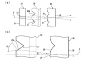
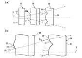
各々の偏向補正レンズ部分21における凹状傾斜面22Aの傾斜角度について、図3を用いて具体的に説明する。偏向補正レンズ部分21における凹状傾斜面22Aの傾斜角度は、ファスト軸方向から見た平面(X-Z平面)において、凹状傾斜面22Aに対する入射する光線角度θ1の傾きの符号(矢印の向き)と、第2のコリメートレンズ30の対応するレンズ要素31の入射面32に入射する光線角度θ2の傾きの符号が一致する角度範囲で設定されている。
凹状傾斜面22Aに入射する光線角度θ1の傾きの符号と、第2のコリメートレンズ30のレンズ要素31に入射する光線角度θ2の傾きの符号が異なる場合には、図4-Aおよび図4-Bに比較例として示すように、第2のコリメートレンズ30から出射されるレーザ光はエミッタ12の光軸Cに平行な光とはならない。特に、図4-Bに示す構成のものにおいては、第2のコリメートレンズ30における対応するレンズ要素31に入射させることができず、クロストーク光となってしまう。なお、図4-Cに比較例として示すように、第1のコリメートレンズ20における入射面22が平坦面である場合においても図4-Bに示す構成のものと同様となる。すなわち、第1のコリメートレンズ20の平坦な入射面22に入射する光線角度θ1の傾きの符号(矢印の向き)と、第2のコリメートレンズ30の対応するレンズ要素31に入射する光線角度θ2の傾きの符号が異なる。これにより、第2のコリメートレンズ30における対応するレンズ要素31に入射させることができず、クロストーク光となってしまう。
凹状傾斜面22Aに入射する光線角度θ1の傾きの符号と、第2のコリメートレンズ30のレンズ要素31に入射する光線角度θ2の傾きの符号が異なる場合には、図4-Aおよび図4-Bに比較例として示すように、第2のコリメートレンズ30から出射されるレーザ光はエミッタ12の光軸Cに平行な光とはならない。特に、図4-Bに示す構成のものにおいては、第2のコリメートレンズ30における対応するレンズ要素31に入射させることができず、クロストーク光となってしまう。なお、図4-Cに比較例として示すように、第1のコリメートレンズ20における入射面22が平坦面である場合においても図4-Bに示す構成のものと同様となる。すなわち、第1のコリメートレンズ20の平坦な入射面22に入射する光線角度θ1の傾きの符号(矢印の向き)と、第2のコリメートレンズ30の対応するレンズ要素31に入射する光線角度θ2の傾きの符号が異なる。これにより、第2のコリメートレンズ30における対応するレンズ要素31に入射させることができず、クロストーク光となってしまう。
例えば、第1のコリメートレンズ20の入射面22における平坦面とエミッタ12のレーザ光が出射される端面との光軸方向(Z軸方向)の離間距離を0.16mmとする。また、第1のコリメートレンズ20の光軸方向の寸法を1mm、第1のコリメートレンズ20の屈折率を1.78とする。そして、第2のコリメートレンズ30の各々のレンズ要素31の入射面32と第1のコリメートレンズ20における出射面27との光軸方向(Z軸方向)の最小離間距離を0.4mmとする。また、第2のコリメートレンズ30の各々のレンズ要素31の曲率半径を0.81mm、第2のコリメートレンズ30の屈折率を1.81、第1のコリメートレンズ20における凹状傾斜面22Aに入射する光線角度θ1を7.5~10.8°とする。この場合には、広がり抑制機能部分25を形成する凹状傾斜面22Aの傾斜角度は、5°以内の角度範囲内であることが好ましい。
而して、上記構成の半導体レーザ光学装置においては、複数のエミッタ12がスロー軸方向に一列に並んで配置されてなる半導体レーザ素子11を備えたレーザ光源10が配置されている。このような構成とされていることにより、レーザ光源10から出射されるレーザ光のファスト軸方向に発散する光成分は、第1のコリメートレンズ20によってコリメートされる。この第1のコリメートレンズ20は、各々半導体レーザ素子11におけるエミッタ12から出射されるレーザ光の入射面22におけるスロー軸方向の側縁領域に、広がり抑制機能部分25を有する複数の偏向補正レンズ部分21が、スロー軸方向に一列に並んで配置された構成とされている。これにより、各エミッタ12から出射されるレーザ光のスロー軸方向に発散する光成分のうち、クロストーク光と成りうる大きな発散角度で発散する高角度光成分を、広がり抑制機能部分25によって、エミッタ12の光軸C側に偏向補正することができる。従って、第1のコリメートレンズ20より出射されるレーザ光は、第2のコリメートレンズ30によってスロー軸方向にコリメートすることのできるものとなる。すなわち、第1のコリメートレンズ20の各々の偏向補正レンズ部分21における広がり抑制機能部分25によってスロー軸方向への広がりが抑制される。また、第1のコリメートレンズ20より出射されるレーザ光を、第2のコリメートレンズ30における対応するレンズ要素31に確実に入射させることができて当該レンズ要素31のレンズ作用によってスロー軸方向にコリメートすることができる。
従って、上記構成の半導体レーザ光学装置によれば、クロストーク光の発生を確実に抑制することができて高いコリメート効率を得ることができ、光の利用率を向上させることができる。しかも、コリメート性を向上させるために、例えばビームスプリッターや偏向機構などの他の光学部材を用いる必要がない。このため、所期の性能を有するものを少ない部品点数でコスト的に有利に作製することができると共に、半導体レーザ光学装置自体を小型のものとして構成することができる。
従って、上記構成の半導体レーザ光学装置によれば、クロストーク光の発生を確実に抑制することができて高いコリメート効率を得ることができ、光の利用率を向上させることができる。しかも、コリメート性を向上させるために、例えばビームスプリッターや偏向機構などの他の光学部材を用いる必要がない。このため、所期の性能を有するものを少ない部品点数でコスト的に有利に作製することができると共に、半導体レーザ光学装置自体を小型のものとして構成することができる。
<第2の実施形態>
図5は、本発明の第2の実施形態に係る半導体レーザ光学装置の一構成例を概略的に示す図である。図5(a)は、ファスト軸方向から見た平面図であり、図5(b)は、図5(a)における破線の円で囲まれた領域を示す拡大図である。
この第2の実施形態に係る半導体レーザ光学装置は、上記の第1の実施形態に係る半導体レーザ光学装置において、第1のコリメートレンズ20として、入射面および出射面の両方におけるスロー軸方向の側縁領域に、広がり抑制機能部分を有するものが用いられたことの他は、第1の実施形態に係る半導体レーザ光学装置と同一の構成を有する。図5においては、便宜上、第1の実施形態に係る半導体レーザ光学装置と同一の構成部材には、同一の符号が付してある。
図5は、本発明の第2の実施形態に係る半導体レーザ光学装置の一構成例を概略的に示す図である。図5(a)は、ファスト軸方向から見た平面図であり、図5(b)は、図5(a)における破線の円で囲まれた領域を示す拡大図である。
この第2の実施形態に係る半導体レーザ光学装置は、上記の第1の実施形態に係る半導体レーザ光学装置において、第1のコリメートレンズ20として、入射面および出射面の両方におけるスロー軸方向の側縁領域に、広がり抑制機能部分を有するものが用いられたことの他は、第1の実施形態に係る半導体レーザ光学装置と同一の構成を有する。図5においては、便宜上、第1の実施形態に係る半導体レーザ光学装置と同一の構成部材には、同一の符号が付してある。
この例における第1のコリメートレンズ20は、ファスト軸方向から見た平面(X-Z平面)において、平凸シリンドリカルレンズの平坦面における、隣接するエミッタ間の領域に対面する領域の各々に、V字型の溝部がファスト軸方向に互いに平行に延びるよう形成されている。これにより、隣接する溝部間の領域に、レーザ光源10側に凸となる台形状の入射面22を有する複数の入射側偏向補正レンズ部分21Aが形成されている。各入射側偏向補正レンズ部分21Aは、エミッタ12の各々に対応してスロー軸方向に一例に並んで配置されている。更に、平凸シリンドリカルレンズの屈折面における、溝部の各々に対向する位置に、V字型の溝部がファスト軸方向に互いに平行に延びるよう形成されている。これにより、隣接する溝部間の領域に、第2のコリメートレンズ30側に凸となる台形状の出射面27を有する複数の出射側偏向補正レンズ部分26が形成されている。各出射側偏向補正レンズ部分26は、エミッタ12の各々に対応してスロー軸方向に一例に並んで配置されている。従って、この第1のコリメートレンズ20においては、各々の入射側偏向補正レンズ部分21Aの凹状傾斜面22Aによって第1の広がり抑制機能部分25Aが構成されていると共に各々の出射側偏向補正レンズ部分26の凸状傾斜面27Aによって第2の広がり抑制機能部分25Bが構成されている。
入射側偏向補正レンズ部分21Aにおける凹状傾斜面22A、および、出射側偏向補正レンズ部分26における凸状傾斜面27Aは、互いに同一の傾斜角度で形成されていても、異なる傾斜角度で形成されていてもよい。
入射側偏向補正レンズ部分21Aにおける凹状傾斜面22A、および、出射側偏向補正レンズ部分26における凸状傾斜面27Aは、互いに同一の傾斜角度で形成されていても、異なる傾斜角度で形成されていてもよい。
この半導体レーザ光学装置においては、一のエミッタ12から出射されるレーザ光のうち、スロー軸方向に大きな発散角で発散されながら進行する光成分は、第1のコリメートレンズ20における当該エミッタ12に対応する入射側偏向補正レンズ部分21Aの凹状傾斜面22Aに入射される。この凹状傾斜面22Aに入射される高角度光成分が、第1の広がり抑制機能部分25Aの作用によって、当該エミッタ12の光軸C側に偏向される。従って、このような構成によれば、当該光成分が出射側偏向補正レンズ部分26における凸状傾斜面27Aより出射されるに際してさらに当該エミッタ12の光軸C側に偏向補正することができる。また、第2の広がり抑制機能部分25Bの作用によって、第1の広がり抑制機能部分25Aでは偏向できなかった光を再度偏向補正することもでき、コリメート性を向上させるためのレンズ設計に関して、その自由度を高めることができる。
<第3の実施形態>
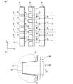
図6は、本発明の第3の実施形態に係る半導体レーザ光学装置の一構成例を概略的に示す図である。図6(a)は、ファスト軸方向から見た平面図であり、図6(b)は、図6(a)における破線の円で囲まれた領域を示す拡大図である。
この第3の実施形態に係る半導体レーザ光学装置は、上記の第1の実施形態に係る半導体レーザ光学装置において、第1のコリメートレンズ20として、反射を利用したスロー軸方向偏向補正機能を有するものが用いられたことの他は、第1の実施形態に係る半導体レーザ光学装置と同一の構成を有する。図6においては、便宜上、第1の実施形態に係る半導体レーザ光学装置と同一の構成部材には、同一の符号が付してある。
図6は、本発明の第3の実施形態に係る半導体レーザ光学装置の一構成例を概略的に示す図である。図6(a)は、ファスト軸方向から見た平面図であり、図6(b)は、図6(a)における破線の円で囲まれた領域を示す拡大図である。
この第3の実施形態に係る半導体レーザ光学装置は、上記の第1の実施形態に係る半導体レーザ光学装置において、第1のコリメートレンズ20として、反射を利用したスロー軸方向偏向補正機能を有するものが用いられたことの他は、第1の実施形態に係る半導体レーザ光学装置と同一の構成を有する。図6においては、便宜上、第1の実施形態に係る半導体レーザ光学装置と同一の構成部材には、同一の符号が付してある。
この例における第1のコリメートレンズ20は、ファスト軸方向から見た平面(X-Z平面)において、平凸シリンドリカルレンズの平坦面における、隣接するエミッタ間の領域に対面する領域の各々に、Z軸方向で第2のコリメートレンズ30側に向かって凸となる台形状の切り欠き部がスロー軸方向に互いに平行に延びるよう形成されている。これにより、隣接する切り欠き部間の領域に、複数の錐台状の偏向補正レンズ部分21が形成されている。各偏向補正レンズ部分21は、エミッタ12の各々に対応してスロー軸方向に一例に並んで配置されている。そして、各々の偏向補正レンズ部分21の平坦面がエミッタ12からのレーザ光が入射される入射面22とされている。各々の偏向補正レンズ部分21の内側面23は、偏向補正レンズ部分21の平坦面より入射されるエミッタ12からのレーザ光のうち、スロー軸方向に比較的大きな発散角度で発散する高角度光成分が臨界反射(全反射)される傾斜角度で形成されている。従って、この第1のコリメートレンズ20は、当該高角度光成分を偏向補正レンズ部分21における内側面23によって全反射させることによりスロー軸方向においてエミッタ12の光軸C側に偏向補正するスロー軸方向偏向補正機能を有するものとして構成されている。
このような構成の半導体レーザ光学装置においても、上記第1の実施形態に係る半導体レーザ光学装置と同様の効果を得ることができる。
<第4の実施形態>
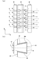
図7は、本発明の第4の実施形態に係る半導体レーザ光学装置の一構成例を概略的に示す図である。図7(a)は、ファスト軸方向から見た平面図であり、図7(b)は、図7(a)における破線の円で囲まれた領域を示す拡大図である。
この第4の実施形態に係る半導体レーザ光学装置は、上記の第1の実施形態に係る半導体レーザ光学装置において、第1のコリメートレンズ20として、反射を利用したスロー軸方向偏向補正機能を有するものが用いられたことの他は、第1の実施形態に係る半導体レーザ光学装置と同一の構成を有する。図7においては、便宜上、第1の実施形態に係る半導体レーザ光学装置と同一の構成部材には、同一の符号が付してある。
図7は、本発明の第4の実施形態に係る半導体レーザ光学装置の一構成例を概略的に示す図である。図7(a)は、ファスト軸方向から見た平面図であり、図7(b)は、図7(a)における破線の円で囲まれた領域を示す拡大図である。
この第4の実施形態に係る半導体レーザ光学装置は、上記の第1の実施形態に係る半導体レーザ光学装置において、第1のコリメートレンズ20として、反射を利用したスロー軸方向偏向補正機能を有するものが用いられたことの他は、第1の実施形態に係る半導体レーザ光学装置と同一の構成を有する。図7においては、便宜上、第1の実施形態に係る半導体レーザ光学装置と同一の構成部材には、同一の符号が付してある。
この例における第1のコリメートレンズ20は、ファスト軸方向から見た平面(X-Z平面)において、平凸シリンドリカルレンズの平坦面における、隣接するエミッタ間の領域に対面する領域の各々に、Z軸方向レーザ光源側に向かって凸となる台形状の凹部28がスロー軸方向に互いに平行に延びるよう形成されている。更に、当該凹部28の傾斜した内側面28Aの表面に反射膜29が形成されており、各々の凹部28における平坦な内端面がエミッタからのレーザ光が入射される入射面22とされている。この第1のコリメートレンズ20においては、凹部28の開口を介して当該凹部28内に入射されるエミッタ12からのレーザ光のうち、スロー軸方向に比較的大きな発散角度で発散する高角度光成分が反射膜29によって反射される。従って、この第1のコリメートレンズ20は、当該高角度光成分をスロー軸方向においてエミッタ12の光軸C側に偏向補正するスロー軸方向偏向補正機能を有するものとして構成されている。
各々の凹部28の内側面28Aの傾斜角度は、入射面22としての凹部28の内端面に入射する光線角度の傾きの符号と、第2のコリメートレンズ30の対応するレンズ要素31の入射面32に入射する光線角度の傾きの符号が一致する角度範囲内で設定されている。
反射膜29は、半導体レーザ素子11から出射されるレーザ光の波長域で高い反射特性(例えば90%以上)を有するものであることが好ましい。このような反射膜29は、例えば、アルミニウムにより構成することができる。反射膜29の厚みは、例えば100~200μmである。
この例における半導体レーザ光学装置においては、第1のコリメートレンズ20における凹部28が形成された平坦面とエミッタ12のレーザ光が出射される端面との光軸方向(Z軸方向)の離間距離は、第1の実施形態に係る半導体レーザ光学装置における当該離間距離よりも小さく設定されている。これは、エミッタ12からのレーザ光を第1のコリメートレンズ20における対応する凹部28内に確実に入射させるためである。
このような構成の半導体レーザ光学装置においても、上記第1の実施形態に係る半導体レーザ光学装置と同様の効果を得ることができる。
以下、本発明の効果を確認するために行った実験例について説明する。
<実験例1>
図1に示す構成に従って、下記に示す仕様を有する本発明に係る半導体レーザ光学装置を作製した。更に、第2のコリメートレンズの出射側に集光レンズを配置すると共に光ファイバ(外径φ0.40mm)をその入射端面が集光レンズの焦点位置に位置されるよう配置し、光ファイバに入射される光束を測定した。その結果、光の利用率は、98.8%であることが確認された。ここに、光の利用率は、光ファイバに入射される光束の大きさを、光ファイバの入射面に照射されていない光成分を含む全光束の大きさで除した値で示される。また、光ファイバの入射端面に形成される照射スポットは、ファスト軸方向の寸法が±0.08mm、スロー軸方向の寸法が±0.2mmであった。この結果より、ファスト軸方向およびスロー軸方向において同等のコリメート性が得られることが確認された。
図1に示す構成に従って、下記に示す仕様を有する本発明に係る半導体レーザ光学装置を作製した。更に、第2のコリメートレンズの出射側に集光レンズを配置すると共に光ファイバ(外径φ0.40mm)をその入射端面が集光レンズの焦点位置に位置されるよう配置し、光ファイバに入射される光束を測定した。その結果、光の利用率は、98.8%であることが確認された。ここに、光の利用率は、光ファイバに入射される光束の大きさを、光ファイバの入射面に照射されていない光成分を含む全光束の大きさで除した値で示される。また、光ファイバの入射端面に形成される照射スポットは、ファスト軸方向の寸法が±0.08mm、スロー軸方向の寸法が±0.2mmであった。この結果より、ファスト軸方向およびスロー軸方向において同等のコリメート性が得られることが確認された。
<半導体レーザ光学装置の仕様>
〔レーザ光源(10)〕
半導体レーザ素子(11)
・外形寸法(X軸方向×Y軸方向×Z軸方向);4mm×0.1mm×1.5mm
・エミッタの数;5個
・一のエミッタにおけるレーザ光出射端面の寸法(X軸方向×Y軸方向);40μm×0.1μm
・隣接するエミッタの中心間距離(配設ピッチ)p;200μm
・レーザ光の発振波長;638nm
・レーザ光のエミッタの光軸に対するファスト軸方向の発散角度;半値全角で±48°
・レーザ光のエミッタの光軸に対するスロー軸方向の発散角度;半値全角で±13°
・出力;8W
〔第1のコリメートレンズ(20)〕
・光軸方向(Z軸方向)の寸法;0.8mm
・屈折率;1.78
・偏向補正レンズ部分における凹状傾斜面の傾斜角度;5°
・入射面における平坦面とエミッタのレーザ光出射端面との光軸方向(Z軸方向)の離間距離;0.16mm
・各々のレンズ部分の凹状傾斜面に入射する光線角度(θ1);10.8°
〔第2のコリメートレンズ(30)〕
・各々のレンズ要素の曲率半径;0.81mm
・屈折率;1.81
・レンズ要素の入射面と第1のコリメートレンズにおける出射面との光軸方向(Z軸方向)の最小離間距離;1.1mm
〔レーザ光源(10)〕
半導体レーザ素子(11)
・外形寸法(X軸方向×Y軸方向×Z軸方向);4mm×0.1mm×1.5mm
・エミッタの数;5個
・一のエミッタにおけるレーザ光出射端面の寸法(X軸方向×Y軸方向);40μm×0.1μm
・隣接するエミッタの中心間距離(配設ピッチ)p;200μm
・レーザ光の発振波長;638nm
・レーザ光のエミッタの光軸に対するファスト軸方向の発散角度;半値全角で±48°
・レーザ光のエミッタの光軸に対するスロー軸方向の発散角度;半値全角で±13°
・出力;8W
〔第1のコリメートレンズ(20)〕
・光軸方向(Z軸方向)の寸法;0.8mm
・屈折率;1.78
・偏向補正レンズ部分における凹状傾斜面の傾斜角度;5°
・入射面における平坦面とエミッタのレーザ光出射端面との光軸方向(Z軸方向)の離間距離;0.16mm
・各々のレンズ部分の凹状傾斜面に入射する光線角度(θ1);10.8°
〔第2のコリメートレンズ(30)〕
・各々のレンズ要素の曲率半径;0.81mm
・屈折率;1.81
・レンズ要素の入射面と第1のコリメートレンズにおける出射面との光軸方向(Z軸方向)の最小離間距離;1.1mm
<比較実験例1>
実験例1において作製した半導体レーザ光学装置において、第1のコリメートレンズとして、広がり抑制機能部分を有さないもの(図4-C参照)を用いたことの他は、実験例1に係る半導体レーザ光学装置と同一の構成を有する比較用の半導体レーザ光学装置を作製した。この比較用の半導体レーザ光学装置について、実験例1と同様の方法により、光の利用率を求めたところ、92%であることが確認された。
実験例1において作製した半導体レーザ光学装置において、第1のコリメートレンズとして、広がり抑制機能部分を有さないもの(図4-C参照)を用いたことの他は、実験例1に係る半導体レーザ光学装置と同一の構成を有する比較用の半導体レーザ光学装置を作製した。この比較用の半導体レーザ光学装置について、実験例1と同様の方法により、光の利用率を求めたところ、92%であることが確認された。
<実験例2>
実験例1において作製した半導体レーザ光学装置において、第1のコリメートレンズとして、図6に示す構成のものを用いたことの他は、実験例1と同一の構成を有する本発明に係る半導体レーザ光学装置を作製した。この第1のコリメートレンズは、下記仕様を有する。この半導体レーザ光学装置について、実験例1と同様の方法により、光の利用率を求めたところ、96%であることが確認された。また、光ファイバの入射端面に形成される照射スポットは、ファスト軸方向の寸法が0.08mm、スロー軸方向の寸法が0.2mmであった。この結果より、ファスト軸方向およびスロー軸方向において同等のコリメート性が得られることが確認された。
実験例1において作製した半導体レーザ光学装置において、第1のコリメートレンズとして、図6に示す構成のものを用いたことの他は、実験例1と同一の構成を有する本発明に係る半導体レーザ光学装置を作製した。この第1のコリメートレンズは、下記仕様を有する。この半導体レーザ光学装置について、実験例1と同様の方法により、光の利用率を求めたところ、96%であることが確認された。また、光ファイバの入射端面に形成される照射スポットは、ファスト軸方向の寸法が0.08mm、スロー軸方向の寸法が0.2mmであった。この結果より、ファスト軸方向およびスロー軸方向において同等のコリメート性が得られることが確認された。
〔第1のコリメートレンズの仕様〕
・光軸方向(Z軸方向)の寸法;0.8mm
・屈折率;1.78
・偏向補正レンズ部分における内側面の傾斜角度;0.5°
・偏向補正レンズ部分の入射面とエミッタのレーザ光出射端面との光軸方向(Z軸方向)の離間距離;0.15mm
・偏向補正レンズ部分の入射面に入射する光線角度;10°
・光軸方向(Z軸方向)の寸法;0.8mm
・屈折率;1.78
・偏向補正レンズ部分における内側面の傾斜角度;0.5°
・偏向補正レンズ部分の入射面とエミッタのレーザ光出射端面との光軸方向(Z軸方向)の離間距離;0.15mm
・偏向補正レンズ部分の入射面に入射する光線角度;10°
<実験例3>
実験例1において作製した半導体レーザ光学装置において、第1のコリメートレンズとして、図7に示す構成のものを用いたことの他は、実験例1と同一の構成を有する本発明に係る半導体レーザ光学装置を作製した。この第1のコリメートレンズは、下記仕様を有する。この半導体レーザ光学装置について、実験例1と同様の方法により、光の利用率を求めたところ、95%であることが確認された。また、光ファイバの入射端面に形成される照射スポットは、ファスト軸方向の寸法が0.08mm、スロー軸方向の寸法が0.2mmであった。この結果より、ファスト軸方向およびスロー軸方向において同等のコリメート性が得られることが確認された。
実験例1において作製した半導体レーザ光学装置において、第1のコリメートレンズとして、図7に示す構成のものを用いたことの他は、実験例1と同一の構成を有する本発明に係る半導体レーザ光学装置を作製した。この第1のコリメートレンズは、下記仕様を有する。この半導体レーザ光学装置について、実験例1と同様の方法により、光の利用率を求めたところ、95%であることが確認された。また、光ファイバの入射端面に形成される照射スポットは、ファスト軸方向の寸法が0.08mm、スロー軸方向の寸法が0.2mmであった。この結果より、ファスト軸方向およびスロー軸方向において同等のコリメート性が得られることが確認された。
〔第1のコリメートレンズの仕様〕
・光軸方向(Z軸方向)の寸法;0.8mm
・屈折率;1.78
・凹部の開口におけるスロー軸方向の寸法;0.5mm
・凹部の内側面の傾斜角度;0.5°
・平坦面とエミッタのレーザ光出射端面との光軸方向(Z軸方向)の離間距離;0.16mm
・凹部における入射面に入射する光線角度;10°
・反射膜の材質;アルミニウム
・反射膜のレーザ光の波長に対する反射率;90%
・反射膜の厚み;100μm
・光軸方向(Z軸方向)の寸法;0.8mm
・屈折率;1.78
・凹部の開口におけるスロー軸方向の寸法;0.5mm
・凹部の内側面の傾斜角度;0.5°
・平坦面とエミッタのレーザ光出射端面との光軸方向(Z軸方向)の離間距離;0.16mm
・凹部における入射面に入射する光線角度;10°
・反射膜の材質;アルミニウム
・反射膜のレーザ光の波長に対する反射率;90%
・反射膜の厚み;100μm
以上のように、本発明に係る半導体レーザ光学装置によれば、比較用の半導体レーザ光学装置に比して高い光の利用率が得られ、従って、高いコリメート効率を得ることができることが確認された。
以上、本発明の実施形態について説明したが、本発明は上記の実施形態に限定されるものではなく、種々の変更を加えることができる。
例えば、第1の実施形態に係る半導体レーザ光学装置における広がり抑制機能部分および第2の実施形態に係る半導体レーザ光学装置における第1の広がり抑制機能部分は、凸状傾斜面により構成されていてもよい。また、第2の実施形態に係る半導体レーザ光学装置における第2の広がり抑制機能部分が凹状傾斜面により構成されていてもよい。
また、レーザ光源としては、複数のエミッタがスロー軸方向に一列に並んで配置されてなるアレイ型のものに限定されない。また、複数のエミッタがスロー軸方向に一列に並んで配置されてなる例えばチップ状の半導体レーザ素子の複数のものがファスト軸方向に積重された構成のものであってもよい。
例えば、第1の実施形態に係る半導体レーザ光学装置における広がり抑制機能部分および第2の実施形態に係る半導体レーザ光学装置における第1の広がり抑制機能部分は、凸状傾斜面により構成されていてもよい。また、第2の実施形態に係る半導体レーザ光学装置における第2の広がり抑制機能部分が凹状傾斜面により構成されていてもよい。
また、レーザ光源としては、複数のエミッタがスロー軸方向に一列に並んで配置されてなるアレイ型のものに限定されない。また、複数のエミッタがスロー軸方向に一列に並んで配置されてなる例えばチップ状の半導体レーザ素子の複数のものがファスト軸方向に積重された構成のものであってもよい。
10 レーザ光源
11 半導体レーザ素子
12 エミッタ
20 第1のコリメートレンズ
21 偏向補正レンズ部分
21A 入射側偏向補正レンズ部分
22 入射面
22A 凹状傾斜面
23 内側面
25 広がり抑制機能部分
25A 第1の広がり抑制機能部分
25B 第2の広がり抑制機能部分
26 出射側偏向補正レンズ部分
27 出射面
27A 凸状傾斜面
28 凹部
28A 内側面
29 反射膜
30 第2のコリメートレンズ
31 レンズ要素
32 入射面
35 出射面
40 ファスト軸方向コリメートレンズ
50 スロー軸方向コリメートレンズ
51,51a,51b,51c レンズ要素
C エミッタの光軸
11 半導体レーザ素子
12 エミッタ
20 第1のコリメートレンズ
21 偏向補正レンズ部分
21A 入射側偏向補正レンズ部分
22 入射面
22A 凹状傾斜面
23 内側面
25 広がり抑制機能部分
25A 第1の広がり抑制機能部分
25B 第2の広がり抑制機能部分
26 出射側偏向補正レンズ部分
27 出射面
27A 凸状傾斜面
28 凹部
28A 内側面
29 反射膜
30 第2のコリメートレンズ
31 レンズ要素
32 入射面
35 出射面
40 ファスト軸方向コリメートレンズ
50 スロー軸方向コリメートレンズ
51,51a,51b,51c レンズ要素
C エミッタの光軸
Claims (3)
- 半導体レーザ素子を備えたレーザ光源と、
当該レーザ光源のレーザ光出射側に設けられた、当該レーザ光源から出射されるレーザ光のファスト軸方向に発散する光成分をコリメートする第1のコリメートレンズと、
当該第1のコリメートレンズの出射側に設けられた、当該第1のコリメートレンズから出射された光のスロー軸方向に発散する光成分をコリメートする第2のコリメートレンズと
を具備した半導体レーザ光学装置において、
前記第1のコリメートレンズは、スロー軸方向に対する広がりが抑制された光を前記第2のコリメートレンズに入射させる機能を有することを特徴とする半導体レーザ光学装置。 - 前記第1のコリメートレンズは、入射面および出射面のいずれか一方または両方におけるスロー軸方向の側縁領域に広がり抑制機能部分を有することを特徴とする請求項1に記載の半導体レーザ光学装置。
- 前記レーザ光源を構成する半導体レーザ素子は、複数のエミッタが一列に並んで配置されていることを特徴とする請求項1または請求項2に記載の半導体レーザ光学装置。
Priority Applications (2)
| Application Number | Priority Date | Filing Date | Title |
|---|---|---|---|
| US14/388,813 US20150049779A1 (en) | 2012-04-03 | 2013-03-12 | Semiconductor laser optical device |
| CN201380018603.8A CN104205530A (zh) | 2012-04-03 | 2013-03-12 | 半导体激光光学装置 |
Applications Claiming Priority (2)
| Application Number | Priority Date | Filing Date | Title |
|---|---|---|---|
| JP2012-084830 | 2012-04-03 | ||
| JP2012084830A JP2013214651A (ja) | 2012-04-03 | 2012-04-03 | 半導体レーザ光学装置 |
Publications (1)
| Publication Number | Publication Date |
|---|---|
| WO2013150864A1 true WO2013150864A1 (ja) | 2013-10-10 |
Family
ID=49300361
Family Applications (1)
| Application Number | Title | Priority Date | Filing Date |
|---|---|---|---|
| PCT/JP2013/056722 Ceased WO2013150864A1 (ja) | 2012-04-03 | 2013-03-12 | 半導体レーザ光学装置 |
Country Status (4)
| Country | Link |
|---|---|
| US (1) | US20150049779A1 (ja) |
| JP (1) | JP2013214651A (ja) |
| CN (1) | CN104205530A (ja) |
| WO (1) | WO2013150864A1 (ja) |
Families Citing this family (13)
| Publication number | Priority date | Publication date | Assignee | Title |
|---|---|---|---|---|
| CN107045165A (zh) * | 2016-02-05 | 2017-08-15 | 苏州旭创科技有限公司 | 光学组件及光模块 |
| EP3355097A1 (de) * | 2017-01-31 | 2018-08-01 | Fisba AG | Vorrichtung zur kollimation eines lichtstrahls, hochleistungslaser und fokussieroptik sowie verfahren zum kollimieren eines lichtstrahles |
| CN107453201A (zh) * | 2017-09-08 | 2017-12-08 | 深圳市三千米光电科技有限公司 | 能进行vcsel激光器发散角压缩的装置 |
| US20200191957A1 (en) * | 2018-12-18 | 2020-06-18 | Didi Research America, Llc | Transmitter having beam-shaping component for light detection and ranging (lidar) |
| CN110133623B (zh) * | 2019-05-05 | 2021-05-14 | 深圳市速腾聚创科技有限公司 | 激光发射装置、激光雷达及智能装置 |
| CN112585490B (zh) * | 2019-07-29 | 2023-08-04 | 深圳市速腾聚创科技有限公司 | 激光发射模组及其装调方法、激光雷达及智能感应设备 |
| CN110707529A (zh) * | 2019-10-29 | 2020-01-17 | 深圳市柠檬光子科技有限公司 | 半导体激光器、半导体激光模块以及激光设备 |
| WO2021083641A1 (en) * | 2019-10-30 | 2021-05-06 | Trumpf Photonic Components Gmbh | Light source, sensor and method of illuminating a scene |
| EP4067978B1 (en) * | 2019-11-28 | 2025-04-16 | Panasonic Holdings Corporation | Beam coupling device, and laser processing machine |
| CN114846703B (zh) * | 2019-12-06 | 2025-08-12 | 古河电气工业株式会社 | 发光装置、光源单元、光源装置及光纤激光器 |
| CN113064136A (zh) | 2020-01-02 | 2021-07-02 | 隆达电子股份有限公司 | 发光元件与发光模块 |
| JP6816322B1 (ja) * | 2020-04-28 | 2021-01-20 | デクセリアルズ株式会社 | レーザー装置、投射型画像表示装置及びセンシング装置 |
| CN113655487B (zh) * | 2021-09-16 | 2024-08-13 | 中国电子科技集团公司第四十四研究所 | 一种连续视场激光近程探测前端装置 |
Citations (9)
| Publication number | Priority date | Publication date | Assignee | Title |
|---|---|---|---|---|
| JPH0743643A (ja) * | 1993-07-28 | 1995-02-14 | Nippon Steel Corp | 半導体レーザ集光器 |
| JPH0996760A (ja) * | 1995-09-29 | 1997-04-08 | Mitsui Petrochem Ind Ltd | 光学装置 |
| JPH10335755A (ja) * | 1997-06-05 | 1998-12-18 | Sony Corp | 半導体レーザ装置 |
| JP2002239773A (ja) * | 2000-12-11 | 2002-08-28 | Matsushita Electric Ind Co Ltd | 半導体レーザー加工装置および半導体レーザー加工方法 |
| JP2002286914A (ja) * | 2000-11-27 | 2002-10-03 | Mas Fab Wifag | イメージ作成装置 |
| WO2002077698A1 (en) * | 2001-03-26 | 2002-10-03 | Hamamatsu Photonics K.K. | Semiconductor laser device |
| JP2003103389A (ja) * | 2001-09-27 | 2003-04-08 | Toyoda Mach Works Ltd | 半導体レーザ集光装置 |
| JP2007298886A (ja) * | 2006-05-02 | 2007-11-15 | Hitachi Cable Ltd | レンズ部品及び光モジュール |
| JP2009520353A (ja) * | 2005-12-15 | 2009-05-21 | マインド メルターズ, インコーポレーテッド | レーザダイオードアレーから強力レーザ光を発生するシステムおよび方法 |
Family Cites Families (1)
| Publication number | Priority date | Publication date | Assignee | Title |
|---|---|---|---|---|
| DE19819333A1 (de) * | 1998-04-30 | 1999-11-04 | Lissotschenko Vitaly | Optisches Emitter-Array mit Kollimationsoptik |
-
2012
- 2012-04-03 JP JP2012084830A patent/JP2013214651A/ja active Pending
-
2013
- 2013-03-12 CN CN201380018603.8A patent/CN104205530A/zh active Pending
- 2013-03-12 US US14/388,813 patent/US20150049779A1/en not_active Abandoned
- 2013-03-12 WO PCT/JP2013/056722 patent/WO2013150864A1/ja not_active Ceased
Patent Citations (9)
| Publication number | Priority date | Publication date | Assignee | Title |
|---|---|---|---|---|
| JPH0743643A (ja) * | 1993-07-28 | 1995-02-14 | Nippon Steel Corp | 半導体レーザ集光器 |
| JPH0996760A (ja) * | 1995-09-29 | 1997-04-08 | Mitsui Petrochem Ind Ltd | 光学装置 |
| JPH10335755A (ja) * | 1997-06-05 | 1998-12-18 | Sony Corp | 半導体レーザ装置 |
| JP2002286914A (ja) * | 2000-11-27 | 2002-10-03 | Mas Fab Wifag | イメージ作成装置 |
| JP2002239773A (ja) * | 2000-12-11 | 2002-08-28 | Matsushita Electric Ind Co Ltd | 半導体レーザー加工装置および半導体レーザー加工方法 |
| WO2002077698A1 (en) * | 2001-03-26 | 2002-10-03 | Hamamatsu Photonics K.K. | Semiconductor laser device |
| JP2003103389A (ja) * | 2001-09-27 | 2003-04-08 | Toyoda Mach Works Ltd | 半導体レーザ集光装置 |
| JP2009520353A (ja) * | 2005-12-15 | 2009-05-21 | マインド メルターズ, インコーポレーテッド | レーザダイオードアレーから強力レーザ光を発生するシステムおよび方法 |
| JP2007298886A (ja) * | 2006-05-02 | 2007-11-15 | Hitachi Cable Ltd | レンズ部品及び光モジュール |
Also Published As
| Publication number | Publication date |
|---|---|
| US20150049779A1 (en) | 2015-02-19 |
| CN104205530A (zh) | 2014-12-10 |
| JP2013214651A (ja) | 2013-10-17 |
Similar Documents
| Publication | Publication Date | Title |
|---|---|---|
| WO2013150864A1 (ja) | 半導体レーザ光学装置 | |
| US7668214B2 (en) | Light source | |
| US9594252B2 (en) | LD module | |
| US11108214B2 (en) | Wavelength combining laser apparatus | |
| EP2908517B1 (en) | Laser beam-combining optical device | |
| JP2020061591A (ja) | レーザモジュール | |
| EP3687008A1 (en) | Light source unit | |
| CN112673294B (zh) | 复用光学系统 | |
| US20190162973A1 (en) | Light source device | |
| JP7165337B2 (ja) | 光結合装置 | |
| WO2018142657A1 (ja) | 導光装置、レーザモジュール、及び導光装置の製造方法 | |
| TWI515465B (zh) | 光耦合元件及應用光耦合元件之光學模組 | |
| JP2020009843A (ja) | 光源装置、プロジェクタ | |
| US20140049830A1 (en) | Arrangement For Shaping Laser Radiation | |
| JP7600530B2 (ja) | 光源装置、プロジェクタおよび機械加工装置 | |
| WO2018037548A1 (ja) | 発光装置 | |
| JP6635725B2 (ja) | 投影装置 | |
| JP7331902B2 (ja) | 光源装置及び投影装置 | |
| KR102529166B1 (ko) | 레이저 모듈 패키지 | |
| JP7151497B2 (ja) | 光源装置 | |
| JP4774797B2 (ja) | 光路変換装置およびレーザモジュール | |
| US11187915B2 (en) | Parallel light generation device | |
| JP3952894B2 (ja) | レーザ発光装置 | |
| JP2005191094A (ja) | 半導体レーザ装置 | |
| TW202234105A (zh) | 雷射二極體三維耦光方法及其雷射系統 |
Legal Events
| Date | Code | Title | Description |
|---|---|---|---|
| 121 | Ep: the epo has been informed by wipo that ep was designated in this application |
Ref document number: 13772998 Country of ref document: EP Kind code of ref document: A1 |
|
| WWE | Wipo information: entry into national phase |
Ref document number: 14388813 Country of ref document: US |
|
| NENP | Non-entry into the national phase |
Ref country code: DE |
|
| 122 | Ep: pct application non-entry in european phase |
Ref document number: 13772998 Country of ref document: EP Kind code of ref document: A1 |