WO2013145894A1 - ケーブル接続構造、超音波探触子および超音波内視鏡システム - Google Patents
ケーブル接続構造、超音波探触子および超音波内視鏡システム Download PDFInfo
- Publication number
- WO2013145894A1 WO2013145894A1 PCT/JP2013/053118 JP2013053118W WO2013145894A1 WO 2013145894 A1 WO2013145894 A1 WO 2013145894A1 JP 2013053118 W JP2013053118 W JP 2013053118W WO 2013145894 A1 WO2013145894 A1 WO 2013145894A1
- Authority
- WO
- WIPO (PCT)
- Prior art keywords
- cable
- substrate
- connection structure
- cable connection
- electrode
- Prior art date
- Legal status (The legal status is an assumption and is not a legal conclusion. Google has not performed a legal analysis and makes no representation as to the accuracy of the status listed.)
- Ceased
Links
Images









Classifications
-
- G—PHYSICS
- G01—MEASURING; TESTING
- G01N—INVESTIGATING OR ANALYSING MATERIALS BY DETERMINING THEIR CHEMICAL OR PHYSICAL PROPERTIES
- G01N29/00—Investigating or analysing materials by the use of ultrasonic, sonic or infrasonic waves; Visualisation of the interior of objects by transmitting ultrasonic or sonic waves through the object
- G01N29/22—Details, e.g. general constructional or apparatus details
- G01N29/24—Probes
-
- H—ELECTRICITY
- H01—ELECTRIC ELEMENTS
- H01R—ELECTRICALLY-CONDUCTIVE CONNECTIONS; STRUCTURAL ASSOCIATIONS OF A PLURALITY OF MUTUALLY-INSULATED ELECTRICAL CONNECTING ELEMENTS; COUPLING DEVICES; CURRENT COLLECTORS
- H01R13/00—Details of coupling devices of the kinds covered by groups H01R12/70 or H01R24/00 - H01R33/00
- H01R13/44—Means for preventing access to live contacts
- H01R13/447—Shutter or cover plate
-
- A—HUMAN NECESSITIES
- A61—MEDICAL OR VETERINARY SCIENCE; HYGIENE
- A61B—DIAGNOSIS; SURGERY; IDENTIFICATION
- A61B8/00—Diagnosis using ultrasonic, sonic or infrasonic waves
- A61B8/12—Diagnosis using ultrasonic, sonic or infrasonic waves in body cavities or body tracts, e.g. by using catheters
-
- A—HUMAN NECESSITIES
- A61—MEDICAL OR VETERINARY SCIENCE; HYGIENE
- A61B—DIAGNOSIS; SURGERY; IDENTIFICATION
- A61B8/00—Diagnosis using ultrasonic, sonic or infrasonic waves
- A61B8/44—Constructional features of the ultrasonic, sonic or infrasonic diagnostic device
- A61B8/4444—Constructional features of the ultrasonic, sonic or infrasonic diagnostic device related to the probe
- A61B8/445—Details of catheter construction
-
- A—HUMAN NECESSITIES
- A61—MEDICAL OR VETERINARY SCIENCE; HYGIENE
- A61B—DIAGNOSIS; SURGERY; IDENTIFICATION
- A61B8/00—Diagnosis using ultrasonic, sonic or infrasonic waves
- A61B8/44—Constructional features of the ultrasonic, sonic or infrasonic diagnostic device
- A61B8/4483—Constructional features of the ultrasonic, sonic or infrasonic diagnostic device characterised by features of the ultrasound transducer
- A61B8/4494—Constructional features of the ultrasonic, sonic or infrasonic diagnostic device characterised by features of the ultrasound transducer characterised by the arrangement of the transducer elements
-
- G—PHYSICS
- G01—MEASURING; TESTING
- G01N—INVESTIGATING OR ANALYSING MATERIALS BY DETERMINING THEIR CHEMICAL OR PHYSICAL PROPERTIES
- G01N29/00—Investigating or analysing materials by the use of ultrasonic, sonic or infrasonic waves; Visualisation of the interior of objects by transmitting ultrasonic or sonic waves through the object
- G01N29/22—Details, e.g. general constructional or apparatus details
- G01N29/32—Arrangements for suppressing undesired influences, e.g. temperature or pressure variations, compensating for signal noise
-
- H—ELECTRICITY
- H01—ELECTRIC ELEMENTS
- H01R—ELECTRICALLY-CONDUCTIVE CONNECTIONS; STRUCTURAL ASSOCIATIONS OF A PLURALITY OF MUTUALLY-INSULATED ELECTRICAL CONNECTING ELEMENTS; COUPLING DEVICES; CURRENT COLLECTORS
- H01R12/00—Structural associations of a plurality of mutually-insulated electrical connecting elements, specially adapted for printed circuits, e.g. printed circuit boards [PCB], flat or ribbon cables, or like generally planar structures, e.g. terminal strips, terminal blocks; Coupling devices specially adapted for printed circuits, flat or ribbon cables, or like generally planar structures; Terminals specially adapted for contact with, or insertion into, printed circuits, flat or ribbon cables, or like generally planar structures
- H01R12/50—Fixed connections
- H01R12/59—Fixed connections for flexible printed circuits, flat or ribbon cables or like structures
- H01R12/594—Fixed connections for flexible printed circuits, flat or ribbon cables or like structures for shielded flat cable
- H01R12/598—Each conductor being individually surrounded by shield, e.g. multiple coaxial cables in flat structure
-
- H—ELECTRICITY
- H01—ELECTRIC ELEMENTS
- H01R—ELECTRICALLY-CONDUCTIVE CONNECTIONS; STRUCTURAL ASSOCIATIONS OF A PLURALITY OF MUTUALLY-INSULATED ELECTRICAL CONNECTING ELEMENTS; COUPLING DEVICES; CURRENT COLLECTORS
- H01R13/00—Details of coupling devices of the kinds covered by groups H01R12/70 or H01R24/00 - H01R33/00
- H01R13/648—Protective earth or shield arrangements on coupling devices, e.g. anti-static shielding
- H01R13/655—Protective earth or shield arrangements on coupling devices, e.g. anti-static shielding with earth brace
-
- H—ELECTRICITY
- H01—ELECTRIC ELEMENTS
- H01R—ELECTRICALLY-CONDUCTIVE CONNECTIONS; STRUCTURAL ASSOCIATIONS OF A PLURALITY OF MUTUALLY-INSULATED ELECTRICAL CONNECTING ELEMENTS; COUPLING DEVICES; CURRENT COLLECTORS
- H01R35/00—Flexible or turnable line connectors, i.e. the rotation angle being limited
- H01R35/02—Flexible line connectors without frictional contact members
-
- H—ELECTRICITY
- H05—ELECTRIC TECHNIQUES NOT OTHERWISE PROVIDED FOR
- H05K—PRINTED CIRCUITS; CASINGS OR CONSTRUCTIONAL DETAILS OF ELECTRIC APPARATUS; MANUFACTURE OF ASSEMBLAGES OF ELECTRICAL COMPONENTS
- H05K1/00—Printed circuits
- H05K1/02—Details
- H05K1/0213—Electrical arrangements not otherwise provided for
- H05K1/0215—Grounding of printed circuits by connection to external grounding means
-
- H—ELECTRICITY
- H05—ELECTRIC TECHNIQUES NOT OTHERWISE PROVIDED FOR
- H05K—PRINTED CIRCUITS; CASINGS OR CONSTRUCTIONAL DETAILS OF ELECTRIC APPARATUS; MANUFACTURE OF ASSEMBLAGES OF ELECTRICAL COMPONENTS
- H05K1/00—Printed circuits
- H05K1/02—Details
- H05K1/11—Printed elements for providing electric connections to or between printed circuits
- H05K1/111—Pads for surface mounting, e.g. lay-out
-
- A—HUMAN NECESSITIES
- A61—MEDICAL OR VETERINARY SCIENCE; HYGIENE
- A61B—DIAGNOSIS; SURGERY; IDENTIFICATION
- A61B1/00—Instruments for performing medical examinations of the interior of cavities or tubes of the body by visual or photographical inspection, e.g. endoscopes; Illuminating arrangements therefor
- A61B1/00112—Connection or coupling means
- A61B1/00114—Electrical cables in or with an endoscope
-
- A—HUMAN NECESSITIES
- A61—MEDICAL OR VETERINARY SCIENCE; HYGIENE
- A61B—DIAGNOSIS; SURGERY; IDENTIFICATION
- A61B1/00—Instruments for performing medical examinations of the interior of cavities or tubes of the body by visual or photographical inspection, e.g. endoscopes; Illuminating arrangements therefor
- A61B1/00112—Connection or coupling means
- A61B1/00121—Connectors, fasteners and adapters, e.g. on the endoscope handle
- A61B1/00124—Connectors, fasteners and adapters, e.g. on the endoscope handle electrical, e.g. electrical plug-and-socket connection
-
- G—PHYSICS
- G01—MEASURING; TESTING
- G01N—INVESTIGATING OR ANALYSING MATERIALS BY DETERMINING THEIR CHEMICAL OR PHYSICAL PROPERTIES
- G01N2291/00—Indexing codes associated with group G01N29/00
- G01N2291/26—Scanned objects
- G01N2291/263—Surfaces
- G01N2291/2636—Surfaces cylindrical from inside
-
- H—ELECTRICITY
- H01—ELECTRIC ELEMENTS
- H01R—ELECTRICALLY-CONDUCTIVE CONNECTIONS; STRUCTURAL ASSOCIATIONS OF A PLURALITY OF MUTUALLY-INSULATED ELECTRICAL CONNECTING ELEMENTS; COUPLING DEVICES; CURRENT COLLECTORS
- H01R12/00—Structural associations of a plurality of mutually-insulated electrical connecting elements, specially adapted for printed circuits, e.g. printed circuit boards [PCB], flat or ribbon cables, or like generally planar structures, e.g. terminal strips, terminal blocks; Coupling devices specially adapted for printed circuits, flat or ribbon cables, or like generally planar structures; Terminals specially adapted for contact with, or insertion into, printed circuits, flat or ribbon cables, or like generally planar structures
- H01R12/50—Fixed connections
- H01R12/59—Fixed connections for flexible printed circuits, flat or ribbon cables or like structures
- H01R12/61—Fixed connections for flexible printed circuits, flat or ribbon cables or like structures connecting to flexible printed circuits, flat or ribbon cables or like structures
Definitions
- the present invention relates to a cable connection structure for connecting a cable and a substrate, an ultrasonic probe to which the cable connection structure is applied, and an ultrasonic endoscope system.
- an FPC as a substrate on which a semiconductor component is mounted has an extension portion, and the extension portion can be bent to cover light and shield the light by shielding the semiconductor component (for example, patent document 2).
- Patent Document 2 since the semiconductor component is integrally covered by the extending portion, incident noise from the outside is further simplified in comparison with Patent Document 1 in which shielding is performed using a separate member. , And radiation noise from the inside can be shielded.
- Patent Document 1 considers the crosstalk between the cables when a plurality of cables (terminals) are accommodated in the FPC while the number of manufacturing steps such as solder processing for fixing the FPC increases. It was not possible to suppress the signal interference between the cables.
- Patent Document 2 is not a configuration in which the extending part is provided for the semiconductor component and is shielded against the cable connected to the substrate, and therefore, the crosstalk between the cables as described above It was not possible to suppress the signal interference between the cables.
- the present invention has been made in view of the above, and has a cable connection structure, an ultrasonic probe and an ultrasonic endoscope which can easily constitute a shield structure and can suppress interference of signals between cables. It aims to provide a system.
- a cable connection structure is a cable connection structure for connecting a plurality of cables and electrodes provided on a substrate, wherein the cable or the substrate is And an extension portion that extends from the cable or the substrate and covers at least a connection portion between the cable and the electrode.
- the cable connection structure according to the present invention is characterized in that, in the above invention, the cable connection structure further includes a ground electrode which covers at least a part of the substrate and the extension and which is electrically grounded.
- the cable connection structure according to the present invention is characterized in that, in the above invention, the cable fixing structure further includes an insulating fixing member disposed between the substrate and the extension portion.
- the substrate and the extension portion are made of a bendable insulating film, the extension portion is provided on the substrate, and the arrangement of the electrodes is It is characterized in that it extends along the direction.
- the cable is a lead terminal, and the plurality of lead terminals respectively project from one end of a base material made of a bendable insulating film,
- the recessed portion is made of a bendable insulating film, provided on the base and extending along the arrangement direction of the lead terminals.
- the cable is a lead terminal, and the plurality of lead terminals respectively project from one end of a base material made of a bendable insulating film,
- the recessed portion is made of a bendable insulating film, and is provided on the substrate and extends along a direction perpendicular to the arrangement direction of the lead terminals.
- the ultrasonic probe according to the present invention is integrally provided with a plurality of cables, a substrate provided with electrodes, a transducer module mounted on the substrate, the cable or the substrate, And a cable or an extension extending from the substrate and covering at least a connection portion between the cable and the electrode.
- the ultrasound endoscope system further includes an insertion unit which is inserted into the body of the subject and outputs an ultrasound signal in the body, and acquires the ultrasound signal reflected in the body. It is an ultrasonic endoscope system, and the ultrasonic probe concerning the above-mentioned invention was provided in the tip of the above-mentioned insertion part.
- the shield structure is simply configured.
- the present invention has the effect of being able to suppress signal interference between cables.
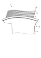
- FIG. 1 is a schematic view showing a cable connection structure according to a first embodiment of the present invention.
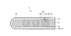
- FIG. 2 is a partial cross-sectional view of the electronic device taken along line AA of FIG.
- FIG. 3 is a schematic view showing a cable connection structure according to the first embodiment of the present invention.
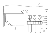
- FIG. 4 is a schematic view showing a cable connection structure according to a modified example 1-1 of the first embodiment of the present invention.
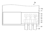
- FIG. 5 is a schematic view showing a cable connection structure according to Modification 1-1 of Embodiment 1 of the present invention.
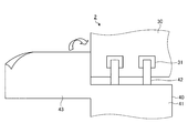
- FIG. 8 is a schematic view showing a cable connection structure according to Embodiment 2 of the present invention.
- FIG. 9 is a schematic view showing a cable connection structure according to a modified example 2-1 of the second embodiment of the present invention.
- FIG. 10 is a schematic view showing a cable connection structure according to a modified example 2-1 of the second embodiment of the present invention.
- FIG. 11 is a cross-sectional view taken along the line CC of the cable connection structure shown in FIG.
- FIG. 12 is a perspective view schematically showing a cable connection structure which is a modified example 2-2 of the second embodiment of the present invention.
- FIG. 13 is a schematic view showing the configuration of a substrate of the cable connection structure shown in FIG. FIG.
- FIG. 14 is an exploded perspective view schematically showing a cable connection structure which is a modified example 2-2 of the second embodiment of the present invention.
- FIG. 15 is a perspective view schematically showing a cable connection structure which is a modified example 2-2 of the second embodiment of the present invention.
- FIG. 16 is a schematic view showing a configuration of a transducer module connected to the cable connection structure according to the third embodiment of the present invention.
- FIG. 17 is a schematic view showing the configuration of the board of the cable connection structure according to the third embodiment of the present invention.
- FIG. 18 is a perspective view schematically showing an ultrasonic probe including the cable connection structure according to the third embodiment of the present invention.
- FIG. 19 is a perspective view schematically showing an ultrasonic probe including the cable connection structure according to the third embodiment of the present invention.
- FIG. 20 is a schematic view showing an ultrasonic endoscope system using an ultrasonic probe including the cable connection structure according to the third embodiment of the present invention.
- FIG. 1 is a schematic view showing a cable connection structure according to a first embodiment.
- FIG. 2 is a partial cross-sectional view of the electronic device taken along line AA of FIG.
- FIG. 3 is a schematic view showing a cable connection structure according to the first embodiment.
- the cable connection structure 1 according to the first embodiment includes a substrate 10 and a plurality of cables 20 connected to the substrate 10.
- the cable 20 will be described as being a coaxial cable.
- the substrate 10 is an FPC made of a bendable insulating film, and has a substantially rectangular circuit forming portion 11 on which an electric circuit, an electrode and the like are formed, and an electrode 12 electrically connected to the cable 20 on one surface. , 13 and. Further, the substrate 10 is made of a bendable insulating film, provided on the surface on the side different from the connection side with the extension portion 14 extending from the end portion of the circuit forming portion 11 and the cable 20, and made of copper or the like. A ground electrode 15 is provided.
- the electrode 12 is a core wire connection electrode connected to the core wire 21 of the cable 20 described later
- the electrode 13 is a shield wire connection electrode connected to the shield wire 23.
- the substrate 10 is electrically grounded via the ground electrode 15.
- the ground electrode 15 may be provided inside the insulating film as long as the ground electrode 15 is located at the outermost side on the surface different from the connection side with the cable 20.
- the cable 20 includes a core 21 formed of a conductor made of copper or the like, an insulator, and covers the outer periphery of the core 21 and also has an inner insulating layer 22 that exposes the core 21 at the tip end, and the inner insulating layer 22.
- a shield wire 23 made of a conductor that covers the outer periphery, and an outer insulating layer 24 made of an insulator that covers the outer periphery of the shield wire 23 are provided.
- the cable 20 has a step in which the inner insulating layer 22, the shield wire 23 and the outer insulating layer 24 are stepped at the end connected to the substrate 10.
- the electrode 12 and the core wire 21 are electrically connected by, for example, a conductive bonding material such as solder. Also in the electrode 13 and the shield wire 23, the electrode 13 and the shield wire 23 are electrically connected by a conductive bonding material such as solder, for example.
- the plurality of cables 20 are arranged in accordance with the arrangement of the respective electrodes 12.
- the extending portions 14 extend in this arrangement direction (see FIG. 3).
- the distance d1 in the arrangement direction from the base end of the extension portion 14 is the distance to at least the end of the member farthest from the base end of the electrodes 12, 13 or the cable 20 (in the first embodiment, the electrode It is provided so as to be equal to or more than the distance d2) to the end of 13.
- the distance in the direction orthogonal to the arrangement direction is the distance of the end of the electrode 12 or the core wire 21 beyond the end farthest from the proximal end in the direction orthogonal to the arrangement direction. It is preferable that the distance be determined in consideration of the thickness of the cable 20 and the electrodes 12 and 13.
- the extension 14 is bent from the proximal end in the arrangement direction to cover the electrodes 12 and 13 and the cable 20.
- damage to the electrodes 12 and 13 and the cable 20 can be prevented with a simple configuration, and incident noise from the outside and radiation noise from the inside can be shielded.
- the ground electrode is provided on the outer surface side in the region covered by the extension portion 14, necessary insulation can be ensured even when the cable connection structure 1 is damaged.
- an adhesive material G (fixing member) made of an insulating resin is filled between the circuit forming portion 11, the extension portion 14 and the cable 20, and the positional relationship between them is determined. It is fixed.
- the adhesive G is filled between the circuit forming portion 11, the extension portion 14 and the cable 20, the positional relationship between them is fixed, so that the signal line of each cable 20 and the outer surface of the extension portion 14 Since the distance between the ground electrode 15 and the ground electrode 15 can be properly maintained, interference between signals transmitted by the cables 20 can be suppressed.
- the extension 12 covering the electrodes 12 and 13 and the cable 20 is provided, and the space formed by the extension 14 is bonded. Since the filling with the agent G is performed, incident noise from the outside and radiation noise from the inside can be shielded with a simple configuration, and signal interference between cables can be suppressed.
- the space formed by the circuit forming portion 11, the extending portion 14 and the cable 20 is described as being filled with the adhesive G.
- the adhesive G may be partially provided as long as the positional relationship of the cables 20 can be fixed and the cables 20 can be disposed so as to cover them.
- the adhesive G is extended to the circuit forming portion 11 and It may be fixed only between the existing part 14 and the other part.
- the adhesive agent G is applicable if it is resin etc. which have the insulation which can fix the positional relationship of the circuit formation part 11, the extension part 14, and the cable 20.
- the ground electrode 15 is described as covering the entire outer peripheral side of the circuit forming portion 11 and the extending portion 14, but if grounding is possible, the circuit forming portion 11 and the extending portion 14 A part of the outer peripheral side may be covered.
- the ground electrode 15 may be provided according to the connection portion of the substrate 10 and the cable 20.
- FIG. 4 is a schematic view showing a cable connection structure 1a according to a modified example 1-1 of the first embodiment.
- FIG. 5 is a schematic view showing a cable connection structure 1a according to a modified example 1-1 of the first embodiment.
- the extension part 16 which consists of a bendable insulating film can be integrally provided with respect to the board
- the extending portion 16 is provided by cutting a C-shape in the arrangement direction of the electrodes 12 of the circuit forming portion 11 in the substrate 10 a. At this time, in the extension portion 16, a straight line (base end; broken line in FIG. 4) connecting both C-shaped ends is on the circuit forming portion 11 side and substantially orthogonal to the arrangement direction of the electrodes 12.
- the extension 16 is bent from the proximal end in the arrangement direction to cover the electrodes 12 and 13 and the cable 20 (see FIG. 5).
- the extension portion 16 in a state where the extension portion 16 is bent, the inside is filled with an adhesive, and the ground electrode is provided on the outer surface side, thereby fixing the positional relationship between the circuit forming portion 11, the extension portion 16 and the cable 20. Therefore, since the distance between the signal line of each cable 20 and the ground electrode formed in the extension portion 16 can be appropriately maintained, interference between signals transmitted by each cable 20 is suppressed. Even if the cable connection structure 1a is damaged outside, the necessary insulation can be secured.
- FIG. 6 is a schematic view showing a cable connection structure according to a second embodiment.
- 7 is a cross-sectional view of the cable connection structure shown in FIG.
- FIG. 8 is a schematic view showing a cable connection structure according to a second embodiment.
- the cable connection structure 2 according to the second embodiment includes a substrate 30 and an FPC substrate 40 having a plurality of lead terminals 42 (cables) connected to the substrate 30.
- the substrate 30 is made of, for example, a semiconductor or glass epoxy resin, has a substantially rectangular shape, is connected to an electric circuit or the electric circuit, and has a plurality of electrodes 31 provided on one surface.
- the FPC board 40 is made of a bendable insulating film, and is connected to the circuit forming portion 41 having a substantially rectangular shape, which is a formation region of an electric circuit, etc., and a plurality of projecting from one end of the circuit forming portion 41. And a lead terminal 42. Further, the FPC board 40 is made of a bendable insulating film, and an extending portion 43 extending from one end of the circuit forming portion 41 is provided.
- the lead terminal 42 is made of, for example, copper, and the surface may be plated with nickel or gold.
- the electrode 31 and the lead terminal 42 are electrically connected by, for example, a conductive bonding material such as solder. Further, as in ultrasonic bonding, electrodes may be metal-bonded to be electrically connected.
- the extending portion 43 extends in the arrangement direction. Further, the distance in the arrangement direction from the proximal end of the extension portion 43 is the same as that of the first embodiment described above in the member farthest from the proximal end of the electrode 31 or the lead terminal 42 from which the extension portion 43 extends. The distance to the end (in the second embodiment, the distance to the end of the electrode 31) or more is provided. At this time, it is preferable that the distance be determined in consideration of the thickness of the electrode 31 and the lead terminal 42.
- the length orthogonal to the arrangement direction is a length that can cover the electrode 31 and the lead terminal 42 in a state where the electrode 31 and the lead terminal 42 are connected (fixed).
- the extension portion 43 is bent from the proximal end to cover the electrode 31 and the lead terminal 42.
- the second embodiment can prevent damage to the electrode 31 and the lead terminal 42 with a simple configuration as in the first embodiment described above, and can prevent incident noise from the outside and from the inside. Radiation noise can be shielded.
- extension portion 43 and the substrate 30 are fixed with an adhesive, and a ground electrode is provided on the outer surface side, whereby the extension portion 43 and the substrate 30 are Since the positional relationship is fixed, the distance between each lead terminal 42 and the ground electrode formed in extension portion 43 can be appropriately maintained. Interference can be suppressed, and the necessary insulation can be secured even when the cable connection structure 2 is damaged externally.
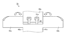
- FIG. 9 is a schematic view showing a cable connection structure according to a modified example 2-1 of the second embodiment.
- FIG. 10 is a schematic view showing a cable connection structure according to a modified example 2-1 of the second embodiment.
- FIG. 11 is a cross-sectional view taken along the line CC of the cable connection structure shown in FIG.
- one extension portion is described, but a plurality of extension portions may be provided.
- the cable connection structure 2a according to the present modification 2-1 includes a substrate 30a and an FPC substrate 40a having a plurality of lead terminals 42 connected to the substrate 30a.
- the substrate 30a has a substantially rectangular shape made of, for example, a semiconductor or a glass epoxy resin, and is connected to an electric circuit or the electric circuit, and a plurality of electrodes 31a provided on one surface are formed.
- the FPC board 40a is made of a bendable insulating film, and is connected to the circuit formation portion 41a, which is a substantially rectangular formation region for forming an electric circuit, etc., and the circuit formation portion 41a, and a plurality of protruding from one end of the circuit formation portion 41a And a lead terminal 42. Further, the FPC board 40a is made of a bendable insulating film, and provided with two extension portions 43a and 43b extending from the circuit forming portion 41a.
- the electrode 31a and the lead terminal 42 are electrically connected by, for example, a conductive bonding material such as solder. Further, as in ultrasonic bonding, electrodes may be metal-bonded to be electrically connected.
- the two extension parts 43a and 43b are from the side surface perpendicular to the side surface of the circuit forming portion 41a from which the lead terminals 42 project. Each extends along the arrangement direction. Further, the distance in the arrangement direction from the base end of the two extension portions 43a and 43b is at least the extension portion 43a or the extension portion 43b of the electrode 31a or the lead terminal 42 as in the second embodiment described above. Is provided so as to be equal to or more than the distance from the proximal end to which the end of the member extends. At this time, it is preferable that the distance be determined in consideration of the thickness of the electrode 31 a and the lead terminal 42.
- the length orthogonal to the arrangement direction can cover the electrode 31a and the lead terminal 42 in a state where the electrode 31a and the lead terminal 42 are connected (fixed). It is.
- the two extension portions 43a and 43b are each bent from the base end to cover the surface of the substrate 30a.
- one of the extension parts (for example, the extension part 43a) covers the surface of the substrate 30a on which the electrode 31a and the lead terminal 42 are disposed.
- the other extension (for example, the extension 43b) covers the rear surface of the surface on which the electrode 31a of the substrate 30a and the lead terminal 42 are disposed (see FIG. 11).
- the respective extension portions 43a and 43b and the substrate 30a are fixed with an adhesive, and the ground electrode is provided on the outer surface side. Since the positional relationship between the recessed portions 43a and 43b and the substrate 30a is fixed, the distance between each lead terminal 42 and the ground electrode formed in the extended portions 43a and 43b can be appropriately maintained. The interference between the signals transmitted by the lead terminals 42 can be suppressed, and the necessary insulation can be secured even when the outside of the cable connection structure 2a is damaged.
- extension part 43a and 43b one extension part having a length corresponding to the two extension parts is provided to the substrate. It may be wound. Thus, the outer periphery of the substrate can be covered with the extension portion.
- FIG. 12 is a perspective view schematically showing a cable connection structure which is a modified example 2-2 of the second embodiment.
- FIG. 13 is a schematic view showing the configuration of a substrate of the cable connection structure shown in FIG.
- FIG. 14 is an exploded perspective view schematically showing a cable connection structure which is a modified example 2-2 of the second embodiment.
- FIG. 15 is a perspective view schematically showing a cable connection structure which is a modification 2-2 of the second embodiment.
- the main surface of the substrate and the main surface of the FPC substrate are described as being substantially parallel to each other, but the main surface of the substrate and the main surface of the FPC substrate are orthogonal to each other It may be
- the cable connection structure 2b according to the modification 2-2 includes the substrate 30a described above and an FPC board 40b having a plurality of lead terminals 42a (cables) connected to the substrate 30a.
- the FPC board 40b is made of a bendable insulating film, and is connected to the circuit forming portion 41b, which is a substantially rectangular circuit forming portion in which an electric circuit or the like is formed, and the plurality of leads projecting from one end of the circuit forming portion 41b. And a terminal 42a.
- the FPC board 40b is made of a bendable insulating film, and is provided with an extending portion 43c extending from one end of the circuit forming portion 41b.
- the lead terminal 42a is made of, for example, copper, and the surface may be plated with nickel or gold.
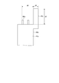
- the extending portion 43c extends along a direction perpendicular to the arranging direction of the lead terminals 42a, and the distance d3 of the circuit forming portion 41b in the protruding direction from the protruding end portion of the lead terminal 42a is at least a lead terminal of the extending portion 43c. It extends so as to be equal to or longer than the distance d4 from the end on the side 42a to the end of the lead terminal 42a far from the extension 43c. Further, the protruding length d5 from the base end of the extending portion 43c is a length capable of covering the lead terminal 42a and the electrode 31a when it is bent.
- the electrode 31a and the lead terminal 42a are electrically connected by a conductive bonding material such as solder, for example. Further, as in ultrasonic bonding, electrodes may be metal-bonded to be electrically connected. At this time, as shown in FIG. 14, the lead terminal 42a is bent in a direction orthogonal to the main surface of the circuit forming portion 41b and connected to the electrode 31a.
- the main surface of the extending portion 43c is bent from the base end in a direction orthogonal to the main surface of the circuit forming portion 41b (see FIG. 15). It is bent along the outer edge to cover the electrode 31a and the lead terminal 42a (see FIG. 12).
- the contact portion between the side surface of the substrate 30a and the circuit forming portion 41b of the FPC board 40b be fixed by an adhesive or the like.
- the modification 2-2 in addition to the effect according to the second embodiment described above, it is possible to apply even when the main surface of the substrate 30a and the main surface of the FPC board 40b are not parallel.
- the positional relationship between the extension portion 43c and the substrate 30a is fixed by fixing the extension portion 43c and the substrate 30a with an adhesive and providing a ground electrode at least on the outer surface side of the extension portion 43c.
- each lead terminal 42a and the ground electrode formed in the extending portion 43c can be appropriately maintained, interference between signals transmitted through each lead terminal 42a can be suppressed. Even if there is damage to the outside of the cable connection structure 2b, necessary insulation can be secured.
- FIG. 16 is a schematic view showing the configuration of the transducer module 100 connected to the cable connection structure according to the third embodiment.
- FIG. 17 is a schematic view showing the configuration of the FPC board 50 of the cable connection structure according to the third embodiment.
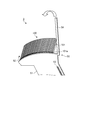
- the transducer module 100 used in the third embodiment as shown in FIG. 16, for example, a plurality of rectangular columnar ultrasonic transducers 101 made of piezoelectric elements are arranged in the direction orthogonal to the longitudinal direction of the ultrasonic transducers 101. Being mounted on the board.
- the side surfaces formed by the arrayed ultrasonic transducers 101 are arc-shaped (convex type).
- Each ultrasonic transducer 101 is provided at one end with an electrode 101a for electrically connecting to, for example, the FPC board 50 shown in FIG.
- the FPC board 50 is made of a bendable insulating film, and has a circuit forming portion 51 which is a formation region of an electric circuit or the like, a plurality of lead terminals 52 (cables) projecting from one end of the circuit forming portion 51 And an electrode 53 provided on the surface on the other end side of the electrode 51 and connected to the plurality of cables 60 respectively. Further, the FPC board 50 is made of a bendable insulating film and extends from an end near the lead terminal 52 of the circuit forming part 41, and an end near the electrode 53 of the circuit forming part 51. And a second extension 55 extending therefrom.
- the end surface from which the lead terminal 52 protrudes has a curvature equivalent to the curvature of the arc-shaped side surface formed by the plurality of ultrasonic transducers 101.
- the lead terminal 52 is made of, for example, copper, and the surface may be plated with nickel or gold.
- FIG. 18 is a perspective view schematically showing an ultrasonic probe 3 including the cable connection structure according to the third embodiment.
- FIG. 19 is a perspective view schematically showing an ultrasonic probe 3 including the cable connection structure according to the third embodiment.
- the first extending portion 54 is bent so that the main surface is orthogonal to the main surface of the circuit forming portion 51, and then is bent to cover the electrode 101 a and the lead terminal 52.
- the space between the circuit forming portion 51 and the first extension portion 54 is filled with the adhesive and fixed.
- the FPC board 50 and the cable 60 bring the lead wire 61 into contact with the electrode 53 and are electrically connected by, for example, a conductive bonding material such as solder.
- the second extension portion 55 is bent so as to cover the connection portion between the electrode 53 and the conducting wire 61.
- the space between the circuit forming portion 51 and the second extending portion 55 is filled with an adhesive and fixed.
- damage to the lead terminal 52, the electrodes 53 and 101a, and the lead wire 61 can be prevented with a simple configuration, and from the outside Incident noise and radiation noise from the inside can be shielded.
- the circuit forming portion 51 and the first extension portion 54 and the second extension portion 55 are respectively fixed with an adhesive.
- the ground electrode By providing the ground electrode on the outer surface side, the positional relationship between the transducer module 100, the first extension portion 54, the second extension portion 55, and the cable 60 is fixed. Since the distance between the (cable 60) and the ground electrode formed in the first extending portion 54 and the second extending portion 55 can be properly maintained, each lead terminal 52 and each conducting wire 61 (cable 60) can be used. Interference between signals to be transmitted can be suppressed, and necessary insulation can be secured even when damage occurs to the outside of the cable connection structure.
- each connection between the lead terminal and the cable and the electrode can be appropriately combined with any one of the first and second embodiments and the modification described above.
- the transducer module 100 mounting a plurality of rectangular columnar ultrasonic transducers 101 made of piezoelectric elements has been described as an example, but a capacitive ultrasonic transducer (C-MUT; The same function and effect can be obtained as a transducer module 100 equipped with a Capacitive Micromachined Ultrasonic Transducer.
- a capacitive ultrasonic transducer (C-MUT) is adopted, unlike a piezoelectric element having a pair of electrodes in parallel planes, a configuration in which positive and negative electrodes (wiring portions) 101a are disposed on one side and can do.
- the wiring portions on the signal line side and the GND line side can be covered with the extension portion of the present embodiment, and the necessary insulation can be easily ensured.
- the electrode (wiring part) on one surface the visibility can be improved, the wiring condition can be confirmed, and the wiring operation can be facilitated, and the productivity is improved.
- the ultrasound probe 3 according to the third embodiment described above is provided, for example, at the tip of the ultrasound endoscope 210 of the ultrasound endoscope system 200 shown in FIG.
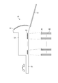
- An ultrasound endoscope system 200 shown in FIG. 20 is configured by an ultrasound endoscope 210, an endoscope observation device 220, an ultrasound observation device 230, a display device 240, and a light source device 250. .
- the ultrasound endoscope 210 is a convex ultrasound endoscope including a convex type transducer module 100 and an imaging unit having an observation optical system and an imaging element configured by a lens or the like. It has a function and an endoscopic observation function.
- the transducer module 100 is realized by the above-described cable connection structure (ultrasound probe 3).
- the endoscopic observation device 220 controls the endoscopic observation function and processes its output signal.
- the ultrasonic observation device 230 controls the ultrasonic observation function and processes the output signal.
- the display device 240 receives each signal from, for example, the endoscopic observation device 220 and the ultrasonic observation device 230, and appropriately displays at least one of an endoscopic image or an ultrasonic tomographic image.
- the light source device 250 includes a light source (not shown) for supplying illumination light for performing endoscopic observation.
- the ultrasound endoscope system 200 includes a video cable 260 and an ultrasound cable 270 that connect the ultrasound endoscope 210, the endoscope observation device 220, the ultrasound observation device 230, the display device 240, and the light source device 250, respectively.
- a light source cable 280 is also included in the ultrasound endoscope system 200.
- the ultrasound endoscope 210 is inserted into the body and outputs an ultrasound signal in the body, and an insertion portion 211 for acquiring an ultrasound signal reflected in the body, and is provided continuously with the proximal end side of the insertion portion 211
- the operation unit 212 is configured, and the universal cable 213 extending from the side of the operation unit 212 is configured.
- the universal cable 213 is provided at an end different from the operation unit 212, and has a connector 214 that connects to the video cable 260, the ultrasonic cable 270, and the light source cable 280, respectively.
- the insertion portion 211 is configured by connecting a distal end hard portion 211 a formed of a hard member, a bendable curved portion 211 b, and a flexible flexible tube portion 211 c having flexibility, sequentially from the distal end side. .
- the proximal end of the flexible tube portion 211 c is continuously provided on the distal end side of the operation portion 212.
- the vibrator module 100 described above is disposed in the distal end rigid portion 211a.
- the operation unit 212 is provided with a treatment tool insertion port 212a for introducing a puncture needle or the like, which will be described later, which is a treatment tool, into the body.
- a treatment tool insertion path is provided inside the insertion portion 211, and the treatment tool insertion port 212a is an insertion port of the treatment tool insertion path.
- the ultrasonic endoscope 210 and the endoscopic observation device 220 are electrically connected by a video cable 260 connected to the connector portion 214.
- the ultrasound endoscope 210 and the ultrasound observation apparatus 230 are electrically connected by an ultrasound cable 270 connected to the connector portion 214.
- the light source cable 280 is an optical fiber cable, and the ultrasound endoscope 210 and the light source device 250 are configured to receive the illumination light from the light source of the light source device 250 by the light source cable 280 connected to the connector portion 214. Lead to
- the ultrasonic probe 3 for transmitting and receiving ultrasonic waves is provided at the tip of the insertion portion 211, and the insertion portion 211 is inserted into the body of the subject.
- An ultrasonic image of an obtained organ or the like is displayed on the display unit 241 of the display device 240, and an in-vivo image captured by the endoscope observation function is displayed on the display unit 241, thereby observing, diagnosing, etc. It is possible to do.
- the cable connection structure, the ultrasonic probe, and the ultrasonic endoscope system according to the present invention are useful for simply forming a shield structure and suppressing signal interference between cables. .
Landscapes
- Health & Medical Sciences (AREA)
- Life Sciences & Earth Sciences (AREA)
- General Health & Medical Sciences (AREA)
- Physics & Mathematics (AREA)
- Pathology (AREA)
- Engineering & Computer Science (AREA)
- Public Health (AREA)
- Medical Informatics (AREA)
- Veterinary Medicine (AREA)
- Animal Behavior & Ethology (AREA)
- Surgery (AREA)
- Biophysics (AREA)
- Nuclear Medicine, Radiotherapy & Molecular Imaging (AREA)
- Radiology & Medical Imaging (AREA)
- Molecular Biology (AREA)
- Biomedical Technology (AREA)
- Heart & Thoracic Surgery (AREA)
- General Physics & Mathematics (AREA)
- Analytical Chemistry (AREA)
- Biochemistry (AREA)
- Chemical & Material Sciences (AREA)
- Immunology (AREA)
- Microelectronics & Electronic Packaging (AREA)
- Gynecology & Obstetrics (AREA)
- Ultra Sonic Daignosis Equipment (AREA)
- Investigating Or Analyzing Materials By The Use Of Ultrasonic Waves (AREA)
- Coupling Device And Connection With Printed Circuit (AREA)
- Endoscopes (AREA)
Priority Applications (1)
| Application Number | Priority Date | Filing Date | Title |
|---|---|---|---|
| US14/494,980 US10158188B2 (en) | 2012-03-27 | 2014-09-24 | Cable connection structure, ultrasonic probe, and ultrasonic endoscope system |
Applications Claiming Priority (2)
| Application Number | Priority Date | Filing Date | Title |
|---|---|---|---|
| JP2012072197A JP5973761B2 (ja) | 2012-03-27 | 2012-03-27 | ケーブル接続構造 |
| JP2012-072197 | 2012-03-27 |
Related Child Applications (1)
| Application Number | Title | Priority Date | Filing Date |
|---|---|---|---|
| US14/494,980 Continuation US10158188B2 (en) | 2012-03-27 | 2014-09-24 | Cable connection structure, ultrasonic probe, and ultrasonic endoscope system |
Publications (1)
| Publication Number | Publication Date |
|---|---|
| WO2013145894A1 true WO2013145894A1 (ja) | 2013-10-03 |
Family
ID=49259178
Family Applications (1)
| Application Number | Title | Priority Date | Filing Date |
|---|---|---|---|
| PCT/JP2013/053118 Ceased WO2013145894A1 (ja) | 2012-03-27 | 2013-02-08 | ケーブル接続構造、超音波探触子および超音波内視鏡システム |
Country Status (3)
| Country | Link |
|---|---|
| US (1) | US10158188B2 (https=) |
| JP (1) | JP5973761B2 (https=) |
| WO (1) | WO2013145894A1 (https=) |
Families Citing this family (12)
| Publication number | Priority date | Publication date | Assignee | Title |
|---|---|---|---|---|
| US11166629B2 (en) * | 2016-09-29 | 2021-11-09 | Nanosurgery Technology Corporation | Video needle syringe |
| JP7013661B2 (ja) * | 2017-03-22 | 2022-02-01 | セイコーエプソン株式会社 | 超音波デバイスユニット、超音波探触子、及び超音波装置 |
| US10925628B2 (en) | 2017-09-18 | 2021-02-23 | Novuson Surgical, Inc. | Tissue engagement apparatus for theapeutic ultrasound apparatus and method |
| WO2019146331A1 (ja) * | 2018-01-29 | 2019-08-01 | 富士フイルム株式会社 | 超音波内視鏡及び超音波内視鏡の製造方法 |
| WO2020012566A1 (ja) * | 2018-07-10 | 2020-01-16 | オリンパス株式会社 | ケーブル接続構造体、内視鏡およびケーブル接続構造体の製造方法 |
| JP7109654B2 (ja) * | 2019-03-29 | 2022-07-29 | オリンパス株式会社 | 超音波振動子、超音波内視鏡及び超音波振動子の製造方法 |
| JP2022169817A (ja) * | 2019-09-30 | 2022-11-10 | Agc株式会社 | 高周波シールド構造 |
| US12494521B2 (en) | 2020-03-19 | 2025-12-09 | Sanyo Electric Co., Ltd. | Voltage detection line and voltage detection line module |
| CN111537840A (zh) * | 2020-06-15 | 2020-08-14 | 刘大永 | 一种具有无源超声监测功能的t型电缆接头绝缘后堵 |
| JP7370949B2 (ja) * | 2020-09-08 | 2023-10-30 | 富士フイルム株式会社 | 超音波内視鏡 |
| JP7324180B2 (ja) * | 2020-09-08 | 2023-08-09 | 富士フイルム株式会社 | 超音波内視鏡 |
| WO2023233458A1 (ja) * | 2022-05-30 | 2023-12-07 | 住友電気工業株式会社 | 接続構造及び接続構造の製造方法 |
Citations (6)
| Publication number | Priority date | Publication date | Assignee | Title |
|---|---|---|---|---|
| JPS4910082U (https=) * | 1972-04-28 | 1974-01-28 | ||
| JPS58116262U (ja) * | 1982-01-30 | 1983-08-08 | 日本メクトロン株式会社 | シ−ルド構造を備えたフレキシブル回路基板 |
| JPS61117265U (https=) * | 1984-12-29 | 1986-07-24 | ||
| JPS6263979U (https=) * | 1985-10-11 | 1987-04-21 | ||
| JP2000067968A (ja) * | 1998-08-19 | 2000-03-03 | Tokai Rika Co Ltd | コネクタ装置及びその接続方法 |
| JP2003309339A (ja) * | 2002-04-17 | 2003-10-31 | Hitachi Cable Ltd | 極細ケーブルの接続基板及び接続方法 |
Family Cites Families (13)
| Publication number | Priority date | Publication date | Assignee | Title |
|---|---|---|---|---|
| JPH077931Y2 (ja) | 1989-02-22 | 1995-03-01 | ジーイー横河メディカルシステム株式会社 | 超音波探触子 |
| JPH03151942A (ja) | 1989-11-09 | 1991-06-28 | Toshiba Corp | 超音波診断装置のメカニカルセクタプローブ |
| GB8926861D0 (en) * | 1989-11-28 | 1990-01-17 | Alcan Int Ltd | Improvements in or relating to aluminium alloys |
| JP2701563B2 (ja) * | 1991-03-18 | 1998-01-21 | 日本電気株式会社 | 表示素子の外部リード接続基板実装構造 |
| JPH05136593A (ja) | 1991-03-19 | 1993-06-01 | Fujitsu Ltd | シールド構造 |
| US5262590A (en) * | 1992-04-27 | 1993-11-16 | Sheldahl, Inc. | Impedance controlled flexible circuits with fold-over shields |
| US5375321A (en) * | 1993-03-30 | 1994-12-27 | United States Department Of Energy | Method for fabricating fan-fold shielded electrical leads |
| JP3234743B2 (ja) | 1995-05-30 | 2001-12-04 | シャープ株式会社 | 半導体部品実装型フレキシブルプリント基板 |
| JP2001357916A (ja) * | 2000-06-13 | 2001-12-26 | Yazaki Corp | フラット回路体の接続構造 |
| US20020189854A1 (en) * | 2001-04-10 | 2002-12-19 | Crumly William R. | Design for long fatigue life in flexible circuits |
| JP4391717B2 (ja) * | 2002-01-09 | 2009-12-24 | 富士通マイクロエレクトロニクス株式会社 | コンタクタ及びその製造方法並びにコンタクト方法 |
| WO2005120130A1 (ja) * | 2004-06-03 | 2005-12-15 | Olympus Corporation | 静電容量型超音波振動子とその製造方法、静電容量型超音波プローブ |
| JP4657357B2 (ja) * | 2009-07-21 | 2011-03-23 | オリンパス株式会社 | 超音波内視鏡 |
-
2012
- 2012-03-27 JP JP2012072197A patent/JP5973761B2/ja active Active
-
2013
- 2013-02-08 WO PCT/JP2013/053118 patent/WO2013145894A1/ja not_active Ceased
-
2014
- 2014-09-24 US US14/494,980 patent/US10158188B2/en active Active
Patent Citations (6)
| Publication number | Priority date | Publication date | Assignee | Title |
|---|---|---|---|---|
| JPS4910082U (https=) * | 1972-04-28 | 1974-01-28 | ||
| JPS58116262U (ja) * | 1982-01-30 | 1983-08-08 | 日本メクトロン株式会社 | シ−ルド構造を備えたフレキシブル回路基板 |
| JPS61117265U (https=) * | 1984-12-29 | 1986-07-24 | ||
| JPS6263979U (https=) * | 1985-10-11 | 1987-04-21 | ||
| JP2000067968A (ja) * | 1998-08-19 | 2000-03-03 | Tokai Rika Co Ltd | コネクタ装置及びその接続方法 |
| JP2003309339A (ja) * | 2002-04-17 | 2003-10-31 | Hitachi Cable Ltd | 極細ケーブルの接続基板及び接続方法 |
Also Published As
| Publication number | Publication date |
|---|---|
| US10158188B2 (en) | 2018-12-18 |
| JP2013206617A (ja) | 2013-10-07 |
| US20150011891A1 (en) | 2015-01-08 |
| JP5973761B2 (ja) | 2016-08-23 |
Similar Documents
| Publication | Publication Date | Title |
|---|---|---|
| JP5973761B2 (ja) | ケーブル接続構造 | |
| EP2591731B1 (en) | Ultrasound transducer unit, ultrasound endoscope | |
| US10312566B2 (en) | Cable connection structure and endoscope device | |
| US11317897B2 (en) | Ultrasonic endoscope and method for manufacturing same | |
| US10653306B2 (en) | Electronic circuit unit, imaging unit, and endoscope | |
| CN105451664B (zh) | 超声波内窥镜顶端部 | |
| US20180070803A1 (en) | Imaging device and endoscope system | |
| US20160028926A1 (en) | Endoscope apparatus | |
| US8298008B2 (en) | Mounting assembly and cable assembly | |
| WO2018003322A1 (ja) | 超音波内視鏡 | |
| CN107530056B (zh) | 内窥镜用连接器 | |
| JP6132963B2 (ja) | ケーブル接続構造、超音波探触子および超音波内視鏡システム | |
| JP6033521B1 (ja) | 超音波プローブ | |
| JP4376533B2 (ja) | 超音波探触子 | |
| US10517465B2 (en) | Cable connection structure and endoscope apparatus | |
| US20170144194A1 (en) | Ultrasound transducer and ultrasound endoscope | |
| JP6099541B2 (ja) | 内視鏡及び内視鏡の製造方法 | |
| JP7324181B2 (ja) | 超音波内視鏡 | |
| JP7324180B2 (ja) | 超音波内視鏡 | |
| JP7395277B2 (ja) | 信号伝送配線接続ユニット、内視鏡、信号伝送配線接続ユニットの製造方法および超音波振動子モジュール |
Legal Events
| Date | Code | Title | Description |
|---|---|---|---|
| 121 | Ep: the epo has been informed by wipo that ep was designated in this application |
Ref document number: 13769528 Country of ref document: EP Kind code of ref document: A1 |
|
| NENP | Non-entry into the national phase |
Ref country code: DE |
|
| 122 | Ep: pct application non-entry in european phase |
Ref document number: 13769528 Country of ref document: EP Kind code of ref document: A1 |