WO2013145160A1 - 金属酸化膜の製造方法および金属酸化膜 - Google Patents
金属酸化膜の製造方法および金属酸化膜 Download PDFInfo
- Publication number
- WO2013145160A1 WO2013145160A1 PCT/JP2012/058153 JP2012058153W WO2013145160A1 WO 2013145160 A1 WO2013145160 A1 WO 2013145160A1 JP 2012058153 W JP2012058153 W JP 2012058153W WO 2013145160 A1 WO2013145160 A1 WO 2013145160A1
- Authority
- WO
- WIPO (PCT)
- Prior art keywords
- metal oxide
- oxide film
- dopant
- substrate
- resistance
- Prior art date
- Legal status (The legal status is an assumption and is not a legal conclusion. Google has not performed a legal analysis and makes no representation as to the accuracy of the status listed.)
- Ceased
Links
Images



Classifications
-
- C—CHEMISTRY; METALLURGY
- C23—COATING METALLIC MATERIAL; COATING MATERIAL WITH METALLIC MATERIAL; CHEMICAL SURFACE TREATMENT; DIFFUSION TREATMENT OF METALLIC MATERIAL; COATING BY VACUUM EVAPORATION, BY SPUTTERING, BY ION IMPLANTATION OR BY CHEMICAL VAPOUR DEPOSITION, IN GENERAL; INHIBITING CORROSION OF METALLIC MATERIAL OR INCRUSTATION IN GENERAL
- C23C—COATING METALLIC MATERIAL; COATING MATERIAL WITH METALLIC MATERIAL; SURFACE TREATMENT OF METALLIC MATERIAL BY DIFFUSION INTO THE SURFACE, BY CHEMICAL CONVERSION OR SUBSTITUTION; COATING BY VACUUM EVAPORATION, BY SPUTTERING, BY ION IMPLANTATION OR BY CHEMICAL VAPOUR DEPOSITION, IN GENERAL
- C23C18/00—Chemical coating by decomposition of either liquid compounds or solutions of the coating forming compounds, without leaving reaction products of surface material in the coating; Contact plating
- C23C18/02—Chemical coating by decomposition of either liquid compounds or solutions of the coating forming compounds, without leaving reaction products of surface material in the coating; Contact plating by thermal decomposition
- C23C18/12—Chemical coating by decomposition of either liquid compounds or solutions of the coating forming compounds, without leaving reaction products of surface material in the coating; Contact plating by thermal decomposition characterised by the deposition of inorganic material other than metallic material
- C23C18/1204—Chemical coating by decomposition of either liquid compounds or solutions of the coating forming compounds, without leaving reaction products of surface material in the coating; Contact plating by thermal decomposition characterised by the deposition of inorganic material other than metallic material inorganic material, e.g. non-oxide and non-metallic such as sulfides, nitrides based compounds
- C23C18/1208—Oxides, e.g. ceramics
- C23C18/1216—Metal oxides
-
- C—CHEMISTRY; METALLURGY
- C23—COATING METALLIC MATERIAL; COATING MATERIAL WITH METALLIC MATERIAL; CHEMICAL SURFACE TREATMENT; DIFFUSION TREATMENT OF METALLIC MATERIAL; COATING BY VACUUM EVAPORATION, BY SPUTTERING, BY ION IMPLANTATION OR BY CHEMICAL VAPOUR DEPOSITION, IN GENERAL; INHIBITING CORROSION OF METALLIC MATERIAL OR INCRUSTATION IN GENERAL
- C23C—COATING METALLIC MATERIAL; COATING MATERIAL WITH METALLIC MATERIAL; SURFACE TREATMENT OF METALLIC MATERIAL BY DIFFUSION INTO THE SURFACE, BY CHEMICAL CONVERSION OR SUBSTITUTION; COATING BY VACUUM EVAPORATION, BY SPUTTERING, BY ION IMPLANTATION OR BY CHEMICAL VAPOUR DEPOSITION, IN GENERAL
- C23C18/00—Chemical coating by decomposition of either liquid compounds or solutions of the coating forming compounds, without leaving reaction products of surface material in the coating; Contact plating
- C23C18/02—Chemical coating by decomposition of either liquid compounds or solutions of the coating forming compounds, without leaving reaction products of surface material in the coating; Contact plating by thermal decomposition
- C23C18/12—Chemical coating by decomposition of either liquid compounds or solutions of the coating forming compounds, without leaving reaction products of surface material in the coating; Contact plating by thermal decomposition characterised by the deposition of inorganic material other than metallic material
- C23C18/125—Process of deposition of the inorganic material
- C23C18/1258—Spray pyrolysis
-
- C—CHEMISTRY; METALLURGY
- C23—COATING METALLIC MATERIAL; COATING MATERIAL WITH METALLIC MATERIAL; CHEMICAL SURFACE TREATMENT; DIFFUSION TREATMENT OF METALLIC MATERIAL; COATING BY VACUUM EVAPORATION, BY SPUTTERING, BY ION IMPLANTATION OR BY CHEMICAL VAPOUR DEPOSITION, IN GENERAL; INHIBITING CORROSION OF METALLIC MATERIAL OR INCRUSTATION IN GENERAL
- C23C—COATING METALLIC MATERIAL; COATING MATERIAL WITH METALLIC MATERIAL; SURFACE TREATMENT OF METALLIC MATERIAL BY DIFFUSION INTO THE SURFACE, BY CHEMICAL CONVERSION OR SUBSTITUTION; COATING BY VACUUM EVAPORATION, BY SPUTTERING, BY ION IMPLANTATION OR BY CHEMICAL VAPOUR DEPOSITION, IN GENERAL
- C23C18/00—Chemical coating by decomposition of either liquid compounds or solutions of the coating forming compounds, without leaving reaction products of surface material in the coating; Contact plating
- C23C18/02—Chemical coating by decomposition of either liquid compounds or solutions of the coating forming compounds, without leaving reaction products of surface material in the coating; Contact plating by thermal decomposition
- C23C18/12—Chemical coating by decomposition of either liquid compounds or solutions of the coating forming compounds, without leaving reaction products of surface material in the coating; Contact plating by thermal decomposition characterised by the deposition of inorganic material other than metallic material
- C23C18/125—Process of deposition of the inorganic material
- C23C18/1291—Process of deposition of the inorganic material by heating of the substrate
-
- C—CHEMISTRY; METALLURGY
- C23—COATING METALLIC MATERIAL; COATING MATERIAL WITH METALLIC MATERIAL; CHEMICAL SURFACE TREATMENT; DIFFUSION TREATMENT OF METALLIC MATERIAL; COATING BY VACUUM EVAPORATION, BY SPUTTERING, BY ION IMPLANTATION OR BY CHEMICAL VAPOUR DEPOSITION, IN GENERAL; INHIBITING CORROSION OF METALLIC MATERIAL OR INCRUSTATION IN GENERAL
- C23C—COATING METALLIC MATERIAL; COATING MATERIAL WITH METALLIC MATERIAL; SURFACE TREATMENT OF METALLIC MATERIAL BY DIFFUSION INTO THE SURFACE, BY CHEMICAL CONVERSION OR SUBSTITUTION; COATING BY VACUUM EVAPORATION, BY SPUTTERING, BY ION IMPLANTATION OR BY CHEMICAL VAPOUR DEPOSITION, IN GENERAL
- C23C18/00—Chemical coating by decomposition of either liquid compounds or solutions of the coating forming compounds, without leaving reaction products of surface material in the coating; Contact plating
- C23C18/02—Chemical coating by decomposition of either liquid compounds or solutions of the coating forming compounds, without leaving reaction products of surface material in the coating; Contact plating by thermal decomposition
- C23C18/12—Chemical coating by decomposition of either liquid compounds or solutions of the coating forming compounds, without leaving reaction products of surface material in the coating; Contact plating by thermal decomposition characterised by the deposition of inorganic material other than metallic material
- C23C18/125—Process of deposition of the inorganic material
- C23C18/1295—Process of deposition of the inorganic material with after-treatment of the deposited inorganic material
-
- H—ELECTRICITY
- H01—ELECTRIC ELEMENTS
- H01B—CABLES; CONDUCTORS; INSULATORS; SELECTION OF MATERIALS FOR THEIR CONDUCTIVE, INSULATING OR DIELECTRIC PROPERTIES
- H01B1/00—Conductors or conductive bodies characterised by the conductive materials; Selection of materials as conductors
- H01B1/06—Conductors or conductive bodies characterised by the conductive materials; Selection of materials as conductors mainly consisting of other non-metallic substances
- H01B1/08—Conductors or conductive bodies characterised by the conductive materials; Selection of materials as conductors mainly consisting of other non-metallic substances oxides
-
- H—ELECTRICITY
- H10—SEMICONDUCTOR DEVICES; ELECTRIC SOLID-STATE DEVICES NOT OTHERWISE PROVIDED FOR
- H10F—INORGANIC SEMICONDUCTOR DEVICES SENSITIVE TO INFRARED RADIATION, LIGHT, ELECTROMAGNETIC RADIATION OF SHORTER WAVELENGTH OR CORPUSCULAR RADIATION
- H10F71/00—Manufacture or treatment of devices covered by this subclass
- H10F71/138—Manufacture of transparent electrodes, e.g. transparent conductive oxides [TCO] or indium tin oxide [ITO] electrodes
-
- Y—GENERAL TAGGING OF NEW TECHNOLOGICAL DEVELOPMENTS; GENERAL TAGGING OF CROSS-SECTIONAL TECHNOLOGIES SPANNING OVER SEVERAL SECTIONS OF THE IPC; TECHNICAL SUBJECTS COVERED BY FORMER USPC CROSS-REFERENCE ART COLLECTIONS [XRACs] AND DIGESTS
- Y02—TECHNOLOGIES OR APPLICATIONS FOR MITIGATION OR ADAPTATION AGAINST CLIMATE CHANGE
- Y02E—REDUCTION OF GREENHOUSE GAS [GHG] EMISSIONS, RELATED TO ENERGY GENERATION, TRANSMISSION OR DISTRIBUTION
- Y02E10/00—Energy generation through renewable energy sources
- Y02E10/50—Photovoltaic [PV] energy
Definitions
- the present invention relates to a method for manufacturing a metal oxide film and a metal oxide film, and can be applied to a method for manufacturing a metal oxide film used in, for example, a solar cell or an electronic device.
- a method for forming a metal oxide film used in solar cells, electronic devices, etc. for example, a MOCVD (Metal Organic Chemical Deposition) method using a vacuum, a sputtering method, or the like is employed.
- MOCVD Metal Organic Chemical Deposition
- the metal oxide films produced by these metal oxide film manufacturing methods have excellent film characteristics.
- the resistance of the transparent conductive film is low, and even if the transparent conductive film after the production is subjected to heat treatment, The resistance of the transparent conductive film does not increase.
- Patent Document 1 exists as a prior document relating to the formation of a zinc oxide film by the MOCVD method.
- Patent Document 2 exists as a prior document relating to the formation of a zinc oxide film by sputtering.
- the MODVD method is inferior in terms of convenience because it requires high cost to realize the method and requires the use of an unstable material in the air.
- a metal oxide film having a laminated structure is produced by sputtering, a plurality of apparatuses are required, which increases the cost of the apparatus. Therefore, a metal oxide film manufacturing method capable of producing a low-resistance metal oxide film at low cost is desired.
- a method for producing a metal oxide film according to the present invention includes: (A) a step of spraying a solution containing zinc on a substrate placed in a non-vacuum; In the step (A), a step of spraying a dopant solution containing a dopant onto the substrate; and (C) a metal oxide film formed on the substrate by the step (A) and the step (B). And a step of subjecting the film to a low resistance treatment without restructuring the crystal of the metal oxide film, and the zinc supplied to the substrate in the steps (A) and (B) The molar concentration of the dopant supplied to the substrate with respect to the molar concentration is not less than a predetermined value.
- step (A) a step of spraying a solution containing zinc on a substrate placed under non-vacuum, and (B) in the step (A), A step of spraying a dopant solution containing a dopant on the substrate; and (C) the metal oxide film on the metal oxide film formed on the substrate by the step (A) and the step (B).
- step (C) the metal oxide film on the metal oxide film formed on the substrate by the step (A) and the step (B).
- a step of reducing resistance without restructuring the crystal and supplying the substrate with respect to the molar concentration of the zinc supplied to the substrate in the steps (A) and (B).
- the molar concentration of the dopant is not less than a predetermined value.
- the metal oxide film is formed on the substrate in a non-vacuum state. Therefore, the cost required for the film formation process (film formation apparatus cost) can be reduced, and convenience can be improved.
- the resistance reduction treatment is performed on the metal oxide film after film formation. Therefore, even when a metal oxide film is formed on the substrate under non-vacuum, it is possible to reduce the resistance of the metal oxide film (the metal oxide film formed under vacuum). The resistance of the metal oxide film formed under non-vacuum can be reduced to the same extent as the resistance).
- the metal oxide film is formed on the substrate by supplying (spraying) zinc and dopant to the substrate.
- (dopant) / Zn molar concentration ratio is set to the predetermined value or more. Therefore, even if a long period of time has elapsed after the low resistance treatment, the resistance of the metal oxide film subjected to the low resistance treatment can be prevented from increasing.
- a film forming process is performed under non-vacuum (atmospheric pressure).
- the metal oxide film containing zinc (Zn) formed under the non-vacuum (atmospheric pressure) has a high resistance immediately after the film formation. Therefore, the metal oxide film immediately after the film formation is subjected to low resistance treatment without high temperature treatment (that is, energy higher than the band gap of the metal oxide film without restructuring the crystal of the metal oxide film). Is applied to the metal oxide film immediately after the film formation).
- the low resistance treatment for example, ultraviolet irradiation on the metal oxide film can be employed.
- the low resistance of the metal oxide film is realized by the low resistance treatment immediately after the low resistance treatment.
- the resistance of the metal oxide film is increased again after a lapse of time from the low resistance treatment.
- the inventors have found.
- the molar concentration of dopant supplied to the substrate relative to the molar concentration of zinc supplied to the substrate is set to a predetermined value or higher (in other words, supplied to the substrate).
- the inventors have also found that the increase in resistance of the film can be suppressed.
- a solution 7 containing at least zinc is prepared.
- an organic solvent such as ether or alcohol is employed as the solvent of the solution 7.
- the produced solution 7 is filled in the container 3A as shown in FIG.
- water H 2 O
- the vessel 3B is filled with the oxidation source 6 as shown in FIG.
- oxygen, ozone, hydrogen peroxide, N 2 O, NO 2 and the like can be used as the oxidation source 6, but water is desirable from the viewpoint of low cost and easy handling (hereinafter, the oxidation source 6 is Suppose it is water).
- the dopant solution 5 containing a dopant is produced.
- a dopant solution 5 containing boron (B) is prepared.
- a boric acid (H 3 BO 3 ) solution can be employed.
- the produced dopant solution 5 is filled in a container 3C as shown in FIG.
- the dopant solution 5, the oxidation source 6 and the solution 7 are respectively misted.
- An atomizer 4A is disposed at the bottom of the container 3A
- an atomizer 4B is disposed at the bottom of the container 3B
- an atomizer 4C is disposed at the bottom of the container 3C.
- the atomizer 4A mists the solution 7 in the container 3A
- the atomizer 4B mists the oxidation source 6 in the container 3B
- the atomizer 4C mists the dopant solution 5 in the container 3C.
- the misted solution 7 is supplied to the nozzle 8 through the path L1
- the misted oxidation source 6 is supplied to the nozzle 8 through the path L2
- the misted dopant solution 5 passes through the path L3.
- the route L1, the route L2, and the route L3 are separate passages.
- the molar concentration of the dopant supplied to the substrate 1 (that is, the dopant / Zn molar concentration ratio) with respect to the molar concentration of zinc supplied to the substrate 1 needs to be a predetermined value or more.
- the molar concentration ratio includes the carrier gas supply amount (liter / minute) of the solution 7 to the nozzle 8 (or substrate 1), the molar concentration of zinc in the solution 7, and the nozzle solution 8 of the dopant solution 5 to the nozzle 8 (or substrate 1). It can be adjusted by adjusting the carrier gas supply amount (liter / min) and the molar concentration of the dopant in the dopant solution 5.
- the substrate 1 is placed on the heater 2.
- the substrate 1 is placed under non-vacuum (atmospheric pressure).
- the misted solution 7, the misted oxidation source 6 and the misted dopant solution 5 are separately and independently supplied through the nozzle 8.
- Spraying (supplying) from the nozzle is separately and independently supplied from the nozzle.
- the substrate 1 is heated to, for example, about 200 ° C. by the heater 2.
- a metal oxide film (zinc oxide film which is a transparent conductive film) having a predetermined thickness is formed on the substrate 1 placed under non-vacuum (atmospheric pressure).
- the deposited metal oxide film contains not only zinc but also a dopant with respect to zinc.
- the resistance of a metal oxide film formed under non-vacuum is higher than that of a metal oxide film formed under vacuum such as sputtering. Therefore, in the method for manufacturing a metal oxide film according to the present invention, as described above, a resistance reduction process is performed that gives energy higher than the band gap of the metal oxide film without restructuring the crystal of the metal oxide film.
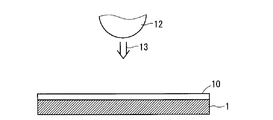
- an ultraviolet lamp 12 or the like is used on the entire main surface of the metal oxide film 10 formed on the substrate 1. Irradiate ultraviolet rays 13. Irradiation with the ultraviolet rays 13 can reduce the resistance (resistivity) of the metal oxide film 10.
- the resistance of the metal oxide film when the metal oxide film is non-doped, for example, even if the resistance reduction treatment is performed on the formed metal oxide film, the resistance increases with time. . As a result, the resistance of the metal oxide film returns to the resistance value before the low resistance treatment.
- the dopant is contained in the metal oxide film, and the dopant / Zn molar concentration ratio at the time of supplying the dopant and zinc to the substrate 1 is a predetermined value or more, the metal oxide film.
- the resistance reduction treatment is performed and then time passes, it is possible to suppress the resistance increase of the metal oxide film.
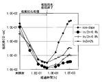
- FIG. 3 is experimental data showing the effect of suppressing the increase in resistance.
- FIG. 3 shows a time-series change in resistivity of each metal oxide film. More specifically, FIG. 3 shows a time-series change in the resistivity of each metal oxide film after ultraviolet irradiation (resistance reduction treatment) and after the ultraviolet irradiation.
- the vertical axis in FIG. 3 is resistivity ( ⁇ ⁇ cm), and the horizontal axis in FIG. 3 is time (h).
- a non-doped metal oxide film containing zinc and a plurality of metal oxide films containing a dopant and zinc are measurement targets.
- the dopant is boron.
- 3 shows a metal oxide film having a B / Zn molar concentration ratio of 0.2% when supplying zinc and boron to the substrate 1 as a plurality of metal oxide films containing a dopant and zinc.
- a metal oxide film having a B / Zn molar concentration ratio of 0.4% when supplying zinc and boron to B, and a B / Zn molar concentration ratio of 0.8% when supplying zinc and boron to substrate 1 are 0.8%.
- 1 shows a metal oxide film and a metal oxide film having a B / Zn molar concentration ratio of 1.8% when zinc and boron are supplied to the substrate 1.
- the deposition temperature of all the metal oxide films described above is 200 ° C.
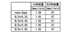
- Each metal oxide film is formed in the film forming apparatus shown in FIG. 1, and the film forming conditions are as shown in FIG.
- the supply amount of zinc to the substrate 1 is 1.26 m (mm) mol / min, and the supply amount of oxidant (water) to the substrate 1 is 67 mmol / min.
- each metal oxide film having the B / Zn molar concentration ratio of 0.2%, 0.4%, 0.8%, and 1.8% zinc on the substrate 1
- the supply amount is 1.05 mmol / min
- the supply amount of the oxidizing agent (water) to the substrate 1 is 67 mmol / min.
- the resistivity of each metal oxide film is reduced by ultraviolet irradiation (resistance reduction treatment).
- the resistivity of the metal oxide film is increased to a level before ultraviolet irradiation (resistance reduction treatment).
- each metal oxide film having a B / Zn molar concentration ratio of 0.4%, 0.8%, and 1.8% it is assumed that time has elapsed after the end of ultraviolet irradiation (resistance reduction treatment). However, the resistance of the metal oxide film is suppressed and the state of low resistivity is maintained (the resistance of the metal oxide film containing boron as a dopant increases substantially even after a lapse of time. The resistance value after the low resistance treatment is almost maintained).
- the metal oxide film contains boron as a dopant, and the B / Zn molar concentration ratio when supplying zinc and boron to the substrate 1 is 0.4% or more, the metal oxide film Even if time elapses after the above-described resistance reduction treatment is performed, the increase in resistance of the metal oxide film can be suppressed.
- FIG. 5 is another experimental data showing the effect of suppressing the increase in resistance.
- FIG. 5 shows a time-series change in resistivity of each metal oxide film. More specifically, FIG. 5 shows time-series changes in the resistivity of each metal oxide film after ultraviolet irradiation (resistance reduction treatment) and after the ultraviolet irradiation.
- the vertical axis in FIG. 5 is resistivity ( ⁇ ⁇ cm), and the horizontal axis in FIG. 5 is time (h).
- FIG. 5 shows a metal oxide film having a In / Zn molar concentration ratio of 0.4% when supplying zinc and indium to the substrate 1 as a plurality of metal oxide films containing a dopant and zinc.
- Metal oxide film having an In / Zn molar concentration ratio of 0.8% when supplying zinc and indium, and an In / Zn molar concentration ratio of 2.0% when supplying zinc and indium to the substrate 1 The metal oxide film which was was shown.
- the deposition temperature of all the metal oxide films described above is 200 ° C.
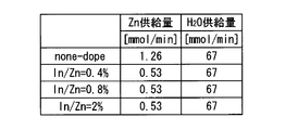
- Each metal oxide film is formed in the film forming apparatus shown in FIG. 1, and the film forming conditions are as shown in FIG.
- the supply amount of zinc to the substrate 1 is 0.53 mmol /
- the supply amount of the oxidizing agent (water) to the substrate 1 is 67 mmol / min.
- the film forming conditions for the non-doped metal oxide film shown in FIG. 6 are the same as the film forming conditions for the other non-doped metal oxide film shown in FIG.
- the resistivity of each metal oxide film is reduced by ultraviolet irradiation (resistance reduction treatment).
- the resistivity of the metal oxide film becomes the ultraviolet irradiation (resistance reduction processing). High resistance to the previous level.
- each metal oxide film having an In / Zn molar concentration ratio of 0.4%, 0.8%, and 2.0% it is assumed that time has elapsed after the end of ultraviolet irradiation (resistance reduction processing).
- the resistance of the metal oxide film is suppressed, and the state of low resistivity is substantially maintained (a metal containing indium as a dopant compared to a metal oxide film containing boron as a dopant).
- the resistance is slightly increased, but the resistance of the metal oxide film containing indium as a dopant is still sufficiently suppressed).
- the metal oxide film contains indium as a dopant, and the In / Zn molar concentration ratio when supplying zinc and indium to the substrate 1 is 0.4% or more, the metal oxide film However, even if time elapses after the resistance reduction treatment is performed, the resistance increase of the metal oxide film can be suppressed.
- FIG. 7 is another experimental data showing the effect of suppressing the increase in resistance.
- FIG. 7 shows a time-series change in resistivity of each metal oxide film. More specifically, FIG. 7 shows time-series changes in the resistivity of each metal oxide film after ultraviolet irradiation (resistance reduction treatment) and after the ultraviolet irradiation.
- the vertical axis in FIG. 7 is resistivity ( ⁇ ⁇ cm), and the horizontal axis in FIG. 7 is time (h).
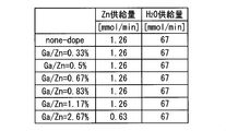
- FIG. 7 shows a metal oxide film having a Ga / Zn molar concentration ratio of 0.33% when supplying zinc and gallium to the substrate 1 as a plurality of metal oxide films containing a dopant and zinc.
- Metal oxide film, metal oxide film having a Ga / Zn molar concentration ratio of 0.83% when supplying zinc and gallium to the substrate 1, and Ga / Zn mole when supplying zinc and gallium to the substrate 1 A metal oxide film having a concentration ratio of 1.17% and a metal oxide film having a Ga / Zn molar concentration ratio of 2.67% when supplying zinc and gallium to the substrate 1 are shown.
- the deposition temperature of all the metal oxide films described above is 200 ° C.
- Each metal oxide film is formed in the film forming apparatus shown in FIG. 1, and the film forming conditions are as shown in FIG.
- the supply amount of zinc to the substrate 1 is 0.63 mmol / min, and the supply amount of the oxidizing agent (water) to the substrate 1 Is 67 mmol / min.
- the film forming conditions for the non-doped metal oxide film shown in FIG. 8 are the same as the film forming conditions for the other non-doped metal oxide film shown in FIG.
- the resistivity of each metal oxide film is reduced by ultraviolet irradiation (resistance reduction treatment).
- the resistivity of the metal oxide film becomes ultraviolet irradiation (resistance reduction treatment) after a lapse of time after the ultraviolet irradiation (resistance reduction processing) is completed. High resistance to the previous level.
- each metal oxide film having a Ga / Zn molar concentration ratio of 0.33%, 0.5%, 0.67, 0.83%, 1.17%, 2.67% is irradiated with ultraviolet rays. Even if time elapses after the (low-resistance treatment), the metal oxide film is suppressed from increasing in resistance (as compared to a metal oxide film containing B or In as a dopant, Ga as a dopant). However, metal oxide films containing Ga have a tendency to increase in resistance. Nevertheless, compared with non-doped metal oxide films, metal oxide films containing Ga as a dopant suppress high resistance. Have been).
- the metal oxide film when gallium is contained as a dopant in the metal oxide film, and the Ga / Zn molar concentration ratio when supplying zinc and gallium to the substrate 1 is 0.33% or more, the metal oxide film However, even if time elapses after the resistance reduction treatment is performed, the resistance increase of the metal oxide film can be suppressed.
- aluminum exists as an element of the same group 13 as boron, indium, and gallium, and the aluminum also has the same electronic structure as boron, indium, and gallium. Therefore, even when a metal oxide film containing zinc as a dopant and containing zinc is formed, the formed metal oxide film is the same as the metal oxide film containing zinc, B, In, and Ga as dopants. Shows behavior.
- the (B or In or Ga) / Zn molar concentration ratio when supplying zinc and dopant (B, In, Ga) to the substrate 1 is at least 0.
- the metal oxide film formed by the supply can suppress the increase in resistance after the resistance reduction process. Accordingly, even when Al belonging to the same group 13 as B, In, and Ga is used as a dopant and a metal oxide film containing zinc is formed, Al / Zn mole when supplying zinc and Al to the substrate 1 When the concentration ratio is at least 0.4% or more, the metal oxide film formed by the supply can suppress the increase in resistance after the resistance reduction process.
- the metal oxide film is formed on the substrate 1 in a non-vacuum state. Therefore, the cost required for the film formation process (film formation apparatus cost) can be reduced, and convenience can be improved.
- the low resistance treatment is performed on the metal oxide film immediately after the film formation. Therefore, even when a metal oxide film is formed on the substrate 1 under non-vacuum, the resistance of the metal oxide film can be reduced (the metal oxide film formed under vacuum). The resistance of the metal oxide film formed under non-vacuum can be reduced to the same extent as the resistance of
- a metal oxide film is formed on the substrate 1 by supplying (spraying) zinc and a dopant to the substrate 1.
- the (dopant) / Zn molar concentration ratio is set to a predetermined value or more.
- the (B or In or Al) / Zn molar concentration ratio is at least 0.4% or more
- the Ga / Zn molar concentration ratio is at least 0.33% or more.
- the metal oxide film manufacturing method according to the present invention suppresses the resistance of the metal oxide film subjected to the low resistance treatment from increasing. be able to.
- a group 13 element (boron, aluminum, gallium, indium) is employed as a dopant for the metal oxide film in the formation of a metal oxide film containing zinc. is doing. Therefore, a larger amount of current can be passed through the metal oxide film to be formed.
- the container 3A for the solution 7, the container 3B for the oxidation source 6, and the container 3C for the dopant solution 5 are present separately and independently. However, any of these containers 3A, 3B, 3C can be omitted.
- the solution 7 and the oxidation source 6 are put in the same container and the dopant solution 5 is put in the other container, or the dopant solution 5 and the oxidation source 6 are put in the same container. It is also possible to adopt a configuration in which the solution 7 is put in the other container, and a configuration in which the solution 7 and the dopant solution 5 are put in the same one container and the oxidation source 6 is put in the other container is also possible.
- Whether the container is divided for each of the solutions 5, 6 and 7 or a common container is used for the two solutions depends on the type of the dopant solution 7, the oxidation source 6 and the solution 5 (for example, the solubility of the dopant and Depending on the reactivity of each solution 5, 6 and 7). For example, since boric acid is soluble in water, the boric acid that is the dopant solution 5 and the water that is the oxidation source 6 can be placed in the same container.
- oxygen in the atmosphere can be used as an oxidation source.
- FIG. 1 by adopting a configuration in which the oxidation source 6 is positively supplied to the substrate 1, it is possible to improve the deposition rate of the metal oxide film and to improve the metal oxide quality. A film can also be formed.
Landscapes
- Chemical & Material Sciences (AREA)
- Engineering & Computer Science (AREA)
- Materials Engineering (AREA)
- Organic Chemistry (AREA)
- Metallurgy (AREA)
- Mechanical Engineering (AREA)
- General Chemical & Material Sciences (AREA)
- Chemical Kinetics & Catalysis (AREA)
- Physics & Mathematics (AREA)
- Thermal Sciences (AREA)
- Inorganic Chemistry (AREA)
- Ceramic Engineering (AREA)
- Inorganic Compounds Of Heavy Metals (AREA)
- Conductive Materials (AREA)
- Non-Insulated Conductors (AREA)
- Manufacturing Of Electric Cables (AREA)
Description
具体的に、本実施の形態に係る金属酸化膜の製造方法を、図1に示した製造装置(成膜装置)を用いて説明する。
2 加熱器
3A,3B,3C 容器
4A,4B,4C 霧化器
5 ドーパント溶液
6 酸化源
7 溶液
8 ノズル
10 金属酸化膜(透明導電膜、亜鉛酸化膜)
12 紫外線ランプ
13 紫外線
L1,L2,L3 経路
Claims (9)
- (A)亜鉛を含む溶液(7)を、非真空下に配置された基板(1)に対して噴霧する工程と、
(B)前記工程(A)の際に、前記基板に対して、ドーパントを含むドーパント溶液(5)を噴霧する工程と、
(C)前記工程(A)および前記工程(B)により、前記基板に成膜された金属酸化膜(10)に対して、前記金属酸化膜の結晶の再構成を伴わない低抵抗化処理を施す工程とを、備えており、
前記工程(A)および(B)において、
前記基板に供給される前記亜鉛のモル濃度に対する、前記基板に供給される前記ドーパントのモル濃度が、所定の値以上である、
ことを特徴とする金属酸化膜の製造方法。 - 前記工程(C)は、
前記金属酸化膜に対して、紫外線(13)を照射する工程である、
ことを特徴とする請求項1に記載の金属酸化膜の製造方法。 - (D)前記工程(A)および(B)の際に、前記基板に対して、酸化源(6)を噴霧する工程を、さらに備えている、
ことを特徴とする請求項1に記載の金属酸化膜の製造方法。 - 前記工程(A)、(B)および(D)において、
前記溶液、前記酸化源および前記ドーパント溶液は各々、別系統(L1,L2,L3)を介して、前記基板1に供給される、
ことを特徴とする請求項3に記載の金属酸化膜の製造方法。 - 前記ドーパントは、
ホウ素であり、
前記所定の値は、
0.4%である、
ことを特徴とする請求項1に記載の金属酸化膜の製造方法。 - 前記ドーパントは、
ガリウムであり、
前記所定の値は、
0.33%である、
ことを特徴とする請求項1に記載の金属酸化膜の製造方法。 - 前記ドーパントは、
インジウムであり、
前記所定の値は、
0.4%である、
ことを特徴とする請求項1に記載の金属酸化膜の製造方法。 - 前記ドーパントは、
アルミニウムであり、
前記所定の値は、
0.4%である、
ことを特徴とする請求項1に記載の金属酸化膜の製造方法。 - 請求項1乃至請求項8の何れかに記載の金属酸化膜の製造方法により作製された、ことを特徴とする金属酸化膜。
Priority Applications (7)
| Application Number | Priority Date | Filing Date | Title |
|---|---|---|---|
| JP2014507128A JP5956559B2 (ja) | 2012-03-28 | 2012-03-28 | 金属酸化膜の製造方法 |
| DE201211006124 DE112012006124T5 (de) | 2012-03-28 | 2012-03-28 | Verfahren zur Herstellung eines Metalloxidfilms und Metalloxidfilm |
| KR1020147026730A KR101620255B1 (ko) | 2012-03-28 | 2012-03-28 | 금속산화막의 제조 방법 및 금속산화막 |
| PCT/JP2012/058153 WO2013145160A1 (ja) | 2012-03-28 | 2012-03-28 | 金属酸化膜の製造方法および金属酸化膜 |
| CN201280071728.2A CN104203828B (zh) | 2012-03-28 | 2012-03-28 | 金属氧化膜的制造方法及金属氧化膜 |
| US14/384,603 US10351957B2 (en) | 2012-03-28 | 2012-03-28 | Method for producing metal oxide film and metal oxide film |
| TW101119711A TWI466311B (zh) | 2012-03-28 | 2012-06-01 | 金屬氧化膜的製造方法及金屬氧化膜 |
Applications Claiming Priority (1)
| Application Number | Priority Date | Filing Date | Title |
|---|---|---|---|
| PCT/JP2012/058153 WO2013145160A1 (ja) | 2012-03-28 | 2012-03-28 | 金属酸化膜の製造方法および金属酸化膜 |
Publications (1)
| Publication Number | Publication Date |
|---|---|
| WO2013145160A1 true WO2013145160A1 (ja) | 2013-10-03 |
Family
ID=49258526
Family Applications (1)
| Application Number | Title | Priority Date | Filing Date |
|---|---|---|---|
| PCT/JP2012/058153 Ceased WO2013145160A1 (ja) | 2012-03-28 | 2012-03-28 | 金属酸化膜の製造方法および金属酸化膜 |
Country Status (7)
| Country | Link |
|---|---|
| US (1) | US10351957B2 (ja) |
| JP (1) | JP5956559B2 (ja) |
| KR (1) | KR101620255B1 (ja) |
| CN (1) | CN104203828B (ja) |
| DE (1) | DE112012006124T5 (ja) |
| TW (1) | TWI466311B (ja) |
| WO (1) | WO2013145160A1 (ja) |
Citations (5)
| Publication number | Priority date | Publication date | Assignee | Title |
|---|---|---|---|---|
| JPH01264929A (ja) * | 1988-04-13 | 1989-10-23 | Mitsubishi Metal Corp | 透明導電性酸化亜鉛膜の製造方法 |
| JP2005029408A (ja) * | 2003-07-09 | 2005-02-03 | Nippon Shokubai Co Ltd | 金属酸化物膜の形成方法 |
| WO2010035313A1 (ja) * | 2008-09-24 | 2010-04-01 | 東芝三菱電機産業システム株式会社 | 金属酸化膜の成膜方法および金属酸化膜の成膜装置 |
| WO2010123030A1 (ja) * | 2009-04-21 | 2010-10-28 | 東ソー・ファインケム株式会社 | ドープまたはノンドープの酸化亜鉛薄膜製造用組成物とそれを用いた酸化亜鉛薄膜の製造方法 |
| WO2011155635A1 (ja) * | 2010-06-08 | 2011-12-15 | 住友金属鉱山株式会社 | 金属酸化物膜の製造方法及び金属酸化物膜、それを用いた素子、金属酸化物膜付き基板並びにそれを用いたデバイス |
Family Cites Families (7)
| Publication number | Priority date | Publication date | Assignee | Title |
|---|---|---|---|---|
| JPH0945140A (ja) | 1995-07-28 | 1997-02-14 | Sumitomo Metal Mining Co Ltd | 酸化亜鉛系透明導電性膜 |
| JP4110752B2 (ja) | 2001-06-28 | 2008-07-02 | 富士ゼロックス株式会社 | 基材上に設けた透明導電膜を低抵抗化する方法。 |
| JP5331382B2 (ja) | 2008-05-30 | 2013-10-30 | 富士フイルム株式会社 | 半導体素子の製造方法 |
| KR101340810B1 (ko) | 2009-04-20 | 2013-12-11 | 고쿠리츠 다이가쿠 호진 교토 다이가쿠 | 금속 산화막의 성막 방법, 금속 산화막 및 금속 산화막의 성막 장치 |
| JP5411681B2 (ja) | 2009-12-09 | 2014-02-12 | スタンレー電気株式会社 | 酸化亜鉛系半導体の成長方法及び半導体発光素子の製造方法 |
| US8404302B2 (en) | 2010-07-14 | 2013-03-26 | Sharp Laboratories Of America, Inc. | Solution process for fabricating a textured transparent conductive oxide (TCO) |
| US20120031484A1 (en) | 2010-08-06 | 2012-02-09 | E. I. Du Pont De Nemours And Company | Conductive paste for a solar cell electrode |
-
2012
- 2012-03-28 DE DE201211006124 patent/DE112012006124T5/de active Pending
- 2012-03-28 JP JP2014507128A patent/JP5956559B2/ja active Active
- 2012-03-28 US US14/384,603 patent/US10351957B2/en active Active
- 2012-03-28 WO PCT/JP2012/058153 patent/WO2013145160A1/ja not_active Ceased
- 2012-03-28 CN CN201280071728.2A patent/CN104203828B/zh active Active
- 2012-03-28 KR KR1020147026730A patent/KR101620255B1/ko active Active
- 2012-06-01 TW TW101119711A patent/TWI466311B/zh active
Patent Citations (5)
| Publication number | Priority date | Publication date | Assignee | Title |
|---|---|---|---|---|
| JPH01264929A (ja) * | 1988-04-13 | 1989-10-23 | Mitsubishi Metal Corp | 透明導電性酸化亜鉛膜の製造方法 |
| JP2005029408A (ja) * | 2003-07-09 | 2005-02-03 | Nippon Shokubai Co Ltd | 金属酸化物膜の形成方法 |
| WO2010035313A1 (ja) * | 2008-09-24 | 2010-04-01 | 東芝三菱電機産業システム株式会社 | 金属酸化膜の成膜方法および金属酸化膜の成膜装置 |
| WO2010123030A1 (ja) * | 2009-04-21 | 2010-10-28 | 東ソー・ファインケム株式会社 | ドープまたはノンドープの酸化亜鉛薄膜製造用組成物とそれを用いた酸化亜鉛薄膜の製造方法 |
| WO2011155635A1 (ja) * | 2010-06-08 | 2011-12-15 | 住友金属鉱山株式会社 | 金属酸化物膜の製造方法及び金属酸化物膜、それを用いた素子、金属酸化物膜付き基板並びにそれを用いたデバイス |
Non-Patent Citations (1)
| Title |
|---|
| J.G. LU ET AL.: "Zno-based thin films synthesized by atmospheric pressure mist chemical vapor deposition", JOURNAL OF CRYSTAL GROWTH, vol. 299, 2007, pages 1 - 10, XP005869967, DOI: doi:10.1016/j.jcrysgro.2006.10.251 * |
Also Published As
| Publication number | Publication date |
|---|---|
| TWI466311B (zh) | 2014-12-21 |
| KR101620255B1 (ko) | 2016-05-23 |
| US10351957B2 (en) | 2019-07-16 |
| JP5956559B2 (ja) | 2016-07-27 |
| US20150034885A1 (en) | 2015-02-05 |
| JPWO2013145160A1 (ja) | 2015-08-03 |
| CN104203828A (zh) | 2014-12-10 |
| CN104203828B (zh) | 2016-08-17 |
| TW201340359A (zh) | 2013-10-01 |
| DE112012006124T5 (de) | 2014-12-18 |
| KR20140129271A (ko) | 2014-11-06 |
Similar Documents
| Publication | Publication Date | Title |
|---|---|---|
| CN102405305B (zh) | 金属氧化膜的成膜方法、金属氧化膜及金属氧化膜的成膜装置 | |
| CN102482777B (zh) | 金属氧化膜的成膜方法、金属氧化膜及金属氧化膜的成膜装置 | |
| Townsend et al. | Safer salts for CdTe nanocrystal solution processed solar cells: the dual roles of ligand exchange and grain growth | |
| JP5956559B2 (ja) | 金属酸化膜の製造方法 | |
| WO2013118353A1 (ja) | 金属酸化膜の製造方法および金属酸化膜 | |
| JP5651790B2 (ja) | 金属酸化膜の製造方法 | |
| JP5956560B2 (ja) | 金属酸化膜の製造方法 | |
| WO2015004767A1 (ja) | 太陽電池の製造方法 | |
| HK1198183B (en) | Method for producing metal oxide film and metal oxide film | |
| CN121751949A (zh) | 空穴传输层、其制备方法及钙钛矿器件 | |
| JP2013229405A (ja) | 化合物半導体薄膜の製造方法及び化合物薄膜太陽電池の製造方法 | |
| WO2016052535A1 (ja) | 酸化物薄膜素子、その製造方法及び製造装置 | |
| HK1166824B (en) | Method for forming metal oxide film, metal oxide film, and apparatus for forming metal oxide film | |
| HK1170011B (en) | Method for forming metal oxide film, metal oxide film and apparatus for forming metal oxide film |
Legal Events
| Date | Code | Title | Description |
|---|---|---|---|
| 121 | Ep: the epo has been informed by wipo that ep was designated in this application |
Ref document number: 12872654 Country of ref document: EP Kind code of ref document: A1 |
|
| ENP | Entry into the national phase |
Ref document number: 2014507128 Country of ref document: JP Kind code of ref document: A |
|
| WWE | Wipo information: entry into national phase |
Ref document number: 14384603 Country of ref document: US |
|
| ENP | Entry into the national phase |
Ref document number: 20147026730 Country of ref document: KR Kind code of ref document: A |
|
| WWE | Wipo information: entry into national phase |
Ref document number: 1120120061241 Country of ref document: DE Ref document number: 112012006124 Country of ref document: DE |
|
| 122 | Ep: pct application non-entry in european phase |
Ref document number: 12872654 Country of ref document: EP Kind code of ref document: A1 |