WO2013129175A1 - 電子部品素子、それを用いた複合モジュールおよび複合モジュールの製造方法 - Google Patents
電子部品素子、それを用いた複合モジュールおよび複合モジュールの製造方法 Download PDFInfo
- Publication number
- WO2013129175A1 WO2013129175A1 PCT/JP2013/053940 JP2013053940W WO2013129175A1 WO 2013129175 A1 WO2013129175 A1 WO 2013129175A1 JP 2013053940 W JP2013053940 W JP 2013053940W WO 2013129175 A1 WO2013129175 A1 WO 2013129175A1
- Authority
- WO
- WIPO (PCT)
- Prior art keywords
- electrode
- electronic component
- component element
- mounting
- bump electrode
- Prior art date
- Legal status (The legal status is an assumption and is not a legal conclusion. Google has not performed a legal analysis and makes no representation as to the accuracy of the status listed.)
- Ceased
Links
Images




Classifications
-
- H—ELECTRICITY
- H03—ELECTRONIC CIRCUITRY
- H03H—IMPEDANCE NETWORKS, e.g. RESONANT CIRCUITS; RESONATORS
- H03H9/00—Networks comprising electromechanical or electro-acoustic elements; Electromechanical resonators
- H03H9/02—Details
- H03H9/05—Holders or supports
- H03H9/0538—Constructional combinations of supports or holders with electromechanical or other electronic elements
- H03H9/0542—Constructional combinations of supports or holders with electromechanical or other electronic elements consisting of a lateral arrangement
-
- H—ELECTRICITY
- H03—ELECTRONIC CIRCUITRY
- H03H—IMPEDANCE NETWORKS, e.g. RESONANT CIRCUITS; RESONATORS
- H03H9/00—Networks comprising electromechanical or electro-acoustic elements; Electromechanical resonators
- H03H9/02—Details
- H03H9/05—Holders or supports
- H03H9/058—Holders or supports for surface acoustic wave devices
- H03H9/059—Holders or supports for surface acoustic wave devices consisting of mounting pads or bumps
-
- H—ELECTRICITY
- H03—ELECTRONIC CIRCUITRY
- H03H—IMPEDANCE NETWORKS, e.g. RESONANT CIRCUITS; RESONATORS
- H03H9/00—Networks comprising electromechanical or electro-acoustic elements; Electromechanical resonators
- H03H9/02—Details
- H03H9/05—Holders or supports
- H03H9/10—Mounting in enclosures
- H03H9/1064—Mounting in enclosures for surface acoustic wave [SAW] devices
- H03H9/1085—Mounting in enclosures for surface acoustic wave [SAW] devices the enclosure being defined by a non-uniform sealing mass covering the non-active sides of the SAW device
Definitions
- the present invention relates to an electronic component element, a composite module using the electronic component element, and a method for manufacturing the composite module, and in particular, includes a piezoelectric substrate and an interdigital transducer (IDT) or comb-tooth electrode formed on one main surface of the piezoelectric substrate.
- the present invention relates to an electronic component element such as a surface acoustic wave element, a bulk wave element and a MEMS, a composite module such as a front end module using the electronic component element, and a method for manufacturing the composite module.
- a conventional electronic component device such as a surface acoustic wave device that is the background of the present invention is described in, for example, Japanese Patent Application Laid-Open No. 2003-142972 (see Patent Document 1).
- a surface acoustic wave device as an electronic component device described in Patent Document 1, a surface acoustic wave element in which an interdigital transducer (IDT) or a comb electrode is formed on a piezoelectric substrate is a surface on which the comb electrode is formed. Is mounted toward the wiring board or mounting board side.
- IDT interdigital transducer
- the surface acoustic wave element is electrically connected to the mounting substrate side via the metal bump, and the surface acoustic wave element is covered with the first resin and the second resin together with the metal bump.
- a hollow portion is formed around the comb-tooth electrode of the surface acoustic wave element by the first resin or the like.
- the surface acoustic wave device described in Patent Document 1 when the surface acoustic wave element is mounted on the mounting substrate, solder or flux for the metal bumps is formed in the hollow portion around the comb-tooth electrode of the surface acoustic wave element. There is a possibility of intrusion. Further, in the surface acoustic wave device described in Patent Document 1, even when a highly viscous resin is used as a resin for coating the surface acoustic wave element, the resin is used when the surface acoustic wave element is coated with the resin. May intrude into the hollow portion around the comb electrode of the surface acoustic wave device. As described above, when solder, flux, or resin enters the hollow portion around the comb-tooth electrode of the surface acoustic wave element, the electrical characteristics of the surface acoustic wave element may change.
- a main object of the present invention is to manufacture an electronic component element such as a surface acoustic wave element in which solder or flux hardly penetrates around the comb-tooth electrode during and after mounting, and a composite module and a composite module using the same Is to provide a method.
- An electronic component element includes a piezoelectric substrate, a comb-shaped electrode formed on one main surface of the piezoelectric substrate, and a comb-shaped electrode formed on the one main surface of the piezoelectric substrate at a distance from the comb-shaped electrode.
- An electrically connected bump electrode, a bump electrode formed on the bump electrode on one main surface side of the piezoelectric substrate, and a comb electrode and the bump electrode formed on one main surface side of the piezoelectric substrate An electronic component element including a dam part.
- the dam portion is formed in a frame shape around the comb electrode on the one main surface side of the piezoelectric substrate.
- the maximum height of the bump electrode from the one main surface of the piezoelectric substrate is formed higher than the maximum height of the dam portion from the one main surface of the piezoelectric substrate.
- the dam portion is formed on the inner side of the bump electrode, and is formed on the lead electrode drawn from the comb electrode to the bump electrode on one main surface of the piezoelectric substrate. Preferably it is.
- the dam portion is preferably formed of a photosensitive resin material.
- a solder-resistant protective film is formed on the surface of a portion other than the portion to be electrically connected on one main surface side of the piezoelectric substrate.
- the electronic component element according to the present invention is, for example, a surface acoustic wave element, a bulk wave element, or a MEMS.
- a composite module according to the present invention includes a mounting substrate having a mounting electrode formed on one main surface, an electronic component element according to the present invention mounted on one main surface side of the mounting substrate, and a mold for covering the electronic component element.
- the bump electrode of the electronic component element is electrically connected to the mounting electrode of the mounting substrate via the bump electrode, and the dam portion of the electronic component element is one main surface of the mounting substrate.
- a composite module in which a hollow portion is formed between the piezoelectric substrate of the electronic component element and the mounting substrate on the comb electrode side of the dam portion of the electronic component element and around the comb electrode of the electronic component element. is there.
- a concave portion is formed between a portion where the mounting electrode is formed and a portion where the dam portion is in contact on one main surface of the mounting substrate.
- the area of the mounting electrode is preferably formed larger than the area of the bump electrode.
- a method for manufacturing a composite module according to the present invention is a method for manufacturing a composite module for manufacturing a composite module according to the present invention, comprising a step of preparing a mounting substrate on which a mounting electrode is formed on one main surface, A step of preparing an electronic component element according to the present invention; a step of forming a flux layer or a solder layer on a mounting electrode of the mounting substrate or a bump electrode of the electronic component element; The bump electrode of the electronic component element is electrically connected to the mounting electrode of the mounting substrate via the bump electrode by melting the solidified bump electrode and solidifying the bump electrode.
- the manufacturing method of the composite module concerning this invention is a manufacturing method of the composite module for manufacturing the composite module concerning this invention, Comprising: The process of preparing the mounting substrate by which the electrode for mounting was formed in one main surface A step of preparing an electronic component element according to the present invention which is not formed with a bump electrode, a step of forming a bump electrode on a mounting electrode of a mounting substrate, and a bump electrode or electronic component An electronic component element is formed by forming a flux layer or a solder layer on the bump electrode of the element, a step of arranging the bump electrode of the electronic component element on the bump electrode, and melting and solidifying the bump electrode.
- the bump electrode is electrically connected to the mounting electrode of the mounting board through the bump electrode, and the dam part of the electronic component element is brought into contact with one main surface of the mounting board. And forming a hollow part around the comb electrode of the electronic component element between the piezoelectric substrate of the electronic component element and the mounting substrate, on the side of the comb electrode from the dam of the electronic component element, and molding the electronic component element And a step of coating with a molding material made of resin.
- the method for manufacturing a composite module according to the present invention includes, for example, a step of forming a solder layer on another mounting electrode other than the mounting electrode to which the electronic component element is electrically connected on the mounting substrate, and the formation of the solder layer
- the step of disposing the external electrode of the other surface mount electronic component element on the other mounting electrode and the solder layer on the other mount electrode are melted and solidified, thereby Electrically connecting the external electrode to another mounting electrode of the mounting substrate through a solder layer on the other mounting electrode, and the step of covering with the molding material includes electronic component elements and other surface mounting
- the electronic component element is covered with a molding material made of molding resin.
- the dam portion is formed between the comb electrode and the bump electrode on the one main surface side of the piezoelectric substrate. Resin or the like for molding the component element is blocked by the dam part and can be prevented from entering the periphery of the comb electrode. Therefore, it is possible to prevent the electrical characteristics of the surface acoustic wave element from being changed by such solder, flux and resin. Furthermore, in the electronic component element according to the present invention, since the element alone does not require a substrate or resin compared to an electronic component element in which a hollow portion is formed around the comb-teeth electrode with a substrate or resin in the element alone, And low profile.
- the stress applied to the portion of the piezoelectric substrate on which the comb-teeth electrode is formed and the peripheral portion thereof can be made uniform, warpage and undulation of the piezoelectric substrate can be reduced, and an electronic component element due to deformation of the piezoelectric substrate It is possible to suppress changes in electrical characteristics.
- the maximum height of the bump electrode from the one main surface of the piezoelectric substrate is formed higher than the maximum height of the dam portion from the one main surface of the piezoelectric substrate, When mounting an element on a mounting board, if the electronic component element is arranged so that the bump electrode and the dam portion face the mounting board, the bump electrode is surely in contact with the mounting electrode on the mounting board.
- the dam portion is formed on the inner side of the bump electrode, and is formed on the lead electrode drawn from the comb electrode to the bump electrode on one main surface of the piezoelectric substrate. In this case, an extra space for the dam portion is not required outside the bump electrode, so that the planar size can be easily reduced.
- the dam portion when the dam portion is formed of a photosensitive resin material, the dam portion can be patterned using photolithography, and the process can be simplified. Furthermore, in the electronic component element according to the present invention, when a solder-resistant protective film is formed on the surface of a portion other than the portion to be electrically connected on one main surface side of the piezoelectric substrate, the electric component using solder is used. In a typical connection, wetting and spreading of the solder can be prevented by the protective film.
- the solder for the bump electrode, the flux and the resin for molding the electronic component element are dammed by the dam part, Intrusion around the comb electrode can be prevented, and the electrical characteristics of the electronic component element can be prevented from being changed by such solder, flux and resin.
- the electronic component element including the bump electrode is covered with the molding material and mechanically connected not only by the bump electrode but also by the molding material. Electrical connection reliability is improved. Further, in the composite module according to the present invention, since the electronic component element according to the present invention is used, an electronic component element in which a hollow portion is formed around the comb-shaped electrode with a substrate or a resin is used in the element alone.
- the concave portion when a concave portion is formed between the portion where the mounting electrode is formed and the portion where the dam portion is in contact with one main surface of the mounting substrate, the concave portion causes solder or It is possible to prevent the flux from flowing into the dam part side. Further, in the composite module according to the present invention, when the area of the mounting electrode is formed larger than the area of the bump electrode, the bump electrode of the electronic component element is passed through the bump electrode by melting and solidifying the bump electrode.
- the bump electrode spreads by the mounting electrode and the height of the bump electrode becomes lower, so that the dam part of the electronic component element is surely attached to one main surface of the mounting board. To touch. Therefore, it is possible to reliably prevent the solder for the bump electrode, the flux, and the resin for molding the electronic component element from being reliably dammed by the dam portion and entering the periphery of the comb electrode. According to the method for manufacturing a composite module according to the present invention, the composite module according to the present invention can be manufactured.
- an electronic component element and another surface-mounted electronic component element are mounted on one main surface side of the mounting substrate, and the electronic component element and the other surface-mounted electronic component element are molded materials.
- Composite modules coated with can also be produced.
- an electronic component element such as a surface acoustic wave element in which solder, flux, and the like are unlikely to enter the periphery of the comb electrode during and after mounting, a composite module using the same, and a method for manufacturing the composite module.
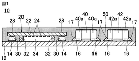
- FIG. 1 It is a sectional view solution figure showing an example of the front end module as a compound module concerning this invention. It is a perspective view which shows the surface acoustic wave element (duplexer) etc. as an electronic component element mounted in the one main surface side of the mounting board
- FIG. 1 shows the state which has arrange
- FIG. 1 is a cross-sectional view showing an example of a front end module as a composite module according to the present invention
- FIG. 2 shows one main surface of a mounting board before forming a molding material in the front end module shown in FIG.
- FIG. 3 is a perspective view showing a surface acoustic wave element (filter) or the like as an electronic component element mounted on the side
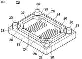
- FIG. 3 is a perspective view showing the surface acoustic wave element used in the front end module shown in FIG.
- the mounting substrate 12 for example, a multilayer substrate such as a ceramic substrate, a printed substrate, or a flexible substrate, or a single layer substrate is used.
- a plurality of mounting electrodes 14 for mounting the surface acoustic wave element 20 as a duplexer or a filter are formed on one main surface of the mounting substrate 12 at intervals.
- the area of each mounting electrode 14 is formed larger than the area of each bump electrode 28 of the surface acoustic wave element 20 described later.
- an inductor 40, a capacitor 42, a first SAW filter 44, a second SAW filter 46, and a switch IC 48 as other surface mount electronic component elements used in the front end module 10 are provided on one main surface of the mounting substrate 12.
- a number of other mounting electrodes 16 for mounting are formed at intervals.
- a surface acoustic wave element 20 is mounted on one main surface side of the mounting substrate 12.
- the surface acoustic wave element 20 includes a piezoelectric substrate 22.
- the piezoelectric substrate 22 is formed of a piezoelectric material such as LiTiO 3 , LiNbO 3 , or sapphire, for example.
- a plurality of comb electrodes 24 are formed on the one main surface of the piezoelectric substrate 22 as a vibration propagation portion at the center thereof.
- the surface acoustic wave element 20 is a SAW filter
- four lead electrodes 26 are formed on one main surface of the piezoelectric substrate 22 from a plurality of comb-tooth electrodes 24 to four corners of the one main surface of the piezoelectric substrate 22, respectively. Is done.
- four circular bump electrodes 28 are formed on one main surface of the piezoelectric substrate 22 at the ends of the four extraction electrodes 26, that is, at four corners of the one main surface of the piezoelectric substrate 22. That is, the comb-tooth electrode 24 and the bump electrode 28 are formed at an interval and are electrically connected.
- These comb-tooth electrodes 24 are made of, for example, Al
- the extraction electrodes 26 and the bump electrodes 28 are made of, for example, Au.
- the bump electrode 30 is formed so that its diameter is smaller than the diameter of the bump electrode 28. Therefore, the plurality of comb-teeth electrodes 24 and the bump electrodes 30 are also formed at an interval and are electrically connected.
- the bump electrode 30 is formed of, for example, solder or Au.
- a frame-shaped dam portion 32 is formed between the comb-tooth electrode 24 and the four bump electrodes 30.
- the dam portion 32 is formed on the inner side of the bump electrode 30 at a distance from the plurality of comb-tooth electrodes 24 and the four bump electrodes 30, and is formed around the comb-tooth electrode 24. It is also formed on the electrode 26. Further, the height of the dam portion 32 from the one main surface of the piezoelectric substrate 22 is formed to be 10 ⁇ m to 150 ⁇ m, for example.
- the dam portion 32 is formed such that the maximum height of the bump electrode 30 from one main surface of the piezoelectric substrate 12 is higher than the maximum height of the dam portion 32 from one main surface of the piezoelectric substrate 12. . Further, the width from the outer peripheral surface to the inner peripheral surface of the dam portion 32 is formed to be 5 ⁇ m to 100 ⁇ m, for example.
- the dam portion 32 is formed of a synthetic resin such as polyimide, polyamideimide, epoxy, or silicone, for example, but may contain a filler such as SiO 2 . Examples of the method of forming the dam portion 32 include spin coating, a method of laminating a semi-cured sheet of the above material, a printing method, and the like. Thereafter, a photolithography process for exposure and development is performed, and the dam portion 32 is processed into a predetermined shape.
- the dam portion 32 is preferably formed of a photosensitive resin material.
- the bump electrode 28 of the surface acoustic wave element 20 mounted on the one main surface side of the mounting substrate 12 is electrically connected to the mounting electrode 14 of the mounting substrate 12 via the melted and solidified bump electrode 30. .
- the dam portion 32 of the surface acoustic wave element 20 is in contact with one main surface of the mounting substrate 12.
- a hollow portion 34 is formed on the comb electrode 24 side of the dam portion 32 and around the comb electrode 24.
- an inductor 40, a capacitor 42, a first SAW filter 44, a second SAW filter 46, and a switch IC 48 are mounted on one main surface side of the mounting substrate 12.
- the two external electrodes 40a of the inductor 40 and the two external electrodes 42a of the capacitor 42, and the external electrodes (not shown) of the first SAW filter 44, the second SAW filter 46, and the switch IC 48 are respectively
- a plurality of other mounting electrodes 16 of the mounting substrate 12 are connected to each other through the solder layer 17.
- a structure having the same structure as that of the surface acoustic wave element 20, for example, a bulk acoustic wave (BAW) filter may be used.
- BAW bulk acoustic wave
- the surface acoustic wave element 20, the inductor 40, the capacitor 42, the first SAW filter 44, the second SAW filter 46, and the switch IC 48 are covered with a molding material 50 made of molding resin.
- the mounting board 12 to be prepared may be a parent board in which a plurality of mounting boards 12 are arranged in the vertical and horizontal directions, or may be a child board made of one mounting board 12.
- each bump electrode 30 of the surface acoustic wave element 20 is formed of solder.
- solder layers 17 are respectively formed on a number of other mounting electrodes 16 on the mounting substrate 12.
- a solder paste may be printed on another mounting electrode 16 and then dispensed or transferred.
- the two external electrodes 40a of the inductor 40, the two external electrodes 42a of the capacitor 42, and the first SAW filter are formed on many other mounting electrodes 16 on which the solder layer 17 is formed. 44, external electrodes (not shown) of the second SAW filter 46 and the switch IC 48 are respectively arranged.
- each external electrode such as two external electrodes 40 a of the inductor 40 and two external electrodes 42 a of the capacitor 42 is replaced with each solder layer 17. And are electrically connected to a number of other mounting electrodes 16 of the mounting substrate 12 respectively.
- the inductor 40, the capacitor 42, the first SAW filter 44, the second SAW filter 46, and the switch IC 48 are mounted on the one main surface side of the mounting substrate 12.
- a flux layer 15 is formed on each mounting electrode 14 of the mounting substrate 12.
- the flux may be printed on the mounting electrode 14, dispensed, or transferred.
- the flux layer 15 on the mounting electrode 14 may be formed by transferring the flux onto each bump electrode 30 of the surface acoustic wave element 20.
- a solder paste may be printed on each mounting electrode 14 and then dispensed or transferred to form a solder layer, or the solder paste may be transferred onto each bump electrode 30 Thus, a solder layer may be formed.
- solder layer and the flux layer so as to be shifted outward from the mounting electrodes 14.
- each bump electrode 30 of the surface acoustic wave element 20 is disposed on each mounting electrode 14 of the mounting substrate 12.
- each bump electrode 28 of the surface acoustic wave element 20 is electrically connected to each mounting electrode 14 of the mounting substrate 12 via each bump electrode 30, and the dam portion 32 of the surface acoustic wave element 20 is connected.
- a hollow portion 34 is brought into contact with one main surface of the mounting substrate 12 and between the piezoelectric substrate 22 of the surface acoustic wave element 20 and the mounting substrate 12 on the comb electrode 24 side of the dam portion 32 and around the comb electrode 24.
- the surface acoustic wave element 20 is mounted on the one main surface side of the mounting substrate 12.
- the surface acoustic wave element 20 may be mounted on one main surface side of the mounting substrate 12 simultaneously with the mounting of the inductor 40, the capacitor 42, the first SAW filter 44, the second SAW filter 46, and the switch IC 48. Good.
- the flux adhering to the mounting substrate 12 and the surface acoustic wave element 20 is cleaned with a cleaning liquid.
- the surface acoustic wave element 20, the inductor 40, the capacitor 42, the first SAW filter 44, the second SAW filter 46, and the switch IC 48 are covered with a molding material 50 made of molding resin.
- a liquid mold resin is applied to the surface acoustic wave element 20 and other surface-mounted electronic component elements, and after removing bubbles below the surface acoustic wave element 20 and other surface-mounted electronic component elements, the mold resin is used. To cure.
- This liquid mold resin is composed of, for example, a SiO 2 filler, an epoxy resin, a curing agent, and the like.
- a solid mold resin, a granule mold resin, or a sheet mold resin may be used.
- the front end module 10 is manufactured.
- the dam portion 32 is formed between the comb electrode 24 and the bump electrode 30 on one main surface side of the piezoelectric substrate 22.
- the solder for the bump electrode 30, the flux, the cleaning liquid for cleaning the flux, the mold resin for molding the surface acoustic wave element 20 and the like with the molding material 50 are blocked by the dam portion 32, and the comb electrode Intrusion into the hollow portion 34 around 24 can be prevented. Therefore, it is possible to prevent the electrical characteristics of the surface acoustic wave element 20 and thus the electrical characteristics of the front end module 10 from being changed by the solder, the flux, and the mold resin.
- the element alone is made of a substrate or resin compared to a surface acoustic wave element in which a hollow portion is formed around the comb-tooth electrode with a substrate or resin in the element alone. Since it is not necessary to form a package structure, it is possible to reduce the size and height. Therefore, the front end module 10 is smaller and lower in height than the front end module using a surface acoustic wave element in which a hollow portion is formed around the comb-teeth electrode with a substrate, resin, or the like in a single element. It is possible to reduce costs and simplify the manufacturing process.
- the dam portion 32 is formed in a frame shape around the comb electrode 24 on the one main surface side of the piezoelectric substrate 22.
- the mold resin for molding the solder, the flux, the surface acoustic wave element 20 and the like is completely blocked by the dam portion 32 and completely prevents the hollow portion 34 around the comb-tooth electrode 24 from entering. be able to.
- the dam portion 32 is formed in a frame shape around the comb electrode 24 on the one main surface side of the piezoelectric substrate 22 in this way, the amount of thermal contraction and thermal expansion by the dam portion 32 around the comb electrode 24.
- the amount can be made uniform, and the stress applied to the portion of the piezoelectric substrate 22 where the comb-tooth electrode 24 is formed and its peripheral portion can also be made uniform. Therefore, warpage and undulation of the piezoelectric substrate 22 can be alleviated, and changes in the electrical characteristics of the surface acoustic wave element 20 due to deformation of the piezoelectric substrate 22 can be suppressed.
- the maximum height of the bump electrode 30 from one main surface of the piezoelectric substrate 22 is the maximum height of the dam portion 32 from one main surface of the piezoelectric substrate 22. Since the surface acoustic wave element 20 is mounted on the mounting substrate 12, when the surface acoustic wave element 20 is disposed so that the bump electrode 30 and the dam portion 32 face the mounting substrate 12, the bump electrode 30 is formed. Reliably contacts the mounting electrode 14 on the mounting substrate 12, so that the surface acoustic wave element 20 can be positioned with high precision.
- the bump electrode 30 of the surface acoustic wave element 20 is mounted on the mounting board when the surface acoustic wave element 20 is disposed on the mounting board 12.
- the surface acoustic wave element 20 is difficult to be placed at an accurate position.
- the dam portion 32 is formed inside the bump electrode 30, and extends from the comb electrode 24 to the bump electrode 28 on one main surface of the piezoelectric substrate 22. Since it is formed on the extracted extraction electrode 26, an extra space for the dam portion 32 is not required outside the bump electrode 30, so that the planar size can be easily reduced.
- the dam portion 32 when the dam portion 32 is formed of a photosensitive resin material, the dam portion 32 can be patterned using photolithography, thereby simplifying the process. it can.
- the surface of the piezoelectric substrate 22 on the surface of one main surface other than the electrically connected portions (the bump electrodes 28 and the bump electrodes 30) is resistant to the surface.
- a solderable protective film is formed, it is possible to prevent the solder from spreading in the electrical connection using the solder.
- the bump electrode 30 and the dam part 32 are formed with a space therebetween, the possibility that one material of the bump electrode 30 and the dam part 32 adheres to the other surface is suppressed.
- the surface acoustic wave element 20 including the bump electrode 30 is covered with the molding material 50 and mechanically connected not only by the bump electrode 30 but also by the molding material 50.
- the mechanical and electrical connection reliability by the electrode 30 is improved.
- the surface acoustic wave device described in Patent Document 1 since the resin does not adhere to the metal bumps, only the mounting substrate and the bumps are connected, and between the mounting substrate and the bumps due to an impact such as heating or dropping after the connection. Problems such as disconnection may occur.
- the surface acoustic wave element 20 including the bump electrode 30 is covered with the molding material 50, so that even if the bump electrode 30 is melted, it leaks to the outside of the molding material 50. There is no.
- the surface acoustic wave element 20 and the like are covered with the molding material 50 made of one type of molding resin, so that the surface acoustic wave element is compared with the case where it is covered with two or more types of resin.
- the stress applied to 20 or the like does not become a complicated mechanism, and the stress applied to the connection portion such as the surface acoustic wave element 20 is easily understood by performing a simulation in advance, and it is easy to take a countermeasure against the stress.
- the bump electrode 30 is melted by solidification by reflow and solidified.
- the electrode 28 is electrically connected to the mounting electrode 14 of the mounting substrate 12 via the bump electrode 30, the bump electrode 30 spreads by the mounting electrode 14 and the height of the bump electrode 30 becomes lower.
- the dam portion 32 of the surface acoustic wave element 20 reliably contacts one main surface of the mounting substrate 12. Therefore, the solder and flux for the bump electrode 30 and the resin for molding the surface acoustic wave element 20 are surely dammed by the dam part 32 and enter the hollow part 34 around the comb-tooth electrode 24. Can be reliably prevented.
- Table 1 shows the results of examining the degree of adhesion between the dam portion 32 and the mounting substrate 12 under the conditions 1 to 4 in which the diameter of the mounting electrode 14 is changed with respect to the diameter of the bump electrode 28.
- the height of the dam portion 32 was 20 ⁇ m
- the diameter of the bump electrode 28 was 80 ⁇ m
- the initial height of the bump electrode 30 was 35 ⁇ m
- the diameter of the mounting electrode 14 was 100 ⁇ m to 200 ⁇ m.
- the height of the bump electrode between the element and the substrate after mounting indicates the bump electrode 30 between the surface acoustic wave element 20 and the mounting substrate 12 after the surface acoustic wave element 20 is mounted on the mounting substrate 12.
- the height indicates a gap between the dam part 32 and the mounting board 12 after the surface acoustic wave element 20 is mounted on the mounting board 12.
- the bump electrode 30 is initially formed on the surface acoustic wave element 20 side.
- the bump electrode 30 is formed on the mounting substrate 12 side.
- the mounting substrate 12 the surface acoustic wave element 20, the inductor 40, the capacitor 42, the first SAW filter 44, the first Two SAW filters 46 and a switch IC 48 are prepared.
- the surface acoustic wave element 20 is prepared as a surface acoustic wave element 20 on which no bump electrode 30 is formed.
- the inductor 40, the capacitor 42, the first SAW filter 44, and the second SAW filter 46 as other surface-mounted electronic component elements are formed on one main surface side of the mounting substrate 12.
- the switch IC 48 is mounted.
- solder is also printed on the mounting electrode 14 on which the surface acoustic wave element 20 is mounted, and the solder printed on the mounting electrode 14 when other surface mount electronic component elements such as the inductor 40 are mounted by reflow.
- the bump electrode 30 is formed on the mounting electrode 14 with solder.
- the bump electrode 28 of the surface acoustic wave element 20 is disposed on the bump electrode 30.
- the bump electrode 28 of the surface acoustic wave element 20 may be disposed on the bump electrode 30 as it is.
- the bump of the surface acoustic wave element 20 is formed.
- the electrode 28 may be disposed on the bump electrode 30.
- the flux layer may be formed on the bump electrode 28 instead of being formed on the bump electrode 30.
- a solder layer may be formed on the bump electrode 30 or the bump electrode 28 by applying solder instead of the flux layer.
- the front end module 10 is manufactured by melting and solidifying the bump electrode 30 in the same manner as in the example of the manufacturing method described above.
- the bump electrode 30 formed of solder is used.
- the bump electrode 30 formed of Au is used. Use.
- the mounting substrate 12 the surface acoustic wave element 20, the inductor 40, the capacitor 42, the first SAW filter 44, the first Two SAW filters 46 and a switch IC 48 are prepared.
- the bump electrode 30 is formed of Au.
- the inductor 40, the capacitor 42, the first SAW filter 44, and the second SAW filter 46 as other surface-mounted electronic component elements are formed on one main surface side of the mounting substrate 12.
- the switch IC 48 is mounted.
- the flux adhering to other surface mount electronic component elements such as the mounting substrate 12 and the inductor 40 is cleaned with a cleaning liquid.
- each bump electrode 30 formed on the surface acoustic wave element 20 is arranged on each mounting electrode 14 of the mounting substrate 12, and on each mounting electrode 14 of the mounting substrate 12 by pressurization, heating, and ultrasonic vibration. Bonding is performed.
- the bonding stage temperature is set to 200 ° C., and a pressure of 230 ° C. and 0.1 MPa is applied for 1 second with a bonding nozzle. In this manner, the surface acoustic wave element 20 is mounted on the one main surface side of the mounting substrate 12.
- the height of the bump electrode 30 is 70 ⁇ m
- the height of the dam portion 32 is 20 ⁇ m
- the height of the bump electrode 30 is increased. Is 15 ⁇ m.
- the dam portion 32 is also pressurized, the height of the dam portion 32 becomes 15 ⁇ m, and the dam portion 32 comes into close contact with the mounting substrate 12, whereby a hollow portion 34 is formed around the comb electrode 24.
- the dam portion 32 includes the comb electrode 24 and the bump. It is not necessary to form between the electrodes 30, and it may be formed outside the bump electrode 30.
- the surface acoustic wave element 20, the inductor 40, the capacitor 42, the first SAW filter 44, and the second SAW filter 46 are provided on one main surface side of the mounting substrate 12. Then, the front-end module 10 is manufactured by covering the switch IC 48 with a molding material 50 made of molding resin.
- FIG. 9 is an illustrative sectional view showing another example of a front end module as a composite module according to the present invention.
- the front end module 10 shown in FIG. 9 has a groove between the portion where the mounting electrode 14 is formed on one main surface of the mounting substrate 12 and the portion where the dam portion 32 contacts. Or the recessed part 18 is formed.
- the concave portion 18 can be formed by a laser when the mounting substrate 12 is made of a ceramic substrate, and can be formed by a half cut by a dicing router or the like when the mounting substrate 12 is made of a printed substrate or a flexible substrate.
- front end module 10 shown in FIG. 9 has the same structure as the front end module 10 shown in FIG. 1, the same effect as the front end module 10 shown in FIG.
- the recess 18 is formed between the part where the mounting electrode 14 is formed on the one main surface of the mounting substrate 12 and the part where the dam part 32 contacts. Therefore, it is possible to prevent the solder and flux for the bump electrode 30 from flowing into the dam portion 32 side.
- the recess 18 may have a continuous groove shape or a structure in which non-through via holes are continuously arranged.
- the manufacturing method of the front end module 10 after mounting another surface mount electronic component element such as the inductor 40 on one main surface side of the mounting substrate 12, flux is applied to the mounting electrodes 14 of the mounting substrate 12.
- the flux layer 15 is formed by coating, but before mounting other surface-mounted electronic component elements such as the inductor 40 on one main surface side of the mounting substrate 12, the flux is mounted on the mounting electrodes 14 of the mounting substrate 12. May be applied to form the flux layer 15. In this way, other surface-mounted electronic component elements such as the inductor 40 do not get in the way, and the flux can be easily applied onto the mounting electrode 14 of the mounting substrate 12.
- the bump electrode 30 and the dam part 32 are formed with a space therebetween, but the bump electrode 30 and the dam part 32 may be formed in contact with each other.
- the surface acoustic wave element 20 described above includes one main surface of the mounting substrate 12 together with the inductor 40, the capacitor 42, the first SAW filter 44, the second SAW filter 46, and the switch IC 48 as other surface-mounted electronic component elements.
- the front end module 10 is configured by being mounted on the side, it may be mounted on a mounting board together with other surface-mounted electronic component elements, or may be mounted on the mounting board itself.
- the surface acoustic wave element has been described as an example of the electronic component element according to the present invention.
- the electronic component element according to the present invention may be a bulk wave element or a MEMS other than the surface acoustic wave element. .
- the composite module according to the present invention is not limited to the front-end module, but may be another composite module equipped with an RF-IC or the like.
- the electronic component element according to the present invention is suitably used for a composite module such as a front-end module using an electronic component element such as a surface acoustic wave element, a bulk wave element, or MEMS.
Landscapes
- Physics & Mathematics (AREA)
- Acoustics & Sound (AREA)
- Surface Acoustic Wave Elements And Circuit Networks Thereof (AREA)
Description
この発明は、電子部品素子、それを用いた複合モジュールおよび複合モジュールの製造方法に関し、特に、圧電基板と圧電基板の一方主面に形成されたインターデジタルトランスデューサ(IDT)ないし櫛歯電極とを有する例えば弾性表面波素子、バルク波素子およびMEMSなどの電子部品素子、それを用いた例えばフロントエンドモジュールなどの複合モジュールおよび複合モジュールの製造方法に関する。
この発明の背景となる従来の弾性表面波装置などの電子部品装置の一例が、例えば特開2003-142972公報(特許文献1参照)に記載されている。特許文献1に記載されている電子部品装置としての弾性表面波装置では、圧電基板上にインターデジタルトランスデューサ(IDT)ないし櫛歯電極が形成された弾性表面波素子が、櫛歯電極を形成した面を配線基板ないし実装基板側に向けて実装されている。この場合、この弾性表面波装置では、弾性表面波素子が金属バンプを介して実装基板側に電気的に接続され、金属バンプとともに弾性表面波素子が第1樹脂および第2樹脂で被覆されている。また、この場合、この弾性表面波装置では、第1樹脂などによって、弾性表面波素子の櫛歯電極の周囲に中空部が形成される。
特許文献1に記載されている弾性表面波装置では、弾性表面波素子を実装基板に実装する際に、金属バンプのためのはんだやフラックスが弾性表面波素子の櫛歯電極の周囲の中空部に侵入する可能性がある。
さらに、特許文献1に記載されている弾性表面波装置では、弾性表面波素子などを被覆する樹脂として粘性の高い樹脂を使用しても、弾性表面波素子などを樹脂で被覆する際に、樹脂が弾性表面波素子の櫛歯電極の周囲の中空部に侵入する可能性がある。
上述のように、はんだやフラックスまたは樹脂が弾性表面波素子の櫛歯電極の周囲の中空部に侵入すると、弾性表面波素子の電気特性が変化してしまう場合がある。
さらに、特許文献1に記載されている弾性表面波装置では、弾性表面波素子などを被覆する樹脂として粘性の高い樹脂を使用しても、弾性表面波素子などを樹脂で被覆する際に、樹脂が弾性表面波素子の櫛歯電極の周囲の中空部に侵入する可能性がある。
上述のように、はんだやフラックスまたは樹脂が弾性表面波素子の櫛歯電極の周囲の中空部に侵入すると、弾性表面波素子の電気特性が変化してしまう場合がある。
それゆえに、この発明の主たる目的は、実装時および実装後にはんだやフラックスなどが櫛歯電極の周囲に侵入しにくい弾性表面波素子などの電子部品素子、それを用いた複合モジュールおよび複合モジュールの製造方法を提供することである。
この発明にかかる電子部品素子は、圧電基板と、圧電基板の一方主面に形成された櫛歯電極と、圧電基板の一方主面において櫛歯電極と間隔を隔てて形成されかつ櫛歯電極に電気的に接続されたバンプ用電極と、圧電基板の一方主面側においてバンプ用電極上に形成されたバンプ電極と、圧電基板の一方主面側において櫛歯電極およびバンプ電極間に形成されたダム部とを含む、電子部品素子である。
この発明にかかる電子部品素子では、ダム部は、圧電基板の一方主面側において櫛歯電極の周囲に枠状に形成されていることが好ましい。
また、この発明にかかる電子部品素子では、圧電基板の一方主面からのバンプ電極の最大の高さは、圧電基板の一方主面からのダム部の最大の高さより高く形成されていることが好ましい。
さらに、この発明にかかる電子部品素子では、ダム部は、バンプ電極より内側に形成され、かつ、圧電基板の一方主面において櫛歯電極からバンプ用電極にわたって引き出された引出し電極上に形成されていることが好ましい。
また、この発明にかかる電子部品素子では、ダム部は、感光性の樹脂材料で形成されていることが好ましい。
さらに、この発明にかかる電子部品素子では、圧電基板の一方主面側において、電気的に接続される部分以外の部分の表面に耐はんだ性の保護膜が形成されていることが好ましい。
この発明にかかる電子部品素子は、例えば、弾性表面波素子、バルク波素子またはMEMSなどである。
この発明にかかる複合モジュールは、一方主面に実装用電極が形成された実装基板と、実装基板の一方主面側に実装されたこの発明にかかる電子部品素子と、電子部品素子を被覆するモールド樹脂からなるモールド材とを含み、電子部品素子のバンプ用電極は、バンプ電極を介して実装基板の実装用電極に電気的に接続され、電子部品素子のダム部は、実装基板の一方主面に接触し、さらに電子部品素子の圧電基板および実装基板間において電子部品素子のダム部より櫛歯電極側であって電子部品素子の櫛歯電極の周囲に中空部が形成された、複合モジュールである。
この発明にかかる複合モジュールでは、実装基板の一方主面において、実装用電極が形成された部分およびダム部が接触する部分間に凹部が形成されていることが好ましい。
また、この発明にかかる複合モジュールでは、実装用電極の面積は、バンプ用電極の面積より大きく形成されていることが好ましい。
この発明にかかる複合モジュールの製造方法は、この発明にかかる複合モジュールを製造するための複合モジュールの製造方法であって、一方主面に実装用電極が形成された実装基板を準備する工程と、この発明にかかる電子部品素子を準備する工程と、実装基板の実装用電極上または電子部品素子のバンプ電極上に、フラックス層またははんだ層を形成する工程と、電子部品素子のバンプ電極を実装基板の実装用電極上に配置する工程と、バンプ電極を溶融して固化することによって、電子部品素子のバンプ用電極をバンプ電極を介して実装基板の実装用電極に電気的に接続し、電子部品素子のダム部を実装基板の一方主面に接触するとともに、電子部品素子の圧電基板および実装基板間において電子部品素子のダム部より櫛歯電極側であって電子部品素子の櫛歯電極の周囲に中空部を形成する工程と、電子部品素子をモールド樹脂からなるモールド材で被覆する工程とを含む、複合モジュールの製造方法である。
また、この発明にかかる複合モジュールの製造方法は、この発明にかかる複合モジュールを製造するための複合モジュールの製造方法であって、一方主面に実装用電極が形成された実装基板を準備する工程と、この発明にかかる電子部品素子であってバンプ電極が形成されていない電子部品素子を準備する工程と、実装基板の実装用電極上にバンプ電極を形成する工程と、バンプ電極上または電子部品素子のバンプ用電極上に、フラックス層またははんだ層を形成する工程と、電子部品素子のバンプ用電極をバンプ電極上に配置する工程と、バンプ電極を溶融して固化することによって、電子部品素子のバンプ用電極をバンプ電極を介して実装基板の実装用電極に電気的に接続し、電子部品素子のダム部を実装基板の一方主面に接触するとともに、電子部品素子の圧電基板および実装基板間において電子部品素子のダム部より櫛歯電極側であって電子部品素子の櫛歯電極の周囲に中空部を形成する工程と、電子部品素子をモールド樹脂からなるモールド材で被覆する工程とを含む、複合モジュールの製造方法である。
この発明にかかる複合モジュールの製造方法は、例えば、実装基板において電子部品素子が電気的に接続される実装用電極以外の他の実装用電極上にはんだ層を形成する工程と、はんだ層を形成した他の実装用電極上に他の表面実装電子部品素子の外部電極を配置する工程と、他の実装用電極上のはんだ層を溶融して固化することによって、他の表面実装電子部品素子の外部電極を他の実装用電極上のはんだ層を介して実装基板の他の実装用電極に電気的に接続する工程とを含み、モールド材で被覆する工程は、電子部品素子および他の表面実装電子部品素子をモールド樹脂からなるモールド材で被覆する。
この発明にかかる電子部品素子では、ダム部は、圧電基板の一方主面側において櫛歯電極の周囲に枠状に形成されていることが好ましい。
また、この発明にかかる電子部品素子では、圧電基板の一方主面からのバンプ電極の最大の高さは、圧電基板の一方主面からのダム部の最大の高さより高く形成されていることが好ましい。
さらに、この発明にかかる電子部品素子では、ダム部は、バンプ電極より内側に形成され、かつ、圧電基板の一方主面において櫛歯電極からバンプ用電極にわたって引き出された引出し電極上に形成されていることが好ましい。
また、この発明にかかる電子部品素子では、ダム部は、感光性の樹脂材料で形成されていることが好ましい。
さらに、この発明にかかる電子部品素子では、圧電基板の一方主面側において、電気的に接続される部分以外の部分の表面に耐はんだ性の保護膜が形成されていることが好ましい。
この発明にかかる電子部品素子は、例えば、弾性表面波素子、バルク波素子またはMEMSなどである。
この発明にかかる複合モジュールは、一方主面に実装用電極が形成された実装基板と、実装基板の一方主面側に実装されたこの発明にかかる電子部品素子と、電子部品素子を被覆するモールド樹脂からなるモールド材とを含み、電子部品素子のバンプ用電極は、バンプ電極を介して実装基板の実装用電極に電気的に接続され、電子部品素子のダム部は、実装基板の一方主面に接触し、さらに電子部品素子の圧電基板および実装基板間において電子部品素子のダム部より櫛歯電極側であって電子部品素子の櫛歯電極の周囲に中空部が形成された、複合モジュールである。
この発明にかかる複合モジュールでは、実装基板の一方主面において、実装用電極が形成された部分およびダム部が接触する部分間に凹部が形成されていることが好ましい。
また、この発明にかかる複合モジュールでは、実装用電極の面積は、バンプ用電極の面積より大きく形成されていることが好ましい。
この発明にかかる複合モジュールの製造方法は、この発明にかかる複合モジュールを製造するための複合モジュールの製造方法であって、一方主面に実装用電極が形成された実装基板を準備する工程と、この発明にかかる電子部品素子を準備する工程と、実装基板の実装用電極上または電子部品素子のバンプ電極上に、フラックス層またははんだ層を形成する工程と、電子部品素子のバンプ電極を実装基板の実装用電極上に配置する工程と、バンプ電極を溶融して固化することによって、電子部品素子のバンプ用電極をバンプ電極を介して実装基板の実装用電極に電気的に接続し、電子部品素子のダム部を実装基板の一方主面に接触するとともに、電子部品素子の圧電基板および実装基板間において電子部品素子のダム部より櫛歯電極側であって電子部品素子の櫛歯電極の周囲に中空部を形成する工程と、電子部品素子をモールド樹脂からなるモールド材で被覆する工程とを含む、複合モジュールの製造方法である。
また、この発明にかかる複合モジュールの製造方法は、この発明にかかる複合モジュールを製造するための複合モジュールの製造方法であって、一方主面に実装用電極が形成された実装基板を準備する工程と、この発明にかかる電子部品素子であってバンプ電極が形成されていない電子部品素子を準備する工程と、実装基板の実装用電極上にバンプ電極を形成する工程と、バンプ電極上または電子部品素子のバンプ用電極上に、フラックス層またははんだ層を形成する工程と、電子部品素子のバンプ用電極をバンプ電極上に配置する工程と、バンプ電極を溶融して固化することによって、電子部品素子のバンプ用電極をバンプ電極を介して実装基板の実装用電極に電気的に接続し、電子部品素子のダム部を実装基板の一方主面に接触するとともに、電子部品素子の圧電基板および実装基板間において電子部品素子のダム部より櫛歯電極側であって電子部品素子の櫛歯電極の周囲に中空部を形成する工程と、電子部品素子をモールド樹脂からなるモールド材で被覆する工程とを含む、複合モジュールの製造方法である。
この発明にかかる複合モジュールの製造方法は、例えば、実装基板において電子部品素子が電気的に接続される実装用電極以外の他の実装用電極上にはんだ層を形成する工程と、はんだ層を形成した他の実装用電極上に他の表面実装電子部品素子の外部電極を配置する工程と、他の実装用電極上のはんだ層を溶融して固化することによって、他の表面実装電子部品素子の外部電極を他の実装用電極上のはんだ層を介して実装基板の他の実装用電極に電気的に接続する工程とを含み、モールド材で被覆する工程は、電子部品素子および他の表面実装電子部品素子をモールド樹脂からなるモールド材で被覆する。
この発明にかかる電子部品素子では、圧電基板の一方主面側において櫛歯電極およびバンプ電極間にダム部が形成されているので、実装時および実装後に、バンプ電極のためのはんだやフラックスおよび電子部品素子をモールドするための樹脂などが、ダム部によって堰き止められ、櫛歯電極の周囲に侵入することを防止することができる。そのため、そのようなはんだやフラックスおよび樹脂によって、弾性表面波素子の電気特性が変化することを防止することができる。
さらに、この発明にかかる電子部品素子では、素子単体において基板や樹脂などで櫛歯電極の周囲に中空部を形成した電子部品素子と比べて、素子単体において基板や樹脂が不要となるので、小型化および低背化が可能となる。
この発明にかかる電子部品素子では、ダム部が圧電基板の一方主面側において櫛歯電極の周囲に枠状に形成された場合、バンプ電極のためのはんだやフラックスおよび電子部品素子をモールドするための樹脂などが、ダム部によって完全に堰き止められ、櫛歯電極の周囲に侵入することを完全に防止することができる。このようにダム部が圧電基板の一方主面側において櫛歯電極の周囲に枠状に形成されると、櫛歯電極の周囲においてダム部による熱収縮量・熱膨張量を均一化することができ、圧電基板において櫛歯電極が形成された部分およびその周辺部分に加わる応力も均一化することができるため、圧電基板の反りやうねりを緩和することができ、圧電基板の変形による電子部品素子の電気特性の変化を抑えることができる。
また、この発明にかかる電子部品素子では、圧電基板の一方主面からのバンプ電極の最大の高さが圧電基板の一方主面からのダム部の最大の高さより高く形成された場合、電子部品素子を実装基板に実装する際、バンプ電極およびダム部が実装基板に向くように電子部品素子を配置した場合、バンプ電極が実装基板上の実装用電極に確実に接触するため、電子部品素子の実装時に位置決めを精度よく行うことができる。なお、ダム部の最大の高さがバンプ電極の最大の高いより高い場合、電子部品素子を実装基板上に配置する際に、電子部品素子のバンプ電極が実装基板の実装用電極上に浮いた形になり、電子部品素子を正確な位置に配置しにくい。
さらに、この発明にかかる電子部品素子では、ダム部が、バンプ電極より内側に形成され、かつ、圧電基板の一方主面において櫛歯電極からバンプ用電極にわたって引き出された引出し電極上に形成された場合、バンプ電極より外側においてダム部のための余分なスペースが不要となるので、平面的なサイズの小型化が容易になる。
また、この発明にかかる電子部品素子では、ダム部が感光性の樹脂材料で形成された場合、フォトリソグラフィーを用いたダム部のパターニングが可能となり、プロセスの簡略化ができる。
さらに、この発明にかかる電子部品素子では、圧電基板の一方主面側において、電気的に接続される部分以外の部分の表面に耐はんだ性の保護膜が形成された場合、はんだを用いた電気的な接続において、はんだの濡れ広がりを保護膜によって防止することができる。
この発明にかかる複合モジュールでは、この発明にかかる電子部品素子が用いられているので、バンプ電極のためのはんだやフラックスおよび電子部品素子をモールドするための樹脂などが、ダム部によって堰き止められ、櫛歯電極の周囲に侵入することを防止することができ、そのようなはんだやフラックスおよび樹脂によって、電子部品素子の電気特性が変化することを防止することができる。
また、この発明にかかる複合モジュールでは、バンプ電極を含む電子部品素子がモールド材で被覆され、バンプ電極だけでなくモールド材によっても機械的に接続されることになるので、バンプ電極による機械的および電気的な接続信頼性が向上する。
さらに、この発明にかかる複合モジュールでは、この発明にかかる電子部品素子が用いられているので、素子単体において基板や樹脂などで櫛歯電極の周囲に中空部を形成した電子部品素子が用いられた複合モジュールと比べて、小型化および低背化が可能となる。
この発明にかかる複合モジュールでは、実装基板の一方主面において、実装用電極が形成された部分およびダム部が接触する部分間に凹部が形成された場合、凹部によって、バンプ電極のためのはんだやフラックスがダム部側に流入することを防止することができる。
また、この発明にかかる複合モジュールでは、実装用電極の面積がバンプ用電極の面積より大きく形成された場合、バンプ電極を溶融して固化することによって電子部品素子のバンプ用電極をバンプ電極を介して実装基板の実装用電極に電気的に接続する際、バンプ電極が実装用電極により広がってバンプ電極の高さがより低くなるので、電子部品素子のダム部が実装基板の一方主面に確実に接触する。そのため、バンプ電極のためのはんだやフラックスおよび電子部品素子をモールドするための樹脂などが、ダム部によって確実に堰き止められ、櫛歯電極の周囲に侵入することを確実に防止することができる。
この発明にかかる複合モジュールの製造方法によれば、この発明にかかる複合モジュールを製造することができる。
また、この発明にかかる複合モジュールの製造方法では、実装基板の一方主面側に電子部品素子および他の表面実装電子部品素子が実装され、電子部品素子および他の表面実装電子部品素子がモールド材で被覆された複合モジュールも製造することができる。
さらに、この発明にかかる電子部品素子では、素子単体において基板や樹脂などで櫛歯電極の周囲に中空部を形成した電子部品素子と比べて、素子単体において基板や樹脂が不要となるので、小型化および低背化が可能となる。
この発明にかかる電子部品素子では、ダム部が圧電基板の一方主面側において櫛歯電極の周囲に枠状に形成された場合、バンプ電極のためのはんだやフラックスおよび電子部品素子をモールドするための樹脂などが、ダム部によって完全に堰き止められ、櫛歯電極の周囲に侵入することを完全に防止することができる。このようにダム部が圧電基板の一方主面側において櫛歯電極の周囲に枠状に形成されると、櫛歯電極の周囲においてダム部による熱収縮量・熱膨張量を均一化することができ、圧電基板において櫛歯電極が形成された部分およびその周辺部分に加わる応力も均一化することができるため、圧電基板の反りやうねりを緩和することができ、圧電基板の変形による電子部品素子の電気特性の変化を抑えることができる。
また、この発明にかかる電子部品素子では、圧電基板の一方主面からのバンプ電極の最大の高さが圧電基板の一方主面からのダム部の最大の高さより高く形成された場合、電子部品素子を実装基板に実装する際、バンプ電極およびダム部が実装基板に向くように電子部品素子を配置した場合、バンプ電極が実装基板上の実装用電極に確実に接触するため、電子部品素子の実装時に位置決めを精度よく行うことができる。なお、ダム部の最大の高さがバンプ電極の最大の高いより高い場合、電子部品素子を実装基板上に配置する際に、電子部品素子のバンプ電極が実装基板の実装用電極上に浮いた形になり、電子部品素子を正確な位置に配置しにくい。
さらに、この発明にかかる電子部品素子では、ダム部が、バンプ電極より内側に形成され、かつ、圧電基板の一方主面において櫛歯電極からバンプ用電極にわたって引き出された引出し電極上に形成された場合、バンプ電極より外側においてダム部のための余分なスペースが不要となるので、平面的なサイズの小型化が容易になる。
また、この発明にかかる電子部品素子では、ダム部が感光性の樹脂材料で形成された場合、フォトリソグラフィーを用いたダム部のパターニングが可能となり、プロセスの簡略化ができる。
さらに、この発明にかかる電子部品素子では、圧電基板の一方主面側において、電気的に接続される部分以外の部分の表面に耐はんだ性の保護膜が形成された場合、はんだを用いた電気的な接続において、はんだの濡れ広がりを保護膜によって防止することができる。
この発明にかかる複合モジュールでは、この発明にかかる電子部品素子が用いられているので、バンプ電極のためのはんだやフラックスおよび電子部品素子をモールドするための樹脂などが、ダム部によって堰き止められ、櫛歯電極の周囲に侵入することを防止することができ、そのようなはんだやフラックスおよび樹脂によって、電子部品素子の電気特性が変化することを防止することができる。
また、この発明にかかる複合モジュールでは、バンプ電極を含む電子部品素子がモールド材で被覆され、バンプ電極だけでなくモールド材によっても機械的に接続されることになるので、バンプ電極による機械的および電気的な接続信頼性が向上する。
さらに、この発明にかかる複合モジュールでは、この発明にかかる電子部品素子が用いられているので、素子単体において基板や樹脂などで櫛歯電極の周囲に中空部を形成した電子部品素子が用いられた複合モジュールと比べて、小型化および低背化が可能となる。
この発明にかかる複合モジュールでは、実装基板の一方主面において、実装用電極が形成された部分およびダム部が接触する部分間に凹部が形成された場合、凹部によって、バンプ電極のためのはんだやフラックスがダム部側に流入することを防止することができる。
また、この発明にかかる複合モジュールでは、実装用電極の面積がバンプ用電極の面積より大きく形成された場合、バンプ電極を溶融して固化することによって電子部品素子のバンプ用電極をバンプ電極を介して実装基板の実装用電極に電気的に接続する際、バンプ電極が実装用電極により広がってバンプ電極の高さがより低くなるので、電子部品素子のダム部が実装基板の一方主面に確実に接触する。そのため、バンプ電極のためのはんだやフラックスおよび電子部品素子をモールドするための樹脂などが、ダム部によって確実に堰き止められ、櫛歯電極の周囲に侵入することを確実に防止することができる。
この発明にかかる複合モジュールの製造方法によれば、この発明にかかる複合モジュールを製造することができる。
また、この発明にかかる複合モジュールの製造方法では、実装基板の一方主面側に電子部品素子および他の表面実装電子部品素子が実装され、電子部品素子および他の表面実装電子部品素子がモールド材で被覆された複合モジュールも製造することができる。
この発明によれば、実装時および実装後にはんだやフラックスなどが櫛歯電極の周囲に侵入しにくい弾性表面波素子などの電子部品素子、それを用いた複合モジュールおよび複合モジュールの製造方法が得られる。
この発明の上述の目的、その他の目的、特徴および利点は、図面を参照して行う以下の発明を実施するための形態の説明から一層明らかとなろう。
図1は、この発明にかかる複合モジュールとしてのフロントエンドモジュールの一例を示す断面図解図であり、図2は、図1に示すフロントエンドモジュールにおいてモールド材を形成する前の実装基板の一方主面側に実装された電子部品素子としての弾性表面波素子(フィルタ)などを示す斜視図であり、図3は、図1に示すフロントエンドモジュールに用いられる弾性表面波素子を示す斜視図である。
図1に示すフロントエンドモジュール10は、実装基板12を含む。実装基板12としては、例えば、セラミック基板、プリント基板、フレキシブル基板などの多層基板や単層基板が用いられる。
実装基板12の一方主面には、デュプレクサまたはフィルタとしての弾性表面波素子20を実装するための複数の実装用電極14が間隔を隔てて形成される。なお、各実装用電極14の面積は、後述の弾性表面波素子20の各バンプ用電極28の面積より大きく形成されている。さらに、実装基板12の一方主面には、フロントエンドモジュール10に用いられる他の表面実装電子部品素子としてのインダクタ40、キャバシタ42、第1のSAWフィルタ44、第2のSAWフィルタ46およびスイッチIC48を実装するための多数の他の実装用電極16が間隔を隔てて形成される。
実装基板12の一方主面側には、弾性表面波素子20が実装される。この弾性表面波素子20は、圧電基板22を含む。圧電基板22は、例えば、LiTiO3、LiNbO3、サファイア等の圧電体で形成される。
圧電基板22の一方主面には、その中央に、振動伝搬部として複数の櫛歯電極24が形成される。また、弾性表面波素子20がSAWフィルタの場合、圧電基板22の一方主面には、複数の櫛歯電極24から圧電基板22の一方主面の4隅にわたって、4つの引出し電極26がそれぞれ形成される。さらに、圧電基板22の一方主面には、4つの引出し電極26の端部に、すなわち圧電基板22の一方主面の4隅に、例えば円形の4つのバンプ用電極28がそれぞれ形成される。すなわち、櫛歯電極24とバンプ用電極28とは、間隔を隔てて形成され、かつ、電気的に接続される。これらの櫛歯電極24は例えばAl、引出し電極26およびバンプ用電極28は例えばAuでそれぞれ形成される。
圧電基板22の一方主面側において、4つのバンプ用電極28上には、例えば円柱状の4つのバンプ電極30がそれぞれ形成される。バンプ電極30は、その直径がバンプ用電極28の直径より小さくなるように形成される。したがって、複数の櫛歯電極24とバンプ電極30とも、間隔を隔てて形成され、かつ、電気的に接続される。また、バンプ電極30は、例えばはんだまたはAuで形成される。
圧電基板22の一方主面側において、櫛歯電極24および4つのバンプ電極30間には、例えば枠状のダム部32が形成される。この場合、ダム部32は、複数の櫛歯電極24および4つのバンプ電極30から間隔を隔てて、バンプ電極30より内側に形成され、かつ、櫛歯電極24の周囲に形成され、4つの引出し電極26上にも形成される。また、圧電基板22の一方主面からのダム部32の高さは、例えば10μm~150μmに形成される。この場合、ダム部32は、圧電基板12の一方主面からのバンプ電極30の最大の高さが圧電基板12の一方主面からのダム部32の最大の高さより高くなるように形成される。さらに、ダム部32の外周面から内周面までの幅は、例えば5μm~100μmに形成される。ダム部32は、例えば、ポリイミド、ポリアミドイミド、エポキシ、シリコーン等の合成樹脂で形成されるが、SiO2等のフィラーが含有されいてもよい。ダム部32の形成方法としては、スピンコート、上記材料の半硬化シートをラミネートする方法、印刷法等が挙げられ、その後、露光・現像を行うフォトリソプロセスを行い、所定の形状に加工される。また、ダム部32は、感光性の樹脂材料で形成されることが好ましい。
実装基板12の一方主面側に実装された弾性表面波素子20のバンプ用電極28は、溶融し固化したバンプ電極30を介して、実装基板12の実装用電極14に電気的に接続される。また、弾性表面波素子20のダム部32は、実装基板12の一方主面に接触する。さらに、弾性表面波素子20の圧電基板22および実装基板12間において、ダム部32より櫛歯電極24側であって櫛歯電極24の周囲に、中空部34が形成される。
さらに、実装基板12の一方主面側には、インダクタ40、キャバシタ42、第1のSAWフィルタ44、第2のSAWフィルタ46およびスイッチIC48が実装される。この場合、インダクタ40の2つの外部電極40aおよびキャパシタ42の2つの外部電極42aや、第1のSAWフィルタ44、第2のSAWフィルタ46およびスイッチIC48の各外部電極(図示せず)が、各はんだ層17を介して、実装基板12の多数の他の実装電極16にそれぞれ接続される。なお、第1のSAWフィルタ44および第2のSAWフィルタ46としては、それぞれ、弾性表面波素子20と同様の構造のもの、例えばバルク弾性波(BAW)フィルタなどが用いられてもよい。
さらに、弾性表面波素子20、インダクタ40、キャパシタ42、第1のSAWフィルタ44、第2のSAWフィルタ46およびスイッチIC48は、モールド樹脂からなるモールド材50で被覆される。
次に、上述のフロントエンドモジュール10の製造方法の一例について説明する。
まず、上述の実装用電極14および他の実装用電極16が形成された実装基板12を準備する。この場合、準備する実装基板12としては、複数の実装基板12が縦横に配列された親基板であってもよく、または、1つの実装基板12からなる子基板であってもよい。
さらに、上述の弾性表面波素子20、インダクタ40、キャパシタ42、第1のSAWフィルタ44、第2のSAWフィルタ46およびスイッチIC48を準備する。この場合、弾性表面波素子20の各バンプ電極30をはんだで形成する。
そして、図4に示すように、実装基板12の多数の他の実装用電極16上にはんだ層17をそれぞれ形成する。このようにはんだ層17を形成するためには、例えば、他の実装用電極16上にはんだペーストを印刷し、ディスペンスしまたは転写すればよい。
それから、図5に示すように、はんだ層17を形成した多数の他の実装用電極16上に、インダクタ40の2つの外部電極40aおよびキャパシタ42の2つの外部電極42aや、第1のSAWフィルタ44、第2のSAWフィルタ46およびスイッチIC48の各外部電極(図示せず)をそれぞれ配置する。
そして、図6に示すように、各はんだ層17を溶融して固化することによって、インダクタ40の2つの外部電極40aおよびキャパシタ42の2つの外部電極42aなど各外部電極を、各はんだ層17を介して、実装基板12の多数の他の実装用電極16にそれぞれ電気的に接続する。
このようにして、インダクタ40、キャパシタ42、第1のSAWフィルタ44、第2のSAWフィルタ46およびスイッチIC48を実装基板12の一方主面側に実装する。
さらに、図6に示すように、実装基板12の各実装用電極14上にフラックス層15をそれぞれ形成する。このようにフラックス層15を形成するためには、例えば、実装用電極14上にフラックスを印刷し、ディスペンスしまたは転写すればよい。
なお、実装用電極14上にフラックス層15を形成する代わりに、弾性表面波素子20の各バンプ電極30上にフラックスを転写してフラックス層を形成してもよい。あるいは、フラックス層を形成する代わりに、各実装用電極14上にはんだペーストを印刷し、ディスペンスしまたは転写してはんだ層を形成してもよく、または、各バンプ電極30上にはんだペーストを転写してはんだ層を形成してもよい。
また、はんだやフラックスをダム部32の内部に流入させないようにするために、はんだ層やフラックス層を各実装用電極14よりも外側にずらして形成することが望ましい。
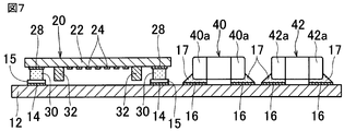
そして、図7に示すように、弾性表面波素子20の各バンプ電極30を、実装基板12の各実装用電極14上にそれぞれ配置する。
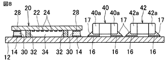
それから、図8に示すように、バンプ電極30をリフローで溶融して固化する。それによって、弾性表面波素子20の各バンプ用電極28を、各バンプ電極30を介して、実装基板12の各実装用電極14に電気的に接続し、弾性表面波素子20のダム部32を実装基板12の一方主面に接触するとともに、弾性表面波素子20の圧電基板22および実装基板12間においてダム部32より櫛歯電極24側であって櫛歯電極24の周囲に中空部34を形成する。
このようにして、弾性表面波素子20を実装基板12の一方主面側に実装する。
なお、実装基板12の一方主面側には、インダクタ40、キャパシタ42、第1のSAWフィルタ44、第2のSAWフィルタ46およびスイッチIC48の実装と同時に、弾性表面波素子20を実装してもよい。
そして、実装基板12や弾性表面波素子20などに付着しているフラックスを洗浄液で洗浄する。
それから、実装基板12の一方主面側において、弾性表面波素子20、インダクタ40、キャパシタ42、第1のSAWフィルタ44、第2のSAWフィルタ46およびスイッチIC48をモールド樹脂からなるモールド材50で被覆する。この場合、弾性表面波素子20や他の表面実装電子部品素子に例えば液状のモールド樹脂を塗布し、弾性表面波素子20や他の表面実装電子部品素子の下部の気泡を除去した後に、モールド樹脂を硬化する。この液状のモールド樹脂は、例えば、SiO2フィラー、エポキシ樹脂、硬化剤等で構成される。なお、液状のモールド樹脂の代わりに、固形状のモールド樹脂、顆粒状のモールド樹脂、シート状のモールド樹脂を用いてもよい。
ここで、圧電基板12として親基板を用いて加工を行った場合には、ダイシングなどにより個片化して、個々のフロントエンドモジュール10とする。
このようにして、フロントエンドモジュール10を製造する。
上述のフロントエンドモジュール10に用いられる弾性表面波素子20では、圧電基板22の一方主面側において櫛歯電極24およびバンプ電極30間にダム部32が形成されているので、実装時および実装後に、バンプ電極30のためのはんだやフラックス、フラックスを洗浄するための洗浄液および弾性表面波素子20などをモールド材50でモールドするためのモールド樹脂などが、ダム部32によって堰き止められ、櫛歯電極24の周囲の中空部34に侵入することを防止することができる。そのため、はんだやフラックスおよびモールド樹脂によって、弾性表面波素子20の電気特性ひいてはフロントエンドモジュール10の電気特性が変化することを防止することができる。
さらに、フロントエンドモジュール10に用いられる弾性表面波素子20では、素子単体において基板や樹脂などで櫛歯電極の周囲に中空部を形成した弾性表面波素子と比べて、素子単体において基板や樹脂でパッケージ構造を形成することが不要となるので、小型化および低背化が可能となる。そのため、このフロントエンドモジュール10では、素子単体において基板や樹脂などで櫛歯電極の周囲に中空部を形成した弾性表面波素子が用いられたフロントエンドモジュールと比べて、小型化および低背化が可能となるとともに、コスト削減や製造プロセスの簡略化ができる。
また、フロントエンドモジュール10に用いられる弾性表面波素子20では、ダム部32が圧電基板22の一方主面側において櫛歯電極24の周囲に枠状に形成されているので、バンプ電極30のためのはんだやフラックスおよび弾性表面波素子20などをモールドするためのモールド樹脂などが、ダム部32によって完全に堰き止められ、櫛歯電極24の周囲の中空部34に侵入することを完全に防止することができる。また、このようにダム部32が圧電基板22の一方主面側において櫛歯電極24の周囲に枠状に形成されるので、櫛歯電極24の周囲においてダム部32による熱収縮量・熱膨張量を均一化することができ、圧電基板22において櫛歯電極24が形成された部分およびその周辺部分に加わる応力も均一化することができる。そのため、圧電基板22の反りやうねりを緩和することができ、圧電基板22の変形による弾性表面波素子20の電気特性の変化を抑えることができる。
さらに、フロントエンドモジュール10に用いられる弾性表面波素子20では、圧電基板22の一方主面からのバンプ電極30の最大の高さが圧電基板22の一方主面からのダム部32の最大の高さより高く形成されているので、弾性表面波素子20を実装基板12に実装する際、バンプ電極30およびダム部32が実装基板12に向くように弾性表面波素子20を配置した場合、バンプ電極30が実装基板12上の実装用電極14に確実に接触するため、弾性表面波素子20の実装時に位置決めを精度よく行うことができる。なお、ダム部32の最大の高さがバンプ電極30の最大の高いより高い場合、弾性表面波素子20を実装基板12上に配置する際に、弾性表面波素子20のバンプ電極30が実装基板12の実装用電極14上に浮いた形になり、弾性表面波素子20を正確な位置に配置しにくい。
また、フロントエンドモジュール10に用いられる弾性表面波素子20では、ダム部32が、バンプ電極30より内側に形成され、かつ、圧電基板22の一方主面において櫛歯電極24からバンプ用電極28にわたって引き出された引出し電極26上に形成されているので、バンプ電極30より外側においてダム部32のための余分なスペースが不要となるので、平面的なサイズの小型化が容易になる。
さらに、フロントエンドモジュール10に用いられる弾性表面波素子20では、ダム部32が感光性の樹脂材料で形成された場合、フォトリソグラフィーを用いたダム部32のパターニングが可能となり、プロセスの簡略化ができる。
また、フロントエンドモジュール10に用いられる弾性表面波素子20では、圧電基板22の一方主面側において、電気的に接続される部分(バンプ用電極28およびバンプ電極30)以外の部分の表面に耐はんだ性の保護膜を形成した場合、はんだを用いた電気的な接続において、はんだの濡れ広がりを保護膜によって防止することができる。
さらに、上述のフロントエンドモジュール10では、バンプ電極30およびダム部32が間隔を隔てて形成されているので、バンプ電極30およびダム部32の一方の材料が他方の表面に付着する可能性を抑えることができ、特に、バンプ電極30の表面にダム部32の材料である合成樹脂が付着して電気的な接続不良が発生する可能性を抑えることができる。
また、このフロントエンドモジュール10では、バンプ電極30を含む弾性表面波素子20がモールド材50で被覆され、バンプ電極30だけでなくモールド材50によっても機械的に接続されることになるので、バンプ電極30による機械的および電気的な接続信頼性が向上する。なお、特許文献1に記載されている弾性表面波装置では、金属バンプに樹脂が付着しないため、実装基板とバンプだけの接続となり、接続後の加熱や落下などの衝撃により実装基板およびバンプ間で断線などの不具合が発生する可能性がある。
さらに、このフロントエンドモジュール10では、バンプ電極30を含む弾性表面波素子20などがモールド材50で被覆されているので、バンプ電極30などがたとえ溶融したとしても、モールド材50の外部に漏れることはない。
また、このフロントエンドモジュール10では、弾性表面波素子20などが1種類のモールド樹脂からなるモールド材50で被覆されているので、2種類以上の樹脂で被覆する場合に比べて、弾性表面波素子20などに加わる応力が複雑なメカニズムとならなく、事前にシミュレーションすることで弾性表面波素子20などの接続部分に加わる応力が分かりやすく、応力対策を立てやすい。
さらに、このフロントエンドモジュール10では、実装用電極14の面積がバンプ用電極28の面積より大きく形成されているので、バンプ電極30をリフローで溶融して固化することによって弾性表面波素子20のバンプ用電極28をバンプ電極30を介して実装基板12の実装用電極14に電気的に接続する際、バンプ電極30が実装用電極14により広がってバンプ電極30の高さがより低くなるので、弾性表面波素子20のダム部32が実装基板12の一方主面に確実に接触する。そのため、バンプ電極30のためのはんだやフラックスおよび弾性表面波素子20をモールドするための樹脂などが、ダム部32によって確実に堰き止められ、櫛歯電極24の周囲の中空部34に侵入することを確実に防止することができる。
ここで、バンプ用電極28の直径に対して実装用電極14の直径を変化した条件1~4の場合のダム部32および実装基板12の密着度合いを調べた結果を表1に示す。なお、ダム部32の高さを20μmとし、バンプ用電極28の直径を80μmとし、バンプ電極30の初期の高さを35μmとし、実装用電極14の直径を100μm~200μmとした。

表1において、「実装後の素子-基板間のバンプ電極の高さ」は、弾性表面波素子20を実装基板12に実装した後の弾性表面波素子20および実装基板12間におけるバンプ電極30の高さを示し、「実装後のダム部-基板間のギャップ」は、弾性表面波素子20を実装基板12に実装した後のダム部32および実装基板12間のギャップを示す。
表1に示す結果より、弾性表面波素子20のバンプ用電極28の直径に対して、実装基板12の実装用電極14の直径を大きくすることによって、弾性表面波素子20のリフロー時の沈み込み量が異なり、弾性表面波素子20に形成しているダム部32と実装基板12との密着度合いが変化する。
さらに、表1に示す結果より、実装基板12の実装用電極14の直径を150μm以上にすることによって、弾性表面波素子20の沈み込み量が増し、ダム部32および実装基板12間のギャップがゼロとなり、ダム部32と実装基板12とが密着し、櫛歯電極24の周囲に中空部24を形成することが可能となる。
さらに、表1に示す結果より、実装基板12の実装用電極14の直径を150μm以上にすることによって、弾性表面波素子20の沈み込み量が増し、ダム部32および実装基板12間のギャップがゼロとなり、ダム部32と実装基板12とが密着し、櫛歯電極24の周囲に中空部24を形成することが可能となる。
また、上述のリフロー後に、例えば4インチ角の親基板(実装基板12)上に搭載された弾性表面波素子20上に100gの重石を載せて0.001N/mm2の圧力を加えて、再度リフローした結果を表2に示す。なお、ここでは、弾性表面波素子20が親基板上の4インチ角(約100mm×100mm)の面積の1/10の面積で実装されているとして、弾性表面波素子20上に0.001N/mm2の圧力が加えられるとしている。

表2に示す結果より、実装用電極14が小さいものでもダム部32と実装基板12とが密着し、櫛歯電極24の周囲に中空部34を形成することが可能となる。
次に、上述のフロントエンドモジュール10の製造方法の他の例について説明する。
上述のフロントエンドモジュール10の製造方法の一例では、初期的にバンプ電極30を弾性表面波素子20側に形成しているが、このフロントエンドモジュール10の製造方法の他の例では、初期的にバンプ電極30を実装基板12側に形成する。
このフロントエンドモジュール10の製造方法の他の例では、まず、上述の製造方法の一例と同様に、実装基板12、弾性表面波素子20、インダクタ40、キャパシタ42、第1のSAWフィルタ44、第2のSAWフィルタ46およびスイッチIC48を準備する。ただし、弾性表面波素子20は、バンプ電極30が形成されていない弾性表面波素子20を準備する。
そして、上述の製造方法の一例と同様に、実装基板12の一方主面側に、他の表面実装電子部品素子としてのインダクタ40、キャパシタ42、第1のSAWフィルタ44、第2のSAWフィルタ46およびスイッチIC48を実装する。
この場合、弾性表面波素子20を実装する実装用電極14にもはんだを印刷し、インダクタ40などの他の表面実装電子部品素子をリフローで実装する際に、実装用電極14上に印刷したはんだも溶融し、実装用電極14上にはんだでバンプ電極30を形成する。
この場合、弾性表面波素子20を実装する実装用電極14にもはんだを印刷し、インダクタ40などの他の表面実装電子部品素子をリフローで実装する際に、実装用電極14上に印刷したはんだも溶融し、実装用電極14上にはんだでバンプ電極30を形成する。
それから、バンプ電極30上に、弾性表面波素子20のバンプ用電極28を配置する。この場合、そのまま弾性表面波素子20のバンプ用電極28をバンプ電極30上に配置してもよいが、バンプ電極30上にフラックスを塗布してフラックス層を形成した後に弾性表面波素子20のバンプ用電極28をバンプ電極30上に配置してもよい。また、フラックス層をバンプ電極30上に形成する代わりにバンプ用電極28上に形成してもよい。あるいは、バンプ電極30上にまたはバンプ用電極28上には、フラックス層の代わりに、はんだを塗布してはんだ層を形成してもよい。
そして、以降は、上述の製造方法の一例と同様に、バンプ電極30を溶融して固化するなどして、フロントエンドモジュール10を製造する。
次に、上述のフロントエンドモジュール10の製造方法の別の例について説明する。上述のフロントエンドモジュール10の製造方法の一例では、はんだで形成されたバンプ電極30を用いているが、このフロントエンドモジュール10の製造方法の別の例では、Auで形成されたバンプ電極30を用いる。
このフロントエンドモジュール10の製造方法の別の例では、まず、上述の製造方法の一例と同様に、実装基板12、弾性表面波素子20、インダクタ40、キャパシタ42、第1のSAWフィルタ44、第2のSAWフィルタ46およびスイッチIC48を準備する。ただし、バンプ電極30をAuで形成する。
そして、上述の製造方法の一例と同様に、実装基板12の一方主面側に、他の表面実装電子部品素子としてのインダクタ40、キャパシタ42、第1のSAWフィルタ44、第2のSAWフィルタ46およびスイッチIC48を実装する。
それから、実装基板12やインダクタ40などの他の表面実装電子部品素子に付着しているフラックスを洗浄液で洗浄する。
そして、弾性表面波素子20に形成した各バンプ電極30を、実装基板12の各実装用電極14上に配置し、加圧・加熱・超音波振動により、実装基板12の各実装用電極14上にボンディングを行う。
この場合、例えば、ボンディングステージ温度を200℃とし、ボンディングノズルで230℃、0.1MPaの加圧を1秒間加える。
このようにして、弾性表面波素子20を実装基板12の一方主面側に実装する。
ここで、初期的には、バンプ電極30の高さが70μmであり、ダム部32の高さが20μmであり、弾性表面波素子20の実装基板12への実装後には、バンプ電極30の高さが15μmとなる。しかしながら、ダム部32も加圧され、ダム部32の高さが15μmとなり、ダム部32が実装基板12に密着することで櫛歯電極24の周囲に中空部34が形成される。
この場合、例えば、ボンディングステージ温度を200℃とし、ボンディングノズルで230℃、0.1MPaの加圧を1秒間加える。
このようにして、弾性表面波素子20を実装基板12の一方主面側に実装する。
ここで、初期的には、バンプ電極30の高さが70μmであり、ダム部32の高さが20μmであり、弾性表面波素子20の実装基板12への実装後には、バンプ電極30の高さが15μmとなる。しかしながら、ダム部32も加圧され、ダム部32の高さが15μmとなり、ダム部32が実装基板12に密着することで櫛歯電極24の周囲に中空部34が形成される。
なお、このようにAuで形成されたバンプ電極30を用いる場合、櫛歯電極24の周囲の中空部34へのフラックスの流入の懸念がないために、ダム部32は、櫛歯電極24およびバンプ電極30間に形成される必要はなく、バンプ電極30の外側に形成されてもよい。
そして、以降は、上述の製造方法の一例と同様に、実装基板12の一方主面側において、弾性表面波素子20、インダクタ40、キャパシタ42、第1のSAWフィルタ44、第2のSAWフィルタ46およびスイッチIC48をモールド樹脂からなるモールド材50で被覆して、フロントエンドモジュール10を製造する。
図9は、この発明にかかる複合モジュールとしてのフロントエンドモジュールの他の例を示す断面図解図である。
図9に示すフロントエンドモジュール10は、図1に示すフロントエンドモジュール10と比べて、実装基板12の一方主面において実装用電極14が形成された部分およびダム部32が接触する部分間に溝ないし凹部18が形成されている。この凹部18は、実装基板12がセラミック基板からなる場合にはレーザで形成することができ、プリント基板やフレキシブル基板からなる場合にはダイシングルータなどによるハーフカットで形成することができる。
図9に示すフロントエンドモジュール10では、図1に示すフロントエンドモジュール10と同様の構造を有するので、図1に示すフロントエンドモジュール10と同様の効果を奏する。
さらに、図9に示すフロントエンドモジュール10では、実装基板12の一方主面において実装用電極14が形成された部分およびダム部32が接触する部分間に凹部18が形成されているので、凹部18によって、バンプ電極30のためのはんだやフラックスがダム部32側に流入することを防止することができる。なお、凹部18は連続した溝状でもよいし、非貫通ビアホールが連続的に配置された構造などでもよい。
上述のフロントエンドモジュール10の製造方法の一例では、実装基板12の一方主面側にインダクタ40などの他の表面実装電子部品素子を実装した後に、実装基板12の実装用電極14上にフラックスを塗布してフラックス層15を形成しているが、実装基板12の一方主面側にインダクタ40などの他の表面実装電子部品素子を実装する前に、実装基板12の実装用電極14上にフラックスを塗布してフラックス層15を形成してもよい。このようにすれば、インダクタ40などの他の表面実装電子部品素子が邪魔にならず、実装基板12の実装用電極14上にフラックスを塗布しやすい。
また、上述のフロントエンドモジュール10では、バンプ電極30およびダム部32が間隔を隔てて形成されているが、バンプ電極30およびダム部32は接触して形成されてもよい。
さらに、上述の弾性表面波素子20は、他の表面実装電子部品素子としてインダクタ40、キャパシタ42、第1のSAWフィルタ44、第2のSAWフィルタ46およびスイッチIC48とともに、実装基板12の一方主面側に実装されることによって、フロントエンドモジュール10を構成しているが、その他の表面実装電子部品素子とともに実装基板に実装されてもよく、または、それ自体が実装基板に実装されてもよい。
また、この発明にかかる電子部品素子として弾性表面波素子を例にして説明したが、この発明にかかる電子部品素子としては、弾性表面波素子以外に例えばバルク波素子またはMEMSなどであってもよい。
さらに、この発明にかかる複合モジュールとしても、フロントエンドモジュールに限らず、RF-ICなどを備えた他の複合モジュールであってもよい。
この発明にかかる電子部品素子は、特に例えば、弾性表面波素子、バルク波素子、MEMSなどの電子部品素子を用いたフロントエンドモジュールなどの複合モジュールに好適に用いられる。
10 フロントエンドモジュール
12 実装基板
14 実装用電極
15 フラックス層
16 他の実装用電極
17 はんだ層
18 凹部
20 弾性表面波素子
22 圧電基板
24 櫛歯電極
26 引出し電極
28 バンプ用電極
30 バンプ電極
32 ダム部
34 中空部
40 インダクタ
40a 外部電極
42 キャパシタ
42a 外部電極
44 第1のSAWフィルタ
46 第2のSAWフィルタ
48 スイッチIC
50 モールド材
12 実装基板
14 実装用電極
15 フラックス層
16 他の実装用電極
17 はんだ層
18 凹部
20 弾性表面波素子
22 圧電基板
24 櫛歯電極
26 引出し電極
28 バンプ用電極
30 バンプ電極
32 ダム部
34 中空部
40 インダクタ
40a 外部電極
42 キャパシタ
42a 外部電極
44 第1のSAWフィルタ
46 第2のSAWフィルタ
48 スイッチIC
50 モールド材
Claims (15)
- 圧電基板、
前記圧電基板の一方主面に形成された櫛歯電極、
前記圧電基板の一方主面において前記櫛歯電極と間隔を隔てて形成されかつ前記櫛歯電極に電気的に接続されたバンプ用電極、
前記圧電基板の一方主面側において前記バンプ用電極上に形成されたバンプ電極、および
前記圧電基板の一方主面側において前記櫛歯電極および前記バンプ電極間に形成されたダム部を含む、電子部品素子。 - 前記ダム部は、前記圧電基板の一方主面側において前記櫛歯電極の周囲に枠状に形成された、請求項1に記載の電子部品素子。
- 前記圧電基板の一方主面からの前記バンプ電極の最大の高さは、前記圧電基板の一方主面からの前記ダム部の最大の高さより高く形成された、請求項1または請求項2に記載の電子部品素子。
- 前記ダム部は、前記バンプ電極より内側に形成され、かつ、前記圧電基板の一方主面において前記櫛歯電極から前記バンプ用電極にわたって引き出された引出し電極上に形成された、請求項1ないし請求項3のいずれかに記載の電子部品素子。
- 前記ダム部は、感光性の樹脂材料で形成された、請求項1ないし請求項4のいずれかに記載の電子部品素子。
- 前記圧電基板の一方主面側において、電気的に接続される部分以外の部分の表面に耐はんだ性の保護膜が形成された、請求項1ないし請求項5のいずれかに記載の電子部品素子。
- 前記電子部品素子は、弾性表面波素子である、請求項1ないし請求項6のいずれかに記載の電子部品素子。
- 前記電子部品素子は、バルク波素子である、請求項1ないし請求項6のいずれかに記載の電子部品素子。
- 前記電子部品素子は、MEMSである、請求項1ないし請求項6のいずれかに記載の電子部品素子。
- 一方主面に実装用電極が形成された実装基板、
前記実装基板の一方主面側に実装された請求項1ないし請求項9のいずれかに記載の電子部品素子、および
前記電子部品素子を被覆するモールド樹脂からなるモールド材を含み、
前記電子部品素子の前記バンプ用電極は、前記バンプ電極を介して前記実装基板の前記実装用電極に電気的に接続され、
前記電子部品素子の前記ダム部は、前記実装基板の一方主面に接触し、さらに
前記電子部品素子の前記圧電基板および前記実装基板間において前記電子部品素子の前記ダム部より前記櫛歯電極側であって前記電子部品素子の前記櫛歯電極の周囲に中空部が形成された、複合モジュール。 - 前記実装基板の一方主面において、前記実装用電極が形成された部分および前記ダム部が接触する部分間に凹部が形成された、請求項10に記載の複合モジュール。
- 前記実装用電極の面積は、前記バンプ用電極の面積より大きく形成された、請求項10または請求項11に記載の複合モジュール。
- 請求項10に記載の複合モジュールを製造するための複合モジュールの製造方法であって、
一方主面に実装用電極が形成された実装基板を準備する工程、
請求項1ないし請求項9のいずれかに記載の電子部品素子を準備する工程、
前記実装基板の前記実装用電極上または前記電子部品素子の前記バンプ電極上に、フラックス層またははんだ層を形成する工程、
前記電子部品素子の前記バンプ電極を前記実装基板の前記実装用電極上に配置する工程、
前記バンプ電極を溶融して固化することによって、前記電子部品素子の前記バンプ用電極を前記バンプ電極を介して前記実装基板の前記実装用電極に電気的に接続し、前記電子部品素子の前記ダム部を前記実装基板の一方主面に接触するとともに、前記電子部品素子の前記圧電基板および前記実装基板間において前記電子部品素子の前記ダム部より前記櫛歯電極側であって前記電子部品素子の前記櫛歯電極の周囲に中空部を形成する工程、および
前記電子部品素子をモールド樹脂からなるモールド材で被覆する工程を含む、複合モジュールの製造方法。 - 請求項10に記載の複合モジュールを製造するための複合モジュールの製造方法であって、
一方主面に実装用電極が形成された実装基板を準備する工程、
請求項1ないし請求項9のいずれかに記載の電子部品素子であってバンプ電極が形成されていない電子部品素子を準備する工程、
前記実装基板の前記実装用電極上にバンプ電極を形成する工程、
前記バンプ電極上または前記電子部品素子の前記バンプ用電極上に、フラックス層またははんだ層を形成する工程、
前記電子部品素子の前記バンプ用電極を前記バンプ電極上に配置する工程、
前記バンプ電極を溶融して固化することによって、前記電子部品素子の前記バンプ用電極を前記バンプ電極を介して前記実装基板の前記実装用電極に電気的に接続し、前記電子部品素子の前記ダム部を前記実装基板の一方主面に接触するとともに、前記電子部品素子の前記圧電基板および前記実装基板間において前記電子部品素子の前記ダム部より前記櫛歯電極側であって前記電子部品素子の前記櫛歯電極の周囲に中空部を形成する工程、および
前記電子部品素子をモールド樹脂からなるモールド材で被覆する工程を含む、複合モジュールの製造方法。 - 前記実装基板において前記電子部品素子が電気的に接続される実装用電極以外の他の実装用電極上にはんだ層を形成する工程、
前記はんだ層を形成した前記他の実装用電極上に他の表面実装電子部品素子の外部電極を配置する工程、および
前記他の実装用電極上の前記はんだ層を溶融して固化することによって、前記他の表面実装電子部品素子の前記外部電極を前記他の実装用電極上の前記はんだ層を介して前記実装基板の前記他の実装用電極に電気的に接続する工程を含み、
前記モールド材で被覆する工程は、前記電子部品素子および前記他の表面実装電子部品素子をモールド樹脂からなるモールド材で被覆する、請求項13または請求項14に記載の複合モジュールの製造方法。
Applications Claiming Priority (2)
| Application Number | Priority Date | Filing Date | Title |
|---|---|---|---|
| JP2012-044590 | 2012-02-29 | ||
| JP2012044590 | 2012-02-29 |
Publications (1)
| Publication Number | Publication Date |
|---|---|
| WO2013129175A1 true WO2013129175A1 (ja) | 2013-09-06 |
Family
ID=49082375
Family Applications (1)
| Application Number | Title | Priority Date | Filing Date |
|---|---|---|---|
| PCT/JP2013/053940 Ceased WO2013129175A1 (ja) | 2012-02-29 | 2013-02-19 | 電子部品素子、それを用いた複合モジュールおよび複合モジュールの製造方法 |
Country Status (1)
| Country | Link |
|---|---|
| WO (1) | WO2013129175A1 (ja) |
Cited By (7)
| Publication number | Priority date | Publication date | Assignee | Title |
|---|---|---|---|---|
| US20120181898A1 (en) * | 2011-01-19 | 2012-07-19 | Taiyo Yuden Co., Ltd. | Acoustic wave device |
| JP2017199969A (ja) * | 2016-04-25 | 2017-11-02 | 株式会社村田製作所 | 回路モジュール |
| CN109004083A (zh) * | 2018-08-10 | 2018-12-14 | 付伟 | 带有单围堰及焊锡的芯片封装结构及其制作方法 |
| CN109037427A (zh) * | 2018-08-10 | 2018-12-18 | 付伟 | 带有单围堰的芯片封装结构及其制作方法 |
| CN109037428A (zh) * | 2018-08-10 | 2018-12-18 | 付伟 | 带有双围堰的芯片封装结构及其制作方法 |
| CN109065701A (zh) * | 2018-08-10 | 2018-12-21 | 付伟 | 带有单围堰、金属柱及焊锡的芯片封装结构及其制作方法 |
| CN113541628A (zh) * | 2021-06-28 | 2021-10-22 | 杭州左蓝微电子技术有限公司 | 一种声表面波器件及其制造方法 |
Citations (5)
| Publication number | Priority date | Publication date | Assignee | Title |
|---|---|---|---|---|
| JPH0555303A (ja) * | 1991-08-29 | 1993-03-05 | Toshiba Corp | 電子部品装置 |
| JP2003188514A (ja) * | 2001-12-21 | 2003-07-04 | Murata Mfg Co Ltd | 混載型電子回路装置の製造方法 |
| JP2004147028A (ja) * | 2002-10-23 | 2004-05-20 | Toyo Commun Equip Co Ltd | Sawチップ及び表面実装型sawデバイスの製造方法 |
| JP2008252351A (ja) * | 2007-03-29 | 2008-10-16 | Murata Mfg Co Ltd | 弾性表面波素子及びその製造方法 |
| JP2009033333A (ja) * | 2007-07-25 | 2009-02-12 | Nippon Dempa Kogyo Co Ltd | 圧電部品 |
-
2013
- 2013-02-19 WO PCT/JP2013/053940 patent/WO2013129175A1/ja not_active Ceased
Patent Citations (5)
| Publication number | Priority date | Publication date | Assignee | Title |
|---|---|---|---|---|
| JPH0555303A (ja) * | 1991-08-29 | 1993-03-05 | Toshiba Corp | 電子部品装置 |
| JP2003188514A (ja) * | 2001-12-21 | 2003-07-04 | Murata Mfg Co Ltd | 混載型電子回路装置の製造方法 |
| JP2004147028A (ja) * | 2002-10-23 | 2004-05-20 | Toyo Commun Equip Co Ltd | Sawチップ及び表面実装型sawデバイスの製造方法 |
| JP2008252351A (ja) * | 2007-03-29 | 2008-10-16 | Murata Mfg Co Ltd | 弾性表面波素子及びその製造方法 |
| JP2009033333A (ja) * | 2007-07-25 | 2009-02-12 | Nippon Dempa Kogyo Co Ltd | 圧電部品 |
Cited By (12)
| Publication number | Priority date | Publication date | Assignee | Title |
|---|---|---|---|---|
| US20120181898A1 (en) * | 2011-01-19 | 2012-07-19 | Taiyo Yuden Co., Ltd. | Acoustic wave device |
| US8749114B2 (en) * | 2011-01-19 | 2014-06-10 | Taiyo Yuden Co., Ltd. | Acoustic wave device |
| JP2017199969A (ja) * | 2016-04-25 | 2017-11-02 | 株式会社村田製作所 | 回路モジュール |
| US10861900B2 (en) | 2016-04-25 | 2020-12-08 | Murata Manufacturing Co., Ltd. | Circuit module |
| CN109004083A (zh) * | 2018-08-10 | 2018-12-14 | 付伟 | 带有单围堰及焊锡的芯片封装结构及其制作方法 |
| CN109037427A (zh) * | 2018-08-10 | 2018-12-18 | 付伟 | 带有单围堰的芯片封装结构及其制作方法 |
| CN109037428A (zh) * | 2018-08-10 | 2018-12-18 | 付伟 | 带有双围堰的芯片封装结构及其制作方法 |
| CN109065701A (zh) * | 2018-08-10 | 2018-12-21 | 付伟 | 带有单围堰、金属柱及焊锡的芯片封装结构及其制作方法 |
| CN109065701B (zh) * | 2018-08-10 | 2024-03-29 | 浙江熔城半导体有限公司 | 带有单围堰、金属柱及焊锡的芯片封装结构及其制作方法 |
| CN109037427B (zh) * | 2018-08-10 | 2024-07-23 | 浙江熔城半导体有限公司 | 带有单围堰的芯片封装结构及其制作方法 |
| CN109004083B (zh) * | 2018-08-10 | 2024-08-09 | 浙江熔城半导体有限公司 | 带有单围堰及焊锡的芯片封装结构及其制作方法 |
| CN113541628A (zh) * | 2021-06-28 | 2021-10-22 | 杭州左蓝微电子技术有限公司 | 一种声表面波器件及其制造方法 |
Similar Documents
| Publication | Publication Date | Title |
|---|---|---|
| WO2013129175A1 (ja) | 電子部品素子、それを用いた複合モジュールおよび複合モジュールの製造方法 | |
| CN107546135B (zh) | 电子部件装置、电子部件装置向电路基板的安装方法及安装构造 | |
| CN106688180B (zh) | 压电元件及其制造方法 | |
| US7486160B2 (en) | Electronic component and manufacturing method thereof | |
| JP5907195B2 (ja) | 電子部品及び電子部品の製造方法 | |
| JP5755434B2 (ja) | 弾性波装置およびその製造方法 | |
| US10312880B2 (en) | Method for manufacturing electronic component module | |
| KR20110054710A (ko) | 소자 패키지 및 그 제조 방법 | |
| US10812042B2 (en) | Electronic component | |
| KR20180055369A (ko) | 표면탄성파 소자 패키지 및 그 제작 방법 | |
| JP2013225749A (ja) | 圧電デバイス及びモジュール部品 | |
| CN107706118A (zh) | 一种芯片封装方法及芯片封装结构 | |
| US9293684B2 (en) | Electronic part comprising acoustic wave device | |
| JP5880683B2 (ja) | 電子部品素子およびそれを備えた複合モジュール | |
| JP5837845B2 (ja) | 電子部品の製造方法及び電子部品 | |
| JP7416920B2 (ja) | 電子部品、電子デバイス及び電子部品の製造方法 | |
| JP2017157739A (ja) | 電子部品付き配線板の製造方法 | |
| JP5782129B2 (ja) | 電子装置 | |
| US20200343152A1 (en) | Electronic component package and method for manufacturing the same | |
| CN113597669B (zh) | 电子部件及其制造方法 | |
| JP5756715B2 (ja) | 圧電デバイスの製造方法及び圧電デバイス | |
| KR100843419B1 (ko) | 반도체 칩 패키지 및 제조방법 | |
| JP4731216B2 (ja) | 弾性表面波装置 | |
| JP2013051518A (ja) | 圧電デバイス | |
| JP2011009482A (ja) | 部品内蔵基板装置の製造方法 |
Legal Events
| Date | Code | Title | Description |
|---|---|---|---|
| 121 | Ep: the epo has been informed by wipo that ep was designated in this application |
Ref document number: 13754618 Country of ref document: EP Kind code of ref document: A1 |
|
| NENP | Non-entry into the national phase |
Ref country code: DE |
|
| 122 | Ep: pct application non-entry in european phase |
Ref document number: 13754618 Country of ref document: EP Kind code of ref document: A1 |
|
| NENP | Non-entry into the national phase |
Ref country code: JP |