WO2013129147A1 - 走査電子顕微鏡 - Google Patents
走査電子顕微鏡 Download PDFInfo
- Publication number
- WO2013129147A1 WO2013129147A1 PCT/JP2013/053786 JP2013053786W WO2013129147A1 WO 2013129147 A1 WO2013129147 A1 WO 2013129147A1 JP 2013053786 W JP2013053786 W JP 2013053786W WO 2013129147 A1 WO2013129147 A1 WO 2013129147A1
- Authority
- WO
- WIPO (PCT)
- Prior art keywords
- detector
- electrons
- deflector
- electron beam
- electron
- Prior art date
- Legal status (The legal status is an assumption and is not a legal conclusion. Google has not performed a legal analysis and makes no representation as to the accuracy of the status listed.)
- Ceased
Links
Images


Classifications
-
- H—ELECTRICITY
- H01—ELECTRIC ELEMENTS
- H01J—ELECTRIC DISCHARGE TUBES OR DISCHARGE LAMPS
- H01J37/00—Discharge tubes with provision for introducing objects or material to be exposed to the discharge, e.g. for the purpose of examination or processing thereof
- H01J37/02—Details
- H01J37/04—Arrangements of electrodes and associated parts for generating or controlling the discharge, e.g. electron-optical arrangement or ion-optical arrangement
- H01J37/147—Arrangements for directing or deflecting the discharge along a desired path
-
- H—ELECTRICITY
- H01—ELECTRIC ELEMENTS
- H01J—ELECTRIC DISCHARGE TUBES OR DISCHARGE LAMPS
- H01J37/00—Discharge tubes with provision for introducing objects or material to be exposed to the discharge, e.g. for the purpose of examination or processing thereof
- H01J37/02—Details
- H01J37/244—Detectors; Associated components or circuits therefor
-
- H—ELECTRICITY
- H01—ELECTRIC ELEMENTS
- H01J—ELECTRIC DISCHARGE TUBES OR DISCHARGE LAMPS
- H01J37/00—Discharge tubes with provision for introducing objects or material to be exposed to the discharge, e.g. for the purpose of examination or processing thereof
- H01J37/26—Electron or ion microscopes; Electron or ion diffraction tubes
- H01J37/28—Electron or ion microscopes; Electron or ion diffraction tubes with scanning beams
-
- H—ELECTRICITY
- H01—ELECTRIC ELEMENTS
- H01J—ELECTRIC DISCHARGE TUBES OR DISCHARGE LAMPS
- H01J37/00—Discharge tubes with provision for introducing objects or material to be exposed to the discharge, e.g. for the purpose of examination or processing thereof
- H01J37/26—Electron or ion microscopes; Electron or ion diffraction tubes
- H01J37/29—Reflection microscopes
-
- H—ELECTRICITY
- H01—ELECTRIC ELEMENTS
- H01J—ELECTRIC DISCHARGE TUBES OR DISCHARGE LAMPS
- H01J2237/00—Discharge tubes exposing object to beam, e.g. for analysis treatment, etching, imaging
- H01J2237/05—Arrangements for energy or mass analysis
- H01J2237/057—Energy or mass filtering
-
- H—ELECTRICITY
- H01—ELECTRIC ELEMENTS
- H01J—ELECTRIC DISCHARGE TUBES OR DISCHARGE LAMPS
- H01J2237/00—Discharge tubes exposing object to beam, e.g. for analysis treatment, etching, imaging
- H01J2237/06—Sources
- H01J2237/063—Electron sources
-
- H—ELECTRICITY
- H01—ELECTRIC ELEMENTS
- H01J—ELECTRIC DISCHARGE TUBES OR DISCHARGE LAMPS
- H01J2237/00—Discharge tubes exposing object to beam, e.g. for analysis treatment, etching, imaging
- H01J2237/15—Means for deflecting or directing discharge
-
- H—ELECTRICITY
- H01—ELECTRIC ELEMENTS
- H01J—ELECTRIC DISCHARGE TUBES OR DISCHARGE LAMPS
- H01J2237/00—Discharge tubes exposing object to beam, e.g. for analysis treatment, etching, imaging
- H01J2237/15—Means for deflecting or directing discharge
- H01J2237/1501—Beam alignment means or procedures
-
- H—ELECTRICITY
- H01—ELECTRIC ELEMENTS
- H01J—ELECTRIC DISCHARGE TUBES OR DISCHARGE LAMPS
- H01J2237/00—Discharge tubes exposing object to beam, e.g. for analysis treatment, etching, imaging
- H01J2237/244—Detection characterized by the detecting means
- H01J2237/2449—Detector devices with moving charges in electric or magnetic fields
-
- H—ELECTRICITY
- H01—ELECTRIC ELEMENTS
- H01J—ELECTRIC DISCHARGE TUBES OR DISCHARGE LAMPS
- H01J2237/00—Discharge tubes exposing object to beam, e.g. for analysis treatment, etching, imaging
- H01J2237/244—Detection characterized by the detecting means
- H01J2237/24495—Signal processing, e.g. mixing of two or more signals
-
- H—ELECTRICITY
- H01—ELECTRIC ELEMENTS
- H01J—ELECTRIC DISCHARGE TUBES OR DISCHARGE LAMPS
- H01J2237/00—Discharge tubes exposing object to beam, e.g. for analysis treatment, etching, imaging
- H01J2237/26—Electron or ion microscopes
- H01J2237/28—Scanning microscopes
- H01J2237/2813—Scanning microscopes characterised by the application
- H01J2237/2814—Measurement of surface topography
Definitions
- the present invention relates to a scanning electron microscope that detects electrons obtained by irradiating a sample with an electron beam, and more particularly to a scanning electron microscope including a deflector that deflects the trajectory of electrons emitted from the sample.
- Patent Document 1 discloses a technique for speeding up visual field movement using an image shift deflector. Further, in accordance with an electric field or a magnetic field generated in association with an image shift in order to guide electrons to a conversion electrode arranged outside the axis of the electron beam and closer to the electron source than the detector or to the detector. Controlling the deflection angle of secondary electrons is described.
- a scanning electron microscope comprising an electron source, a deflector for deflecting an irradiation position of an electron beam emitted from the electron source, and a control device for controlling the deflector
- the electron A detector for detecting electrons obtained by irradiation of the beam with the sample, an aperture forming member disposed between the detector and the deflector and having a passage aperture for the electron beam, and emitted from the sample
- a secondary signal deflector for deflecting electrons deflects the electrons emitted from the sample toward a passage aperture of the electron beam according to deflection control of the deflector.
- a scanning electron microscope for controlling the next signal deflector is proposed.
- an image is formed by scanning primary electrons on a sample and detecting secondary electrons emitted from the surface of the sample.
- edge contrast decreases due to the diffusion of primary electrons inside the sample, so SEM observation is expected to become even more severe.
- the emitted secondary electrons disappear upon re-collision with the sample side wall, making it difficult to see the shape of the bottom. Therefore, it is conceivable to install an electrode that generates positive electric charge on the sample surface or generates an electric field for guiding electrons upward.
- an electrode that generates positive electric charge on the sample surface or generates an electric field for guiding electrons upward.
- the sample surface is a conductor or the pattern bottom is an insulator
- a method of selectively detecting only the secondary electrons emitted from the bottom of the pattern and emphasizing them is effective in that the apparatus has a function of discriminating secondary electrons by energy or angle.
- an energy filter it is possible to emphasize a specific pattern contrast by using a difference in potential potential of materials. This technique is effective when a plurality of different materials such as Low-k materials and metal gates are used.
- a specific pattern contrast can be enhanced by discriminating secondary electrons by elevation angle or azimuth angle.
- discriminating in the elevation direction it is possible to obtain information on the pattern bottom and side surfaces by selectively detecting secondary electrons emitted in the direction perpendicular to the sample surface.
- An energy filter is generally configured using a plurality of conductive meshes or electrodes.
- the energy resolution is determined by the flatness and electric field strength of the formed electric field, the entrance angle of secondary electrons, orbital dispersion, and the like. If there is a variation in the energy resolution at the time of image acquisition, the potential for cutting the energy changes, resulting in variations in image contrast and brightness.
- a shield for limiting the secondary electron trajectory is generally placed, and for example, only secondary electrons that have passed through a hole or the like opened in the shield are selectively detected. At this time, for example, when secondary electrons in the vertical direction of the sample are to be selectively detected, if the corresponding secondary electron trajectory hits the shield, the effect of angle discrimination cannot be obtained.
- the electron beam is deflected by an image shift deflector or the like, not only the electron beam but also the trajectories of secondary electrons and backscattered electrons may be bent, making it difficult to perform proper angle discrimination.
- the angle discrimination opening and the electron beam passage opening are used together, and a deflector for deflecting the electron emitted from the sample to the opening and the electron passing through the opening, or
- a scanning electron microscope will be described in which a detector for detecting the electrons caused by the electrons is provided, thereby minimizing accurate angle discrimination and collision of electrons with a shield other than the shield for angle discrimination.
- the path with the least possibility of colliding with the electron beam path or the members constituting the electron optical system is an electron beam passage orbit. Therefore, regardless of the deflection of the image shift deflector or the like, the electrons emitted from the sample are deflected so as to pass along the passage opening of the electron beam. It is possible to suppress the collision of the maximum.
- the opening forming member provided with the opening for angle discrimination is an electron detector or a conversion electrode for collision electrons
- the detection surface of the detector or the conversion electrode surface provided in an axial symmetry with respect to the electron beam is used. Since the largest number of electrons can be guided, the detection efficiency can be maximized.
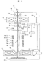
- FIG. 1 is a schematic configuration diagram of a scanning electron microscope.
- the primary electron beam 1 is extracted by applying an extraction voltage 12 between the field emission cathode 11 and the extraction electrode 13.
- the primary electron beam 1 is subjected to a converging action by the condenser lens 14 and subjected to scanning deflection by the upper scanning deflector 21 and the lower scanning deflector 22.
- the deflection intensities of the upper scanning deflector 21 and the lower scanning deflector 22 are adjusted so that the sample 23 is two-dimensionally scanned with the lens center of the objective lens 17 as a fulcrum. Similarly, it receives a deflection action by the upper image shift deflector 25 and the lower image shift deflector 26 for changing the scanning position.
- the deflected primary electron beam 1 is further accelerated by an acceleration cylinder 18 provided in the path of the objective lens 17.
- the post-accelerated primary electron beam 1 reaches the sample 23 which is narrowed by the lens action of the objective lens 17 and held by the holder 24.
- Secondary electrons are emitted from the surface of the sample 23 by the irradiation of the primary electrons.
- Secondary electrons are high-angle secondary electrons 2 (a) parallel to the optical axis, low-angle secondary electrons (b) parallel to the sample surface (electron beam relative to high-angle secondary electrons).
- the electrons can be classified into a wide range around the optical axis.
- the secondary electrons travel in the opposite direction to the primary electrons along the optical axis and reach the secondary electron limiting plate 31.
- the high-angle secondary electrons 2 (a) pass through the holes of the secondary electron restricting plate 31, pass through the energy filter 34, and then collide with the reflecting plate 27 to be converted into tertiary electrons, whereby the upper detector 28 (a ).
- the secondary electron limiting plate 31 has an electron beam passage aperture and is disposed between the upper detector 28 (a) and the image shift deflector in the direction of the electron beam optical axis.
- the electron beam passage opening is formed so as to selectively pass a high-angle component of electrons emitted from the sample.
- the secondary electron 2 (b) on the low angle side collides with the secondary electron limiting plate 31 (conversion electrode) and is converted into tertiary electrons, and is detected by the lower detector 28 (b).
- the detection signals are processed using the arithmetic unit 40, and the signals detected by the respective detectors are imaged. In order to earn an image S / N, the obtained signals may be added to form an image.
- the lower detector 28 (b) is disposed between a secondary electron aligner described later and the upper detector 28 (a).
- the computing unit 40 is connected to the control device 41 and executes a predetermined computation based on an instruction from the control device 41.
- the control device 41 is also connected to an objective lens control power source 42, a stage control power source 43, and an acceleration voltage control power source 44, and based on optical conditions and control conditions stored in advance as recipes, Control the components.
- a secondary electron aligner (secondary signal deflector) is used to always pass the high-angle secondary electrons 2 (a) through the holes of the secondary electron limiting plate 31.
- the secondary electron aligner II (L) 33 (a) and the secondary electron aligner II (U) 33 (b) are used to control the deflection of the secondary electron orbit.
- the secondary electron aligner uses a Wien filter composed of electrodes and magnetic field coils so as not to affect the trajectory of the primary electrons.
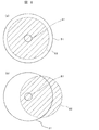
- FIG. 8 is a diagram for explaining the principle.
- FIG. 8 shows the secondary electron restricting plate 31 viewed from the sample 23 side, and is provided with an electron beam passage opening 81 (high angle side electron passage opening).
- FIG. 8A shows a state where the center of the dispersion range 82 of electrons emitted from the sample coincides with the electron beam passage aperture 81
- FIG. 8B shows the dispersion of electrons emitted from the sample.
- the center of the range 82 shows a state of being separated from the electron beam passage opening 81.
- the detection efficiency of the lower detector 28 (b) can be increased. According to the present embodiment apparatus, it is possible to suppress a decrease in detection efficiency even when the trajectory of secondary electrons is changed.
- the energy filter 34 includes, for example, a plurality of mesh electrodes and generates an electric field that repels electrons emitted from the sample. By changing the electric field strength, it is provided to selectively introduce electrons of desired energy to the detector side.
- the energy filter 34 is installed closer to the electron source 11 than the secondary electron limiting plate 31.
- the energy filter 34 is generally provided with holes and pipes for securing a passage path of primary electrons, and it is necessary to prevent high-angle secondary electrons (a) from entering the holes and pipes. is there. Therefore, similarly, a secondary electron aligner I32 is provided to control the deflection of the angle of the secondary electrons entering the energy filter 34.
- the angle of the high-angle secondary electron 2 (a) that has passed through the secondary electron aperture 31 is controlled by the secondary electron aligner II (L) 33 (a) and the secondary electron aligner II (U) 33 (b). Therefore, the approach angle with respect to the energy filter 35 can be kept constant by the secondary electron aligner I32. As a result, the effect of making the energy resolution of the energy filter constant can also be obtained.
- both the angle discrimination and the energy discrimination are compatible, but the secondary electron restriction plate 31 may be removed in order to perform only the energy discrimination.
- the concept of the control method of the secondary electron aligner II 33 (a), 33 (b) is shown in FIG.
- Primary electrons are irradiated to the off-axis position Ls of the sample surface.
- High-angle secondary electrons 2 (a) emitted therefrom travel in the opposite direction along the optical axis.
- Objective lens 17 receives the deflection action when passing through the image shift 25 and 26, enters the secondary electron aligner II (L) 33 (b) off-axis amount LL, at an angle theta SE.
- the secondary electron 2 (a) is deflected at an angle ⁇ L so as to pass through the center of the secondary electron aligner II (U) 33 (a).
- L SE defines the amount by which the secondary electrons 2 (a) are deflected by the image shift by the distance from the optical axis in the secondary electron limiting plate 31.
- LSE can be obtained by using a secondary electron arrival position detection method, which will be described later, or an electron trajectory simulation.
- Z SEAP is the height of the secondary electron limiting plate
- ⁇ L required for the secondary electron aligner II (L) 33 (b) is obtained as the following equation.
- FIG. 2 is described using a cross-sectional view, actually, it is necessary to control the azimuth direction in consideration of the rotation of the objective lens 17 due to the magnetic field.
- the rotation angle by a magnetic field is previously calculated
- the rotation angle by the magnetic field can be obtained by using a secondary electron arrival position detection method described later or an electron trajectory simulation.
- FIG. 3 shows a method of controlling the deflection to the hole outside the optical axis in the secondary electron limiting plate 31. If the secondary electrons 2 (a) when the image shift is not used are controlled so that ⁇ L and ⁇ U are in the opposite direction at the same angle, only the position of the orbit can be shifted while maintaining the parallel to the optical axis. it can. In this principle, only the secondary electron trajectory is translated, so that it can be controlled independently of the image shift interlock. If the required amount of movement on the secondary electron limiting plate is L SHIFT , a translation term can be added to the equations (4) and (5).
- the secondary electrons 2 (a) are caused by the focusing action of the magnetic lens and the electrostatic lens. It converges on the limiting plate 31.
- the image of the hole of the secondary electron limiting plate 31 is dark as shown in FIG. 4 (a) reflecting the shape of the secondary electron limiting plate. Can be obtained.
- the upper detector 28 (a) an image in which the hole of the secondary electron restricting plate 31 is bright is obtained as shown in FIG. 4 (b).
- the hole position in the screen reflects the scanning range on the secondary electron restricting plate 31, it changes when an image shift or a secondary electron aligner is used. Therefore, on the contrary, the image shift, the deflection sensitivity of the secondary electron aligner, and the angle in the azimuth direction can be obtained from the amount of change in the hole position. If the optical condition is not met, the secondary electrons 2 (a) do not converge at the secondary electron restricting plate 31, so that the outline of the hole appears blurred and it is difficult to confirm the hole position. In that case, the trajectory of secondary electrons may be traced by electron trajectory simulation.
- the secondary electron trajectory can be controlled with high accuracy even under various optical conditions. it can.
- a detector having a spatial resolution may be installed as the secondary electron limiting plate 31 to directly detect the secondary electron arrival position. Further, since the contrast of the hole is generated depending on whether or not it passes through the hole of the secondary electron restricting plate 31, if the signals detected by the upper detector 28 (a) and the lower detector 28 (b) are added, the hole You can eliminate the reflection of the shadow.
- FIG. 5 is a flowchart showing a process of forming a composite image using two detectors.
- the holder 24 is moved to hold the sample 23 at a desired observation position (step 501).
- an image shift is used within a range of several um (step 502).
- the control amount of (b) is calculated (step 503). If the control amount (operation condition such as deflection current or voltage) and the image shift amount (operation condition such as deflection current or voltage) are associated with each other and stored in a memory (not shown), the condition is reproduced later. be able to.
- the hole of the secondary electron restricting plate 31 may be on the optical axis and may be shared with the primary electron passage hole, or may be installed outside the optical axis.
- the image of the secondary electron restricting plate 31 is reflected in the image. The position appears at a position away from the center of the screen. For these deviations, the secondary electron arrival position is adjusted in advance based on the control equation (step 504).
- the secondary electron aligner I32 can be controlled so that the energy filter has a high entrance angle.
- the Wien conditions of the electric and magnetic fields are adjusted in advance and the deflection sensitivity is required.
- a scanning signal is input to the deflector to start scanning, and the signals detected by the upper detector 28 (a) and the lower detector 28 (b) are stored in the storage device 45 (step 505).
- the secondary electron trajectory is deflected by the sample charging. It is known that when an insulating sample is irradiated with primary electrons, the sample is positively or negatively charged when the number of incident primary electrons and the number of emitted secondary electrons differ. When the sample is charged, the secondary electrons are deflected by the electric field generated by the charge, so that the secondary electrons 2 (a) having a high angle component reach a position outside the hole of the secondary electron limiting plate 31, and the angle discrimination function is provided. descend.
- the secondary electron aligner II (U) 33 (a) and the secondary electron aligner II ( L) The control amount of 33 (b) is recalculated and output (step 507).
- the operator has set in advance whether or not to synthesize the image.
- the signals of the upper detector 28 (a) and the lower detector 28 (b) are arbitrarily calculated. Based on the equation, the image is formed after multiplication / addition / addition / subtraction (steps 508 and 509).
- image synthesis is not performed, two images detected by each detector can be acquired simultaneously.
- the upper detector 28 (a) detects a high angle component signal or an energy filtered high angle component signal
- the lower detector 28 (b) detects a low angle component signal.
- the upper detector 28 (a) detects information on the bottom of the pattern that is included in a large amount of high angle components
- the lower detector 28 (b) detects information on the top of the pattern that is included in a large amount of low angle components. It can be used to observe the upper part separately.
- the relationship of the energy resolution of the energy filter depends on the variation in the electric field and the variation in the incident angle of the electrons.
- the change in the incident angle of electrons changes the threshold energy of the energy filter, which causes variations in image contrast.
- the angle of the secondary electrons incident on the energy filter can be kept constant regardless of the use of the image shift, thereby stabilizing the contrast. Images can be acquired. Furthermore, as shown in FIG. 6, if the secondary electron aligner I32 is constituted by a two-stage Wien filter, the secondary electrons 2 (a) can be parallel to the optical axis when entering the energy filter 35. Ideal energy resolution can be expected when using a mesh / electrode.
- a method will be described in which a plurality of secondary electron aligners are arranged to cancel the aberration generated by the secondary electron aligner itself and to suppress the spread of primary electrons on the sample.
- An ideal Wien filter can deflect only secondary electrons without affecting the trajectory of the primary electrons.
- the electric field and magnetic field generated by the Wien filter do not always coincide with each other along the optical axis.
- the primary electrons have energy dispersion when emitted from the electron source, and orbital dispersion occurs when passing through the Wien filter, so that beam spread occurs on the sample.
- a technique is known in which a pair of equivalent Wien filters are arranged one above the other and deflected in the opposite direction.
- the secondary electron aligner II (U) 33 (a) and the secondary electron aligner II (L) 33 (b) are used in the direction to cancel, the generated aberration is small.
- another secondary electron aligner is provided above the reflector 27 that is not related to the control of the secondary electrons.
- the added secondary electron aligner is preferably controlled so as to always deflect at the same angle in the opposite direction to the secondary electron aligner I32 regardless of the trajectory of the secondary electrons.
- the amount used by the pair of secondary electron aligners is different, for example, when the secondary electron aligner II (U) 33 (a) or the secondary electron aligner II (L) 33 (b) is used, the remaining aberration is a concern. , It may be superimposed on the secondary electron aligner control so as to cancel it.
- FIG. 7 shows a cross section of an example of a device structure to be observed.
- the pattern 101 is a line-shaped pattern at the upper part, and a film 102 having a tapered hole pattern is provided below the pattern 101, and a film 103 is provided therebelow.
- this device structure is observed from the top with the upper detector 28 (a)
- an image with a bright contrast of the lower layer 103 is obtained as shown in FIG. 7 (a).
- the contrast of the top portion 101 is conversely enhanced as shown in FIG. 7 (b).
- the contrast of the line 101 is unnecessary unnecessary information. Therefore, the image brightness is multiplied and divided so that the brightness of the line portion 101 in FIGS. 7A and 7B is the same, and FIG. 7B is subtracted from FIG. . That is, a composite image is formed so as to cancel the contrast of a specific part of the image.
- eliminated the contrast of the line part 101 can be obtained.
- the dynamic range of brightness at the boundary portion between the intermediate layer 102 and the lower layer 103, which is a desired observation position can be expanded, and observation with high accuracy is possible. If the brightness of the composite image can be adjusted during image acquisition, the dynamic range can be optimized and the composite image can be acquired.
- the conversion electrode is used to detect the electron emitted from the sample after converting it to the tertiary electron.
- an MCP (Multi Channel Plate) detector is used instead of the conversion electrode.
- a detector that directly detects electrons emitted from such a sample may be used.
- the detector arranged in the lower stage serves as a blocking member that blocks low-angle components.
- the detection efficiency when the secondary electron restriction plate is used by controlling the trajectory of the secondary electrons is kept constant, and it is possible to always obtain an equivalent image even when using image shift. Become. Further, since the secondary electrons can enter the energy filter disposed on the upper stage of the secondary electron limiting plate at a certain angle, it is possible to stably acquire an image while keeping the energy resolution constant. become.
Landscapes
- Chemical & Material Sciences (AREA)
- Analytical Chemistry (AREA)
- Testing Or Measuring Of Semiconductors Or The Like (AREA)
- Analysing Materials By The Use Of Radiation (AREA)
Abstract
Description







12 引出電極
13 引出電圧
14 コンデンサレンズ
15 絞り
17 対物レンズ
18 加速円筒
20 ガイド
21 上走査偏向器
22 下走査偏向器
23 試料
24 ホルダー
25 上イメージシフト
26 下イメージシフト
27 反射板
28(a) 上検出器
28(b) 下検出器
31 2次電子制限板
32 2次電子アライナI
33(a) 2次電子アライナII(U)
33(b) 2次電子アライナII(L)
34 エネルギーフィルタ
Claims (11)
- 電子源と、当該電子源から放出される電子ビームの照射位置を偏向する偏向器と、当該偏向器を制御する制御装置を備えた走査電子顕微鏡において、
前記電子ビームの試料への照射によって得られる電子を検出する第1の検出器と、当該第1の検出器と前記偏向器との間に配置され、前記電子ビームの通過開口を有する開口形成部材と、前記試料から放出された電子を偏向する二次信号偏向器を備え、前記制御装置は、前記偏向器の偏向制御に応じて、前記試料から放出される電子を前記電子ビームの通過開口に向かって偏向するように前記二次信号偏向器を制御することを特徴とする走査電子顕微鏡。 - 請求項1において、
前記開口部形成部材は、電子の衝突によって電子を発生する変換電極であって、当該変換電極にて発生する電子を検出する第2の検出器を備えたことを特徴とする走査電子顕微鏡。 - 請求項1において、
前記開口部形成部材は、電子を検出する第2の検出器であることを特徴とする走査電子顕微鏡。 - 請求項1において、
第1の検出器より、前記電子ビーム光軸を中心として広い範囲に放出される電子を検出する第2の検出器と、前記第1の検出器と第2の検出器の出力を合成する演算器を備えたことを特徴とする走査電子顕微鏡。 - 請求項4において、
前記演算器は、前記第1の検出器と第2の検出器を出力を、特定のパターンのコントラストが等しくなるような処理を行い、当該特定パターンのコントラストを消去するように第1の検出器と第2の検出器の出力を合成することを特徴とする走査電子顕微鏡。 - 請求項1において、
前記偏向器は、前記電子ビームの走査位置を偏向するイメージシフト偏向器であって、前記制御装置は前記電子ビームの走査位置に応じて、前記二次信号偏向器を制御することを特徴とする走査電子顕微鏡。 - 請求項1において、
前記開口形成部材より電子源側にエネルギーフィルタが配置されることを特徴とする走査電子顕微鏡。 - 請求項7において、
前記エネルギーフィルタへの電子の入射角度を調整する偏向器を備えたことを特徴とする走査電子顕微鏡。 - 請求項1において、
前記前記偏向器の制御量と前記二次信号偏向器の動作条件を関連付けて記憶するメモリを備えていることを特徴とする走査電子顕微鏡。 - 請求項1において、
前記二次信号偏向器はウィーンフィルタであることを特徴とする走査電子顕微鏡。 - 電子源と、当該電子源から放出される電子ビームの照射位置を偏向する偏向器と、当該偏向器を制御する制御装置を備えた走査電子顕微鏡において、
前記電子ビームの試料への照射によって得られる電子を検出する第1の検出器と、当該第1の検出器より相対的に前記電子ビーム光軸を中心として広い範囲に放出される電子、或いは当該電子によってもたらされる電子を検出する第2の検出器と、当該第1の検出器と第2の検出器の出力を合成する演算部を備え、
当該演算部は、前記第1の検出器と第2の検出器の特定部位のコントラストを相殺するように前記出力の合成を実施することを特徴とする走査電子顕微鏡。
Priority Applications (2)
| Application Number | Priority Date | Filing Date | Title |
|---|---|---|---|
| US14/379,704 US9159529B2 (en) | 2012-02-28 | 2013-02-18 | Scanning electron microscope |
| KR1020147021505A KR101653080B1 (ko) | 2012-02-28 | 2013-02-18 | 주사 전자 현미경 |
Applications Claiming Priority (2)
| Application Number | Priority Date | Filing Date | Title |
|---|---|---|---|
| JP2012040865A JP5948084B2 (ja) | 2012-02-28 | 2012-02-28 | 走査電子顕微鏡 |
| JP2012-040865 | 2012-02-28 |
Publications (1)
| Publication Number | Publication Date |
|---|---|
| WO2013129147A1 true WO2013129147A1 (ja) | 2013-09-06 |
Family
ID=49082348
Family Applications (1)
| Application Number | Title | Priority Date | Filing Date |
|---|---|---|---|
| PCT/JP2013/053786 Ceased WO2013129147A1 (ja) | 2012-02-28 | 2013-02-18 | 走査電子顕微鏡 |
Country Status (4)
| Country | Link |
|---|---|
| US (1) | US9159529B2 (ja) |
| JP (1) | JP5948084B2 (ja) |
| KR (1) | KR101653080B1 (ja) |
| WO (1) | WO2013129147A1 (ja) |
Cited By (2)
| Publication number | Priority date | Publication date | Assignee | Title |
|---|---|---|---|---|
| WO2018131102A1 (ja) * | 2017-01-12 | 2018-07-19 | 株式会社 日立ハイテクノロジーズ | 荷電粒子線装置 |
| TWI778554B (zh) * | 2020-04-01 | 2022-09-21 | 日商日立全球先端科技股份有限公司 | 帶電粒子束裝置 |
Families Citing this family (18)
| Publication number | Priority date | Publication date | Assignee | Title |
|---|---|---|---|---|
| JP5663412B2 (ja) * | 2011-06-16 | 2015-02-04 | 株式会社日立ハイテクノロジーズ | 荷電粒子線装置 |
| JP6366127B2 (ja) * | 2013-12-12 | 2018-08-01 | 三星電子株式会社Samsung Electronics Co.,Ltd. | 電子線装置、試料観察方法 |
| WO2016142481A1 (en) * | 2015-03-10 | 2016-09-15 | Vladimir Petrovich Ovsyannikov | Method and device for the production of highly charged ions |
| JP2018174016A (ja) * | 2015-07-29 | 2018-11-08 | 株式会社日立ハイテクノロジーズ | 荷電粒子線装置 |
| US10651004B2 (en) * | 2016-03-31 | 2020-05-12 | Hitachi, Ltd. | Charged particle beam device |
| US11282671B2 (en) | 2016-07-28 | 2022-03-22 | Hitachi High-Tech Corporation | Charged-particle beam apparatus |
| GB201700936D0 (en) | 2017-01-19 | 2017-03-08 | Univ Bath | Optical fibre apparatus and method |
| US9934933B1 (en) * | 2017-01-19 | 2018-04-03 | Kla-Tencor Corporation | Extractor electrode for electron source |
| JP6932050B2 (ja) * | 2017-09-01 | 2021-09-08 | 株式会社日立ハイテク | 走査電子顕微鏡 |
| JP7105321B2 (ja) * | 2018-12-25 | 2022-07-22 | 株式会社日立ハイテク | 荷電粒子線装置 |
| WO2020193102A1 (en) * | 2019-03-27 | 2020-10-01 | Asml Netherlands B.V. | System and method for alignment of secondary beams in multi-beam inspection apparatus |
| JP7431136B2 (ja) | 2020-10-09 | 2024-02-14 | 株式会社日立ハイテク | 荷電粒子線装置、及び制御方法 |
| JP2022112137A (ja) * | 2021-01-21 | 2022-08-02 | 株式会社日立ハイテク | 荷電粒子ビーム装置 |
| WO2022219699A1 (ja) * | 2021-04-13 | 2022-10-20 | 株式会社日立ハイテク | 透過型電子顕微鏡 |
| US12688992B2 (en) * | 2021-04-16 | 2026-07-21 | Hitachi High-Tech Corporation | Electron beam application device |
| KR20230068893A (ko) * | 2021-11-11 | 2023-05-18 | 삼성전자주식회사 | 주사 전자 현미경(Scannig Electron Microscope, 이하 SEM), SEM을 동작시키는 방법 및 이를 이용한 반도체 소자를 제조하는 방법 |
| US20240128051A1 (en) * | 2022-10-14 | 2024-04-18 | Carl Zeiss Multisem Gmbh | Multi-beam charged particle beam system with anisotropic filtering for improved image contrast |
| CN121153098A (zh) * | 2023-05-08 | 2025-12-16 | Asml荷兰有限公司 | 补偿扫描带电粒子光学装置的收集变化 |
Citations (3)
| Publication number | Priority date | Publication date | Assignee | Title |
|---|---|---|---|---|
| JP2006114426A (ja) * | 2004-10-18 | 2006-04-27 | Hitachi High-Technologies Corp | 試料観察方法及び電子顕微鏡 |
| JP2006228999A (ja) * | 2005-02-18 | 2006-08-31 | Hitachi High-Technologies Corp | 荷電粒子ビームによる検査方法および検査装置 |
| JP2011247808A (ja) * | 2010-05-28 | 2011-12-08 | Toshiba Corp | 欠陥検査方法および欠陥検査装置 |
Family Cites Families (5)
| Publication number | Priority date | Publication date | Assignee | Title |
|---|---|---|---|---|
| JP4048925B2 (ja) * | 2002-11-18 | 2008-02-20 | 株式会社日立製作所 | 電子顕微鏡 |
| JP4920385B2 (ja) * | 2006-11-29 | 2012-04-18 | 株式会社日立ハイテクノロジーズ | 荷電粒子ビーム装置、走査型電子顕微鏡、及び試料観察方法 |
| JP4969231B2 (ja) * | 2006-12-19 | 2012-07-04 | 株式会社日立ハイテクノロジーズ | 試料電位情報検出方法及び荷電粒子線装置 |
| JP5241168B2 (ja) * | 2007-08-09 | 2013-07-17 | 株式会社日立ハイテクノロジーズ | 電子顕微鏡 |
| JP5519421B2 (ja) | 2010-06-15 | 2014-06-11 | 株式会社日立ハイテクノロジーズ | 走査型電子顕微鏡及びその制御方法 |
-
2012
- 2012-02-28 JP JP2012040865A patent/JP5948084B2/ja active Active
-
2013
- 2013-02-18 KR KR1020147021505A patent/KR101653080B1/ko active Active
- 2013-02-18 US US14/379,704 patent/US9159529B2/en active Active
- 2013-02-18 WO PCT/JP2013/053786 patent/WO2013129147A1/ja not_active Ceased
Patent Citations (3)
| Publication number | Priority date | Publication date | Assignee | Title |
|---|---|---|---|---|
| JP2006114426A (ja) * | 2004-10-18 | 2006-04-27 | Hitachi High-Technologies Corp | 試料観察方法及び電子顕微鏡 |
| JP2006228999A (ja) * | 2005-02-18 | 2006-08-31 | Hitachi High-Technologies Corp | 荷電粒子ビームによる検査方法および検査装置 |
| JP2011247808A (ja) * | 2010-05-28 | 2011-12-08 | Toshiba Corp | 欠陥検査方法および欠陥検査装置 |
Cited By (3)
| Publication number | Priority date | Publication date | Assignee | Title |
|---|---|---|---|---|
| WO2018131102A1 (ja) * | 2017-01-12 | 2018-07-19 | 株式会社 日立ハイテクノロジーズ | 荷電粒子線装置 |
| US11056310B2 (en) | 2017-01-12 | 2021-07-06 | Hitachi High-Tech Corporation | Charged-particle beam device |
| TWI778554B (zh) * | 2020-04-01 | 2022-09-21 | 日商日立全球先端科技股份有限公司 | 帶電粒子束裝置 |
Also Published As
| Publication number | Publication date |
|---|---|
| KR20140119079A (ko) | 2014-10-08 |
| US9159529B2 (en) | 2015-10-13 |
| JP2013178880A (ja) | 2013-09-09 |
| JP5948084B2 (ja) | 2016-07-06 |
| US20150014531A1 (en) | 2015-01-15 |
| KR101653080B1 (ko) | 2016-09-09 |
Similar Documents
| Publication | Publication Date | Title |
|---|---|---|
| JP5948084B2 (ja) | 走査電子顕微鏡 | |
| USRE49784E1 (en) | Apparatus of plural charged-particle beams | |
| US9035249B1 (en) | Multi-beam system for high throughput EBI | |
| US9437395B2 (en) | Method and compound system for inspecting and reviewing defects | |
| KR101759186B1 (ko) | 하전 입자선 장치 | |
| US9000395B2 (en) | Energy filter for charged particle beam apparatus | |
| US9984848B2 (en) | Multi-beam lens device, charged particle beam device, and method of operating a multi-beam lens device | |
| US8519334B2 (en) | Scanning electron microscope and sample observation method | |
| JP4920385B2 (ja) | 荷電粒子ビーム装置、走査型電子顕微鏡、及び試料観察方法 | |
| JP2015216086A (ja) | 荷電粒子線装置及び当該装置を用いる検査方法 | |
| JPWO2017168482A1 (ja) | 荷電粒子線装置、及び荷電粒子線装置の調整方法 | |
| JP2004342341A (ja) | ミラー電子顕微鏡及びそれを用いたパターン欠陥検査装置 | |
| US9048063B1 (en) | Electron beam apparatus | |
| WO2024115029A1 (en) | Systems and methods of energy discrimination of backscattered charged-particles | |
| JP2012230919A (ja) | 荷電粒子線の照射方法及び荷電粒子線装置 | |
| JP4658783B2 (ja) | 試料像形成方法 | |
| JP5400339B2 (ja) | 電子線応用装置 | |
| JP4110042B2 (ja) | 基板検査装置、基板検査方法および半導体装置の製造方法 | |
| JP4792074B2 (ja) | 基板検査方法および基板検査装置 | |
| JPH1173905A (ja) | パターン検査装置 | |
| JP3814968B2 (ja) | 検査装置 | |
| WO2025104896A1 (ja) | 欠陥検査装置 | |
| WO2025069195A1 (ja) | 荷電粒子ビーム装置 | |
| EP2182543A1 (en) | Method and device for improved alignment of a high brightness charged particle gun | |
| JP2006349691A (ja) | 基板検査装置、基板検査方法および半導体装置の製造方法 |
Legal Events
| Date | Code | Title | Description |
|---|---|---|---|
| 121 | Ep: the epo has been informed by wipo that ep was designated in this application |
Ref document number: 13754010 Country of ref document: EP Kind code of ref document: A1 |
|
| ENP | Entry into the national phase |
Ref document number: 20147021505 Country of ref document: KR Kind code of ref document: A |
|
| WWE | Wipo information: entry into national phase |
Ref document number: 14379704 Country of ref document: US |
|
| NENP | Non-entry into the national phase |
Ref country code: DE |
|
| 122 | Ep: pct application non-entry in european phase |
Ref document number: 13754010 Country of ref document: EP Kind code of ref document: A1 |