WO2013121767A1 - 光学センサ及び画像形成装置 - Google Patents
光学センサ及び画像形成装置 Download PDFInfo
- Publication number
- WO2013121767A1 WO2013121767A1 PCT/JP2013/000731 JP2013000731W WO2013121767A1 WO 2013121767 A1 WO2013121767 A1 WO 2013121767A1 JP 2013000731 W JP2013000731 W JP 2013000731W WO 2013121767 A1 WO2013121767 A1 WO 2013121767A1
- Authority
- WO
- WIPO (PCT)
- Prior art keywords
- light
- light receiving
- receiving element
- light emitting
- emitting element
- Prior art date
- Legal status (The legal status is an assumption and is not a legal conclusion. Google has not performed a legal analysis and makes no representation as to the accuracy of the status listed.)
- Ceased
Links
Images


Classifications
-
- G—PHYSICS
- G01—MEASURING; TESTING
- G01N—INVESTIGATING OR ANALYSING MATERIALS BY DETERMINING THEIR CHEMICAL OR PHYSICAL PROPERTIES
- G01N21/00—Investigating or analysing materials by the use of optical means, i.e. using sub-millimetre waves, infrared, visible or ultraviolet light
- G01N21/17—Systems in which incident light is modified in accordance with the properties of the material investigated
- G01N21/55—Specular reflectivity
-
- G—PHYSICS
- G03—PHOTOGRAPHY; CINEMATOGRAPHY; ANALOGOUS TECHNIQUES USING WAVES OTHER THAN OPTICAL WAVES; ELECTROGRAPHY; HOLOGRAPHY
- G03G—ELECTROGRAPHY; ELECTROPHOTOGRAPHY; MAGNETOGRAPHY
- G03G15/00—Apparatus for electrographic processes using a charge pattern
- G03G15/01—Apparatus for electrographic processes using a charge pattern for producing multicoloured copies
- G03G15/0142—Structure of complete machines
- G03G15/0178—Structure of complete machines using more than one reusable electrographic recording member, e.g. one for every monocolour image
- G03G15/0189—Structure of complete machines using more than one reusable electrographic recording member, e.g. one for every monocolour image primary transfer to an intermediate transfer belt
-
- G—PHYSICS
- G03—PHOTOGRAPHY; CINEMATOGRAPHY; ANALOGOUS TECHNIQUES USING WAVES OTHER THAN OPTICAL WAVES; ELECTROGRAPHY; HOLOGRAPHY
- G03G—ELECTROGRAPHY; ELECTROPHOTOGRAPHY; MAGNETOGRAPHY
- G03G15/00—Apparatus for electrographic processes using a charge pattern
- G03G15/50—Machine control of apparatus for electrographic processes using a charge pattern, e.g. regulating differents parts of the machine, multimode copiers, microprocessor control
- G03G15/5054—Machine control of apparatus for electrographic processes using a charge pattern, e.g. regulating differents parts of the machine, multimode copiers, microprocessor control by measuring the characteristics of an intermediate image carrying member or the characteristics of an image on an intermediate image carrying member, e.g. intermediate transfer belt or drum, conveyor belt
- G03G15/5058—Machine control of apparatus for electrographic processes using a charge pattern, e.g. regulating differents parts of the machine, multimode copiers, microprocessor control by measuring the characteristics of an intermediate image carrying member or the characteristics of an image on an intermediate image carrying member, e.g. intermediate transfer belt or drum, conveyor belt using a test patch
-
- G—PHYSICS
- G01—MEASURING; TESTING
- G01N—INVESTIGATING OR ANALYSING MATERIALS BY DETERMINING THEIR CHEMICAL OR PHYSICAL PROPERTIES
- G01N21/00—Investigating or analysing materials by the use of optical means, i.e. using sub-millimetre waves, infrared, visible or ultraviolet light
- G01N21/17—Systems in which incident light is modified in accordance with the properties of the material investigated
- G01N21/55—Specular reflectivity
- G01N2021/556—Measuring separately scattering and specular
Definitions
- the present invention relates to an optical sensor that irradiates a surface to be irradiated of a measurement object to which toner is attached with light from a light emitting element and detects the reflected light by a light receiving element, and an image forming apparatus including the same.
- the image forming apparatus of the electrophotographic system changes the image density and color registration due to changes in the environmental conditions in which the apparatus is placed, deterioration of the photoconductor and developer over time, and temperature changes in the apparatus. As it is, such a high requirement value cannot be satisfied.
- test pattern A test toner image (hereinafter referred to as a “test pattern”) is formed on a circulating moving body such as a photosensitive member, an intermediate transfer member, and a transfer conveyance belt, and the density and relative position of the test pattern are used as a toner detection device. Measure with an optical sensor.
- the image density and color registration are controlled so that the image density and color registration at the time of actual printing are appropriate based on the measurement results and the conditions when the test pattern is formed.
- factors for example, an exposure pattern at the time of forming a latent image, an exposure writing position, an image forming magnification, a developing bias, a charging bias, and the like are controlled.
- a sensor that optically measures the toner amount or the position of the toner image from the light reflected by irradiating the test pattern with light is often used.
- infrared light is used as the irradiation light.
- the reflection characteristics differ depending on the type of toner colorant.
- Patent Document 1 discloses a toner amount (that is, developer concentration) using a sensor that detects regular reflected light and scattered reflected light (scattered reflected light). There is a disclosure of a method for detecting the above.
- Patent Document 1 as an optical element, a light emitting element (LED) that irradiates light on an irradiated surface of a measurement object, a light receiving element for receiving specularly reflected light, and a scattered reflected light are received.
- An optical sensor having one light receiving element is described.
- Each light emitting element and light receiving element is a so-called bullet type optical element, and is provided with a semiconductor chip having a light emitting part or a light receiving part, a bullet type lens part, and a lead frame connected to a circuit board.
- This bullet-type optical element can change the direction of the element to some extent by changing the angle at which the lead frame is bent. For this reason, in patent document 1, each optical element is fitted to a housing so that the direction of each optical element becomes a desired direction.
- the bullet-type optical element has a certain length of lead frame so that the direction of the element can be changed, and because it has a lens part, it requires a certain volume from the semiconductor chip to the circuit board. Then it is disadvantageous.
- Patent Document 2 discloses an optical sensor using an optical element that is a chip component of the type mounted on the surface of a circuit board.
- an optical element of a type that is directly mounted on the surface (mounting surface) of the circuit board is used, since there is no lead frame or lens portion, it is required when the optical element is directly mounted on the circuit board.
- the volume of the sensor can be greatly reduced, and the sensor can be miniaturized.
- an optical sensor in which an optical element of a chip part is directly mounted on a surface (mounting surface) of a circuit board is fitted with the optical element in a housing different from the circuit board. It cannot be fixed. For this reason, disturbance light tends to occur due to light leaking in the circuit board or between the circuit board and the housing, and it is necessary to devise light shielding. Therefore, an object of the present invention is to improve the light shielding property of an optical sensor in which an optical element is mounted on the surface (mounting surface) of a circuit board.
- a typical configuration of the present invention for achieving the object includes a light emitting element that irradiates light to an irradiated surface, and a light receiving element that receives reflected light that is irradiated from the light emitting element and reflected by the irradiated surface.
- the light emitting element and the light receiving element have a circuit board disposed on the same mounting surface, and a housing attached to the circuit board, and the reflected light does not pass through the lens from the irradiated surface.
- the housing includes a light shielding wall disposed between the light emitting element and the light receiving element.
- the light shielding wall is fitted into a hole provided between the light emitting element and the light receiving element of the circuit board.
- Another representative configuration of the present invention includes a light emitting element that irradiates light to an irradiated surface, and first and second light receiving elements that receive reflected light irradiated from the light emitting element and reflected by the irradiated surface.
- An element a circuit board on which the light emitting element and the first and second light receiving elements are arranged on the same mounting surface, and a housing attached to the circuit board, and the reflected light is irradiated
- An optical sensor that is incident on the first and second light receiving elements without passing through the lens from the surface, and in which the optical axes of the light emitting element, the first and second light receiving elements are orthogonal to the mounting surface
- the housing includes a light shielding wall disposed between the light emitting element and the first light receiving element and between the first light receiving element and the second light receiving element, respectively.
- Another representative configuration of the present invention includes a light emitting element that irradiates light to an irradiated surface, and first and second light receiving elements that receive reflected light irradiated from the light emitting element and reflected by the irradiated surface.
- the housing includes a light shielding wall disposed between the light emitting element and the first light receiving element and between the light emitting element and the second light receiving element.
- FIG. 1 is an explanatory cross-sectional view illustrating the configuration of an image forming apparatus including a toner detection device according to the present invention.
- FIG. 2 is a block diagram illustrating the configuration of the control system of the image forming apparatus according to the present invention.
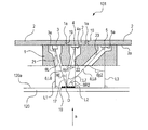
- FIG. 3 is an explanatory perspective view illustrating the configuration of the toner detection device according to the first exemplary embodiment of the present invention.
- FIG. 4 is an explanatory cross-sectional view illustrating the configuration of the first embodiment of the toner detection device according to the present invention.
- FIG. 5A is an exploded perspective view and an assembled perspective view illustrating the configuration of the first embodiment of the toner detection device according to the present invention.
- FIG. 5B is an exploded perspective view and an assembled perspective view illustrating the configuration of the first embodiment of the toner detection device according to the present invention.
- FIG. 6 is a diagram for explaining an electric circuit configuration of the toner detection device according to the present invention.
- FIG. 7 is an explanatory cross-sectional view for explaining the configuration of the first embodiment of the toner detection device according to the present invention.
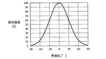
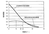
- FIG. 8A is a diagram showing the light emission intensity with respect to the irradiation angle of the light emitting element of the toner detection device according to the present invention.
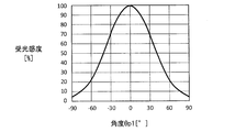
- FIG. 8B is a diagram showing the light receiving sensitivity of the light receiving element with respect to the irradiation angle of the light emitting element of the toner detection device according to the present invention.
- FIG. 9 is a diagram illustrating various characteristics of the first embodiment, the other embodiments 1, the second embodiment, and the other embodiments 2.
- FIG. 10 is a cross-sectional explanatory diagram illustrating the configuration of the toner detection device according to the first exemplary embodiment.
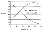
- FIG. 11 shows a first light receiving element that receives specularly reflected light with respect to an inclination angle of a circuit board with respect to a plane including a reflecting surface of a measurement object in the first embodiment, and a second light receiving element that receives scattered reflected light. It is a figure which shows each relative sensitivity.
- FIG. 11 shows a first light receiving element that receives specularly reflected light with respect to an inclination angle of a circuit board with respect to a plane including a reflecting surface of a measurement object in the first embodiment, and a second light receiving element that receives scattered reflected light. It is a figure which shows each relative sensitivity.
- FIG. 11 shows a first light receiving element that receives specularly reflected light with respect to an
- FIG. 12 is an explanatory cross-sectional view showing a configuration of an optical sensor for setting the irradiation intensity of the light emitting element and the reference level of the light receiving intensity of the regular reflection light and the scattered reflection light of the light receiving element.
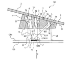
- FIG. 13 is a cross-sectional explanatory view illustrating the configuration of the toner detection device according to the second embodiment of the present invention.
- FIG. 14 shows a first light receiving element that receives specularly reflected light with respect to an inclination angle of a circuit board with respect to a plane including a reflecting surface of a measurement object in Embodiment 2, and a second light receiving element that receives scattered reflected light. It is a figure which shows each relative sensitivity.
- FIG. 15 is a cross-sectional explanatory diagram illustrating the configuration of a toner detection device according to another second embodiment.
- FIG. 16 is a cross-sectional explanatory view illustrating the configuration of the toner detection device according to the third embodiment of the present invention.
- FIG. 17 is a cross-sectional explanatory view illustrating the configuration of the toner detection device according to the fourth embodiment of the present invention.
- FIG. 18 is a cross-sectional explanatory view illustrating the configuration of another image forming apparatus including the toner detection device according to the present invention.
- Embodiment 1 of an image forming apparatus equipped with a toner detection device according to the present invention will be described with reference to FIGS.
- the first station is a yellow Y color toner image forming station
- the second station is a magenta M color toner image forming station
- the third station is a cyan C color toner image forming station
- the fourth station is a black K color toner image forming station.
- the first station includes a photosensitive drum 101Y as an image carrier.
- the photosensitive drum 101Y is formed by laminating a plurality of functional organic materials including a carrier generation layer that generates a charge by exposure on a metal cylinder, a charge transport layer that transports the generated charge, and the like.
- the outermost layer has a low electrical conductivity and is almost an insulator.
- a charging roller 102Y is brought into contact with the photosensitive drum 101Y, and as the photosensitive drum 101Y rotates, the surface of the photosensitive drum 101Y is uniformly charged without being driven to rotate.
- the charging roller 102Y is applied with a DC voltage or a voltage superimposed with an AC voltage, and discharge is generated in a small air gap on the upstream and downstream side from the contact nip portion between the charging roller 102Y and the surface of the photosensitive drum 101Y.
- the photosensitive drum 101Y is charged.
- the cleaning unit 104Y for cleaning the transfer residual toner on the surface of the photosensitive drum 101Y, and the developing device 108Y as a developing unit include a developing roller 105Y, a non-magnetic one-component toner 107Y, and a regulating blade 113Y.
- the photosensitive drum 101Y, the charging roller 102Y, the cleaning unit 104Y, the developing roller 105Y, the toner 107Y, the regulating blade 113Y, and the developing device 108Y are an integrated process cartridge 109Y that is detachable from the image forming apparatus 47.
- the exposure apparatus 103Y is configured to have a scanner unit that scans laser light with a polygon mirror or a light-emitting diode (LED) array. Then, the exposure light beam 114Y modulated based on the image signal is irradiated onto the surface of the photosensitive drum 101Y.
- a scanner unit that scans laser light with a polygon mirror or a light-emitting diode (LED) array. Then, the exposure light beam 114Y modulated based on the image signal is irradiated onto the surface of the photosensitive drum 101Y.
- LED light-emitting diode
- the charging roller 102Y, the developing roller 105Y, and the primary transfer roller 119Y are connected to a charging bias power source 112Y, a developing bias power source 115Y, and a primary transfer bias power source 116Y, respectively.
- the charging bias power source 112Y is a voltage supply unit to the charging roller 102Y.
- the developing bias power source 115Y is a voltage supply unit to the developing roller 105Y.
- the primary transfer bias power supply 116Y is a voltage supply unit to the primary transfer roller 119Y.
- the above is the configuration of the first station for forming a yellow Y color toner image.
- the second, third, and fourth stations have the same configuration, and parts having the same functions as those of the first station are given the same reference numerals, and magenta color is indicated for each station at the end of the reference numerals. M, C indicating cyan, and K indicating black are assigned.
- each member may be described with reference to only numerals, with Y, M, C, and K typically omitted.
- a belt 120 as an intermediate transfer belt composed of an endless belt on which a toner image as a measurement object is formed is supported by three rollers, a secondary transfer counter roller 118, a tension roller 124, and an auxiliary roller 132, as stretching members.
- the tension roller 124 is applied with a force in a direction in which the belt 120 is tensioned by a biasing means such as a spring (not shown) so that an appropriate tension force is maintained on the belt 120.
- the secondary transfer counter roller 118 rotates in response to a rotational drive from a driving source, and the belt 120 wound around the outer periphery of the secondary transfer counter roller 118 rotates.
- the belt 120 moves in the forward direction at substantially the same speed with respect to the photosensitive drum 101.
- the belt 120 rotates in the direction of arrow a in FIG. 1, and the primary transfer roller 119 is disposed on the side opposite to the photosensitive drum 101 with the belt 120 interposed therebetween, and is driven to rotate as the belt 120 moves.
- a toner detection device 131 as an optical sensor is provided at a position facing the tension roller 124 and detects the test pattern 10 on the belt 120 (on the object to be measured). By measuring the timing at which the test pattern 10 is detected, registration control is performed to increase the image position accuracy during image formation, and the density of the image is controlled by detecting the toner density of the test pattern 10.
- a neutralizing member 117 is disposed downstream of the primary transfer roller 119 in the rotation direction of the belt 120.
- the auxiliary roller 132, the tension roller 124, the secondary transfer counter roller 118, and the charge removal member 117 are electrically grounded.
- Image forming operation of the image forming apparatus 47 will be described.
- the image forming apparatus 47 receives a print command from the standby state, the image forming operation starts.
- the photosensitive drum 101, the belt 120, etc. start rotating in the direction of the arrow in FIG. 1 at a predetermined process speed.
- the photosensitive drum 101 is uniformly charged on the charging roller 102 by a charging bias power source 112, and then an electrostatic latent image according to image information is formed by the exposure light beam 114 from the exposure device 103.
- the toner 107 in the developing device 108 is negatively charged by the regulating blade 113 and applied to the developing roller 105.
- the developing roller 105 is supplied with a bias voltage of ⁇ 300 V from the developing bias power supply 115.
- the electrostatic latent image is visualized by negative polarity toner.
- a toner image (toner image) of the first color (yellow Y in this embodiment) is formed on the surface of the photosensitive drum 101.
- the other magenta M, cyan C, and black K stations operate in the same manner.
- an electrostatic latent image by exposure is formed on each photosensitive drum 101 while delaying the writing signal from the controller at a certain timing for each color according to the distance between the primary transfer positions of each color.
- a DC (direct current) bias voltage having a polarity opposite to that of the toner is applied to each primary transfer roller 119.
- the sheet 129 stacked on the sheet cassette 123 is picked up by the feeding roller 121 and conveyed to the registration roller pair 122 by a conveying roller (not shown) in accordance with the toner image formation. Then, the sheet 129 is conveyed to a transfer nip portion that is a contact portion between the belt 120 and the secondary transfer roller 128 by the registration roller pair 122 in synchronization with the toner image on the belt 120.
- a secondary transfer bias power source 133 applies a bias having a polarity opposite to that of the toner to the secondary transfer roller 128, and the four-color multiple toner images carried on the belt 120 are secondarily transferred onto the sheet 129 all at once.
- the secondary transfer residual toner remaining on the belt 120 is charged by the residual toner charging roller 134 disposed in contact with the belt 120.
- the secondary transfer residual toner that has been charged moves to the image forming station while being on the belt 120, is reversely transferred to the photosensitive drum 101, and is stored in the waste toner container provided in the cleaning unit 104 of the image forming station. To be recovered.
- the sheet 129 is conveyed to a fixing device having a heating roller 125 and a pressure roller 126. After the unfixed toner image is fixed by heating and pressing in the fixing device, the image forming apparatus It is discharged out of 47.
- FIG. 2 is a block diagram illustrating the configuration of the control system of the image forming apparatus 47.
- the host computer 40 is responsible for issuing a print command to the image forming apparatus 47 and transferring the image data of the print image to the interface board 41.
- the interface board 41 converts the image data from the host computer 40 into exposure data and issues a print command to the DC controller 42.
- the DC controller 42 operates with power supplied from the low-voltage power supply 43. When a print command is received, the DC controller 42 starts an image forming sequence while monitoring the state of various sensors 53.
- the DC controller 42 is equipped with a CPU (Central Processing Unit), a memory, etc., not shown, and performs a pre-programmed operation. Specifically, the operation of various driving devices 56 such as a main motor, a developing device 108, and a driving device for the photosensitive drum 101 is controlled in synchronization with outputs of various sensors 53 and internal timers. Further, the color mode and the mono mode are identified, and the operations of the development / separation device 61 of the black development device and the development / separation device 60 of the color development device are controlled.
- the DC controller 42 controls the high-voltage power supply 44 with a pre-programmed control voltage, control current, and timing while monitoring applied voltages and currents of a plurality of high-voltage power supplies provided in the high-voltage power supply 44.
- the high-voltage power supply 44 is connected to various functional parts that control image formation.
- the charging roller 102 provided in each image forming station receives a high voltage from the high voltage power supply 44 and contacts or approaches the photosensitive drum 101 of each image forming station to charge the surface of the photosensitive drum 101 to a uniform potential. To play a role.
- This charging potential is controlled by the DC controller 42 controlling the high voltage generated in the high voltage power supply 44.
- the developing roller 105 provided in each image forming station and the transfer roller 119 provided in each image forming station are supplied with a high voltage from the high voltage power supply 44, and the applied voltage and applied current have appropriate transfer characteristics. It is controlled by the DC controller 42.
- the power control device 57 connected to the heating roller 125 is controlled to perform power control so that the temperature of the heating roller 125 maintains a predetermined temperature.
- a test pattern 10 composed of a toner image for color misregistration detection is formed on the belt 120 (on the irradiated surface) for each color in at least two rows.
- the test pattern 10 reaches the position of the toner detection device 131 by at least two later-described toner detection devices (optical sensors) 131 provided on both sides of the downstream portion of the belt 120. It is detected and output to the DC controller 42.
- the DC controller 42 detects the passage timing of the test pattern 10 based on the output from the toner detection device 131 and compares it with a predetermined timing, thereby comparing the relative color in the main scanning direction and the sub-scanning direction between the colors. A deviation amount, a magnification in the main scanning direction, a relative inclination, and the like are calculated. According to the result, color misregistration correction is performed on the output image so that the relative color misregistration amount of each color is reduced.
- Image misalignment can be corrected by controlling the exposure timing of the exposure apparatus 103.
- the DC controller 42 controls the exposure apparatus 103 so that the scanning speed is a predetermined value and the exposure light amount is a predetermined value, and at the same time, corrects the color shift by adjusting the writing timing.
- the DC controller 42 counts the write reference pulse from the exposure apparatus 103 and generates an image leading edge signal at the time of image formation to generate the image front end signal. Send to.
- exposure data is sent from the interface board 41 to the exposure apparatus 103 via the DC controller 42 for each line (one surface of the polygon mirror).
- the writing timing of each line can be changed by several dots. Therefore, it is possible to adjust the writing position in the main scanning direction orthogonal to the conveyance direction of the sheet 129. Further, for example, if the writing timing for one line is delayed, the entire image can be shifted by one line in the conveying direction side of the sheet 129, so that the writing position in the sub-scanning direction that is the conveying direction of the sheet 129 can be adjusted in units of one line. is there.
- the rotational phase difference of the polygon mirror which is a polygon mirror of the scanner provided in the exposure apparatus 103 between the image forming stations it is possible to align one line or less in the sub-scanning direction. Further, the main scanning magnification can be corrected by changing the clock frequency which is the reference for turning on / off the exposure data.
- the relative color misregistration amount is detected based on the output of the toner detecting device (optical sensor) 131 as described above, and the exposure apparatus is controlled based on the relative color misregistration amount.
- the image formation (exposure start) timing and the exposure reference clock By adjusting the image formation (exposure start) timing and the exposure reference clock, the color misregistration amount (registration) can be corrected.
- toner image density control will be described.
- the problem with the electrophotographic image forming apparatus 47 is that the toner image density varies depending on the temperature and humidity conditions in which the image forming apparatus 47 is used and the degree of use of each color image forming station.
- the toner image density of the test pattern 10 is detected, and the image forming factor is controlled to obtain desired characteristics.
- a test pattern 10 composed of toner images for detection of each color is formed on the outer peripheral surface of the belt 120, and this is read by the toner detection device 131.
- a CPU central processing unit in the DC controller 42 sets density factors such as a charging voltage, a developing voltage, and an exposure light amount to specific values, and starts printing of the test pattern 10.
- the test pattern 10 is generated by a personal computer (PC) if it is a host-based printer, and is imaged by the exposure device 103 via the exposure control device at a predetermined timing controlled by the CPU in the DC controller 42.
- the test pattern 10 may be generated by the DC controller 42.
- the test pattern 10 formed on the outer peripheral surface of the belt 120 is detected by a toner detection device (optical sensor) 131 described later.
- the DC controller 42 processes the output from the toner detection device.
- the received light amount signal of the toner detection device 131 is A / D (analog / digital) converted, then output to the DC controller 42, processed by the CPU in the DC controller 42, and a value corresponding to the toner image density is calculated. (Toner density is detected). Based on this result, each toner image density factor is determined. In some cases, the above-described toner image density detection is repeated with a newly set toner image density factor to optimize each toner image density factor.
- the setting results of these toner image density factors are stored in a memory in the DC controller 42, and are used for normal image formation or the next toner image density detection.
- the image forming process conditions such as the high pressure condition and the laser power are adjusted based on the output from the toner detecting device (feedback result of toner image density detection).
- the maximum density of each color is adjusted to a desired value and setting it to an appropriate development setting, it is possible to prevent occurrence of a defect called “fogging” in which unnecessary toner adheres to a white background portion.
- the color balance of each color is kept constant, and at the same time, it is significant to prevent scattering of overlaid characters and fixing failure due to excessive toner loading.
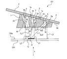
- Two toner detection devices 131 of the present embodiment are arranged side by side in the depth direction of FIG. 1 (the axial direction of the tension roller 124) so as to face the tension roller 124 with the belt 120 interposed therebetween.
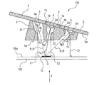
- the toner detection device 131 includes a light emitting element 3 that irradiates light to a detected portion (irradiated surface) D on the outer peripheral surface of the belt 120 that is a measurement object to which the toner 107 is attached. Furthermore, it has the 1st light receiving element 4 which receives the regular reflection light from the to-be-detected part D, and the 2nd light receiving element 5 which receives the scattered reflected light from the to-be-detected part D.
- the light emitting element 3 is composed of an LED (light emitting diode) and is directly mounted on the surface (mounting surface 2a) of the circuit board 2.
- the light emitting element 3 of the present embodiment uses an infrared light emitting diode SIM-030ST manufactured by Rohm, but other light emitting elements may be used.
- the light receiving elements 4 and 5 are photodiodes sensitive to the wavelength of light emitted from the light emitting element 3.
- an infrared light emitting diode SML-810TB manufactured by Rohm is used, but other optical elements such as photodiodes and phototransistors may be used.
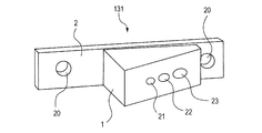
- the light emitting element 3 and the light receiving elements 4 and 5 are directly mounted (fixed) on the same mounting surface 2 a of the circuit board 2.
- the light emitted from the light emitting element 3 travels in the light guide path 21 of the housing 1 in the direction of the optical axis 6 and is irradiated to the detected part D on the outer peripheral surface of the belt 120.
- the specularly reflected light reflected by the detected portion D on the outer peripheral surface of the belt 120 travels substantially in the direction of the optical axis 7 and is guided into the light guide path 22 of the housing 1 to reach the light receiving element 4 for measuring the specularly reflected light. Detected.
- the irradiation light emitted from the light emitting element 3 is a test on the detected portion D on the outer peripheral surface of the belt 120. Scattered and reflected by the pattern 10. A part of the light is reflected in the direction of the optical axis 7 and reaches the light receiving element 4, and another part of the light is reflected in the direction of the optical axis 8 and reaches the light receiving element 5 for measuring the scattered reflected light. Is done.
- the light emitting element 3 and the light receiving elements 4 and 5 are not of a type in which lead pins extending from the elements are fixed (mounted) to the circuit board, such as bullet-type optical elements, but semiconductor chip components are used. It is a so-called bare chip type component that is directly mounted on the surface (mounting surface 2a) of the circuit board 2 (fixed in a state of being mounted on the mounting surface 2a). For this reason, unlike the type of element in which the bullet-type lead pin is fixed to the circuit board 2, the postures of the light emitting element 3 and the light receiving elements 4 and 5 cannot be freely changed.
- the light emitting surface 3 a of the light emitting element 3, the light receiving surface 4 a of the first light receiving element 4, and the light receiving surface 5 a of the second light receiving element 5 have errors that occur when mounted on the circuit board 2. Basically, it is parallel or substantially parallel to the surface (mounting surface 2a) of the mounted circuit board 2.
- the normal line 14 of the light emitting surface 3 a is the optical axis (optical center line) of the light emitting element 3
- the normal line 15 of the light receiving surface 4 a is the optical axis (optical center line) of the first light receiving element 4, and light is received.
- the normal 16 of the surface 5a is taken as the optical axis (optical center line) of the second light receiving element 5.
- the optical axes of the light emitting element 3, the first light receiving element 4, and the second light receiving element 5 are orthogonal or substantially orthogonal to the surface of the circuit board 2 (mounting surface 2a).
- the light emitting element 3 and the light receiving elements 4 and 5 are mounted on the surface of the circuit board 2 and fixed to each other by electrically connecting terminals to a wiring pattern formed on the circuit board 2.
- a general paper phenol board, glass epoxy board, or the like can be suitably used as the circuit board 2.
- FIG. 5A and 5B are perspective views of the toner detection device 131 of the present embodiment.
- FIG. 5A shows a state before the housing 1 described later is fixed to the circuit board 2.
- the light emitting element 3 and the light receiving elements 4 and 5 are mounted on the surface of the circuit board 2 by a known reflow method.
- Chip components which are the light emitting element 3 and the light receiving elements 4 and 5 are mounted on the circuit board 2 by die bonding. Thereafter, bonding is performed from the chip surface side to the wiring pattern on the circuit board 2 with a gold wire or an aluminum wire. It is also possible to form a bonding bump composed of protruding terminals arranged in an array on the chip surface and perform flip chip mounting on the circuit board 2. As shown in FIG. 5A, the light emitting element 3 and the light receiving elements 4 and 5 mounted on the circuit board 2 are arranged in a line.
- chip parts (not shown) are mounted on the circuit board 2, and current conversion applied to the light emitting element 3 and photoelectric conversion by the light receiving elements 4 and 5 are performed.
- a circuit having a function of converting the amplified current into a voltage and amplifying it is provided.
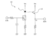
- FIG. 6 shows an example of the circuit configuration of the toner detection device 131. It has a light emitting element 3 made of LED and light receiving elements 4 and 5 made of phototransistors. The light emitting element 3 emits light to the outer peripheral surface of the belt 120, and the reflected light from the outer peripheral surface of the belt 120 is received by the light receiving elements 4 and 5. The detected current from the light receiving elements 4 and 5 is converted into a voltage V1 by an IV (current / voltage) conversion circuit, and is input to an AD conversion port of a CPU provided in the DC controller 42 shown in FIG. Is converted into digital data and used for calculation.
- IV current / voltage
- FIG. 5B is a perspective view showing the toner detection device 131 in a state where the housing 1 is fixed to the circuit board 2. As shown in FIG. 5B, the housing 1 is fixed to the circuit board 2.
- the housing 1 is made of a black resin mold having a high light shielding property.
- the housing 1 is provided with a light guide path (first light guide path) 21 that is an emission hole of the light emitting element 3, a light guide path (second light guide path) 22 that is a light receiving hole of the light receiving elements 4 and 5, and a light guide path (third).
- a light guide) 23 is provided.
- the portion of the housing 1 that forms the light guide path 21 functions as a diaphragm that restricts the light irradiated to the detected part D, and the part of the housing 1 that forms the light guide paths 22 and 23 reflects the reflected light from the detected part D. It functions as an aperture that regulates These diaphragms determine the light irradiation direction and the light receiving direction of the toner detection device 131.
- a straight line connecting the center of gravity of the light emitting surface 3 a of the light emitting element 3 and the center of gravity of the light guide 21 is defined as the optical axis 6 of the light emitting element 3.
- the optical axis 6 is different from the optical axis (optical center line) of the light emitting element 3 which is the normal line 14 of the light emitting surface 3a.
- the optical axis 6 is the optical axis (center ray) of the irradiation light irradiated from the light emitting element 3 to the detected part D.
- a straight line connecting the center of gravity of the light receiving surface 4a of the light receiving element 4 for regular reflection light and the center of gravity of the light guide path (second light guide path) 22 is defined as the optical axis 7 of the light receiving element 4 for regular reflection light.
- the optical axis 7 is different from the optical axis (optical center line) of the first light receiving element 4 which is the normal 15 of the light receiving surface 4a.
- the optical axis 7 is the optical axis (center ray) of the reflected light that is reflected by the detected part D and incident on the light receiving element 4.
- a straight line connecting the center of gravity of the light receiving surface 5a of the light receiving element 5 for scattered reflected light and the center of gravity of the light guide path (third light guide path) 23 is defined as the optical axis 8 of the light receiving element 5 for scattered reflected light.
- the optical axis 8 is the optical axis (center ray) of the reflected light that is reflected by the detected part D and incident on the light receiving element 5.
- This optical axis line 8 is different from the normal line 15 of the light receiving surface 5a with the optical axis (optical center line) of the second light receiving element 5.
- the light emitted from the light emitting element 3 reaches the light receiving elements 4 and 5 through the inside of the housing 1 and the circuit board 2 without being irradiated on the outer peripheral surface of the belt 120, the light is disturbing light ( Stray light), which increases measurement errors and is not preferable.
- the conventional bullet-type optical element described in Patent Document 1 Japanese Patent Application Laid-Open No. 2006-267644
- the light emitting element 3 and the light receiving elements 4 and 5 are mounted on the mounting surface of the circuit board 2 and the periphery thereof is covered with the housing 1, light easily leaks from the boundary portion between the circuit board 2 and the housing 1. Furthermore, there is no condensing optical element such as a lens in the optical element or the housing (no light emission or light reception through the lens). For this reason, the light emitting element emits light having low directivity that does not pass through the lens or the like, and light is emitted in various directions within the first light guide path of the housing. For this reason, light tends to go to the boundary portion between the circuit board 2 and the housing 1.
- a wall (light-shielding wall) 1a protrudes from the fixed surface of the housing 1 on the circuit board 2 side.
- the wall portion (light-shielding wall) 1 a of the housing 1 is inserted and fitted into the slit hole 19 provided through the circuit board 2. This prevents the light emitted from the light emitting element 3 from being transmitted to the light receiving elements 4 and 5 through the housing 1 or the circuit board 2 without irradiating the outer peripheral surface of the belt 120 and becoming disturbing light (stray light). Take a role.
- the wall portion 1 a and the slit hole 19 are provided between the light emitting element 3 and the light receiving element 4 and between the light receiving element 4 and the light receiving element 5. Therefore, the wall portion (light-shielding wall) 1a fits into the slit hole 19, so that the space between the light guide path 21 and the light guide path 22 in the housing 1 and the space between the light guide path 22 and the light guide path 23 are more reliable. Shield from light (block light from coming and going).
- the mounting surface 2 a of the circuit board 2 receives light for measuring scattered reflected light with respect to a plane (ridge line 120 a) including a reflective surface (irradiated surface) formed by the outer peripheral surface of the belt 120.
- the element 5 is disposed in a direction approaching the belt 120 with an inclination angle ⁇ k.
- a hole 20 is formed in the circuit board 2 and is fixed to a stay or the like of the image forming apparatus 47 by a fixing tool such as a screw (not shown).
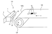
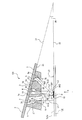
- FIG. 3 is a perspective view for explaining the arrangement of the toner detection device 131 of the present embodiment in the image forming apparatus 47.
- the toner detection device 131 is opposed to the portion where the belt 120 is wound around the tension roller 124.
- the toner detection device 131 is directed to a semi-cylindrical curved surface on the outer peripheral surface of the belt 120 wound around the tension roller 124, and the optical axes 6, 7, 8 of the light emitting element 3 and the light receiving elements 4, 5 are respectively tension rollers 124. It is arrange
- FIG. 4 is a sectional view in a plane including the optical axis 6 of the light emitting element 3 and the optical axes 7 and 8 of the light receiving elements 4 and 5.
- the tension roller 124 is driven to rotate in the direction of arrow R in FIG. 3 and rotates with the belt 120.
- a test pattern 10 made of a toner image is formed on the belt 120 and moves in the direction of arrow a in FIG.
- the test pattern 10 is formed on the belt 120 during calibration so that the test pattern 10 passes through the detected portion D on the outer peripheral surface of the belt 120 irradiated with light from the light emitting element 3 of the toner detection device 131. .
- the light emitted from the light emitting element 3 is reflected at a predetermined reflectivity determined according to the refractive index and surface state specific to the material of the belt 120 which is the base of the test pattern 10 and is detected by the light receiving elements 4 and 5.
- the belt 120 serving as a base of the test pattern 10 is hidden in a portion where the toner is present, and the amount of specular reflection from the belt 120 is reduced.
- the amount of toner in the test pattern 10 increases, the amount of light received by the light receiving element 4 for regular reflection light decreases. Based on this reduction ratio, the density of the test pattern 10 is obtained.
- the toner is a color toner other than black (yellow, magenta, cyan)
- the amount of specular reflection from the belt 120 decreases equally as the toner amount increases.
- the scattered reflected light from the toner increases, and the sum thereof becomes the amount of light received by the light receiving element 4 for regular reflected light.
- a light receiving element 5 for measuring only the scattered reflected light is arranged separately. Then, the amount of light received by the light receiving element 5 that measures only the scattered reflected light is subtracted from the amount of light received by the light receiving element 4 that is the sum of the amount of specularly reflected light and the amount of scattered reflected light. Thereby, the net specular reflection light amount can be calculated. Thereby, the density of the test pattern 10 can be measured even with a color toner other than black.
- the amount of reflected light also varies as the surface state of the outer peripheral surface of the belt 120 that is the base of the test pattern 10 varies depending on the degree of use of the belt 120 that is the measurement object. Therefore, it is preferable to normalize the amount of reflected light when the test pattern 10 is formed on the outer peripheral surface of the belt 120 based on the amount of reflected light when the test pattern 10 is not present on the outer peripheral surface of the belt 120.
- the light quantity of the light emitting element 3 is varied, the size of the irradiation spot in the detected portion D is varied, the sensitivity of the light receiving elements 4 and 5 is varied, and the light guides 21, 22, and 23 are soiled. Even if there is some, etc., sufficient detection accuracy can be secured.
- the test pattern 10 used for the calibration uses the toner 107 of the image forming apparatus 47. For this reason, the amount used is preferably as small as possible.
- test pattern 10 it is preferable to make the test pattern 10 as small as possible.
- the time resolution is related to the time constant of the detection circuit. In general, the higher the sensitivity of the sensor, the faster the response can be expected. Therefore, it is important to increase the sensitivity.
- the LED employed as the light emitting element 3 has a drift phenomenon in which the temperature of the internal semiconductor chip rises due to light emission and the light output fluctuates.
- the LED drive current can be lowered, the time for the drift phenomenon to converge (the influence can be ignored) is shortened, and calibration is required. It is preferable because time can be shortened.
- the toner detection device 131 is configured to detect regular reflection light and scattered reflection light from the detected portion D on the outer peripheral surface of the belt 120.
- the optical axis of the irradiation light emitted from the light emitting element 3 to the detected part D is the optical axis 6, and the optical axis 6 is incident at an angle ⁇ E with respect to the direction of the normal line 17 of the belt 120. Reflected by the belt 120.
- the angle ⁇ R1 and the angle ⁇ E between the optical axis 7 of the specularly reflected light and the normal line 17 of the belt 120 are the same. Further, when the angle ⁇ E is changed, the amount of specular reflection varies depending on the toner amount, that is, the density of the test pattern 10, and generally, when the angle ⁇ E is reduced, a higher density can be measured. However, if the angle ⁇ E is too small, the distance between the light emitting element 3 and the light receiving element 4 becomes short, and there is a problem that the design and arrangement of the light guide paths 21 and 22 become difficult. Therefore, the angle ⁇ E is preferably about 5 ° to 30 °, and in the present embodiment, the angle ⁇ E is set to 15 °.
- the detection of scattered reflected light if the regular reflected light reflected by the belt 120 from the light emitted from the light emitting element 3 enters the light receiving element 5 on the scattered reflected light side, the scattered reflected light cannot be measured correctly. For this reason, it is necessary to secure a certain angle between the optical axis 8 of the scattered reflected light entering the light receiving element 5 on the scattered reflected light side and the optical axis 7. That is, the angle ⁇ R2 between the optical axis 8 and the ridge line 120a of the belt 120 needs to avoid a value close to (90 ° ⁇ angle ⁇ E).
- the angle ⁇ R2 has a certain margin and the light receiving element 5 on the scattered reflected light side. It is preferable to set the angle so that the regular reflection light does not enter. Further, when the angle ⁇ E is about 5 ° to 30 °, it is difficult to dispose the light receiving element 5 between the light emitting element 3 and the light receiving element 4. That is, it is difficult to satisfy (angle ⁇ R2)> (90 ° ⁇ angle ⁇ E). Therefore, it is preferable to set the angle ⁇ R2 to about 35 ° to 60 °. In this embodiment, the angle ⁇ R2 is set to 45 °.
- the optical axis 6 is determined by the relationship between the light emitting surface 3a and the light guide path 21, the optical axis 6 and the light emitting surface 3a
- the light emission intensity is likely to change depending on the angle. This will be described.
- reference numeral 14 denotes a normal line to the light emitting surface 3a of the light emitting element 3 (or a mounting surface to the circuit board 2 on the back side of the light emitting element 3).
- An angle ⁇ L formed by the normal line 14 of the light emitting surface 3 a of the light emitting element 3 and the optical axis 6 is an angle that affects the amount of light emitted from the toner detection device 131.
- FIG. 8A shows the relationship between the angle ⁇ L formed by the normal line 14 of the light emitting surface 3 a of the light emitting element 3 and the optical axis 6 and the light emission intensity irradiated to the detected portion D on the outer peripheral surface of the belt 120 of the light emitting element 3.
- the light receiving sensitivity of the light receiving elements 4 and 5 is easily changed depending on the angle between the optical axes 7 and 8 and the light receiving surfaces 4a and 5a.
- the angle between the normal axis 15 of the light receiving surface 4a of the light receiving element 4 for receiving the regular reflected light and the optical axis 7 of the regular reflected light is ⁇ p1.
- FIG. 8B is a diagram showing a change in photocurrent when the light receiving element 4 is irradiated with constant light and the irradiation angle ⁇ p1 is changed.
- the angle ⁇ p1 formed by the optical axis 7 of the regular reflection light with respect to the direction of the normal 15 of the light receiving surface 4a of the light receiving element 4 is used at a large angle, the photocurrent decreases even if the same amount of light is received. Sensitivity deteriorates.
- the normal line 14 of the light emitting surface 3a coincides with the optical axis 6, and the light receiving elements 4 and 5 have the normal line 15 of the light receiving surface 4a and the normal line 16 of the light receiving surface 5a, respectively.
- the most ideal arrangement is coincident with the optical axes 7 and 8.
- the light emitting element 3 and the light receiving elements 4 and 5 are directly mounted on the surface of the common circuit board 2.
- the postures of the light-emitting element 3 and the light-receiving elements 4 and 5 cannot be freely changed, and the normal lines 14, 15, and 16 are substantially parallel, and in some cases, necessary detection accuracy cannot be ensured.
- the light receiving sensitivity when the light receiving sensitivity is lowered, it is conceivable to increase the amplification factor of the electric circuit and secure the dynamic range of the signal.
- the time constant generally increases, and it takes time for the output values from the light receiving elements 4 and 5 to converge to the original values.
- the temporal responsiveness does not deteriorate, and the required responsiveness may not be obtained under measurement conditions in which the test pattern 10 moves at a higher speed.
- the amount of light that enters the light receiving element 5 that detects scattered reflected light from the test pattern 10 made of a toner image enters the light receiving element 4 that detects regular reflected light from the belt 120. It is weaker than the amount of light.
- the direction of reflection of specularly reflected light is significantly limited compared to scattered reflected light. For this reason, even if the reflectance of the belt 120 is somewhat low, if the light receiving element 4 is arranged at the correct position, the rate of light reception is large, and the attenuation due to the distance between the light receiving element 4 and the belt 120 is also compared with the scattered reflected light. If you do it, there is little.
- the detection sensitivity of the toner detection device 131 is liable to be adversely affected when the light receiving sensitivity of the scattered reflected light by the light receiving element 5 is lower than the light receiving sensitivity of the light receiving element 4 for regular reflection light.
- the detection accuracy of the toner detection device 131 is improved while maintaining the angles of the detected portion D on the outer peripheral surface of the belt 120 and the optical axis 6, the optical axis 7, and the optical axis 8 as described above. Is to do.
- the mounting surface 2a of the circuit board 2 is disposed so as to be inclined (inclined by a predetermined angle) by a predetermined angle ⁇ k with respect to a plane (ridge line 120a) including the detected portion D on the outer peripheral surface of the belt 120.
- the light emitting element 3 and the first and second light receiving elements 4 and 5 are on the same plane and on the same straight line with a predetermined distance from each other. And disposed on the same circuit board 2 (on the circuit board).
- the light emitting surface 3 a of the light emitting element 3, the light receiving surface 4 a of the first light receiving element 4, and the light receiving surface 5 a of the second light receiving element 5 are constituted by the outer peripheral surface of the belt 120.
- a perpendicular is drawn with respect to the plane (ridgeline 120a) including the reflected surface (irradiated surface). And let the length of each perpendicular
- the length L3 of the perpendicular drawn from the light receiving surface 5a of the second light receiving element 5 to the plane (ridgeline 120a) including the reflecting surface (surface to be irradiated) composed of the outer peripheral surface of the belt 120 is the shortest.
- This is performed by placing the mounting surface 2a of the circuit board 2 so as to be inclined (inclined by a predetermined angle) by a predetermined angle ⁇ k with respect to the plane (ridge line 120a) including the detected portion D on the outer peripheral surface of the belt 120.
- the length of the perpendicular drawn from the light emitting surface 3a of the light emitting element 3 to the plane (ridgeline 120a) including the detected portion (irradiated surface) D on the outer peripheral surface of the belt 120 is L1.
- the length of the perpendicular line extending from the light receiving surface 4a of the first light receiving element 4 to the plane (ridgeline 120a) including the detected portion (irradiated surface) D on the outer peripheral surface of the belt 120 is L2.
- the length of the perpendicular line extending from the light receiving surface 5a of the second light receiving element 5 to the plane (ridgeline 120a) including the detected portion D on the outer peripheral surface of the belt 120 is L3.
- the light emitting element 3 and the first and second light receiving elements 4 and 5 are arranged so as to satisfy ⁇ L3 ⁇ L2 ⁇ L1 ⁇ .
- FIG. 11 is a diagram showing the light receiving sensitivity of specularly reflected light received by the light receiving element 4 and the light receiving sensitivity of scattered reflected light received by the light receiving element 5 with respect to the inclination angle ⁇ k of the mounting surface 2a of the circuit board 2 in this embodiment. is there.
- the graph shown in FIG. 11 takes into account the change in the light emission intensity of the light emitting element 3 in addition to the sensitivity of each of the light receiving elements 4 and 5 due to the inclination of the light receiving elements 4 and 5.
- the sensitivity shown in FIG. 11 is obtained by setting the light receiving sensitivity of the configuration shown in FIG. 11
- FIG. 12 is a cross-sectional explanatory view showing the configuration of an optical sensor for setting the reference level of the irradiation intensity of the light emitting element 3 and the received light intensity of the regular reflection light and scattered reflection light of the light receiving elements 4 and 5.
- the normal line of the light emitting surface 3 a of the light emitting element 3 coincides with the optical axis 6, the normal line of the light receiving surface 4 a of the light receiving element 4 coincides with the optical axis line 7, and the normal line of the light receiving surface 5 a of the light receiving element 5 coincides with the optical axis line 8.
- the angle ⁇ R2 between the optical axis 8 of the scattered reflected light entering the light receiving element 5 having the scattered reflection optical axis angle and the ridge line 120a of the belt 120 is 45 °, and the light emitting element 3 having the irradiation optical axis angle of the light emitting element 3
- the angle ⁇ E between the optical axis 6 and the normal line 17 of the belt 120 is 15 °.
- the angle ⁇ R1 between the optical axis 7 of the specularly reflected light entering the light receiving element 4 having the specularly reflected optical axis angle and the normal line 17 of the belt 120 is 15 °.
- the irradiation intensity at the detected part D from the light emitting surface 3a of the light emitting element 3 in the optical sensor shown in FIG. 12 is “1”. Further, the received light intensity of the regular reflection light at the light receiving element 4 at that time is set to “1”. Further, the received light intensity of the scattered reflected light at the light receiving element 5 at that time is set to “1”. Thereby, each reference level is set.
- the light receiving sensitivity of regular reflection light by the light receiving element 4 decreases as the inclination angle ⁇ k of the mounting surface 2a of the circuit board 2 increases. This is because as the inclination angle ⁇ k of the mounting surface 2a of the circuit board 2 increases, the light emission intensity of the light-emitting element 3 decreases and is affected.
- the sensitivity of the scattered reflected light by the light receiving element 5 gradually increases.
- the sensitivity of the scattered reflected light by the light receiving element 5 reaches a peak, and the inclination angle ⁇ k of the mounting surface 2a of the circuit board 2 exceeds 15 °.
- the sensitivity of the scattered reflected light by the light receiving element 5 gradually decreases.
- the inclination angle ⁇ k of the mounting surface 2a of the circuit board 2 with respect to the plane (ridgeline 120a) including the detected portion (irradiated surface) D of the outer peripheral surface (reflecting surface) of the belt 120 is larger than 0 degree, and It is preferable to set at an angle of 22 degrees or less.
- ⁇ k is 0 ° ⁇ k ⁇ 22 °
- the amount of light is sufficiently larger than the scattered reflected light. In fact, it can be used without problems.
- FIG. 10 shows a cross-sectional view of a toner detection device 131 of another embodiment 1. Components similar to those of the first embodiment described above are denoted by the same reference numerals and description thereof is omitted.
- the circuit board 2 is arranged in parallel with the ridgeline 120 a on the outer peripheral surface of the belt 120.
- the light receiving element whose angle ⁇ E between the optical axis 6 of the light emitting element 3 that is the irradiation optical axis angle of the light emitting element 3 and the normal line 17 of the belt 120 is 15 °, and whose light axis angle is the scattering reflection optical axis.
- the angle ⁇ R2 between the optical axis 8 of the scattered reflected light entering 5 and the ridge line 120a of the belt 120 was set to 45 °.
- the inclination angle ⁇ k of the mounting surface 2a of the circuit board 2 is 0 °.
- the angle ⁇ L of the optical axis 6 of the emitted light from the light emitting element 3 is 15 °
- the incident angle ⁇ p1 of the specularly reflected light to the light receiving element 4 is 15 °
- the incident angle ⁇ p2 of the scattered reflected light to the light receiving element 5 is 45 °.
- the first embodiment shown in FIG. 7 is compared with the other embodiment 1 shown in FIG.
- the optical axis 8 of the scattered reflected light entering the light receiving element 5 and the light receiving surface of the light receiving element 5 The angle ⁇ p2 with respect to the normal line 16 can be made smaller than in the other embodiment 1.
- the scattered reflected light entering the light receiving element 5 can be received at an angle with higher light receiving sensitivity, and the light receiving sensitivity of the scattered reflected light can be improved.
- the attenuation of light due to the distance is reduced, and the light receiving sensitivity of the scattered reflected light by the light receiving element 5 can be improved.
- the angle ⁇ p1 between the optical axis 7 and the normal 15 of the light receiving surface of the light receiving element 4 can be made smaller than in the other embodiment 1, and the light receiving sensitivity of the light receiving element 5 itself can be improved. I can do it.
- the angle ⁇ L between the optical axis 6 of the light emitted from the light emitting element 3 and the normal line 14 of the light emitting surface 3a of the light emitting element 3 is obtained. Since the distance between the light emitting element 3 and the belt 120 increases, the amount of light decreases.
- the distance of the light emitting element 3 from the belt 120 decreases the amount of light and the light receiving element 5 of scattered reflected light approaches the belt 120 and the sensitivity increases.
- the combined optical path length does not change significantly. Therefore, the amount of change due to the distance of the light emitting element 3 from the belt 120 is small.
- the light emitting element 3 has a low emission intensity on the light emitting side with a small change rate with respect to the angle ⁇ L of the optical axis 6. To do. For this reason, the improvement in the light receiving sensitivity due to the change in the angle ⁇ p2 of the optical axis 8 of the light receiving element 5 on the light receiving side has a higher improvement rate and the total sensitivity is improved.
- the sensitivity improving effect is that the distance L3 between the light receiving element 5 that receives the scattered reflected light on the circuit board 2 and the belt 120 is larger than the distance L1 between the light emitting element 3 on the circuit board 2 and the belt 120. Make it smaller. This is achieved by inclining the circuit board 2 with respect to the ridgeline 120a of the belt 120.
- the inclination angle ⁇ k between the extension line 31 of the plane (mounting surface 2a) of the circuit board 2 and the extension line 32 of the ridge line 120a of the belt 120 is determined by the optical axis 6 of the light emitting element 3 and the normal line 17 of the belt 120. It is most preferable in terms of sensitivity that the angle be approximately equal to the angle ⁇ E. If the tilt angle ⁇ k is tilted twice or more of the angle ⁇ E, the effect of improving the sensitivity is lost. Therefore, the tilt angle ⁇ k is preferably less than twice the angle ⁇ E.
- the angle ⁇ E between the optical axis 6 of the light emitting element 3 that is the irradiation optical axis angle of the light emitting element 3 and the normal line 17 of the belt 120 is 15 °, and the light receiving element 5 that is the scattered reflection optical axis angle.
- the angle ⁇ R2 between the optical axis 8 of the scattered reflected light entering and the ridge line 120a of the belt 120 was set to 45 °.
- the inclination angle ⁇ k of the circuit board 2 When the inclination angle ⁇ k of the circuit board 2 is set to 15 °, the angle ⁇ L of the optical axis 6 from the light emitting element 3 is 30 °, the incident angle ⁇ p1 of the specularly reflected light to the light receiving element 4 is 0 °, and the scattered reflected light is received.
- the incident angle ⁇ p2 to the element 5 was 30 °.
- the angle ⁇ R1 between the optical axis 7 of the specularly reflected light and the normal line 17 of the belt 120 is substantially the same as the angle ⁇ E between the optical axis 6 of the light emitting element 3 and the normal line 17 of the belt 120. Is preferred. Therefore, the angle ⁇ R2 between the angle ⁇ E, the optical axis 8 of the light receiving element 5 and the ridgeline 120a of the belt 120, the extension line 31 of the plane of the circuit board 2, and the extension line 32 of the ridgeline 120a of the belt 120. Is determined.
- the other angles ⁇ R1, ⁇ L, ⁇ p1 and ⁇ p2 and the belt 120 and the light receiving element 5 for scattered reflected light are naturally determined.
- FIG. 9 shows a table for explaining the characteristics of the toner detection device 131 according to the first embodiment, the other embodiments 1, the second embodiment described later, and the second embodiment 2 described later.
- L7 shown in FIG. 9 is the distance on the optical axis 7 from the light receiving element 4 to the belt 120 of the regular reflection light shown in FIG. 7, and is 10 mm in the first embodiment.
- L6 shown in FIG. 9 is a distance on the optical axis 6 from the light emitting element 3 to the belt 120 shown in FIG. 7, and was 11.5 mm in the first embodiment.
- L8 shown in FIG. 9 is the distance on the optical axis 8 from the light receiving element 5 to the belt 120 of the scattered reflected light shown in FIG. 7, and was 11.5 mm in the first embodiment.
- the sensitivity of the amount of light entering the light receiving element 4 for specularly reflected light was sufficiently high and there was no problem.
- the sensitivity of the amount of scattered reflected light entering the light receiving element 5 was 0.24 times the reference level, which is the sensitivity of the optical sensor shown in FIG.
- FIG. 9 shows a table for explaining the characteristics of the toner detection device 131 of the first embodiment.
- L7 shown in FIG. 9 is a distance on the optical axis 7 from the light receiving element 4 to the belt 120 of the regular reflection light shown in FIG. 10, and is set to 10 mm for comparison, as in the first embodiment. .
- L6 shown in FIG. 9 is a distance on the optical axis 6 from the light emitting element 3 to the belt 120 shown in FIG. 10, and was 10.0 mm in the other embodiment 1.
- L8 shown in FIG. 9 is the distance on the optical axis 8 from the light receiving element 5 to the belt 120 of the scattered reflected light shown in FIG. 10, and was 13.7 mm in the other embodiment 1.
- the sensitivity of the amount of light entering the light receiving element 4 for specularly reflected light is sufficiently high and there is no problem.
- the sensitivity of the amount of scattered reflected light entering the light receiving element 5 was 0.21 times the reference level.
- the sensitivity of the scattered reflected light by the light receiving element 5 of the first embodiment is about 13% higher than that of the first embodiment.
- the sensitivity of the amount of scattered reflected light entering the light receiving element 5 of the first embodiment is about 0.24 times the reference level (actually 0.23868 ... times).
- the wall portion 1a of the housing 1 is inserted into the hole 19 provided in the circuit board 2. This prevents the light emitted from the light emitting element 3 from being transmitted to the light receiving elements 4 and 5 through the housing 1 or the circuit board 2 without being irradiated on the outer peripheral surface of the belt 120 and becoming disturbing light (stray light).
- the light shielding property can be improved.
- any structure may be used as long as the wall portion 1a of the housing 1 is inserted into the hole 19 provided in the circuit board 2.
- the light emitting element 3 and the light receiving element 4 are provided on the circuit board 2. It is not necessary to implement all of 5.
- the incident angle ⁇ p2 of the scattered reflected light to the light receiving element 5 is reduced, the incident angle is improved, and the amount of light is larger than that of the regular reflected light.
- the sensitivity of scattered reflected light which is difficult to secure, has increased. Thereby, the light reception output of the scattered reflected light can be improved, and the sensitivity of the entire optical sensor can be improved.
- Embodiment 2 of the image forming apparatus provided with the toner detection device according to the present invention will be described with reference to FIGS.
- what was comprised similarly to Embodiment 1 attaches
- FIG. 13 shows a cross-sectional view of the toner detection device 131 of the second embodiment.
- the alignment of the light emitting element 3 and the light receiving elements 4 and 5 that are optical elements arranged on the circuit board 2 is different from that of the first embodiment.
- the leftmost side in FIG. 13 is the light receiving element 4 for specular reflection light
- the rightmost side is the light receiving element 5 for scattered reflected light
- the light emitting element 3 is between the light receiving elements 4 and 5.
- the wall portion 1 a and the slit hole 19 are provided between the light emitting element 3 and the light receiving element 4 and between the light emitting element 3 and the light receiving element 5.
- the wall portion (light-shielding wall) 1a is fitted into the slit hole 19, so that the space between the light guide path 21 and the light guide path 22 in the housing 1 and the space between the light guide path 21 and the light guide path 23 are more reliable. Shield from light (block light from coming and going).
- the length of a perpendicular line extending from the light emitting surface 3a of the light emitting element 3 to the plane (ridgeline 120a) including the reflecting surface (irradiated surface) formed by the outer peripheral surface of the belt 120 is L1.
- the length of the perpendicular line drawn from the light receiving surface 4a of the first light receiving element 4 to the plane (ridge line 120a) including the reflecting surface (irradiated surface) formed by the outer peripheral surface of the belt 120 is L2.
- the length of a perpendicular line extending from the light receiving surface 5a of the second light receiving element 5 to the plane (ridge line 120a) including the reflecting surface (irradiated surface) formed by the outer peripheral surface of the belt 120 is L3.
- the light emitting element 3 and the first and second light receiving elements 4 and 5 are arranged so that ⁇ L3 ⁇ L1 ⁇ L2 ⁇ .
- the angle ⁇ E between the optical axis 6 of the light emitting element 3 that is the irradiation optical axis angle of the light emitting element 3 and the normal line 17 of the belt 120 is 15 °, and enters the light receiving element 5 that is the scattered reflection optical axis angle.
- the angle ⁇ R2 between the optical axis 8 of the scattered reflected light and the ridge line 120a of the belt 120 was set to 45 °.
- the inclination angle ⁇ k between the plane (mounting surface 2a) of the circuit board 2 and the ridge line 120a of the belt 120 is 15 °.
- the angle ⁇ L between the optical axis 6 emitted from the light emitting element 3 and the normal line 14 of the light emitting surface 3a of the light emitting element 3 is 0 °.
- the angle ⁇ p1 between the optical axis 7 of the regular reflection light to the light receiving element 4 and the normal line 15 of the light receiving surface 4a of the light receiving element 4 is 30 °.
- the angle ⁇ p2 between the optical axis 8 of the scattered reflected light to the light receiving element 5 and the normal line 16 of the light receiving surface 5a of the light receiving element 5 that is an oblique angle of the scattered reflected light to the light receiving element 5 is 30 °. is there.
- FIG. 9 shows a table for explaining the characteristics of the toner detection device 131 of the second embodiment.
- L6 shown in FIG. 9 is a distance on the optical axis 6 from the light emitting element 3 to the belt 120 shown in FIG. 13, and is set to 10 mm as in the first embodiment for comparison.
- L7 shown in FIG. 9 is the distance on the optical axis 7 from the light receiving element 4 of the regular reflection light shown in FIG. 13 to the belt 120, and was 11.5 mm in the second embodiment.
- L8 shown in FIG. 9 is the distance on the optical axis 8 from the light receiving element 5 to the belt 120 of the scattered reflected light shown in FIG. 13, and was 11.5 mm in the second embodiment.
- the sensitivity of the amount of light entering the light receiving element 4 for specularly reflected light is sufficiently high and there is no problem.
- the sensitivity of the amount of scattered reflected light entering the light receiving element 5 was 0.52 times the reference level.
- the inclination angle ⁇ k between the plane (mounting surface 2a) of the circuit board 2 and the ridge line 120a of the belt 120 is set to 15 °.
- the angle ⁇ L between the optical axis 6 emitted from the light emitting element 3 and the normal line 14 of the light emitting surface 3a becomes 0 °, which can be used at the peak of the irradiation intensity.
- the increase in the light amount on the emission side contributes to the sensitivity improvement as compared with the other embodiment 1.
- the sensitivity improvement effect of the second embodiment is that between the optical axis 6 connecting the light emitting element 3 and the detected portion D on the belt 120 of the toner detecting device 131 and the normal line 14 of the light emitting surface 3a of the light emitting element 3. This is achieved by inclining the circuit board 2 in the direction in which the angle ⁇ L decreases.
- the distance between the optical axis 8 of the scattered reflected light to the light receiving element 5 and the normal line 16 of the light receiving surface 5a of the light receiving element 5 is the incident angle of the scattered reflected light to the light receiving element 5.
- the sensitivity of the entire toner detection device 131 is greatly improved by superimposing that the light receiving sensitivity of the scattered reflected light at the light receiving element 5 is improved.
- the inclination angle ⁇ k between the plane (mounting surface 2 a) of the circuit board 2 and the ridge line 120 a of the belt 120 is set on the side where the light receiving element 5 of the scattered reflected light approaches the belt 120.
- the angle ⁇ R2 between the optical axis 8 of the scattered reflected light entering the light receiving element 5 and the ridge line 120a of the belt 120 is the same, the optical axis 8 of the scattered reflected light to the light receiving element 5 and the light receiving element
- the angle ⁇ p2 with respect to the normal 16 of the light receiving surface 5a can be reduced. Thereby, the light of the scattered reflected light by the light receiving element 5 can be received at a higher angle, and the light receiving sensitivity of the scattered reflected light can be improved.
- the attenuation of light due to the distance between the light receiving element 5 and the belt 120 is reduced, and the light receiving sensitivity of the scattered reflected light by the light receiving element 5 can be improved.
- the angle ⁇ L between the optical axis 6 emitted from the light emitting element 3 and the normal line 14 of the light emitting surface 3a of the light emitting element 3 is reduced, and the light of the portion where the light emission intensity of the light emitting element 3 is strong is in the housing 1. Since the light exits from the light guide path 21, the amount of irradiation light increases. Both of these effects overlap, and the sensitivity of the toner detection device 131 is improved in total.
- the light emitting element 3 and the light receiving elements 4 and 5 which are optical elements arranged on a straight line on the circuit board 2 receive light for measuring scattered reflected light in order from the belt 120 as shown in FIG.
- the element 5, the light emitting element 3, and the light receiving element 4 for measuring regular reflection light are arranged in this order.
- the circuit board 2 is inclined in a direction in which the light receiving element 5 for measuring scattered reflected light is brought closer to the belt 120.
- the circuit board 2 is inclined in a direction in which the angle ⁇ L between the optical axis 6 connecting the light emitting element 3 and the detected portion D of the toner detecting device 131 and the normal line 14 of the light emitting surface 3a of the light emitting element 3 decreases.
- FIG. 14 shows a light emitting element 3 and light receiving elements 4 and 5 which are optical elements arranged on a straight line on the circuit board 2 in the arrangement order of the embodiment 2 shown in FIG.
- the angle ⁇ E with the normal line 17 of the belt 120 was set to 15 °.
- the angle ⁇ R1 between the optical axis 7 of the regular reflection light entering the light receiving element 4 and the normal line 17 of the belt 120 was set to 15 °.
- the angle ⁇ R2 between the optical axis 8 of the scattered reflected light entering the light receiving element 5 and the ridgeline 120a of the belt 120 was set to 45 °.
- the sensitivity of the scattered reflected light entering the light receiving element 5 is improved.
- the peak occurs when ⁇ k is about 40 degrees.
- the reason why the peak is not 45 degrees is that the light emission intensity of the light emitting element 3 decreases when the angle is 15 degrees or more.
- the tilt angle ⁇ k exceeds 40 degrees, the sensitivity of the scattered reflected light entering the light receiving element 5 gradually decreases.
- the light receiving sensitivity of the regular reflection light entering the light receiving element 4 decreases as the inclination angle ⁇ k of the circuit board 2 is inclined. This is because the light-emitting surface 3a of the light-emitting element 3 with respect to the optical axis 6 has a large inclination and the light emission intensity decreases, and the light-receiving surface 4a of the light-receiving element 4 with respect to the optical axis 7 has a large inclination and the sensitivity decreases. .
- the amount of specularly reflected light can be detected with high accuracy when the inclination angle ⁇ k is up to about 40 degrees, and if it exceeds 40 degrees, the light receiving sensitivity of the light receiving element 4 is too low. I know that.
- the inclination angle ⁇ k of the mounting surface 2a of the circuit board 2 with respect to the plane (ridgeline 120a) including the detected portion D of the outer peripheral surface (reflection surface) of the belt 120 is preferably set at an angle greater than 0 degrees and 40 degrees or less. That is, the inclination angle ⁇ k is preferably 0 ° ⁇ k ⁇ 40 °.
- the incident angle of the scattered reflected light to the light receiving element 5 is reduced and the incident angle is improved, so that the light receiving output of the scattered reflected light is improved.
- the light receiving sensitivity of the scattered reflected light which is difficult to secure the amount of light compared to the regular reflected light, is increased, and the sensitivity of the entire optical sensor is greatly improved.
- Other configurations are the same as those in the first embodiment, and the same effects can be obtained.
- FIG. 15 shows a cross-sectional view of a toner detection device 131 of another embodiment 2. Components similar to those in the first embodiment or the second embodiment are denoted by the same reference numerals and description thereof is omitted.
- Another embodiment 2 is an example in which the circuit board 2 is installed with the light receiving element 5 on the scattered reflected light side inclined to the side away from the belt 120.
- the angle ⁇ E between the optical axis 6 of the light emitting element 3 and the normal line 17 of the belt 120 is 15 °
- the optical axis 8 of the scattered reflected light entering the light receiving element 5 and the ridgeline 120a of the belt 120 was 45 °
- the inclination angle ⁇ k between the plane (mounting surface 2a) of the circuit board 2 and the ridge line 120a of the belt 120 is ⁇ 15 °.
- the angle ⁇ L between the optical axis 6 emitted from the light emitting element 3 and the normal line 14 of the light emitting surface 3a is 30 °.
- the angle ⁇ p1 between the optical axis 7 of the regular reflection light to the light receiving element 4 and the normal 15 of the light receiving surface 4a of the light receiving element 4 is 0 °.
- the angle ⁇ p2 between the optical axis 8 of the scattered reflected light to the light receiving element 5 and the normal 16 of the light receiving surface 5a of the light receiving element 5 is 60 °.
- FIG. 9 shows a table for explaining the characteristics of the toner detection device 131 of the second embodiment.
- L6 shown in FIG. 9 is a distance on the optical axis 6 from the light emitting element 3 to the belt 120 shown in FIG. 15, and is set to 10 mm as in the second and other embodiments for comparison. .
- L7 shown in FIG. 9 is the distance on the optical axis 7 from the light receiving element 4 of the regular reflection light shown in FIG. 15 to the belt 120, and was 8.7 mm in the other embodiment 2.
- L8 shown in FIG. 9 is the distance on the optical axis 8 from the light receiving element 5 to the belt 120 of the scattered reflected light shown in FIG. 15, and was 17.3 mm in the other embodiment 2.
- the sensitivity of the amount of light entering the light receiving element 4 for specularly reflected light is sufficiently high and there is no problem.
- the sensitivity of the amount of scattered reflected light entering the light receiving element 5 was 0.05 times the reference level.
- the angle ⁇ p2 between the optical axis 8 of the scattered reflected light to the light receiving element 5 and the normal 16 of the light receiving surface 5a of the light receiving element 5 is as large as 60 °. For this reason, the light receiving sensitivity of the scattered reflected light by the light receiving element 5 has decreased to about one-fourth of the peak, and the distance between the light receiving element 5 and the belt 120 has increased. Has contributed.
- the wall portion 1a of the housing 1 is inserted into the hole 19 provided in the circuit board 2 as in the first embodiment.
- the light shielding property can be improved.
- the incident angle is improved by reducing the incident angle ⁇ p 2 of the scattered reflected light to the light receiving element 5, thereby improving the received light output of the scattered reflected light.
- the light receiving sensitivity of the scattered reflected light which is difficult to secure the amount of light compared to the regular reflected light, is increased, and the sensitivity of the entire optical sensor is greatly improved.
- Embodiment 3 of the image forming apparatus including the toner detection device according to the present invention will be described with reference to FIG.
- what was comprised similarly to each said embodiment attaches
- the toner detection device 131 of the type that separates regular reflection light and scattered reflection light at the positions of the light receiving elements 4 and 5 without using a polarizing plate in the toner detection device 131 is illustrated.
- the effect of the present invention can be exhibited regardless of the presence or absence of a polarizing plate.
- a polarizing plate 11 is provided at each entrance of the light guides 21, 22, and 23 of the light emitting element 3 and the light receiving elements 4 and 5 that are optical elements arranged on the circuit board 2 in a straight line. , 12 and 13 can be suitably used.
- Reference numeral 12 denotes a polarizing plate on the light emitting element 3 side.
- 11 is a polarizing plate on the side of the light-receiving element 4 for specularly reflected light, and the direction of the polarizing plate 11 is adjusted in a direction in which polarized light in the same direction as the polarizing plate 12 passes.
- the polarizing plate 13 for the filter on the light receiving element 5 side of the scattered reflected light is directed in the direction in which the polarized light of 90 ° different from the polarizing plates 11 and 12 passes.
- Other configurations are the same as those in each embodiment, and the same effects can be obtained.
- Embodiment 4 of the image forming apparatus equipped with the toner detection device according to the present invention will be described with reference to FIG.
- what was comprised similarly to each embodiment attaches
- a protective cover 24 is provided on the surface facing the belt 120 on the inlet side of each of 22 and 23. By providing the protective cover 24, it is possible to prevent toner scattered from the belt 120 from contaminating the inside of the sensor.
- Other configurations are the same as those in each embodiment, and the same effects can be obtained.
- the toner image is primarily transferred from the photosensitive drum 101 to the belt 120 serving as the intermediate transfer belt, and then the intermediate transfer belt of the image forming apparatus 47 that performs the secondary transfer from the belt 120 to the sheet 129 is used as the measurement object. . Then, in order to perform registration control for improving the image position accuracy during image formation, the toner density of the test pattern 10 on the belt 120 is detected by a toner detection device 131 as an optical sensor.
- a belt 120 formed of an endless belt that sucks and conveys the sheet 129 is used as a measurement object. Then, registration control is performed between the toner image formed on the surface of each photosensitive drum 101 and the sheet 129 sucked and conveyed by the belt 120 to increase the image position accuracy at the time of image formation. Therefore, it is possible to detect the position and speed of the belt 120 by detecting a mark (not shown) formed on the belt 120 to be measured.
- the image forming apparatus 47 of the present embodiment is an electrophotographic image forming apparatus 47 that forms a multicolor image.
- an electrostatic latent image is formed by optical writing on the photosensitive drum 101 serving as an image carrier, the electrostatic latent image is developed with toner to form a toner image, and the developed toner image is used as a recording material. Transfer and fix on sheet 129.
- the sheet cassette 123 is detachably attached to the lower part of the image forming apparatus 47 main body.
- the feeding roller 121 is driven to rotate at a predetermined timing, whereby the sheets 129 in the sheet cassette 123 are taken out one by one.
- the sheet 129 fed by the feeding roller 121 is conveyed to the registration roller pair 122, and the leading end of the sheet 129 is abutted against the nip portion of the registration roller pair 122 and stops.
- the sheet 129 is fed to the image forming unit opposed to the photosensitive drum 101 by the registration roller pair 122 at a predetermined timing.
- the registration roller pair 122 has a function of adjusting the feeding timing of the sheet 129 and aligning the leading end position of the sheet 129 so that the leading end of the sheet 129 is perpendicular to the transport direction.
- a first image forming station which is a yellow image forming unit, is arranged from the right side of FIG. Further, a second image forming station which is a magenta image forming unit having the same configuration as that of the yellow image forming unit is disposed on the downstream side in the sheet conveying direction. Further, the four image forming stations of the third image forming station which is a cyan image forming unit and the fourth image forming station which is a black image forming unit are arranged in the above order.
- the toner image forming method for each color is not particularly limited, and is performed by a known developing method such as a two-component developing method or a non-magnetic one-component developing method.
- a known developing method such as a two-component developing method or a non-magnetic one-component developing method.
- an example of the image forming apparatus 47 using the nonmagnetic one-component contact development method will be described.
- the surface of the photosensitive drum 101Y is uniformly charged by the charging roller 102Y that receives power from the high-voltage power supply 44.
- an electrostatic latent image is formed on the surface of the photosensitive drum 101Y.
- the developing roller 105Y contacts the electrostatic latent image formed on the surface of the photosensitive drum 101Y, and the toner is developed corresponding to the electrostatic latent image to obtain a toner image.
- a supply / peeling roller 106Y for supplying or stripping toner to the surface of the developing roller 105Y is in contact with the developing roller 105Y with a difference in peripheral speed against the developing roller 105Y. It also plays a role in charging the toner.
- the toner on the developing roller 105Y is regulated in its toner layer thickness by a regulating blade 113Y that regulates the toner layer thickness, and is frictionally charged by rubbing and supplied to the photosensitive drum 101Y.
- the toner image is transferred to a sheet 129 conveyed by a belt 120 as a measurement object by a transfer roller 119Y.
- the image forming units of the respective colors have the same configuration and operation except that the colors of the toner images to be formed are different. For this reason, hereinafter, when there is no need for distinction, the subscripts Y, M, C, and K are omitted to indicate that the element belongs to one of the color image forming units.
- a belt 120 composed of an electrostatic adsorption conveyance belt (ETB) stretched by a driving roller 130 and a tension roller 124 is interposed.
- ETB electrostatic adsorption conveyance belt
- the belt 120 is rotated by a driving roller 130, and the sheet 129 is electrostatically attracted and conveyed to an image forming station for each color.
- the tension roller 124 is driven to rotate as the belt 120 moves in a state where pressure is applied in the direction in which the belt 120 is stretched so that the belt 120 does not loosen. Conveyance of the sheet 129 by the belt 120 improves the transfer position accuracy of the toner image from the photosensitive drum 101 to the sheet 129, thereby reducing the deviation of the toner image between the colors.
- a cleaning blade 110 is brought into contact with the surface of the photosensitive drum 101 in order to collect and clean the transfer residual toner remaining without being transferred onto the photosensitive drum 101, and the transfer residual toner collected by the cleaning blade 110 is used as a waste toner container. It is stored in 111.
- the sheet 129 is separated from the photosensitive drum 101 and then conveyed to the next image forming station.
- Through the same image forming operation as yellow, magenta, cyan, and black toner images are sequentially transferred onto the yellow toner image and conveyed to the fixing nip portion between the pressure roller 126 and the heating roller 125.
- the toner image formed on the sheet 129 is heated and pressurized at the fixing nip portion to melt the toner, and comes into close contact with the sheet 129 to form a permanent image.
- the sheet 129 on which the toner image is fixed is discharged out of the image forming apparatus 47 by a discharge roller 127.
- Other configurations are the same as those in each embodiment, and the same effects can be obtained.
- the present invention can also be applied to a circulating moving body such as the photosensitive drum 101 as an object to be measured.
- L1 separation distance from light emitting element to belt (length of perpendicular)
- L2 Separation distance from the light receiving element of the regular reflection light to the belt (length of the perpendicular)
- L3 Distance of the scattered reflected light from the light receiving element to the belt (length of the perpendicular)
- ⁇ k Inclination angle between the circuit board plane (mounting surface 2a) and the ridgeline of the belt
Landscapes
- Physics & Mathematics (AREA)
- General Physics & Mathematics (AREA)
- Biochemistry (AREA)
- General Health & Medical Sciences (AREA)
- Health & Medical Sciences (AREA)
- Life Sciences & Earth Sciences (AREA)
- Chemical & Material Sciences (AREA)
- Analytical Chemistry (AREA)
- Pathology (AREA)
- Immunology (AREA)
- Microelectronics & Electronic Packaging (AREA)
- Engineering & Computer Science (AREA)
- Photo Coupler, Interrupter, Optical-To-Optical Conversion Devices (AREA)
- Investigating Or Analysing Materials By Optical Means (AREA)
- Electrostatic Charge, Transfer And Separation In Electrography (AREA)
- Control Or Security For Electrophotography (AREA)
Priority Applications (1)
| Application Number | Priority Date | Filing Date | Title |
|---|---|---|---|
| US13/915,926 US20130272740A1 (en) | 2012-02-13 | 2013-06-12 | Optical sensor and image forming apparatus |
Applications Claiming Priority (4)
| Application Number | Priority Date | Filing Date | Title |
|---|---|---|---|
| JP2012028288 | 2012-02-13 | ||
| JP2012-028288 | 2012-02-13 | ||
| JP2013-015922 | 2013-01-30 | ||
| JP2013015922A JP6061703B2 (ja) | 2012-02-13 | 2013-01-30 | 光学センサ及び画像形成装置 |
Related Child Applications (1)
| Application Number | Title | Priority Date | Filing Date |
|---|---|---|---|
| US13/915,926 Continuation US20130272740A1 (en) | 2012-02-13 | 2013-06-12 | Optical sensor and image forming apparatus |
Publications (1)
| Publication Number | Publication Date |
|---|---|
| WO2013121767A1 true WO2013121767A1 (ja) | 2013-08-22 |
Family
ID=48983901
Family Applications (1)
| Application Number | Title | Priority Date | Filing Date |
|---|---|---|---|
| PCT/JP2013/000731 Ceased WO2013121767A1 (ja) | 2012-02-13 | 2013-02-12 | 光学センサ及び画像形成装置 |
Country Status (3)
| Country | Link |
|---|---|
| US (1) | US20130272740A1 (enExample) |
| JP (1) | JP6061703B2 (enExample) |
| WO (1) | WO2013121767A1 (enExample) |
Cited By (5)
| Publication number | Priority date | Publication date | Assignee | Title |
|---|---|---|---|---|
| JP2017090597A (ja) * | 2015-11-06 | 2017-05-25 | キヤノン株式会社 | 光学センサ及び画像形成装置 |
| JP2017103497A (ja) * | 2017-03-08 | 2017-06-08 | キヤノン株式会社 | 光学センサ及び画像形成装置 |
| CN108333904A (zh) * | 2017-01-17 | 2018-07-27 | 纳思达股份有限公司 | 处理盒、电子成像装置及检测方法 |
| JP2020080437A (ja) * | 2020-03-04 | 2020-05-28 | キヤノン株式会社 | 光学センサ及び画像形成装置 |
| WO2024043161A1 (ja) * | 2022-08-24 | 2024-02-29 | スタンレー電気株式会社 | 光センサ、および、その製造方法 |
Families Citing this family (21)
| Publication number | Priority date | Publication date | Assignee | Title |
|---|---|---|---|---|
| JP5400920B2 (ja) * | 2012-05-11 | 2014-01-29 | キヤノン株式会社 | 画像形成装置 |
| JP6112778B2 (ja) * | 2012-05-11 | 2017-04-12 | キヤノン株式会社 | 画像形成装置、濃度検出パターンの検出方法及び形成方法 |
| JP6163026B2 (ja) * | 2013-06-14 | 2017-07-12 | ローム株式会社 | 光学装置 |
| JP6107514B2 (ja) | 2013-07-30 | 2017-04-05 | 株式会社デンソー | 表示装置 |
| JP6158055B2 (ja) * | 2013-11-29 | 2017-07-05 | スタンレー電気株式会社 | トナー付着量測定装置 |
| JP6272051B2 (ja) * | 2014-01-29 | 2018-01-31 | キヤノン株式会社 | 光学検知装置及びそれを備える画像形成装置 |
| WO2015189172A2 (en) * | 2014-06-10 | 2015-12-17 | Sanofi-Aventis Deutschland Gmbh | Apparatus for determining information associated with reflection characteristics of a surface |
| JP6566635B2 (ja) | 2014-12-10 | 2019-08-28 | キヤノン株式会社 | 光学装置及びそれを備える画像形成装置 |
| US10192856B2 (en) * | 2014-12-30 | 2019-01-29 | Pixart Imaging Inc. | Optical navigation module capable of performing lateral detection and adjusting tracking distance |
| JP6793449B2 (ja) | 2015-11-06 | 2020-12-02 | キヤノン株式会社 | 画像形成装置 |
| JP6536416B2 (ja) * | 2016-01-15 | 2019-07-03 | オムロン株式会社 | トナー濃度センサおよび画像形成装置 |
| JP6477581B2 (ja) * | 2016-04-22 | 2019-03-06 | 京セラドキュメントソリューションズ株式会社 | トナー量検知センサー、および画像形成装置 |
| JP6964972B2 (ja) * | 2016-10-20 | 2021-11-10 | キヤノン株式会社 | 画像形成装置 |
| JP6630309B2 (ja) * | 2017-04-10 | 2020-01-15 | キヤノン株式会社 | 光学センサ及び画像形成装置 |
| JP7195808B2 (ja) * | 2018-08-14 | 2022-12-26 | キヤノン株式会社 | 画像形成装置、光学センサ |
| JP7118802B2 (ja) * | 2018-08-14 | 2022-08-16 | キヤノン株式会社 | 画像形成装置 |
| JP7182965B2 (ja) * | 2018-09-10 | 2022-12-05 | キヤノン株式会社 | 画像形成装置 |
| JP7303995B2 (ja) * | 2019-02-27 | 2023-07-06 | ブラザー工業株式会社 | 画像形成装置 |
| US11674893B2 (en) | 2020-02-17 | 2023-06-13 | Canon Kabushiki Kaisha | Structure of optical sensor having light-emitting element and light-receiving element |
| US11579081B2 (en) | 2020-02-17 | 2023-02-14 | Canon Kabushiki Kaisha | Structure of optical sensor having light-emitting element and plurality of light-receiving elements |
| JP2025109541A (ja) * | 2024-01-12 | 2025-07-25 | 京セラドキュメントソリューションズ株式会社 | 画像形成装置 |
Citations (5)
| Publication number | Priority date | Publication date | Assignee | Title |
|---|---|---|---|---|
| JP2004110018A (ja) * | 2002-08-30 | 2004-04-08 | Oki Data Corp | 画像形成装置 |
| JP2004361406A (ja) * | 2003-06-04 | 2004-12-24 | Inverness Medical Switzerland Gmbh | 分析結果読み取りデバイス及び分析を実行する方法 |
| JP2006208266A (ja) * | 2005-01-31 | 2006-08-10 | Nichicon Corp | トナー付着量測定装置 |
| JP2008261864A (ja) * | 2008-04-28 | 2008-10-30 | Ricoh Co Ltd | 光学センサ及び画像形成装置 |
| JP2009150690A (ja) * | 2007-12-19 | 2009-07-09 | Nichicon Corp | 反射型光学センサ |
Family Cites Families (14)
| Publication number | Priority date | Publication date | Assignee | Title |
|---|---|---|---|---|
| JP3247821B2 (ja) * | 1995-05-24 | 2002-01-21 | シャープ株式会社 | 表示装置およびその製造方法 |
| EP1394624B1 (en) * | 2002-08-30 | 2008-12-03 | Oki Data Corporation | Image forming apparatus with toner image detection means |
| EP1457840B1 (en) * | 2003-03-14 | 2014-07-30 | Ricoh Company, Ltd. | Colour image forming apparatus, which controls the image density by evaluating a reflection signal and a diffuse reflection signal of an optical detecting unit |
| US20040251435A1 (en) * | 2003-04-07 | 2004-12-16 | Noboru Sawayama | Optical sensor and image forming apparatus |
| JP2006276268A (ja) * | 2005-03-28 | 2006-10-12 | Nagoya Electric Works Co Ltd | Led表示ユニット |
| JP2007013050A (ja) * | 2005-07-04 | 2007-01-18 | Citizen Electronics Co Ltd | 反射型フォトセンサ |
| JP4386067B2 (ja) * | 2006-12-15 | 2009-12-16 | ブラザー工業株式会社 | 画像形成装置及び補正量算出プログラム |
| CN102338999B (zh) * | 2008-02-07 | 2014-07-30 | 株式会社理光 | 图像形成装置以及图像浓度控制方法 |
| JP2009216662A (ja) * | 2008-03-12 | 2009-09-24 | Ricoh Co Ltd | 光学センサ・画像形成装置 |
| JP2010054576A (ja) * | 2008-08-26 | 2010-03-11 | Fuji Xerox Co Ltd | 画像濃度制御装置及び画像形成装置 |
| JP5534399B2 (ja) * | 2009-08-27 | 2014-06-25 | 株式会社リコー | 画像形成装置 |
| JP5387968B2 (ja) * | 2009-09-09 | 2014-01-15 | 株式会社リコー | 画像形成装置 |
| JP2012058465A (ja) * | 2010-09-08 | 2012-03-22 | Ricoh Co Ltd | 光走査装置及び画像形成装置 |
| JP5899914B2 (ja) * | 2011-12-27 | 2016-04-06 | 株式会社リコー | 反射型光学センサ及び画像形成装置 |
-
2013
- 2013-01-30 JP JP2013015922A patent/JP6061703B2/ja not_active Expired - Fee Related
- 2013-02-12 WO PCT/JP2013/000731 patent/WO2013121767A1/ja not_active Ceased
- 2013-06-12 US US13/915,926 patent/US20130272740A1/en not_active Abandoned
Patent Citations (5)
| Publication number | Priority date | Publication date | Assignee | Title |
|---|---|---|---|---|
| JP2004110018A (ja) * | 2002-08-30 | 2004-04-08 | Oki Data Corp | 画像形成装置 |
| JP2004361406A (ja) * | 2003-06-04 | 2004-12-24 | Inverness Medical Switzerland Gmbh | 分析結果読み取りデバイス及び分析を実行する方法 |
| JP2006208266A (ja) * | 2005-01-31 | 2006-08-10 | Nichicon Corp | トナー付着量測定装置 |
| JP2009150690A (ja) * | 2007-12-19 | 2009-07-09 | Nichicon Corp | 反射型光学センサ |
| JP2008261864A (ja) * | 2008-04-28 | 2008-10-30 | Ricoh Co Ltd | 光学センサ及び画像形成装置 |
Cited By (7)
| Publication number | Priority date | Publication date | Assignee | Title |
|---|---|---|---|---|
| JP2017090597A (ja) * | 2015-11-06 | 2017-05-25 | キヤノン株式会社 | 光学センサ及び画像形成装置 |
| US9927752B2 (en) | 2015-11-06 | 2018-03-27 | Canon Kabushiki Kaisha | Optical sensor and image forming apparatus |
| US10228647B2 (en) | 2015-11-06 | 2019-03-12 | Canon Kabushiki Kaisha | Optical sensor and image forming apparatus |
| CN108333904A (zh) * | 2017-01-17 | 2018-07-27 | 纳思达股份有限公司 | 处理盒、电子成像装置及检测方法 |
| JP2017103497A (ja) * | 2017-03-08 | 2017-06-08 | キヤノン株式会社 | 光学センサ及び画像形成装置 |
| JP2020080437A (ja) * | 2020-03-04 | 2020-05-28 | キヤノン株式会社 | 光学センサ及び画像形成装置 |
| WO2024043161A1 (ja) * | 2022-08-24 | 2024-02-29 | スタンレー電気株式会社 | 光センサ、および、その製造方法 |
Also Published As
| Publication number | Publication date |
|---|---|
| JP2013191835A (ja) | 2013-09-26 |
| US20130272740A1 (en) | 2013-10-17 |
| JP6061703B2 (ja) | 2017-01-18 |
Similar Documents
| Publication | Publication Date | Title |
|---|---|---|
| JP6061703B2 (ja) | 光学センサ及び画像形成装置 | |
| US10228647B2 (en) | Optical sensor and image forming apparatus | |
| JP5023375B2 (ja) | 光センサ及び画像形成装置 | |
| US8422033B2 (en) | Reflective optical sensor and image forming apparatus | |
| JP4367085B2 (ja) | フォトセンサ装置 | |
| JP6004812B2 (ja) | 光学検知装置及び画像形成装置 | |
| US8095040B2 (en) | Intermediate transfer-type image forming apparatus with separation/contact mechanism | |
| US11126104B2 (en) | Image forming apparatus and optical sensor with multiple light-receiving and light-emitting elements | |
| EP3614209B1 (en) | Image forming apparatus | |
| KR102006048B1 (ko) | 광학 장치 및 광학 장치를 포함하는 화상 형성 장치 | |
| US9971293B2 (en) | Image forming apparatus including optical sensor | |
| US9565319B2 (en) | Image forming apparatus having an optical sensor for converting a toner adhesion amount and image forming method | |
| JP4402509B2 (ja) | 画像形成装置 | |
| JP6675344B2 (ja) | 光学センサ及び画像形成装置 | |
| JP2005241933A (ja) | テストパターン濃度検知装置及び画像形成装置 | |
| US20150003853A1 (en) | Image forming apparatus, density detecting apparatus, and density detecting method | |
| US8744297B2 (en) | Image forming apparatus | |
| JP4661142B2 (ja) | カラー画像形成装置 | |
| JP2017187722A (ja) | 画像濃度検出装置及び画像形成装置 | |
| US11169480B2 (en) | Holder | |
| JP6652295B2 (ja) | 測色装置及び画像形成装置 | |
| JP2017090511A (ja) | 光学検知装置及び画像形成装置 |
Legal Events
| Date | Code | Title | Description |
|---|---|---|---|
| 121 | Ep: the epo has been informed by wipo that ep was designated in this application |
Ref document number: 13748644 Country of ref document: EP Kind code of ref document: A1 |
|
| NENP | Non-entry into the national phase |
Ref country code: DE |
|
| 122 | Ep: pct application non-entry in european phase |
Ref document number: 13748644 Country of ref document: EP Kind code of ref document: A1 |