WO2013115275A1 - Procédé de production d'un convertisseur photoélectrique et convertisseur photoélectrique - Google Patents
Procédé de production d'un convertisseur photoélectrique et convertisseur photoélectrique Download PDFInfo
- Publication number
- WO2013115275A1 WO2013115275A1 PCT/JP2013/052098 JP2013052098W WO2013115275A1 WO 2013115275 A1 WO2013115275 A1 WO 2013115275A1 JP 2013052098 W JP2013052098 W JP 2013052098W WO 2013115275 A1 WO2013115275 A1 WO 2013115275A1
- Authority
- WO
- WIPO (PCT)
- Prior art keywords
- protective film
- film
- substrate
- photoelectric conversion
- conversion element
- Prior art date
Links
- 238000004519 manufacturing process Methods 0.000 title claims abstract description 32
- 230000001681 protective effect Effects 0.000 claims abstract description 260
- 239000000758 substrate Substances 0.000 claims abstract description 134
- 238000000034 method Methods 0.000 claims abstract description 90
- 238000006243 chemical reaction Methods 0.000 claims abstract description 81
- 239000001257 hydrogen Substances 0.000 claims abstract description 81
- 229910052739 hydrogen Inorganic materials 0.000 claims abstract description 81
- UFHFLCQGNIYNRP-UHFFFAOYSA-N Hydrogen Chemical compound [H][H] UFHFLCQGNIYNRP-UHFFFAOYSA-N 0.000 claims abstract description 79
- 230000015572 biosynthetic process Effects 0.000 claims abstract description 33
- TWNQGVIAIRXVLR-UHFFFAOYSA-N oxo(oxoalumanyloxy)alumane Chemical group O=[Al]O[Al]=O TWNQGVIAIRXVLR-UHFFFAOYSA-N 0.000 claims abstract description 33
- 238000004544 sputter deposition Methods 0.000 claims abstract description 20
- 238000000151 deposition Methods 0.000 claims abstract description 12
- 238000005229 chemical vapour deposition Methods 0.000 claims abstract description 9
- 229910052710 silicon Inorganic materials 0.000 claims abstract description 8
- 239000010703 silicon Substances 0.000 claims abstract description 8
- 238000002360 preparation method Methods 0.000 claims abstract description 4
- 238000010438 heat treatment Methods 0.000 claims description 37
- 238000000576 coating method Methods 0.000 claims description 17
- 229910052782 aluminium Inorganic materials 0.000 claims description 13
- XAGFODPZIPBFFR-UHFFFAOYSA-N aluminium Chemical compound [Al] XAGFODPZIPBFFR-UHFFFAOYSA-N 0.000 claims description 12
- 239000011248 coating agent Substances 0.000 claims description 4
- 230000008018 melting Effects 0.000 claims description 4
- 238000002844 melting Methods 0.000 claims description 4
- 230000008021 deposition Effects 0.000 abstract description 3
- 238000000231 atomic layer deposition Methods 0.000 description 20
- 239000010410 layer Substances 0.000 description 20
- 239000007789 gas Substances 0.000 description 11
- 238000009792 diffusion process Methods 0.000 description 9
- 230000004048 modification Effects 0.000 description 9
- 238000012986 modification Methods 0.000 description 9
- 238000005215 recombination Methods 0.000 description 8
- 230000006798 recombination Effects 0.000 description 8
- 238000004458 analytical method Methods 0.000 description 7
- 239000000969 carrier Substances 0.000 description 7
- 239000000463 material Substances 0.000 description 6
- 239000004065 semiconductor Substances 0.000 description 6
- 230000000052 comparative effect Effects 0.000 description 5
- 229910052760 oxygen Inorganic materials 0.000 description 5
- XUIMIQQOPSSXEZ-UHFFFAOYSA-N Silicon Chemical compound [Si] XUIMIQQOPSSXEZ-UHFFFAOYSA-N 0.000 description 4
- QVGXLLKOCUKJST-UHFFFAOYSA-N atomic oxygen Chemical compound [O] QVGXLLKOCUKJST-UHFFFAOYSA-N 0.000 description 4
- 238000001035 drying Methods 0.000 description 4
- 239000001301 oxygen Substances 0.000 description 4
- 229910021420 polycrystalline silicon Inorganic materials 0.000 description 4
- 239000000243 solution Substances 0.000 description 4
- 230000006866 deterioration Effects 0.000 description 3
- 230000001590 oxidative effect Effects 0.000 description 3
- 238000007639 printing Methods 0.000 description 3
- XKRFYHLGVUSROY-UHFFFAOYSA-N Argon Chemical compound [Ar] XKRFYHLGVUSROY-UHFFFAOYSA-N 0.000 description 2
- IJGRMHOSHXDMSA-UHFFFAOYSA-N Atomic nitrogen Chemical compound N#N IJGRMHOSHXDMSA-UHFFFAOYSA-N 0.000 description 2
- KRHYYFGTRYWZRS-UHFFFAOYSA-N Fluorane Chemical compound F KRHYYFGTRYWZRS-UHFFFAOYSA-N 0.000 description 2
- CBENFWSGALASAD-UHFFFAOYSA-N Ozone Chemical compound [O-][O+]=O CBENFWSGALASAD-UHFFFAOYSA-N 0.000 description 2
- 239000006061 abrasive grain Substances 0.000 description 2
- PNEYBMLMFCGWSK-UHFFFAOYSA-N aluminium oxide Inorganic materials [O-2].[O-2].[O-2].[Al+3].[Al+3] PNEYBMLMFCGWSK-UHFFFAOYSA-N 0.000 description 2
- 238000005266 casting Methods 0.000 description 2
- 230000007423 decrease Effects 0.000 description 2
- 150000002431 hydrogen Chemical class 0.000 description 2
- RLOWWWKZYUNIDI-UHFFFAOYSA-N phosphinic chloride Chemical compound ClP=O RLOWWWKZYUNIDI-UHFFFAOYSA-N 0.000 description 2
- XHXFXVLFKHQFAL-UHFFFAOYSA-N phosphoryl trichloride Chemical compound ClP(Cl)(Cl)=O XHXFXVLFKHQFAL-UHFFFAOYSA-N 0.000 description 2
- 229910052709 silver Inorganic materials 0.000 description 2
- 239000004332 silver Substances 0.000 description 2
- 238000004528 spin coating Methods 0.000 description 2
- JLTRXTDYQLMHGR-UHFFFAOYSA-N trimethylaluminium Chemical compound C[Al](C)C JLTRXTDYQLMHGR-UHFFFAOYSA-N 0.000 description 2
- 229910018072 Al 2 O 3 Inorganic materials 0.000 description 1
- 229910017090 AlO 2 Inorganic materials 0.000 description 1
- FYYHWMGAXLPEAU-UHFFFAOYSA-N Magnesium Chemical compound [Mg] FYYHWMGAXLPEAU-UHFFFAOYSA-N 0.000 description 1
- OAICVXFJPJFONN-UHFFFAOYSA-N Phosphorus Chemical compound [P] OAICVXFJPJFONN-UHFFFAOYSA-N 0.000 description 1
- 238000001530 Raman microscopy Methods 0.000 description 1
- 229910052581 Si3N4 Inorganic materials 0.000 description 1
- BQCADISMDOOEFD-UHFFFAOYSA-N Silver Chemical compound [Ag] BQCADISMDOOEFD-UHFFFAOYSA-N 0.000 description 1
- ATJFFYVFTNAWJD-UHFFFAOYSA-N Tin Chemical compound [Sn] ATJFFYVFTNAWJD-UHFFFAOYSA-N 0.000 description 1
- 238000013459 approach Methods 0.000 description 1
- 239000007864 aqueous solution Substances 0.000 description 1
- 229910052786 argon Inorganic materials 0.000 description 1
- 238000004140 cleaning Methods 0.000 description 1
- 230000006835 compression Effects 0.000 description 1
- 238000007906 compression Methods 0.000 description 1
- 230000007547 defect Effects 0.000 description 1
- 238000009826 distribution Methods 0.000 description 1
- 230000005611 electricity Effects 0.000 description 1
- 238000005530 etching Methods 0.000 description 1
- 238000001704 evaporation Methods 0.000 description 1
- 230000001747 exhibiting effect Effects 0.000 description 1
- -1 for example Substances 0.000 description 1
- 125000004435 hydrogen atom Chemical group [H]* 0.000 description 1
- 239000011261 inert gas Substances 0.000 description 1
- 239000007788 liquid Substances 0.000 description 1
- 239000011777 magnesium Substances 0.000 description 1
- 229910052749 magnesium Inorganic materials 0.000 description 1
- 229910021421 monocrystalline silicon Inorganic materials 0.000 description 1
- 229910052757 nitrogen Inorganic materials 0.000 description 1
- 239000003960 organic solvent Substances 0.000 description 1
- 239000012071 phase Substances 0.000 description 1
- 229910052698 phosphorus Inorganic materials 0.000 description 1
- 239000011574 phosphorus Substances 0.000 description 1
- 239000011241 protective layer Substances 0.000 description 1
- 238000005546 reactive sputtering Methods 0.000 description 1
- 238000007650 screen-printing Methods 0.000 description 1
- HQVNEWCFYHHQES-UHFFFAOYSA-N silicon nitride Chemical compound N12[Si]34N5[Si]62N3[Si]51N64 HQVNEWCFYHHQES-UHFFFAOYSA-N 0.000 description 1
- 239000007921 spray Substances 0.000 description 1
- 229910052718 tin Inorganic materials 0.000 description 1
- 239000011135 tin Substances 0.000 description 1
- 239000012808 vapor phase Substances 0.000 description 1
Images


Classifications
-
- H—ELECTRICITY
- H01—ELECTRIC ELEMENTS
- H01L—SEMICONDUCTOR DEVICES NOT COVERED BY CLASS H10
- H01L31/00—Semiconductor devices sensitive to infrared radiation, light, electromagnetic radiation of shorter wavelength or corpuscular radiation and specially adapted either for the conversion of the energy of such radiation into electrical energy or for the control of electrical energy by such radiation; Processes or apparatus specially adapted for the manufacture or treatment thereof or of parts thereof; Details thereof
- H01L31/02—Details
- H01L31/0216—Coatings
- H01L31/02161—Coatings for devices characterised by at least one potential jump barrier or surface barrier
- H01L31/02167—Coatings for devices characterised by at least one potential jump barrier or surface barrier for solar cells
-
- H—ELECTRICITY
- H01—ELECTRIC ELEMENTS
- H01L—SEMICONDUCTOR DEVICES NOT COVERED BY CLASS H10
- H01L31/00—Semiconductor devices sensitive to infrared radiation, light, electromagnetic radiation of shorter wavelength or corpuscular radiation and specially adapted either for the conversion of the energy of such radiation into electrical energy or for the control of electrical energy by such radiation; Processes or apparatus specially adapted for the manufacture or treatment thereof or of parts thereof; Details thereof
- H01L31/02—Details
- H01L31/0224—Electrodes
- H01L31/022408—Electrodes for devices characterised by at least one potential jump barrier or surface barrier
- H01L31/022425—Electrodes for devices characterised by at least one potential jump barrier or surface barrier for solar cells
-
- H—ELECTRICITY
- H01—ELECTRIC ELEMENTS
- H01L—SEMICONDUCTOR DEVICES NOT COVERED BY CLASS H10
- H01L31/00—Semiconductor devices sensitive to infrared radiation, light, electromagnetic radiation of shorter wavelength or corpuscular radiation and specially adapted either for the conversion of the energy of such radiation into electrical energy or for the control of electrical energy by such radiation; Processes or apparatus specially adapted for the manufacture or treatment thereof or of parts thereof; Details thereof
- H01L31/18—Processes or apparatus specially adapted for the manufacture or treatment of these devices or of parts thereof
- H01L31/1804—Processes or apparatus specially adapted for the manufacture or treatment of these devices or of parts thereof comprising only elements of Group IV of the Periodic System
-
- Y—GENERAL TAGGING OF NEW TECHNOLOGICAL DEVELOPMENTS; GENERAL TAGGING OF CROSS-SECTIONAL TECHNOLOGIES SPANNING OVER SEVERAL SECTIONS OF THE IPC; TECHNICAL SUBJECTS COVERED BY FORMER USPC CROSS-REFERENCE ART COLLECTIONS [XRACs] AND DIGESTS
- Y02—TECHNOLOGIES OR APPLICATIONS FOR MITIGATION OR ADAPTATION AGAINST CLIMATE CHANGE
- Y02E—REDUCTION OF GREENHOUSE GAS [GHG] EMISSIONS, RELATED TO ENERGY GENERATION, TRANSMISSION OR DISTRIBUTION
- Y02E10/00—Energy generation through renewable energy sources
- Y02E10/50—Photovoltaic [PV] energy
- Y02E10/547—Monocrystalline silicon PV cells
-
- Y—GENERAL TAGGING OF NEW TECHNOLOGICAL DEVELOPMENTS; GENERAL TAGGING OF CROSS-SECTIONAL TECHNOLOGIES SPANNING OVER SEVERAL SECTIONS OF THE IPC; TECHNICAL SUBJECTS COVERED BY FORMER USPC CROSS-REFERENCE ART COLLECTIONS [XRACs] AND DIGESTS
- Y02—TECHNOLOGIES OR APPLICATIONS FOR MITIGATION OR ADAPTATION AGAINST CLIMATE CHANGE
- Y02P—CLIMATE CHANGE MITIGATION TECHNOLOGIES IN THE PRODUCTION OR PROCESSING OF GOODS
- Y02P70/00—Climate change mitigation technologies in the production process for final industrial or consumer products
- Y02P70/50—Manufacturing or production processes characterised by the final manufactured product
Definitions
- the present invention relates to a method for manufacturing a photoelectric conversion element and a photoelectric conversion element.
- a protective film may be formed on the surface of the substrate for the purpose of suppressing recombination of carriers generated in the photoelectric conversion layer on the surface of the substrate.
- ALD atomic layer deposition
- CVD chemical vapor deposition
- the present invention has been made in view of the above problems, and an object of the present invention is to provide a method for manufacturing a photoelectric conversion element capable of suppressing escape of hydrogen contained in a protective film formed on the surface of a substrate, and photoelectric It is to provide a conversion element.
- the method for producing a photoelectric conversion element of the present invention is performed through the following steps. First, a preparatory step of preparing a silicon substrate having a photoelectric conversion layer, and aluminum oxide is deposited on the substrate by an atomic deposition method or a chemical vapor deposition method in an atmosphere containing hydrogen to provide a first protection. A first film forming step for forming a film, and after the first film forming step, a second protective film is formed by depositing aluminum oxide on the first protective film by a sputtering method or a coating method. 2 Perform the film forming process.
- the photoelectric conversion element of the present invention has a photoelectric conversion layer, a substrate made of silicon, a first protective film made of aluminum oxide deposited on the substrate, and deposited on the first protective film.
- a second protective film made of aluminum oxide, and a concentration of hydrogen contained in the first protective film is higher than a concentration of hydrogen contained in the second protective film.
- the escape of hydrogen from the first protective film can be suppressed.
- the protective property of the first protective film with respect to the substrate can be maintained, and recombination of carriers on the surface of the substrate can be suppressed, so that a current value taken out from the substrate can be increased. .
- the concentration of hydrogen contained in the first protective film is higher than the concentration of hydrogen contained in the second protective film, surface recombination of the substrate is reduced. be able to.
- the manufacturing method of the photoelectric conversion element according to the embodiment of the present invention includes a preparation step for preparing the substrate 2, a first film formation step for forming the first protective film 3, and a second step for forming the second protective film 4. It has a film forming process. Each step will be described in detail below with reference to the drawings.
- the substrate 2 is a p-type semiconductor substrate.
- a pn junction photoelectric conversion layer 2a is formed.
- the substrate 2 is formed by, for example, a pulling method.
- the substrate 2 is formed by, for example, a casting method in the case of a polycrystalline silicon substrate.
- an n-type polycrystalline silicon substrate may be used as the substrate 2 as the substrate 2.
- a polycrystalline silicon ingot is produced by, for example, a casting method.
- the ingot is sliced to a thickness of 250 ⁇ m or less, for example.
- the ingot is sliced using a fixed abrasive type wire saw device in which the abrasive grains are sliced with an abrasive fixed wire fixed to the wire.
- the substrate 2 contaminated in the slicing process is cleaned using a cleaning liquid.
- the cut surface of the substrate 2 is observed with a scanning electron microscope, the number of microcracks is small and the depth thereof can be reduced to about 1 ⁇ m or less as compared with the case of using the free abrasive grain type.
- the residual stress on the surface of the substrate 2 is evaluated using micro Raman spectroscopy, in the case of the fixed abrasive type, there is a compressive stress of 200 MPa or more and 500 MPa or less, whereas in the case of the free abrasive type.
- the compression stress is 200 MPa or less. That is, it can be inferred that by using the fixed abrasive type, the substrate 2 can be obtained in which the mechanical damage layer is small and the release of the residual stress due to the occurrence of microcracks and the like is small.
- the reverse conductivity type layer 22 is formed from the first surface 2 ⁇ / b> A side of the substrate 2.
- the reverse conductivity type layer 22 is a coating thermal diffusion method in which P 2 O 5 in a paste state is applied to the surface of the semiconductor substrate 1 for thermal diffusion, and a gas using POCl 3 (phosphorus oxychloride) in a gas state as a diffusion source. It can be formed by a phase thermal diffusion method or the like.
- the reverse conductivity type layer 22 has a depth of 0.2 ⁇ m or more and 2 ⁇ m or less, for example, a sheet resistance of 40 ⁇ / ⁇ or more and 200 or less ⁇ / ⁇ or less, for example.
- the substrate 2 is heat treated for 5 minutes to 30 minutes at a temperature of 600 ° C. to 800 ° C., for example, in an atmosphere having a diffusion gas composed of POCl 3 or the like. To form. Thereafter, the substrate 2 is subjected to heat treatment in an inert gas atmosphere such as argon or nitrogen at a high temperature of, for example, 800 ° C. or more and 900 ° C. or less, for example, for 10 minutes or more and 40 minutes or less.
- the reverse conductivity type layer 22 is formed by diffusion.
- the reverse conductivity type layer 22 on the substrate 2, the vicinity of the interface between the substrate 2 and the reverse conductivity type layer 22 becomes a pn junction, and the region where the pn junction is formed is the photoelectric conversion layer 2a. Become. Thus, the board
- a first protective film 3 is formed on the second surface 2 ⁇ / b> B of the substrate 2.
- the first protective film 3 may be formed on either the first surface 2A or the second surface 2B, or may be formed on both the first surface 2A and the second surface 2B. Furthermore, the first protective film 3 may be further formed on a surface (side surface or the like) different from the first surface 2A and the second surface 2B of the substrate 2.
- aluminum oxide can be used as the first protective film 3, for example, Al 2 O 3, AlO, is constituted by such as AlO 2, Al 2 O or Al 2 O 2.
- the first protective film 3 may have a fixed charge by using aluminum oxide deviating from the stoichiometric ratio as the aluminum oxide of the first protective film 3. Since a p-type substrate is used as the substrate 2, the fixed charge of the first protective film 3 can be set to be negative.
- the first protective film 3 having a negative fixed charge may be set so that, for example, there is less aluminum or more oxygen with respect to the stoichiometric ratio.
- the first protective film 3 is formed so that aluminum oxide is deposited on the surface of the substrate 2.
- a method of forming the first protective film 3 it is preferable to use a method that hardly damages the surface of the second surface 2B of the substrate 2.
- a method of depositing aluminum oxide on the second surface 2B of the substrate 2 an ALD method, a CVD method, or the like can be used.
- the surface of the second surface 2B of the substrate 2 can be hardly damaged. Therefore, the surface state of the substrate 2 can be maintained as compared with before film formation.
- the present embodiment a case will be described in which aluminum oxide is deposited on the substrate 2 using the ALD method as the first protective film 3.
- the ALD method by using the ALD method, in principle, an aluminum atomic layer and an oxygen layer can be alternately stacked on the substrate 2.
- the first protective film 3 of aluminum oxide is formed by alternately flowing an aluminum source gas and an oxidizing gas.
- the pressure at which the first protective film 3 is formed by the ALD method can be set so as to be, for example, 1 ⁇ 10 4 Pa or less.
- the aluminum source gas trimethylaluminum or the like can be used.
- the oxidizing gas oxygen, ozone, H 2 O, or the like can be used.
- the temperature at which the first protective film 3 is formed can be set to be 100 ° C. or higher and 350 ° C. or lower, for example.
- the thickness of the first protective film 3 can be set to, for example, 1 nm or more and 100 nm or less.
- the film formation rate can be set to 0.1 nm / min, for example.
- the first protective film 3 is formed in an atmosphere containing hydrogen.
- the “atmosphere containing hydrogen” is sufficient if hydrogen atoms are present in the atmosphere in which the first protective film 3 is formed. Therefore, for example, the film formation may be performed while flowing a gas containing hydrogen in the atmosphere, or the gas flow may be interrupted while hydrogen is present in the atmosphere during the film formation.
- the film formation may be performed while flowing a gas containing hydrogen in the atmosphere, or the gas flow may be interrupted while hydrogen is present in the atmosphere during the film formation.
- the concentration of hydrogen taken into the first protective film 3 may be adjusted by adjusting the concentration of hydrogen in the atmosphere.
- the concentration of hydrogen contained in the atmosphere may be changed as the film formation time elapses. By changing the hydrogen concentration in this way, the concentration of hydrogen existing in the thickness direction of the first protective film 3 can be adjusted.
- the hydrogen concentration contained in the atmosphere may be reduced as the film formation time elapses.
- the first protective film 3 in which the hydrogen concentration decreases as the distance from the substrate 2 increases can be formed. That is, the first protective film 3 contains a large amount of hydrogen on the substrate 2 side, whereas the hydrogen contained on the second protective film 4 side is small.
- the crystallinity when the hydrogen concentration is low, the crystallinity can be increased. Therefore, the crystallinity can be increased toward the second protective film 4 side. As a result, the first protective film 3 having such a concentration distribution can reduce surface recombination on the substrate 2 side and improve moisture resistance and the like on the second protective film 4 side.
- a second protective film 4 is formed on the first protective film 3 as shown in FIG.
- the second protective film 4 can be formed by depositing aluminum oxide on the first protective film 3 by using a sputtering method or a coating method.
- the thickness of the second protective film 4 can be set to, for example, 10 nm or more and 200 nm or less.
- the aluminum oxide of the second protective film 4 only needs to contain at least aluminum oxide. For example, other materials may be mixed. When only aluminum oxide is used as the second protective film 4, the thermal expansion coefficient can be made close to that of the first protective film 3, so that the second protective film 4 is hardly peeled off from the first protective film 3. Can do.
- the second protective film 4 in addition to the sputtering method and the coating method, for example, an ALD method, a CVD method, an evaporation method, or the like may be used. Even when the sputtering method is used as a method for forming the second protective film 4, the first protective film 3 is formed on the second surface 2B of the substrate 2, so that the second surface 2B of the substrate 2 is It can make it difficult to take damage.
- Film formation using the sputtering method can be performed at a film formation speed of, for example, 1 nm / min or more.
- the deposition rate of the second protective film 4 may be adjusted in consideration of the damage of the substrate 2 received during sputtering and the film thickness of the first protective film 3. In other words, the film formation speed of the second protective film 4 can be adjusted by adjusting the film thickness of the first protective film 3.
- a spin coating method for example, a printing method, a droplet discharge method, a printing method, a spray method, a dropping method, an ink jet method, a nozzle printing method, or a dispensing method is used.
- a coating method for example, a spin coating method, a printing method, a droplet discharge method, a printing method, a spray method, a dropping method, an ink jet method, a nozzle printing method, or a dispensing method is used.
- a solution containing aluminum oxide is used.
- a solution obtained by dissolving molten alumina (crystalline alumina) in an organic solvent can be used.
- the second protective film 4 As a condition for forming the second protective film 4 by spin coating, for example, when the substrate 2 having one side of 150 ⁇ m or more and 200 ⁇ m or less is used, the solution is dropped 1 ml or more and 10 ml or less, and the rotation speed is 450 rpm or more Can be set to 650 rpm or less. The rotation time can be set to, for example, 5 seconds or more and 50 seconds or less. Thereafter, the second protective film 4 can be formed by setting the rotation speed of the substrate 2 to 1500 rpm to 2300 rpm and further rotating the substrate 2 for 15 seconds to 30 seconds.
- the drying process may be performed by natural drying, or may be forcedly performed using a heating furnace or the like.
- the temperature of the atmosphere can be set to, for example, 100 ° C. or more and 200 ° C. or less.
- the time can be set to, for example, 5 minutes or more and 20 minutes or less.
- the second protective film 4 is formed on the first protective film 3, even when heat is applied to the first protective film 3, hydrogen contained in the first protective film 3 is converted into the first protective film 3.
- the second protective film 4 formed on the first protective film 3 can be made difficult to come off. Therefore, it is possible to suppress deterioration of the protection characteristics of the first protective film 3 with respect to the substrate 2 due to, for example, heating of the substrate 2. As a result, the lifetime of carriers generated in the substrate 2 can be improved by suppressing recombination on the surface of the substrate 2, and the current value taken out from the substrate 2 of the photoelectric conversion element 1 can be increased. it can.
- the second protective film 4 is formed by the sputtering method
- the second protective film 4 is easily charged with a negative fixed charge. This is presumably because an aluminum oxide film formed by a sputtering method tends to have a large number of aluminum defects, so that the entire film is easily charged to a negative fixed charge.
- minority carriers in the substrate 2 are easily rebounded into the substrate 2 at the interface between the substrate 2 and the first protective film 3 exhibiting p-type conductivity, and the photoelectric conversion efficiency in the substrate 2 is increased. Can be improved.
- the manufacturing method of a photoelectric conversion element may further have a coating process and an electrode formation process.
- a conductive paste 5 is applied on the second protective film 4 in a predetermined pattern.
- the conductive paste 5 for example, aluminum, tin, magnesium, silver, or the like can be used.
- the material of the conductive paste 5 can be determined by the conductivity type of the semiconductor to be connected.
- the thickness of the conductive paste 5 may be set as appropriate depending on the thicknesses of the second protective film 4 and the first protective film 3, but may be set to be, for example, 5 ⁇ m or more and 30 ⁇ m or less.
- a material mainly composed of aluminum can be selected when connected to a p-type conductivity type semiconductor, and when connected to an n-type conductivity type semiconductor, for example, silver is used.
- a material having a main component can be selected.
- the case where the electrode 6 is electrically connected to the p-type conductivity side of the substrate 2 will be described. Therefore, the case where a material containing aluminum as a main component is used as the conductive paste 5 will be described. To do.
- Such a conductive paste 5 is applied in a predetermined pattern on the second protective film 4.
- the conductive paste 5 penetrates into the second protective film 4 and the first protective film 3 through the following electrode formation step, thereby forming the electrode 6. Therefore, the conductive paste 5 is applied to a predetermined pattern having substantially the same shape as the electrode 6 pattern.
- a method for applying the conductive paste 5 for example, a screen printing method or the like can be used.
- the predetermined pattern for applying the conductive paste 5 can be set as appropriate.
- the planar shape can be provided in a circular shape or a polygonal shape so that the electrode 6 is in point contact with the substrate 2.
- an electrode when an electrode is formed on the first surface 2 ⁇ / b> A (light receiving surface) side of the substrate 1, it can be provided on, for example, a bus bar electrode and a comb electrode.
- the antireflection film may be set according to the wavelength of incident light.
- silicon nitride can be used for the antireflection film.
- the heating temperature and the heating time can be appropriately set depending on the materials and thicknesses of the first protective film 3, the second protective film 4 and the conductive paste 5.
- the heating temperature can be set to be 500 ° C. or higher and 900 ° C. or lower, for example.
- the heating time can be set to be, for example, 1 minute or more and 30 minutes or less.
- a part of the aluminum in the conductive paste 5 can penetrate into the second protective film 4 and the first protective film 3 to form a conductive path 6a as shown in FIG.
- Such an end of the conductive path 6a is brought into contact with the second surface 2'B of the substrate 2 '.
- a part of the conductive path 6a in contact with the substrate 2 is diffused into the substrate 2 'to be in ohmic contact with the substrate 2'.
- the electrode 6 thus formed is electrically connected to the substrate 2 from above the second protective film 4 through the conductive path 6a.
- the photoelectric conversion element 1 ′ indicates the photoelectric conversion element 1 after heating.
- the substrate 2 ′, the first protective film 3 ′, and the second protective film 4 ′ indicate the substrate 2, the first protective film 3, and the second protective film 4 after heating, respectively.
- the 1st heating process which heats the 1st protective film 3 between a 1st film-forming process and a 2nd film-forming process.
- the density of the first protective film 3 may be made higher than that before heating, and the heating temperature and the heating time can be adjusted as appropriate.
- the temperature for heating the first protective film 3 can be set to a temperature lower than the melting point (2054 ° C.) of aluminum oxide, for example, and can be set to 500 ° C. or lower, for example.
- the heating time can be set to be, for example, 1 minute or more and 60 minutes or less.
- the density of the first protective film 3 can be set to be higher than the density of the second protective film 4, for example.
- the density of the first protective film 3 is increased, for example, moisture resistance and impact resistance can be improved. As a result, it is possible to suppress the deterioration of the protective properties of the first protective film 3 during the second film forming step.
- the substrate 2 when the sputtering method is used in the second film forming step, the substrate 2 can be made less susceptible to damage.
- the electrode forming process is performed through the second film forming process and the coating process.
- the conductive paste 5 applied on the second protective film 4 enters the second protective film 4 (FIG. 5B), and the second 2 Entry into the first protective film 3 ′ having a high density from the protective film 4 (FIG. 5C).
- the first protective film 3 has a high density in this way, it is possible to make it difficult for a part of the conductive paste 5 to enter, and thus the conductive path 6a in the first protective film 3 ′ can be made thin. .
- the conductive path 6a can be made thin, the contact area between the conductive path 6a and the second surface 2'B of the substrate 2 'can be reduced. Therefore, the diffusion region diffused from the contact portion into the substrate 2 'can be reduced.
- the diffusion region in the substrate 2 ′ can be reduced, the lifetime of carriers existing in the substrate 2 ′ can be further improved.
- the thickness of the conductive path 6a in the second protective film 4 ' can be maintained, an increase in wiring resistance in the electrode 6 can be suppressed.
- the method of increasing the density of the first protective film 3 by heating has been described as a method of forming such a conductive path 6a, but other methods may be used.
- a method of performing the first film formation step at a pressure higher than that of the second film formation step can be used. In this case, by using the same film forming apparatus in the first film forming process and the second film forming process, pressure adjustment can be easily performed, and productivity can be further improved.
- the density of the first protective film 3 and the second protective film 4 can also be changed by changing the film forming conditions and the film forming method in the first film forming process and the second film forming process. Specifically, it can be realized by using an ALD method as the first film formation step and a sputtering method or a coating method as the second film formation step. This is because a protective film formed using an ALD method under general film forming conditions has a higher density than a protective film formed using a sputtering method or the like.
- the first heating step may be performed in an atmosphere containing hydrogen.
- the density of the first protective film 3 can be increased and the first protective film 3 can contain hydrogen. Therefore, since the concentration of hydrogen contained in the first protective film 3 can be increased, the protection characteristics for the substrate 2 can be further improved.
- the density of the second protective film 4 is higher than that before heating, and the heating temperature and the heating time can be appropriately adjusted.
- the temperature at which the second protective film 4 is heated may be lower than the melting point (2054 ° C.) of aluminum oxide, for example, and can be set to 500 ° C. or lower, for example.
- the heating time can be set to be, for example, 1 minute or more and 60 minutes or less.
- the density can be increased by heating the second protective film 4 as compared to before heating, the protection characteristics for the first protective film 3 can be improved. Further, by increasing the density of the second protective film 4 in this way, it is possible to make it difficult for hydrogen to diffuse from the first protective film 3 to the second protective film 4 ′ in the electrode forming step. As a result, in the first protective film 3, it is possible to suppress the deterioration of the protective characteristics for the substrate 2.
- the second protective film 4 may be formed thicker than the first protective film 3. That is, the first protective film 3 can be thinned by forming the second protective film 4 thick.
- productivity may be reduced. Therefore, by reducing the thickness of the first protective film 3, the time required for the first film formation step can be shortened, and the productivity of the photoelectric conversion element 1 can be improved.
- the photoelectric conversion element according to one embodiment of the present invention includes a substrate 2 ′, a first protective film 3 ′, and a second protective film 4 ′ as shown in FIG. 6.
- the substrate 2 ′, the first protective film 3 ′, and the second protective film 4 ′ can be provided by the above-described method for manufacturing a photoelectric conversion element, but are not limited thereto.
- the first protective film 3 is deposited by the second protective film 4 ′ being deposited on the first protective film 3 ′. Hydrogen is difficult to escape from. Therefore, as shown in FIG. 7 of Example 2 described later, in the photoelectric conversion element 1 ′, the concentration of hydrogen contained in the first protective film 3 ′ is higher than the concentration of hydrogen contained in the second protective film 4 ′. It has become. At this time, the minimum value of the concentration of hydrogen contained in the first protective film 3 ′ can be set to be twice or more the minimum value of the concentration of hydrogen contained in the second protective film 4 ′.
- the concentration of hydrogen contained in the first protective film 3 ′ is higher than the concentration of hydrogen contained in the second protective film 4 ′, dangling bonds existing near the surface of the substrate 2 ′. , The surface recombination of the substrate 2 ′ can be reduced. As a result, the lifetime of carriers generated in the substrate 2 ′ can be improved, and the current value extracted from the substrate 2 ′ of the photoelectric conversion element 1 ′ can be increased.
- the concentration of hydrogen contained in the first protective film 3 ′ may have a maximum value in the thickness direction near the substrate 2 ′ as shown in FIG. As described above, since the maximum value of the concentration of hydrogen contained in the first protective film 3 ′ exists near the substrate 2 ′, a large amount of hydrogen exists near the interface with the substrate 2 ′. The surface of 'can be further terminated easily. As a result, the surface recombination of the substrate 2 ′ can be further reduced.
- the concentration of hydrogen contained in the first protective film 3 ′ is set to a concentration C1 at the boundary with the second protective film 4 ′, and C2 at a point where the film thickness of the first protective film 3 ′ is halved,
- the density is C3 at the point indicating the maximum value
- the relationship of (C3-C2)> (C2-C1) may be established.
- it means that the slope of the straight line passing through the two points of density C2 and C3 is larger than the slope of the straight line passing through the two points of density C1 and C2.
- the first protective film 3 ′ has a portion in which the hydrogen concentration increases as it approaches the substrate 2 ′, while the second protective film 3 ′ has the second concentration.
- the change in hydrogen concentration is small. Therefore, the surface of the substrate 2 'can be easily terminated near the interface of the substrate 2'.
- the change in the hydrogen concentration is small in the vicinity of the interface with the second protective film 4 ′, the crystallinity can be stabilized and the moisture resistance and the like can be improved.
- Example 1 a silicon substrate having a p-type conductivity type having a side of 156 mm and a thickness of about 200 ⁇ m was prepared as the substrate 2. Specifically, the substrate 2 is formed by slicing a silicon ingot so that the first surface 2A and the second surface 2B appear. Then, a very small amount of etching is performed on the surface of the substrate 2 with an aqueous solution of hydrofluoric acid diluted 10 times to remove a layer having mechanical damage and a contaminated layer on the cut surface of the substrate 2. did. Next, phosphorus was diffused from the first surface 2A side of the substrate 2 to form the reverse conductivity type layer 22.
- the first film forming step was performed using the ALD method.
- the first protective film 3 mainly containing aluminum oxide was formed around the entire periphery of the substrate 2.
- the first film forming step was performed by placing the substrate 2 in the chamber of the film forming apparatus.
- the film was formed in an atmosphere containing hydrogen in the chamber.
- Trimethylaluminum was used as the source gas, and ozone, oxygen, and H 2 O were used as the oxidizing gas.
- the substrate temperature during film formation was about 150 ° C. In this way, the first protective film 3 was formed on the substrate 2.
- the first protective film 3 was set to have a film thickness of 5 nm.
- a second film forming step for forming the second protective film 4 on the substrate 2 on which the first protective film 3 was formed was performed.
- the second film forming step was performed using a sputtering method.
- the second protective film 4 was formed only on the first protective film 3 on the lower surface 2B side of the substrate 2.
- the second protective film 4 is a film mainly containing aluminum oxide.
- As the sputtering method a reactive sputtering method using aluminum as a target was used.
- the second protective film 4 was set to have a thickness of 15 nm (sample S1) and 25 nm (sample S2) as shown in Table 1 below. In Table 1 below, sample S0 is when the second protective film 4 is not formed in the second film forming step (when the thickness of the second protective film 4 is 0 nm).
- the photoelectric conversion element (samples S0 to S2) including the electrode 6 having the conductive path 6a is performed by performing the coating process and the electrode forming process on the substrate 2 on which the first protective film 3 and the second protective film 4 are formed.
- the photoelectric conversion element (samples S0 to S2) including the electrode 6 having the conductive path 6a is performed by performing the coating process and the electrode forming process on the substrate 2 on which the first protective film 3 and the second protective film 4 are formed.
- a photoelectric conversion element in which only the first protective film was formed by the ALD method was manufactured. Pseudo sunlight was applied to these photoelectric conversion elements, and the photoelectrically converted current and voltage were measured. The results are shown in Table 1.
- ALD indicates the film thickness of the first protective film 3 formed by the ALD method
- SP indicates the film thickness of the second protective film 4 formed by the sputtering method
- SP / ALD indicates a film thickness ratio obtained by dividing the film thickness of the second protective film 4 by the film thickness of the first protective film 3.
- the photoelectric conversion efficiency was improved with respect to the comparative example when the film thickness ratio was 2 times or more. This is because, in the range of the film thickness ratio, the fixed charge of the second protective film 4 ′ formed by the sputtering method is larger than that in the case where the first protective film is formed only by the ALD method. Therefore, it is estimated that the conversion efficiency has improved.
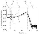
- FIG. 7 shows a SIMS analysis of the substrate 2 ′, the first protective film 3 ′, and the second protective film 4 ′ of the photoelectric conversion element 1 ′ in the thickness direction from the surface of the second protective film 4 ′.
- FIG. 7 is an analysis of the photoelectric conversion element 1 before heating
- 8 is an analysis of the photoelectric conversion element 1 ′ after heating at 700 ° C.
- FIG. 7, 9 is a comparative example, in which only the first protective film 3 is formed by the ALD method.
- the photoelectric conversion element used for the analysis is formed by forming the first protective film 3 with a thickness of 40 nm and the second protective film 4 with a thickness of 20 nm.
- the first protective film 3 is formed by the ALD method
- the second protective film 4 is formed by the sputtering method.
- the photoelectric conversion element of the comparative example is obtained by forming only the first protective film 3 by the ALD method so as to have a film thickness of 40 nm, and then heating similarly.
- the film thicknesses of the first protective film 3 ′ and the second protective film 4 ′ are the film thicknesses set by the apparatus used for the film formation, and are converted in the depth direction by the SIMS analysis shown in FIG. (Axis) does not exactly match. Therefore, in FIG. 7, the interface between the substrate 2 ′ and the first protective film 3 ′ and the interface between the first protective film 3 ′ and the second protective film 4 ′ are 1 ⁇ 2 from the maximum values in the vicinity considered to be near the interface. Was estimated as the interface. In FIG. 7, the dotted line 10 indicates the position estimated as the interface between the substrate 2 'and the first protective film 3', and the dotted line 11 indicates the position estimated as the interface between the first protective film 3 'and the second protective film 4'. In addition, you may estimate each interface using another method.
- the concentration of hydrogen contained in the first protective film 3 ′ was higher than the concentration of hydrogen contained in the second protective film 4 ′.
- the maximum value (2.67E + 22) of the hydrogen concentration contained in the first protective film 3 ′ was present near the substrate 2 ′. Further, the concentration of hydrogen contained in the first protective film 3 ′ is set to a concentration C1 (3.03E + 21) at the boundary with the second protective film 4 ′, and the film thickness of the first protective film 3 is halved.
- C2 (4.01E + 21) and the density C3 (2.67E + 22) at the point showing the maximum value the relationship of (C3-C2)> (C2-C1) was established.
- the minimum value (3.07E + 21) of the concentration of hydrogen contained in the first protective film 3 ′ was more than twice the minimum value (1.38E + 21) of the hydrogen concentration contained in the second protective film 4 ′. .
Abstract
Priority Applications (2)
| Application Number | Priority Date | Filing Date | Title |
|---|---|---|---|
| US14/375,537 US9171972B2 (en) | 2012-01-30 | 2013-01-30 | Method for producing photoelectric converter and phtotelectric converter |
| JP2013556474A JP5762575B2 (ja) | 2012-01-30 | 2013-01-30 | 光電変換素子の製造方法および光電変換素子 |
Applications Claiming Priority (4)
| Application Number | Priority Date | Filing Date | Title |
|---|---|---|---|
| JP2012-017018 | 2012-01-30 | ||
| JP2012017018 | 2012-01-30 | ||
| JP2012145039 | 2012-06-28 | ||
| JP2012-145039 | 2012-06-28 |
Publications (1)
| Publication Number | Publication Date |
|---|---|
| WO2013115275A1 true WO2013115275A1 (fr) | 2013-08-08 |
Family
ID=48905307
Family Applications (1)
| Application Number | Title | Priority Date | Filing Date |
|---|---|---|---|
| PCT/JP2013/052098 WO2013115275A1 (fr) | 2012-01-30 | 2013-01-30 | Procédé de production d'un convertisseur photoélectrique et convertisseur photoélectrique |
Country Status (3)
| Country | Link |
|---|---|
| US (1) | US9171972B2 (fr) |
| JP (1) | JP5762575B2 (fr) |
| WO (1) | WO2013115275A1 (fr) |
Families Citing this family (1)
| Publication number | Priority date | Publication date | Assignee | Title |
|---|---|---|---|---|
| CN220543924U (zh) * | 2023-06-25 | 2024-02-27 | 天合光能股份有限公司 | 太阳能电池、光伏组件和光伏系统 |
Citations (5)
| Publication number | Priority date | Publication date | Assignee | Title |
|---|---|---|---|---|
| JPH07162001A (ja) * | 1993-12-03 | 1995-06-23 | Asahi Glass Co Ltd | 薄膜トランジスタおよびその製造方法 |
| JP2006332510A (ja) * | 2005-05-30 | 2006-12-07 | Kyocera Corp | 太陽電池素子の製造方法 |
| WO2011033826A1 (fr) * | 2009-09-18 | 2011-03-24 | 信越化学工業株式会社 | Cellule solaire, son procédé de fabrication et module de cellule solaire |
| WO2011145731A1 (fr) * | 2010-05-20 | 2011-11-24 | 京セラ株式会社 | Élément de cellule solaire et procédé pour sa production, et module de cellule solaire |
| JP2011249813A (ja) * | 2010-05-21 | 2011-12-08 | Asm Internatl Nv | 太陽電池およびその製造方法 |
Family Cites Families (7)
| Publication number | Priority date | Publication date | Assignee | Title |
|---|---|---|---|---|
| KR101569566B1 (ko) * | 2010-05-04 | 2015-11-16 | 이 아이 듀폰 디 네모아 앤드 캄파니 | 납-텔루륨-리튬-티타늄-산화물을 함유하는 후막 페이스트, 및 반도체 소자의 제조에서의 그의 용도 |
| JP5782768B2 (ja) * | 2011-03-23 | 2015-09-24 | セイコーエプソン株式会社 | 光電変換装置およびその製造方法 |
| US20120255612A1 (en) * | 2011-04-08 | 2012-10-11 | Dieter Pierreux | Ald of metal oxide film using precursor pairs with different oxidants |
| US9209322B2 (en) * | 2011-08-10 | 2015-12-08 | Ascent Solar Technologies, Inc. | Multilayer thin-film back contact system for flexible photovoltaic devices on polymer substrates |
| WO2013123225A1 (fr) * | 2012-02-17 | 2013-08-22 | Applied Materials, Inc. | Empilement de films de passivation pour cellules solaires à base de silicium |
| EP2654085B1 (fr) * | 2012-04-17 | 2017-08-23 | Heraeus Precious Metals North America Conshohocken LLC | Système de réaction inorganique pour composition de pâte électro-conductrice |
| JP5674707B2 (ja) * | 2012-05-22 | 2015-02-25 | 株式会社東芝 | 表示装置 |
-
2013
- 2013-01-30 WO PCT/JP2013/052098 patent/WO2013115275A1/fr active Application Filing
- 2013-01-30 JP JP2013556474A patent/JP5762575B2/ja active Active
- 2013-01-30 US US14/375,537 patent/US9171972B2/en active Active
Patent Citations (5)
| Publication number | Priority date | Publication date | Assignee | Title |
|---|---|---|---|---|
| JPH07162001A (ja) * | 1993-12-03 | 1995-06-23 | Asahi Glass Co Ltd | 薄膜トランジスタおよびその製造方法 |
| JP2006332510A (ja) * | 2005-05-30 | 2006-12-07 | Kyocera Corp | 太陽電池素子の製造方法 |
| WO2011033826A1 (fr) * | 2009-09-18 | 2011-03-24 | 信越化学工業株式会社 | Cellule solaire, son procédé de fabrication et module de cellule solaire |
| WO2011145731A1 (fr) * | 2010-05-20 | 2011-11-24 | 京セラ株式会社 | Élément de cellule solaire et procédé pour sa production, et module de cellule solaire |
| JP2011249813A (ja) * | 2010-05-21 | 2011-12-08 | Asm Internatl Nv | 太陽電池およびその製造方法 |
Non-Patent Citations (1)
| Title |
|---|
| JAN SCHMIDT ET AL.: "INDUSTRIALLY RELEVANT A1203 DEPOSITION TECHNIQUES FOR THE SURFACE PASSIVATION OF Si SOLAR CELLS", 25TH EUROPEAN PHOTOVOLTAIC SOLAR ENERGY CONFERENCE, September 2010 (2010-09-01) * |
Also Published As
| Publication number | Publication date |
|---|---|
| US20150001657A1 (en) | 2015-01-01 |
| JP5762575B2 (ja) | 2015-08-12 |
| JPWO2013115275A1 (ja) | 2015-05-11 |
| US9171972B2 (en) | 2015-10-27 |
Similar Documents
| Publication | Publication Date | Title |
|---|---|---|
| JP6411604B2 (ja) | 太陽電池 | |
| AU2006224719B2 (en) | Photovoltaic cell with thick silicon oxide and silicon nitride passivation fabrication | |
| JP5414298B2 (ja) | 太陽電池の製造方法 | |
| WO2006117980A1 (fr) | Procede de fabrication d’une cellule solaire, cellule solaire et procede de fabrication d’un dispositif semi-conducteur | |
| EP2833391A1 (fr) | Laminat semi-conducteur et procédé de fabrication correspondant, procédé de fabrication de dispositif semi-conducteur, dispositif semi-conducteur, composition de dopant, couche d'injection de dopant, et procédé de réalisation de couche dopée | |
| WO2013095924A1 (fr) | Processus de contact laser, système laser et structures de cellule solaire pour fabrication de cellules solaires ayant des nanoparticules de silicium | |
| WO2015182503A1 (fr) | Élément de cellule solaire, procédé de fabrication de celui-ci et module de cellule solaire | |
| TWI673883B (zh) | 太陽電池元件及太陽電池元件之製造方法 | |
| WO2016047564A1 (fr) | Élément de cellule solaire | |
| Singh et al. | Fabrication of c-Si solar cells using boric acid as a spin-on dopant for back surface field | |
| JP2011166021A (ja) | 太陽電池の製造方法及び太陽電池 | |
| WO2015087472A1 (fr) | Procédé de fabrication de cellules solaires et cellule solaire obtenue par ledit procédé de fabrication | |
| JP5124189B2 (ja) | 光電変換素子の製造方法 | |
| JP2015050277A (ja) | 太陽電池およびその製造方法 | |
| CN111092128A (zh) | 太阳能电池用基板的制造方法及太阳能电池用基板 | |
| TWI489647B (zh) | 製作具有織化表面之半導體層之方法、製作太陽能電池之方法 | |
| JP5762575B2 (ja) | 光電変換素子の製造方法および光電変換素子 | |
| JP2005056875A (ja) | 太陽電池およびその製造方法 | |
| WO2013162024A1 (fr) | Élément de cellule solaire et son procédé de fabrication | |
| JP6139466B2 (ja) | 太陽電池の製造方法 | |
| CN111129217B (zh) | 用于制造太阳能电池的方法和太阳能电池 | |
| CN115101622B (zh) | 一种太阳能电池及其制作方法、光伏组件 | |
| JP4977587B2 (ja) | 太陽電池の製造方法 | |
| JP2007027469A (ja) | 太陽電池素子の製造方法 | |
| US11447869B2 (en) | Manufacturing method for solar cell, solar cell, and solar cell manufacturing apparatus |
Legal Events
| Date | Code | Title | Description |
|---|---|---|---|
| 121 | Ep: the epo has been informed by wipo that ep was designated in this application |
Ref document number: 13743390 Country of ref document: EP Kind code of ref document: A1 |
|
| ENP | Entry into the national phase |
Ref document number: 2013556474 Country of ref document: JP Kind code of ref document: A |
|
| NENP | Non-entry into the national phase |
Ref country code: DE |
|
| WWE | Wipo information: entry into national phase |
Ref document number: 14375537 Country of ref document: US |
|
| 122 | Ep: pct application non-entry in european phase |
Ref document number: 13743390 Country of ref document: EP Kind code of ref document: A1 |