WO2013115136A1 - 表示装置 - Google Patents
表示装置 Download PDFInfo
- Publication number
- WO2013115136A1 WO2013115136A1 PCT/JP2013/051771 JP2013051771W WO2013115136A1 WO 2013115136 A1 WO2013115136 A1 WO 2013115136A1 JP 2013051771 W JP2013051771 W JP 2013051771W WO 2013115136 A1 WO2013115136 A1 WO 2013115136A1
- Authority
- WO
- WIPO (PCT)
- Prior art keywords
- layer
- electrode
- region
- organic
- light
- Prior art date
- Legal status (The legal status is an assumption and is not a legal conclusion. Google has not performed a legal analysis and makes no representation as to the accuracy of the status listed.)
- Ceased
Links
Images





Classifications
-
- H—ELECTRICITY
- H10—SEMICONDUCTOR DEVICES; ELECTRIC SOLID-STATE DEVICES NOT OTHERWISE PROVIDED FOR
- H10K—ORGANIC ELECTRIC SOLID-STATE DEVICES
- H10K59/00—Integrated devices, or assemblies of multiple devices, comprising at least one organic light-emitting element covered by group H10K50/00
- H10K59/10—OLED displays
- H10K59/12—Active-matrix OLED [AMOLED] displays
- H10K59/122—Pixel-defining structures or layers, e.g. banks
-
- H—ELECTRICITY
- H10—SEMICONDUCTOR DEVICES; ELECTRIC SOLID-STATE DEVICES NOT OTHERWISE PROVIDED FOR
- H10K—ORGANIC ELECTRIC SOLID-STATE DEVICES
- H10K50/00—Organic light-emitting devices
- H10K50/80—Constructional details
- H10K50/84—Passivation; Containers; Encapsulations
- H10K50/842—Containers
- H10K50/8426—Peripheral sealing arrangements, e.g. adhesives, sealants
-
- H—ELECTRICITY
- H10—SEMICONDUCTOR DEVICES; ELECTRIC SOLID-STATE DEVICES NOT OTHERWISE PROVIDED FOR
- H10K—ORGANIC ELECTRIC SOLID-STATE DEVICES
- H10K50/00—Organic light-emitting devices
- H10K50/80—Constructional details
- H10K50/85—Arrangements for extracting light from the devices
- H10K50/858—Arrangements for extracting light from the devices comprising refractive means, e.g. lenses
-
- H—ELECTRICITY
- H10—SEMICONDUCTOR DEVICES; ELECTRIC SOLID-STATE DEVICES NOT OTHERWISE PROVIDED FOR
- H10K—ORGANIC ELECTRIC SOLID-STATE DEVICES
- H10K50/00—Organic light-emitting devices
- H10K50/80—Constructional details
- H10K50/86—Arrangements for improving contrast, e.g. preventing reflection of ambient light
-
- H—ELECTRICITY
- H10—SEMICONDUCTOR DEVICES; ELECTRIC SOLID-STATE DEVICES NOT OTHERWISE PROVIDED FOR
- H10K—ORGANIC ELECTRIC SOLID-STATE DEVICES
- H10K59/00—Integrated devices, or assemblies of multiple devices, comprising at least one organic light-emitting element covered by group H10K50/00
- H10K59/80—Constructional details
- H10K59/87—Passivation; Containers; Encapsulations
- H10K59/871—Self-supporting sealing arrangements
- H10K59/8722—Peripheral sealing arrangements, e.g. adhesives, sealants
-
- H—ELECTRICITY
- H10—SEMICONDUCTOR DEVICES; ELECTRIC SOLID-STATE DEVICES NOT OTHERWISE PROVIDED FOR
- H10K—ORGANIC ELECTRIC SOLID-STATE DEVICES
- H10K59/00—Integrated devices, or assemblies of multiple devices, comprising at least one organic light-emitting element covered by group H10K50/00
- H10K59/80—Constructional details
- H10K59/875—Arrangements for extracting light from the devices
- H10K59/879—Arrangements for extracting light from the devices comprising refractive means, e.g. lenses
-
- H—ELECTRICITY
- H10—SEMICONDUCTOR DEVICES; ELECTRIC SOLID-STATE DEVICES NOT OTHERWISE PROVIDED FOR
- H10K—ORGANIC ELECTRIC SOLID-STATE DEVICES
- H10K59/00—Integrated devices, or assemblies of multiple devices, comprising at least one organic light-emitting element covered by group H10K50/00
- H10K59/80—Constructional details
- H10K59/8791—Arrangements for improving contrast, e.g. preventing reflection of ambient light
-
- H—ELECTRICITY
- H10—SEMICONDUCTOR DEVICES; ELECTRIC SOLID-STATE DEVICES NOT OTHERWISE PROVIDED FOR
- H10K—ORGANIC ELECTRIC SOLID-STATE DEVICES
- H10K2102/00—Constructional details relating to the organic devices covered by this subclass
- H10K2102/301—Details of OLEDs
- H10K2102/302—Details of OLEDs of OLED structures
- H10K2102/3023—Direction of light emission
- H10K2102/3026—Top emission
-
- H—ELECTRICITY
- H10—SEMICONDUCTOR DEVICES; ELECTRIC SOLID-STATE DEVICES NOT OTHERWISE PROVIDED FOR
- H10K—ORGANIC ELECTRIC SOLID-STATE DEVICES
- H10K50/00—Organic light-emitting devices
- H10K50/80—Constructional details
- H10K50/85—Arrangements for extracting light from the devices
- H10K50/852—Arrangements for extracting light from the devices comprising a resonant cavity structure, e.g. Bragg reflector pair
-
- H—ELECTRICITY
- H10—SEMICONDUCTOR DEVICES; ELECTRIC SOLID-STATE DEVICES NOT OTHERWISE PROVIDED FOR
- H10K—ORGANIC ELECTRIC SOLID-STATE DEVICES
- H10K50/00—Organic light-emitting devices
- H10K50/80—Constructional details
- H10K50/86—Arrangements for improving contrast, e.g. preventing reflection of ambient light
- H10K50/865—Arrangements for improving contrast, e.g. preventing reflection of ambient light comprising light absorbing layers, e.g. light-blocking layers
-
- H—ELECTRICITY
- H10—SEMICONDUCTOR DEVICES; ELECTRIC SOLID-STATE DEVICES NOT OTHERWISE PROVIDED FOR
- H10K—ORGANIC ELECTRIC SOLID-STATE DEVICES
- H10K59/00—Integrated devices, or assemblies of multiple devices, comprising at least one organic light-emitting element covered by group H10K50/00
- H10K59/30—Devices specially adapted for multicolour light emission
- H10K59/38—Devices specially adapted for multicolour light emission comprising colour filters or colour changing media [CCM]
-
- H—ELECTRICITY
- H10—SEMICONDUCTOR DEVICES; ELECTRIC SOLID-STATE DEVICES NOT OTHERWISE PROVIDED FOR
- H10K—ORGANIC ELECTRIC SOLID-STATE DEVICES
- H10K59/00—Integrated devices, or assemblies of multiple devices, comprising at least one organic light-emitting element covered by group H10K50/00
- H10K59/80—Constructional details
- H10K59/875—Arrangements for extracting light from the devices
- H10K59/876—Arrangements for extracting light from the devices comprising a resonant cavity structure, e.g. Bragg reflector pair
Definitions
- the present invention relates to an organic EL display device.
- an organic EL (Electro luminescence) display device is excellent as an excellent flat panel display because it can realize low power consumption, thinning, and high image quality. Has attracted attention.
- the organic EL display device has a problem that the external light reflectance is high, and the contrast is lowered when used at the window or outdoors.
- the organic EL display device that performs full-color display is roughly divided into a method that performs full-color display using an EL layer that emits red, green, and blue (painting method), and an EL layer that emits white.
- a full color display method using color filters that transmit red, green, and blue light can be cited as an example.
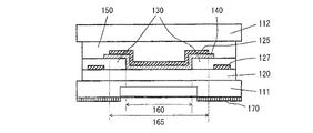
- Patent Document 1 As shown in FIG. 11, a transparent first support 111, a first electrode 120, an organic EL layer 140, a second electrode 125, and a second support 112 are provided.
- the insulating layers 130 are provided so as to be stacked in this order, and have a light emitting region opened between the first electrode 120 and the second electrode 125 so as to cover the non-light emitting region.
- 1 describes a light-emitting organic EL display panel in which one support 111 side is a light emission extraction side.
- a visual suppression layer 170 is provided.
- Patent Document 2 describes a display device that can prevent a decrease in contrast due to reflection of external light by providing a light absorption layer on an insulating film between openings serving as light emitting portions.
- Patent Document 3 includes an elliptically polarizing plate that can compensate for a broadband wavelength region in visible light, thereby preventing reflection of external light in the broadband wavelength region in a metal electrode incorporated in an organic EL device or the like. It is stated that you can.
- Japanese Patent Publication Japanese Patent Laid-Open No. 2008-277270 (published on November 13, 2008)” Japanese Patent Publication “Japanese Unexamined Patent Publication No. 2003-17272 (published on January 17, 2003)” Japanese Patent Publication “Japanese Patent Laid-Open No. 2004-226842 (published on August 12, 2004)”
- the visual suppression layer 170 is patterned to have a wider opening than the light emitting region 160 in order to ensure a high aperture ratio.
- the visual suppression layer 170 is formed to have an opening wider than the light emitting region 160, there is a region outside the light emitting region 160 where the visual suppression layer 170 is not formed. In such a region, external light reflection occurs, and as a result, there is a problem that the contrast of the light-emitting organic EL display panel is lowered.
- Patent Document 2 As in the case of Patent Document 1, since the light absorption layer is formed so as to have an opening wider than the light emitting portion, the light absorbing layer is formed outside the light emitting portion. In such a region, external light reflection occurs, and as a result, there is a problem that the contrast of the display device is lowered.
- Patent Document 3 in addition to the use of a circularly polarizing plate, the luminous efficiency is reduced to about 40%, and in addition, an elliptically polarizing plate that can compensate for a relatively expensive broadband wavelength region in visible light. Therefore, the manufacturing unit price of the display device is increased.
- the black matrix (BM) 221 is formed so as to cover a part of the light emitting portion in consideration of the bonding margin as shown in FIG.
- the organic EL display device 200 can be considered, the opening of the organic EL display device 200 is remarkably lowered, and the display image quality is lowered.
- the TFT 211 As shown in the drawing, on the support substrate 210, the TFT 211, the signal line 212, the interlayer insulating film 213, the first electrode 214, and the organic EL element forming layer at the edge of the first electrode 214 are formed.
- An edge cover 215 which is an insulating layer for preventing the first electrode 214 and the second electrode 219 from being short-circuited due to thinning or electric field concentration is provided.
- a hole injection layer and a hole transport layer 216 are formed on the support substrate 210 so as to cover the edge cover 215 and the surface of the first electrode 214 exposed by the opening of the edge cover 215, and a light emitting layer. 217, an electron transport layer and electron injection layer 218, and a second electrode 219 are sequentially stacked.
- An organic EL element including the first electrode 214, the hole injection layer and hole transport layer 216, the light emitting layer 217, the electron transport layer and electron injection layer 218, and the second electrode 219 has a low voltage.
- the light-emitting element emits white (W) light and can emit high luminance light by direct current drive.
- a black matrix (BM) 221 and color filters 222R, 222G, and 222B are provided on the surface of the sealing substrate 220 that faces the support substrate 210.
- the two substrates 210 and 220 are formed such that the black matrix (BM) 221 covers a part of the light emitting portion for the bonding margin, and the light extraction portion is narrowed.
- the display image quality of the EL display device 200 is degraded.
- the opening of the black matrix (BM) 221 is made larger than the light emitting portion in order to prevent the light extraction portion from becoming narrow and the display image quality of the organic EL display device 200a from deteriorating.
- the black matrix (BM) 221 is not formed outside the light-emitting portion, as in the configurations of Patent Documents 1 and 2. In such a region, external light reflection occurs, and as a result, the contrast of the display device is lowered.
- FIG. 14 is a diagram showing a schematic configuration of an organic EL display device 250 formed by a separate coating method using an edge cover material containing carbon black.
- a TFT 252 As shown in the figure, on the substrate 251, a TFT 252, an interlayer insulating film 253, an edge cover 255 containing the first electrode 254 and carbon black are formed.
- a hole injection layer and a hole transport layer 256 are formed so as to cover the first electrode 254 and the edge cover 255, and are regions between the edge covers 255, and the hole injection layer and the hole transport layer 256.
- light-emitting layers 257R, 257G, and 257B that emit red, green, and blue light formed by a separate coating method are formed.
- an electron transport layer and an electron injection layer (not shown) and a second electrode 258 are formed so as to cover the hole injection layer and the hole transport layer 256 and the light emitting layers 257R, 257G, and 257B. Yes.
- the present invention has been made in view of the above problems, and an object of the present invention is to provide a display device capable of suppressing a decrease in contrast.
- the display device of the present invention is a display device in which a plurality of picture elements are arranged in a matrix, and each of the picture elements includes a first region and the first And a second region formed around one region, wherein the first region is a display region, and the second region is different in that reflected light is reduced by optical interference.
- a laminated film including a plurality of layers having a refractive index is provided.
- the second region is provided with the laminated film including a plurality of layers having different refractive indexes, which reduces reflected light by optical interference, thereby realizing a display device with high contrast. be able to.
- each of the picture elements includes the first region and the second region formed around the first region.
- the first region is a display region
- the second region is provided with a laminated film composed of a plurality of layers having different refractive indexes that reduces reflected light by optical interference.
- FIG. It is sectional drawing which shows schematic structure of the organic electroluminescent display apparatus of other one Embodiment of this invention. It is a figure for demonstrating the optical interference layer (laminated film) formed in EC area
- FIG. It is a figure which shows schematic structure of the organic electroluminescent display apparatus of other one Embodiment of this invention. It is a figure which shows the different structure which the organic electroluminescent display apparatus of other one embodiment of this invention can take. It is a figure which shows schematic structure of the light emission type organic electroluminescent display panel of patent document 1.
- FIG. It is a figure which shows schematic structure of the conventional organic electroluminescence display of the system which carries out a full color display using the EL layer which light-emits white, and the color filter which permeate
- BM black matrix
- FIG. 2 is a cross-sectional view illustrating a schematic configuration of the organic EL display device 1.
- the organic EL display device 1 includes a support substrate 10, a sealing substrate 14 disposed to face the support substrate 10, and a sealing resin for bonding the support substrate 10 and the sealing substrate 14 together. 15.
- the region surrounded by the sealing resin 15 and sandwiched between the support substrate 10 and the sealing substrate 14 is hollow, but a filling resin or the like is formed in this portion. You can also.
- the organic EL display device 1 is of a top emission type in which light emitted on the support substrate 10 is emitted as emitted light through the sealing substrate 14.
- a full color image display is realized by using a light emitting layer whose emission color is white (W) and introducing a microcavity structure described later.
- the spectrum of the light emitted from the organic EL layer can be adjusted by the color filter layer.
- the white (W) light emitting layer is composed of a plurality of light emitting layers of different colors, and W light emission is obtained by superimposing these light emitting colors.
- Examples of the combination of the emission colors include a combination of blue light and yellow (more preferably yellow (orange) having a peak intensity in green and red) light, a combination of blue light and yellow light, and the like.
- examples of the combination of the emission colors include a combination of red light, blue light, and green light.
- FIG. 1 is a partially enlarged view in which the G picture element portion is enlarged in the organic EL display device 1 in which each pixel composed of three R, G, B picture elements is arranged in a matrix.
- the supporting substrate 10 includes an insulating substrate 2, a TFT element 3, a signal line 4, an interlayer insulating film 5, and a TFT element 3 via a contact hole formed in the interlayer insulating film 5.
- the first electrode 6 electrically connected to the drain electrode of the first electrode 6, and the organic layer 8 becomes thin or the electric field concentration occurs at the edge of the first electrode 6.
- the edge cover 7 which is an insulating layer for preventing the electrode 9 from being short-circuited, and the edge cover 7 and the surface of the first electrode 6 exposed by the opening of the edge cover 7 are formed to be covered.
- An organic layer 8 in which a hole injection layer, a hole transport layer, a light emitting layer, an electron transport layer, and an electron injection layer are sequentially stacked, and a second electrode 9 are provided.
- the region where the first electrode 6, the organic layer 8, and the second electrode 9 are in direct contact with each other becomes a light emitting region (first region), and the edge cover 7 is formed.
- the non-light-emitting area that is set becomes the EC area (second area).
- the first electrode 6 is a layer having a function of injecting (supplying) holes into the organic layer 8. That is, in the present embodiment, the first electrode 6 is an anode.
- the first electrode 6 is connected to the TFT element 3 through a contact hole as shown in FIG.
- the first electrode 6 is formed in a pattern corresponding to each pixel by photolithography and etching after an electrode material is formed by a sputtering method or the like.
- the 1st electrode 6 can be laminated
- CVD Chemical vapor deposition, chemical vapor deposition
- the first electrode 6 a metal material having a high reflectance can be used.
- the material constituting the first electrode 6 include Ag or an Ag alloy, Al or an Al alloy, and the like.
- the first electrode 6 As described above, by forming the first electrode 6 from a material having high reflectance, the light emitted from the organic layer 8 can be efficiently emitted through the sealing substrate 14.
- the refractive index is lower than the acrylic resin (refractive index: 1.58) or polyimide material (refractive index: 1.63) conventionally used as the edge cover material. 1.3 to 1.4) An acrylic resin is used as the edge cover 7.
- Examples of the material of the hole injection layer, the hole transport layer, or the hole injection layer and the hole transport layer in the organic layer 8 include anthracene, azatriphenylene, fluorenone, hydrazone, stilbene, triphenylene, benzine, and styrylamine. , Triphenylamine, porphyrin, triazole, imidazole, oxadiazole, oxazole, polyarylalkane, phenylenediamine, arylamine, and derivatives thereof, thiophene compounds, polysilane compounds, vinylcarbazole compounds, aniline compounds, etc. A linear or heterocyclic conjugated monomer, oligomer, polymer, or the like can be used.
- the light emitting layer in the organic layer 8 is formed of a material having high luminous efficiency such as a low molecular fluorescent dye or a metal complex.
- a material having high luminous efficiency such as a low molecular fluorescent dye or a metal complex.
- the material of the electron transport layer, the electron injection layer, or the electron transport layer and the electron injection layer in the organic layer 8 for example, tris (8-quinolinolato) aluminum complex, oxadiazole derivative, triazole derivative, phenylquinoxaline derivative, Examples include silole derivatives.
- NPB hole transport layer
- Alq3 reffractive index: 1.71
- BCP reffractive index: is used as the electron transport layer. 1.71) were used, but not limited thereto.
- CBP reffractive index: 1.77
- F8BT reffractive index: 1.8
- DOO-MEH-PPV were used as these layers.
- P3HT-PCBM reffractive index: 2.10
- sDPVB sDPVB
- PFO refractive index: 1.73
- layers other than the light emitting layer in the organic layer 8 are not essential layers, and may be appropriately formed according to required characteristics of the organic EL element.
- a material which comprises the 2nd electrode 9 transparent, such as ITO (Indium Tin Oxide: Indium tin oxide), IZO (Indium Zinc Oxide: Indium zinc oxide), a gallium addition zinc oxide (GZO), etc., for example.
- ITO Indium Tin Oxide: Indium tin oxide
- IZO Indium Zinc Oxide: Indium zinc oxide
- GZO gallium addition zinc oxide
- a conductive material, a metal material such as gold (Au), nickel (Ni), platinum (Pt), or a laminated film thereof can be used.
- Examples of the method for laminating the second electrode 9 include sputtering, vacuum deposition, CVD (chemical vapor deposition), plasma CVD, and printing.
- the sealing substrate 14 includes a transparent substrate 11 and a black matrix (BM) 12 and a color filter 13G on the surface of the transparent substrate 11 facing the support substrate 10.
- BM black matrix
- the light extraction portion becomes narrow, and the opening portion of the black matrix (BM) 12 is suppressed in order to suppress the deterioration of the display image quality of the organic EL display device 1.
- BM black matrix
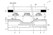
- FIG. 3 is a diagram for explaining an optical interference layer (laminated film) formed in the EC region (second region) of the organic EL display device 1.
- an EC region (second region) of the organic EL display device 1 includes an edge cover 7 made of a low refractive index (1.3 to 1.4) acrylic resin, a hole transport layer, and the like.
- NPB refractive index: 1.8
- Alq3 refractive index: 1.71
- BCP refrtive index: 1.71
- An optical interference layer in which the second electrode 9 made of the semi-transmissive film is laminated is provided.
- the light reflected by the second electrode 9 and the light reflected by the interface between the edge cover 7 and the organic layer 8 are interfered and have an antireflection effect.
- a black matrix (BM) 12 is formed in a part of the EC region (second region), and there is a region where the black matrix (BM) 12 is not formed in the EC region (second region).
- BM black matrix
- each layer of the optical interference layer transmits part of light in a predetermined wavelength range (for example, light having a wavelength of 550 nm). Even if the light emitting region (first region) is formed, the light emitting region (first region) which is the display region is not narrowed, so that the image quality of the organic EL display device 1 is not deteriorated. .
- the organic EL display device 1 since the optical interference layer does not need to contain carbon black, the organic EL display device 1 with high reliability can be realized.
- the layer 8 is preferably formed with a thickness satisfying the following formula (1).
- d ⁇ / (4 ⁇ n1)
- Formula (1) d represents the film thickness of the organic layer 8
- ⁇ represents an arbitrary wavelength at which reflected light is desired to be suppressed
- n 1 represents the refractive index of the organic layer 8.
- NPB hole transport layer
- Alq3 reffractive index: 1.71
- BCP reffractive index: 1.1.7
- 71 is used, but only one or two layers selected from the layers constituting the organic layer 8 may be formed in the EC region (second region).
- the optical interference layer is formed in the EC region (second region) using the material used in the light emitting region (first region) of the organic EL display device 1.
- the present invention is not limited to this, and an optical interference layer can be formed in the EC region (second region) using a material that is not used in the light emitting region (first region) of the organic EL display device 1.
- an optical interference layer may be provided so as to satisfy the following formula (2) and the following formula (3).
- ⁇ represents an arbitrary wavelength for which reflected light is desired to be suppressed
- the film thickness of the lower layer (corresponding to the organic layer 8) in contact with the second electrode 9 may be obtained from the above formula (3).
- microcavity structure demonstrated in detail below is employ
- the light emitting region (first region) of the organic EL display device 1 since the light emitting region (first region) of the organic EL display device 1 has a microcavity structure, not only the EC region (second region) but also the light emitting region (first region). ), The reflection of external light can be suppressed, and the organic EL display device 1 with high contrast can be realized.
- FIG. 4 is a diagram for explaining the effect of preventing reflection of external light by the microcavity structure.
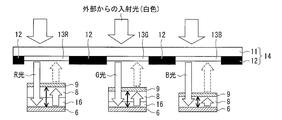
- the color filters 13R, 13G, and 13B provided in the openings of the black matrix (BM) 12 are each provided with a first electrode 6, an organic layer 8, and a second electrode 9. Light emitted from the EL element can be transmitted to the outside, and incident light from the outside is caused to enter each of the organic EL elements.
- the reflected light of the incident light from the outside in each of the organic EL elements is mixed with the light emitted from each of the organic EL elements and is emitted to the outside, resulting in a decrease in color purity, a decrease in contrast and a decrease in visibility.
- the incident light from the outside is white light
- the incident light from the outside passes through the color filter 13R and becomes R light
- the organic EL element of the red picture element provided under the color filter 13R Is incident on.
- the distance between the first electrode 6 and the second electrode 9 of the organic EL element of the red picture element resonates with the peak wavelength of red light. It is the optical path length.
- the distance between the first electrode 6 and the second electrode 9 of the organic EL element of the green picture element is an optical path length at which the peak wavelength of green light resonates.
- the distance between the first electrode 6 and the second electrode 9 of the blue pixel organic EL element is an optical path length at which the peak wavelength of blue light resonates.
- the organic EL element having red and green picture elements for example, ITO, IZO, or gallium-added oxidation is provided between the first electrode 6 and the organic layer 8 in order to adjust the length of the optical path length.
- Such an organic EL display device 1 can obtain outgoing light with high color purity and suppress reflection of external light incident between the first electrode 6 and the second electrode 9, so that the contrast is high. Visibility can be improved.
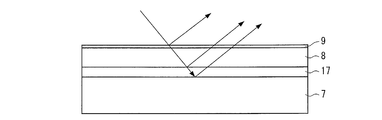
- FIG. 5 is a diagram showing an example of an optical interference layer that can be provided in the EC region (second region) in the organic EL display device 1 in which the microcavity structure is adopted in the light emitting region (first region). It is.
- a transparent electrode layer 16 made of a transparent conductive material such as IZO or gallium-doped zinc oxide (GZO) is formed.
- a layer 17 made of the same layer of the same material as the transparent electrode layer 16 is inserted between the edge cover 7 and the organic layer 8 as shown.
- the optical interference effect by the multilayer film can be obtained from the optical interference layer shown in FIG.
- FIG. 6 a second embodiment of the present invention will be described based on FIG. 6 and FIG.
- the present embodiment it is formed of a material having a refractive index substantially equal to the refractive index of the organic layer 8 between the organic layer 8 and the second electrode 9 in the EC region (second region), and
- an optical path adjusting layer 18 that transmits part of light in a predetermined wavelength range is provided.
- Other configurations are as described in the first embodiment.
- members having the same functions as those shown in the drawings of the first embodiment are given the same reference numerals, and descriptions thereof are omitted.
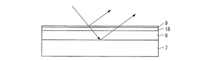
- FIG. 6 is a cross-sectional view showing a schematic configuration of the organic EL display device 1a.
- the EC region (second region) of the support substrate 10a of the organic EL display device 1a has a refractive index substantially equal to that of the organic layer 8 between the organic layer 8 and the second electrode 9.
- An optical path adjusting layer 18 that is formed of a material having an equal refractive index, preferably the same refractive index, and transmits a part of light in a predetermined wavelength range is provided.
- FIG. 7 is a diagram for explaining an optical interference layer (laminated film) formed in the EC region (second region) of the organic EL display device 1a.
- the film thickness of the organic layer 8 is relatively difficult to change. Instead of changing, the film thickness of the optical path adjusting layer 18 can be changed, and the light in the predetermined wavelength range reflected on the surface and interface of each layer of the optical interference layer can be made to interfere.
- Embodiment 3 a third embodiment of the present invention will be described with reference to FIG.
- the present embodiment is different from the first and second embodiments in that an optical interference layer is provided in the EC region (second region) of the organic EL display device 20 formed by a separate coating method.
- Other configurations are as described in the first embodiment.
- members having the same functions as those shown in the drawings of Embodiments 1 and 2 are given the same reference numerals, and descriptions thereof are omitted.
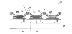
- FIG. 8 is a diagram showing a schematic configuration of the organic EL display device 20 formed by a separate coating method.
- a TFT 22 As shown in the figure, a TFT 22, an interlayer insulating film 23, a first electrode 24, and an edge cover 25 are formed on the substrate 21.
- a hole injection layer and a hole transport layer 26 are formed so as to cover the first electrode 24 and the edge cover 25, and are regions between the edge covers 25, the hole injection layer and the hole transport layer 26.
- light-emitting layers 27R, 27G, and 27B that emit red, green, and blue light formed by a separate coating method are formed.
- an electron transport layer (not shown) and a second electrode 28 are formed so as to cover the hole transport layer 26 and the light emitting layers 27R, 27G, and 27B.
- the light emitting layers 27R, 27G, and 27B having different thicknesses are formed in the respective first regions provided in the respective picture elements constituting one pixel.
- a hole injection layer and a hole transport layer 26 and an electron transport layer are provided in the second region where the edge cover 25 is formed.
- the present invention is not limited to this, and the light emitting layers 27R, 27G, and 27B may be provided up to the second region where the edge cover 25 is formed.
- the second regions are the light emitting layers 27R, 27G formed in the first regions of adjacent picture elements.
- Layers 27R, 27G, and 27B and an electron transport layer are formed.
- the refractive index is lower than that of acrylic resin (refractive index: 1.58) or polyimide-based material (refractive index: 1.63), which has been conventionally used as an edge cover material.
- a rate (1.3 to 1.4) acrylic resin is used as the edge cover 25.
- NPB hole transport layer
- BCP reffractive index: 1.71
- the EC region (second region) of the organic EL display device 20 includes an edge cover 25 made of a low refractive index (1.3 to 1.4) acrylic resin, a hole, NPB (refractive index: 1.8) as a transport layer, BCP (refractive index: 1.71) as an electron transport layer (not shown), and a second electrode 28 made of a semi-transmissive film formed of a thin film. And an optical interference layer laminated.
- an optical interference layer including the light emitting layers 27R, 27G, and 27B can be formed in the second region.
- Embodiment 4 Next, a fourth embodiment of the present invention will be described based on FIGS.
- a second electrode 9 In the EC region (second region) of the organic EL display device 1b having the sealing substrate 14 provided with the color filter used in the first and second embodiments, a second electrode 9, an insulating layer 19, The difference from Embodiments 1 and 2 is that an optical interference layer comprising a sealing resin material 29 or an air layer is provided.
- Other configurations are as described in the first embodiment.
- members having the same functions as those shown in the drawings of Embodiments 1 and 2 are given the same reference numerals, and descriptions thereof are omitted.
- FIG. 9 is a diagram showing a schematic configuration of the organic EL display device 1b.
- the refractive index of the sealing resin material 29, which will be described later, is on the second electrode 9.
- An insulating layer 19 made of a larger acrylic resin is provided.
- a sealing resin material 29 made of a system resin is provided.
- the refractive index of the sealing resin material 29 is not limited to this, and may be smaller than the refractive index of the insulating layer 19.
- the optical interference layer including the second electrode 9, the insulating layer 19, and the sealing resin material 29 is provided in the EC region (second region) of the organic EL display device 1b. ing.
- the reflected light at the interface between the sealing resin material 29 and the insulating layer 19 the reflected light at the surface of the second electrode 9, and Interferes with each other and has an antireflection effect.
- an optical path length can be set comparatively freely. I can do it.
- a sealing film inorganic film as a barrier layer, or the like can also be used.
- the sealing resin material 29 is a filling resin layer having a moisture absorption effect that is formed between the support substrate 10b and the sealing substrate 14.
- acrylic resin (refractive index: 1.58), polyimide material (refractive index: 1.63), low refractive index (1.3 To 1.4) Any acrylic resin can be used.
- FIG. 10 is a diagram showing a schematic configuration of the organic EL display device 1c.
- an insulating layer 19 made of acrylic resin is provided on the second electrode 9 in the EC region (second region) of the support substrate 10b of the organic EL display device 1c.
- an air layer having a refractive index of 1 is formed between the support substrate 10b and the sealing substrate 14 instead of the sealing resin material 29 shown in FIG.
- the reflected light at the interface between the air layer and the insulating layer 19 and the reflected light at the surface of the second electrode 9 are interfered with each other. Has antireflection effect.
- an optical path length can be set comparatively freely. I can do it.
- a sealing film inorganic film as a barrier layer, or the like can also be used.
- the laminated film provided in the second region of the display device of the present invention includes a first layer and a refractive index of the first layer so as to be in contact with the first layer on the first layer.
- a second layer formed of a material having a higher refractive index and a third layer having a refractive index different from that of the second layer formed on the second layer so as to be in contact with the second layer. And a layer.
- the first region of the display device of the present invention includes a first electrode as a lower layer, a second electrode as an upper layer disposed opposite to the first electrode, the first electrode, and the first electrode. And an organic layer in which a plurality of layers emitting light provided between the two electrodes are stacked, and the second region covers an end portion of the adjacent first electrode.
- the first layer is the first insulating layer
- the second layer is at least one of the organic layers
- the third layer is the formation of the second electrode. It may be a layer.
- the stacked film (optical interference layer) can be formed in the second region using the layer formed in the first region which is the display region, the second Even if the laminated film (optical interference layer) is provided in the region, the number of manufacturing steps of the display device does not increase.
- the refractive index of at least one layer in the organic layer is substantially equal between at least one layer in the organic layer and the formation layer of the second electrode. It is preferable that an optical path adjusting layer formed of a material having a refractive index is provided.
- the film thickness of the optical path adjustment layer is changed.
- the light of the predetermined wavelength range reflected by the surface and interface of each layer of the laminated film can be made to interfere.
- the multilayer film provided in the second region of the display device of the present invention is formed on the first layer so as to be in contact with the first layer, which reflects part of light.
- a third layer formed of a material having a refractive index smaller than that of the second layer so as to be in contact with the second layer on the second layer. It may be.
- the optical interference effect can be used to suppress light reflection in the second region.
- the first region of the display device of the present invention includes a first electrode as a lower layer, a second electrode as an upper layer disposed opposite to the first electrode, the first electrode, and the first electrode. And an organic layer in which a plurality of layers emitting light provided between the two electrodes are stacked, and the second region covers an end portion of the adjacent first electrode.
- a laminated film can be provided by the second electrode formation layer, the second insulating layer (or organic layer), and the air layer.
- the first region of the display device of the present invention includes a first electrode as a lower layer, a second electrode as an upper layer disposed opposite to the first electrode, the first electrode, and the first electrode. And an organic layer in which a plurality of layers emitting light provided between the two electrodes are stacked, and the second region covers an end portion of the adjacent first electrode.
- the organic layer is provided with a sealing resin layer, the first layer is a formation layer of the second electrode, and the second layer A said second insulation layer (or organic layer), the third layer may be the sealing resin layer.
- a laminated film can be provided by the second electrode formation layer, the second insulating layer (or organic layer), and the sealing resin layer.
- each color filter layer that selectively transmits light in different predetermined wavelength ranges is provided.
- the light in the predetermined wavelength range emitted from the first region may be light obtained by emitting white light emitted from the organic layer through each color filter layer.
- the organic layer that emits the white light can be provided in all the pixels of the display device. Therefore, the first region and the second region can be provided.
- the organic layer that emits the white light can be provided on the entire surface including the above.
- a laminated film (optical interference layer) including the organic layer that emits the white light can be provided.
- the light emitting layer in the organic layer may be formed of a material that emits light in a different predetermined wavelength range for each pixel constituting one pixel.
- a light emitting layer made of a material that emits light having a different predetermined wavelength range is generally formed for each picture element constituting one pixel by a painting method.
- a light emitting layer having a different thickness is formed for each element.
- the distance between the first electrode and the second electrode is the color filter layer. It is preferable that the peak wavelength of the light that is transmitted through the optical path length is resonating.
- the distance between the first electrode and the second electrode is an optical path length at which the peak wavelength of the light transmitted through the color filter layer resonates. Since the microcavity structure is used, external light reflection can be suppressed not only in the second region but also in the first region, and a display device with high contrast is realized. be able to.
- a part of the second region in the display device of the present invention may be provided with a light shielding film.
- the present invention can be suitably used for a display device such as an organic EL display device.
- Second electrode 10 1, 1a, 1b, 1c Organic EL display device (display device) 2, 21 Insulating substrate 3, 22 TFT element 4 Signal line 5, 23 Interlayer insulating film 6, 24 First electrode 7, 25 Edge cover 8 Organic layer 9 Second electrode 10, 10a, 10b Support substrate 11 Transparent substrate 12 Black matrix (shading layer) 13R / 13G / 13B Color filter 14 Sealing substrate 15 Sealing resin 16 Transparent electrode layer 17 Same layer as transparent electrode layer 18 Optical path adjusting layer 19 Insulating layer 20 Organic EL display device (display device) 24 First electrode 25 Edge cover 26 Hole injection layer and hole transport layer 27R / 27G / 27B Light emitting layer 28 Second electrode 29 Sealing resin material
Landscapes
- Physics & Mathematics (AREA)
- Optics & Photonics (AREA)
- Engineering & Computer Science (AREA)
- Microelectronics & Electronic Packaging (AREA)
- Electroluminescent Light Sources (AREA)
Abstract
有機EL表示装置(1)のEC領域(第2の領域)には、低屈折率アクリル系樹脂からなるエッジカバー(7)と、有機層(8)と、薄膜で形成された半透過膜からなる第2の電極(9)と、が積層された光学干渉層が備えられているので、表示領域を狭くすることなく、コントラストの低下を抑制でき、かつ、信頼性の高い有機EL表示装置を実現できる。
Description
本発明は有機EL表示装置に関するものである。
近年、さまざまなフラットパネルディスプレイが開発されており、特に、有機EL(Electro luminescence)表示装置は、低消費電力化、薄型化および高画質化などを実現できる点から、優れたフラットパネルディスプレイとして高い注目を浴びている。
しかしながら、有機EL表示装置は、外光反射率が高く、窓際や野外での使用時にコントラストが低下するという問題がある。
フルカラー表示を行う有機EL表示装置の方式としては、大きく分けて、赤色、緑色、及び青色を発光するEL層を用いてフルカラー表示を行う方式(塗り分け方式)と、白色を発光するEL層と赤色、緑色、及び青色の光を透過するカラーフィルタとを用いてフルカラー表示する方式とを例に挙げることができる。
このような有機EL表示装置の分野においては、特に、高コントラスト化を実現するためのさまざまな構造が検討されている。
特許文献1には、図11に図示されているように、透明な第1の支持体111、第1の電極120、有機EL層140、第2の電極125および第2の支持体112を、この順に積層し、且つ、第1の電極120と第2の電極125との間に、発光領域を開口し、非発光領域を覆うように、区画された絶縁層130が備えられており、第1の支持体111側を発光取り出し側とする発光型有機EL表示パネルについて記載されている。
そして、上記発光型有機EL表示パネルには、第2の電極125、補助電極127および有機EL層140の一つ以上と、これらの周囲との、反射率の差や色合いの差による視認を抑制するための視認抑制層170が設けられている。
このような構成によれば、第2の電極125、補助電極127および有機EL層140と、これらの周囲との、反射率の差や色合いの差に起因した不要な視認を抑制することができると記載されている。
特許文献2には、発光部となる開口部間の絶縁膜上に光吸収層を設けることにより、外光反射によるコントラストの低下を防止できる表示装置について記載されている。
また、特許文献3には、可視光における広帯域波長領域を補償できる楕円偏光板を備えることにより、有機EL装置などに組み込まれている金属電極において、広帯域波長領域の外部光の反射を防止することができると記載されている。
上記特許文献1の図11に図示されている構成においては、高い開口率を確保するため、視認抑制層170は、発光領域160よりは広い開口部を有するようにパターニングされている。
しかしながら、上記構成においては、視認抑制層170が発光領域160より広い開口部を有するように形成されているため、発光領域160外であって、視認抑制層170が形成されてない領域が存在し、このような領域においては、外光反射は生じてしまい、結果として、発光型有機EL表示パネルのコントラストの低下を招いてしまうという問題がある。
また、上記特許文献2においても、上記特許文献1の場合と同様に、光吸収層が発光部より広い開口部を有するように形成されているため、発光部外に、光吸収層が形成されてない領域が存在し、このような領域においては、外光反射は生じてしまい、結果として、表示装置のコントラストの低下を招いてしまうという問題がある。
また、上記特許文献3の構成においては、円偏光板を用いるために発光効率が40%程度に低下することに加え、別途、比較的高価である可視光における広帯域波長領域を補償できる楕円偏光板を備える必要が生じるため、表示装置の製造単価の上昇を招いてしまう。
一方、上記特許文献1および2における問題を解決するため、図12に図示されているように、張り合わせマージンを考慮し、ブラックマトリクス(BM)221が発光部の一部を覆うように形成された有機EL表示装置200とすることも考えられるが、有機EL表示装置200の開口部が著しく低下してしまい、表示画質の低下を招いてしまう。
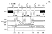
以下、図12に基づいて、白色を発光するEL層と赤色、緑色、及び青色の光を透過するカラーフィルタとを用いてフルカラー表示する方式の有機EL表示装置200の概略的な構成について説明する。
図示されているように、支持基板210上には、TFT211と、信号線212と、層間絶縁膜213と、第1の電極214と、第1の電極214のエッジで有機EL素子の形成層が薄くなったり電界集中が起こったりすることで、第1の電極214と第2の電極219とが短絡することを防止するための絶縁層であるエッジカバー215と、が備えられている。
そして、支持基板210上には、エッジカバー215およびエッジカバー215の開口部によって露出している第1の電極214の表面を覆うように、正孔注入層および正孔輸送層216と、発光層217と、電子輸送層および電子注入層218と、第2の電極219と、が順に積層されている。
第1の電極214と、正孔注入層および正孔輸送層216と、発光層217と、電子輸送層および電子注入層218と、第2の電極219と、からなる有機EL素子は、低電圧直流駆動による高輝度発光が可能であり、白色(W)光を発光する発光素子である。
一方、封止基板220における上記支持基板210と対向する面側には、ブラックマトリクス(BM)221とカラーフィルタ222R・222G・222Bとが備えられている。
そして、有機EL表示装置200においては、上記両基板210・220は張り合わせマージン分、ブラックマトリクス(BM)221が発光部の一部を覆うように形成され、光取り出し部が狭くなってしまい、有機EL表示装置200の表示画質の低下を招いてしまう。
図13に示す有機EL表示装置200aにおいては、光取り出し部が狭くなり、有機EL表示装置200aの表示画質が低下するのを抑制するため、ブラックマトリクス(BM)221の開口部を発光部より大きくなるように設けているが、このような場合においては、上述したように、上記特許文献1および2の構成と同様に、発光部外に、ブラックマトリクス(BM)221が形成されてない領域が存在し、このような領域においては、外光反射は生じてしまい、結果として、表示装置のコントラストの低下を招いてしまうのである。
一方で、表示装置のコントラストの低下を抑制する方法として、上述したエッジカバー材にカーボンブラックを含有させる方法も提案されている。
図14は、カーボンブラックを含有するエッジカバー材を用いて、塗り分け方式で形成された有機EL表示装置250の概略構成を示す図である。
図示されているように、基板251上には、TFT252と、層間絶縁膜253と、第1の電極254およびカーボンブラックを含有するエッジカバー255と、が形成されている。
そして、第1の電極254とエッジカバー255とを覆うように正孔注入層および正孔輸送層256が形成され、エッジカバー255の間の領域であり、正孔注入層および正孔輸送層256上には、塗り分け方法によって形成された赤色、緑色、及び青色を発光する発光層257R・257G・257Bが形成されている。
それから、正孔注入層および正孔輸送層256と発光層257R・257G・257Bとを覆うように、電子輸送層および電子注入層(未図示)と、第2の電極258と、が形成されている。
しかしながら、このような構成においては、コントラストの低下を満足する水準にまで抑制するには、十分な光学濃度が得られる程まで、カーボンブラックを含有させる必要があり、カーボンブラックの含有量が増加すると、エッジカバー255の絶縁性が低下してしまい、有機EL表示装置250の信頼性を確保することができないという問題がある。
本発明は、上記の問題点に鑑みてなされたものであり、コントラストの低下を抑制できる表示装置を提供することを目的とする。
本発明の表示装置は、上記の課題を解決するために、複数の絵素がマトリクス状に配されている表示装置であって、上記各々の絵素には、第1の領域と、上記第1の領域の周辺に形成された第2の領域と、が備えられており、上記第1の領域は表示領域であり、上記第2の領域には、光学干渉により反射光を低減させる、異なる屈折率を有する複数の層からなる積層膜が設けられていることを特徴としている。
上記構成によれば、上記第2の領域には、光学干渉により反射光を低減させる、異なる屈折率を有する複数の層からなる積層膜が設けられているので、コントラストの高い表示装置を実現することができる。
本発明の表示装置は、以上のように、上記各々の絵素には、第1の領域と、上記第1の領域の周辺に形成された第2の領域と、が備えられており、上記第1の領域は表示領域であり、上記第2の領域には、光学干渉により反射光を低減させる、異なる屈折率を有する複数の層からなる積層膜が設けられている構成である。
それゆえ、コントラストの低下を抑制できる表示装置を実現できる。
以下、図面に基づいて本発明の実施の形態について詳しく説明する。ただし、この実施の形態に記載されている構成部品の寸法、材質、形状、その相対配置などはあくまで一実施形態に過ぎず、これらによってこの発明の範囲が限定解釈されるべきではない。
〔実施の形態1〕
図2は、有機EL表示装置1の概略構成を示す断面図である。
図2は、有機EL表示装置1の概略構成を示す断面図である。
図示されているように、有機EL表示装置1は、支持基板10と、支持基板10と対向配置された封止基板14と、支持基板10と封止基板14とを貼り合せるための封止樹脂15と、を備えている。
本実施の形態においては、封止樹脂15で囲まれる領域内であって、支持基板10と封止基板14とで挟まれる領域は、中空としているが、この部分に充填樹脂などを形成することもできる。
そして、有機EL表示装置1は、支持基板10上で発光された光が、封止基板14を介して出射光として出射されるトップエミッション型となっている。
なお、本実施の形態では、発光色が白(W)色の発光層を使用し、後述するマイクロキャビティ構造を導入することでフルカラーの画像表示を実現している。
そして、カラーフィルタ層を併用することで、有機EL層から出射した光のスペクトルを上記カラーフィルタ層によって調整することができる。
上記白(W)色の発光層は、異なる色の複数の発光層からなり、それらの発光色の重ね合わせにより、W発光が得られる。
上記発光色の組み合わせとしては、例えば、青色光と黄色(より好ましくは緑色と赤色とにピーク強度を持つ黄色(橙色))光との組み合わせ、青色光と黄色光との組み合わせ等が挙げられる。また、3色の発光色の重ね合わせによりW発光を得る場合、上記発光色の組み合わせとしては、赤色光、青色光、緑色光の組み合わせが挙げられる。
図1は、3つのR・G・B絵素からなる各々の画素がマトリクス状に配された有機EL表示装置1において、G絵素部分を拡大した部分拡大図である。
図示されているように、支持基板10には、絶縁基板2と、TFT素子3と、信号線4と、層間絶縁膜5と、層間絶縁膜5に形成されたコンタクトホールを介してTFT素子3のドレイン電極に電気的に接続された第1の電極6と、第1の電極6のエッジで有機層8が薄くなったり電界集中が起こったりすることで、第1の電極6と第2の電極9とが短絡することを防止するための絶縁層であるエッジカバー7と、エッジカバー7およびエッジカバー7の開口部によって露出している第1の電極6の表面を覆うように形成された正孔注入層および正孔輸送層と発光層と電子輸送層および電子注入層とが順に積層された有機層8と、第2の電極9と、が備えられている。
そして、図示されているように、第1の電極6と、有機層8と、第2の電極9と、が直接接している領域が発光領域(第1の領域)となり、エッジカバー7が形成されている非発光領域がEC領域(第2の領域)となる。
第1の電極6は、有機層8に正孔を注入(供給)する機能を有する層である。すなわち、本実施の形態では第1の電極6は陽極であるものとする。第1の電極6は、図1に図示されているようにコンタクトホールを介してTFT素子3と接続されている。
第1の電極6は、電極材料をスパッタ法等で形成した後、フォトリソグラフィ技術およびエッチングにより、個々の絵素に対応してパターン形成されている。
なお、第1の電極6は、スパッタ法以外にも、真空蒸着法、CVD(chemical vapor deposition、化学蒸着)法、プラズマCVD法、印刷法等を用いて積層することができる。
第1の電極6としては、反射率が高い金属材料を用いることができる。第1の電極6を構成する材料として、例えば、AgまたはAg合金や、Al又はAl合金などを挙げることができる。
このように第1の電極6を反射率が高い材料から構成することで、有機層8で発光した光を効率よく、封止基板14を介して出射させることができる。
本実施の形態においては、従来からエッジカバー材料として用いられていたアクリル系樹脂(屈折率:1.58)やポリイミド系材料(屈折率:1.63)より屈折率が低い、低屈折率(1.3~1.4)アクリル系樹脂をエッジカバー7として用いている。
また、有機層8における正孔注入層、正孔輸送層、あるいは正孔注入層及び正孔輸送層の材料としては、例えば、アントラセン、アザトリフェニレン、フルオレノン、ヒドラゾン、スチルベン、トリフェニレン、ベンジン、スチリルアミン、トリフェニルアミン、ポルフィリン、トリアゾール、イミダゾール、オキサジアゾール、オキザゾール、ポリアリールアルカン、フェニレンジアミン、アリールアミン、およびこれらの誘導体、チオフェン系化合物、ポリシラン系化合物、ビニルカルバゾール系化合物、アニリン系化合物等の鎖状式あるいは複素環式共役系のモノマー、オリゴマー、またはポリマーなどを用いることができる。
そして、有機層8における発光層は、低分子蛍光色素、金属錯体などの、発光効率が高い材料で形成されており、例えば、アントラセン、ナフタレン、インデン、フェナントレン、ピレン、ナフタセン、トリフェニレン、ペリレン、ピセン、フルオランテン、アセフェナントリレン、ペンタフェン、ペンタセン、コロネン、ブタジエン、クマリン、アクリジン、スチルベン、およびこれらの誘導体、トリス(8-キノリノラト)アルミニウム錯体、ビス(ベンゾキノリノラト)ベリリウム錯体、トリ(ジベンゾイルメチル)フェナントロリンユーロピウム錯体、ジトルイルビニルビフェニル、ヒドロキシフェニルオキサゾール、ヒドロキシフェニルチアゾールなどが挙げられる。
それから、有機層8における電子輸送層、電子注入層、あるいは電子輸送層及び電子注入層の材料としては、例えば、トリス(8-キノリノラト)アルミニウム錯体、オキサジアゾール誘導体、トリアゾール誘導体、フェニルキノキサリン誘導体、シロール誘導体などが挙げられる。
本実施の形態においては、有機層8における正孔輸送層としてNPB(屈折率:1.8)を、発光層としてAlq3(屈折率:1.71)を、電子輸送層としてBCP(屈折率:1.71)を、それぞれ用いたが、これに限定されることはなく、これらの層として、CBP(屈折率:1.77)、F8BT(屈折率:1.8)、DOO-MEH-PPV(屈折率:2.06)、P3HT-PCBM(屈折率:2.10)、sDPVB(屈折率:1.78)、PFO(屈折率:1.73)などを用いることもできる。
なお、有機層8において発光層以外の層は必須の層ではなく、要求される有機EL素子の特性に応じて適宜形成すればよい。
そして、第2の電極9を構成する材料としては、例えば、ITO(Indium Tin Oxide:インジウム錫酸化物)、IZO(Indium Zinc Oxide:インジウム亜鉛酸化物)、ガリウム添加酸化亜鉛(GZO)等の透明導電材料、金(Au)、ニッケル(Ni)、白金(Pt)等の金属材料、あるいはそれらの積層膜を用いることができる。
第2の電極9の積層方法としては、スパッタ法、真空蒸着法、CVD(chemical vapor deposition、化学蒸着)法、プラズマCVD法、印刷法等を挙げることができる。
一方、封止基板14には、透明基板11と、透明基板11における支持基板10と対向する面側には、ブラックマトリクス(BM)12とカラーフィルタ13Gと、が備えられている。
そして、図示されているように、有機EL表示装置1においては、光取り出し部が狭くなり、有機EL表示装置1の表示画質が低下するのを抑制するため、ブラックマトリクス(BM)12の開口部を発光領域(第1の領域)より大きくなるように設けている。
以下、図3に基づいて、有機EL表示装置1のEC領域(第2の領域)に形成された光学干渉層(積層膜)による光学干渉効果について説明する。
図3は、有機EL表示装置1のEC領域(第2の領域)に形成された光学干渉層(積層膜)を説明するための図である。
図示されているように、有機EL表示装置1のEC領域(第2の領域)には、低屈折率(1.3~1.4)アクリル系樹脂からなるエッジカバー7と、正孔輸送層としてNPB(屈折率:1.8)を、発光層としてAlq3(屈折率:1.71)を、電子輸送層としてBCP(屈折率:1.71)を積層した有機層8と、薄膜で形成された半透過膜からなる第2の電極9と、が積層された光学干渉層が備えられている。
このような光学干渉層においては、第2の電極9で反射された光と、エッジカバー7と有機層8との界面で反射された光とが、干渉され反射防止効果を有する。
したがって、EC領域(第2の領域)の一部に、ブラックマトリクス(BM)12が形成され、EC領域(第2の領域)においてブラックマトリクス(BM)12が形成されてない領域が存在するとしても、有機EL表示装置1においては、EC領域(第2の領域)に光学干渉層が設けられているため、外光反射は生じず、コントラストの高い有機EL表示装置1を実現することができる。
また、アライメントフリーを実現することができる。
また、光学干渉層の各々の層は、ブラックマトリクス(BM)12とは異なり、所定波長範囲の光(例えば、550nm波長の光)の一部を透過させるので、光学干渉層の各々の層が、発光領域(第1の領域)にまで形成されたとしても、表示領域である発光領域(第1の領域)を狭くすることはないので、有機EL表示装置1の画質を低下させることはない。
また、有機EL表示装置1によれば、光学干渉層には、カーボンブラックを含有させる必要がないので、信頼性の高い有機EL表示装置1を実現することができる。
また、図3に図示した光学干渉層において、第2の電極9での反射光と、エッジカバー7と有機層8との界面での反射光の位相を逆転させて打ち消し合わせるためには、有機層8は下記式(1)を満たす厚さで形成されることが好ましい。
d=λ/(4×n1) 式(1)
dは有機層8の膜厚を、λは反射光を抑制したい任意の波長、n1は有機層8の屈折率を示す。
dは有機層8の膜厚を、λは反射光を抑制したい任意の波長、n1は有機層8の屈折率を示す。
なお、本実施の形態においては、正孔輸送層としてNPB(屈折率:1.8)を、発光層としてAlq3(屈折率:1.71)を、電子輸送層としてBCP(屈折率:1.71)を積層した有機層8を用いたが、EC領域(第2の領域)には、有機層8を構成する層中、選択した1層や2層のみを形成してもよい。
また、本実施の形態においては、有機EL表示装置1の発光領域(第1の領域)で用いた材料を用いて、EC領域(第2の領域)に光学干渉層を形成しているが、これに限定されることはなく、有機EL表示装置1の発光領域(第1の領域)で用いない材料を用いて、EC領域(第2の領域)に光学干渉層を形成することもできる。
なお、このような場合には、下記式(2)および下記式(3)を満たすように光学干渉層を設けるとよい。
n1=(n0×n)1/2 式(2)
d=λ/(4×n1) 式(3)
n0は空気層の屈折率を示し、nは光学干渉層の最下層(エッジカバー7に相当)の屈折率を示し、上記式(2)から、第2の電極9と接する下層(有機層8に相当)の屈折率をn1とすればよい。
d=λ/(4×n1) 式(3)
n0は空気層の屈折率を示し、nは光学干渉層の最下層(エッジカバー7に相当)の屈折率を示し、上記式(2)から、第2の電極9と接する下層(有機層8に相当)の屈折率をn1とすればよい。
また、λは反射光を抑制したい任意の波長を示し、第2の電極9と接する下層(有機層8に相当)の膜厚は、上記式(3)から求めればよい。
なお、有機EL表示装置1の発光領域(第1の領域)には、以下で詳しく説明するマイクロキャビティー構造が採用されていることが好ましい。
上記構成によれば、有機EL表示装置1の発光領域(第1の領域)がマイクロキャビティー構造となっているため、EC領域(第2の領域)のみでなく、発光領域(第1の領域)においても、外光反射を抑制することができ、さらに、コントラストの高い有機EL表示装置1を実現することができる。
以下、図4に基づいて、マイクロキャビティー構造について説明する。
図4は、マイクロキャビティー構造による外光反射防止効果を説明する図である。
図示されているように、ブラックマトリクス(BM)12の開口部に設けられたカラーフィルタ13R・13G・13Bは、第1の電極6と有機層8と第2の電極9とを備えた各有機EL素子から発光された光を外部に透過することができるとともに、外部からの入射光を上記各有機EL素子内へ入射させてしまう。
この外部からの入射光の上記各有機EL素子における反射光は、上記各有機EL素子から発光された光と混ざって、外部に出射されると、色純度低下を招き、コントラスト低下及び視認性低下の原因となる。
外部からの入射光を白色光とすると、赤色の絵素領域では、外部からの入射光はカラーフィルタ13Rを透過しR光として、カラーフィルタ13Rの下に設けられた赤色絵素の有機EL素子に入射する。しかし、図示されているように、有機EL表示装置1においては、赤色絵素の有機EL素子の第1の電極6と第2の電極9との距離は、赤色の光のピーク波長が共振する光路長となっている。
このため、赤色絵素の有機EL素子に入射した外光は、第1の電極6で反射したとしても、第1の電極6と第2の電極9との間に閉じ込められ、赤色絵素の有機EL素子の外部へは出射されない。
同様に、緑色の絵素領域では、外部からの入射光はカラーフィルタ13Gを透過しG光として、カラーフィルタ13Gの下に設けられた緑色絵素の有機EL素子に入射する。しかし、上述したように、緑色絵素の有機EL素子の第1の電極6と第2の電極9との距離は、緑色の光のピーク波長が共振する光路長となっている。
このため、緑色絵素の有機EL素子に入射した外光は、第1の電極6で反射したとしても、第1の電極6と第2の電極9との間に閉じ込められ、緑色絵素の有機EL素子の外部へは出射されない。
同様に、青色の絵素領域では、外部からの入射光はカラーフィルタ13Bを透過しB光として、カラーフィルタ13Bの下に設けられた青色絵素の有機EL素子に入射する。しかし、上述したように、青色絵素の有機EL素子の第1の電極6と第2の電極9との距離は、青色の光のピーク波長が共振する光路長となっている。
このため、青色絵素の有機EL素子に入射した外光は、第1の電極6で反射したとしても、第1の電極6と第2の電極9との間に閉じ込められ、青色絵素の有機EL素子の外部へは出射されない。
なお、上記赤色および緑色の絵素の有機EL素子では、光路長の長さを調整するために、第1の電極6と有機層8との間に、例えば、ITO、IZO、又はガリウム添加酸化亜鉛(GZO)等の透明導電材料からなる透明電極層16が形成されている。
このような有機EL表示装置1は、色純度の高い出射光を得るとともに、第1の電極6および第2の電極9間に入射した外光の反射を抑えることができるので、コントラストが高く、視認性を向上させることができる。
図5は、発光領域(第1の領域)にマイクロキャビティー構造が採用されている有機EL表示装置1において、EC領域(第2の領域)に設けることのできる光学干渉層の一例を示す図である。
発光領域(第1の領域)における赤色および緑色の絵素の有機EL素子では、光路長の長さを調整するために、第1の電極6と有機層8との間に、例えば、ITO、IZO、又はガリウム添加酸化亜鉛(GZO)等の透明導電材料からなる透明電極層16が形成されている。
図5に示す光学干渉層においては、図示されているように、エッジカバー7と有機層8との間に、透明電極層16と同一材料の同一層からなる層17が挿入されており、図3に示す光学干渉層より、多層膜による光学干渉効果を得ることができる。
〔実施の形態2〕
次に、図6および図7に基づいて、本発明の第2の実施形態について説明する。本実施の形態においては、EC領域(第2の領域)における有機層8と第2の電極9との間に、有機層8の屈折率と略等しい屈折率を有する材料で形成され、かつ、所定波長範囲の光の一部を透過させる光路調整用層18が設けられている点が実施の形態1とは異なる。その他の構成については実施の形態1において説明したとおりである。説明の便宜上、上記の実施の形態1の図面に示した部材と同じ機能を有する部材については、同じ符号を付し、その説明を省略する。
次に、図6および図7に基づいて、本発明の第2の実施形態について説明する。本実施の形態においては、EC領域(第2の領域)における有機層8と第2の電極9との間に、有機層8の屈折率と略等しい屈折率を有する材料で形成され、かつ、所定波長範囲の光の一部を透過させる光路調整用層18が設けられている点が実施の形態1とは異なる。その他の構成については実施の形態1において説明したとおりである。説明の便宜上、上記の実施の形態1の図面に示した部材と同じ機能を有する部材については、同じ符号を付し、その説明を省略する。
図6は、有機EL表示装置1aの概略構成を示す断面図である。
図示されているように、有機EL表示装置1aの支持基板10aのEC領域(第2の領域)には、有機層8と第2の電極9との間に、有機層8の屈折率と略等しい屈折率、望ましくは同じ屈折率を有する材料で形成され、かつ、所定波長範囲の光の一部を透過させる光路調整用層18が設けられている。
図7は、有機EL表示装置1aのEC領域(第2の領域)に形成された光学干渉層(積層膜)を説明するための図である。
図示されているように、有機層8と第2の電極9との間に、光路調整用層18が設けられているので、比較的その膜厚の変更が困難である有機層8の膜厚を変更する代わりに、光路調整用層18の膜厚を変更し、光学干渉層の各々の層の表面および界面で反射された上記所定波長範囲の光を干渉させることができる。
〔実施の形態3〕
次に、図8に基づいて、本発明の第3の実施形態について説明する。本実施の形態においては、塗り分け方式で形成された有機EL表示装置20のEC領域(第2の領域)に光学干渉層を設けている点が実施の形態1および2とは異なる。その他の構成については実施の形態1において説明したとおりである。説明の便宜上、上記の実施の形態1および2の図面に示した部材と同じ機能を有する部材については、同じ符号を付し、その説明を省略する。
次に、図8に基づいて、本発明の第3の実施形態について説明する。本実施の形態においては、塗り分け方式で形成された有機EL表示装置20のEC領域(第2の領域)に光学干渉層を設けている点が実施の形態1および2とは異なる。その他の構成については実施の形態1において説明したとおりである。説明の便宜上、上記の実施の形態1および2の図面に示した部材と同じ機能を有する部材については、同じ符号を付し、その説明を省略する。
図8は、塗り分け方式で形成された有機EL表示装置20の概略構成を示す図である。
図示されているように、基板21上には、TFT22と、層間絶縁膜23と、第1の電極24と、エッジカバー25と、が形成されている。
そして、第1の電極24とエッジカバー25とを覆うように正孔注入層および正孔輸送層26が形成され、エッジカバー25の間の領域であり、正孔注入層および正孔輸送層26上には、塗り分け方法によって形成された赤色、緑色、及び青色を発光する発光層27R・27G・27Bが形成されている。
それから、正孔輸送層26と発光層27R・27G・27Bとを覆うように、電子輸送層(未図示)と、第2の電極28と、が形成されている。
塗り分け方式で形成された有機EL表示装置20においては、1つの画素をなす各々の絵素に備えられたそれぞれの第1の領域毎に、異なる厚みの発光層27R・27G・27Bが形成される。
なお、本実施の形態においては、エッジカバー25が形成されている第2の領域には、正孔注入層および正孔輸送層26と、電子輸送層(未図示)と、を設けているが、これに限定されることはなく、エッジカバー25が形成されている第2の領域にまで、発光層27R・27G・27Bを設けてもよい。
上記第2の領域にまで、各々の発光層27R・27G・27Bを設ける場合には、上記第2の領域は、隣り合う絵素の第1の領域に形成された各々の発光層27R・27G・27Bが互いにオーバーラップして上記各々の第2の領域の中央付近に形成された領域と、各々の発光層27R・27G・27Bを備えた第2の領域の端部(第1の領域近傍(2~10μm))と、に分けられ、上記第2の領域の上記第1の領域近傍(2~10μm)には各々の絵素に応じた厚みの有機層(正孔輸送層26と発光層27R・27G・27Bと電子輸送層(未図示))が形成される。
なお、本実施の形態においては、従来からエッジカバー材料として用いられていたアクリル系樹脂(屈折率:1.58)やポリイミド系材料(屈折率:1.63)より屈折率が低い、低屈折率(1.3~1.4)アクリル系樹脂をエッジカバー25として用いている。
また、正孔輸送層としてNPB(屈折率:1.8)を、電子輸送層としてBCP(屈折率:1.71)を用いた。
したがって、図示されているように、有機EL表示装置20のEC領域(第2の領域)には、低屈折率(1.3~1.4)アクリル系樹脂からなるエッジカバー25と、正孔輸送層としてのNPB(屈折率:1.8)と、電子輸送層としてのBCP(屈折率:1.71)と(未図示)、薄膜で形成された半透過膜からなる第2の電極28と、が積層された光学干渉層が備えられている。
このような光学干渉層においては、第2の電極28で反射された光と、エッジカバー25と正孔輸送層および電子輸送層との界面で反射された光とが、干渉され反射防止効果を有する。
なお、上記第2の領域にまで、各々の発光層27R・27G・27Bを設けた場合には、上記第2の領域に発光層27R・27G・27Bを含む光学干渉層を形成することもできる。
〔実施の形態4〕
次に、図9および10に基づいて、本発明の第4の実施形態について説明する。本実施の形態1および2で用いられたカラーフィルタを備えた封止基板14を有する有機EL表示装置1bのEC領域(第2の領域)に、第2の電極9と、絶縁層19と、封止樹脂材料29または空気層と、からなる光学干渉層が設けられている点が実施の形態1および2とは異なる。その他の構成については実施の形態1において説明したとおりである。説明の便宜上、上記の実施の形態1および2の図面に示した部材と同じ機能を有する部材については、同じ符号を付し、その説明を省略する。
次に、図9および10に基づいて、本発明の第4の実施形態について説明する。本実施の形態1および2で用いられたカラーフィルタを備えた封止基板14を有する有機EL表示装置1bのEC領域(第2の領域)に、第2の電極9と、絶縁層19と、封止樹脂材料29または空気層と、からなる光学干渉層が設けられている点が実施の形態1および2とは異なる。その他の構成については実施の形態1において説明したとおりである。説明の便宜上、上記の実施の形態1および2の図面に示した部材と同じ機能を有する部材については、同じ符号を付し、その説明を省略する。
図9は、有機EL表示装置1bの概略構成を示す図である。
図示されているように、有機EL表示装置1bの支持基板10bのEC領域(第2の領域)においては、第2の電極9上に、その屈折率が後述する封止樹脂材料29の屈折率より大きいアクリル系樹脂からなる絶縁層19が設けられている。
そして、発光領域(第1の領域)においては第2の電極9を覆うように、EC領域(第2の領域)においては絶縁層19を覆うように、その屈折率が1.41であるアクリル系樹脂からなる封止樹脂材料29が設けられている。
なお、封止樹脂材料29の屈折率は、これに限定されず、絶縁層19の屈折率より小さければよい。
上記構成によれば、有機EL表示装置1bのEC領域(第2の領域)には、第2の電極9と、絶縁層19と、封止樹脂材料29と、からなる光学干渉層が設けられている。
したがって、有機EL表示装置1bのEC領域(第2の領域)においては、封止樹脂材料29と絶縁層19との界面での反射光と、第2の電極9の表面での反射光と、は干渉され反射防止効果を有する。
なお、上記構成によれば、有機層8とは別の層を用いて、光学干渉効果を得ることができるため、カラーフィルタ透過光の波長に合わせ、光路長を比較的自由に設定することが出来る。
なお、絶縁層19としては、第2の電極9の蒸着後に追加される有機層やバリア層としての封止膜(無機膜)などを用いることもできる。
なお、封止樹脂材料29は、支持基板10bと封止基板14との間に形成される吸湿効果のある充填樹脂層である。
なお、本実施の形態においては、エッジカバー材料として従来から用いられていたアクリル系樹脂(屈折率:1.58)やポリイミド系材料(屈折率:1.63)や低屈折率(1.3~1.4)アクリル系樹脂の何れも用いることができる。
図10は、有機EL表示装置1cの概略構成を示す図である。
図示されているように、有機EL表示装置1cの支持基板10bのEC領域(第2の領域)においては、第2の電極9上に、アクリル系樹脂からなる絶縁層19が設けられている。
そして、図9に示す封止樹脂材料29の代わりに屈折率が1である空気層が支持基板10bと封止基板14との間に形成されている。
したがって、有機EL表示装置1cのEC領域(第2の領域)においては、空気層と絶縁層19との界面での反射光と、第2の電極9の表面での反射光と、は干渉され反射防止効果を有する。
なお、上記構成によれば、有機層8とは別の層を用いて、光学干渉効果を得ることができるため、カラーフィルタ透過光の波長に合わせ、光路長を比較的自由に設定することが出来る。
なお、絶縁層19としては、第2の電極9の蒸着後に追加される有機層やバリア層としての封止膜(無機膜)などを用いることもできる。
本発明の表示装置の上記第2の領域に備えられている積層膜は、第1の層と、上記第1の層上に上記第1の層と接するように上記第1の層の屈折率より屈折率が大きい材料で形成された第2の層と、上記第2の層上に上記第2の層と接するように形成された、上記第2の層とは屈折率が異なる第3の層と、を備えていてもよい。
上記構成によれば、第3の層の表面における反射光と、屈折率が大きい第2の層と屈折率が小さい第1の層との界面における反射光と、の光学干渉効果を利用し、上記第2の領域における光反射を抑制することができる。
本発明の表示装置の上記第1の領域には、下層である第1の電極と、上記第1の電極と対向配置された上層である第2の電極と、上記第1の電極と上記第2の電極間に備えられた光を発光する複数の層が積層された有機層と、が備えられており、上記第2の領域には、隣接する上記第1の電極の端部を覆うように形成された第1絶縁層と、上記第1絶縁層上に形成された上記有機層中の少なくとも1層と、上記有機層中の少なくとも1層上に形成された上記第2の電極と、が備えられており、上記第1の層は上記第1絶縁層であり、上記第2の層は上記有機層中の少なくとも1層であり、上記第3の層は上記第2の電極の形成層であってもよい。
上記構成によれば、表示領域である上記第1の領域に形成される層を用いて、上記第2の領域に上記積層膜(光学干渉層)を形成することができるので、上記第2の領域に上記積層膜(光学干渉層)を設けても、上記表示装置の製造プロセスの工数は増加しない。
本発明の表示装置の上記第2の領域においては、上記有機層中の少なくとも1層と上記第2の電極の形成層との間に、上記有機層中の少なくとも1層の屈折率と略等しい屈折率を有する材料で形成された光路調整用層が設けられていることが好ましい。
上記構成によれば、上記光路調整用層が設けられているので、比較的その膜厚の変更が困難である上記有機層の膜厚を変更する代わりに、上記光路調整用層の膜厚を変更し、上記積層膜の各々の層の表面および界面で反射された上記所定波長範囲の光を干渉させることができる。
本発明の表示装置の上記第2の領域に備えられている積層膜は、光の一部を反射する第1の層と、上記第1の層上に上記第1の層と接するように形成された第2の層と、上記第2の層上に上記第2の層と接するように上記第2の層の屈折率より屈折率が小さい材料で形成された第3の層と、を備えていてもよい。
上記構成によれば、光の一部を反射する第1の層によって反射された光と、上記第2の層と第3の層との界面や上記第3の層の表面で反射された光と、の光学干渉効果を利用し、上記第2の領域における光反射を抑制することができる。
本発明の表示装置の上記第1の領域には、下層である第1の電極と、上記第1の電極と対向配置された上層である第2の電極と、上記第1の電極と上記第2の電極間に備えられた光を発光する複数の層が積層された有機層と、が備えられており、上記第2の領域には、隣接する上記第1の電極の端部を覆うように形成された第1絶縁層と、上記第1絶縁層上に形成された上記有機層中の少なくとも1層と、上記有機層中の少なくとも1層上に形成された上記第2の電極と、上記第2の電極上に形成された第2絶縁層(又は有機層)と、が備えられており、上記第1の層は上記第2の電極の形成層であり、上記第2の層は上記第2絶縁層(又は有機層)であり、上記第3の層は空気層であってもよい。
上記構成によれば、比較的その膜厚の変更が困難である上記第1の電極と上記第2の電極間に備えられた光を発光する複数の層が積層された有機層を用いずに、上記第2の電極の形成層と第2絶縁層(又は有機層)と空気層とで積層膜(光学干渉層)を設けることができる。
本発明の表示装置の上記第1の領域には、下層である第1の電極と、上記第1の電極と対向配置された上層である第2の電極と、上記第1の電極と上記第2の電極間に備えられた光を発光する複数の層が積層された有機層と、が備えられており、上記第2の領域には、隣接する上記第1の電極の端部を覆うように形成された第1絶縁層と、上記第1絶縁層上に形成された上記有機層中の少なくとも1層と、上記有機層中の少なくとも1層上に形成された上記第2の電極と、上記第2の電極上に形成された第2絶縁層(又は有機層)と、が備えられており、上記第1の領域の第2の電極上および上記第2の領域の第2絶縁層(又は有機層)上には、封止樹脂層が備えられており、上記第1の層は上記第2の電極の形成層であり、上記第2の層は上記第2絶縁層(又は有機層)であり、上記第3の層は上記封止樹脂層であってもよい。
上記構成によれば、比較的その膜厚の変更が困難である上記第1の電極と上記第2の電極間に備えられた光を発光する複数の層が積層された有機層を用いずに、上記第2の電極の形成層と第2絶縁層(又は有機層)と上記封止樹脂層とで積層膜(光学干渉層)を設けることができる。
本発明の表示装置の1つの画素をなす各々の絵素に備えられたそれぞれの第1の領域には、それぞれ異なる所定波長範囲の光を選択的に透過させる各々のカラーフィルタ層が備えられており、上記第1の領域から出射される所定波長範囲の光は、上記有機層から出射された白色光が上記各々のカラーフィルタ層を介して出射された光であってもよい。
上記構成によれば、カラーフィルタ層が備えられているので、上記白色光を出射する有機層を上記表示装置の全ての画素に設けることができるので、上記第1の領域と上記第2の領域とを含む全面に、上記白色光を出射する有機層を設けることができる。
したがって、上記第2の領域において、上記白色光を出射する有機層を含む積層膜(光学干渉層)を設けることができる。
本発明の表示装置における上記有機層中の発光層は、1つの画素をなす各々の絵素毎に、異なる所定波長範囲の光を出射する材料で形成されていてもよい。
上記構成によれば、1つの画素をなす各々の絵素毎に、異なる所定波長範囲の光を出射する材料からなる発光層が、塗り分け方式で形成されるのが一般的であるため、絵素毎に異なる厚みの発光層が形成される。
本発明の表示装置の1つの画素をなす各々の絵素に備えられたそれぞれの第1の領域においては、上記第1の電極と上記第2の電極との間の距離が、上記カラーフィルタ層が透過する光の波長のピーク波長が共振する光路長となっていることが好ましい。
上記構成によれば、上記第1の領域には、上記第1電極と上記第2電極との間の距離が、上記カラーフィルタ層が透過する光の波長のピーク波長が共振する光路長となっている、マイクロキャビティー構造となっているため、上記第2の領域のみでなく、上記第1の領域においても、外光反射を抑制することができ、さらに、コントラストの高い表示装置を実現することができる。
本発明の表示装置における上記第2の領域の一部には、遮光膜が備えられていてもよい。
上記構成によれば、上記第2の領域の一部には、遮光膜が備えられているので、さらに、外光反射は生じず、コントラストの高い表示装置を実現することができる。
本発明は上述した各実施形態に限定されるものではなく、請求項に示した範囲で種々の変更が可能であり、異なる実施形態にそれぞれ開示された技術的手段を適宜組み合わせて得られる実施形態についても本発明の技術的範囲に含まれる。
本発明は、有機EL表示装置などの表示装置に好適に用いることができる。
1、1a、1b、1c 有機EL表示装置(表示装置)
2、21 絶縁基板
3、22 TFT素子
4 信号線
5、23 層間絶縁膜
6、24 第1の電極
7、25 エッジカバー
8 有機層
9 第2の電極
10、10a、10b 支持基板
11 透明基板
12 ブラックマトリクス(遮光層)
13R・13G・13B カラーフィルタ
14 封止基板
15 封止樹脂
16 透明電極層
17 透明電極層と同一層
18 光路調整用層
19 絶縁層
20 有機EL表示装置(表示装置)
24 第1の電極
25 エッジカバー
26 正孔注入層および正孔輸送層
27R・27G・27B 発光層
28 第2の電極
29 封止樹脂材料
2、21 絶縁基板
3、22 TFT素子
4 信号線
5、23 層間絶縁膜
6、24 第1の電極
7、25 エッジカバー
8 有機層
9 第2の電極
10、10a、10b 支持基板
11 透明基板
12 ブラックマトリクス(遮光層)
13R・13G・13B カラーフィルタ
14 封止基板
15 封止樹脂
16 透明電極層
17 透明電極層と同一層
18 光路調整用層
19 絶縁層
20 有機EL表示装置(表示装置)
24 第1の電極
25 エッジカバー
26 正孔注入層および正孔輸送層
27R・27G・27B 発光層
28 第2の電極
29 封止樹脂材料
Claims (11)
- 複数の絵素がマトリクス状に配されている表示装置であって、上記各々の絵素には、第1の領域と、上記第1の領域の周辺に形成された第2の領域と、が備えられており、上記第1の領域は表示領域であり、上記第2の領域には、光学干渉により反射光を低減させる、異なる屈折率を有する複数の層からなる積層膜が設けられていることを特徴とする表示装置。
- 上記第2の領域に備えられている積層膜は、第1の層と、上記第1の層上に上記第1の層と接するように上記第1の層の屈折率より屈折率が大きい材料で形成された第2の層と、上記第2の層上に上記第2の層と接するように形成された、上記第2の層とは屈折率が異なる第3の層と、を備えていることを特徴とする請求項1に記載の表示装置。
- 上記第1の領域には、下層である第1の電極と、上記第1の電極と対向配置された上層である第2の電極と、上記第1の電極と上記第2の電極間に備えられた光を発光する複数の層が積層された有機層と、が備えられており、
上記第2の領域には、隣接する上記第1の電極の端部を覆うように形成された第1絶縁層と、上記第1絶縁層上に形成された上記有機層中の少なくとも1層と、上記有機層中の少なくとも1層上に形成された上記第2の電極と、が備えられており、
上記第1の層は上記第1絶縁層であり、上記第2の層は上記有機層中の少なくとも1層であり、上記第3の層は上記第2の電極の形成層であることを特徴とする請求項2に記載の表示装置。 - 上記第2の領域においては、上記有機層中の少なくとも1層と上記第2の電極の形成層との間に、上記有機層中の少なくとも1層の屈折率と略等しい屈折率を有する材料で形成された光路調整用層が設けられていることを特徴とする請求項3に記載の表示装置。
- 上記第2の領域に備えられている積層膜は、光の一部を反射する第1の層と、上記第1の層上に上記第1の層と接するように形成された第2の層と、上記第2の層上に上記第2の層と接するように上記第2の層の屈折率より屈折率が小さい材料で形成された第3の層と、を備えていることを特徴とする請求項1に記載の表示装置。
- 上記第1の領域には、下層である第1の電極と、上記第1の電極と対向配置された上層である第2の電極と、上記第1の電極と上記第2の電極間に備えられた光を発光する複数の層が積層された有機層と、が備えられており、
上記第2の領域には、隣接する上記第1の電極の端部を覆うように形成された第1絶縁層と、上記第1絶縁層上に形成された上記有機層中の少なくとも1層と、上記有機層中の少なくとも1層上に形成された上記第2の電極と、上記第2の電極上に形成された第2絶縁層と、が備えられており、
上記第1の層は上記第2の電極の形成層であり、上記第2の層は上記第2絶縁層であり、上記第3の層は空気層であることを特徴とする請求項5に記載の表示装置。 - 上記第1の領域には、下層である第1の電極と、上記第1の電極と対向配置された上層である第2の電極と、上記第1の電極と上記第2の電極間に備えられた光を発光する複数の層が積層された有機層と、が備えられており、
上記第2の領域には、隣接する上記第1の電極の端部を覆うように形成された第1絶縁層と、上記第1絶縁層上に形成された上記有機層中の少なくとも1層と、上記有機層中の少なくとも1層上に形成された上記第2の電極と、上記第2の電極上に形成された第2絶縁層と、が備えられており、
上記第1の領域の第2の電極上および上記第2の領域の第2絶縁層上には、封止樹脂層が備えられており、
上記第1の層は上記第2の電極の形成層であり、上記第2の層は上記第2絶縁層であり、上記第3の層は上記封止樹脂層であることを特徴とする請求項5に記載の表示装置。 - 1つの画素をなす各々の絵素に備えられたそれぞれの第1の領域には、それぞれ異なる所定波長範囲の光を選択的に透過させる各々のカラーフィルタ層が備えられており、
上記第1の領域から出射される所定波長範囲の光は、上記有機層から出射された白色光が上記各々のカラーフィルタ層を介して出射された光であることを特徴とする請求項3、4、6および7の何れか1項に記載の表示装置。 - 上記有機層中の発光層は、1つの画素をなす各々の絵素毎に、異なる所定波長範囲の光を出射する材料で形成されていることを特徴とする請求項3、4、6および7の何れか1項に記載の表示装置。
- 1つの画素をなす各々の絵素に備えられたそれぞれの第1の領域においては、上記第1の電極と上記第2の電極との間の距離が、上記カラーフィルタ層が透過する光の波長のピーク波長が共振する光路長となっていることを特徴とする請求項8に記載の表示装置。
- 上記第2の領域の一部には、遮光膜が備えられていることを特徴とする請求項1から10の何れか1項に記載の表示装置。
Priority Applications (2)
| Application Number | Priority Date | Filing Date | Title |
|---|---|---|---|
| CN201380007348.7A CN104094669B (zh) | 2012-02-01 | 2013-01-28 | 显示装置 |
| US14/375,429 US9252194B2 (en) | 2012-02-01 | 2013-01-28 | Display device having a reflection of light reducing multilayer |
Applications Claiming Priority (2)
| Application Number | Priority Date | Filing Date | Title |
|---|---|---|---|
| JP2012020274 | 2012-02-01 | ||
| JP2012-020274 | 2012-02-01 |
Publications (1)
| Publication Number | Publication Date |
|---|---|
| WO2013115136A1 true WO2013115136A1 (ja) | 2013-08-08 |
Family
ID=48905175
Family Applications (1)
| Application Number | Title | Priority Date | Filing Date |
|---|---|---|---|
| PCT/JP2013/051771 Ceased WO2013115136A1 (ja) | 2012-02-01 | 2013-01-28 | 表示装置 |
Country Status (3)
| Country | Link |
|---|---|
| US (1) | US9252194B2 (ja) |
| CN (1) | CN104094669B (ja) |
| WO (1) | WO2013115136A1 (ja) |
Cited By (1)
| Publication number | Priority date | Publication date | Assignee | Title |
|---|---|---|---|---|
| JP2020522123A (ja) * | 2017-05-31 | 2020-07-27 | ローム・アンド・ハース・エレクトロニック・マテリアルズ・コリア・リミテッド | 有機エレクトロルミネセントデバイス |
Families Citing this family (12)
| Publication number | Priority date | Publication date | Assignee | Title |
|---|---|---|---|---|
| US10199357B2 (en) | 2014-03-24 | 2019-02-05 | SK Hynix Inc. | Semiconductor package |
| CN104022144B (zh) * | 2014-06-23 | 2017-02-15 | 深圳市华星光电技术有限公司 | Oled显示结构及其制作方法 |
| KR102239842B1 (ko) * | 2014-07-30 | 2021-04-14 | 삼성디스플레이 주식회사 | 유기 발광 표시 장치 |
| KR102242078B1 (ko) * | 2014-08-05 | 2021-04-21 | 삼성디스플레이 주식회사 | 유기 발광 표시 장치 및 이의 제조 방법 |
| KR20160083986A (ko) * | 2015-01-02 | 2016-07-13 | 삼성디스플레이 주식회사 | 유기발광 표시장치 |
| CN106802480B (zh) * | 2015-11-26 | 2019-05-14 | 杭州元色科技有限公司 | 一种显示面板及其制造方法 |
| KR102528355B1 (ko) * | 2016-05-11 | 2023-05-03 | 삼성디스플레이 주식회사 | 유기 발광 소자 및 이를 포함하는 발광 장치 |
| KR102589906B1 (ko) * | 2016-10-31 | 2023-10-13 | 엘지디스플레이 주식회사 | 유기발광 표시장치 |
| CN108878491B (zh) * | 2018-06-29 | 2021-04-20 | 上海天马有机发光显示技术有限公司 | 有机发光显示面板及其有机发光显示装置 |
| TWI696306B (zh) * | 2019-01-25 | 2020-06-11 | 友達光電股份有限公司 | 顯示面板 |
| KR102789426B1 (ko) * | 2019-10-29 | 2025-04-04 | 삼성디스플레이 주식회사 | 표시 장치 및 그 제조 방법 |
| CN113285044B (zh) * | 2021-05-19 | 2023-05-19 | 京东方科技集团股份有限公司 | 显示基板及显示装置 |
Citations (6)
| Publication number | Priority date | Publication date | Assignee | Title |
|---|---|---|---|---|
| WO2003096758A1 (en) * | 2002-05-10 | 2003-11-20 | Seiko Epson Corporation | Light emitting device and electronic apparatus |
| JP2004031201A (ja) * | 2002-06-27 | 2004-01-29 | Semiconductor Energy Lab Co Ltd | 半導体装置およびその作製方法 |
| JP2004258394A (ja) * | 2003-02-26 | 2004-09-16 | Dainippon Printing Co Ltd | 光学機能性膜、反射防止フィルム、偏光板および表示装置 |
| JP2006294395A (ja) * | 2005-04-11 | 2006-10-26 | Seiko Epson Corp | 有機el装置、有機el装置の製造方法及びこれを用いた電子機器 |
| JP2007134345A (ja) * | 2006-12-28 | 2007-05-31 | Canon Inc | 有機発光素子アレイおよび有機発光素子アレイパッケージ |
| JP2008226747A (ja) * | 2007-03-15 | 2008-09-25 | Sony Corp | 表示装置および電子機器 |
Family Cites Families (24)
| Publication number | Priority date | Publication date | Assignee | Title |
|---|---|---|---|---|
| US5737050A (en) * | 1992-08-25 | 1998-04-07 | Matsushita Electric Industrial Co., Ltd. | Light valve having reduced reflected light, high brightness and high contrast |
| JP2000002872A (ja) * | 1998-06-16 | 2000-01-07 | Semiconductor Energy Lab Co Ltd | 液晶表示装置およびその作製方法 |
| JP2003017272A (ja) | 2001-07-03 | 2003-01-17 | Sony Corp | 表示装置および表示装置の製造方法 |
| CN1633826A (zh) * | 2001-09-12 | 2005-06-29 | 日产化学工业株式会社 | 有机电致发光元件用透明基板及元件 |
| KR100563675B1 (ko) | 2002-04-09 | 2006-03-28 | 캐논 가부시끼가이샤 | 유기 발광소자 및 유기 발광소자 패키지 |
| JP2003303684A (ja) | 2002-04-09 | 2003-10-24 | Canon Inc | 有機発光素子アレイおよび有機発光素子アレイパッケージ |
| JP4371297B2 (ja) * | 2002-10-02 | 2009-11-25 | パイオニア株式会社 | 有機elディスプレイ |
| US6946790B2 (en) * | 2002-10-08 | 2005-09-20 | Pioneer Corporation | Organic electroluminescence device |
| JP4283551B2 (ja) | 2003-01-24 | 2009-06-24 | 日東電工株式会社 | 楕円偏光板および画像表示装置 |
| JP2005019211A (ja) * | 2003-06-26 | 2005-01-20 | Casio Comput Co Ltd | El表示パネル及びel表示パネルの製造方法 |
| CN100525558C (zh) * | 2004-04-30 | 2009-08-05 | 三洋电机株式会社 | 发光显示器 |
| US8729795B2 (en) * | 2005-06-30 | 2014-05-20 | Semiconductor Energy Laboratory Co., Ltd. | Light emitting device and electronic device |
| US7791271B2 (en) * | 2006-02-24 | 2010-09-07 | Global Oled Technology Llc | Top-emitting OLED device with light-scattering layer and color-conversion |
| JP5207645B2 (ja) * | 2006-03-29 | 2013-06-12 | キヤノン株式会社 | 多色有機発光装置 |
| US7687989B2 (en) * | 2006-12-01 | 2010-03-30 | Global Oled Technology Llc | Emissive displays having improved contrast |
| WO2008069219A1 (en) * | 2006-12-05 | 2008-06-12 | Semiconductor Energy Laboratory Co., Ltd. | Antireflective film and display device |
| JP2008277270A (ja) | 2007-03-30 | 2008-11-13 | Dainippon Printing Co Ltd | 発光型有機el表示パネル |
| KR20100033749A (ko) * | 2008-09-22 | 2010-03-31 | 삼성전자주식회사 | 유기 발광 표시 장치 |
| JP2010263155A (ja) * | 2009-05-11 | 2010-11-18 | Toshiba Mobile Display Co Ltd | 有機el表示装置 |
| JP2011040244A (ja) * | 2009-08-10 | 2011-02-24 | Sony Corp | 発光素子 |
| KR101094298B1 (ko) * | 2009-08-18 | 2011-12-19 | 삼성모바일디스플레이주식회사 | 유기 발광 표시 장치 |
| KR20110058126A (ko) * | 2009-11-25 | 2011-06-01 | 삼성모바일디스플레이주식회사 | 유기 발광 표시 장치 |
| WO2011145174A1 (ja) * | 2010-05-18 | 2011-11-24 | キヤノン株式会社 | 表示装置 |
| KR101695376B1 (ko) * | 2010-10-22 | 2017-01-12 | 삼성디스플레이 주식회사 | 표시 장치 및 표시 장치의 제조 방법 |
-
2013
- 2013-01-28 WO PCT/JP2013/051771 patent/WO2013115136A1/ja not_active Ceased
- 2013-01-28 US US14/375,429 patent/US9252194B2/en not_active Expired - Fee Related
- 2013-01-28 CN CN201380007348.7A patent/CN104094669B/zh not_active Expired - Fee Related
Patent Citations (6)
| Publication number | Priority date | Publication date | Assignee | Title |
|---|---|---|---|---|
| WO2003096758A1 (en) * | 2002-05-10 | 2003-11-20 | Seiko Epson Corporation | Light emitting device and electronic apparatus |
| JP2004031201A (ja) * | 2002-06-27 | 2004-01-29 | Semiconductor Energy Lab Co Ltd | 半導体装置およびその作製方法 |
| JP2004258394A (ja) * | 2003-02-26 | 2004-09-16 | Dainippon Printing Co Ltd | 光学機能性膜、反射防止フィルム、偏光板および表示装置 |
| JP2006294395A (ja) * | 2005-04-11 | 2006-10-26 | Seiko Epson Corp | 有機el装置、有機el装置の製造方法及びこれを用いた電子機器 |
| JP2007134345A (ja) * | 2006-12-28 | 2007-05-31 | Canon Inc | 有機発光素子アレイおよび有機発光素子アレイパッケージ |
| JP2008226747A (ja) * | 2007-03-15 | 2008-09-25 | Sony Corp | 表示装置および電子機器 |
Cited By (1)
| Publication number | Priority date | Publication date | Assignee | Title |
|---|---|---|---|---|
| JP2020522123A (ja) * | 2017-05-31 | 2020-07-27 | ローム・アンド・ハース・エレクトロニック・マテリアルズ・コリア・リミテッド | 有機エレクトロルミネセントデバイス |
Also Published As
| Publication number | Publication date |
|---|---|
| US20150008417A1 (en) | 2015-01-08 |
| CN104094669B (zh) | 2016-06-22 |
| US9252194B2 (en) | 2016-02-02 |
| CN104094669A (zh) | 2014-10-08 |
Similar Documents
| Publication | Publication Date | Title |
|---|---|---|
| WO2013115136A1 (ja) | 表示装置 | |
| US7671528B2 (en) | Display apparatus with circularly polarizing member and a resonator assembly for attenuating external light | |
| JP5241128B2 (ja) | 多色表示装置 | |
| JP4804289B2 (ja) | 表示装置 | |
| US9859340B2 (en) | Organic electroluminescent display device having bent type or curved surface type display | |
| JP2010114428A (ja) | 有機el表示装置 | |
| US8188500B2 (en) | Organic light-emitting element and light-emitting device using the same | |
| KR20190015207A (ko) | 발광 소자, 및, 발광 소자를 구비한 표시 장치 | |
| KR20150006605A (ko) | 유기 발광 표시 장치 및 유기 발광 표시 장치의 제조 방법 | |
| JP5109303B2 (ja) | 有機発光素子および表示装置 | |
| JP2011018451A (ja) | 発光表示装置 | |
| US8183564B2 (en) | Multicolor display apparatus | |
| TW201411833A (zh) | 顯示單元及其製造方法及電子裝置 | |
| JP2018078095A (ja) | 複数の有機el素子を有する白色発光装置 | |
| WO2017043242A1 (ja) | 有機エレクトロルミネッセンス装置、照明装置および表示装置 | |
| JP2010003577A (ja) | 積層型発光表示装置 | |
| WO2013047621A1 (ja) | 表示装置及び表示装置の製造方法 | |
| KR20140145983A (ko) | 발광 소자, 표시 장치 및 조명 장치 | |
| KR101735885B1 (ko) | 발광 소자, 표시 장치 및 조명 장치 | |
| TW201320429A (zh) | 顯示裝置之製造方法及顯示裝置 | |
| JP5627809B2 (ja) | 有機el表示装置 | |
| WO2013047622A1 (ja) | 表示装置及び表示装置の製造方法 | |
| KR102113609B1 (ko) | 유기 발광 표시 장치 및 그의 제조 방법 | |
| JP6995569B2 (ja) | 有機el素子及びこれを用いた表示装置と照明装置 | |
| JP4438364B2 (ja) | 有機発光素子および表示装置 |
Legal Events
| Date | Code | Title | Description |
|---|---|---|---|
| 121 | Ep: the epo has been informed by wipo that ep was designated in this application |
Ref document number: 13743789 Country of ref document: EP Kind code of ref document: A1 |
|
| WWE | Wipo information: entry into national phase |
Ref document number: 14375429 Country of ref document: US |
|
| NENP | Non-entry into the national phase |
Ref country code: DE |
|
| 122 | Ep: pct application non-entry in european phase |
Ref document number: 13743789 Country of ref document: EP Kind code of ref document: A1 |
|
| NENP | Non-entry into the national phase |
Ref country code: JP |