WO2013114842A1 - 信号処理装置 - Google Patents
信号処理装置 Download PDFInfo
- Publication number
- WO2013114842A1 WO2013114842A1 PCT/JP2013/000405 JP2013000405W WO2013114842A1 WO 2013114842 A1 WO2013114842 A1 WO 2013114842A1 JP 2013000405 W JP2013000405 W JP 2013000405W WO 2013114842 A1 WO2013114842 A1 WO 2013114842A1
- Authority
- WO
- WIPO (PCT)
- Prior art keywords
- signal
- output
- unit
- physical quantity
- signals
- Prior art date
Links
Images


Classifications
-
- H—ELECTRICITY
- H03—ELECTRONIC CIRCUITRY
- H03M—CODING; DECODING; CODE CONVERSION IN GENERAL
- H03M1/00—Analogue/digital conversion; Digital/analogue conversion
- H03M1/06—Continuously compensating for, or preventing, undesired influence of physical parameters
- H03M1/0617—Continuously compensating for, or preventing, undesired influence of physical parameters characterised by the use of methods or means not specific to a particular type of detrimental influence
- H03M1/0634—Continuously compensating for, or preventing, undesired influence of physical parameters characterised by the use of methods or means not specific to a particular type of detrimental influence by averaging out the errors, e.g. using sliding scale
-
- G—PHYSICS
- G01—MEASURING; TESTING
- G01D—MEASURING NOT SPECIALLY ADAPTED FOR A SPECIFIC VARIABLE; ARRANGEMENTS FOR MEASURING TWO OR MORE VARIABLES NOT COVERED IN A SINGLE OTHER SUBCLASS; TARIFF METERING APPARATUS; MEASURING OR TESTING NOT OTHERWISE PROVIDED FOR
- G01D3/00—Indicating or recording apparatus with provision for the special purposes referred to in the subgroups
- G01D3/028—Indicating or recording apparatus with provision for the special purposes referred to in the subgroups mitigating undesired influences, e.g. temperature, pressure
-
- G—PHYSICS
- G01—MEASURING; TESTING
- G01R—MEASURING ELECTRIC VARIABLES; MEASURING MAGNETIC VARIABLES
- G01R33/00—Arrangements or instruments for measuring magnetic variables
- G01R33/0023—Electronic aspects, e.g. circuits for stimulation, evaluation, control; Treating the measured signals; calibration
- G01R33/0029—Treating the measured signals, e.g. removing offset or noise
-
- H—ELECTRICITY
- H03—ELECTRONIC CIRCUITRY
- H03M—CODING; DECODING; CODE CONVERSION IN GENERAL
- H03M1/00—Analogue/digital conversion; Digital/analogue conversion
- H03M1/002—Provisions or arrangements for saving power, e.g. by allowing a sleep mode, using lower supply voltage for downstream stages, using multiple clock domains or by selectively turning on stages when needed
-
- H—ELECTRICITY
- H03—ELECTRONIC CIRCUITRY
- H03M—CODING; DECODING; CODE CONVERSION IN GENERAL
- H03M1/00—Analogue/digital conversion; Digital/analogue conversion
- H03M1/06—Continuously compensating for, or preventing, undesired influence of physical parameters
- H03M1/08—Continuously compensating for, or preventing, undesired influence of physical parameters of noise
- H03M1/0863—Continuously compensating for, or preventing, undesired influence of physical parameters of noise of switching transients, e.g. glitches
-
- H—ELECTRICITY
- H03—ELECTRONIC CIRCUITRY
- H03M—CODING; DECODING; CODE CONVERSION IN GENERAL
- H03M1/00—Analogue/digital conversion; Digital/analogue conversion
- H03M1/12—Analogue/digital converters
- H03M1/124—Sampling or signal conditioning arrangements specially adapted for A/D converters
- H03M1/1245—Details of sampling arrangements or methods
Definitions
- the present invention relates to a signal processing device.
- time-sharing processing has been adopted as processing of a plurality of analog signals.
- signal processing circuit for example, an amplifier circuit or an AD (Analog to Digital) converter
- AD Analog to Digital
- Patent Document 1 As means for overcoming this problem, for example, one described in Patent Document 1 is known. This means is mainly performed on the sensor signal as an analog signal, and is characterized in that a plurality of sensor signals are linearly coupled in different combinations. Roughly speaking, this means is a kind of the above-mentioned modulation, but there are only three kinds of modulation means of “non-inverted signal (original sensor signal itself)”, “no signal”, and “inverted signal”. Can be configured only with a switch, so that it is possible to improve the SN ratio at the same time while expecting a significant cost cut and a reduction in current consumption.
- a plurality of element signals for example, switches 2-1 to 2-4
- a plurality of physical quantity signals for example, output voltages V1 to V4 shown in FIG. 3
- the output signals S1 to S4) of the sensors 1-1 to 1-4 output from the sensor are combined by the number of times equal to or greater than the number of the physical quantity signals, and are different from each other.
- C1 to C4) for outputting a coupling unit for example, the coupling unit 3 shown in FIG. 1
- a measurement unit for example, the measurement unit 4 shown in FIG.
- a calculation unit for example, a calculation unit 5 shown in FIG. 1 for obtaining a signal component based on the desired physical quantity from a signal generated based on the combined signal output in order from , Is
- the arithmetic unit may linearly combine the combined signals sequentially output from the measuring unit, and obtain a signal component based on the desired physical quantity from a result of the linear combination.
- the conversion that performs the linear combination calculation in the calculation unit and the conversion that defines the combined signal in the combination unit may be opposite linear conversions.
- the number of physical quantity signals may be four or more.
- the number of outputs of the combined signal in the combining unit may be the same as the number of the physical quantity signals, and the inverse linear transformations may be in an inverse matrix relationship.
- the “inverse matrix relationship” includes an inverse matrix and a constant multiple of the inverse matrix. That is, if the inverse matrix of the matrix A is B, the relationship between the matrix A and a matrix consisting of “constant multiple ⁇ B” obtained by multiplying the inverse matrix B by a constant is also included in the “inverse matrix relationship”.
- the plurality of physical quantity signals are received, and for a predetermined signal, an inverted signal obtained by inverting the physical quantity signal is used as the element signal, and for the remaining signals, the physical quantity signal is used.
- a signal inverting unit (for example, the signal inverting unit 2 shown in FIG. 1) that outputs a non-inverted signal as the element signal without inverting the signal, and the coupling unit outputs the inverted signal and the non-inverted signal.
- the combined signal may be output by combining the number of times more than the number of the physical quantity signals.
- the signal inversion unit receives the plurality of physical quantity signals, amplifies the physical quantity signal with a predetermined amplification factor for one or more of the physical quantity signals, and the physical quantity signal for the remaining signals as it is, Alternatively, an amplification process is performed to amplify at a gain different from the predetermined gain, and among the plurality of physical quantity signals, for the predetermined signal, the physical quantity signal is inverted to be an inverted signal, and the remaining signals
- the inversion processing is performed so that the physical quantity signal is not inverted but the non-inversion signal is performed, and the signal obtained by performing the amplification processing and the inversion processing for each of the physical quantity signals is output as the element signal, and the coupling unit
- the element signal composed of the inverted signal and the element signal composed of the non-inverted signal are combined for the number of times equal to or more than the number of the physical quantity signals, and It may be one for outputting a signal.
- amplification processing refers to a process of amplifying one or more signals of a physical quantity signal at a predetermined amplification rate and leaving the physical quantity signal as it is for the remaining signals; The process of amplifying one or more signals with a predetermined amplification factor, and amplifying the remaining signals with an amplification factor different from the predetermined amplification factor.
- inversion processing means processing for inverting a physical quantity signal for a predetermined signal among the physical quantity signals to be an inverted signal, and non-inverted signals for the remaining signals without inverting the physical quantity signal. Processing to include.
- the signal inversion unit amplifies a signal having the smallest SN ratio among the element signals corresponding to each of the physical quantity signals with a predetermined amplification factor larger than 1.0 in absolute value, and the remaining signals are left as they are, or
- the amplification factor may be an amplification factor having an absolute value smaller than the predetermined amplification factor.
- the signal inversion unit outputs a signal having the smallest SN ratio among the element signals corresponding to each of the physical quantity signals, and amplifies the remaining signals with a predetermined amplification factor smaller than 1.0 in absolute value. It may be.
- the number of the physical quantity signals is N (where N is an integer of 5 or more), and the signal inversion unit inverts and amplifies the predetermined signal by ((N / 2) -1) times. It may be a signal.
- the arithmetic unit obtains a signal component based on the desired physical quantity based on linear combination data obtained by linearly combining a combination signal output from the combination unit and a predetermined coefficient, and the coefficient is 0 And the absolute values may be all equal.
- the physical quantity signal may be a signal output from at least two types of sensors that measure different physical quantities.
- the physical quantity signal is a signal output from two or more sensors, and the two or more sensors may include a sensor having at least one of sensitivity and SN ratio different from other sensors.
- a plurality of resistance type sensors (for example, resistance type sensors 31-1 to 31-4 shown in FIG. 19) that detect a specific physical quantity and change in resistance according to the detected quantity
- Two or more predetermined resistance type sensors are selected from among a plurality of resistance type sensors, and a predetermined resistance detection circuit (for example, a half bridge circuit shown in FIG.
- a detection circuit forming unit (for example, the detection circuit forming unit 32 shown in FIG. 19) that forms a bridge circuit), and a measurement unit (for example, the measuring unit 33 shown in FIG. 19) that sequentially receives the output signals of the formed resistance detection circuit.
- a signal processing device comprising: a calculation unit (for example, a calculation unit 34 shown in FIG. 19) that obtains the physical quantity by an operation including linear coupling for output signals that are sequentially output from the measurement unit. It is.
- the detection circuit forming unit selects two or more resistance types different from time to time from the plurality of resistance type sensors, and forms a predetermined resistance detection circuit including the selected two or more resistance type sensors. You may be supposed to.
- the plurality of resistance type sensors may be three or more resistance type sensors.
- the detection circuit forming unit selects two or more resistance-type sensors that detect predetermined physical quantities independent of each other from the plurality of resistance-type sensors, and includes the two or more selected resistance-type sensors in advance.
- a predetermined resistance detection circuit may be formed.
- the two or more selected resistance type sensors may be sensors that simultaneously detect two or more orthogonal physical quantities or two or more physical quantities and change resistance according to the detected quantities.
- the calculation unit may calculate a component of the specific physical quantity in a biaxial or triaxial direction orthogonal to each other.
- the specific physical quantity may be a magnetic field.
- the resistance detection circuit may be configured by one of a half bridge circuit and a full bridge circuit, and the detection circuit formation unit may alternately form the half bridge circuit and the full bridge circuit.
- the arithmetic unit linearly combines an output signal from the resistance detection circuit received in order by the measurement unit and a coefficient corresponding to the output signal from the resistance detection circuit to generate linear combination data. It's okay.
- Embodiment 1 of the signal processing apparatus which concerns on this invention. It is a circuit diagram which shows the structural example of a sensor and a switch.
- Embodiment 1 shown in FIG. 1 it is a block diagram which shows the structure in the case of employ
- Embodiment 1 shown in FIG. 3 it is a block diagram at the time of superimposing noise in order to consider noise.
- FIG. 6 is a block diagram which shows the structural example which extracted a part.
- This configuration example corresponds to Reference Example 2.
- 9 is a timing chart for explaining the operation of FIG. 8.
- Embodiment 2 shown in FIG. 6, it is a block diagram which shows the structural example which extracted a part.
- FIG. 11 is a circuit diagram illustrating a configuration example of the signal amplifier circuit of FIG. 10.
- 10 is a block diagram illustrating Reference Example 1.
- Embodiment 3 shows the structural example of Embodiment 3 of the signal processing apparatus which concerns on this invention.
- Embodiment 3 shown in FIG. 15 it is an example of the block diagram containing the specific circuit which shows a structure in the case of employ
- Embodiment 3 shown in FIG. 15 it is an example of the timing chart which shows the switching operation
- Embodiment 3 shown in FIG. 15 it is a block diagram at the time of superimposing noise in order to consider noise. It is a block diagram which shows the structure of Embodiment 4 of the signal processing apparatus of this invention.
- circuit diagram in the phase 1 of the resistance detection circuit formed in the detection circuit formation part of FIG. It is an example of the circuit diagram in the phase 2 of the resistance detection circuit formed in the detection circuit formation part of FIG. It is an example of the circuit diagram in the phase 3 of the resistance detection circuit formed in the detection circuit formation part of FIG. It is an example of the circuit diagram in the phase 4 of the resistance detection circuit formed in the detection circuit formation part of FIG.
- FIG. 1 is a block diagram showing a configuration example of Embodiment 1 of a signal processing apparatus according to the present invention.
- the signal processing apparatus according to the first embodiment includes a signal inverting unit 2 including four sensors 1-1 to 1-4 and four switches 2-1 to 2-4.
- a coupling unit 3, a measurement unit 4, and a calculation unit 5 are provided.
- Each of the four sensors 1-1 to 1-4 converts a physical quantity into an electrical signal and outputs it as an output signal.
- These sensors 1-1 to 1-4 are not limited in type, and different sensors may be targeted.
- the sensors 1-1 to 1-4 are assumed to have a structure having electrode terminals at both ends of the sensor sensing part, that is, a two-terminal type sensor.
- Four switches 2-1 to 2-4 are provided corresponding to the four sensors 1-1 to 1-4. That is, each of the switches 2-1 to 2-4 is connected to the corresponding sensor 1-1 to 1-4 and has a similar function.
- the switch 2-1 includes two changeover switches 2-1A and 2-1B, and is connected to the output side of the sensor 1-1. For this reason, the switch 2-1 inverts the output signal of the sensor 1-1 and outputs an inverted signal by switching operation of the change-over switches 2-1A and 2-1B, or outputs the inverted signal without inverting the output signal. It can be output as a non-inverted signal.
- the function of the switch 2-1 is similarly provided for the switches 2-2 to 2-4 connected to the sensors 1-2 to 1-4.
- FIG. 2 shows the case where the output signal of the sensor 1-1 is inverted by the switch 2-1, and the inverted signal is output from the switch 2-1.
- the coupling unit 3 generates coupled signals C1 to C4 in which the output signals S1 to S4 of the sensors 1-1 to 1-4 output from the switches 2-1 to 2-4 are connected (coupled) in series.
- combined signals C1 to C4 are generated by connecting the output signals S1 to S4 in parallel.
- the sensors 1-1 to 1-4 are two-terminal sensors, for example, there are a voltage output type and a current output type. Therefore, when the sensors 1-1 to 1-4 are voltage output types, the output signals are coupled in series to generate a combined signal, and when the sensors are current output types, the output signals are coupled in parallel. A combined signal is generated.
- the sensors 1-1 to 1-4 are of other output types, for example, a capacitance type or a resistance type, an electric circuit for converting them into a voltage or a current may be provided.
- the measuring unit 4 sequentially receives combined signals C1 to C4 generated by the combining unit 3 in synchronization with the opening and closing operations of the switches 2-1 to 2-4, and the combined signals C1 to C4 are amplified, AD converted, etc. Perform predetermined processing.
- the arithmetic unit 5 linearly couples the combined signals C1 to C4 received by the measuring unit 4 and subjected to predetermined processing by a predetermined calculation, and based on this linear coupling, the output values of the sensors 1-1 to 1-4. Is calculated, and the calculation result is output.
- the arithmetic processing of the output values of the sensors 1-1 to 1-4 by the arithmetic unit 5 can be realized by a CPU (central processing unit) or software by a computer.
- FIG. 3 is a block diagram showing a configuration when a two-terminal voltage output type sensor is employed as the sensors 1-1 to 1-4 in the first embodiment of FIG.
- the signal processing apparatus according to the first embodiment includes four sensors 1-1 to 1-4, a signal inversion unit 2A, a measurement unit 4, and a calculation unit 5.
- the configuration corresponding to the signal inverting unit 2 and the coupling unit 3 of the first embodiment shown in FIG. 1 is embodied by a signal inverting unit 2A as shown in FIG.
- the signal inverting unit 2A does not invert the inverted voltage obtained by inverting the output voltages V1 to V4 of the sensors 1-1 to 1-4 by the switching operation of the switches 2-1 to 2-4. A non-inverted voltage is selectively output.
- the signal inverting unit 2A generates inversion voltages or non-inversion voltages selectively output from the switches 2-1 to 2-4 in series to generate voltages P1 to P4.
- the generated voltages P1 to P4 P4 is output in order from both ends of the switch 2-1 and the switch 2-4.
- the switch 2-1 includes changeover switches 2-1A and 2-1B, and by switching them, an inverted voltage obtained by inverting the output voltage V1 of the sensors 1 to 1 and a non-inverted non-inverted voltage are provided. It is designed to output selectively.
- the switch 2-2 includes changeover switches 2-2A and 2-2B, and selectively outputs an inverted voltage obtained by inverting the output voltage V2 of the sensor 1-2 and a non-inverted non-inverted voltage. It is supposed to be.
- the switch 2-3 includes changeover switches 2-3A and 2-3B, and by switching them, an inverted voltage obtained by inverting the output voltage V3 of the sensor 3 and a non-inverted non-inverted voltage are selectively output. It has become.
- the switch 2-4 includes changeover switches 2-4A and 2-4B, and by switching them, an inverted voltage obtained by inverting the output voltage V4 of the sensor 4 and a non-inverted non-inverted voltage are selectively output. It has become.
- the switches 2-1 to 2-4 are connected in series as shown in FIG. 3, and each of the switches 2-1 to 2-4 is coupled in series with an inverted voltage or a non-inverted voltage that is selectively output.
- voltages P1 to P4 are generated.
- the output voltage V1 of the sensor 1-1 is inverted by the switch 2-1, and the inverted voltage -V1 is output from the switch 2-1, and each of the sensors 1-2 to 1-4 is output.
- the output voltages V2 to V4 are cases where non-inverted voltages V2, V3, and V4 are output from the switches 2-2 to 2-4 without being inverted by the switches 2-2 to 2-4. Therefore, the output voltage from the signal inverting unit 2A is ( ⁇ V1 + V2 + V3 + V4).
- the measuring unit 4 sequentially receives the voltages P1 to P4 generated by the signal inverting unit 2A in synchronization with the opening and closing operations of the switches 2-1 to 2-4, performs amplification, and performs AD conversion. Therefore, the measurement unit 4 includes an amplification unit 4-1 and an AD conversion unit 4-2, as shown in FIG.
- the calculation unit 5 linearly couples the output data voltages P1 to P4 output from the AD conversion unit 4-2 by a predetermined calculation, and the output values of the sensors 1-1 to 1-4 are based on this linear combination. Is calculated, and the calculation result is output.
- the operating states of the switches 2-1 to 2-4 of the signal inverting unit 2A are as shown in FIG. Therefore, the voltage obtained by the switch 2-1 is an inverted voltage ⁇ V1 obtained by inverting the output voltage V1 of the sensor 1-1.
- the voltages obtained by the switches 2-2 to 2-4 are non-inverted voltages V2, V3, and V4 of the output voltages V2, V3, and V4 of the sensors 1-2 to 1-4.
- the voltages obtained by the switches 2-1 to 2-4 are obtained by multiplying the output voltages V1 to V4 of the sensor 1-1 by ⁇ 1, +1, +1, and +1.
- “+1” indicates that the switch is a non-inverted output
- “ ⁇ 1” indicates that the switch is an inverted output. Therefore, if the output voltage output from the signal inverting unit 2A and processed by the measurement unit 4 and output from the AD conversion unit 4-2 of the measurement unit 4 is P1, in the first period T1, the output voltage P1 is , ( ⁇ V1 + V2 + V3 + V4).
- the switches 2-1 to 2-4 of the signal inverting unit 2A are in an operation state in which the following voltages are obtained (see FIG. 4). That is, in the second period T2, the non-inverted voltage V1, the inverted voltage -V2, and the non-inverted voltages V3 and V4 are obtained from the switches 2-1 to 2-4. In the third period T3, non-inverted voltages V1, V2, inverted voltage -V3, and non-inverted voltage V4 are obtained from the switches 2-1 to 2-4. In the fourth period T4, non-inverted voltages V1, V2, V3 and an inverted voltage ⁇ V4 are obtained from the switches 2-1 to 2-4.
- the output voltages V1 to V4 of the sensors 1-1 to 1-4 can be obtained by the calculation unit 5 from these four equations, and specifically, the following equations (5) to (8) are obtained.
- V1 1/4 ⁇ ( ⁇ P1 + P2 + P3 + P4) (5)
- V2 1/4.
- V3 1/4.
- V4 1/4. (P1 + P2 + P3-P4) (8) Therefore, according to the first embodiment, the output voltages of the four sensors 1-1 to 1-4 can be obtained.
- FIG. 5 shows a case where noise (noise) is superimposed on the measurement system of FIG.
- This noise is white noise, that is, a noise having a constant value for the entire frequency band, and the noise value is expressed as ⁇ N.
- white noise that is, a noise having a constant value for the entire frequency band
- the noise value is expressed as ⁇ N.
- the noise magnitudes of the four sensors are all the same ⁇ Ns but are uncorrelated with each other.
- V1 ′ V1 ⁇ Ns ⁇ 1/2 ⁇ Na (17) This is because the noise of the amplifying unit 4-1 is reduced by a factor of two compared to the output V1 ⁇ Ns ⁇ Na in the time division processing, and the SN ratio is improved.
- V2 ′ to V4 ′ of the other sensors 1-1 to 1-4 when noise is taken into consideration are the same as shown below.
- V2 ′ V2 ⁇ Ns ⁇ 1/2 ⁇ Na (18)
- V3 ′ V3 ⁇ Ns ⁇ 1/2 ⁇ Na (19)
- V4 ′ V4 ⁇ Ns ⁇ 1/2 ⁇ Na (20) For this reason, all can improve the SN ratio.
- This matrix S indicates, for the row side, the temporal change in the state of the switches 2-1 to 2-4 for the sensors 1-1 to 1-4, +1 (non-inverted) as described above, or ⁇ This is indicated by 1 (inversion).
- the switch states of the sensors 1-1 to 1-4 are shown for each measurement time period.
- the inverse matrix S ⁇ 1 is as follows.
- the inverse matrix S ⁇ 1 is a matrix in which the coefficients of the above equations (5) to (8) are arranged. This is a natural consequence of linear algebra theory.
- the matrix S is referred to as a switch matrix and the inverse matrix S ⁇ 1 is referred to as an operation matrix, and both matrices are generalized and displayed as follows in order to derive an optimum method.
- the switch matrix S has 16 elements (parameters) from a11 to a44.
- the following conditions are listed as the precondition 1 in the first embodiment of the present invention.
- Precondition 1 Each element of the switch matrix S is either +1 or ⁇ 1.” This precondition is that the switch state is limited to non-inverted (+1) or inverted ( ⁇ 1). The reason for this limitation is as follows.
- an element constituted only by a switch can be 0 (zero)
- this is a conventional signal processing method (or a method on an extension line) by time division, and for the purposes of the present invention. It does not contribute to the improvement of a certain signal to noise ratio. Therefore, only +1 and ⁇ 1 are values of elements that can achieve both compression of the circuit configuration and improvement of the SN ratio.
- precondition 2 is a condition for allowing the above equations (5) to (8) to be calculated.
- Precondition 2 The switch matrix S must have an inverse matrix S ⁇ 1 .”
- Precondition 2 can also be rephrased as follows according to the theory of linear algebra.
- Precondition 2 ′ The determinant of the switch matrix S must not be 0 (zero).” This precondition is due to the fact that the present invention is effective only when the operation matrix (inverse matrix of the switch matrix) can be obtained by the equations (5) to (8). As a result, the 65536 ways are reduced to 22272 ways.
- Precondition 3 Each element of the operation matrix is either +1/4 or ⁇ 1/4.”
- ⁇ 1/4 is a numerical value fixed because the operation matrix S ⁇ 1 is defined as an inverse matrix of the switch matrix S.
- Precondition 3 ′ each element of the operation matrix S ⁇ 1 is either + c or ⁇ c (where c ⁇ 0)”
- Precondition 3 ′′ All elements of the operation matrix S ⁇ 1 are not all zero and their absolute values are all equal. Even so, generality is not lost.
- the number drastically decreases from 22272 to 384.
- the same 384 patterns for all the above-mentioned preconditions 3, 3 ′ and 3 ′′. That is, in the present invention, there are 384 cases of the switch matrix S that exhibits the maximum effect. However, as is clear from the discussion so far, these 384 ways all bring about the same S / N ratio improvement effect, and in actual operation, it may be selected from among those 384 ways as appropriate. Let us examine the factors that bring about the same effect from the standpoint of linear algebra. For example, the 384 patterns include the following switch matrix S ′.
- the switch matrix S ′ returns to the switch matrix S described above by performing the following operation.
- Operation 1 The first and third lines are each multiplied by -1.
- Operation 2 The fourth line is replaced with the first line, the third line is replaced with the second line, the first line is replaced with the third line, and the second line is replaced with the fourth line.
- the operation 1 is one in which the non-inverted and inverted switch states are all turned upside down, and the change of only this does not affect the S / N ratio.
- operation 2 is just changing the numbering of the sensors and does not lose any generality. By making the same consideration, all the 384 ways are theoretically reduced to the switch matrix S.
- the greatest effect of the present invention is the improvement of the SN ratio with respect to the time division processing. In that sense, it is only necessary to provide a switch matrix S such that “the elements of the operation matrix S-1 are not all zero and the absolute values of all are equal” as described above.
- the 384 patterns include the following switch matrix S ′′ that is different from the previous switch matrices S and S ′.
- the second to fourth sensors may have different positive and negative directions when performing signal processing according to the first embodiment of the present invention. This means that only the first sensor always has the same orientation (always inverted for switch matrix S ′′). Therefore, it is not equivalent from the viewpoint of signal processing.
- the switch matrix S (or switch matrix S ′) and the switch matrix S ′′ can be used properly as follows.
- the signal processing apparatus of Embodiment 1 shown in FIG. 3 is a case where the sensors 1-1 to 1-4 are of the two-terminal voltage output type, but the sensors 1-1 to 1-4 are connected to the two-terminal current. You may make it replace with an output type.
- the connections between the sensors 1-1 to 1-4 and the corresponding switches 2-1 to 2-5 are the same as in FIG. 3, but the connections between the switches 2-1 to 2-4 are The series connection in FIG. 3 is changed to the parallel connection.
- the number of sensors may be two.
- the matrix shown in the following equation 6 is selected as the switch matrix S and the matrix shown in the following equation 7 is selected as the operation matrix S ⁇ 1 by the same discussion as before, the SN ratio Is improved by ⁇ 2 times as compared with the prior art.
- the second embodiment relates to a signal processing apparatus that can relatively increase the SN ratio of a sensor signal with a small SN ratio.
- FIG. 6 is a block diagram illustrating the overall configuration of the signal processing apparatus according to the second embodiment.
- the signal processing apparatus according to the second embodiment includes three acceleration sensors (X-axis acceleration sensor, Y-axis acceleration sensor, Z-axis acceleration sensor) 11-1 to 11-3, and three Magnetic sensors (X-axis magnetic sensor, Y-axis magnetic sensor, Z-axis magnetic sensor) 11-4 to 11-6, a signal amplifying unit 12, a signal inverting unit 13, a coupling unit 14, a measuring unit 15, And an arithmetic unit 16.
- the signal inverting unit 13 includes a signal amplifying unit 12 that amplifies the output from the sensor and six switches 13-1 to 13-6 for inverting the signal.
- the three acceleration sensors 11-1 to 11-3 and the three magnetic sensors 11-4 to 11-6 shown in FIG. 6 are collectively referred to as a six-axis electronic compass.
- the number of these sensors is not limited to six, but may be two or more.
- the types of sensors are not limited to acceleration sensors and magnetic sensors, and the number of sensors may be two or more.
- one type of sensor may be used.
- the signal amplifying unit 12 amplifies and outputs an output signal of at least one predetermined sensor among the sensors 11-1 to 11-6. It should be noted that the signal amplification in this specification includes amplifying the signal to less than 1.0 times, that is, attenuation. The signal amplifying unit 12 outputs the output signal of at least one predetermined sensor among the sensors 11-1 to 11-6 as it is without amplifying it. Therefore, the signal amplification unit 12 includes a signal amplification circuit as will be described later.
- the signal amplification circuit may have a preset amplification factor, or may be a variable type in which the amplification factor can be arbitrarily set.
- the switches 13-1 to 13-6 are provided corresponding to the sensors 11-1 to 11-6. That is, each of the switches 13-1 to 13-6 is connected to the corresponding sensor 11-1 to 11-6 via the signal amplifier 12, and has the same function.
- the switches 13-1 to 13-6 have the same configuration, an example of the configuration of the switch 13-1 is shown in FIG.
- the switch 13-1 includes two input terminals 1301, 1302, two output terminals 1303, 1304, and two changeover switches 13-1A, 13-1B.
- the differential output obtained by amplifying the output signal of the sensor 11-1 by the signal amplifying unit 12 is input to the input terminals 1301 and 1302 as differential inputs (P input and N input). ing.
- the signal amplifying unit 12 does not amplify the output signal of the sensor 11-1, the output signal of the sensor 11-1 is directly input to the input terminals 1301 and 1302.
- the differential input signal input to the input terminals 1301 and 1302 is inverted by the switching operation of the change-over switches 13-1 A and 13-1 B, and an inverted signal is output, or
- the differential input signal is output from the output terminals 1303 and 1304 as a non-inverted signal without being inverted.
- the changeover contact of the changeover switch 13-1A is connected to the contact b side, and the changeover contact of the changeover switch 13-1B is connected to the contact a side.
- the switching contact of the changeover switch 13-1A is connected to the contact a side, and the switching contact of the changeover switch 13-1B is connected to the contact b side.
- the combining unit 14 generates a combined signal in which output signals output from the switches 13-1 to 13-6 are connected (coupled) in series, or generates a combined signal in which the output signals are connected in parallel.
- the sensors 11-1 to 11-6 are two-terminal sensors, for example, there are a voltage output type and a current output type. Therefore, when the sensors 11-1 to 11-6 are voltage output types, the output signals are coupled in series to generate a combined signal, and when the sensors 11-1 to 11-6 are current output types, the output signals are coupled in parallel. A combined signal is generated.
- the measurement unit 15 sequentially receives the coupling signals generated by the coupling unit 14 in synchronization with the opening / closing operations of the switches 13-1 to 13-6, and performs predetermined processing such as amplification and AD conversion on each coupling signal.
- the calculation unit 16 linearly couples the combined signal received by the measurement unit 15 and subjected to predetermined processing by a predetermined calculation, and obtains each output value of the sensors 11-1 to 11-6 based on the linear combination. The result of this calculation is output.
- the calculation processing of the output values of the sensors 11-1 to 11-6 by the calculation unit 16 can be realized by a CPU (central processing unit) or software by a computer.
- the second embodiment includes the signal amplifying unit 12 as shown in FIG. 6.
- the measurement system (configuration) shown in FIG. 8 will be described. As shown in FIG. 8, this measurement system omits the signal amplifying unit 12 shown in FIG. 6, and is intended for processing of output signals of only the X-axis acceleration sensor 11-1 and the X-axis magnetic sensor 11-4. This is the case.
- the output signal of the X-axis acceleration sensor 11-1 is Sg
- the output signal of the X-axis magnetic sensor 11-4 is Sm.
- the switching operation of the switches 13-1 and 13-4 is performed by a control signal from a control unit (not shown). Further, the switches 13-1 and 13-4 have first and second operation states as shown in FIG. 9, and these operations are performed in the first and second periods T1 and T2. In FIG. 9, “+1” indicates that the switch is a non-inverted output, and “ ⁇ 1” indicates that the switch is an inverted output.
- the operating states of the switches 13-1 and 13-4 of the signal inverting unit 13 are as shown in FIG.
- the output signal of the switch 13-1 is a non-inverted signal Sg of the output signal Sg of the sensor 11-1
- the output signal of the switch 13-4 is a non-inverted signal of the output signal Sm of the sensor 11-4. Sm. Therefore, the output signals of the switches 13-1 and 13-4 are +1 and +1 times the output signals Sg and Sm of the sensors 11-1 and 11-4.
- the operating states of the switches 13-1 and 13-4 of the signal inverting unit 13 are as shown in FIG.
- the output signal of the switch 13-1 is a non-inverted signal Sg of the output signal Sg of the sensor 11-1
- the output signal of the switch 13-4 is a signal ⁇ obtained by inverting the output signal Sm of the sensor 11-4. Sm. Therefore, the output signals of the switches 13-1 and 13-4 are +1 and -1 times the output signals Sg and Sm of the sensors 11-1 and 11-4.
- the output signal output from the signal inverting unit 13 and combined in the combining unit 14 and output from the measuring unit 15 is output from the measuring unit 15 in the same manner as the output signal P1 and similarly in the second period T2.
- the output signal is P2
- the output signals P1 and P2 of the measuring unit 15 are as follows.
- P1 Sg + Sm (22)
- P2 Sg ⁇ Sm (23)
- the output signals Sg ′ and Sm ′ of the sensors 11-1 and 11-4 can be obtained by the arithmetic unit 16 from these two formulas, specifically, as follows.
- Sg ′ (P1 + P2) / 2 (24)
- Sm ′ (P1 ⁇ P2) / 2 (25)
- FIG. 10 is a block diagram for processing output signals of only the X-axis acceleration sensor 11-1 and the X-axis magnetic sensor 11-4 in FIG. 6.
- the difference from FIG. 8 is that the signal amplifying unit 12 is added. It is a point that has been.
- the signal amplification unit 12 in FIG. 10 includes a signal amplification circuit 12-1.
- the signal amplifying circuit 12-1 includes, for example, an attenuator (attenuator) as shown in FIG.
- the signal level amplification factor of the signal amplifier circuit 12-1 is 1 / ⁇ (where ⁇ ⁇ 1).
- the output signal of the X-axis acceleration sensor 11-1 is amplified by the signal amplifier circuit 12-1 and input to the switch 13-1. Further, the output signal of the X-axis magnetic sensor 11-4 is directly input to the switch 13-4.
- the output signals P1 and P2 of the measurement unit 15 are as follows with reference to equations (22) and (23).
- P1 (Sg / ⁇ ) + Sm (22A)
- P2 (Sg / ⁇ ) ⁇ Sm (23A)
- the output signals Sg ′ and Sm ′ of the sensors 11-1 and 11-4 can be obtained from the two equations by the arithmetic unit 16, and referring to equations (24) and (25), the following is obtained.
- Sg ′ ( ⁇ / 2) ⁇ (P1 + P2) (24A)
- Sm ′ (1/2) ⁇ (P1-P2) (25A)
- the output signal processing of only the X-axis acceleration sensor 11-1 and the X-axis magnetic sensor 11-4 is targeted.
- the same explanation is given for the Y-axis magnetic sensor 11-2 and the Y-axis acceleration sensor 11-5, and the Z-axis magnetic sensor 11-3 and the Z-axis acceleration sensor 11-6.
- the number of types of sensors is not limited to two, and may be any number, and the number of sensors may be any number instead of two.
- the SN ratio of the second embodiment shown in FIG. 10 is considered with reference examples 1 to 3.
- SNR of the reference example a sensor signal measurement system using time division processing as shown in FIG. 14 is referred to as Reference Example 1, and the SN ratio of Reference Example 1 is examined.
- the measurement system according to Reference Example 1 includes sensors 11-1 and 11-4, switches 18-1 and 18-2, and a measurement unit 15. When the switches 18-1 and 18-2 are turned on, the output signals Sg and Sm of the sensors 11-1 and 11-4 are input to the measuring unit 15 in a time-sharing manner, and the output signals Sg ′, Output as Sm ′.
- the sensor noise of the sensor 11-1 in FIG. 12 is ⁇ Ng
- the sensor noise of the sensor 11-4 is ⁇ Nm.
- noise is generally generated in the measurement unit 15 mainly in a signal amplifier (such as an operational amplifier). To do.
- the S / N ratio of the final output of the X-axis acceleration sensor 11-1 is common to each value of the acceleration sensor and the X-axis magnetic sensor 11-4 because of the time division processing. It is determined only by the noise Na of the measurement unit 15. Similarly, the S / N ratio of the final output of the X-axis magnetic sensor 11-4 is determined only by the values of the magnetic sensor and the noise Na of the measurement unit 15. Therefore, in Reference Example 1 shown in FIG. 12, the situation that the SN ratio of each sensor is large or small is reflected as it is in the result that the SN ratio of the final output is large or small.
- the measurement system shown in FIG. 8 is referred to as Reference Example 2, and the SN ratio of Reference Example 2 is examined.
- the sensor noise of the sensor 11-1 is ⁇ Ng
- the sensor noise of the sensor 11-4 is ⁇ Nm.
- the noise of the measurement unit 15 is ⁇ Na.
- the output signals P1 and P2 of the measurement unit 15 including noise are as follows when the equations (22) and (23) are referred to.
- P1 Sg + Sm ⁇ Ng ⁇ Nm ⁇ Na
- P2 Sg ⁇ Sm ⁇ Ng ⁇ Nm ⁇ Na
- each of the SN ratios of both sensors is as follows.
- Sensor SN ratio (X-axis acceleration sensor) Sg / Ns (32)
- Sensor SN ratio (X-axis magnetic sensor) Sm / Ns (33) Therefore, the magnitude relationship between the S / N ratios of the two sensors remains as described above.
- the sensitivity ratio Sg: Sm of both sensors 11-1 and 11-4 appears as it is as the ratio of the S / N ratio of the sensor output after signal processing.
- Equation 10 Both equations of “Equation 10” are the same as the equations (30) and (31) indicating the output signals Sg ′ and Sm ′ of the measurement unit 15 in FIG. Accordingly, with respect to the SN ratio of the sensors 11-1 and 11-4 of Reference Example 2 shown in FIG. 8, the same result as that of the sensor of Reference Example 1 shown in FIG. 14 is derived (formula (32)). (See (33)).
- a dedicated signal processing circuit for a sensor magnetic sensor in a six-axis electronic compass
- the signal acquisition time may be increased. It is done.
- Such a method causes new problems such as an increase in circuit scale and an increase in power consumption. Therefore, in the second embodiment, as shown in FIG. 6 or FIG. 10, the above problem is solved by providing the signal amplification unit 12.
- the signal amplifying unit 12 is provided as shown in FIG. 6 or FIG.
- the significance of providing this signal amplifying unit 12 will be described below.
- a reference example in which the signal amplifier 12 shown in FIG. 10 is inserted (added) between the sensors 11-1 and 11-4 and the switches 18-1 and 18-2 of the reference example 1 shown in FIG. 3 and the S / N ratio of the reference example 3 is examined.
- noise in the signal amplifying unit 12 is generally very small and is ignored.
- the output signals Sg ′ and Sm ′ of the measurement unit 15 are as follows.
- the noise change of the X-axis magnetic sensor 11-4 is as follows.
- the signal components of both sensors are invariable when the equations (34) and (35) are compared with the equations of “Expression 14”. Therefore, when the SN ratio in the reference example 1 is normalized to 1, the SN ratio of each sensor of the second embodiment changes as follows after the signal processing according to the second embodiment. That is, the change in the SN ratio of the X-axis acceleration sensor 11-1 (assuming SNg) is as follows.
- the change values shown in “Equation 17” and “Equation 18” have the following magnitude relationship.
- the signal amplification unit 12 is provided as shown in FIG. 6 or FIG. 10 and the signal processing as described above is performed. It becomes possible to create a magnitude relationship of the S / N ratio opposite to the relationship.
- the signal amplification circuit 12-1 can be arbitrarily set. Therefore, for example, if it is 1 / ⁇ times (where ⁇ ⁇ ), the SN ratio of the sensor itself is The magnitude relationship can be reversed after signal processing.
- the SN ratio of the acceleration sensor (sensor output for 1G divided by acceleration sensor noise) is ⁇ times ( ⁇ ⁇ 1) the SN ratio of the magnetic sensor (sensor output for 50 uT divided by magnetic sensor noise).
- the second embodiment when the second embodiment is applied to a pedometer using a triaxial acceleration sensor and a magnetic compass using a triaxial magnetic sensor, the SN ratio of the magnetic compass is conversely different from that of the pedometer.
- a signal processing method may be used.
- the signal amplifying unit 12 includes the signal amplifying circuit 12-1 as an example.
- the signal amplifying unit 12 can be configured by other elements.
- the case has been described in which the amplification factor is set to 1 / ⁇ times ( ⁇ ⁇ 1) with respect to the sensor on the side where the SN ratio after signal processing may be low.
- a signal amplification circuit is adopted as a component of the signal amplification unit 12, and the theory Above, the same effect can be obtained.
- the signal amplification circuit may be provided for both sensors instead of providing the signal amplification circuit for only one sensor.
- a signal amplification circuit (attenuation) having an amplification factor smaller than 1.0 than a signal amplification circuit having an amplification factor greater than 1.0. Circuit) is considered better. The reason is that the attenuation circuit has advantages such as a smaller circuit scale than the signal amplification circuit, less power for amplification operation, and less noise.
- the invention may be applied.
- the signal amplifying unit 12 may amplify the output signal of the sensor A-1 with an amplification factor larger than 1.0, or the output signal of the sensor A-2 may be amplified with an amplification factor smaller than 1.0. good.
- FIG. 13 specifically shows the conclusion as numerical values.
- FIG. 13 shows a case where the noises ⁇ Ng and ⁇ Nm of the sensors 1-1 and 1-4 are different such that ⁇ Ng ⁇ ⁇ Nm.
- an arbitrary positive number ⁇ 2 is first defined, and the operation is performed so that
- / ⁇ 2
- This operation is not special, and the output of the original X-axis acceleration sensor may be amplified or attenuated by the signal amplifier 12 described so far. If this operation is performed, the subsequent signal processing method is exactly the same, and hence the subsequent calculation is guided in exactly the same way.
- ⁇ 1 newly defined here is a parameter that performs the same function as the conventional ⁇ , and the size is ⁇ 1 ⁇ 1 as well.
- the calculation result of the final signal-to-noise ratio of the sensor is as shown in FIG.
- the equation for the SN ratio of the magnetic sensor is that ⁇ is just ⁇ 1 and nothing else is changed.
- the SN ratio does not become infinitely small.
- the S / N ratios after signal processing of the sensors 11-7 to 11-10 are made substantially equal, and the specific configuration of the signal amplifying unit 12 is as shown in FIG. That is, in order to attenuate the output of the sensor 11-7 most greatly, a signal amplification circuit 12-2 having the largest attenuation factor is inserted between the sensor 11-7 and the switch 13-7. In order to attenuate the output of the sensor 11-8, a signal amplifying circuit 12-3 having an attenuation factor smaller than that of the signal amplifying circuit 12-2 is inserted between the sensor 11-8 and the switch 13-8. .
- the attenuation factor of the signal amplifier circuit 12-2 is 1 / ⁇ 2 and the attenuation factor of the signal amplifier circuit 12-3 is 1 / ⁇ 3, the attenuation factor is set so that 1> 1 / ⁇ 3> 1 / ⁇ 2. To do.
- a signal amplifying circuit 12-4 was inserted between the sensor 11-10 and the switch 13-10.
- the signal amplification circuit 12-4 sets the amplification factor ⁇ 4 to be larger than 1.
- the output of the sensor 11-9 is supplied as it is to the switch 13-9 without being attenuated or amplified.
- the configuration of parts other than that shown in FIG. 14 is the same as that of the second embodiment shown in FIG.
- the amplification and attenuation functions in the signal amplifying unit 12 are only for changing the relative S / N ratio between the sensors. Therefore, a configuration that attenuates all target sensors or amplifies all target sensors is a useless configuration. For this reason, it is rational that at least one sensor transmits the sensor signal as it is (not amplified or attenuated) to the next-stage switch. In FIG. 14, the sensor 11-9 is selected as the sensor signal.
- FIG. 15 is a block diagram illustrating a configuration example of the third embodiment of the signal processing device according to the present invention.
- the signal processing apparatus according to the third embodiment includes a signal inversion unit 22 including n sensors 21-1 to 21-n and n amplification / switches 22-1 to 22-n.
- the signal inversion unit 22 has an amplification function as well as a signal inversion function.
- Each of the n sensors 21-1 to 21-n converts a physical quantity into an electrical signal and outputs it as an output signal.
- These sensors 21-1 to 21-n are not limited in type, and may be different sensors. In the following description, the sensors 21-1 to 21-n are assumed to have a structure having electrode terminals at both ends of the sensor sensing part, that is, a two-terminal type sensor.
- the n amplification / switches 22-1 to 22-n are provided corresponding to the n sensors 21-1 to 21-n. That is, each of the amplification / switches 22-1 to 22-n is connected to the corresponding sensor 21-1 to 1-n and has the same function.
- a specific example of the signal inverting unit 22 will be described later.
- the coupling unit 23 generates coupled signals C1 to Cn obtained by connecting (coupled) the output signals of the sensors 21-1 to 21-n output from the amplification / switches 22-1 to 22-n in series, or Combined signals C1 to Cn are generated by connecting the output signals in parallel.
- the sensors 21-1 to 21-n are two-terminal sensors, there are, for example, a voltage output type and a current output type. Therefore, when the sensors 21-1 to 21-n are voltage output types, the output signals are coupled in series to generate a combined signal, and when the sensors are current output types, the output signals are coupled in parallel. A combined signal is generated.
- the measuring unit 24 sequentially receives the combined signals C1 to Cn generated by the combining unit 23 in synchronization with the operation of the signal inverting unit 22, and performs predetermined processing such as amplification and AD conversion on the combined signals C1 to Cn. .
- the calculation unit 25 linearly couples the combined signals C1 to Cn received by the measurement unit 24 and subjected to predetermined processing by a predetermined calculation, and based on this linear combination, the output values of the sensors 21-1 to 21-n. Is calculated, and the calculation result is output.
- the calculation process of each output value of the sensors 21-1 to 21-n by the calculation unit 25 can be realized by a CPU (central processing unit) or software by a computer.
- FIG. 16 shows a configuration example when a two-terminal voltage output type sensor is employed as the sensors 21-1 to 21-n in the third embodiment shown in FIG.
- the signal processing apparatus according to the third embodiment includes n sensors 21-1 to 21-n, a signal inversion unit 22A, a measurement unit 24, and a calculation unit 25.
- the configuration corresponding to the signal inverting unit 22 and the combining unit 23 in the third embodiment shown in FIG. 15 is embodied by the signal inverting unit 22A in FIG.
- the signal inversion unit 22A includes amplification / switches 22-1 to 22-n.
- the amplification / switch 22-1 includes a switch group 22-1a and a common amplifier 22-A.
- the amplification / switch 22-2 includes a switch group 22-2a and an amplifier 22-A.
- the n-th amplification / switch 22-n includes a switch group 22-na and an amplifier 22-A.
- the switch group 22-1a includes switches 22-1A to 22-1F
- the switch group 22-2a includes switches 22-2A to 22-2F.
- the switch group 22-na includes switches 22-nA to 2-nF.
- the amplifier 22-A has an amplification factor of ⁇ , and among the outputs V1 to Vn of the n sensors 21-1 to 21-n, the switch groups 22-1a, 22-2a,. The selected output is inverted and amplified to generate an inverted amplified signal.
- each of the n amplification / switches 22-1 to 22-n uses (shares) the same amplifier 22-A, but the amplifiers are individually provided. You may do it.
- the measuring unit 24 sequentially receives n coupling voltages (coupled signals) P1 to Pn generated by the signal inverting unit 22A in synchronization with the operation of the signal inverting unit 22A, performs amplification, and performs AD conversion. For this reason, the measurement unit 24 includes an amplification unit and an AD conversion unit (not shown).
- the calculation unit 25 linearly couples the voltages P1 to Pn of the output data output from the measurement unit 24 by a predetermined calculation, and determines the output values of the sensors 21-1 to 21-n based on this linear combination. The result of this calculation is output.
- FIG. 16 the switching operation of the switch groups 22-1a, 22-2a... 22-na of the amplification / switches 22-1 to 22-n is performed by a control signal from a control unit (not shown). Shall be.
- the switch groups 22-1a to 22-na of the amplifying / switches 22-1 to 22-n have the first to n-th operating states in one cycle as shown in FIG. This is performed in the nth period T1 to Tn.
- V2 of the sensor 21-2 is inverted and amplified by - ⁇ times by the amplifier 22-A to become an inverted amplified signal.
- V3 to Vn are not inverted or amplified and become non-inverted signals. Then, these signals are combined, and the output of the inverting amplifier 22A becomes (V1 ⁇ V2 +... + Vn).
- the switch group 22-1a in the switch group 22-1a, only the switches 22-1B and 22-1E are turned on. In the switch group 22-2a, only the switches 22-2B and 22-2E are turned on. In the switch group 22-na, only the switches 22-nA, 22-nC, 22-nD, and 22-nF are turned on.
- FIG. 17 summarizes the switching operations of the amplification / switches 22-1 to 22-n in the first to nth periods T1 to Tn.
- the voltage obtained by the amplification / switch 22-1 is a voltage - ⁇ V1 obtained by multiplying the output voltage V1 of the sensor 21-1 by - ⁇ in the period T1, and in other periods T2 to Tn.
- the voltage obtained by the amplification / switch 22-2 is a voltage - ⁇ V2 obtained by multiplying the output voltage V2 of the sensor 21-2 by - ⁇ in the period T2, and the voltage is obtained in the other periods T1, T3 to Tn.
- a non-inverted voltage V2 obtained by multiplying the output voltage V2 by +1 is obtained.
- the voltage obtained by the amplification / switch 22-n is a voltage - ⁇ Vn obtained by multiplying the output voltage Vn of the sensor 21-n by - ⁇ in the period Tn, and the output voltage Vn is obtained in each other period.
- a non-inverted voltage Vn multiplied by +1 is obtained.
- FIG. 17 when each voltage obtained by the amplification / switches 22-1 to 22 -n is a non-inverted voltage, it is indicated by “+1”, and when it is a voltage multiplied by ⁇ , it is indicated by “ ⁇ ”.
- the output voltages P1 to Pn output from the signal inverting unit 22A in the periods T1 to Tn are as follows.
- P1 ⁇ V1 + V2 + V3 +... + Vn (38-1)
- P2 V1- ⁇ V2 + V3 +... + Vn (38-2)
- P3 V1 + V2- ⁇ V3 +... + Vn (38-3)
- ... Pn V1 + V2 + V3 +... ⁇ Vn (38 ⁇ n)
- the output voltages P1 to P6 of the signal inverting unit 2A are as follows.
- P1 ⁇ V1 + V2 + V3 + V4 + V5 + V6 (40-1)
- P2 V1- ⁇ V2 + V3 + V4 + V5 + V6 (40-2)
- P3 V1 + V2- ⁇ V3 + V4 + V5 + V6 (40-3)
- P4 V1 + V2 + V3- ⁇ V4 + V5 + V6 (40-4)
- P5 V1 + V2 + V3 + V4- ⁇ V5 + V6 (40-5)
- P6 V1 + V2 + V3 + V4 + V5- ⁇ V6 (40-6)
- V1 to V6 of the sensors 21-1 to 21-6 are as follows.
- V1 1 / ⁇ ⁇ [( ⁇ -4) P1 + P2 + P3 + P4 + P5 + P6] ... (41-1)
- V2 1 / ⁇ ⁇ [P1 + ( ⁇ -4) P2 + P3 + P4 + P5 + P6] ... (41-2)
- V3 1 / ⁇ ⁇ [P1 + P2 + ( ⁇ -4) P3 + P4 + P5 + P6] ... (41-3)
- V4 1 / ⁇ .
- V5 1 / ⁇ .
- FIG. 18 shows a case where noise is superimposed in the measurement system of FIG. 16 and the operation timing of FIG.
- the illustrated embodiment 3 is based on FIG.
- the superimposed noise is assumed to be white noise, that is, noise having a constant value with respect to the entire frequency band, and the noise value is expressed as ⁇ N.
- the sensor noise magnitudes of the n sensors 21-1 to 21-n are all the same ⁇ Ns, but are not correlated with each other.
- the signal inverting unit 22 and the coupling unit 23 no new noise is generated, but the sensor noise and the noise corresponding to the amplification factor are output as they are.
- measurement unit 24 measurement noise is newly generated in the amplification unit, the AD conversion unit, and the like, and this measurement noise is defined as ⁇ Na.
- the output voltages P1 to Pn including noise are as follows by referring to the above equations (38-1) to (38-n).
- P1 ⁇ (V1 ⁇ Ns) + (V2 ⁇ Ns) + (V3 ⁇ Ns) +... + (Vn ⁇ Ns) ⁇ Na ...
- P2 (V1 ⁇ Ns) ⁇ (V2 ⁇ Ns) + (V3 ⁇ Ns) +... + (Vn ⁇ Ns) ⁇ Na ... (42-2)
- P3 (V1 ⁇ Ns) + (V2 ⁇ Ns) ⁇ (V3 ⁇ Ns) +...
- V1 ′ V1 ⁇ ⁇ / ⁇ ( ⁇ Ns ⁇ Na) (44-1)
- V2 ′ V2 ⁇ ⁇ / ⁇ ( ⁇ Ns ⁇ Na)
- V3 ′ V3 ⁇ ⁇ / ⁇ ( ⁇ Ns ⁇ Na) (44-3)
- Vn ′ Vn ⁇ ⁇ / ⁇ ( ⁇ Ns ⁇ Na) (44 ⁇ n)
- ⁇ ⁇ 2 + (n ⁇ 2) ⁇ + n ⁇ 1 (45-1)
- ⁇ ⁇ [ ⁇ 2 + ( ⁇ 2n + 4) ⁇ + n 2 ⁇ 3n + 3] (45-2)
- ⁇ ⁇ ( ⁇ 2 + n ⁇ 1) (45-3)
- the amplification factor ⁇ of the amplifier 22-A may be determined using the above equations (44-1) to (45-3) for n sensors.
- the S / N ratio will be considered with two specific examples.
- f6 takes a minimum value of 0.30 when ⁇ 1.21.
- V1′ ⁇ V1 ⁇ 1.09Ns ⁇ 0.30Na (48-1) V2′ ⁇ V2 ⁇ 1.09Ns ⁇ 0.30Na (48-2)
- V6′ ⁇ V6 ⁇ 1.09Ns ⁇ 0.30Na (48-6) Looking at these equations (48-1) to (48-6), if the sensor noise ⁇ Ns is negligibly small, the SN ratio is 1 / 0.30 times that of the conventional time-division process, that is, about It can be seen that it is improved by a factor of 3.3.
- FIG. 19 is a block diagram showing a configuration example of Embodiment 4 of the signal processing apparatus of the present invention.
- the fourth embodiment includes four resistance type sensors 31-1 to 31-4, a detection circuit forming unit 32, a measurement unit 33, and a calculation unit 34.
- Each of the four resistance type sensors 31-1 to 31-4 can detect a change in some physical quantity by a change in electric resistance value, and this definition follows the general practice of resistance type sensors. .
- each of the four resistance type sensors 31-1 to 31-4 may be provided with an output terminal as shown in FIG.
- the detection circuit forming unit 32 selects two predetermined resistance type sensors from the four resistance type sensors 31-1 to 31-4, as shown in FIGS. 20A to 20D. As described above, the predetermined resistance detection circuits 321 to 324 including the two selected resistance type sensors are sequentially formed or assembled.
- the detection circuit forming unit 32 includes, for example, a reference resistor Rref (an electrical element whose electrical resistance value does not change depending on a physical quantity), a power supply terminal 325, a connection between the selected resistance type sensors, and a power supply terminal. It includes a plurality of switches (not shown) for connecting to 325 and to ground (see FIGS. 20A to 20D).
- the detection circuit forming unit 32 sequentially performs the operations of the phases 1 to 4 within one cycle of the physical quantity measurement, and detects four resistances as shown in FIGS. 20A to 20D according to the phases 1 to 4. Circuits 321 to 324 are formed.
- phase 1 a resistance detection circuit 321 composed of a half-bridge circuit incorporating resistances r1 and r3 relating to resistance type sensors 31-1 and 31-3 and two resistances Rref for reference is provided. It is formed.
- phase 2 a resistance detection circuit 322 composed of a full bridge circuit incorporating resistances r2 and r3 related to resistance type sensors 31-2 and 31-3 and two resistances Rref for reference is provided. It is formed.
- a resistance detection circuit 323 composed of a half-bridge circuit incorporating resistances r2 and r4 related to resistance type sensors 31-2 and 31-4 and two resistances Rref for reference is provided. It is formed.
- a resistance detection circuit 324 composed of a full bridge circuit is formed which incorporates resistances r1 and r4 related to resistance type sensors 31-1 and 31-4 and two resistances Rref for reference. Is done.
- the output voltage V1 of the resistance detection circuit 321 in phase 1 is as follows when the voltage supplied to the power supply terminal 325 is V (see FIG. 20A).
- Equation 19 can be expressed as follows.
- V1 A1-B1 ⁇ ( ⁇ R1 + ⁇ R3) (54)
- the output voltage V1 of the resistance detection circuit 321 measures a voltage corresponding to the sum (addition result) of the resistance values ⁇ R1 and ⁇ R3 of the resistances r1 and r3 related to the resistance type sensors 31-1 and 31-3. Can be obtained. Since the values of A1 and B1 are arbitrary design items, when attention is paid to a change in voltage, Expression (54) can be written as Expression (55) below. V1 ⁇ R1 + ⁇ R3 (55)
- the proportionality coefficient is set to 1, and the output voltage V1 is expressed as follows.
- V1 ⁇ R1 + ⁇ R3 (56)
- the output voltage V2 of the resistance detection circuit 322 in phase 2 is obtained as follows (see FIG. 20B).
- Equation 21 can be expressed by the following linear expression.
- V2 A2-B2 ⁇ ( ⁇ R3- ⁇ R2) (57)
- the output voltage V2 of the resistance detection circuit 322 measures a voltage corresponding to the difference (subtraction result) between the resistance values changes ⁇ R3 and ⁇ R1 of the resistors r3 and r2 related to the resistance type sensors 31-3 and 31-2. Can be obtained.
- the subsequent resistance detection circuit 323 in phase 3 is the same as the resistance detection circuit 321 in phase 1. Further, the resistance detection circuit 324 (see FIG. 20D) in the phase 4 is the same as the resistance detection circuit 322 in the phase 2. Therefore, the output voltages V1 to V4 output for each phase in the detection circuit forming unit 32 are summarized as follows.
- V1 ⁇ R1 + ⁇ R3 (59)
- V2 ⁇ R3- ⁇ R2 (60)
- V3 ⁇ R2 + ⁇ R4 (61)
- V4 ⁇ R4 + ⁇ R1 (62)
- the detection circuit forming unit 32 selects two predetermined resistance type sensors from the four resistance type sensors 31-1 to 31-4 for each phase. Furthermore, in order to perform addition or subtraction processing of the resistance change of the selected resistance type sensor, resistance detection circuits 321 to 324 configured by either a half bridge circuit or a full bridge circuit are formed.
- the detection circuit forming unit 32 has been described as being configured by a bridge circuit, any circuit that can convert the resistance change of two or more resistance type sensors into a voltage may be used. For example, it is possible to convert a resistance into a voltage even with a current-voltage conversion circuit in which a constant current is passed through a resistance type sensor, or a resistance ladder circuit often used in a DA (Digital To Analog) converter.
- DA Digital To Analog
- the detection circuit forming unit 32 is preferably a circuit that can convert the sum and difference of resistance changes of two or more resistance type sensors into the sum and difference of voltages.
- a full bridge circuit is particularly optimal from the viewpoint of cost and accuracy.
- a transistor or an amplifier may exist after the detection circuit forming unit 32.
- the measurement unit 33 sequentially takes and measures the output voltages V1 to V4 output from the resistance detection circuits 321 to 324 formed by the detection circuit formation unit 32. Specifically, predetermined signal processing such as amplification and AD conversion is performed on the captured output voltages V1 to V4. For this reason, the measurement unit 33, for example, an amplifier circuit (not shown) composed of operational amplifiers (op-amps) that amplify the output voltages V1 to V4 output from the resistance detection circuits 321 to 324, and outputs of the amplifier circuit to the AD An AD conversion circuit (not shown) for conversion.
- an amplifier circuit composed of operational amplifiers (op-amps) that amplify the output voltages V1 to V4 output from the resistance detection circuits 321 to 324, and outputs of the amplifier circuit to the AD An AD conversion circuit (not shown) for conversion.
- the calculation unit 34 linearly couples the output voltages V1 to V4 of the detection circuit forming unit 32 that are taken in and output by the measurement unit 33 by a predetermined calculation, and each axis (X axis, Y axis, Z axis) based on this linear combination. )), And outputs the calculation result.
- the measurement unit 33 performs AD conversion on the output voltages V1 to V4 taken from the detection circuit formation unit 32 by the AD conversion circuit and outputs the digital signals. Therefore, the calculation of the output of each axis by the calculation unit 34 can be realized by a CPU (central processing unit) or software by a computer.
- Specific Example 1 is a case where a magnetoresistive sensor having the following output characteristics is applied as the resistive sensors 31-1 to 31-4 in the fourth embodiment shown in FIG.
- Bx, By, and Bz represent axis component values of three axis (X axis, Y axis, Z axis) magnetic fields orthogonal to each other.
- kx, ky, and kz generally correspond to the sensitivity of the sensor, and in this example are conversion constants from a magnetic field to a resistance value. Therefore, X, Y, and Z are quantities that represent the component values of each axial magnetic field in the dimension of resistance.
- the specific internal configuration of the magnetoresistive sensor having output characteristics represented by the equations (63) to (66) is known as described in JP-A-2002-71381.
- the detection circuit forming unit 32 forms the resistance detection circuits 321 to 324 as shown in FIGS. 20A to 20D in order of time, and outputs from the resistance detection circuits 321 to 324.
- the voltages V1 to V4 are measured by the measuring unit 33 in synchronization with each other in order of time.
- the output voltages V1 to V4 of the detection circuit forming unit 32 in each phase are as follows from the equations (59) to (62).
- the calculation unit 34 calculates the component values X, Y, and Z of the magnetic field of each axis using the output voltages V1 to V4 on the left side of the expressions (74) to (77). Can do. Specifically, this calculation is as follows.
- X-axis magnetic field: X 1/4 ⁇ (V1 ⁇ V2 + V3 + V4) (78)
- Y-axis magnetic field: Y 1/4. (V1 + V2 + V3-V4)
- Z-axis magnetic field: Z 1/8.
- compatibility between phases does not lose generality at all.
- exactly the same result can be obtained even if the resistors r1 to r4 related to the resistance type sensors 31-1 to 31-4 and the reference resistor Rref are replaced in all four phases.
- the equations (74) to (77) can be satisfied even if the resistance type sensors selected between the respective phases are exchanged.
- the resistance detection circuit that converts resistance into voltage is not limited to a bridge circuit, and any resistance detection circuit that satisfies the relationships of equations (78) to (80) can be applied to the device of the present invention. Is possible.
- the above equations (74) to (77) are very similar to [Equation 9] described in WO2008 / 032741. If [Expression 9] is extracted as it is, it is as follows.
- Equations (75) and (76) are the same as those obtained by reversing equations (82) and (84), but the replacement of equations (75) and (76) is a matter of design as described above. The essential meanings are the same.
- the first equal sign in each formula is due to the time-sharing process.
- the second equal sign is derived from the equations (63) to (66).
- ⁇ Ns represents noise caused by the resistance type sensor in each phase
- ⁇ Na represents noise generated in the measurement unit 33 in each phase.
- these two noises are so-called white noises (white noises), that is, noises having a constant value with respect to the entire frequency band, and all the noises are uncorrelated with each other.
- SN ratio changes as follows.
- X-axis SN ratio SN ratio to Ns is the same.
- the SN ratio for Na is improved by ⁇ 2.
- Y-axis SN ratio SN ratio to Ns is the same.
- the SN ratio for Na is improved by ⁇ 2.
- Z-axis SN ratio SN ratio with respect to Ns is improved by ⁇ 2.
- the SN ratio for Na is doubled.
- the noise Ns caused by the resistance type sensor is ignored as being very small, and only the noise Na caused by the measurement unit 33 is considered. Further, considering that three phases are required for time-sharing processing and four phases are required for specific example 1 of the fourth embodiment, the total signal processing time for all the phases (one cycle) is made uniform. adjust. That is, the processing time per phase in the first specific example of the fourth embodiment is reduced to three-fourths of the time division processing.
- the SN ratio with respect to Na is the above-mentioned ⁇ 3 / 2 times for all axes.
- all axes are improved as follows.
- X-axis SN ratio The SN ratio to Na is improved by ⁇ 6 / 2 times (about 1.22 times).
- Y-axis SN ratio SN ratio with respect to Na is improved by ⁇ 6 / 2 times (about 1.22 times).
- the parameters explained in the equations (63) to (66) have the same meaning as those explained.
- the newly defined kxy and kyx are so-called other-axis sensitivities, where kxy is the sensitivity that the X-axis magnetic field gives to the Y-axis resistive sensor, and kyx is the Y-axis magnetic field that is the X-axis resistance type. This is the sensitivity given to the sensor. Therefore, the first specific example of the fourth embodiment described above is a special case of the second specific example of the fourth embodiment (when there is no other-axis sensitivity).
- the specific internal configuration of the magnetoresistive sensor having output characteristics represented by the equations (100) to (103) is known as described in JP-A-2002-71381.
- the detection circuit forming unit 32 forms the resistance detection circuits 321 to 324 as shown in FIGS. 20A to 20D in time order, and the output voltages of the resistance detection circuits 321 to 324 V1 to V4 are measured by the measurement unit 33 in synchronization with each other in order of time.
- the output voltage in each phase changes with respect to the three-axis magnetic field as follows.
- the left sides of the formulas (111) and (112) are all quantities (P1 and P2) obtained by measurement. Furthermore, kx, ky, kxy, and kyx are all constants that can be obtained in advance. Therefore, the unknown quantities in the equations (111) and (112) are only Bx and By, and these can be obtained. If it writes concretely using P1 and P2 defined by Formula (111) (112), it will become as follows.
- the detection circuit forming unit 32 measures the physical quantity
- the predetermined two of the four resistance type sensors 31-1 to 31-4 are determined.
- One resistance type sensor is selected, and predetermined resistance detection circuits 321 to 324 including the two selected resistance type sensors are formed.
- the outputs of the X-axis, Y-axis, and Z-axis are obtained for the output voltages V1 to V2 from the detection circuit forming unit 32 by calculation including linear coupling. For this reason, according to the fourth embodiment, when a plurality of resistance detection circuits are required, it is possible to reduce the circuit scale and the like by sharing the components, and to improve the SN ratio. Can contribute.
Landscapes
- Physics & Mathematics (AREA)
- Engineering & Computer Science (AREA)
- Theoretical Computer Science (AREA)
- General Physics & Mathematics (AREA)
- Condensed Matter Physics & Semiconductors (AREA)
- Indication And Recording Devices For Special Purposes And Tariff Metering Devices (AREA)
- Testing Or Calibration Of Command Recording Devices (AREA)
- Measuring Magnetic Variables (AREA)
- Electronic Switches (AREA)
- Measurement Of Length, Angles, Or The Like Using Electric Or Magnetic Means (AREA)
Abstract
Description
この信号処理方式を簡潔に述べると、1つの信号処理回路、たとえば増幅回路やAD(AnalogtoDigital)コンバータを1つだけ持つ場合に、ある時間帯では1番目のアナログ信号の処理、次の時間帯では2番目のアナログ信号の処理、続く時間帯では3番目のアナログ信号の処理、・・・というように、順次信号処理する方式のことである。
この手段も大まかに言えば上記の変調の一種ではあるが、変調の手段が「非反転信号(元のセンサ信号そのもの)」「無信号」「反転信号」の3種類しかなく、さらにこの3種類はスイッチのみで構成できるため、大幅なコストカットと消費電流の削減を見込みつつ、同時にSN比を改善することが可能となる。
本願発明はかかる点に鑑みてなされたものであり、SN比の改善を図るとともに、特許文献1よりも使用するセンサの種類や数に適した信号処理装置を提供することにある。
前記演算部における線型結合演算する変換と、前記結合部における結合信号を規定する変換と、が互いに逆の線型変換であってよい。
前記物理量信号の数は4つ以上であってよい。
なお、ここでいう、「逆行列の関係」とは、逆行列及び逆行列の定数倍も含まれる。すなわち、Aという行列の逆行列がBであるとすると、行列Aと、逆行列Bを定数倍した「定数倍×B」からなる行列との関係も、「逆行列の関係」に含まれる。
また、「反転処理」とは、物理量信号のうち、予め定めた信号については、物理量信号を反転して反転信号とする処理と、残りの信号については物理量信号を反転せずに非反転信号とする処理と、を含む。
前記信号反転部は、前記物理量信号それぞれに対応する要素信号のうち、最もSN比が小さい信号をそのまま出力し、残りの信号を絶対値で1.0よりも小さい所定の増幅率で増幅するものであってよい。
前記演算部は、前記結合部から出力される結合信号と、所定の係数とを線型結合した線型結合データに基づき前記所望の物理量に基づく信号成分を求めるようになっており、前記係数は、0を含まず、且つ、絶対値が全て等しいものであってよい。
前記物理量信号が、2つ以上のセンサから出力される信号であり、前記2つ以上のセンサには、感度及びSN比のうちの少なくとも一方が他のセンサと異なるセンサが含まれていてよい。
前記複数の抵抗型センサは3つ以上の抵抗型センサであってよい。
前記検出回路形成部は、前記複数の抵抗型センサのうち、予め定めた互いに独立な物理量を検知する2個以上の抵抗型センサを選択し、当該選択した2個以上の抵抗型センサを含む予め定めた抵抗検出回路を形成するものであってよい。
前記演算部は、前記特定の物理量の直交する2軸または3軸方向の成分を演算するものであってよい。
前記特定の物理量は、磁場であってよい。
前記演算部は、前記測定部で順に受け取った前記抵抗検出回路からの出力信号と、該抵抗検出回路からの出力信号に対応する係数と、を線型結合させて線型結合データを生成するものであってよい。
まず、実施形態1について説明する。
(実施形態1の構成)
図1は、本発明に係る信号処理装置の実施形態1の構成例を示すブロック図である。
この実施形態1に係る信号処理装置は、図1に示すように、4個のセンサ1-1~1-4と、4個のスイッチ2-1~2-4を備える信号反転部2と、結合部3と、測定部4と、演算部5とを備えている。
4個のスイッチ2-1~2-4は、4個のセンサ1-1~1-4に対応して設けられている。すなわち、スイッチ2-1~2-4のそれぞれは、対応するセンサ1-1~1-4に接続され、同様の機能を備えている。
結合部3は、スイッチ2-1~2-4から出力されるセンサ1-1~1-4の各出力信号S1~S4を直列に接続(結合)させた結合信号C1~C4を生成し、またはその出力信号S1~S4を並列に接続させた結合信号C1~C4を生成する。
なお、センサ1-1~1-4が他の出力型のもの、たとえば容量型や抵抗型の場合には、それらを電圧もしくは電流に変換する電気回路を設ければ良い。
演算部5は、測定部4が受け取って所定の処理がされた結合信号C1~C4を所定の演算により線型結合させ、この線型結合を基に、センサ1-1~1-4の各出力値を求める所定の演算を行い、この演算結果を出力する。
演算部5によるセンサ1-1~1-4の各出力値の演算処理は、CPU(中央処理装置)またはコンピュータによるソフトウェアなどによって実現できる。
図3は、図1の実施形態1において、センサ1-1~1-4として2端子の電圧出力型のセンサを採用する場合の構成を示すブロック図である。
この実施形態1に係る信号処理装置では、図3に示すように、4個のセンサ1-1~1-4と、信号反転部2Aと、測定部4と、演算部5とを備えている。
この実施形態1は、図1に示す実施形態1の信号反転部2と結合部3に相当する構成を、図3のように信号反転部2Aにより具体化したものである。
また、信号反転部2Aは、スイッチ2-1~2-4のそれぞれが選択的に出力する反転電圧または非反転電圧を直列に結合して電圧P1~P4を生成し、この生成した電圧P1~P4をスイッチ2-1とスイッチ2-4の両端から順に出力するようになっている。
ここで、図3の例では、センサ1-1の出力電圧V1は、スイッチ2-1で反転されてスイッチ2-1から反転電圧-V1が出力され、センサ1-2~1-4の各出力電圧V2~V4は、スイッチ2-2~2-4で反転されずにスイッチ2-2~2-4からは非反転電圧V2、V3、V4が出力される場合である。このため、信号反転部2Aからの出力電圧は、(-V1+V2+V3+V4)となる。
演算部5は、AD変換部4-2から出力される出力データの電圧P1~P4を所定の演算により線型結合させ、この線型結合を基に、センサ1-1~1-4の各出力値を求める所定の演算を行い、この演算結果を出力する。
次に、実施形態1の動作例について、図3、図4を参照して説明する。
図3において、信号反転部2Aのスイッチ2-1~2-4の切り換え動作が、制御部(図示せず)からの制御信号により行われるものとする。
スイッチ2-1~2-4は、図4に示すように第1~第4の動作状態があり、この各動作は第1~第4の期間T1~T4に行う。
このため、スイッチ2-1で得られる電圧は、センサ1-1の出力電圧V1を反転した反転電圧-V1となる。また、スイッチ2-2~2-4で得られる各電圧は、センサ1-2~1-4の出力電圧V2、V3、V4の非反転電圧V2、V3、V4である。
したがって、第1の期間T1において、信号反転部2Aから出力されて測定部4で処理され、測定部4のAD変換部4-2から出力される出力電圧をP1とすると、この出力電圧P1は、(-V1+V2+V3+V4)に比例する。
すなわち、第2の期間T2では、スイッチ2-1~2-4からは非反転電圧V1、反転電圧-V2、非反転電圧V3、V4が得られる。第3の期間T3では、スイッチ2-1~2-4からは非反転電圧V1、V2、反転電圧-V3、非反転電圧V4が得られる。第4の期間T4では、スイッチ2-1~2-4からは非反転電圧V1、V2、V3、反転電圧-V4が得られる。
P1=-V1+V2+V3+V4・・・(1)
P2=V1-V2+V3+V4 ・・・(2)
P3=V1+V2-V3+V4 ・・・(3)
P4=V1+V2+V3-V4 ・・・(4)
V1=1/4・(-P1+P2+P3+P4)・・・(5)
V2=1/4・(P1-P2+P3+P4) ・・・(6)
V3=1/4・(P1+P2-P3+P4) ・・・(7)
V4=1/4・(P1+P2+P3-P4) ・・・(8)
したがって、この実施形態1によれば、4個のセンサ1-1~1-4の各出力電圧を求めることができる。
図5は、図3の測定系にノイズ(雑音)を重畳させた場合を示したものである。
このノイズは、ホワイトノイズ、すなわち全周波数帯域に対して一定値のノイズを取るものであるとし、そのノイズ値を±Nのように表す。さらに、センサ4個のノイズの大きさはすべて同じ±Nsだが、互いに無相関であるとする。
そうすると、AD変換部4-2の出力電圧P1~P4は、以下のようになる。
P1=-(V1±Ns)+(V2±Ns)
+(V3±Ns)+(V4±Ns)±Na
・・・(9)
P2=(V1±Ns)-(V2±Ns)
+(V3±Ns)+(V4±Ns)±Na
・・・(10)
P3=(V1±Ns)+(V2±Ns)
-(V3±Ns)+(V4±Ns)±Na
・・・(11)
P4=(V1±Ns)+(V2±Ns)
+(V3±Ns)-(V4±Ns)±Na
・・・(12)
P1=-V1+V2+V3+V4±2Ns±Na・・・(13)
P2=V1-V2+V3+V4±2Ns±Na ・・・(14)
P3=V1+V2-V3+V4±2Ns±Na ・・・(15)
P4=V1+V2+V3-V4±2Ns±Na ・・・(16)
したがって、ノイズを考慮したときのセンサ1-1の出力V1’は、次式となる。
V1’=V1±Ns±1/2・Na・・・(17)
これは、時分割処理のときの出力V1±Ns±Naに比べて、増幅部4-1のノイズが2分の1に減少しており、SN比が改善されたことになる。
V2’=V2±Ns±1/2・Na・・・(18)
V3’=V3±Ns±1/2・Na・・・(19)
V4’=V4±Ns±1/2・Na・・・(20)
このため、すべてSN比の改善が達成できる。
これまでの説明は、すべて図4のタイミングチャートで示した特別な場合に対するものであった。ここからは、前記と同じ効果を発揮できる場合が複数通りあること、及びその複数の場合を導き出す理論について説明する。
まず、説明の便宜のため、図4のスイッチ1-1~1-4の状態を行列表示する。この行列をSとすると、以下のようになる。
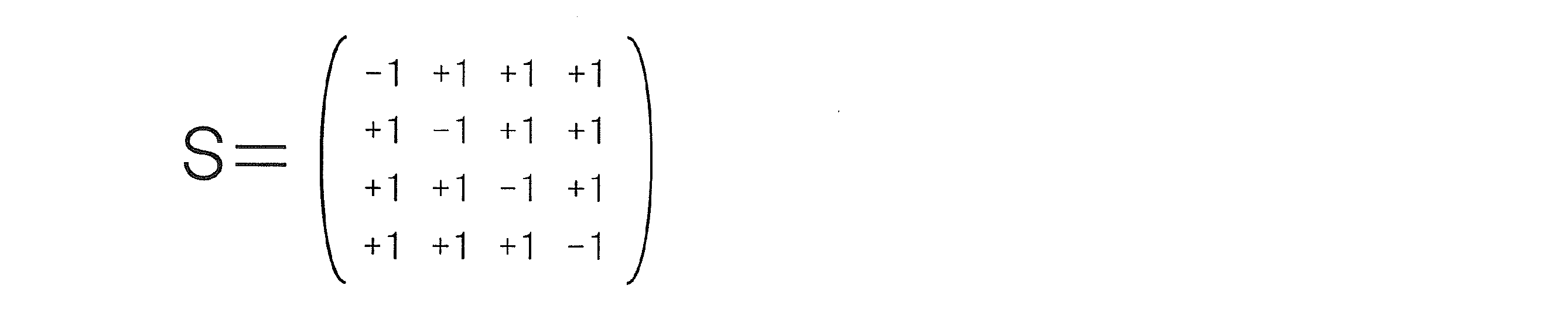
一方で、上記の逆行列S-1は、次のようになる。

これは線型代数学理論における当然の帰結である。
以下、便宜上、前記行列Sをスイッチ行列、前記逆行列S-1を演算行列と呼ぶとともに、最適な手法を導き出すため、以下のように両行列を一般化表示する。
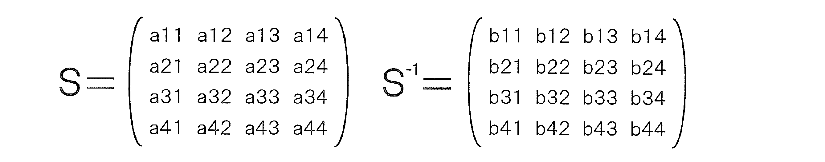
ここで、本発明の実施形態1における前提条件1として、以下の条件を掲げる。
「前提条件1:スイッチ行列Sの各要素は、+1もしくは-1のいずれかである。」
この前提条件は、スイッチの状態を非反転(+1)、もしくは反転(-1)に限定したことによるものである。この限定の理由は以下の通りである。
しかし、前記に限定したとしても、まだ2の16乗通り、すなわち65536通りの行列が考えられる。
「前提条件2:スイッチ行列Sは、逆行列S-1を持たなければならない。」
前提条件2は、線型代数学の理論により、次のように言い換えることもできる。
「前提条件2’:スイッチ行列Sの行列式は、0(ゼロ)であってはならない。」
この前提条件は、本発明が(5)~(8)式によって演算行列(スイッチ行列の逆行列)を求めることができる場合に対してのみ有効であることによるものである。これにより、前記の65536通りが22272通りまで減少する。
V1=b11・P1+b12・P2+b13・P3+b14・P4
・・・(21)
「前提条件3:演算行列の各要素は、+1/4もしくは-1/4のいずれかである。」
ここで、±1/4は、演算行列S-1をスイッチ行列Sの逆行列と定義したために固定化された数値である。実際の運用では、前記でも示した通り、AD変換部4-2の出力の比例係数は任意にとれるのだから、前記よりもう少し緩く条件設定し、
「前提条件3’:演算行列S-1の各要素は、+cもしくは-c(ただしc≠0)のいずれかである。」もしくは、
「前提条件3’’:演算行列S-1の各要素は、すべてゼロでないとともに、各々の絶対値がすべて等しい。」
としても一般性を失わない。
つまり、本発明において最大の効果を発揮するスイッチ行列Sの場合数は384通りある。
しかし、これまでの考察で明らかなように、これら384通りはすべて同じSN比改善効果をもたらすものであり、実際の運用では適宜その384通りの中から選べばよい。
上記の同じ効果をもたらす要因を線型代数学の立場から検証してみる。たとえば、この384通りの中には以下のスイッチ行列S’が含まれている。

操作1:1行目と3行目を各々-1倍する。
操作2:4行目を1行目に、3行目を2行目に、1行目を3行目に、2行目を4行目に入れ替える。
本発明において、操作1は非反転と反転のスイッチ状態をすべて逆さまにしたものであり、これだけの変更ではSN比に影響は与えない。さらに、操作2はセンサの番号付けを変えただけのことであり、何ら一般性を失わない。これと同じ考察をすることによって、この384通りは理論的にはすべて前記のスイッチ行列Sに帰着される。
前記の384通りの中には、先のスイッチ行列S及びS’とは異なる以下のスイッチ行列S’’も含まれている。

操作1:1行目を-1倍する。
操作2:操作1の後に1列目を-1倍する。
これらの2段階の操作によって、前述のスイッチ行列Sに戻る。
(1)「4個のセンサの種類(信号特性)がすべて同じ場合」もしくは「4個のセンサの種類は異なるけれども、同様の信号処理をしたほうがよい場合」
この場合には、スイッチの時間的変化をセンサ4つが互いに対称になるようにするのがよい。したがって、スイッチ行列Sまたはスイッチ行列S’が推奨される。このときの場合の数は、前述の384通りのうち96通り存在する。
この場合には、異なる1個のセンサに対してはスイッチを設けないのがよい。したがって、スイッチ行列S’’が推奨される。このときの場合の数は288通りである。
(1)図3に示す実施形態1の信号処理装置は、センサ1-1~1-4が2端子の電圧出力型の場合であるが、センサ1-1~1-4を2端子の電流出力型に置き換えるようにしても良い。
この場合には、センサ1-1~1-4とこれらに対応するスイッチ2-1~2-5との接続は図3と同様であるが、スイッチ2-1~2-4同士の接続が図3の直列接続から並列接続に変更される。
センサの個数が2個の場合には、これまでと同様の議論によって、スイッチ行列Sとして以下の数6に示す行列、演算行列S-1として以下の数7に示す行列を選べば、SN比が従来よりも√2倍向上することが示される。


この実施形態2は、SN比が小さいセンサの信号のSN比を相対的に大きくすることが可能な信号処理装置に関するものである。
図6は、実施形態2に係る信号処理装置の全体構成を示すブロック図である。
この実施形態2に係る信号処理装置は、図6に示すように、3個の加速度センサ(X軸加速度センサ、Y軸加速度センサ、Z軸加速度センサ)11-1~11-3と、3個の磁気センサ(X軸磁気センサ、Y軸磁気センサ、Z軸磁気センサ)11-4~11-6と、信号増幅部12と、信号反転部13と、結合部14と、測定部15と、演算部16とを備えている。信号反転部13は、センサからの出力を増幅する信号増幅部12と、信号を反転させるための6個のスイッチ13-1~13-6とを備える。
この後の説明によって明らかなように、これらのセンサの個数は6個に限定されるものではなく、2個以上であれば良い。また、センサの種類についても、加速度センサと磁気センサに限定されるものではなく、センサの種類は2種類以上であれば良い。さらに、後述のように、センサの種類は1種類でも良い。
スイッチ13-1~13-6は、センサ11-1~11-6に対応して設けられている。すなわち、スイッチ13-1~13-6のそれぞれは、信号増幅部12を介して、対応するセンサ11-1~11-6に接続され、互いに同様の機能を備えている。
スイッチ13-1は、例えば図7に示すように、2つの入力端子1301、1302と、2つの出力端子1303、1304と、2つの切り換えスイッチ13-1A、13-1Bと、を備えている。
測定部15は、スイッチ13-1~13-6の開閉動作に同期して結合部14で生成される結合信号を順に受け取り、この各結合信号について増幅、AD変換などの所定の処理を行う。
次に、このような構成の実施形態2の動作について説明する。
この実施形態2は、図6に示すように信号増幅部12を含むが、まず図8に示す測定系(構成)について、その動作を説明する。
この測定系は、図8に示すように、図6に示す信号増幅部12を省略し、かつ、X軸加速度センサ11-1とX軸磁気センサ11-4のみの出力信号の処理を対象とする場合である。
スイッチ13-1、13-4の切り換え動作は、制御部(図示せず)からの制御信号により行われるものとする。また、スイッチ13-1、13-4は、図9に示すように第1と第2の動作状態があり、この各動作は第1、第2の期間T1、T2に行う。図9において、スイッチが非反転の出力のときを「+1」で示し、スイッチが反転の出力のときを「-1」で示す。
P1=Sg+Sm・・・(22)
P2=Sg-Sm・・・(23)
Sg’=(P1+P2)/2・・・(24)
Sm’=(P1-P2)/2・・・(25)
図10は、図6において、X軸加速度センサ11-1とX軸磁気センサ11-4のみの出力信号の処理を対象としたブロック図であり、図8との違いは信号増幅部12が追加されている点である。
図10の信号増幅部12では、信号増幅回路12-1を備えている。この信号増幅回路12-1は、例えば図11に示すような減衰器(アッテネータ)などからなる。そして、信号増幅回路12-1の信号レベルの増幅率は、1/α(ただしα≧1)とする。
このため、図10の実施形態2の場合には、測定部15の出力信号P1、P2は式(22)(23)を参照すると、以下のようになる。
P1=(Sg/α)+Sm・・・(22A)
P2=(Sg/α)-Sm・・・(23A)
Sg’=(α/2)×(P1+P2)・・・(24A)
Sm’=(1/2)×(P1-P2)・・・(25A)
次に、図10に示す実施形態2のSN比について、参考例1~3との考察を行う。
(参考例のSN比)
まず、図14に示すような時分割処理によるセンサ信号の測定系を参考例1とし、この参考例1のSN比について検討する。
この参考例1に係る測定系は、図12に示すように、センサ11-1、11-4と、スイッチ18-1、18-2と、測定部15を備えている。そして、スイッチ18-1、18-2のオンにより、時分割でセンサ11-1、11-4の出力信号Sg、Smを測定部15に入力し、これを測定部15から出力信号Sg’、Sm’として出力する。
このようなノイズを含む場合の測定部15の出力信号Sg’、Sm’は、以下のようになる。
Sg’=Sg±Ng±Na・・・(26)
Sm’=Sm±Nm±Na・・・(27)
図8におけるセンサ11-1のセンサノイズを±Ngとし、センサ11-4のセンサノイズを±Nmとする。また、スイッチ13-1、13-4及び結合部14ではノイズの発生はないが、測定部15のノイズを±Naとする。
P1=Sg+Sm±Ng±Nm±Na・・・(28)
P2=Sg-Sm±Ng±Nm±Na・・・(29)
ここで、各ノイズがすべてホワイトノイズである(ノイズスペクトルが周波数に依存しない)とともに互いに独立であると仮定すれば、式(28)(29)は以下のようになる。


センサ感度(加速度センサX軸)>センサ感度(磁気センサX軸)
センサノイズ(加速度センサX軸)=センサノイズ(磁気センサX軸)
このような仮定の下では、両センサのSN比の大小関係は以下のようになる。
センサSN比(加速度センサX軸)>センサSN比(磁気センサX軸)
ここでは、考察を簡単化するために、等しく置いた加速度センサと磁気センサのノイズを±Nsとし、測定部15のノイズ±Naを無視(Na=ゼロと)すると、式(26)(27)から図14の測定部15の出力信号Sg’、Sm’は以下のようになる。
Sg’=Sg±Ng=Sg±Ns・・・(30)
Sm’=Sm±Nm=Sm±Ns・・・(31)
センサSN比(X軸加速度センサ)=Sg/Ns・・・(32)
センサSN比(X軸磁気センサ)=Sm/Ns ・・・(33)
したがって、両センサのSN比の大小関係は、以下のように上記の仮定のままである。
センサSN比(X軸加速度センサ)>センサSN比(X軸磁気センサ)
このため、図12の参考例1では、両センサ11-1、11-4の感度の比Sg:Smが、そのまま信号処理後のセンサ出力のSN比の比となって現れる。
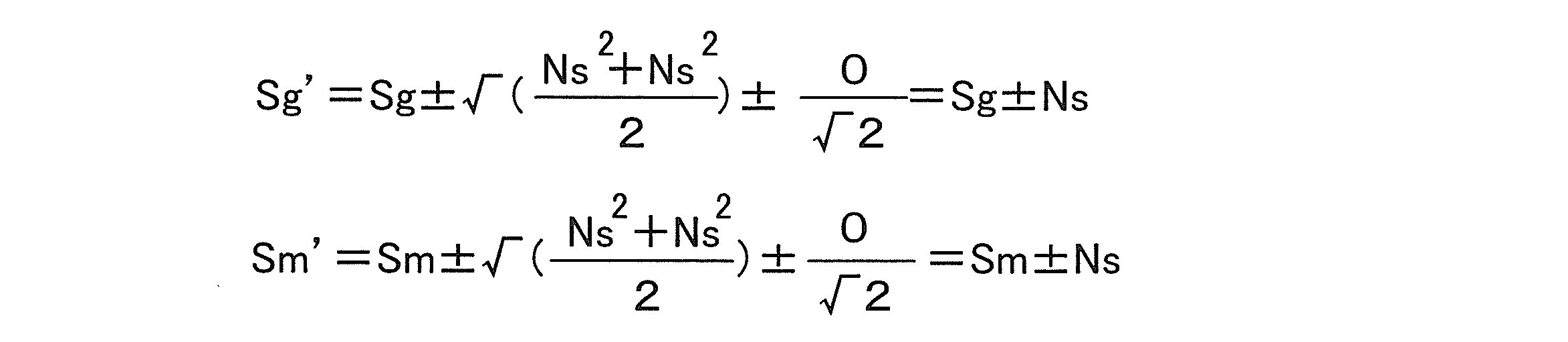
したがって、図8に示す参考例2のセンサ11-1、11-4のSN比に関しても図14に示す参考例1のセンサのSN比と同様の結果が導かれることとなる(式(32)(33)参照)。
図12に示す参考例1及び図8に示す参考例2では、いずれの場合も、2つのセンサ11-1、11-4の感度に大小の差があれば、その大小の差がそのまま信号処理後のSN比に反映されてしまう。したがって、図12に示す参考例1や図8に示す参考例2では、そのSN比の大小関係を逆転させることはできない。
そこで、この実施形態2では、図6または図10に示すように、信号増幅部12を設けることで上記の課題を解決するようにした。
まず、図12に示す参考例1のセンサ11-1、11-4とスイッチ18-1、18-2との間に、図10に示す信号増幅部12を挿入(追加)したものを参考例3とし、この参考例3のSN比について検討する。ここで、信号増幅部12におけるノイズは、一般に非常に小さいので無視する。
この場合には、式(26)(27)を用いると、測定部15の出力信号Sg’、Sm’は、以下のようになる。

Sg’=(Sg±Ns)/α・・・(34)
Sm’=Sm±Ns ・・・(35)
式(34)(35)は、式(30)(31)から求められるSN比と何ら変わらない。したがって、参考例3のように、図12に示す参考例1に図10の信号増幅部12を単に追加してもSN比を逆転させることはできない。
次に、図10に示す実施形態2において、上記の信号処理を行ったときのSN比について検討する。ここで、信号増幅部12でのノイズは、一般に非常に小さいので無視する。
この場合には、ノイズを含む測定部15の出力信号P1、P2は、式(28)(29)及び「数8」に示す2式を参照すると、以下のようになる。


すなわち、X軸加速度センサ11-1のノイズの変化は、以下のようになる。


すなわち、X軸加速度センサ11-1のSN比の変化(=SNgとすると)は、以下のようになる。


SNg≦1 ・・・(36)
SNm≧1 ・・・(37)
したがって、この実施形態2によれば、参考例1~3と比べて、X軸加速度センサ11-1のSN比は悪化するが、X軸磁気センサ11-4のSN比は向上する。
以上のように、この実施形態2によれば、図6または図10に示すように信号増幅部12を設けるとともに、上記のような信号処理を実施するようにしたので、センサのSN比の大小関係とは逆のSN比の大小関係を作り出すことが可能となる。
しかも、この実施形態2では、信号増幅回路12-1の増幅率は任意に設定することが可能であるので、たとえば1/β倍(ただしα<β)とすれば、センサ自身のSN比の大小関係を信号処理後に逆転させることが可能となる。
加速度センサのSN比(1Gに対するセンサ出力を加速度センサノイズで割ったもの)が、磁気センサのSN比(50uTに対するセンサ出力を磁気センサノイズで割ったもの)のγ倍(γ≧1)であるものとする。
また、図10の例では、信号処理後のSN比が低くなっても良い側のセンサに対して増幅率を1/α倍(α≧1)と設定する場合について説明した。しかし、逆に信号処理後のSN比を高くしたい側のセンサに対してα倍(α≧1)の増幅をする場合には、信号増幅部12の構成要素として信号増幅回路が採用され、理論上は全く同様の効果が得られる。
本実施形態2を具体化する場合を考えると、センサ信号が極端に小さい場合を除けば、増幅率が1.0より大きい信号増幅回路よりも増幅率が1.0より小さい信号増幅回路(減衰回路)を使うほうがより良いものと考えられる。その理由は、減衰回路は信号増幅回路と比較して回路規模が小さい、増幅動作をさせるための電力が少ない、ノイズが小さい、などの利点を持っているためである。
例えば、同種のセンサA-1とセンサA-2とがあり、感度、ノイズ、及びSN比がいずれも同じであるが、信号処理後のSN比はセンサA-1のほうを高くしたいときには、信号増幅部12でセンサA-1の出力信号を1.0倍より大きい増幅率で増幅しても良いし、センサA-2の出力信号を1.0倍より小さい増幅率で増幅させても良い。
図13は、センサ1-1、1-4のノイズ±Ng、±Nmが、±Ng≠±Nmというように異なる場合である。
実際には、まず任意の正の数α2を定義し、|±Ng|/α2=|±Nm|となるように操作する。この操作は特別なものではなく、これまでに説明した信号増幅部12によって、もとのX軸加速度センサの出力を増幅または減衰させれば良い。この操作を行えば、その後の信号処理方法は全く同じであるし、それ故その後の計算も全く同じようにして導かれる。
センサの最終のSN比の計算結果は、図13に示した通りであるが、補足すれば以下のようになる。
磁気センサのSN比の式は、従前のαがα1となっただけで、他は何も変わっていない。
また、加速度センサのSN比は、α2の大きさ、すなわちもとのセンサノイズの大きさによって大きくなったり小さくなったりする。しかし、もとの加速度センサのSN比がもとの磁気センサのSN比よりも大きいことを条件とすれば、α2<α1という大小関係が前提となる。したがって、SN比が無限に小さくなるようなことはない。
次に、この実施形態2の変形例について、図14を参照して説明する。
図10に示す実施形態2に係る信号処理装置では、加速度センサ11-1と磁気センサ11-4の2種類(2個)を対象としたが、この変形例は、図14に示すように、4種類のセンサ11-7~11-10に置き換えたものである。
4種類のセンサ11-7~11-10は、以下の関係にあるものとする。
センサ11-7・・・もともとの感度が高く、SN比も大きい。
センサ11-8・・・感度及びSN比とも2番目に大きい。
センサ11-9・・・感度及びSN比とも3番目に大きい。
センサ11-10・・・もともとの感度が上記3つより低く、センサ近傍での増幅回路が必要。
すなわち、センサ11-7の出力をもっとも大きく減衰させるために、センサ11-7とスイッチ13-7との間に、減衰率が最も大きな信号増幅回路12-2を挿入した。
センサ11-8の出力を減衰させるために、センサ11-8とスイッチ13-8との間に、信号増幅回路12-2の減衰率よりも減衰率が小さな信号増幅回路12-3を挿入した。いま、信号増幅回路12-2の減衰率を1/α2、信号増幅回路12-3の減衰率を1/α3としたとき、1>1/α3>1/α2となるように減衰率を設定する。
センサ11-9の出力は、減衰や増幅をすることなく、そのままスイッチ13-9に供給するようにした。
この変形例からも明らかなように、この信号増幅部12における増幅や減衰の機能は、あくまでセンサ相互の相対的なSN比を変化させるためにある。したがって、対象となるすべてのセンサを減衰、または対象となるすべてのセンサを増幅するような構成は無駄な構成である。このため、少なくとも1つのセンサは、センサ信号をそのまま(増幅も減衰もしない)次段のスイッチに伝達することが合理的な構成となる。図14では、そのセンサ信号として、センサ11-9を選んでいる。
(実施形態3の構成)
図15は、本発明に係る信号処理装置の実施形態3の構成例を示すブロック図である。
この実施形態3に係る信号処理装置は、図15に示すように、n個のセンサ21-1~21-nと、n個の増幅・スイッチ22-1~22-nを備える信号反転部22と、結合部23と、測定部24と、演算部25とを備えている。信号反転部22は信号反転機能と共に増幅機能を併せ持っている。
n個の増幅・スイッチ22-1~22-nは、n個のセンサ21-1~21-nに対応して設けられている。すなわち、増幅・スイッチ22-1~22-nのそれぞれは、対応するセンサ21-1~1-nに接続され、同様の機能を備えている。信号反転部22の具体例は後述する。
ここで、センサ21-1~21-nは2端子型センサとする場合には、例えば電圧出力型と電流出力型がある。このため、センサ21-1~21-nが電圧出力型の場合には各出力信号は直列に結合されて結合信号が生成され、電流出力型の場合には各出力信号は並列に結合されて結合信号が生成される。
測定部24は、信号反転部22の動作に同期して結合部23で生成される結合信号C1~Cnを順に受け取り、この各結合信号C1~Cnについて増幅、AD変換などの所定の処理を行う。
演算部25によるセンサ21-1~21-nの各出力値の演算処理は、CPU(中央処理装置)またはコンピュータによるソフトウェアなどによって実現できる。
図16は、図15に示す実施形態3において、センサ21-1~21-nとして2端子の電圧出力型のセンサを採用する場合の構成例を示す。
この実施形態3に係る信号処理装置は、図16に示すように、n個のセンサ21-1~21-nと、信号反転部22Aと、測定部24と、演算部25とを備えている。
そして、この実施形態3は、図15に示す実施形態3の信号反転部22及び結合部23に相当する構成を、図16の信号反転部22Aにより具体化したものである。
信号反転部22Aは、図16に示すように、増幅・スイッチ22-1~22-nを備えている。
スイッチ群22-1aはスイッチ22-1A~22-1Fを備え、スイッチ群22-2aはスイッチ22-2A~22-2Fを備えている。同様に、スイッチ群22-naは、スイッチ22-nA~2-nFを備えている。
ここで、図16の例では、n個の増幅・スイッチ22-1~22-nのそれぞれは、同一の増幅器22-Aを使用(共有)するようになっているが、増幅器を個別に設けるようにしても良い。
演算部25は、測定部24から出力される出力データの電圧P1~Pnを所定の演算により線型結合させ、この線型結合を基に、センサ21-1~21-nの各出力値を求める所定の演算を行い、この演算結果を出力する。
次に、実施形態3の動作例について、図面を参照して説明する。
図16において、増幅・スイッチ22-1~22-nのスイッチ群22-1a、22-2a・・・22-naのスイッチの切り換え動作は、制御部(図示せず)からの制御信号により行われるものとする。
増幅・スイッチ22-1~22-nのスイッチ群22-1a~22-naは、図17に示すように1サイクル中に第1~第nの動作状態があり、この各動作は第1~第nの期間T1~Tnに行う。
このような第1~第nの期間T1~Tnにおける増幅・スイッチ22-1~22-nの切り換え動作をまとめると、図17に示すようになる。
また、増幅・スイッチ22-2により得られる電圧は、期間T2にセンサ21-2の出力電圧V2を-α倍した電圧-αV2が得られ、それ以外の各期間T1、T3~Tnにはその出力電圧V2を+1倍した非反転の電圧V2が得られる。
図17では、増幅・スイッチ22-1~22-nにより得られる各電圧が、非反転の電圧のときは「+1」で示し、-α倍された電圧のときは「-α」で示す。
P1=-αV1+V2+V3+・・・+Vn・・・(38-1)
P2=V1-αV2+V3+・・・+Vn ・・・(38-2)
P3=V1+V2-αV3+・・・+Vn ・・・(38-3)
・・・
Pn=V1+V2+V3+・・・-αVn ・・・(38-n)
V1=1/β・[(α-n+2)P1+P2+P3+・・・+Pn]
・・・(39-1)
V2=1/β・[P1+(α-n+2)P2+P3+・・・+Pn]
・・・(39-2)
V3=1/β・[P1+P2+(α-n+2)P3+・・・+Pn]
・・・(39-3)
・・・・
Vn=1/β・[P1+P2+P3+・・・+(α-n+2)Pn]
・・・(39-n)
ただし、β=-α2+(n-2)α+n-1である。
たとえば、n=6とすれば、信号反転部2Aの出力電圧P1~P6は以下のようになる。
P1=-αV1+V2+V3+V4+V5+V6・・・(40-1)
P2=V1-αV2+V3+V4+V5+V6 ・・・(40-2)
P3=V1+V2-αV3+V4+V5+V6 ・・・(40-3)
P4=V1+V2+V3-αV4+V5+V6 ・・・(40-4)
P5=V1+V2+V3+V4-αV5+V6 ・・・(40-5)
P6=V1+V2+V3+V4+V5-αV6 ・・・(40-6)
V1=1/β・[(α-4)P1+P2+P3+P4+P5+P6]
・・・(41-1)
V2=1/β・[P1+(α-4)P2+P3+P4+P5+P6]
・・・(41-2)
V3=1/β・[P1+P2+(α-4)P3+P4+P5+P6]
・・・(41-3)
V4=1/β・[P1+P2+P3+(α-4)P4+P5+P6]
・・・(41-4)
V5=1/β・[P1+P2+P3+P4+(α-4)P5+P6]
・・・(41-5)
V6=1/β・[P1+P2+P3+P4+P5+(α-4)P6]
・・・(41-6)
ただし、β=-α2+4α+5である。
図18は、図16の測定系と図17の動作タイミングにおいて、ノイズ(雑音)を重畳させた場合を示したものである。ただし、図示の実施形態3は、図15を基本にしている。
また、信号反転部22及び結合部23では、新たにノイズが発生することはないが、センサノイズと増幅率に応じたノイズがそのまま出力されるものとする。一方、測定部24では増幅部やAD変換部などで測定ノイズが新たに発生するものとし、この測定ノイズを±Naとして定める。
したがって、ノイズを含む出力電圧P1~Pnは、上記の(38-1)~(38-n)式を参照することにより以下のようになる。
P1=-α(V1±Ns)+(V2±Ns)
+(V3±Ns)+・・・+(Vn±Ns)±Na
・・・(42-1)
P2=(V1±Ns)-α(V2±Ns)
+(V3±Ns)+・・・+(Vn±Ns)±Na
・・・(42-2)
P3=(V1±Ns)+(V2±Ns)
-α(V3±Ns)+・・・+(Vn±Ns)±Na
・・・(42-3)
・・・
Pn=(V1±Ns)+(V2±Ns)
+(V3±Ns)+・・・-α(Vn±Ns)±Na
・・・(42-n)
P1=-αV1+V2+V3+・・・+Vn±√(α2+n-1)Ns±Na
・・・(43-1)
P2=V1-αV2+V3+・・・+Vn±√(α2+n-1)Ns±Na
・・・(43-2)
P3=V1+V2-αV3+・・・+Vn±√(α2+n-1)Ns±Na
・・・(43-3)
・・・
Pn=V1+V2+V3+・・・-αVn±√(α2+n-1)Ns±Na
・・・(43-n)
このn個の式に対し、上記の(39-1)~(39-n)式のV1~Vnと同じ演算を行う。仮にセンサ21-1の出力V1を求めたければ、1/β・[(α-n+2)P1+P2+P3+・・・+Pn)を計算すれば良い。
したがって、センサノイズ及び測定ノイズを考慮したときの各センサの出力V1’~Vn’は、以下のようになる。
V1’=V1±γ/β(ηNs±Na)・・・(44-1)
V2’=V2±γ/β(ηNs±Na)・・・(44-2)
V3’=V3±γ/β(ηNs±Na)・・・(44-3)
・・・
Vn’=Vn±γ/β(ηNs±Na)・・・(44-n)
β=-α2+(n-2)α+n-1・・・(45-1)
γ=√[α2+(-2n+4)α+n2-3n+3]・・・(45-2)
η=√(α2+n-1)・・・(45-3)
基本的には、n個のセンサに対して上記の式(44-1)~(45-3)を用いて、増幅器22-Aの増幅率αを決めれば良い。以下、具体例を2つ挙げてSN比を考察する。
この具体例1は、センサが6個のときに測定ノイズを最小にする場合である。
すなわち、n=6のときである。これまでの計算を適用すると、以下のようになる。
V1’=V1±γ/β(ηNs±Na)・・・(46-1)
V2’=V2±γ/β(ηNs±Na)・・・(46-2)
V3’=V3±γ/β(ηNs±Na)・・・(46-3)
V4’=V4±γ/β(ηNs±Na)・・・(46-4)
V5’=V5±γ/β(ηNs±Na)・・・(46-5)
V6’=V6±γ/β(ηNs±Na)・・・(46-6)
β=-α2+4α+5・・・(47-1)
γ=√(α2-8α+21)・・・(47-2)
η=√(α2+5)・・・(47-3)
微分計算もしくは数値計算等の結果、f6はα≒1.21において最小値0.30を取ることが示される。このとき、β≒8.38、γ≒3.58、η≒2.54である。
V1’≒V1±1.09Ns±0.30Na・・・(48-1)
V2’≒V2±1.09Ns±0.30Na・・・(48-2)
V3’≒V3±1.09Ns±0.30Na・・・(48-3)
V4’≒V4±1.09Ns±0.30Na・・・(48-4)
V5’≒V5±1.09Ns±0.30Na・・・(48-5)
V6’≒V6±1.09Ns±0.30Na・・・(48-6)
この(48-1)~(48-6)式を見ると、センサノイズ±Nsが無視できるほど小さい場合には、従来の時分割処理と比べてSN比で1/0.30倍、つまり約3.3倍向上することがわかる。
この具体例2は、センサがn個のときにセンサノイズを最小にする場合である。
上記の式(45-1)~(45-3)において、fn=γη/βを最小にするαを計算すると、α=n/2-1となり、さらに、最小値はnにかかわらず常にfn=1であることが示される。
V1’=V1±Ns±(2/n)Na・・・(49-1)
V2’=V2±Ns±(2/n)Na・・・(49-2)
・・・
Vn’=Vn±Ns±(2/n)Na・・・(49-n)
これまでの考察結果を踏まえると、センサの個数が何個であれ、本発明に係る実施形態3(測定系)を備えつつ、これまでと同様の計算を実行し、増幅器22-Aの増幅率αを求めれば最適な(もっともSN比の良い)信号処理装置を構成することが可能となる。
なお、当然のことながら、センサノイズと測定ノイズを合算したノイズを最小にする場合においても、これまでの計算と同様の手順で設定可能であることは言うまでもない。
この実施形態4は、センサに抵抗型センサを使用する場合に好適な信号処理装置である。
(実施形態4の構成)
図19は、本発明の信号処理装置の実施形態4の構成例を示すブロック図である。
この実施形態4は、図19に示すように、4個の抵抗型センサ31-1~31-4と、検出回路形成部32と、測定部33と、演算部34とを備えている。
4個の抵抗型センサ31-1~31-4のそれぞれは、何らかの物理量の変化が電気抵抗値の変化によって検知可能なものであり、この定義は抵抗型センサの一般的な慣例に従うものである。
なお、r及びRについては抵抗値そのものであるので必ず正の値(ゼロより大きい)を取るが、ΔRについては正でも負でもゼロでもよい。
r1=R1+ΔR1・・・(50)
r2=R2+ΔR2・・・(51)
r3=R3+ΔR3・・・(52)
r4=R4+ΔR4・・・(53)
なお、4個の抵抗型センサ31-1~31-4のそれぞれは、図19に示すように出力端子を備えるようにしても良い。
検出回路形成部32は、物理量の測定のときに、4個の抵抗型センサ31-1~31-4のうちから予め定めた2個の抵抗型センサを選択し、図20A~図20Dに示すように、この選択した2個の抵抗型センサを含む予め定めた抵抗検出回路321~324を順に形成または組み立てるものである。
検出回路形成部32では、物理量の測定の1サイクルの期間内にフェーズ1~4の各動作を順に行い、そのフェーズ1~4に応じて図20A~図20Dに示すような4個の抵抗検出回路321~324が形成される。
フェーズ2では、図20Bに示すように、抵抗型センサ31-2、31-3に係る抵抗r2、r3と参照用の2つの抵抗Rrefとを組み込んだ、フルブリッジ回路からなる抵抗検出回路322が形成される。
フェーズ4では、図20Dに示すように、抵抗型センサ31-1、31-4に係る抵抗r1、r4と参照用の2つの抵抗Rrefを組み込んだ、フルブリッジ回路からなる抵抗検出回路324が形成される。
フェーズ1における抵抗検出回路321の出力電圧V1は、電源供給端子325に供給される電圧をVとすると、以下のようになる(図20A参照)。


V1=A1-B1・(ΔR1+ΔR3)・・・(54)
V1∝ΔR1+ΔR3・・・(55)
V1=ΔR1+ΔR3・・・(56)
次に、フェーズ2における抵抗検出回路322の出力電圧V2を求めると、以下のようになる(図20B参照)。

V2=A2-B2・(ΔR3-ΔR2)・・・(57)
V2=ΔR3-ΔR2・・・(58)
このため、検出回路形成部32において、フェーズごとに出力される出力電圧V1~V4をまとめると、以下のようになる。
V1=ΔR1+ΔR3 ・・・(59)
V2=ΔR3-ΔR2 ・・・(60)
V3=ΔR2+ΔR4 ・・・(61)
V4=-ΔR4+ΔR1・・・(62)
本実施形態4の場合、抵抗値相互の減算結果を電圧値に変換する場合があるため、コストや精度の観点から、特にフルブリッジ回路が最適である。
また、検出回路形成部32の後段に、トランジスタや増幅器が存在しても良い。
このため、測定部33は、例えば、抵抗検出回路321~324から出力される出力電圧V1~V4を増幅する演算増幅器(オペアンプ)からなる増幅回路(図示せず)と、増幅回路の出力をAD変換するAD変換回路(図示せず)と、を備えている。
ここで、測定部33は、上記のように、検出回路形成部32から取り込んだ出力電圧V1~V4についてAD変換回路でAD変換してデジタル信号として出力する。このため、演算部34による各軸の出力の演算は、CPU(中央処理装置)またはコンピュータによるソフトウェアなどによって実現できる。
次に、本発明の実施形態4の具体例について説明する。
まず、具体例1について説明する。
この具体例1は、図19に示す実施形態4において、抵抗型センサ31-1~31-4として、以下のような出力特性を有する磁気抵抗型のセンサを適用した場合である。
ΔR1=X+Z=kx・Bx+kz・Bz・・・(63)
ΔR2=X-Z=kx・Bx-kz・Bz・・・(64)
ΔR3=Y+Z=ky・By+kz・Bz・・・(65)
ΔR4=Y-Z=ky・By-kz・Bz・・・(66)
なお、式(63)~(66)で示すような出力特性を有する磁気抵抗型のセンサの具体的な内部構成は、特開2002-71381号公報などに記載のように公知である。
フェーズ1:V1(時分割)=ΔR1=X+Z・・・(67)
フェーズ2:V2(時分割)=ΔR2=X-Z・・・(68)
フェーズ3:V3(時分割)=ΔR3=Y+Z・・・(69)
フェーズ4:V4(時分割)=ΔR4=Y-Z・・・(70)
X軸磁場:X=1/2・(V1(時分割)+V2(時分割))
・・・(71)
Y軸磁場:Y=1/2・(V3(時分割)+V4(時分割))
・・・(72)
Z軸磁場:Z=1/4・(V1(時分割)-V2(時分割)
+V3(時分割)-V4(時分割))
・・・(73)
フェーズ1:V1=ΔR1+ΔR3=X+Y+2Z ・・・(74)
フェーズ2:V2=ΔR3-ΔR2=-X+Y+2Z・・・(75)
フェーズ3:V3=ΔR2+ΔR4=X+Y-2Z ・・・(76)
フェーズ4:V4=-ΔR4+ΔR1=X-Y+2Z・・・(77)
この演算は、具体的には以下のようになる。
X軸磁場:X=1/4・(V1-V2+V3+V4)・・・(78)
Y軸磁場:Y=1/4・(V1+V2+V3-V4)・・・(79)
Z軸磁場:Z=1/8・(V1+V2-V3+V4)・・・(80)
なお、上記までの説明で明らかなように、Bx、By、Bz乃至X、Y、Zは、特に3軸磁場の成分値でなくても良く、4個の抵抗型センサに対して式(63)~(66)を満たすようなセンサであれば元の物理量は磁場に限るものではない。
さて、上記の式(74)~(77)は、WO2008/032741号公報に記載の〔数9〕と酷似している。そのまま〔数9〕を抜粋すると、以下のようになる。
(α)=A+C=Hx+Hy+2Hz+√2n ・・・(81)
(β)=A+D=Hx-Hy+2Hz+√2n ・・・(82)
(γ)=B+D=-Hx-Hy+2Hz+√2n・・・(83)
(δ)=B+C=-Hx+Hy+2Hz+√2n・・・(84)
このうち、式(74)と式(81)は、(α)と(ノイズnを除いて)まったく同じ式である。式(75)と式(76)は式(82)と式(84)を逆にしたものと同様であるが、式(75)と式(76)の入れ替えは上記のとおり設計事項であるので、本質的な意味はいずれも同じである。
(γ)=-B-D・・・(85)
そのため、まず実施形態4の具体例1の比較対象である時分割処理の場合の各フェーズでの信号成分、ノイズ成分を以下のように定義する。
フェーズ1:V1(時分割)=ΔR1=X+Z±Ns±Na・・・(86)
フェーズ2:V2(時分割)=ΔR2=X-Z±Ns±Na・・・(87)
フェーズ3:V3(時分割)=ΔR3=Y+Z±Ns±Na・・・(88)
フェーズ4:V4(時分割)=ΔR4=Y-Z±Ns±Na・・・(89)
X軸磁場(ノイズ含む):X’=1/2・(2X±√2Ns±√2Na)
・・・(90)
Y軸磁場(ノイズ含む):Y’=1/2・(2Y±√2Ns±√2Na)
・・・(91)
Z軸磁場(ノイズ含む):Z’=1/4・(4Z±2Ns±2Na)
・・・(92)
フェーズ1:V1=ΔR1+ΔR3
=(X+Z±Ns)+(Y+Z±Ns)±Na
=X+Y+2Z±√2Ns±Na ・・・(93)
フェーズ2:V2=ΔR3-ΔR2
=(Y+Z±Ns)-(X-Z±Ns)±Na
=-X+Y+2Z±√2Ns±Na ・・・(94)
フェーズ3:V3=ΔR2+ΔR4
=(X-Z±Ns)+(Y-Z±Ns)±Na
=X+Y-2Z±√2Ns±Na ・・・(95)
フェーズ4:V4=-ΔR4+ΔR1
=-(Y-Z±Ns)+(X+Z±Ns)±Na
=X-Y+2Z±√2Ns±Na ・・・(96)
X軸磁場(ノイズ含む):X’=1/4・(4X±2√2Ns±2Na)
・・・(97)
Y軸磁場(ノイズ含む):Y’=1/4・(4Y±2√2Ns±2Na)
・・・(98)
Z軸磁場(ノイズ含む):Z’=1/8・(8Z±2√2Ns±2Na)
・・・(99)
X軸SN比:Nsに対するSN比は同じ。Naに対するSN比は√2倍向上。
Y軸SN比:Nsに対するSN比は同じ。Naに対するSN比は√2倍向上。
Z軸SN比:Nsに対するSN比は√2倍向上。Naに対するSN比は2倍向上。
X軸SN比:Naに対するSN比は√6/2倍(約1.22倍)向上。
Y軸SN比:Naに対するSN比は√6/2倍(約1.22倍)向上。
Z軸SN比:Naに対するSN比は√3倍(約1.73倍)向上。
したがって、抵抗型センサに起因するノイズが非常に小さく、測定部33に起因するノイズと比べて無視できるとしたときに、実施形態4の具体例1は最大の効果を発揮する。
次に、実施形態4の具体例2について説明する。
この具体例2は、図19に示す実施形態4において、抵抗型センサ31-1~31-4として、以下のような出力特性を有する磁気抵抗型のセンサを適用したものである。
ΔR1=X+Z+Yx=kx・Bx+kz・Bz+kyx・By
・・・(100)
ΔR2=X-Z+Yx=kx・Bx-kz・Bz+kyx・By
・・・(101)
ΔR3=Y+Z+Xy=ky・By+kz・Bz+kxy・Bx
・・・(102)
ΔR4=Y-Z+Xy=ky・By-kz・Bz+kxy・Bx
・・・(103)
なお、式(100)~(103)で示すような出力特性を有する磁気抵抗型のセンサの具体的な内部構成は、特開2002-71381号公報などに記載のように公知である。
フェーズ1:V1=ΔR1+ΔR3=(X+Yx)+(Y+Xy)+2Z
・・・(104)
フェーズ2:V2=ΔR3-ΔR2=-(X+Yx)+(Y+Xy)+2Z
・・・(105)
フェーズ3:V3=ΔR2+ΔR4=(X+Yx)+(Y+Xy)-2Z
・・・(106)
フェーズ4:V4=-ΔR4+ΔR1=(X+Yx)-(Y+Xy)+2Z
・・・(107)
これを具体的に書けば、以下のようになる。
X+Yx=1/4・(V1-V2+V3+V4) ・・・(108)
Y+Xy=1/4・(V1+V2+V3-V4) ・・・(109)
Z=1/8・(V1+V2-V3+V4) ・・・(110)
この式(108)~(110)の結果を見ると、式(110)によりZ軸の磁場はすでに求められている。実際には、実施形態4の具体例1とまったく同じ式である。つまり、SN比の向上については具体例1とまったく同じ結論が成立する。
V1-V2+V3+V4=4(X+Yx)
=4(kx・Bx+kyx・By)=P1
・・・(111)
V1+V2+V3-V4=4(Y+Xy)
=4(kxy・Bx+ky・By)=P2
・・・(112)
式(111)(112)で定義したP1及びP2を用いて具体的に書けば、以下のようになる。

以上説明したように、本発明の実施形態4によれば、検出回路形成部32が、物理量の測定のときに、4個の抵抗型センサ31-1~31-4のうちの予め定めた2個の抵抗型センサを選択し、この選択した2個の抵抗型センサを含む予め定めた抵抗検出回路321~324を形成するようにした。
このため、この実施形態4によれば、複数の抵抗検出回路を必要とする場合に、構成要素の共通化を図って回路規模などの小型化を図ることができる上に、SN比の改善に寄与することができる。
2、2A…信号反転部
2-1~2-4…スイッチ
3…結合部
4…測定部
4-1…増幅部
4-2…AD変換部
5…演算部
11-1~11-3…加速度センサ
11-4~11-6…磁気センサ
11-7~11-10…センサ
12…信号増幅部
12-1~12-4…信号増幅回路
13-1~13-10…スイッチ
14…結合部
15…測定部
16…演算部
21-1~21-n…センサ
22、22A…信号反転部
22-1~22-n…増幅・スイッチ
22-1a~22-na…スイッチ群
22-A…増幅器
23…結合部
24…測定部
25…演算部
31-1~31-4…抵抗型センサ
32…検出回路形成部
33…測定部
34…演算部
321~324…抵抗検出回路
Claims (22)
- 所望の物理量に基づく信号成分を含んだ複数の物理量信号それぞれに基づく複数の要素信号を、前記物理量信号の数以上の回数だけ結合して互いに相異なる結合信号を出力する結合部と、
前記結合部から出力される結合信号を順に受け取る測定部と、
前記測定部から順に出力される前記結合信号に基づいて生成された信号から前記所望の物理量に基づく信号成分を求める演算部と、
を備えることを特徴とする信号処理装置。 - 前記演算部は、
前記測定部から順に出力される前記結合信号を線型結合させ、該線型結合させた結果から前記所望の物理量に基づく信号成分を求めることを特徴とする請求項1に記載の信号処理装置。 - 前記演算部における線型結合演算する変換と、前記結合部における結合信号を規定する変換と、が互いに逆の線型変換であることを特徴とする請求項2に記載の信号処理装置。
- 前記物理量信号の数が4つ以上であることを特徴とする請求項1から請求項3のいずれか1項に記載の信号処理装置。
- 前記結合部における結合信号の出力回数が前記物理量信号の数と同じであるとともに、さらに前記逆の線型変換が互いに逆行列の関係であることを特徴とする請求項3に記載の信号処理装置。
- 前記複数の物理量信号を受け取り、当該物理量信号それぞれに対応する前記要素信号のうち、予め定めた信号については、前記物理量信号を反転した反転信号を前記要素信号とし、残りの信号については前記物理量信号を反転せずに非反転信号を前記要素信号として出力する信号反転部と、をさらに備え、
前記結合部は、
前記反転信号と前記非反転信号とを前記物理量信号の数以上の回数だけ結合して、前記結合信号を出力することを特徴とする請求項1から5の何れか1項に記載の信号処理装置。 - 前記信号反転部は、
前記複数の物理量信号を受け取り、当該物理量信号のうち1以上の信号については、前記物理量信号を所定の増幅率で増幅し、残りの信号については前記物理量信号を、そのまま、又は、前記所定の増幅率とは異なる増幅率で増幅する増幅処理を行い、
且つ、
前記複数の物理量信号のうち、予め定めた信号については、前記物理量信号を反転して反転信号とし、残りの信号については前記物理量信号を反転せずに非反転信号とする反転処理を行い、
前記物理量信号それぞれに対して前記増幅処理及び前記反転処理を行った信号を前記要素信号として出力し、
前記結合部は、
前記要素信号のうち、前記反転信号からなる要素信号と前記非反転信号からなる要素信号とを前記物理量信号の数以上の回数だけ結合して、前記結合信号を出力することを特徴とする請求項6に記載の信号処理装置。 - 前記信号反転部は、
前記物理量信号それぞれに対応する要素信号のうち、最もSN比が小さい信号を絶対値で1.0よりも大きい所定の増幅率で増幅し、残りの信号を、そのまま、又は、前記所定の増幅率よりも絶対値が小さい増幅率で増幅することを特徴とする請求項7に記載の信号処理装置。 - 前記信号反転部は、
前記物理量信号それぞれに対応する要素信号のうち、最もSN比が小さい信号をそのまま出力し、残りの信号を絶対値で1.0よりも小さい所定の増幅率で増幅することを特徴とする請求項7に記載の信号処理装置。 - 前記物理量信号の数がN個(ただし、Nは5以上の整数)以上であり、
前記信号反転部は、前記予め定めた信号を((N/2)-1)倍に反転増幅して反転信号とすることを特徴とする請求項7から請求項9の何れか1項に記載の信号処理装置。 - 前記演算部は、
前記結合部から出力される結合信号と、所定の係数とを線型結合した線型結合データに基づき前記所望の物理量に基づく信号成分を求めるようになっており、前記係数は、0を含まず、且つ、絶対値が全て等しいことを特徴とする請求項1から請求項10の何れか1項に記載の信号処理装置。 - 前記物理量信号が、異なる物理量を計測する少なくとも2種類のセンサから出力される信号であることを特徴とする請求項1から請求項11の何れか1項に記載の信号処理装置。
- 前記物理量信号が、2つ以上のセンサから出力される信号であり、前記2つ以上のセンサには、感度及びSN比のうちの少なくとも一方が他のセンサと異なるセンサが含まれることを特徴とする請求項1から請求項12の何れか1項に記載の信号処理装置。
- 特定の物理量を検知し、当該検知量に応じて抵抗が変化する複数の抵抗型センサと、
前記複数の抵抗型センサのうち予め定めた2個以上の抵抗型センサを選択し、当該選択した2個以上の抵抗型センサを含む予め定めた抵抗検出回路を形成する検出回路形成部と、
当該形成された抵抗検出回路の出力信号を順に受け取る測定部と、
前記測定部から順に出力される出力信号について線型結合を含む演算によって前記物理量を求める演算部と、
を備えることを特徴とする信号処理装置。 - 前記検出回路形成部は、前記複数の抵抗型センサの中から時間ごとに異なる2個以上の抵抗型を選択し、当該選択した2個以上の抵抗型センサを含む予め定めた抵抗検出回路を形成することを特徴とする請求項14に記載の信号処理装置。
- 前記複数の抵抗型センサは3つ以上の抵抗型センサであることを特徴とする請求項14又は請求項15に記載の信号処理装置。
- 前記検出回路形成部は、前記複数の抵抗型センサのうち、予め定めた互いに独立な物理量を検知する2個以上の抵抗型センサを選択し、当該選択した2個以上の抵抗型センサを含む予め定めた抵抗検出回路を形成することを特徴とする請求項14から請求項16の何れか1項に記載の信号処理装置。
- 前記選択された2個以上の抵抗型センサは、直交する2軸以上の物理量または2種以上の物理量を同時に検知し、当該検知量に応じた抵抗変化をするセンサであることを特徴とする請求項14から請求項17の何れか1項に記載の信号処理装置。
- 前記演算部は、前記特定の物理量の直交する2軸または3軸方向の成分を演算することを特徴とする請求項14から請求項18の何れか1項に記載の信号処理装置。
- 前記特定の物理量は、磁場であることを特徴とする請求項14から請求項19の何れか1項に記載の信号処理装置。
- 前記抵抗検出回路は、ハーフブリッジ回路及びフルブリッジ回路のうちのいずれかで構成され、
前記検出回路形成部は、前記ハーフブリッジ回路とフルブリッジ回路とを交互に形成することを特徴とする請求項14から請求項20の何れか1項に記載の信号処理装置。 - 前記演算部は、
前記測定部で順に受け取った前記抵抗検出回路からの出力信号と、該抵抗検出回路からの出力信号に対応する係数と、を線型結合させて線型結合データを生成することを特徴とする請求項14から請求項21の何れか1項に記載の信号処理装置。
Priority Applications (7)
| Application Number | Priority Date | Filing Date | Title |
|---|---|---|---|
| EP13743182.1A EP2796835B1 (en) | 2012-02-03 | 2013-01-25 | Signal processing device |
| KR1020147012665A KR101564181B1 (ko) | 2012-02-03 | 2013-01-25 | 신호 처리 장치 |
| US14/374,339 US9148158B2 (en) | 2012-02-03 | 2013-01-25 | Signal processing device |
| EP16150173.9A EP3026397B1 (en) | 2012-02-03 | 2013-01-25 | Signal processing device |
| JP2013556253A JP5777737B2 (ja) | 2012-02-03 | 2013-01-25 | 信号処理装置 |
| CN201380006791.2A CN104081164B (zh) | 2012-02-03 | 2013-01-25 | 信号处理装置 |
| US14/708,802 US9654129B2 (en) | 2012-02-03 | 2015-05-11 | Signal processing device |
Applications Claiming Priority (8)
| Application Number | Priority Date | Filing Date | Title |
|---|---|---|---|
| JP2012-021957 | 2012-02-03 | ||
| JP2012021957 | 2012-02-03 | ||
| JP2012054967 | 2012-03-12 | ||
| JP2012-054967 | 2012-03-12 | ||
| JP2012-081433 | 2012-03-30 | ||
| JP2012081433 | 2012-03-30 | ||
| JP2012101156 | 2012-04-26 | ||
| JP2012-101156 | 2012-04-26 |
Related Child Applications (2)
| Application Number | Title | Priority Date | Filing Date |
|---|---|---|---|
| US14/374,339 A-371-Of-International US9148158B2 (en) | 2012-02-03 | 2013-01-25 | Signal processing device |
| US14/708,802 Continuation US9654129B2 (en) | 2012-02-03 | 2015-05-11 | Signal processing device |
Publications (1)
| Publication Number | Publication Date |
|---|---|
| WO2013114842A1 true WO2013114842A1 (ja) | 2013-08-08 |
Family
ID=48904889
Family Applications (1)
| Application Number | Title | Priority Date | Filing Date |
|---|---|---|---|
| PCT/JP2013/000405 WO2013114842A1 (ja) | 2012-02-03 | 2013-01-25 | 信号処理装置 |
Country Status (6)
| Country | Link |
|---|---|
| US (2) | US9148158B2 (ja) |
| EP (2) | EP2796835B1 (ja) |
| JP (3) | JP5777737B2 (ja) |
| KR (1) | KR101564181B1 (ja) |
| CN (2) | CN105758429B (ja) |
| WO (1) | WO2013114842A1 (ja) |
Families Citing this family (7)
| Publication number | Priority date | Publication date | Assignee | Title |
|---|---|---|---|---|
| GB2505226A (en) | 2012-08-23 | 2014-02-26 | Melexis Technologies Nv | Arrangement, method and sensor for measuring an absolute angular position using a multi-pole magnet |
| WO2014122887A1 (ja) * | 2013-02-08 | 2014-08-14 | パナソニック株式会社 | 慣性センサ |
| EP3379224B1 (en) * | 2015-12-16 | 2022-04-13 | Konica Minolta, Inc. | Optical characteristic measuring device |
| DE102017200143A1 (de) * | 2017-01-09 | 2018-07-12 | Robert Bosch Gmbh | Magnetometer |
| KR102252779B1 (ko) * | 2019-06-28 | 2021-05-17 | 한국생산기술연구원 | 센서데이터 스마트 송수신기 및 센서데이터 스마트 송수신 방법 |
| KR102365387B1 (ko) * | 2019-10-28 | 2022-02-22 | ㈜킴스옵텍 | 발광체의 플리커 탐지 장치 및 그에 의한 탐지 방법 |
| CN113049945A (zh) * | 2021-03-18 | 2021-06-29 | 湖南国科微电子股份有限公司 | 一种芯片测试电路 |
Citations (4)
| Publication number | Priority date | Publication date | Assignee | Title |
|---|---|---|---|---|
| JPH07218288A (ja) * | 1994-01-28 | 1995-08-18 | Mitsubishi Electric Corp | 絶対位置検出装置及びその誤差補正方法 |
| JP2002071381A (ja) | 2000-08-21 | 2002-03-08 | Sentron Ag | 磁場方向検出センサ |
| WO2008032741A1 (fr) | 2006-09-12 | 2008-03-20 | Asahi Kasei Emd Corporation | Appareil de mesure de quantité physique et procédé de traitement de signaux de celui-ci |
| JP2009025208A (ja) * | 2007-07-20 | 2009-02-05 | Asahi Kasei Electronics Co Ltd | 物理量計測装置及び物理量計測方法 |
Family Cites Families (11)
| Publication number | Priority date | Publication date | Assignee | Title |
|---|---|---|---|---|
| US4580234A (en) * | 1982-08-02 | 1986-04-01 | Nippon Business Consultant Co., Ltd. | Measurement system of enhanced reliability |
| US4651130A (en) * | 1985-08-28 | 1987-03-17 | United Technologies Corporation | Apparatus and method for retaining phase information for use with a multiple-coil inductive displacement sensor |
| EP0711976B1 (de) * | 1994-11-11 | 2001-07-04 | Endress + Hauser Gmbh + Co. | Anordnung zur Linearisierung und Temperaturkompensation von Sensorsignalen |
| JP3685475B2 (ja) * | 1998-03-26 | 2005-08-17 | タカタ株式会社 | シート重量計測装置 |
| EP0947846B1 (de) * | 1998-03-30 | 2005-11-02 | Sentron Ag | Magnetfeldsensor |
| JP4276745B2 (ja) * | 1999-08-27 | 2009-06-10 | エヌエックスピー ビー ヴィ | 2つのa/d変換器を有する信号合成回路 |
| DE03712808T1 (de) * | 2002-03-22 | 2005-08-18 | Sentron Ag | Winkelbestimmungsvorrichtung und winkelbestimmungssystem |
| JP4514104B2 (ja) * | 2004-03-30 | 2010-07-28 | 旭化成エレクトロニクス株式会社 | 磁気検出装置 |
| DE102006032277B4 (de) * | 2006-07-12 | 2017-06-01 | Infineon Technologies Ag | Magnetfeldsensorbauelement |
| JP4935427B2 (ja) * | 2007-03-01 | 2012-05-23 | ヤマハ株式会社 | 磁気データ処理装置、方法およびプログラムならびに磁気処理システム。 |
| JP2011259305A (ja) * | 2010-06-10 | 2011-12-22 | Toshiba Corp | 固体撮像装置 |
-
2013
- 2013-01-25 EP EP13743182.1A patent/EP2796835B1/en not_active Not-in-force
- 2013-01-25 WO PCT/JP2013/000405 patent/WO2013114842A1/ja active Application Filing
- 2013-01-25 US US14/374,339 patent/US9148158B2/en not_active Expired - Fee Related
- 2013-01-25 JP JP2013556253A patent/JP5777737B2/ja not_active Expired - Fee Related
- 2013-01-25 CN CN201610105836.7A patent/CN105758429B/zh not_active Expired - Fee Related
- 2013-01-25 CN CN201380006791.2A patent/CN104081164B/zh not_active Expired - Fee Related
- 2013-01-25 KR KR1020147012665A patent/KR101564181B1/ko active IP Right Grant
- 2013-01-25 EP EP16150173.9A patent/EP3026397B1/en active Active
-
2015
- 2015-03-02 JP JP2015040270A patent/JP6018242B2/ja not_active Expired - Fee Related
- 2015-05-11 US US14/708,802 patent/US9654129B2/en active Active
-
2016
- 2016-09-29 JP JP2016191604A patent/JP6285519B2/ja not_active Expired - Fee Related
Patent Citations (4)
| Publication number | Priority date | Publication date | Assignee | Title |
|---|---|---|---|---|
| JPH07218288A (ja) * | 1994-01-28 | 1995-08-18 | Mitsubishi Electric Corp | 絶対位置検出装置及びその誤差補正方法 |
| JP2002071381A (ja) | 2000-08-21 | 2002-03-08 | Sentron Ag | 磁場方向検出センサ |
| WO2008032741A1 (fr) | 2006-09-12 | 2008-03-20 | Asahi Kasei Emd Corporation | Appareil de mesure de quantité physique et procédé de traitement de signaux de celui-ci |
| JP2009025208A (ja) * | 2007-07-20 | 2009-02-05 | Asahi Kasei Electronics Co Ltd | 物理量計測装置及び物理量計測方法 |
Non-Patent Citations (1)
| Title |
|---|
| See also references of EP2796835A4 |
Also Published As
| Publication number | Publication date |
|---|---|
| CN104081164B (zh) | 2016-08-24 |
| JP5777737B2 (ja) | 2015-09-09 |
| US20140368370A1 (en) | 2014-12-18 |
| EP3026397B1 (en) | 2020-03-04 |
| JP6285519B2 (ja) | 2018-02-28 |
| JPWO2013114842A1 (ja) | 2015-12-10 |
| KR20140081865A (ko) | 2014-07-01 |
| CN105758429B (zh) | 2019-04-05 |
| CN104081164A (zh) | 2014-10-01 |
| EP2796835A1 (en) | 2014-10-29 |
| EP3026397A1 (en) | 2016-06-01 |
| JP2015129765A (ja) | 2015-07-16 |
| JP2017032577A (ja) | 2017-02-09 |
| EP2796835A4 (en) | 2015-08-19 |
| CN105758429A (zh) | 2016-07-13 |
| US9148158B2 (en) | 2015-09-29 |
| EP2796835B1 (en) | 2018-09-12 |
| KR101564181B1 (ko) | 2015-10-28 |
| JP6018242B2 (ja) | 2016-11-02 |
| US9654129B2 (en) | 2017-05-16 |
| US20150241524A1 (en) | 2015-08-27 |
Similar Documents
| Publication | Publication Date | Title |
|---|---|---|
| JP6285519B2 (ja) | 信号処理装置 | |
| CN101517373B (zh) | 物理量测量装置及其信号处理方法 | |
| CN104813151B (zh) | 测力板三维校准的系统和方法 | |
| Alvarez-Gaumé et al. | Violation of time-reversal invariance and CPLEAR measurements | |
| Evstigneev et al. | Effect of a mixture of caffeine and nicotinamide on the solubility of vitamin (B2) in aqueous solution | |
| Wang et al. | A LabVIEW based automatic test system for sieving chips | |
| CN101511632A (zh) | 用于测量间隙的方法和装置 | |
| Elangovan et al. | A simple digital interface circuit for giant magneto-resistance sensors | |
| WO2016075726A1 (ja) | 生体内信号源位置検出方法及び生体内信号源位置検出装置 | |
| Brajon et al. | A Benchmark of Integrated Magnetometers and Magnetic Gradiometers | |
| Formisano et al. | DC and transient current distribution analysis from self-field measurements on ITER PFIS conductor | |
| Wu et al. | The correspondence between quantum and classical mechanics: an experimental demonstration of the smooth transition between the two regimes | |
| Northey et al. | Calibration of a Hall effect displacement measurement system for complex motion analysis using a neural network | |
| RU2171473C1 (ru) | Измерительный мост | |
| Paukkunen et al. | The effect of ground electrode on the sensitivity, symmetricity and technical feasibility of scalp EEG recordings | |
| Hanagal et al. | Various Frailty Models | |
| RU2499237C2 (ru) | Быстродействующий преобразователь изменения сопротивления резистивных датчиков в электрический сигнал | |
| JPH05333126A (ja) | マルチチャネル磁束計測装置 | |
| Masui et al. | Frequency-domain multiplex with eight-input SQUID and readout electronics over 1MHz | |
| Ortner et al. | A spatial point process model for solving the MEG inverse problem | |
| Tan et al. | Optimal Parameters for 2-cyclic AOR | |
| He et al. | Analysis of electrical tomography sensitive field based on multi-terminal network and electric field | |
| Idzkowski et al. | A bridge-circuit for experimental simulation of quasi-static bending tests | |
| Lee et al. | 114 The Relationship between signal intensity and myocardial gadolinium concentration for three MR perfusion pulse sequences: implications for measuring absolute myocardial blood flow | |
| JP2005188949A (ja) | 半導体集積回路 |
Legal Events
| Date | Code | Title | Description |
|---|---|---|---|
| 121 | Ep: the epo has been informed by wipo that ep was designated in this application |
Ref document number: 13743182 Country of ref document: EP Kind code of ref document: A1 |
|
| ENP | Entry into the national phase |
Ref document number: 2013556253 Country of ref document: JP Kind code of ref document: A |
|
| ENP | Entry into the national phase |
Ref document number: 20147012665 Country of ref document: KR Kind code of ref document: A |
|
| WWE | Wipo information: entry into national phase |
Ref document number: 2013743182 Country of ref document: EP |
|
| WWE | Wipo information: entry into national phase |
Ref document number: 14374339 Country of ref document: US |
|
| NENP | Non-entry into the national phase |
Ref country code: DE |