WO2013108452A1 - 支持基板及び基板の処理方法 - Google Patents
支持基板及び基板の処理方法 Download PDFInfo
- Publication number
- WO2013108452A1 WO2013108452A1 PCT/JP2012/076825 JP2012076825W WO2013108452A1 WO 2013108452 A1 WO2013108452 A1 WO 2013108452A1 JP 2012076825 W JP2012076825 W JP 2012076825W WO 2013108452 A1 WO2013108452 A1 WO 2013108452A1
- Authority
- WO
- WIPO (PCT)
- Prior art keywords
- substrate
- liquid
- electrode
- common electrode
- space
- Prior art date
Links
- 239000000758 substrate Substances 0.000 title claims abstract description 227
- 238000012545 processing Methods 0.000 title claims description 61
- 238000000034 method Methods 0.000 title claims description 36
- 230000007246 mechanism Effects 0.000 claims abstract description 17
- 239000007788 liquid Substances 0.000 claims description 219
- 238000007747 plating Methods 0.000 claims description 61
- 238000005530 etching Methods 0.000 claims description 47
- 238000004140 cleaning Methods 0.000 claims description 25
- 238000003672 processing method Methods 0.000 claims description 19
- 238000007689 inspection Methods 0.000 claims description 15
- 235000012431 wafers Nutrition 0.000 description 178
- 239000000243 solution Substances 0.000 description 89
- 239000004065 semiconductor Substances 0.000 description 63
- 230000002950 deficient Effects 0.000 description 54
- 238000004519 manufacturing process Methods 0.000 description 35
- 238000012360 testing method Methods 0.000 description 29
- 238000009713 electroplating Methods 0.000 description 25
- 230000008569 process Effects 0.000 description 24
- 230000035515 penetration Effects 0.000 description 20
- 230000015572 biosynthetic process Effects 0.000 description 16
- 230000005684 electric field Effects 0.000 description 15
- 238000004070 electrodeposition Methods 0.000 description 12
- 239000000523 sample Substances 0.000 description 12
- 238000000866 electrolytic etching Methods 0.000 description 11
- 238000005498 polishing Methods 0.000 description 5
- KRHYYFGTRYWZRS-UHFFFAOYSA-N Fluorane Chemical compound F KRHYYFGTRYWZRS-UHFFFAOYSA-N 0.000 description 4
- 230000009471 action Effects 0.000 description 4
- 238000009413 insulation Methods 0.000 description 4
- 230000010354 integration Effects 0.000 description 4
- KFZMGEQAYNKOFK-UHFFFAOYSA-N Isopropanol Chemical compound CC(C)O KFZMGEQAYNKOFK-UHFFFAOYSA-N 0.000 description 3
- 230000004888 barrier function Effects 0.000 description 3
- 230000007547 defect Effects 0.000 description 3
- 230000000694 effects Effects 0.000 description 3
- 238000005516 engineering process Methods 0.000 description 3
- 239000002923 metal particle Substances 0.000 description 3
- 238000001020 plasma etching Methods 0.000 description 3
- 229920001721 polyimide Polymers 0.000 description 3
- 238000005086 pumping Methods 0.000 description 3
- 238000007740 vapor deposition Methods 0.000 description 3
- RYGMFSIKBFXOCR-UHFFFAOYSA-N Copper Chemical compound [Cu] RYGMFSIKBFXOCR-UHFFFAOYSA-N 0.000 description 2
- LFQSCWFLJHTTHZ-UHFFFAOYSA-N Ethanol Chemical compound CCO LFQSCWFLJHTTHZ-UHFFFAOYSA-N 0.000 description 2
- 229910052802 copper Inorganic materials 0.000 description 2
- 239000010949 copper Substances 0.000 description 2
- 238000001312 dry etching Methods 0.000 description 2
- 229910001338 liquidmetal Inorganic materials 0.000 description 2
- 239000011259 mixed solution Substances 0.000 description 2
- 238000012986 modification Methods 0.000 description 2
- 230000004048 modification Effects 0.000 description 2
- 229910052710 silicon Inorganic materials 0.000 description 2
- 239000010703 silicon Substances 0.000 description 2
- XLYOFNOQVPJJNP-UHFFFAOYSA-N water Substances O XLYOFNOQVPJJNP-UHFFFAOYSA-N 0.000 description 2
- 229910001111 Fine metal Inorganic materials 0.000 description 1
- 239000004642 Polyimide Substances 0.000 description 1
- 239000000853 adhesive Substances 0.000 description 1
- 230000001070 adhesive effect Effects 0.000 description 1
- 239000000919 ceramic Substances 0.000 description 1
- 230000008859 change Effects 0.000 description 1
- 239000004020 conductor Substances 0.000 description 1
- 238000007796 conventional method Methods 0.000 description 1
- 239000008151 electrolyte solution Substances 0.000 description 1
- 238000000227 grinding Methods 0.000 description 1
- 230000002209 hydrophobic effect Effects 0.000 description 1
- 230000006872 improvement Effects 0.000 description 1
- 150000002500 ions Chemical class 0.000 description 1
- 239000002184 metal Substances 0.000 description 1
- 229910052751 metal Inorganic materials 0.000 description 1
- 230000000149 penetrating effect Effects 0.000 description 1
- 238000000206 photolithography Methods 0.000 description 1
- 238000006116 polymerization reaction Methods 0.000 description 1
- 230000002250 progressing effect Effects 0.000 description 1
- 239000011347 resin Substances 0.000 description 1
- 229920005989 resin Polymers 0.000 description 1
- HBMJWWWQQXIZIP-UHFFFAOYSA-N silicon carbide Chemical compound [Si+]#[C-] HBMJWWWQQXIZIP-UHFFFAOYSA-N 0.000 description 1
- 238000004544 sputter deposition Methods 0.000 description 1
- -1 that is Substances 0.000 description 1
- 238000012546 transfer Methods 0.000 description 1
Images


Classifications
-
- H—ELECTRICITY
- H01—ELECTRIC ELEMENTS
- H01L—SEMICONDUCTOR DEVICES NOT COVERED BY CLASS H10
- H01L21/00—Processes or apparatus adapted for the manufacture or treatment of semiconductor or solid state devices or of parts thereof
- H01L21/70—Manufacture or treatment of devices consisting of a plurality of solid state components formed in or on a common substrate or of parts thereof; Manufacture of integrated circuit devices or of parts thereof
- H01L21/71—Manufacture of specific parts of devices defined in group H01L21/70
- H01L21/768—Applying interconnections to be used for carrying current between separate components within a device comprising conductors and dielectrics
- H01L21/76898—Applying interconnections to be used for carrying current between separate components within a device comprising conductors and dielectrics formed through a semiconductor substrate
-
- C—CHEMISTRY; METALLURGY
- C25—ELECTROLYTIC OR ELECTROPHORETIC PROCESSES; APPARATUS THEREFOR
- C25D—PROCESSES FOR THE ELECTROLYTIC OR ELECTROPHORETIC PRODUCTION OF COATINGS; ELECTROFORMING; APPARATUS THEREFOR
- C25D17/00—Constructional parts, or assemblies thereof, of cells for electrolytic coating
- C25D17/001—Apparatus specially adapted for electrolytic coating of wafers, e.g. semiconductors or solar cells
-
- C—CHEMISTRY; METALLURGY
- C25—ELECTROLYTIC OR ELECTROPHORETIC PROCESSES; APPARATUS THEREFOR
- C25D—PROCESSES FOR THE ELECTROLYTIC OR ELECTROPHORETIC PRODUCTION OF COATINGS; ELECTROFORMING; APPARATUS THEREFOR
- C25D17/00—Constructional parts, or assemblies thereof, of cells for electrolytic coating
- C25D17/10—Electrodes, e.g. composition, counter electrode
- C25D17/12—Shape or form
-
- H—ELECTRICITY
- H01—ELECTRIC ELEMENTS
- H01L—SEMICONDUCTOR DEVICES NOT COVERED BY CLASS H10
- H01L21/00—Processes or apparatus adapted for the manufacture or treatment of semiconductor or solid state devices or of parts thereof
- H01L21/02—Manufacture or treatment of semiconductor devices or of parts thereof
- H01L21/04—Manufacture or treatment of semiconductor devices or of parts thereof the devices having potential barriers, e.g. a PN junction, depletion layer or carrier concentration layer
- H01L21/18—Manufacture or treatment of semiconductor devices or of parts thereof the devices having potential barriers, e.g. a PN junction, depletion layer or carrier concentration layer the devices having semiconductor bodies comprising elements of Group IV of the Periodic Table or AIIIBV compounds with or without impurities, e.g. doping materials
- H01L21/28—Manufacture of electrodes on semiconductor bodies using processes or apparatus not provided for in groups H01L21/20 - H01L21/268
- H01L21/283—Deposition of conductive or insulating materials for electrodes conducting electric current
- H01L21/288—Deposition of conductive or insulating materials for electrodes conducting electric current from a liquid, e.g. electrolytic deposition
- H01L21/2885—Deposition of conductive or insulating materials for electrodes conducting electric current from a liquid, e.g. electrolytic deposition using an external electrical current, i.e. electro-deposition
-
- H—ELECTRICITY
- H01—ELECTRIC ELEMENTS
- H01L—SEMICONDUCTOR DEVICES NOT COVERED BY CLASS H10
- H01L21/00—Processes or apparatus adapted for the manufacture or treatment of semiconductor or solid state devices or of parts thereof
- H01L21/02—Manufacture or treatment of semiconductor devices or of parts thereof
- H01L21/04—Manufacture or treatment of semiconductor devices or of parts thereof the devices having potential barriers, e.g. a PN junction, depletion layer or carrier concentration layer
- H01L21/18—Manufacture or treatment of semiconductor devices or of parts thereof the devices having potential barriers, e.g. a PN junction, depletion layer or carrier concentration layer the devices having semiconductor bodies comprising elements of Group IV of the Periodic Table or AIIIBV compounds with or without impurities, e.g. doping materials
- H01L21/30—Treatment of semiconductor bodies using processes or apparatus not provided for in groups H01L21/20 - H01L21/26
- H01L21/302—Treatment of semiconductor bodies using processes or apparatus not provided for in groups H01L21/20 - H01L21/26 to change their surface-physical characteristics or shape, e.g. etching, polishing, cutting
- H01L21/306—Chemical or electrical treatment, e.g. electrolytic etching
- H01L21/30604—Chemical etching
-
- H—ELECTRICITY
- H01—ELECTRIC ELEMENTS
- H01L—SEMICONDUCTOR DEVICES NOT COVERED BY CLASS H10
- H01L21/00—Processes or apparatus adapted for the manufacture or treatment of semiconductor or solid state devices or of parts thereof
- H01L21/67—Apparatus specially adapted for handling semiconductor or electric solid state devices during manufacture or treatment thereof; Apparatus specially adapted for handling wafers during manufacture or treatment of semiconductor or electric solid state devices or components ; Apparatus not specifically provided for elsewhere
- H01L21/683—Apparatus specially adapted for handling semiconductor or electric solid state devices during manufacture or treatment thereof; Apparatus specially adapted for handling wafers during manufacture or treatment of semiconductor or electric solid state devices or components ; Apparatus not specifically provided for elsewhere for supporting or gripping
- H01L21/6835—Apparatus specially adapted for handling semiconductor or electric solid state devices during manufacture or treatment thereof; Apparatus specially adapted for handling wafers during manufacture or treatment of semiconductor or electric solid state devices or components ; Apparatus not specifically provided for elsewhere for supporting or gripping using temporarily an auxiliary support
-
- H—ELECTRICITY
- H01—ELECTRIC ELEMENTS
- H01L—SEMICONDUCTOR DEVICES NOT COVERED BY CLASS H10
- H01L22/00—Testing or measuring during manufacture or treatment; Reliability measurements, i.e. testing of parts without further processing to modify the parts as such; Structural arrangements therefor
- H01L22/10—Measuring as part of the manufacturing process
- H01L22/14—Measuring as part of the manufacturing process for electrical parameters, e.g. resistance, deep-levels, CV, diffusions by electrical means
-
- H—ELECTRICITY
- H01—ELECTRIC ELEMENTS
- H01L—SEMICONDUCTOR DEVICES NOT COVERED BY CLASS H10
- H01L24/00—Arrangements for connecting or disconnecting semiconductor or solid-state bodies; Methods or apparatus related thereto
- H01L24/01—Means for bonding being attached to, or being formed on, the surface to be connected, e.g. chip-to-package, die-attach, "first-level" interconnects; Manufacturing methods related thereto
- H01L24/10—Bump connectors ; Manufacturing methods related thereto
- H01L24/11—Manufacturing methods
-
- H—ELECTRICITY
- H01—ELECTRIC ELEMENTS
- H01L—SEMICONDUCTOR DEVICES NOT COVERED BY CLASS H10
- H01L24/00—Arrangements for connecting or disconnecting semiconductor or solid-state bodies; Methods or apparatus related thereto
- H01L24/74—Apparatus for manufacturing arrangements for connecting or disconnecting semiconductor or solid-state bodies
- H01L24/741—Apparatus for manufacturing means for bonding, e.g. connectors
- H01L24/742—Apparatus for manufacturing bump connectors
-
- H—ELECTRICITY
- H01—ELECTRIC ELEMENTS
- H01L—SEMICONDUCTOR DEVICES NOT COVERED BY CLASS H10
- H01L25/00—Assemblies consisting of a plurality of individual semiconductor or other solid state devices ; Multistep manufacturing processes thereof
- H01L25/03—Assemblies consisting of a plurality of individual semiconductor or other solid state devices ; Multistep manufacturing processes thereof all the devices being of a type provided for in the same subgroup of groups H01L27/00 - H01L33/00, or in a single subclass of H10K, H10N, e.g. assemblies of rectifier diodes
- H01L25/04—Assemblies consisting of a plurality of individual semiconductor or other solid state devices ; Multistep manufacturing processes thereof all the devices being of a type provided for in the same subgroup of groups H01L27/00 - H01L33/00, or in a single subclass of H10K, H10N, e.g. assemblies of rectifier diodes the devices not having separate containers
- H01L25/065—Assemblies consisting of a plurality of individual semiconductor or other solid state devices ; Multistep manufacturing processes thereof all the devices being of a type provided for in the same subgroup of groups H01L27/00 - H01L33/00, or in a single subclass of H10K, H10N, e.g. assemblies of rectifier diodes the devices not having separate containers the devices being of a type provided for in group H01L27/00
- H01L25/0657—Stacked arrangements of devices
-
- H—ELECTRICITY
- H01—ELECTRIC ELEMENTS
- H01L—SEMICONDUCTOR DEVICES NOT COVERED BY CLASS H10
- H01L25/00—Assemblies consisting of a plurality of individual semiconductor or other solid state devices ; Multistep manufacturing processes thereof
- H01L25/50—Multistep manufacturing processes of assemblies consisting of devices, each device being of a type provided for in group H01L27/00 or H01L29/00
-
- H—ELECTRICITY
- H01—ELECTRIC ELEMENTS
- H01L—SEMICONDUCTOR DEVICES NOT COVERED BY CLASS H10
- H01L2221/00—Processes or apparatus adapted for the manufacture or treatment of semiconductor or solid state devices or of parts thereof covered by H01L21/00
- H01L2221/67—Apparatus for handling semiconductor or electric solid state devices during manufacture or treatment thereof; Apparatus for handling wafers during manufacture or treatment of semiconductor or electric solid state devices or components; Apparatus not specifically provided for elsewhere
- H01L2221/683—Apparatus for handling semiconductor or electric solid state devices during manufacture or treatment thereof; Apparatus for handling wafers during manufacture or treatment of semiconductor or electric solid state devices or components; Apparatus not specifically provided for elsewhere for supporting or gripping
- H01L2221/68304—Apparatus for handling semiconductor or electric solid state devices during manufacture or treatment thereof; Apparatus for handling wafers during manufacture or treatment of semiconductor or electric solid state devices or components; Apparatus not specifically provided for elsewhere for supporting or gripping using temporarily an auxiliary support
- H01L2221/68318—Auxiliary support including means facilitating the separation of a device or wafer from the auxiliary support
-
- H—ELECTRICITY
- H01—ELECTRIC ELEMENTS
- H01L—SEMICONDUCTOR DEVICES NOT COVERED BY CLASS H10
- H01L2221/00—Processes or apparatus adapted for the manufacture or treatment of semiconductor or solid state devices or of parts thereof covered by H01L21/00
- H01L2221/67—Apparatus for handling semiconductor or electric solid state devices during manufacture or treatment thereof; Apparatus for handling wafers during manufacture or treatment of semiconductor or electric solid state devices or components; Apparatus not specifically provided for elsewhere
- H01L2221/683—Apparatus for handling semiconductor or electric solid state devices during manufacture or treatment thereof; Apparatus for handling wafers during manufacture or treatment of semiconductor or electric solid state devices or components; Apparatus not specifically provided for elsewhere for supporting or gripping
- H01L2221/68304—Apparatus for handling semiconductor or electric solid state devices during manufacture or treatment thereof; Apparatus for handling wafers during manufacture or treatment of semiconductor or electric solid state devices or components; Apparatus not specifically provided for elsewhere for supporting or gripping using temporarily an auxiliary support
- H01L2221/68327—Apparatus for handling semiconductor or electric solid state devices during manufacture or treatment thereof; Apparatus for handling wafers during manufacture or treatment of semiconductor or electric solid state devices or components; Apparatus not specifically provided for elsewhere for supporting or gripping using temporarily an auxiliary support used during dicing or grinding
-
- H—ELECTRICITY
- H01—ELECTRIC ELEMENTS
- H01L—SEMICONDUCTOR DEVICES NOT COVERED BY CLASS H10
- H01L2224/00—Indexing scheme for arrangements for connecting or disconnecting semiconductor or solid-state bodies and methods related thereto as covered by H01L24/00
- H01L2224/01—Means for bonding being attached to, or being formed on, the surface to be connected, e.g. chip-to-package, die-attach, "first-level" interconnects; Manufacturing methods related thereto
- H01L2224/10—Bump connectors; Manufacturing methods related thereto
- H01L2224/11—Manufacturing methods
- H01L2224/11001—Involving a temporary auxiliary member not forming part of the manufacturing apparatus, e.g. removable or sacrificial coating, film or substrate
- H01L2224/11002—Involving a temporary auxiliary member not forming part of the manufacturing apparatus, e.g. removable or sacrificial coating, film or substrate for supporting the semiconductor or solid-state body
-
- H—ELECTRICITY
- H01—ELECTRIC ELEMENTS
- H01L—SEMICONDUCTOR DEVICES NOT COVERED BY CLASS H10
- H01L2224/00—Indexing scheme for arrangements for connecting or disconnecting semiconductor or solid-state bodies and methods related thereto as covered by H01L24/00
- H01L2224/01—Means for bonding being attached to, or being formed on, the surface to be connected, e.g. chip-to-package, die-attach, "first-level" interconnects; Manufacturing methods related thereto
- H01L2224/10—Bump connectors; Manufacturing methods related thereto
- H01L2224/11—Manufacturing methods
- H01L2224/11001—Involving a temporary auxiliary member not forming part of the manufacturing apparatus, e.g. removable or sacrificial coating, film or substrate
- H01L2224/11005—Involving a temporary auxiliary member not forming part of the manufacturing apparatus, e.g. removable or sacrificial coating, film or substrate for aligning the bump connector, e.g. marks, spacers
-
- H—ELECTRICITY
- H01—ELECTRIC ELEMENTS
- H01L—SEMICONDUCTOR DEVICES NOT COVERED BY CLASS H10
- H01L2224/00—Indexing scheme for arrangements for connecting or disconnecting semiconductor or solid-state bodies and methods related thereto as covered by H01L24/00
- H01L2224/01—Means for bonding being attached to, or being formed on, the surface to be connected, e.g. chip-to-package, die-attach, "first-level" interconnects; Manufacturing methods related thereto
- H01L2224/10—Bump connectors; Manufacturing methods related thereto
- H01L2224/11—Manufacturing methods
- H01L2224/114—Manufacturing methods by blanket deposition of the material of the bump connector
- H01L2224/1146—Plating
- H01L2224/11462—Electroplating
-
- H—ELECTRICITY
- H01—ELECTRIC ELEMENTS
- H01L—SEMICONDUCTOR DEVICES NOT COVERED BY CLASS H10
- H01L2224/00—Indexing scheme for arrangements for connecting or disconnecting semiconductor or solid-state bodies and methods related thereto as covered by H01L24/00
- H01L2224/01—Means for bonding being attached to, or being formed on, the surface to be connected, e.g. chip-to-package, die-attach, "first-level" interconnects; Manufacturing methods related thereto
- H01L2224/10—Bump connectors; Manufacturing methods related thereto
- H01L2224/12—Structure, shape, material or disposition of the bump connectors prior to the connecting process
- H01L2224/13—Structure, shape, material or disposition of the bump connectors prior to the connecting process of an individual bump connector
- H01L2224/13001—Core members of the bump connector
- H01L2224/13005—Structure
- H01L2224/13009—Bump connector integrally formed with a via connection of the semiconductor or solid-state body
-
- H—ELECTRICITY
- H01—ELECTRIC ELEMENTS
- H01L—SEMICONDUCTOR DEVICES NOT COVERED BY CLASS H10
- H01L2224/00—Indexing scheme for arrangements for connecting or disconnecting semiconductor or solid-state bodies and methods related thereto as covered by H01L24/00
- H01L2224/01—Means for bonding being attached to, or being formed on, the surface to be connected, e.g. chip-to-package, die-attach, "first-level" interconnects; Manufacturing methods related thereto
- H01L2224/10—Bump connectors; Manufacturing methods related thereto
- H01L2224/12—Structure, shape, material or disposition of the bump connectors prior to the connecting process
- H01L2224/13—Structure, shape, material or disposition of the bump connectors prior to the connecting process of an individual bump connector
- H01L2224/13001—Core members of the bump connector
- H01L2224/1302—Disposition
- H01L2224/13025—Disposition the bump connector being disposed on a via connection of the semiconductor or solid-state body
-
- H—ELECTRICITY
- H01—ELECTRIC ELEMENTS
- H01L—SEMICONDUCTOR DEVICES NOT COVERED BY CLASS H10
- H01L2224/00—Indexing scheme for arrangements for connecting or disconnecting semiconductor or solid-state bodies and methods related thereto as covered by H01L24/00
- H01L2224/01—Means for bonding being attached to, or being formed on, the surface to be connected, e.g. chip-to-package, die-attach, "first-level" interconnects; Manufacturing methods related thereto
- H01L2224/10—Bump connectors; Manufacturing methods related thereto
- H01L2224/12—Structure, shape, material or disposition of the bump connectors prior to the connecting process
- H01L2224/13—Structure, shape, material or disposition of the bump connectors prior to the connecting process of an individual bump connector
- H01L2224/13001—Core members of the bump connector
- H01L2224/13099—Material
- H01L2224/131—Material with a principal constituent of the material being a metal or a metalloid, e.g. boron [B], silicon [Si], germanium [Ge], arsenic [As], antimony [Sb], tellurium [Te] and polonium [Po], and alloys thereof
- H01L2224/13138—Material with a principal constituent of the material being a metal or a metalloid, e.g. boron [B], silicon [Si], germanium [Ge], arsenic [As], antimony [Sb], tellurium [Te] and polonium [Po], and alloys thereof the principal constituent melting at a temperature of greater than or equal to 950°C and less than 1550°C
- H01L2224/13147—Copper [Cu] as principal constituent
-
- H—ELECTRICITY
- H01—ELECTRIC ELEMENTS
- H01L—SEMICONDUCTOR DEVICES NOT COVERED BY CLASS H10
- H01L2224/00—Indexing scheme for arrangements for connecting or disconnecting semiconductor or solid-state bodies and methods related thereto as covered by H01L24/00
- H01L2224/01—Means for bonding being attached to, or being formed on, the surface to be connected, e.g. chip-to-package, die-attach, "first-level" interconnects; Manufacturing methods related thereto
- H01L2224/10—Bump connectors; Manufacturing methods related thereto
- H01L2224/15—Structure, shape, material or disposition of the bump connectors after the connecting process
- H01L2224/16—Structure, shape, material or disposition of the bump connectors after the connecting process of an individual bump connector
- H01L2224/161—Disposition
- H01L2224/16135—Disposition the bump connector connecting between different semiconductor or solid-state bodies, i.e. chip-to-chip
- H01L2224/16145—Disposition the bump connector connecting between different semiconductor or solid-state bodies, i.e. chip-to-chip the bodies being stacked
- H01L2224/16146—Disposition the bump connector connecting between different semiconductor or solid-state bodies, i.e. chip-to-chip the bodies being stacked the bump connector connecting to a via connection in the semiconductor or solid-state body
-
- H—ELECTRICITY
- H01—ELECTRIC ELEMENTS
- H01L—SEMICONDUCTOR DEVICES NOT COVERED BY CLASS H10
- H01L2224/00—Indexing scheme for arrangements for connecting or disconnecting semiconductor or solid-state bodies and methods related thereto as covered by H01L24/00
- H01L2224/01—Means for bonding being attached to, or being formed on, the surface to be connected, e.g. chip-to-package, die-attach, "first-level" interconnects; Manufacturing methods related thereto
- H01L2224/10—Bump connectors; Manufacturing methods related thereto
- H01L2224/15—Structure, shape, material or disposition of the bump connectors after the connecting process
- H01L2224/16—Structure, shape, material or disposition of the bump connectors after the connecting process of an individual bump connector
- H01L2224/161—Disposition
- H01L2224/16135—Disposition the bump connector connecting between different semiconductor or solid-state bodies, i.e. chip-to-chip
- H01L2224/16145—Disposition the bump connector connecting between different semiconductor or solid-state bodies, i.e. chip-to-chip the bodies being stacked
- H01L2224/16148—Disposition the bump connector connecting between different semiconductor or solid-state bodies, i.e. chip-to-chip the bodies being stacked the bump connector connecting to a bonding area protruding from the surface
-
- H—ELECTRICITY
- H01—ELECTRIC ELEMENTS
- H01L—SEMICONDUCTOR DEVICES NOT COVERED BY CLASS H10
- H01L2224/00—Indexing scheme for arrangements for connecting or disconnecting semiconductor or solid-state bodies and methods related thereto as covered by H01L24/00
- H01L2224/80—Methods for connecting semiconductor or other solid state bodies using means for bonding being attached to, or being formed on, the surface to be connected
- H01L2224/81—Methods for connecting semiconductor or other solid state bodies using means for bonding being attached to, or being formed on, the surface to be connected using a bump connector
- H01L2224/81001—Methods for connecting semiconductor or other solid state bodies using means for bonding being attached to, or being formed on, the surface to be connected using a bump connector involving a temporary auxiliary member not forming part of the bonding apparatus
- H01L2224/81005—Methods for connecting semiconductor or other solid state bodies using means for bonding being attached to, or being formed on, the surface to be connected using a bump connector involving a temporary auxiliary member not forming part of the bonding apparatus being a temporary or sacrificial substrate
-
- H—ELECTRICITY
- H01—ELECTRIC ELEMENTS
- H01L—SEMICONDUCTOR DEVICES NOT COVERED BY CLASS H10
- H01L2224/00—Indexing scheme for arrangements for connecting or disconnecting semiconductor or solid-state bodies and methods related thereto as covered by H01L24/00
- H01L2224/80—Methods for connecting semiconductor or other solid state bodies using means for bonding being attached to, or being formed on, the surface to be connected
- H01L2224/81—Methods for connecting semiconductor or other solid state bodies using means for bonding being attached to, or being formed on, the surface to be connected using a bump connector
- H01L2224/8119—Arrangement of the bump connectors prior to mounting
- H01L2224/81191—Arrangement of the bump connectors prior to mounting wherein the bump connectors are disposed only on the semiconductor or solid-state body
-
- H—ELECTRICITY
- H01—ELECTRIC ELEMENTS
- H01L—SEMICONDUCTOR DEVICES NOT COVERED BY CLASS H10
- H01L2225/00—Details relating to assemblies covered by the group H01L25/00 but not provided for in its subgroups
- H01L2225/03—All the devices being of a type provided for in the same subgroup of groups H01L27/00 - H01L33/648 and H10K99/00
- H01L2225/04—All the devices being of a type provided for in the same subgroup of groups H01L27/00 - H01L33/648 and H10K99/00 the devices not having separate containers
- H01L2225/065—All the devices being of a type provided for in the same subgroup of groups H01L27/00 - H01L33/648 and H10K99/00 the devices not having separate containers the devices being of a type provided for in group H01L27/00
- H01L2225/06503—Stacked arrangements of devices
- H01L2225/06513—Bump or bump-like direct electrical connections between devices, e.g. flip-chip connection, solder bumps
-
- H—ELECTRICITY
- H01—ELECTRIC ELEMENTS
- H01L—SEMICONDUCTOR DEVICES NOT COVERED BY CLASS H10
- H01L2225/00—Details relating to assemblies covered by the group H01L25/00 but not provided for in its subgroups
- H01L2225/03—All the devices being of a type provided for in the same subgroup of groups H01L27/00 - H01L33/648 and H10K99/00
- H01L2225/04—All the devices being of a type provided for in the same subgroup of groups H01L27/00 - H01L33/648 and H10K99/00 the devices not having separate containers
- H01L2225/065—All the devices being of a type provided for in the same subgroup of groups H01L27/00 - H01L33/648 and H10K99/00 the devices not having separate containers the devices being of a type provided for in group H01L27/00
- H01L2225/06503—Stacked arrangements of devices
- H01L2225/06541—Conductive via connections through the device, e.g. vertical interconnects, through silicon via [TSV]
-
- H—ELECTRICITY
- H01—ELECTRIC ELEMENTS
- H01L—SEMICONDUCTOR DEVICES NOT COVERED BY CLASS H10
- H01L2225/00—Details relating to assemblies covered by the group H01L25/00 but not provided for in its subgroups
- H01L2225/03—All the devices being of a type provided for in the same subgroup of groups H01L27/00 - H01L33/648 and H10K99/00
- H01L2225/04—All the devices being of a type provided for in the same subgroup of groups H01L27/00 - H01L33/648 and H10K99/00 the devices not having separate containers
- H01L2225/065—All the devices being of a type provided for in the same subgroup of groups H01L27/00 - H01L33/648 and H10K99/00 the devices not having separate containers the devices being of a type provided for in group H01L27/00
- H01L2225/06503—Stacked arrangements of devices
- H01L2225/06555—Geometry of the stack, e.g. form of the devices, geometry to facilitate stacking
- H01L2225/06565—Geometry of the stack, e.g. form of the devices, geometry to facilitate stacking the devices having the same size and there being no auxiliary carrier between the devices
-
- H—ELECTRICITY
- H01—ELECTRIC ELEMENTS
- H01L—SEMICONDUCTOR DEVICES NOT COVERED BY CLASS H10
- H01L24/00—Arrangements for connecting or disconnecting semiconductor or solid-state bodies; Methods or apparatus related thereto
- H01L24/01—Means for bonding being attached to, or being formed on, the surface to be connected, e.g. chip-to-package, die-attach, "first-level" interconnects; Manufacturing methods related thereto
- H01L24/10—Bump connectors ; Manufacturing methods related thereto
- H01L24/12—Structure, shape, material or disposition of the bump connectors prior to the connecting process
- H01L24/13—Structure, shape, material or disposition of the bump connectors prior to the connecting process of an individual bump connector
-
- H—ELECTRICITY
- H01—ELECTRIC ELEMENTS
- H01L—SEMICONDUCTOR DEVICES NOT COVERED BY CLASS H10
- H01L24/00—Arrangements for connecting or disconnecting semiconductor or solid-state bodies; Methods or apparatus related thereto
- H01L24/01—Means for bonding being attached to, or being formed on, the surface to be connected, e.g. chip-to-package, die-attach, "first-level" interconnects; Manufacturing methods related thereto
- H01L24/10—Bump connectors ; Manufacturing methods related thereto
- H01L24/15—Structure, shape, material or disposition of the bump connectors after the connecting process
- H01L24/16—Structure, shape, material or disposition of the bump connectors after the connecting process of an individual bump connector
-
- H—ELECTRICITY
- H01—ELECTRIC ELEMENTS
- H01L—SEMICONDUCTOR DEVICES NOT COVERED BY CLASS H10
- H01L24/00—Arrangements for connecting or disconnecting semiconductor or solid-state bodies; Methods or apparatus related thereto
- H01L24/80—Methods for connecting semiconductor or other solid state bodies using means for bonding being attached to, or being formed on, the surface to be connected
- H01L24/81—Methods for connecting semiconductor or other solid state bodies using means for bonding being attached to, or being formed on, the surface to be connected using a bump connector
Definitions
- the present invention relates to a support substrate for supporting a substrate to be processed and a substrate processing method for performing predetermined processing on the substrate to be processed supported by the support substrate.
- a three-dimensional integration technique in which semiconductor devices are stacked three-dimensionally has been proposed.
- a fineness of 100 ⁇ m or less is formed so as to penetrate a semiconductor wafer (hereinafter referred to as “wafer”) thinned by polishing the back surface and having a plurality of electronic circuits formed on the front surface.
- a plurality of electrodes having a diameter, so-called through electrodes (TSV: Through Silicon Via) are formed.
- TSV Through Silicon Via
- a through hole is formed in the wafer, and a barrier film or a through electrode is formed in the through hole.
- a through hole requires high positional accuracy, when forming the through hole, a mask is formed by a photolithography technique, and the wafer on which the mask is formed is etched using a so-called dry etching technique such as a plasma etching process. By doing so, a through hole is formed.
- a through electrode is formed by embedding a metal by sputtering or plating.
- the process of polishing the back surface of the wafer is called back grinding, and is generally polished until the wafer has a thickness of about 100 ⁇ m.
- a support substrate is attached to the wafer surface before the polishing step, and a series of subsequent steps are performed.
- an electrical test of the through electrode of the wafer and the electronic circuit is performed.
- This electrical test is performed using, for example, a probe device having a tester, a probe card, a mounting table on which a wafer is mounted, and the like. Then, for example, an electrical signal is transmitted from the tester to each electrode via the probe card in a state where the probe pin provided on the probe card is in contact with the electrode on the wafer, and an electrical signal such as a through-hole electrode or an electronic circuit of the wafer is transmitted.
- Patent Document 2 A physical test has been conducted (Patent Document 2).
- the inventors examined performing the through hole forming process by electrolytic etching and performing the through electrode forming process by electrolytic plating.
- an electrode for forming an electric field and a counter electrode are required, but the electrode and counter electrode for performing electric field etching and electroplating are used in common to form a through hole. It was studied that the process and the through electrode forming process were performed continuously. In such a case, for example, since the counter electrode is a common electrode for all the through electrodes, in this state, when an electrical test of the wafer through electrodes and electronic circuits is performed, all the through electrodes are short-circuited. And electrical tests cannot be performed. For this reason, in a probing process, processes, such as removing a counter electrode, are needed separately. Therefore, the throughput of the semiconductor device manufacturing process has not been improved.
- the present invention has been made in view of such a point, and an object thereof is to improve the throughput of a manufacturing process of a semiconductor device.
- the present invention provides a support substrate for supporting a substrate to be processed, the substrate having a plane on which the substrate to be processed can be mounted, and exposed on the surface of the substrate.
- a plurality of surface electrodes that can physically contact the substrate to be processed; and a common electrode that can be electrically connected to the plurality of surface electrodes.
- the support substrate has the surface electrode and the common electrode, and the surface electrode and the common electrode can be electrically connected. Then, for example, in a state where the substrate to be processed is mounted on the support substrate, the processing liquid is supplied to the surface of the substrate to be processed, and then the processing liquid and the common electrode are electrically connected through the surface electrode. Thus, a predetermined process can be performed on the substrate to be processed. Thus, a series of processing can be performed on the substrate to be processed by using the common electrode provided on the supporting substrate as one pole. After that, for example, the electrical characteristics of the substrate to be processed can be inspected in a state where the processing liquid and the common electrode are electrically disconnected.
- the support substrate is used to give sufficient strength to the thinned substrate to be processed, and the support substrate has the surface electrode and the common electrode, so that the support substrate is separated from the substrate to be processed. It is possible to perform processing on the substrate to be processed and inspection of electric characteristics while being supported by the supporting substrate without being peeled off. Therefore, the throughput of the semiconductor device manufacturing process can be improved. In addition, since it is possible to perform predetermined processing and inspection of electrical characteristics of the substrate using the same support substrate, the cost of the semiconductor device manufacturing apparatus can be reduced, and the manufacturing cost of the semiconductor device is also low. Can be
- a substrate processing method for performing a predetermined process on a substrate to be processed including a plurality of surface electrodes and a common electrode electrically connectable to the plurality of surface electrodes.
- a processing step of performing a predetermined processing on the substrate to be processed with the processing liquid is provided.
- a support substrate for supporting a substrate to be processed, the substrate having a plane on which the substrate to be processed can be mounted, the substrate exposed to the surface of the substrate, A plurality of surface electrodes that can be physically contacted with each other, and a space that is provided inside the substrate and that can accommodate a conductive liquid that is electrically connected to the plurality of surface electrodes.
- Another aspect of the present invention is a substrate processing method for performing predetermined processing on a substrate to be processed, which can accommodate a plurality of surface electrodes and a conductive liquid electrically connected to the plurality of surface electrodes.
- the throughput of the semiconductor device manufacturing process can be improved.
- FIG. 1 shows a main processing flow of wafer processing according to the present embodiment.
- the dimensions of each component do not necessarily correspond to the actual dimensions in order to prioritize easy understanding of the technology.
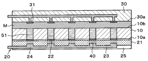
- a through hole 50 and a through electrode 51 described later are formed in the wafer 10 so as to penetrate in the thickness direction from the front surface 10 a to the back surface 10 b of the wafer 10.
- a device layer (not shown) including electronic circuits, wirings, and the like is formed on the surface 10a of the wafer 10.
- the support substrate 20 has an electrical connection between the common electrode 23 and an etching solution or a plating solution (a plurality of surface electrodes 22) as a processing solution supplied to positions where through-holes 50 and through-electrodes 51 described later are formed.
- An anisotropic conductive member (anisotropic conductive rubber) 21 is provided as a switching mechanism for switching a general connection state.
- the anisotropic conductive member 21 has, for example, a substantially disk shape, and has the same shape as that of the wafer 10 in plan view. Further, as will be described later, the anisotropic conductive member 21 is provided so as to cover the surface 10 a of the wafer 10 and to face the plurality of through electrodes 51.
- the anisotropic conductive member 21 is obtained by mixing conductive fine metal particles with an insulating resin.
- the metal particles dispersed in the pressurized portion are gathered and contacted, and the pressurized portion has a conductive path.
- the portion that has not been pressurized maintains insulation.
- anisotropy is formed that is conductive in the vertical direction and insulative in the horizontal direction.
- the anisotropic conductive member 21 may be a film or a paste, for example.
- a surface electrode 22 that can physically contact the wafer 10 and is electrically connected to the through electrode 51 is formed on the surface 21 a of the anisotropic conductive member 21, a surface electrode 22 that can physically contact the wafer 10 and is electrically connected to the through electrode 51 is formed. That is, the surface electrode 22 is formed at a position facing the formation position of the through hole 50 and the through electrode 51. Note that an insulating film is formed on the surface 21 a of the anisotropic conductive member 21 other than the surface electrode 22, so that the surface of the support substrate 20 facing the wafer 10 is a flat plane. That is, the support substrate 20 also functions as a substrate having a plane on which the wafer 10 can be mounted in the present embodiment.
- a common electrode 23 that can be electrically connected to the plurality of front surface electrodes 22 and provided in common to the plurality of through electrodes 51 is provided. As will be described later, the common electrode 23 is provided at a position facing the plurality of through electrodes 51 with the anisotropic conductive member 21 interposed therebetween.
- a protrusion 24 is formed at a position facing the surface electrode 22, that is, a position facing the formation position of the through hole 50 and the through electrode 51.
- the common electrode 23 is supported by the support member 25.
- the support substrate 20 of FIG. In order to make the electrode structure such as the internal anisotropic conductive member 21 easy to understand, the support substrate 20 of FIG. However, since the support substrate 20 is also intended to stably transport the thinned wafer 10, the support substrate 20 actually has sufficient strength and can be transported by an arm of a semiconductor manufacturing apparatus or the like. It has such a shape. The same applies to the subsequent drawings.
- the template 30 has, for example, a substantially disk shape, and has the same shape as that of the wafer 10 in plan view. Further, as will be described later, the template 30 is provided so as to cover the back surface 10 b of the wafer 10.
- silicon carbide SiC is used for the template 30.
- An electrode 31 that is electrically connected to the through electrode 51 is formed on the surface 30 a of the template 30. That is, the electrode 31 is formed at a position facing the formation position of the through hole 50 and the through electrode 51.
- the support substrate 20 is disposed on the surface 10a side of the wafer 10 (step S1 in FIG. 1).
- the support substrate 20 is disposed so as to cover the surface 10 a of the wafer 10. Further, the support substrate 20 is disposed so that the surface electrode 22 is in contact with the surface 10 a of the wafer 10 and each surface electrode 22 is opposed to the formation position of the through hole 50 and the through electrode 51.
- the bonding between the wafer 10 and the support substrate 20 is performed through an adhesive that is cured or softened according to the temperature to be heated, for example.
- step S2 the back surface 10b of the wafer 10 is polished to thin the wafer 10 to a predetermined thickness.
- the subsequent steps are performed in a state where the wafer 10 is thinned.
- the support substrate 20 gives the wafer 10 sufficient strength, it is possible to prevent the wafer 10 from being cracked during transportation. Can do.
- the template 30 is disposed on the back surface 10 side of the wafer 10, and an etching solution E as a processing solution is supplied and filled between the wafer 10 and the template 30.
- the template 30 covers the back surface 10 b of the wafer 10 and is arranged so that each electrode 31 faces the formation position of the through hole 50 and the through electrode 51.
- the etching solution E may be supplied by, for example, a separate etching solution supply device (not shown) or, for example, a flow path (not shown) of the etching solution E formed through the template 30 in the thickness direction. You may go through As the etching solution E, for example, a mixed solution of hydrofluoric acid and isopropyl alcohol (HF / IPA), a mixed solution of hydrofluoric acid and ethanol, or the like is used.
- the common electrode 23 of the support substrate 20 is pressurized and moved toward the anisotropic conductive member 21 (in the direction of the arrow in FIG. 8). Then, the anisotropic conductive member 21 is pressed by the protrusion 24 of the common substrate 23. The pressurized portion of the anisotropic conductive member 21 is compressed to form a conductive portion 40 having conductivity. On the other hand, the portion of the anisotropic conductive member 21 that is not pressurized maintains insulation. Thus, the common electrode 23 is electrically connected to the etching solution E via the conductive portion 40, the surface electrode 22, and the wafer 10.
- a voltage is applied to the etching solution E by using, for example, a power supply device (not shown) with the common electrode 23 of the support substrate 20 as a cathode and the electrode 31 of the template 30 as an anode.
- the electric field etching of the wafer 10 is performed by the etching liquid E, that is, the etching liquid E enters the wafer 10 while etching the wafer 10.
- a through hole 50 penetrating in the thickness direction is formed in the wafer 10 (step S3 in FIG. 1).
- the through hole 50 is formed, the etching solution E between the wafer 10 and the template 30 is removed.
- the through electrode 51 to be formed is made of copper, a barrier film or the like is formed inside the through hole 50 by vapor deposition or the like, if necessary.
- a plating solution M as a processing solution is supplied and filled between the wafer 10 and the template 30.
- the plating solution M may be supplied by, for example, a separate plating solution supply device (not shown), or for example, a flow path (not shown) of the plating solution M formed through the template 30 in the thickness direction. You may go through.
- the supplied plating solution M enters the through hole 50.
- an electrolytic copper plating solution is used as the plating solution M.
- the common electrode 23 of the support substrate 20 is again pressed and moved toward the anisotropic conductive member 21, that is, the conductive portion 40 is formed on the anisotropic conductive member 21, and the plating solution M and the common electrode 23 are electrically connected.
- a voltage is applied to the plating solution M by using, for example, a power supply device (not shown) with the common electrode 23 of the support substrate 20 as a cathode and the electrode 31 of the template 30 as an anode.
- electroplating is performed on the plating solution M in the through hole 50, and the through electrode 51 is formed in the through hole 50 (step S4 in FIG. 1).
- the conductive portion 40 is formed in the respective steps of electric field etching and electric field plating. However, the following electric field plating is performed while maintaining the conductive portion 40 formed when the electric field etching is performed. Also good.
- the plating solution M on the through electrode 51 is further subjected to electroplating, and bumps 52 are formed on the through electrode 51 (step S5 in FIG. 1).
- the bumps 52 are formed, the plating solution M between the wafer 10 and the template 30 is removed and the template 30 is retracted from above the wafer 10.
- the pressurization to the common electrode 23 of the support substrate 20 is stopped, and the common electrode 23 is moved to the opposite side of the anisotropic conductive member 21 (in the direction of the arrow in FIG. 13). If it does so, the pressurization of the anisotropic conductive member 21 by the projection part 24 will be stopped, and the said anisotropic conductive member 21 comes to have insulation. Thus, the common electrode 23 and the through electrode 51 (surface electrode 22) are electrically disconnected. That is, the plurality of through electrodes 51 are electrically independent.
- the inspection apparatus 60 is used to inspect the electrical characteristics of the through electrode 51 of the wafer 10 and the electronic circuit on the wafer 10 (electrical test). (Step S6 in FIG. 1).
- the inspection device 60 includes a tester 61 and a plurality of probes 62 supported on the tester 61 and having conductivity.
- the probe 62 is disposed at a position corresponding to the bump 52.
- the shape of the probe 62 is not limited to the illustrated example, and can take various shapes such as a cantilever shape.
- the inspection apparatus 60 When performing an electrical test using such an inspection apparatus 60, first, the inspection apparatus 60 is lowered to the wafer 10 side, and the probe 62 is brought into contact with the bumps 52. Subsequently, an electrical signal is sent from the tester 61 to the through electrode 51 via the probe 62 and the bump 52, and an electrical test of the through electrode 51 is performed. In addition, an electrical signal is sent from the tester 61 to the electronic circuit on the wafer 10 through the probe 62, the bump 52, and the through electrode 51, and an electrical test of the electronic circuit is performed.
- the wafer 10 and the support substrate 20 are transferred to a wafer bonding apparatus (not shown).
- a plurality of wafers 10 are transferred to the wafer bonding apparatus.
- the plurality of wafers 10 are bonded so that the through electrodes 51 and the bumps 52 of the stacked wafers 10 are electrically connected (step S ⁇ b> 7 in FIG. 1).
- the wafer 10 and the support substrate 20 are also peeled off.
- the semiconductor device 100 in which the wafers 10 are three-dimensionally stacked is manufactured.
- step S3 the anisotropic conductive member 21 is pressurized by the protrusion 24, and the electrolytic etching is performed in a state where the etching solution E and the common electrode 23 are electrically connected.
- a through hole 50 is formed in the wafer 10.
- steps S4 and S5 electrolytic plating is performed in a state where the plating solution M and the common electrode 23 are electrically connected to form a through electrode 51 in the through hole 50, and further on the through electrode 51. Bumps 52 are formed.
- step S6 the pressure applied to the anisotropic conductive member 21 by the protrusion 24 is stopped, and the through electrode 51 and the common electrode 23 are electrically disconnected, that is, the plurality of through electrodes 51 are arranged.
- the electrical characteristics of the wafer 10 are inspected while being electrically independent.
- the common electrode 23 provided in the support substrate 20 as one pole, a series of processes on the wafer 10 such as electric field plating and electric field etching can be performed.
- the support substrate 20 is also for giving sufficient strength to the thinned substrate 10, and the support substrate 20 is peeled off from the wafer 10 for processing in each device and further transfer between devices. Can be done without.
- the common electrode 23 can be electrically separated from each through electrode 51. This is because individual electronic circuits cannot be accurately inspected when the through electrodes 51 are short-circuited during inspection.
- a series of steps from the back surface polishing of the wafer 10 to the formation of the through electrode 51 and the electrical test of the electronic circuit are performed while being supported by the support substrate 20 without peeling the wafer 10 at all. Can do it.
- electric field etching is used to form the through hole 50, but plasma etching or the like may be used instead.
- Electroplating using the common electrode 23 in the support substrate 20 may be performed in the through hole 50 formed by plasma etching.
- other steps may be performed between these steps.
- the process using the common electrode 23 and the process performed in a state where each through electrode 51 is separated from the common electrode 23 are performed while the wafer 10 is held by the support substrate 20. There is a feature of.
- the bumps 52 are formed on all the through electrodes 51 in step S5.
- the bumps 52 may be selectively formed only on the predetermined through electrodes 51.
- the bump 52 is formed.
- defects in the semiconductor device are known prior to formation.
- the through electrode 51 is formed in step S4 and then the probe is brought into direct contact with the through electrode 51 and then step S6 is performed, it is possible to detect the defect of the electronic circuit and the presence or absence of the defect of the through electrode 51. It is not a problem if individual semiconductor devices are separated from the wafer 10 and only good products are stacked.
- non-defective device and a defective semiconductor device (hereinafter sometimes referred to as “defective device”) are likely to be mixed. Even when a non-defective device and a defective device are mixed in the semiconductor device 100, there is no problem if only the non-defective device is used as long as the memory devices are stacked. However, if the non-defective device and the defective device are connected in series through the through electrode 51, the entire semiconductor device 100 may be defective due to the bad influence of the defective device.
- the bump 52 is not formed on the through electrode 51 to which the defective device is connected, and the through electrode 51 of the defective device and the through electrode 51 of the non-defective device are electrically disconnected.
- the bump 52 is formed only on the through electrode 51 of the good device, and is electrically connected to the through electrode 51 of the good device and the through electrode 51 of the good device.
- the protrusion 24 is selectively formed at a position facing the through electrode 51 of the non-defective device.
- step S5 as shown in FIG. 16, the common electrode 23 is moved to the anisotropic conductive member 21 side, and the anisotropic conductive member 21 is pressurized by the protrusion 24, and the plating solution M, the common electrode 23, Are electrically connected.
- a voltage is applied to the plating solution M by using, for example, a power supply device (not shown) with the common electrode 23 as a cathode and the electrode 31 of the template 30 as an anode.
- electrolytic plating is performed on the plating solution M, and bumps 52 are selectively formed on the predetermined through electrodes 51.
- the through electrode 51 of the non-defective device is electrically connected to the through electrode 51 of another non-defective device to be laminated by the bump 52.
- the through electrode 51 of the defective device is not electrically connected to the through electrode 51 of another good device to be stacked.
- the semiconductor device 100 can be made non-defective and the yield of the semiconductor device 100 can be improved.
- each semiconductor device can only be connected in series through the through electrode 51.
- any through electrode 51 can be selected and connected from among the plurality of through electrodes 51, so that the through electrode 51 functions as a program wiring in the semiconductor device 100. It can be made.
- the bumps 52 can be formed on the arbitrary through electrodes 51 by selectively forming the protrusions 24 on the surface of the common electrode 23.
- the common electrode 23 may be exchangeable, and the common electrode 23 having the protrusions 24 necessary for each process may be selected.
- the anisotropic conductive member 21 is provided so as to cover the surface 10 a of the wafer 10, but the anisotropic conductive member 21 is located at a position facing the through electrode 51 as shown in FIG. 17. Only a plurality of them may be provided. In this case, the surface of the common electrode 23 is flat, and the protrusion 24 in the above embodiment may be omitted.
- step S4 the common electrode 23 is pressed and moved toward the anisotropic conductive member 21 as shown in FIG. Then, each anisotropic conductive member 21 is pressurized, and these anisotropic conductive members 21 have conductivity.
- a voltage is applied to the plating solution M by using, for example, a power supply device (not shown) with the common electrode 23 as a cathode and the electrode 31 of the template 30 as an anode. Then, electroplating is performed on the plating solution M in the through hole 50, and the through electrode 51 is formed in the through hole 50.
- electrolytic etching and electrolytic plating are performed by the same method, respectively.
- the same common electrode 23 is used to carry out a series of processes of electrolytic etching, electrolytic plating, and electrical testing, without being peeled off the wafer 10, and supported by the support substrate 20.
- the throughput of the manufacturing process of the semiconductor device 100 can be improved.
- the cost of the manufacturing apparatus of the semiconductor device 100 can be reduced, and the manufacturing cost of the semiconductor device 100 can also be reduced.
- the anisotropic conductive member 21 may be selectively provided at a position facing the through electrode 51 of the non-defective device as shown in FIG.
- the bump 52 is formed only on the through electrode 51 of the non-defective device. Therefore, since the defective device and the non-defective device can be electrically separated, the influence of the defective device does not reach other non-defective devices, and the yield of the semiconductor device 100 can be improved.
- step S4 when electrolytic plating is performed in step S4, the plating solution M is filled between the wafer 10 and the template 30, but the plating solution M is applied only to the through holes 50 as shown in FIG. You may make it supply.
- the flow path 150 of the plating solution M may be formed in the template 30.
- the plating solution M is supplied onto the through hole 50 through the flow passage 150.
- the back surface 10b of the wafer 10 around the through holes 50 may be hydrophobized.
- the etching solution E and the plating solution M are supplied by the same method, respectively. According to the present embodiment, since the supply amounts of the etching solution E and the plating solution M can be suppressed to a small amount, the manufacturing cost of the semiconductor device 100 can be further reduced.
- a support substrate different from the support substrate 20 of the above embodiment may be used.
- the support substrate 200 switches the electrical connection state between the common electrode 23 and the etching solution E or the plating solution M (conductive portion 202) supplied to the positions where the through holes 50 and the through electrodes 51 are formed.
- An anisotropic conductive member 201 is provided as a switching mechanism.
- the anisotropic conductive member 201 has, for example, a substantially disk shape, and has the same shape as that of the wafer 10 in plan view.
- the anisotropic conductive member 201 is provided so as to cover the surface 10 a of the wafer 10.
- the anisotropic conductive member 201 may be, for example, a film-like one or a paste-like one.
- a conductive portion 202 is formed as a surface electrode that is electrically connected to the etching solution E and the plating solution M and pressurizes the anisotropic conductive member 201.
- the conductive portion 202 is formed at a position facing the formation position of the through hole 50 and the through electrode 51.
- the conductive portion 202 may be formed on the surface 10 a of the wafer 10.
- the back surface 201b of the anisotropic conductive member 201 is provided with a support member 203 provided with a through electrode (not shown) and a common electrode 204 provided in common with the plurality of through electrodes 51.
- the common electrode 204 has the same shape as that of the wafer 10 in plan view, and is provided at a position facing the formation positions of the plurality of through electrodes 51 with the anisotropic conductive member 201 interposed therebetween. Further, the common electrode 204 is configured to be detachable from the support member 203.
- the flow path 211 of the etching solution E and the plating solution M is formed in the template 210 of the present embodiment.
- the flow path 211 penetrates the template 210 in the thickness direction, and both ends of the flow path 211 are open.
- An electrode 212 is formed on the inner surface of the flow passage 211.
- the template 210 is used in the present embodiment, the template 30 in the above embodiment may be used.
- a support substrate 200 is disposed on the surface 10a side of the wafer 10 as shown in FIG.
- the support substrate 200 is disposed so as to cover the surface 10 a of the wafer 10.
- the support substrate 200 is disposed such that the conductive portions 202 are in contact with the surface 10 a of the wafer 10, and the respective conductive portions 202 are opposed to the formation positions of the through holes 50 and the through electrodes 51.
- the conductive portion 202 pressurizes the anisotropic conductive member 201.
- the pressed portion of the anisotropic conductive member 201 is compressed to form a conductive portion 220 having conductivity.
- the portion of the anisotropic conductive member 201 that is not pressurized maintains insulation.
- step S2 the back surface 10b of the wafer 10 is polished to thin the wafer 10 to a predetermined thickness.
- a template 210 is disposed on the back surface 10 side of the wafer 10 as shown in FIG.
- the template 210 is disposed such that the flow passage 211 faces the position where the through hole 50 is formed.
- the etching solution E is supplied onto the wafer 10 through the flow path 211.
- the common electrode 204 and the etching solution E are electrically connected.
- a voltage is applied to the etching solution E by using, for example, a power supply device (not shown) with the common electrode 204 as a cathode and the electrode 212 of the template 210 as an anode.
- the electric field etching of the wafer 10 is performed by the etching solution E, and the through hole 50 is formed in the wafer 10.
- step S4 the plating solution M is supplied onto the wafer 10 through the flow path 211 as shown in FIG.
- the supplied plating solution M enters the through hole 50.
- the common electrode 204 and the plating solution M are electrically connected.
- a voltage is applied to the plating solution M by using, for example, a power supply device (not shown) with the common electrode 204 as a cathode and the electrode 212 of the template 210 as an anode.
- electroplating is performed on the plating solution M in the through hole 50, and the through electrode 51 is formed in the through hole 50.
- step S 5 electroplating is further performed on the plating solution M on the through electrode 51, and bumps 52 are formed on the through electrode 51.
- step S6 the common electrode 204 is removed from the anisotropic conductive member 201 (support member 203) as shown in FIG. 26, and the common electrode 204 and the through electrode 51 are electrically disconnected. That is, the plurality of through electrodes 51 are electrically independent. Then, using the electrode 212 of the template 210 as an electrode for an electrical test, the electrical characteristics of the through electrode 51 of the wafer 10 and the electronic circuit on the wafer 10 are inspected.
- step S7 the plurality of wafers 10 are bonded to manufacture the semiconductor device 100.
- a series of steps of electrolytic etching, electroplating, and electrical testing are supported on the support substrate 200 without peeling the wafer 10 using the same common electrode 204. This can be performed as it is, and the throughput of the manufacturing process of the semiconductor device 100 can be improved. Moreover, since the same support substrate 200 is used, the cost of the manufacturing apparatus of the semiconductor device 100 can be reduced, and the manufacturing cost of the semiconductor device 100 can also be reduced.
- the conductive portion 202 may be selectively provided at a position facing the through electrode 51 of the non-defective device as shown in FIG.
- the bump 52 is formed only on the through electrode 51 of the non-defective device. Therefore, since the defective device and the non-defective device can be electrically separated, the influence of the defective device does not reach other non-defective devices, and the yield of the semiconductor device 100 can be improved.
- the support substrate 300 includes an individual electrode layer 301, a switch layer 302, and a common electrode layer 303.
- the individual electrode layer 301, the switch layer 302, and the common electrode layer 303 are provided in this order from the wafer 10 side.
- the individual electrode layer 301 is provided with an electrode 310 as a surface electrode that is electrically connected to the through electrode 51.
- the electrode 310 is formed at a position facing the formation position of the through hole 50 and the through electrode 51.
- the switch layer 302 has a switching mechanism for switching an electrical connection state between an etching solution E or a plating solution M (electrode 310) supplied to the formation position of the through hole 50 and the through electrode 51 and a common electrode 330 described later.
- the switch circuit 320 is provided.
- the switch circuit 320 electrically connects the etching solution E or the plating solution M and the common electrode 330 in the on state, and electrically disconnects the etching solution E or the plating solution M and the common electrode 330 in the off state.
- a plurality of switch circuits 320 are provided so as to be electrically connected to each electrode 310.
- the common electrode layer 303 is provided with a common electrode 330 provided in common to the plurality of through electrodes 51. That is, the common electrode 330 is provided at a position facing the plurality of through electrodes 51 with the switch circuit 320 interposed therebetween.
- the support substrate 300 is disposed on the surface 10a side of the wafer 10.
- the support substrate 300 is disposed so as to cover the surface 10 a of the wafer 10.
- the support substrate 300 is disposed such that the electrodes 310 are in contact with the surface 10 a of the wafer 10 and the electrodes 310 are opposed to the positions where the through holes 50 and the through electrodes 51 are formed.
- step S2 the back surface 10b of the wafer 10 is polished to thin the wafer 10 to a predetermined thickness.
- step S3 the template 30 is disposed on the back surface 10 side of the wafer 10 as shown in FIG. 29, and the etching solution E is supplied and filled between the wafer 10 and the template 30.
- the template 30 covers the back surface 10 b of the wafer 10 and is arranged so that each electrode 31 faces the formation position of the through hole 50 and the through electrode 51.
- all the switch circuits 320 are turned on, and the common electrode 330 and the etching solution E are electrically connected.
- a voltage is applied to the etching solution E with the common electrode 330 as a cathode and the electrode 31 of the template 30 as an anode by a power supply device (not shown).
- the electric field etching of the wafer 10 is performed by the etching solution E, and the through hole 50 is formed in the wafer 10.
- step S4 the plating solution M is supplied and filled between the wafer 10 and the template 30 as shown in FIG.
- the supplied plating solution M enters the through hole 50.
- all the switch circuits 320 are turned on, and the common electrode 330 and the plating solution M are electrically connected.
- a voltage is applied to the plating solution M by using, for example, a power supply device (not shown) with the common electrode 330 as a cathode and the electrode 31 of the template 30 as an anode.
- electroplating is performed on the plating solution M in the through hole 50, and the through electrode 51 is formed in the through hole 50.
- step S5 electroplating is further performed on the plating solution M on the through electrode 51 to form bumps 52 on the through electrode 51.
- step S6 as shown in FIG. 32, all the switch circuits 320 are turned off, and the common electrode 330 and the through electrode 51 are disconnected. That is, the plurality of through electrodes 51 are electrically independent.
- the inspection device 60 is used to inspect the electrical characteristics of the through electrode 51 of the wafer 10 and the electronic circuit on the wafer 10. In this case, it is desirable that the switch circuit 320 is configured to be able to turn on / off all the switches at once.
- step S7 the plurality of wafers 10 are bonded to manufacture the semiconductor device 100.
- a series of steps of electrolytic etching, electrolytic plating, and electrical testing are supported on the support substrate 300 without peeling the wafer 10 using the same common electrode 330. This can be performed as it is, and the throughput of the manufacturing process of the semiconductor device 100 can be improved. Further, since the same support substrate 300 is used, the cost of the manufacturing apparatus of the semiconductor device 100 can be reduced, and the manufacturing cost of the semiconductor device 100 can also be reduced.
- the switch circuit 320 at a position facing the through electrode 51 of the non-defective device is turned on, and the through electrode of the defective device is turned on.
- the switch circuit 320 at a position facing 51 may be turned off.
- the switch circuit 320 has a function of selectively turning on / off the switch.
- the bump 52 is formed only on the through electrode 51 of the non-defective device. Accordingly, since the defective device and the non-defective device can be electrically separated, the influence of the defective device does not reach other non-defective devices, and the yield of the semiconductor device 100 can be improved.
- the support substrate 400 When performing the above wafer processing, a support substrate different from the support substrates 20, 200, and 300 of the above embodiments may be used.
- the support substrate 400 includes an individual electrode layer 401, a switch layer 402, and a liquid supply layer 403.
- the individual electrode layer 401, the switch layer 402, and the liquid supply layer 403 are provided in this order from the wafer 10 side.
- silicon or ceramics is used for the support substrate 400.
- the individual electrode layer 401 is provided with a surface electrode 410 that can physically contact the wafer 10 and is electrically connected to the through electrode 51.
- a plurality of surface electrodes 410 are formed at positions facing the formation positions of the through holes 50 and the through electrodes 51.
- an insulating film is formed on portions of the individual electrode layer 401 other than the surface electrode 410 so that the surface of the support substrate 400 facing the wafer 10 is a flat plane. That is, the support substrate 400 also functions as a substrate having a plane on which the wafer 10 can be mounted in the present embodiment.
- the switch layer 402 is formed with a space 420 capable of accommodating a conductive liquid and an insulating liquid described later. A plurality of spaces 420 are formed at positions facing the surface electrode 410.
- the liquid supply layer 403 is provided with a conductive liquid flow passage 430 for circulating a conductive liquid.
- a plurality of branch channels 431 are connected to the conductive liquid flow path 430, and each branch channel 431 is connected to the space 420.
- the conductive liquid flow passage 430 has a pressure feeding mechanism (not shown) for pumping the conductive liquid to the space 420 via the branch flow path 431, or the conductive liquid from the space 420 via the branch flow path 431. Is connected to a suction mechanism (not shown). With this configuration, the conductive liquid flow passage 430 can cause the conductive liquid to flow into each space 420 and allow the conductive liquid to flow out from each space 420.
- the conductive liquid can be caused to flow in the branch channel 431 and the space 420 by capillary action.
- the conductive liquid is stored in the space 420, the surface electrode 410 and the conductive liquid are electrically connected.
- the conductive liquid is not particularly limited as long as it is a conductive liquid.
- an electrolytic solution containing ions or a liquid metal (liquid metal) is used.
- the liquid supply layer 403 is provided with an insulating liquid flow passage 432 for circulating the insulating liquid.
- a plurality of branch flow paths 433 are connected to the insulating liquid flow path 432, and each branch flow path 433 is connected to the space 420.
- the insulating liquid flow passage 432 has a pressure feeding mechanism (not shown) for pumping the insulating liquid to the space 420 via the branch flow path 433, or the insulating liquid from the space 420 via the branch flow path 433. Is connected to a suction mechanism (not shown). With this configuration, the insulating liquid flow path 432 can allow the insulating liquid to flow into each space 420 and allow the insulating liquid to flow out from each space 420.
- the insulating liquid can be allowed to flow into the branch channel 433 and the space 420 by capillary action.
- the insulating liquid is not particularly limited as long as it is an insulating liquid. For example, pure water is used.
- the insulating liquid also functions as a cleaning liquid for the space 420 as will be described later.
- the shape of the template used in the present embodiment is not limited, but here, a case where the template 210 shown in FIG. 21 is used will be described.
- a support substrate 400 is disposed on the surface 10a side of the wafer 10 as shown in FIG.
- the support substrate 400 is disposed so as to cover the surface 10 a of the wafer 10. Further, the support substrate 400 is disposed such that the surface electrode 410 is in contact with the surface 10 a of the wafer 10 and each surface electrode 410 is opposed to the formation position of the through hole 50 and the through electrode 51.
- step S2 the back surface 10b of the wafer 10 is polished to thin the wafer 10 to a predetermined thickness.
- a template 210 is disposed on the back surface 10 side of the wafer 10 as shown in FIG.
- the template 210 is disposed such that the flow passage 211 faces the position where the through hole 50 is formed.
- the etchant E is supplied onto the wafer 10 through the flow passage 211 in a state where the periphery of the region where the through hole 50 is formed on the back surface 10b of the wafer 10 is made hydrophobic.
- the conductive liquid C is caused to flow into the space 420 from the conductive liquid flow passage 430 through the branch flow path 431, and the space 420 is filled with the conductive liquid C.
- the conductive liquid C and the etching liquid E are electrically connected.
- a voltage is applied to the etching solution E using, for example, a power supply device (not shown) using the conductive liquid C as a cathode and the electrode 212 of the template 210 as an anode. Then, the electric field etching of the wafer 10 is performed by the etching solution E, and the through hole 50 is formed in the wafer 10.
- step S4 the plating solution M is supplied onto the wafer 10 through the flow path 211 as shown in FIG.
- the supplied plating solution M enters the through hole 50.
- the space 420 is filled with the conductive liquid C from the conductive liquid flow passage 430.
- the conductive liquid C and the plating liquid M are electrically connected.
- a voltage is applied to the plating solution M by using, for example, a power supply device (not shown) with the conductive liquid C as a cathode and the electrode 212 of the template 210 as an anode.
- electroplating is performed on the plating solution M in the through hole 50, and the through electrode 51 is formed in the through hole 50.
- step S 5 electroplating is further performed on the plating solution M on the through electrode 51, and bumps 52 are formed on the through electrode 51.
- the bumps 52 are formed, the plating solution M between the wafer 10 and the template 30 is removed and the template 30 is retracted from above the wafer 10.
- step S6 the conductive liquid C is allowed to flow from the space 420 to the conductive liquid flow path 430, and then insulated from the insulating liquid flow path 432 to the space 420 via the branch flow path 433 as shown in FIG.
- a sex liquid L is introduced.
- the insulating liquid L functions as a cleaning liquid, and the space 420 is cleaned.
- the space 420 is filled with the insulating liquid L, and the conductive liquid C in the space 420 is replaced with the insulating liquid L.
- the plurality of through electrodes 51 are electrically independent.
- the electrode 212 of the template 210 as an electrode for an electrical test, the electrical characteristics of the through electrode 51 of the wafer 10 and the electronic circuit on the wafer 10 are inspected.
- step S7 the plurality of wafers 10 are bonded to manufacture the semiconductor device 100.
- a series of steps of electrolytic etching, electrolytic plating, and electrical testing can be performed. That is, a series of steps can be performed while being supported on the support substrate 400 without peeling off the wafer 10, and the throughput of the manufacturing process of the semiconductor device 100 can be improved.
- the cost of the manufacturing apparatus of the semiconductor device 100 can be reduced, and the manufacturing cost of the semiconductor device 100 can also be reduced. Therefore, according to the present embodiment, it is possible to enjoy the same effect as the above-described embodiment.
- the support substrate 400 has substantially the same structure as the template 210, does not require a common electrode as in the above embodiment, and it is sufficient that the space 420 is formed in the switch layer 402. Therefore, the structure of the support substrate 400 can be simplified, and the cost of the manufacturing apparatus for the semiconductor device 100 can be further reduced.
- the conductive liquid C or the insulating liquid L may be selectively filled in the plurality of spaces 420 as shown in FIG.
- the conductive liquid C is filled in the space 420 facing the through electrode 51 of the non-defective device
- the insulating liquid L is filled in the remaining space 420, that is, the space 420 corresponding to the defective device.
- the bump 52 is formed only on the through electrode 51 of the non-defective device. Accordingly, since the defective device and the non-defective device can be electrically separated, the influence of the defective device does not reach other non-defective devices, and the yield of the semiconductor device 100 can be improved.
- the conductive liquid flow passage 430 and the insulating liquid flow passage 432 are provided in the liquid supply layer 403 of the support substrate 400.
- the cleaning liquid flow passage 440 may be provided.
- a plurality of branch flow paths 441 are connected to the cleaning liquid flow passage 440, and each branch flow path 441 is connected to the space 420.
- the cleaning liquid flow passage 440 includes a pressure feeding mechanism (not shown) for pumping the cleaning liquid to the space 420 via the branch flow path 441, and the cleaning liquid from the space 420 via the branch flow path 441.
- a suction mechanism (not shown) for sucking the water is provided.
- the cleaning liquid flow passage 440 can allow the cleaning liquid to flow into each space 420 and allow the cleaning liquid to flow out from each space 420.
- the cleaning liquid flows in the branch channel 441 and the space 420 by capillary action.
- the cleaning liquid flow path 440 passes through the branch flow path 441 and is used for cleaning in the space 420. Let the liquid flow in. Then, the space 420 is cleaned with a cleaning liquid. Thereafter, the cleaning liquid is allowed to flow from the space 420 to the cleaning liquid flow path 440, and then the insulating liquid L is allowed to flow from the insulating liquid flow path 432 to the space 420. Thus, the conductive liquid C in the space 420 is replaced with the insulating liquid L.
- the space 420 is cleaned with a cleaning liquid different from the insulating liquid L, the conductive liquid C can be more reliably removed from the space 420 and the space 420 can be cleaned. it can. Therefore, the electrical test performed thereafter can be performed more appropriately.
- the conductive liquid flow passage 430 and the insulating liquid flow passage 432 are provided in the liquid supply layer 403 of the support substrate 400.
- the conductive liquid flow passage 430 and the insulating liquid flow passage 432 are provided.
- a liquid flow passage 450 through which the conductive liquid C or the insulating liquid L flows may be provided.
- a plurality of branch channels 451 are connected to the liquid flow passage 450, and each branch channel 451 is connected to the space 420.
- the liquid flow passage 450 has a pressure feeding mechanism (not shown) for pressure-feeding the conductive liquid C or the insulating liquid L to the space 420 via the branch flow path 451, and the space 420 via the branch flow path 451.
- a suction mechanism (not shown) for sucking the conductive liquid C or the insulating liquid L is provided.
- the liquid flow passage 450 can cause the conductive liquid C or the insulating liquid L to flow into each space 420 and allow the conductive liquid C or the insulating liquid L to flow out from each space 420. Further, since the diameters of the branch flow path 451 and the space 420 are small, the conductive liquid C or the insulating liquid L flows in the branch flow path 451 and the space 420 by capillary action.
- step S3 to S5 the space 420 can be filled with the conductive liquid C to perform electrolytic etching and electroplating, and in step S6, the space 420 can be filled with the insulating liquid L to electrically A test can be performed. That is, by replacing the conductive liquid C and the insulating liquid L in the space 420, a series of steps of electrolytic etching, electrolytic plating, and electrical test can be performed on the support substrate 400 without peeling the wafer 10 once. This can be performed while being supported, and the throughput of the manufacturing process of the semiconductor device 100 can be improved.
- the cost of the manufacturing apparatus of the semiconductor device 100 can be reduced, and the manufacturing cost of the semiconductor device 100 can also be reduced. Therefore, according to the present embodiment, it is possible to enjoy the same effect as the above-described embodiment.
- the liquid supply system is one system (liquid flow passage 450)
- the structure of the support substrate 400 can be further simplified, and the cost of the manufacturing apparatus of the semiconductor device 100 can be further reduced.
- a cleaning liquid for cleaning the space 420 may be further circulated in the liquid flow passage 450.
- the support substrate 400 in the above embodiment has a three-layer structure of the individual electrode layer 401, the switch layer 402, and the liquid supply layer 403. However, as shown in FIG. It may be a substrate on which 460 is formed.
- a plurality of permeation holes 461 are formed on the upper surface of the support substrate 400. Each penetration hole 461 is provided with the surface electrode 410 described above that can physically contact the wafer 10 and is electrically connected to the through electrode 51.
- an inflow hole 462 through which the conductive liquid C or the insulating liquid L flows into the space 460 and an outflow hole 463 through which the conductive liquid C and the insulating liquid L flow out from the space 460 are formed on the upper surface of the support substrate 400.
- the inflow hole 462 is connected to a conductive liquid flow path (not shown) for flowing the conductive liquid C and an insulating liquid flow path (not shown) for flowing the insulating liquid L. ing.
- a conductive liquid flow passage (not shown) and an insulating liquid flow passage (not shown) are connected to the outflow hole 463.
- the space 460 can be filled with the conductive liquid C to perform electrolytic etching and electroplating, and in step S6, the space 460 can be filled with the insulating liquid L to electrically A test can be performed. That is, by replacing the conductive liquid C and the insulating liquid L in the space 460, a series of steps of electrolytic etching, electrolytic plating, and electrical testing can be performed on the support substrate 400 without removing the wafer 10 even once. This can be performed while being supported, and the throughput of the manufacturing process of the semiconductor device 100 can be improved.
- the cost of the manufacturing apparatus of the semiconductor device 100 can be reduced, and the manufacturing cost of the semiconductor device 100 can also be reduced. Therefore, according to the present embodiment, it is possible to enjoy the same effect as the above-described embodiment.
- a cleaning liquid for cleaning the space 460 may be circulated in the space 460.
- the spaces 420 and 460 are filled with the insulating liquid L in the electrical test of step S6.
- the spaces 420 and 460 are not filled with the liquid, that is, air is filled. Good.
- the plurality of through electrodes 51 can be electrically independent to appropriately perform an electrical test.
- the through electrode 51 is formed in step S4.
- the through electrode 51 is formed between the step S3 and step S4, that is, in the through hole 50.
- An electrodeposition insulating film is formed on the inner side surface of the through hole 50 before the formation.
- the electrodeposition insulating film may be formed using the method of the present invention. In the following description, description will be made using the support substrate 400 and the template 210, but other support substrates 20, 200, 300, or other templates 30 may be used.
- an electrodeposition insulating film solution for example, an electrodeposition polyimide solution
- an electrodeposition insulating film solution is supplied onto the wafer 10 through the flow path 211 of the template 210.
- the supply of the electrodeposition insulating film solution is the same as that in which the plating solution M shown in FIG.
- the electrodeposition insulating film solution supplied on the wafer 10 enters the through hole 50.
- the space 420 is filled with the conductive liquid C from the conductive liquid flow passage 430.
- a voltage is applied to the electrodeposition insulating film solution by using, for example, a power supply device (not shown) using the conductive liquid C as a cathode and the electrode 212 of the template 210 as an anode.
- an electrodeposition insulating film having a uniform film thickness for example, an electrodeposition polyimide film, is formed on the inner side surface of the through hole 50.
- the electrodeposited polyimide film thus formed functions as an insulating film between the wafer 10 as a conductor and the through electrode 51.
- an insulating film has been formed on the inner surface of the through hole 50 by vapor deposition polymerization, CVD, or the like.
- CVD vapor deposition polymerization
- the film grows uniformly, an insulating film that grows between the wafer and the supporting substrate has been a problem. No problem occurs.
- the template 210 and the support substrate 400 used in step S4 and the like can be used, the cost is reduced.
- the electrodeposition insulating film is also formed on the bottom of the through hole 50 on the support substrate 400 side.
- the electrodeposition insulating film on the bottom using laser processing, dry etching, or the like. May be selectively removed.
- the support substrates 20, 200, 300, and 400 described in the embodiments so far are for temporarily holding the wafer 10
- the support substrates may be used as they are as an interposer.
- the interposer mainly relays between a chip having a different terminal pitch and the main board. Inside the support substrate, a switch circuit and the like as described above in the present invention and a wiring layer connected to the main substrate are formed. In this case, the wafer is not finally peeled off from the support substrate. After a plurality of wafers are stacked on the support substrate, the wafer is diced together with the support substrate. The singulated support substrate functions as an interposer.
Landscapes
- Engineering & Computer Science (AREA)
- Microelectronics & Electronic Packaging (AREA)
- Power Engineering (AREA)
- Manufacturing & Machinery (AREA)
- Computer Hardware Design (AREA)
- Physics & Mathematics (AREA)
- General Physics & Mathematics (AREA)
- Condensed Matter Physics & Semiconductors (AREA)
- Chemical & Material Sciences (AREA)
- Chemical Kinetics & Catalysis (AREA)
- Metallurgy (AREA)
- Electrochemistry (AREA)
- Materials Engineering (AREA)
- Organic Chemistry (AREA)
- Life Sciences & Earth Sciences (AREA)
- Sustainable Development (AREA)
- General Chemical & Material Sciences (AREA)
- Testing Or Measuring Of Semiconductors Or The Like (AREA)
- Internal Circuitry In Semiconductor Integrated Circuit Devices (AREA)
Abstract
被処理基板を支持するための支持基板は、前記被処理基板を搭載することのできる平面を有する基板と、前記基板の表面に露出し、前記被処理基板に物理的に接触可能な複数の表面電極と、前記複数の表面電極に電気的に接続可能な共通電極と、前記複数の表面電極と前記共通電極との電気的な接続状態を切り替えるための切替機構と、を有する。前記切替機構は異方性導電部材を有し、前記共通電極の異方性導電部材側の表面には、前記表面電極に対向する位置に突起部が形成されている。
Description
本発明は、被処理基板を支持するための支持基板、及び当該支持基板に支持された被処理基板に所定の処理を行う基板の処理方法に関する。
近年、半導体装置の高性能化が要求され、半導体デバイスの高集積化が進んでいる。かかる状況下で、高集積化された半導体デバイスを水平面内に複数配置し、これら半導体デバイスを配線で接続して半導体装置を製造する場合、配線長が増大し、それにより配線の抵抗が大きくなること、また配線遅延が大きくなることが懸念される。
そこで、半導体デバイスを3次元に積層する3次元集積技術が提案されている。この3次元集積技術においては、裏面を研磨することで薄化され、表面に複数の電子回路が形成された半導体ウェハ(以下、「ウェハ」という)を貫通するように、例えば100μm以下の微細な径を有する電極、いわゆる貫通電極(TSV:Through Silicon Via)が複数形成される。そして、この貫通電極を介して、上下に積層されたウェハが電気的に接続される(特許文献1)。
上述した貫通電極を形成する方式には、様々なものが検討されている。そのうちの一つの形式として、電子回路の形成されていないウェハ裏面を研磨してウェハを所定の厚みに薄化した後、ウェハに貫通孔を形成し、当該貫通孔内にバリア膜や貫通電極を形成するものがある。この貫通孔には高い位置精度が求められるため、貫通孔の形成にあたっては、フォトリソグラフィー技術によりマスクを形成し、マスクが形成されたウェハをプラズマエッチング処理などのいわゆるドライエッチング技術を用いてエッチングを行うことで貫通孔が形成される。当該貫通孔内に蒸着方法などによりバリア膜を形成した後、スパッタリング、めっきなどにより金属を埋め込むことで貫通電極が形成される。ここで、ウェハ裏面を研磨する工程はバックグラインドと呼ばれ、一般的にはウェハが100μm程度の厚さになるまで研磨される。しかし、ウェハが薄くなると、割れやすくなったり、搬送が困難になったりするので、研磨工程の前にウェハ表面に支持基板が張り付けられ、その後の一連の工程が行われる。
さらに、半導体装置の製造工程においては、上述したように貫通電極を形成した後、ウェハの貫通電極や電子回路等の電気的試験が行われる。この電気的試験は、例えばテスタや、プローブカード、ウェハを載置する載置台などを有するプローブ装置を用いて行われる。そして、例えばプローブカードに設けられたプローブピンをウェハ上の電極に接触させた状態で、テスタからプローブカードを介して各電極に電気信号が送信されて、ウェハの貫通電極や電子回路等の電気的試験が行われている(特許文献2)。
しかしながら、上述のように半導体装置を製造する際、ウェハに貫通電極を形成する貫通電極形成工程、ウェハの貫通電極や電子回路等の電気的試験を行うプロービング工程が別々の装置で行われているため、これら装置間でウェハの搬送を行う必要がある。このため、半導体装置の製造工程のスループットに改善の余地があった。
そこで、半導体装置の製造工程のスループットを改善するため、発明者らは、貫通孔形成工程を電解エッチングで行い、貫通電極形成工程を電解めっきで行うことを検討した。このように電界エッチングと電界めっきを行うためには、電界を形成するための電極と対向電極が必要となるが、電界エッチングと電界めっきを行う際の電極と対向電極を共通にし、貫通孔形成工程と貫通電極形成工程を連続して行うことを検討した。かかる場合では、例えば対向電極はすべての貫通電極に対して共通の電極となるため、この状態でウェハの貫通電極や電子回路等の電気的試験を行おうとすると、すべての貫通電極がショートした状態となり電気的試験を行うことができない。このため、プロービング工程では、対向電極を取り外す等の工程が別途必要となる。したがって、半導体装置の製造工程のスループットを改善するには至らなかった。
本発明は、かかる点に鑑みてなされたものであり、半導体装置の製造工程のスループットを向上させることを目的とする。
前記の目的を達成するため、本発明は、被処理基板を支持するための支持基板であって、前記被処理基板を搭載することのできる平面を有する基板と、前記基板の表面に露出し、前記被処理基板に物理的に接触可能な複数の表面電極と、前記複数の表面電極に電気的に接続可能な共通電極と、を有する。
本発明によれば、支持基板が表面電極と共通電極を有しており、表面電極と共通電極を電気的に接続することができる。そうすると、例えば支持基板に被処理基板を搭載した状態で、当該被処理基板の表面に処理液を供給した後、表面電極を通じて処理液と共通電極とを電気的に接続した状態で、当該処理液によって被処理基板に所定の処理を行うことができる。このように、支持基板に設けられた共通電極を一方の極とすることで、被処理基板に対する一連の処理を行うことができる。またその後、例えば処理液と共通電極とを電気的に非接続にした状態で、被処理基板の電気的特性の検査を行うこともできる。換言すれば、支持基板は薄化された被処理基板に十分な強度を与えるために用いられつつ、この支持基板が表面電極と共通電極を有していることにより、支持基板を被処理基板から剥離することなく、支持基板に支持された状態のまま、被処理基板に対する処理と電気的特性の検査を行うことができるのである。したがって、半導体装置の製造工程のスループットを向上させることができる。しかも、同一の支持基板を用いて基板の所定の処理と電気的特性の検査を行うことができるので、半導体装置の製造装置のコストを低廉化することができ、当該半導体装置の製造コストも低廉化することができる。
別な観点による本発明は、被処理基板に所定の処理を行う基板の処理方法であって、複数の表面電極と、前記複数の表面電極に電気的に接続可能な共通電極とを備えた支持基板に、被処理基板を搭載する基板搭載工程と、その後、前記被処理基板の表面に処理液を供給した後、前記複数の表面電極を通じて前記処理液と前記共通電極とを電気的に接続した状態で、前記処理液によって前記被処理基板に所定の処理を行う処理工程と、を有する。
別な観点による本発明は、被処理基板を支持するための支持基板であって、前記被処理基板を搭載することのできる平面を有する基板と、前記基板の表面に露出し、前記被処理基板に物理的に接触可能な複数の表面電極と、前記基板の内部に設けられ、前記複数の表面電極に電気的に接続される導電性液を収容可能な空間と、を有する。
別な観点による本発明は、被処理基板に所定の処理を行う基板の処理方法であって、複数の表面電極と、前記複数の表面電極に電気的に接続される導電性液を収容可能な空間とを備えた支持基板に、被処理基板を搭載する基板搭載工程と、その後、前記空間に前記導電性液を流入させ、前記被処理基板の表面に処理液を供給した後、前記複数の表面電極を通じて前記処理液と前記導電性液とを電気的に接続した状態で、前記処理液によって前記被処理基板に所定の処理を行う処理工程と、を有する。
本発明によれば、半導体装置の製造工程のスループットを向上させることができる。
以下、本発明の実施の形態について説明する。本実施の形態では、本発明にかかる被処理基板としてのウェハの処理方法について、当該ウェハ処理で用いられるウェハ、支持基板、及びテンプレートの構成と共に説明する。図1は、本実施の形態にかかるウェハ処理の主な処理フローを示している。なお、以下の説明で用いる図面において、各構成要素の寸法は、技術の理解の容易さを優先させるため、必ずしも実際の寸法に対応していない。
先ず、本実施の形態のウェハ処理で用いられるウェハ、支持基板、及びテンプレートの構成について説明する。図2に示すようにウェハ10には、ウェハ10の表面10aから裏面10bまで厚み方向に貫通する、後述する貫通孔50と貫通電極51が形成される。なお、ウェハ10の表面10aには、電子回路や配線等を含むデバイス層(図示せず)が形成されている。
図3に示すように支持基板20は、後述する貫通孔50と貫通電極51の形成位置に供給される処理液としてのエッチング液やめっき液(複数の表面電極22)と共通電極23との電気的な接続状態を切り替えるための切替機構としての異方性導電部材(異方性導電ゴム)21を有している。異方性導電部材21は、例えば略円盤形状を有し、ウェハ10の平面視における形状と同一の形状を有している。また、後述するように異方性導電部材21は、ウェハ10の表面10aを覆い、複数の貫通電極51に対向するように設けられる。異方性導電部材21は、絶縁性の樹脂に導電性の微細な金属粒子を混合したものである。そして、異方性導電部材21の所定の部分が加圧されると、加圧された部分において分散していた金属粒子が集合して接触し、当該加圧された部分が導電性を有する経路を形成する。一方、加圧されなかった部分における金属粒子は分散した状態であるため、当該加圧されなかった部分は絶縁性を維持する。こうして異方性導電部材21では、縦方向には導電性で横方向には絶縁性が保持される異方性が形成される。なお、異方性導電部材21には、例えばフィルム状のものを用いてもよいし、ペースト状のものを用いてもよい。
異方性導電部材21の表面21aには、ウェハ10に物理的に接触可能であり、且つ貫通電極51に電気的に接続される表面電極22が形成されている。すなわち、表面電極22は、貫通孔50と貫通電極51の形成位置に対向する位置に形成されている。なお、異方性導電部材21の表面21aにおいて、表面電極22以外の部分には絶縁膜を形成することで、支持基板20のウェハ10に対向する表面は平坦な平面になっている。すなわち、支持基板20は、本実施の形態においてウェハ10を搭載することのできる平面を有する基板としても機能している。
異方性導電部材21の裏面21bには、複数の表面電極22に電気的に接続可能であり、且つ複数の貫通電極51に共通して設けられた共通電極23が設けられている。共通電極23は、後述するように異方性導電部材21を挟んで複数の貫通電極51に対向する位置に設けられる。共通電極23の異方性導電部材21側の表面には、表面電極22に対向する位置、すなわち貫通孔50と貫通電極51の形成位置に対向する位置に突起部24が形成されている。また、共通電極23は、支持部材25によって支持されている。なお、内部の異方性導電部材21などの電極構造を分かりやすくするため、図3の支持基板20は簡略化して描いている。しかし、支持基板20は薄化されたウェハ10を安定して搬送することが目的でもあるから、実際には支持基板20は全体として十分な強度を有し、半導体製造装置のアームなどによって搬送できるような形状を有している。これはその後の図においても同様である。
図4に示すようにテンプレート30は、例えば略円盤形状を有し、ウェハ10の平面視における形状と同一の形状を有している。また、後述するようにテンプレート30は、ウェハ10の裏面10bを覆うように設けられている。テンプレート30には、例えば炭化珪素(SiC)などが用いられる。
テンプレート30の表面30aには、貫通電極51に電気的に接続される電極31が形成されている。すなわち、電極31は、貫通孔50と貫通電極51の形成位置に対向する位置に形成されている。
次に、以上のように構成されたウェハ10、支持基板20、及びテンプレート30を用いたウェハ処理について説明する。
先ず、図5に示すようにウェハ10の表面10a側に支持基板20が配設される(図1の工程S1)。支持基板20は、ウェハ10の表面10aを覆うように配置される。また、支持基板20は、表面電極22がウェハ10の表面10aに接し、且つ各表面電極22が貫通孔50と貫通電極51の形成位置に対向するように配置される。なお、ウェハ10と支持基板20の接合は、例えば加熱する温度に応じて硬化又は軟化する接着剤を介して行われる。
その後、図6に示すようにウェハ10の裏面10bを研磨し、ウェハ10を所定の厚みに薄化する(図1の工程S2)。この工程S2の後は、ウェハ10が薄化された状態で後続の工程が行われるが、支持基板20がウェハ10に十分な強度を与えるので、搬送時のウェハ10の割れなどを防止することができる。
その後、図7に示すようにウェハ10の裏面10側にテンプレート30を配設すると共に、ウェハ10とテンプレート30の間に処理液としてのエッチング液Eを供給して充填する。テンプレート30は、ウェハ10の裏面10bを覆い、且つ各電極31が貫通孔50と貫通電極51の形成位置に対向するように配置される。また、エッチング液Eの供給は、例えば別途のエッチング液供給装置(図示せず)によって行ってもよいし、例えばテンプレート30に厚み方向に貫通して形成されたエッチング液Eの流通路(図示せず)を介して行ってもよい。なお、エッチング液Eとしては、例えばフッ酸とイソプロピルアルコールの混合液(HF/IPA)やフッ酸とエタノールの混合液などが用いられる。
その後、図8に示すように支持基板20の共通電極23を異方性導電部材21側(図8の矢印の方向)に加圧して移動させる。そうすると、共通基板23の突起部24によって異方性導電部材21が加圧される。加圧された部分の異方性導電部材21は、圧縮されて導電性を有する導電部40が形成される。一方、加圧されていない部分の異方性導電部材21は、絶縁性を維持している。こうして共通電極23は、導電部40、表面電極22、ウェハ10を介して、エッチング液Eと電気的に接続される。
その後、例えば電源装置(図示せず)により、支持基板20の共通電極23を陰極とし、テンプレート30の電極31を陽極として、エッチング液Eに電圧を印加する。そうすると、エッチング液Eによってウェハ10の電界エッチングが行われ、すなわちエッチング液Eがウェハ10をエッチングしながら当該ウェハ10の内部に進入する。そして、図9に示すようにウェハ10に厚み方向に貫通する貫通孔50が形成される(図1の工程S3)。貫通孔50が形成されると、ウェハ10とテンプレート30の間のエッチング液Eが除去される。形成される貫通電極51が銅からなる場合は、必要に応じて、貫通孔50内部にはバリア膜などが蒸着などにより形成される。
その後、図10に示すようにウェハ10とテンプレート30の間に処理液としてのめっき液Mを供給して充填する。めっき液Mの供給は、例えば別途のめっき液供給装置(図示せず)によって行ってもよいし、例えばテンプレート30に厚み方向に貫通して形成されためっき液Mの流通路(図示せず)を介して行ってもよい。そして、供給されためっき液Mは、貫通孔50内に進入する。なお、めっき液Mとしては、例えば電解銅めっき液などが用いられる。
その後、図11に示すように、再び支持基板20の共通電極23を異方性導電部材21側に加圧して移動させ、すなわち異方性導電部材21に導電部40を形成して、めっき液Mと共通電極23とを電気的に接続する。この状態で、例えば電源装置(図示せず)により、支持基板20の共通電極23を陰極とし、テンプレート30の電極31を陽極として、めっき液Mに電圧を印加する。そして、貫通孔50内のめっき液Mに対して電界めっきが行われ、当該貫通孔50内に貫通電極51が形成される(図1の工程S4)。なお、本実施の形態においては、電界エッチングと電界めっきとそれぞれの工程で導電部40を形成したが、電界エッチングをした際に形成した導電部40を維持したまま、次の電界めっきを行ってもよい。
その後、図12に示すように貫通電極51上のめっき液Mに対してさらに電界めっきが行われ、当該貫通電極51上にバンプ52が形成される(図1の工程S5)。バンプ52が形成されると、ウェハ10とテンプレート30の間のめっき液Mが除去されると共に、テンプレート30をウェハ10の上方から退避させる。
その後、図13に示すように支持基板20の共通電極23への加圧を停止し、共通電極23を異方性導電部材21の反対側(図13の矢印の方向)に移動させる。そうすると、突起部24による異方性導電部材21の加圧が停止され、当該異方性導電部材21は絶縁性を有するようになる。こうして共通電極23と貫通電極51(表面電極22)とは、電気的に非接続の状態になる。すなわち、複数の貫通電極51は電気的に独立した状態になる。
共通電極23と貫通電極51とを電気的に非接続にした状態で、検査装置60を用いて、ウェハ10の貫通電極51やウェハ10上の電子回路等の電気的特性の検査(電気的試験)を行う(図1の工程S6)。検査装置60は、テスタ61と、当該テスタ61上に支持され、導電性を有する複数のプローブ62とを有している。プローブ62は、バンプ52に対応する位置に配置されている。なお、プローブ62の形状は、図示の例に限定されず、例えばカンチレバー形状等、種々の形状を取り得ることができる。
かかる検査装置60を用いて電気的試験を行う際には、先ず、検査装置60をウェハ10側に下降させて、プローブ62をバンプ52に接触させる。続いて、テスタ61からプローブ62、バンプ52を介して貫通電極51に電気信号が送られ、貫通電極51の電気的試験が行われる。また、テスタ61からプローブ62、バンプ52、貫通電極51を介してウェハ10上の電子回路に電気信号が送られ、電子回路の電気的試験が行われる。
その後、ウェハ10と支持基板20は、ウェハ接合装置(図示せず)に搬送される。ウェハ接合装置には、複数のウェハ10が複数搬送される。そして、図14に示すように積層されるウェハ10の貫通電極51とバンプ52が導通するように複数のウェハ10が接合される(図1の工程S7)。なお、この工程S7では、ウェハ10と支持基板20の剥離も行われる。こうしてウェハ10が3次元的に積層された半導体装置100が製造される。
以上の実施の形態によれば、工程S3において、異方性導電部材21を突起部24によって加圧し、エッチング液Eと共通電極23とを電気的に接続した状態で電解エッチングが行われて、ウェハ10に貫通孔50が形成される。また、工程S4と工程S5において、めっき液Mと共通電極23とが電気的に接続された状態で電解めっきが行われて、貫通孔50に貫通電極51が形成され、さらに貫通電極51上にバンプ52が形成される。その後、工程S6において、異方性導電部材21への突起部24による加圧を停止し、貫通電極51と共通電極23とを電気的に非接続にした状態で、すなわち複数の貫通電極51を電気的に独立させた状態で、ウェハ10の電気的特性の検査が行われる。このように、支持基板20内に設けられた共通電極23を一方の極とすることで、電界めっきや電界エッチングなどのウェハ10に対する一連の処理を行うことができる。先述したように、支持基板20は薄化された基板10に十分な強度を与える為のものでもあり、個々の装置における処理、さらには装置間の搬送を、支持基板20をウェハ10から剥がすことなく行うことができる。さらに、バンプ52、貫通電極51を介してウェハ10上の電子回路を検査する際には、共通電極23を各貫通電極51から電気的に分離した状態にすることもできる。検査時には各貫通電極51が短絡した状態では、個々の電子回路を正確に検査することができないからである。したがって、ウェハ10の裏面研磨から貫通電極51の形成、及び電子回路の電気的試験までの一連の工程を、一度もウェハ10を剥離することなく、支持基板20に支持された状態のまま行うことができるのである。なお、本実施の形態においては、貫通孔50の形成において電界エッチングを用いたが、プラズマエッチングなどに代えても構わない。プラズマエッチングにより形成された貫通孔50内に、支持基板20内の共通電極23を利用した電界めっきを行ってもよい。また、これらの工程の間に他の工程が行われても構わない。要するに、共通電極23を利用した工程と、各貫通電極51が共通電極23から分離された状態で行われる工程とが、ウェハ10を支持基板20で保持した状態で行われることに本実施の形態の特徴があるのである。
以上の実施の形態では、工程S5においてすべての貫通電極51上にバンプ52を形成したが、所定の貫通電極51上にのみ選択的にバンプ52を形成するようにしてもよい。
ここで、例えば工程S4において形成した複数の貫通電極51のうち、貫通電極51に欠陥がある場合や、貫通電極51に接続される半導体デバイスの電子回路が不良品である場合など、バンプ52を形成する前に半導体デバイスの欠陥が分かっている場合がある。或いは、工程S4で貫通電極51を形成した後、貫通電極51に直接プローブをコンタクトさせて工程S6を行えば、電子回路の不良や貫通電極51の欠陥の有無を検出することができる。ウェハ10から各半導体デバイスを個片化し、良品のみを積層するのであれば問題にはならないが、生産効率を向上させる為、ウェハレベルで積層していくと、半導体装置100中に良品の半導体デバイス(以下、「良品デバイス」と呼ぶ場合がある。)と、不良品の半導体デバイス(以下、「不良品デバイス」と呼ぶ場合がある。)とが混在する確率が高くなってしまう。半導体装置100の中に、良品デバイスと不良品デバイスとが混在する場合であっても、メモリデバイスの積層であれば、良品デバイスのみを使用するようにすれば問題にはならない。しかし、良品デバイスと不良品デバイスとが貫通電極51を通じて直列に接続されると、不良品デバイスの悪影響を受けて半導体装置100全体が不良品になってしまう恐れがある。そこで、不良品デバイスを他の良品デバイスから電気的に分離する必要がある。すなわち、不良品デバイスが接続される貫通電極51上にバンプ52を形成せず、不良品デバイスの貫通電極51と良品デバイスの貫通電極51と電気的に非接続にする。一方、良品デバイスの貫通電極51上にのみバンプ52を形成して、良品デバイスの貫通電極51と良品デバイスの貫通電極51と電気的に接続する。
そこで本実施の形態では、図15に示すように支持基板20の共通電極23の表面において、良品デバイスの貫通電極51に対向する位置に選択的に突起部24が形成される。そして、工程S5において、図16に示すように共通電極23を異方性導電部材21側に移動させて、突起部24によって異方性導電部材21を加圧し、めっき液Mと共通電極23とを電気的に接続する。この状態で、例えば電源装置(図示せず)により、共通電極23を陰極とし、テンプレート30の電極31を陽極として、めっき液Mに電圧を印加する。そして、めっき液Mに対して電解めっきが行われ、所定の貫通電極51上にバンプ52が選択的に形成される。
本実施の形態によれば、良品デバイスの貫通電極51のみが、バンプ52によって、積層される他の良品デバイスの貫通電極51と電気的に接続される。一方、不良品デバイスの貫通電極51は、積層される他の良品デバイスの貫通電極51と電気的に接続されない。このように不良品デバイスと良品デバイスが電気的に分離されるので、不良品デバイスの影響が他の良品デバイスに及ばない。したがって、不良品デバイスが存在しても半導体装置100を良品にすることができ、半導体装置100の歩留まりを向上させることができる。
或いは、同様にバンプ52を選択的に形成することにより、積層される半導体デバイス間の接続を各チップ間で変えることも可能である。これまでの3次元集積技術では、各半導体デバイスは貫通電極51を通じて直列に接続されるしかなかった。しかし、本実施の形態を利用すれば、複数の貫通電極51のうちから任意の貫通電極51を選択して接続させることができるようになるので、貫通電極51を半導体装置100におけるプログラム配線として機能させることができるのである。このように、共通電極23の表面において選択的に突起部24を形成することで、任意の貫通電極51上にバンプ52を形成することができる。共通電極23を交換可能にしておき、各工程で必要な突起部24を有する共通電極23を選択するようにすればよい。
以上の実施の形態では、異方性導電部材21はウェハ10の表面10aを覆うように設けられていたが、図17に示すように異方性導電部材21は貫通電極51に対向する位置にのみ複数設けられていてもよい。かかる場合、共通電極23の表面は平坦であって、上記実施の形態における突起部24を省略してもよい。
そして、例えば工程S4において、図18に示すように共通電極23を異方性導電部材21側に加圧して移動させる。そうすると、各異方性導電部材21がそれぞれ加圧され、これら異方性導電部材21が導電性を有するようになる。この状態で、例えば電源装置(図示せず)により、共通電極23を陰極とし、テンプレート30の電極31を陽極として、めっき液Mに電圧を印加する。そして、貫通孔50内のめっき液Mに対して電界めっきが行われ、当該貫通孔50内に貫通電極51が形成される。なお、工程S3や工程S5においても、同様の方法で電解エッチングと電解めっきがそれぞれ行われる。
本実施の形態によっても、同一の共通電極23を用いて、電解エッチング、電解めっき、及び電気的試験の一連の工程を、一度もウェハ10を剥離することなく、支持基板20に支持された状態のままで行うことができ、半導体装置100の製造工程のスループットを向上させることができる。また、同一の支持基板20を用いているので、半導体装置100の製造装置のコストを低廉化することができ、当該半導体装置100の製造コストも低廉化することができる。
また、本実施の形態においても、図19に示すように良品デバイスの貫通電極51に対向する位置に選択的に異方性導電部材21を設けてもよい。かかる場合、良品デバイスの貫通電極51上にのみバンプ52が形成される。したがって、不良品デバイスと良品デバイスを電気的に分離できるので、不良品デバイスの影響が他の良品デバイスに及ばず、半導体装置100の歩留まりを向上させることができる。
以上の実施の形態では、工程S4において電解めっきを行う際、ウェハ10とテンプレート30の間にめっき液Mを充填していたが、図20に示すように貫通孔50上にのみめっき液Mを供給するようにしてもよい。かかる場合、例えばテンプレート30にめっき液Mの流通路150が形成されていてもよい。そして、流通路150を介して貫通孔50上にめっき液Mが供給される。また、貫通孔50上のみにめっき液Mを供給するため、貫通孔50の周囲のウェハ10の裏面10bを疎水化してもよい。なお、工程S3や工程S5においても、同様の方法でエッチング液Eとめっき液Mがそれぞれ供給される。本実施の形態によれば、エッチング液Eとめっき液Mの供給量を少量に抑えることができるので、半導体装置100の製造コストをさらに低廉化することができる。
以上のウェハ処理を行うに際しては、以上の実施の形態の支持基板20と異なる支持基板を用いてもよい。図21に示すように支持基板200は、貫通孔50と貫通電極51の形成位置に供給されるエッチング液Eやめっき液M(導電部202)と共通電極23との電気的な接続状態を切り替えるための切替機構としての異方性導電部材201を有している。異方性導電部材201は、例えば略円盤形状を有し、ウェハ10の平面視における形状と同一の形状を有している。また、異方性導電部材201は、ウェハ10の表面10aを覆うように設けられる。なお、異方性導電部材201には、例えばフィルム状のものを用いてもよいし、ペースト状のものを用いてもよい。
異方性導電部材201の表面201aには、エッチング液Eやめっき液Mと電気的に接続され、且つ異方性導電部材201を加圧する表面電極としての導電部202が形成されている。導電部202は、貫通孔50と貫通電極51の形成位置に対向する位置に形成されている。なお、この導電部202は、ウェハ10の表面10aに形成されていてもよい。
異方性導電部材201の裏面201bには、貫通電極(図示せず)を備えた支持部材203と、複数の貫通電極51に共通して設けられた共通電極204とが設けられている。共通電極204は、ウェハ10の平面視における形状と同一の形状を有し、異方性導電部材201を挟んで複数の貫通電極51の形成位置に対向する位置に設けられている。また、共通電極204は、支持部材203に対して着脱自在に構成されている。
なお、本実施の形態のテンプレート210には、エッチング液Eやめっき液Mの流通路211が形成されている。流通路211はテンプレート210を厚み方向に貫通し、流通路211の両端部は開口している。また、流通路211の内側面には、電極212が形成されている。なお、本実施の形態ではテンプレート210を用いたが、上記実施の形態におけるテンプレート30を用いてもよい。
次に、以上のように構成されたウェハ10、支持基板200、及びテンプレート210を用いたウェハ処理について説明する。
先ず、工程S1において、図22に示すようにウェハ10の表面10a側に支持基板200が配設される。支持基板200は、ウェハ10の表面10aを覆うように配置される。また、支持基板200は、導電部202がウェハ10の表面10aに接し、且つ各導電部202が貫通孔50と貫通電極51の形成位置に対向するように配置される。そして、導電部202は異方性導電部材201を加圧する。加圧された部分の異方性導電部材201は、圧縮されて導電性を有する導電部220が形成される。一方、加圧されていない部分の異方性導電部材201は、絶縁性を維持している。
その後、工程S2においてウェハ10の裏面10bを研磨し、ウェハ10を所定の厚みに薄化する。
その後、工程S3において、図23に示すようにウェハ10の裏面10側にテンプレート210を配設する。テンプレート210は、流通路211が貫通孔50の形成位置に対向するように配置される。その後、流通路211を介してウェハ10上にエッチング液Eが供給される。そして、共通電極204とエッチング液Eが電気的に接続される。その後、例えば電源装置(図示せず)により、共通電極204を陰極とし、テンプレート210の電極212を陽極として、エッチング液Eに電圧を印加する。そうすると、エッチング液Eによってウェハ10の電界エッチングが行われ、ウェハ10に貫通孔50が形成される。
その後、工程S4において、図24に示すように流通路211を介してウェハ10上にめっき液Mを供給する。供給されためっき液Mは、貫通孔50内に進入する。そして、共通電極204とめっき液Mが電気的に接続される。その後、例えば電源装置(図示せず)により、共通電極204を陰極とし、テンプレート210の電極212を陽極として、めっき液Mに電圧を印加する。そして、貫通孔50内のめっき液Mに対して電界めっきが行われ、当該貫通孔50内に貫通電極51が形成される。
その後、工程S5において、図25に示すように貫通電極51上のめっき液Mに対してさらに電界めっきが行われ、当該貫通電極51上にバンプ52が形成される。
その後、工程S6において、図26に示すように共通電極204を異方性導電部材201(支持部材203)から取り外し、共通電極204と貫通電極51を電気的に非接続の状態にする。すなわち、複数の貫通電極51を電気的に独立させる。そして、テンプレート210の電極212を電気的試験の電極として用いて、ウェハ10の貫通電極51やウェハ10上の電子回路等の電気的特性の検査を行う。
その後、工程S7において、複数のウェハ10が接合されて、半導体装置100が製造される。
本実施の形態によれば、同一の共通電極204を用いて、電解エッチング、電解めっき、及び電気的試験の一連の工程を、一度もウェハ10を剥離することなく、支持基板200に支持された状態のままで行うことができ、半導体装置100の製造工程のスループットを向上させることができる。また、同一の支持基板200を用いているので、半導体装置100の製造装置のコストを低廉化することができ、当該半導体装置100の製造コストも低廉化することができる。
また、本実施の形態においても、図27に示すように良品デバイスの貫通電極51に対向する位置に選択的に導電部202を設けてもよい。かかる場合、良品デバイスの貫通電極51上にのみバンプ52が形成される。したがって、不良品デバイスと良品デバイスを電気的に分離できるので、不良品デバイスの影響が他の良品デバイスに及ばず、半導体装置100の歩留まりを向上させることができる。
以上のウェハ処理を行うに際しては、以上の実施の形態の支持基板20、200とさらに異なる支持基板を用いてもよい。図28に示すように支持基板300は、個別電極層301、スイッチ層302、共通電極層303を有している。個別電極層301、スイッチ層302、共通電極層303は、ウェハ10側からこの順で設けられる。
個別電極層301には、貫通電極51に電気的に接続される表面電極としての電極310が設けられている。電極310は、貫通孔50と貫通電極51の形成位置に対向する位置に形成されている。
スイッチ層302には、貫通孔50と貫通電極51の形成位置に供給されるエッチング液Eやめっき液M(電極310)と後述する共通電極330との電気的な接続状態を切り替えるための切替機構としてのスイッチ回路320が設けられている。スイッチ回路320は、オンの状態ではエッチング液Eやめっき液Mと共通電極330を電気的に接続し、オフの状態ではエッチング液Eやめっき液Mと共通電極330を電気的に非接続にする。また、スイッチ回路320は、各電極310に電気的に接続されるように複数設けられている。
共通電極層303には、複数の貫通電極51に共通して設けられた共通電極330が設けられている。すなわち、共通電極330は、スイッチ回路320を挟んで複数の貫通電極51に対向する位置に設けられている。
次に、以上のように構成されたウェハ10、支持基板300、及びテンプレート30を用いたウェハ処理について説明する。
先ず、工程S1において、ウェハ10の表面10a側に支持基板300が配設される。支持基板300は、ウェハ10の表面10aを覆うように配置される。また、支持基板300は、電極310がウェハ10の表面10aに接し、且つ各電極310が貫通孔50と貫通電極51の形成位置に対向するように配置される。
その後、工程S2においてウェハ10の裏面10bを研磨し、ウェハ10を所定の厚みに薄化する。
その後、工程S3において、図29に示すようにウェハ10の裏面10側にテンプレート30を配設すると共に、ウェハ10とテンプレート30の間にエッチング液Eを供給して充填する。テンプレート30は、ウェハ10の裏面10bを覆い、且つ各電極31が貫通孔50と貫通電極51の形成位置に対向するように配置される。その後、すべてのスイッチ回路320をオンにして、共通電極330とエッチング液Eを電気的に接続する。そして、例えば電源装置(図示せず)により、共通電極330を陰極とし、テンプレート30の電極31を陽極として、エッチング液Eに電圧を印加する。そうすると、エッチング液Eによってウェハ10の電界エッチングが行われ、ウェハ10に貫通孔50が形成される。
その後、工程S4において、図30に示すようにウェハ10とテンプレート30の間にめっき液Mを供給して充填する。供給されためっき液Mは、貫通孔50内に進入する。その後、すべてのスイッチ回路320をオンにして、共通電極330とめっき液Mを電気的に接続する。そして、例えば電源装置(図示せず)により、共通電極330を陰極とし、テンプレート30の電極31を陽極として、めっき液Mに電圧を印加する。そして、貫通孔50内のめっき液Mに対して電界めっきが行われ、当該貫通孔50内に貫通電極51が形成される。
その後、工程S5において、図31に示すように貫通電極51上のめっき液Mに対してさらに電界めっきが行われ、当該貫通電極51上にバンプ52が形成される。
その後、工程S6において、図32に示すようにすべてのスイッチ回路320をオフにして、共通電極330と貫通電極51を非接続の状態にする。すなわち、複数の貫通電極51を電気的に独立させる。そして、検査装置60を用いて、ウェハ10の貫通電極51やウェハ10上の電子回路等の電気的特性の検査を行う。この場合においては、スイッチ回路320は一括してすべてのスイッチをオン/オフできるように構成されていることが望ましい。
その後、工程S7において、複数のウェハ10が接合されて、半導体装置100が製造される。
本実施の形態によれば、同一の共通電極330を用いて、電解エッチング、電解めっき、及び電気的試験の一連の工程を、一度もウェハ10を剥離することなく、支持基板300に支持された状態のままで行うことができ、半導体装置100の製造工程のスループットを向上させることができる。また、同一の支持基板300を用いているので、半導体装置100の製造装置のコストを低廉化することができ、当該半導体装置100の製造コストも低廉化することができる。
また、本実施の形態においても、工程S5において図33に示すようにバンプ52を形成する際、良品デバイスの貫通電極51に対向する位置のスイッチ回路320をオンにして、不良品デバイスの貫通電極51に対向する位置のスイッチ回路320をオフにしてもよい。この場合においては、スイッチ回路320に、選択的にスイッチをオン/オフできる機能が備わっている。かかる場合、良品デバイスの貫通電極51上にのみバンプ52が形成される。したがって、不良品デバイスと良品デバイスを電気的に分離できるので、不良品デバイスの影響が他の良品デバイスに及ばず、半導体装置100の歩留まりを向上させることができる。
以上のウェハ処理を行うに際しては、以上の実施の形態の支持基板20、200、300と異なる支持基板を用いてもよい。図34に示すように支持基板400は、個別電極層401、スイッチ層402、液供給層403を有している。個別電極層401、スイッチ層402、液供給層403は、ウェハ10側からこの順で設けられる。なお支持基板400には、例えばシリコンやセラミックスが用いられる。
個別電極層401には、ウェハ10に物理的に接触可能であり、貫通電極51に電気的に接続される表面電極410が設けられている。表面電極410は、貫通孔50と貫通電極51の形成位置に対向する位置に複数形成されている。なお、個別電極層401において表面電極410以外の部分には絶縁膜を形成することで、支持基板400のウェハ10に対向する表面は平坦な平面になっている。すなわち、支持基板400は、本実施の形態においてウェハ10を搭載することのできる平面を有する基板としても機能している。
スイッチ層402には、後述する導電性液と絶縁性液を収容可能な空間420が形成されている。空間420は、表面電極410に対向する位置に複数形成されている。
液供給層403には、導電性液を流通させるための導電性液流通路430が設けられている。導電性液流通路430には複数の分岐流路431が接続され、各分岐流路431は空間420に接続されている。また導電性液流通路430には、分岐流路431を介して空間420に導電性液を圧送するための圧送機構(図示せず)、或いは空間420から分岐流路431を介して導電性液を吸引するための吸引機構(図示せず)が接続される。かかる構成により、導電性液流通路430は各空間420に導電性液を流入させ、且つ各空間420から導電性液を流出させることができる。また、分岐流路431と空間420の径が十分に小さい場合は、当該分岐流路431と空間420において導電性液は毛細管現象によって流入させることもできる。そして、空間420に導電性液が収容されると、表面電極410と導電性液が電気的に接続される。なお、導電性液としては導電性を有する液であれば特に限定されないが、例えばイオンを含む電解液やリキッドメタル(液体金属)が用いられる。
また液供給層403には、絶縁性液を流通させるための絶縁性液流通路432が設けられている。絶縁性液流通路432には複数の分岐流路433が接続され、各分岐流路433は空間420に接続されている。また絶縁性液流通路432には、分岐流路433を介して空間420に絶縁性液を圧送するための圧送機構(図示せず)、或いは空間420から分岐流路433を介して絶縁性液を吸引するための吸引機構(図示せず)が接続される。かかる構成により、絶縁性液流通路432は各空間420に絶縁性液を流入させ、且つ各空間420から絶縁性液を流出させることができる。また、分岐流路433と空間420の径が十分に小さい場合は、当該分岐流路433と空間420において絶縁性液は毛細管現象によって流入させることもできる。なお、絶縁性液としては絶縁性を有する液であれば特に限定されないが、例えば純水が用いられる。また絶縁性液は、後述するように空間420の洗浄用液としても機能する。
なお、本実施の形態で用いられるテンプレートの形状は限定されるものではないが、ここでは図21に示したテンプレート210を用いた場合について説明する。
次に、以上のように構成されたウェハ10、支持基板400、及びテンプレート210を用いたウェハ処理について説明する。
先ず、工程S1において、図35に示すようにウェハ10の表面10a側に支持基板400が配設される。支持基板400は、ウェハ10の表面10aを覆うように配置される。また、支持基板400は、表面電極410がウェハ10の表面10aに接し、且つ各表面電極410が貫通孔50と貫通電極51の形成位置に対向するように配置される。
その後、工程S2においてウェハ10の裏面10bを研磨し、ウェハ10を所定の厚みに薄化する。
その後、工程S3において、図36に示すようにウェハ10の裏面10側にテンプレート210を配設する。テンプレート210は、流通路211が貫通孔50の形成位置に対向するように配置される。その後、ウェハ10の裏面10bにおいて貫通孔50が形成される領域の周囲を疎水化した状態で、流通路211を介してウェハ10上にエッチング液Eが供給される。このとき、支持基板400において、導電性液流通路430から分岐流路431を介して空間420に導電性液Cを流入させて、当該空間420が導電性液Cで充填される。そして、導電性液Cとエッチング液Eが電気的に接続される。その後、例えば電源装置(図示せず)により、導電性液Cを陰極とし、テンプレート210の電極212を陽極として、エッチング液Eに電圧を印加する。そうすると、エッチング液Eによってウェハ10の電界エッチングが行われ、ウェハ10に貫通孔50が形成される。
その後、工程S4において、図37に示すように流通路211を介してウェハ10上にめっき液Mを供給する。供給されためっき液Mは、貫通孔50内に進入する。このとき、工程S3に引き続き、空間420は導電性液流通路430からの導電性液Cで充填されている。そして、導電性液Cとめっき液Mが電気的に接続される。その後、例えば電源装置(図示せず)により、導電性液Cを陰極とし、テンプレート210の電極212を陽極として、めっき液Mに電圧を印加する。そして、貫通孔50内のめっき液Mに対して電界めっきが行われ、当該貫通孔50内に貫通電極51が形成される。
その後、工程S5において、図38に示すように貫通電極51上のめっき液Mに対してさらに電界めっきが行われ、当該貫通電極51上にバンプ52が形成される。バンプ52が形成されると、ウェハ10とテンプレート30の間のめっき液Mが除去されると共に、テンプレート30をウェハ10の上方から退避させる。
その後、工程S6において、空間420から導電性液流通路430に導電性液Cを流出させた後、図39に示すように絶縁性液流通路432から分岐流路433を介して空間420に絶縁性液Lを流入させる。本実施の形態では、上述したように絶縁性液Lが洗浄用液として機能し、空間420内が洗浄される。そして、空間420が絶縁性液Lで充填され、空間420の導電性液Cが絶縁性液Lに入れ替えられる。そうすると、複数の貫通電極51が電気的に独立する。そして、テンプレート210の電極212を電気的試験の電極として用いて、ウェハ10の貫通電極51やウェハ10上の電子回路等の電気的特性の検査を行う。
その後、工程S7において、複数のウェハ10が接合されて、半導体装置100が製造される。
本実施の形態によれば、支持基板400において空間420内で導電性液Cと絶縁性液Lを入れ替えることで、電解エッチング、電解めっき、及び電気的試験の一連の工程を行うことができる。すなわち、一度もウェハ10を剥離することなく、支持基板400に支持された状態のままで一連の工程を行うことができ、半導体装置100の製造工程のスループットを向上させることができる。また、同一の支持基板400を用いているので、半導体装置100の製造装置のコストを低廉化することができ、当該半導体装置100の製造コストも低廉化することができる。したがって、本実施の形態によれば、上記実施の形態と同様の効果を享受することができるのである。
また支持基板400は、テンプレート210とほぼ同じ構造を有し、上記実施の形態のような共通電極を必要とせず、スイッチ層402に空間420が形成されていればよい。したがって、支持基板400の構造を簡易化することができ、半導体装置100の製造装置のコストをさらに低廉化することができる。
以上の実施の形態において、図40に示すように複数の空間420において選択的に導電性液C又は絶縁性液Lを充填してもよい。例えば良品デバイスの貫通電極51に対向する空間420に導電性液Cを充填し、残りの空間420、すなわち不良品デバイスに対応する空間420に絶縁性液Lを充填する。かかる場合、良品デバイスの貫通電極51上にのみバンプ52が形成される。したがって、不良品デバイスと良品デバイスを電気的に分離できるので、不良品デバイスの影響が他の良品デバイスに及ばず、半導体装置100の歩留まりを向上させることができる。
以上の実施の形態では、支持基板400の液供給層403に導電性液流通路430と絶縁性液流通路432が設けられていたが、図41に示すようにさらに洗浄用液を流通させるための洗浄用液流通路440が設けられていてもよい。洗浄用液流通路440には複数の分岐流路441が接続され、各分岐流路441は空間420に接続されている。また洗浄用液流通路440には、分岐流路441を介して空間420に洗浄用液を圧送するための圧送機構(図示せず)や、空間420から分岐流路441を介して洗浄用液を吸引するための吸引機構(図示せず)が設けられている。かかる構成により、洗浄用液流通路440は各空間420に洗浄用液を流入させ、且つ各空間420から洗浄用液を流出させることができる。また、分岐流路441と空間420の径は小さいため、当該分岐流路441と空間420において洗浄用液は毛細管現象によって流入する。
かかる場合、工程S6の電気的試験において、空間420から導電性液流通路430に導電性液Cを流出させた後、洗浄用液流通路440から分岐流路441を介して空間420に洗浄用液を流入させる。そして、空間420を洗浄用液によって洗浄する。その後、空間420から洗浄用液流通路440に洗浄液を流出させた後、絶縁性液流通路432から空間420に絶縁性液Lを流入させる。こうして、空間420の導電性液Cが絶縁性液Lに入れ替えられる。本実施の形態によれば、絶縁性液Lとは別の洗浄液によって空間420を洗浄しているので、当該空間420から導電性液Cをより確実に除去して、空間420を洗浄することができる。したがって、その後行われる電気的試験をより適切に行うことができる。
以上の実施の形態では、支持基板400の液供給層403に導電性液流通路430と絶縁性液流通路432が設けられていたが、これら導電性液流通路430と絶縁性液流通路432に代えて、図42に示すように導電性液C又は絶縁性液Lを流通させる液流通路450が設けられていてもよい。液流通路450には複数の分岐流路451が接続され、各分岐流路451は空間420に接続されている。また液流通路450には、分岐流路451を介して空間420に導電性液C又は絶縁性液Lを圧送するための圧送機構(図示せず)や、空間420から分岐流路451を介して導電性液C又は絶縁性液Lを吸引するための吸引機構(図示せず)が設けられている。かかる構成により、液流通路450は各空間420に導電性液C又は絶縁性液Lを流入させ、且つ各空間420から導電性液C又は絶縁性液Lを流出させることができる。また、分岐流路451と空間420の径は小さいため、当該分岐流路451と空間420において導電性液C又は絶縁性液Lは毛細管現象によって流入する。
かかる場合においても、工程S3~S5では空間420内に導電性液Cを充填して電解エッチングと電解めっきを行うことができ、工程S6では空間420内に絶縁性液Lを充填して電気的試験を行うことができる。すなわち、空間420内で導電性液Cと絶縁性液Lを入れ替えることで、電解エッチング、電解めっき、及び電気的試験の一連の工程を、一度もウェハ10を剥離することなく、支持基板400に支持された状態のままで行うことができ、半導体装置100の製造工程のスループットを向上させることができる。また、同一の支持基板400を用いているので、半導体装置100の製造装置のコストを低廉化することができ、当該半導体装置100の製造コストも低廉化することができる。したがって、本実施の形態によれば、上記実施の形態と同様の効果を享受することができるのである。
また、本実施の形態では液の供給系統を1系統(液流通路450)にしているので、支持基板400の構造をより簡易化することができ、半導体装置100の製造装置のコストをさらに低廉化することができる。なお液流通路450には、さらに空間420を洗浄するための洗浄用液を流通させてもよい。
以上の実施の形態の支持基板400は、個別電極層401、スイッチ層402、液供給層403の3層構造を有していたが、図43に示すように支持基板400は、その内部に空間460が形成された基板であってもよい。
支持基板400の上面には複数の浸透孔461が形成されている。各浸透孔461には、ウェハ10に物理的に接触可能であり、貫通電極51に電気的に接続される、上述の表面電極410が設けられている。
また支持基板400の上面には、空間460に導電性液C又は絶縁性液Lを流入させる流入孔462と、空間460から導電性液Cと絶縁性液Lを流出させる流出孔463とが形成されている。流入孔462には、導電性液Cを流通させるための導電性液流通路(図示せず)と、絶縁性液Lを流通させるための絶縁性液流通路(図示せず)とが接続されている。同様に流出孔463にも、導電性液流通路(図示せず)と絶縁性液流通路(図示せず)とが接続されている。
かかる場合においても、工程S3~S5では空間460内に導電性液Cを充填して電解エッチングと電解めっきを行うことができ、工程S6では空間460内に絶縁性液Lを充填して電気的試験を行うことができる。すなわち、空間460内で導電性液Cと絶縁性液Lを入れ替えることで、電解エッチング、電解めっき、及び電気的試験の一連の工程を、一度もウェハ10を剥離することなく、支持基板400に支持された状態のままで行うことができ、半導体装置100の製造工程のスループットを向上させることができる。また、同一の支持基板400を用いているので、半導体装置100の製造装置のコストを低廉化することができ、当該半導体装置100の製造コストも低廉化することができる。したがって、本実施の形態によれば、上記実施の形態と同様の効果を享受することができるのである。
なお空間460には、当該空間460を洗浄するための洗浄用液を流通させてもよい。
以上の実施の形態では、工程S6の電気的試験において、空間420、460に絶縁性液Lを充填していたが、空間420、460内に液を充填せず、すなわち空気を充填させてもよい。かかる場合でも、複数の貫通電極51を電気的に独立させて、電気的試験を適切に行うことができる。
以上の実施の形態では、工程S3において貫通孔50を形成した後、工程S4において貫通電極51を形成していたが、工程S3と工程S4の間、すなわち貫通孔50に貫通電極51が形成される前に、当該貫通孔50の内側面には電着絶縁膜が形成される。かかる電着絶縁膜の形成を本発明の方法を用いて行ってもよい。なお、以下の説明においては支持基板400とテンプレート210を用いて説明するが、他の支持基板20、200、300、或いは他のテンプレート30を用いてもよい。
かかる場合、テンプレート210の流通路211を介してウェハ10上に電着絶縁膜溶液、例えば電着ポリイミド溶液を供給する。この電着絶縁膜溶液の供給は、図37に示しためっき液Mを電着絶縁膜溶液に代えた図と同様であるので、図示を省略する。
ウェハ10上に供給された電着絶縁膜溶液は、貫通孔50内に進入する。このとき、工程S3に引き続き、空間420は導電性液流通路430からの導電性液Cで充填されている。その後、例えば電源装置(図示せず)により、導電性液Cを陰極とし、テンプレート210の電極212を陽極として、電着絶縁膜溶液に電圧を印加する。そうすると、貫通孔50の内側面に均一な膜厚の電着絶縁膜、例えば電着ポリイミド膜が形成される。このようにして形成される電着ポリイミド膜は、導体であるウェハ10と貫通電極51との間の絶縁膜として機能する。従来は、蒸着重合やCVDなどで貫通孔50の内側面に絶縁膜を形成してきた。これらの従来の方法においては、膜が均一に成長するため、ウェハと支持基板との間においても成長する絶縁膜が問題となっていたが、テンプレート210を利用した蒸着ポリイミド膜であればこのような問題は発生しない。また、工程S4などで使用するテンプレート210や支持基板400を活用することができるので、コスト低減につながる。
なお、電着絶縁膜の形成に際しては、貫通孔50の支持基板400側の底部にも電着絶縁膜が形成されるが、例えばレーザ加工やドライエッチングなどを用いてこの底部の電着絶縁膜を選択的に除去すればよい。
これまでの実施の形態で説明してきた支持基板20、200、300、400はウェハ10を一時的に保持するものであったが、この支持基板がそのままインターポーザとして使われるものであっても構わない。インターポーザとは、主に端子ピッチの異なるチップとメイン基板との間で中継するものである。支持基板の内部に、本発明でこれまで説明してきたようなスイッチ回路などと、メイン基板と接続される配線層とが形成される。この場合においては、ウェハは支持基板から最終的に剥離されることはない。支持基板上に複数のウェハが積層された後、支持基板ごとウェハはダイシングされる。個片化された支持基板はインターポーザとして機能するようになる。
以上、添付図面を参照しながら本発明の好適な実施の形態について説明したが、本発明はかかる例に限定されない。当業者であれば、特許請求の範囲に記載された思想の範疇内において、各種の変更例または修正例に想到し得ることは明らかであり、それらについても当然に本発明の技術的範囲に属するものと了解される。本発明はこの例に限らず種々の態様を採りうるものである。
10 ウェハ
20 支持基板
21 異方性導電部材
22 表面電極
23 共通電極
24 突起部
30 テンプレート
50 貫通孔
51 貫通電極
52 バンプ
100 半導体装置
200 支持基板
201 異方性導電部材
202 導電部
204 共通電極
210 テンプレート
300 支持基板
301 個別電極層
302 スイッチ層
303 共通電極層
320 スイッチ回路
330 共通電極
400 支持基板
401 個別電極層
402 スイッチ層
403 液供給層
410 表面電極
420 空間
430 導電性液流通路
432 絶縁性液流通路
440 洗浄用液流通路
450 液流通路
460 空間
C 導電性液
E エッチング液
L 絶縁性液
M めっき液
Claims (31)
- 被処理基板を支持するための支持基板であって、
前記被処理基板を搭載することのできる平面を有する基板と、
前記基板の表面に露出し、前記被処理基板に物理的に接触可能な複数の表面電極と、
前記複数の表面電極に電気的に接続可能な共通電極と、を有する。 - 請求項1に記載の支持基板であって、
前記複数の表面電極と前記共通電極との電気的な接続状態を切り替えるための切替機構を有する。 - 請求項2に記載の支持基板であって、
前記切替機構は異方性導電部材を有し、
前記共通電極の異方性導電部材側の表面には、前記表面電極に対向する位置に突起部が形成されている。 - 請求項3に記載の支持基板であって、
前記突起部は、前記複数の表面電極のうちの一部に対向する位置に選択的に形成されている。 - 請求項2に記載の支持基板であって、
前記切替機構は異方性導電部材を有し、
前記複数の表面電極は、前記異方性導電部材を加圧可能に前記異方性導電部材上に設けられ、
前記共通電極は、前記異方性導電部材を挟んで前記複数の表面電極に対向する位置に設けられ、且つ着脱自在に構成されている。 - 請求項3に記載の支持基板であって、
前記異方性導電部材は、前記表面電極に対向する位置に複数設けられている。 - 請求項2に記載の支持基板であって、
前記切替機構は、前記各表面電極に対向する位置に設けられ、前記表面電極と前記共通電極との電気的な接続状態を切り替えるスイッチ回路を有し、
前記共通電極は、前記スイッチ回路を挟んで前記複数の表面電極に対向する位置に設けられている。 - 被処理基板に所定の処理を行う基板の処理方法であって、
複数の表面電極と、前記複数の表面電極に電気的に接続可能な共通電極とを備えた支持基板に、被処理基板を搭載する基板搭載工程と、
その後、前記被処理基板の表面に処理液を供給した後、前記複数の表面電極を通じて前記処理液と前記共通電極とを電気的に接続した状態で、前記処理液によって前記被処理基板に所定の処理を行う処理工程と、を有する。 - 請求項8に記載の基板の処理方法であって、
前記処理工程後、前記表面電極と前記共通電極とを電気的に非接続にした状態で、前記被処理基板の電気的特性の検査を行う検査工程を有する。 - 請求項9に記載の基板の処理方法であって、
前記複数の表面電極に対応する位置には、異方性導電部材が設けられ、
前記共通電極の異方性導電部材側の表面には、前記各表面電極に対向する位置に突起部が形成され、
前記処理工程において、前記共通電極を異方性導電部材側に移動させ、前記突起部によって前記異方性導電部材を加圧することにより、前記処理液と前記共通電極とを電気的に接続し、
前記検査工程において、前記共通電極を異方性導電部材の反対側に移動させ、前記突起部による前記異方性導電部材の加圧を停止することにより、前記表面電極と前記共通電極とを電気的に非接続にする。 - 請求項9に記載の基板の処理方法であって、
前記複数の表面電極に対応する位置には、異方性導電部材が設けられ、
前記複数の表面電極は、前記異方性導電部材を加圧可能に前記異方性導電部材上に設けられ、
前記共通電極は、前記異方性導電部材を挟んで前記複数の表面電極に対向する位置に設けられ、且つ着脱自在に構成され、
前記処理工程において、前記共通電極を前記異方性導電部材に取り付けて、前記処理液と前記共通電極とを電気的に接続し、
前記検査工程において、前記共通電極を前記異方性導電部材から取り外し、前記表面電極と前記共通電極とを電気的に非接続にする。 - 請求項9に記載の基板の処理方法であって、
前記各表面電極に対向する位置には、前記表面電極と前記共通電極との電気的な接続状態を切り替えるスイッチ回路が設けられ、
前記共通電極は、前記スイッチ回路を挟んで前記複数の表面電極に対向する位置に設けられ、
前記処理工程において、前記スイッチ回路をオンにして、前記処理液と前記共通電極とを電気的に接続し、
前記検査工程において、前記スイッチ回路をオフにして、前記表面電極と前記共通電極とを電気的に非接続にする。 - 請求項8に記載の基板の処理方法であって、
前記処理液はめっき液であって、
前記処理工程において、前記被処理基板に形成された複数の貫通孔に貫通電極を形成する。 - 請求項13に記載の基板の処理方法であって、
前記処理工程において、前記貫通電極を形成した後、当該貫通電極上にバンプを形成する。 - 請求項14に記載の基板の処理方法であって、
前記処理工程において、前記複数の貫通電極のうちの一部の貫通電極上に前記バンプを選択的に形成する。 - 請求項8に記載の基板の処理方法であって、
前記処理液はエッチング液であって、
前記処理工程において、前記被処理基板の貫通電極が形成される位置に貫通孔を複数形成する。 - 被処理基板を支持するための支持基板であって、
前記被処理基板を搭載することのできる平面を有する基板と、
前記基板の表面に露出し、前記被処理基板に物理的に接触可能な複数の表面電極と、
前記基板の内部に設けられ、前記複数の表面電極に電気的に接続される導電性液を収容可能な空間と、を有する。 - 請求項17に記載の支持基板であって、
前記空間は絶縁性液を収容可能である。 - 請求項18に記載の支持基板であって、
前記空間は前記表面電極毎に複数設けられ、
当該複数の空間には、前記導電性液を流通させるための導電性液流通路と、前記絶縁性液を流通させるための絶縁性液流通路が接続されている。 - 請求項19に記載の支持基板であって、
前記複数の空間は、各空間毎に前記導電性液と前記絶縁性液を選択的に収容可能である。 - 請求項18に記載の支持基板であって、
前記空間は前記表面電極毎に複数設けられ、
当該複数の空間には、前記導電性液又は前記絶縁性液を流通させるための液流通路が接続されている。 - 請求項17に記載の支持基板であって、
前記空間は、当該空間を洗浄するための洗浄用液を収容可能である。 - 被処理基板に所定の処理を行う基板の処理方法であって、
複数の表面電極と、前記複数の表面電極に電気的に接続される導電性液を収容可能な空間とを備えた支持基板に、被処理基板を搭載する基板搭載工程と、
その後、前記空間に前記導電性液を流入させ、前記被処理基板の表面に処理液を供給した後、前記複数の表面電極を通じて前記処理液と前記導電性液とを電気的に接続した状態で、前記処理液によって前記被処理基板に所定の処理を行う処理工程と、を有する。 - 請求項23に記載の基板の処理方法であって、
前記処理工程後、前記空間における前記導電性液を前記絶縁性液に入れ替えた状態で、前記被処理基板の電気的特性の検査を行う検査工程を有する。 - 請求項24に記載の基板の処理方法であって、
前記空間は前記表面電極毎に複数設けられ、
当該複数の空間には、前記導電性液を流通させるための導電性液流通路と、前記絶縁性液を流通させるための絶縁性液流通路が接続され、
前記処理工程において、前記導電性液流通路から前記空間に前記導電性液を流入させ、
前記検査工程において、前記空間から前記導電性液流通路に前記導電性液を流出させ、前記絶縁性液流通路から前記空間に前記絶縁性液を流入させて、当該空間における前記導電性液を前記絶縁性液に入れ替える。 - 請求項25に記載の基板の処理方法であって、
前記処理工程において、
前記複数の空間のうちの一部の空間に前記導電性液流通路から前記導電性液を流入させ、
前記複数の空間のうちの残りの空間に前記絶縁性液流通路から前記絶縁性液を流入させる。 - 請求項24に記載の基板の処理方法であって、
前記空間は前記表面電極毎に複数設けられ、
当該複数の空間には、前記導電性液又は前記絶縁性液を流通させるための液流通路が接続され、
前記処理工程において、前記液流通路から前記空間に前記導電性液を流入させ、
前記検査工程において、前記空間から前記液流通路に前記導電性液を流出させた後、前記液流通路から前記空間に前記絶縁性液を流入させて、当該空間における前記導電性液を前記絶縁性液に入れ替える。 - 請求項23に記載の基板の処理方法であって、
前記処理工程後、前記空間に洗浄溶液を流入させて当該空間を洗浄する。 - 請求項23に記載の基板の処理方法であって、
前記処理液はめっき液であって、
前記処理工程において、前記被処理基板に形成された複数の貫通孔に貫通電極を形成する。 - 請求項29に記載の基板の処理方法であって、
前記処理工程において、前記貫通電極を形成した後、当該貫通電極上にバンプを形成する。 - 請求項23に記載の基板の処理方法であって、
前記処理液はエッチング液であって、
前記処理工程において、前記被処理基板の貫通電極が形成される位置に貫通孔を複数形成する。
Applications Claiming Priority (2)
| Application Number | Priority Date | Filing Date | Title |
|---|---|---|---|
| JP2012010014 | 2012-01-20 | ||
| JP2012-010014 | 2012-01-20 |
Publications (1)
| Publication Number | Publication Date |
|---|---|
| WO2013108452A1 true WO2013108452A1 (ja) | 2013-07-25 |
Family
ID=48798889
Family Applications (1)
| Application Number | Title | Priority Date | Filing Date |
|---|---|---|---|
| PCT/JP2012/076825 WO2013108452A1 (ja) | 2012-01-20 | 2012-10-17 | 支持基板及び基板の処理方法 |
Country Status (2)
| Country | Link |
|---|---|
| TW (1) | TW201336030A (ja) |
| WO (1) | WO2013108452A1 (ja) |
Cited By (2)
| Publication number | Priority date | Publication date | Assignee | Title |
|---|---|---|---|---|
| CN105304446A (zh) * | 2015-09-18 | 2016-02-03 | 京东方科技集团股份有限公司 | 干法刻蚀设备的下部电极基台及干法刻蚀设备 |
| JP2021004887A (ja) * | 2020-09-14 | 2021-01-14 | デクセリアルズ株式会社 | 電気特性の検査方法 |
Citations (2)
| Publication number | Priority date | Publication date | Assignee | Title |
|---|---|---|---|---|
| JPS61147544A (ja) * | 1984-12-21 | 1986-07-05 | Toshiba Corp | 電気特性測定用ステ−ジ |
| JP2005005331A (ja) * | 2003-06-09 | 2005-01-06 | Tokyo Electron Ltd | 検査方法及び検査装置 |
-
2012
- 2012-10-17 WO PCT/JP2012/076825 patent/WO2013108452A1/ja active Application Filing
-
2013
- 2013-01-08 TW TW102100611A patent/TW201336030A/zh unknown
Patent Citations (2)
| Publication number | Priority date | Publication date | Assignee | Title |
|---|---|---|---|---|
| JPS61147544A (ja) * | 1984-12-21 | 1986-07-05 | Toshiba Corp | 電気特性測定用ステ−ジ |
| JP2005005331A (ja) * | 2003-06-09 | 2005-01-06 | Tokyo Electron Ltd | 検査方法及び検査装置 |
Cited By (2)
| Publication number | Priority date | Publication date | Assignee | Title |
|---|---|---|---|---|
| CN105304446A (zh) * | 2015-09-18 | 2016-02-03 | 京东方科技集团股份有限公司 | 干法刻蚀设备的下部电极基台及干法刻蚀设备 |
| JP2021004887A (ja) * | 2020-09-14 | 2021-01-14 | デクセリアルズ株式会社 | 電気特性の検査方法 |
Also Published As
| Publication number | Publication date |
|---|---|
| TW201336030A (zh) | 2013-09-01 |
Similar Documents
| Publication | Publication Date | Title |
|---|---|---|
| US8691601B2 (en) | Semiconductor device and penetrating electrode testing method | |
| US9970961B2 (en) | Probe card for testing wafers with fine pitch circuit | |
| US20110063066A1 (en) | Space transformer for probe card and method of repairing space transformer | |
| US20150198632A1 (en) | Semiconductor testing apparatus | |
| TWI480978B (zh) | Semiconductor device manufacturing method and semiconductor device | |
| JP2010002302A (ja) | 検査用接触構造体 | |
| WO2013108452A1 (ja) | 支持基板及び基板の処理方法 | |
| CN104576434A (zh) | 一种硅通孔测试方法 | |
| US8802454B1 (en) | Methods of manufacturing a semiconductor structure | |
| JP2011022001A (ja) | プローブカード | |
| JPH05267393A (ja) | 半導体装置及びその製造方法 | |
| KR20100019885A (ko) | 프로브 카드 제조 방법 | |
| JP5379527B2 (ja) | 半導体装置 | |
| WO2004019668A1 (ja) | ホール形成基板及びその製造方法並びにウェハ一括コンタクトボード | |
| WO2014061643A1 (ja) | 半導体装置の製造方法及び半導体装置 | |
| JP2011009407A (ja) | 半導体装置、電子部品、半導体装置の製造方法 | |
| KR100902080B1 (ko) | 한판단위 부도체 통전판, 그의 제조방법 | |
| US20150303105A1 (en) | Method and apparatus for manufacturing semiconductor device | |
| JP2009231709A (ja) | 多層配線基板及びこれを用いた電気的接続装置 | |
| JP5967713B2 (ja) | 積層型lsiチップの絶縁膜の検査方法及び積層型lsiチップの製造方法 | |
| JP5164543B2 (ja) | プローブカードの製造方法 | |
| US9784786B2 (en) | Device for electrically testing the interconnections of a microelectronic device | |
| TWI805229B (zh) | 晶圓結構及其製造方法 | |
| TWI829063B (zh) | 測試基板及其製造方法及探針卡 | |
| TWM650239U (zh) | 高速、高頻及大功率的晶圓訊號量測裝置 |
Legal Events
| Date | Code | Title | Description |
|---|---|---|---|
| 121 | Ep: the epo has been informed by wipo that ep was designated in this application |
Ref document number: 12865707 Country of ref document: EP Kind code of ref document: A1 |
|
| NENP | Non-entry into the national phase |
Ref country code: DE |
|
| 122 | Ep: pct application non-entry in european phase |
Ref document number: 12865707 Country of ref document: EP Kind code of ref document: A1 |
|
| NENP | Non-entry into the national phase |
Ref country code: JP |