WO2013094375A1 - 有機発光素子の製造方法 - Google Patents
有機発光素子の製造方法 Download PDFInfo
- Publication number
- WO2013094375A1 WO2013094375A1 PCT/JP2012/080693 JP2012080693W WO2013094375A1 WO 2013094375 A1 WO2013094375 A1 WO 2013094375A1 JP 2012080693 W JP2012080693 W JP 2012080693W WO 2013094375 A1 WO2013094375 A1 WO 2013094375A1
- Authority
- WO
- WIPO (PCT)
- Prior art keywords
- layer
- metal layer
- light emitting
- metal
- thin layer
- Prior art date
- Legal status (The legal status is an assumption and is not a legal conclusion. Google has not performed a legal analysis and makes no representation as to the accuracy of the status listed.)
- Ceased
Links
Images

Classifications
-
- H—ELECTRICITY
- H10—SEMICONDUCTOR DEVICES; ELECTRIC SOLID-STATE DEVICES NOT OTHERWISE PROVIDED FOR
- H10K—ORGANIC ELECTRIC SOLID-STATE DEVICES
- H10K50/00—Organic light-emitting devices
- H10K50/80—Constructional details
- H10K50/805—Electrodes
- H10K50/82—Cathodes
- H10K50/826—Multilayers, e.g. opaque multilayers
-
- H—ELECTRICITY
- H10—SEMICONDUCTOR DEVICES; ELECTRIC SOLID-STATE DEVICES NOT OTHERWISE PROVIDED FOR
- H10K—ORGANIC ELECTRIC SOLID-STATE DEVICES
- H10K50/00—Organic light-emitting devices
- H10K50/80—Constructional details
- H10K50/805—Electrodes
- H10K50/82—Cathodes
-
- H—ELECTRICITY
- H10—SEMICONDUCTOR DEVICES; ELECTRIC SOLID-STATE DEVICES NOT OTHERWISE PROVIDED FOR
- H10K—ORGANIC ELECTRIC SOLID-STATE DEVICES
- H10K71/00—Manufacture or treatment specially adapted for the organic devices covered by this subclass
-
- H—ELECTRICITY
- H10—SEMICONDUCTOR DEVICES; ELECTRIC SOLID-STATE DEVICES NOT OTHERWISE PROVIDED FOR
- H10K—ORGANIC ELECTRIC SOLID-STATE DEVICES
- H10K71/00—Manufacture or treatment specially adapted for the organic devices covered by this subclass
- H10K71/50—Forming devices by joining two substrates together, e.g. lamination techniques
-
- H—ELECTRICITY
- H10—SEMICONDUCTOR DEVICES; ELECTRIC SOLID-STATE DEVICES NOT OTHERWISE PROVIDED FOR
- H10K—ORGANIC ELECTRIC SOLID-STATE DEVICES
- H10K71/00—Manufacture or treatment specially adapted for the organic devices covered by this subclass
- H10K71/60—Forming conductive regions or layers, e.g. electrodes
Definitions
- the present invention relates to a method for manufacturing an organic light emitting device that emits light by applying a voltage to an organic compound layer sandwiched between an anode and a cathode.
- Organic light-emitting devices have a structure in which an organic compound layer such as a light-emitting layer made of an organic compound is sandwiched between an anode and a cathode, and are expected to be applied to displays and lighting due to the features of self-emission and low power consumption. ing.
- the organic light-emitting element holes and electrons are injected from the anode and the cathode, respectively, into the light-emitting layer, and the light-emitting material absorbs energy generated when these charges are recombined to emit light.
- a metal having a low work function is used as a material for forming the cathode because the driving voltage is also lowered when the electron injection barrier from the cathode to the light emitting layer is lowered.
- the light emission efficiency can be improved by reflecting light from the cathode.
- an aluminum (Al) film having a thickness of about 100 nm formed on an organic compound layer by a vacuum deposition method or the like has been used as such a cathode (see, for example, Patent Document 1).
- the Al cathode is not formed directly on the organic layer, damage to the organic compound layer when forming Al as described above can be suppressed.
- a cathode is separately formed on a substrate by vacuum deposition and then brought into close contact with the organic compound layer, the cathode is formed without exposing the organic layer to high energy.
- the surface of the Al film formed on the substrate deteriorates even in a vacuum, even if this surface is brought into close contact with the organic compound layer, efficient electron injection cannot be performed, and the luminous efficiency is still low. There was a problem. The deterioration is considered to be caused by a trace amount of residual gas that is unavoidably present.
- the present invention has been made in view of the above-described problems of the prior art, and is capable of efficiently injecting electrons from the cathode into the organic compound layer, and in manufacturing an organic light-emitting element.
- An object of the present invention is to provide a method for producing an organic light emitting device with reduced light damage and excellent luminous efficiency.
- the present inventors have found that a thin Al layer is formed directly on the surface of the organic compound layer in a vacuum, and a metal is further formed on the surface of the Al layer in a vacuum.
- the cathode made of a laminated film provided with a layer maintains high electron injection efficiency of Al and the light reflectivity of the cathode, suppresses damage during the formation of the cathode to the organic compound layer, and has high luminous efficiency and light emission.
- the present inventors have found that an organic light emitting device having a uniform in-plane luminance distribution can be obtained.
- the method for producing an organic light emitting device of the present invention relates to the following (1) to (7), for example.
- the Al thin layer forming step is a step of forming the Al thin layer on the surface of the organic compound layer by a vacuum deposition method.
- the metal layer is made of at least one metal selected from the group consisting of Ag, Sb, In, Mg, Mn, Pb and Zn, or an alloy thereof;
- the metal layer laminating step is a step of laminating a metal layer having a thickness of 70 nm to 10 ⁇ m formed on the second substrate together with the second substrate together with the Al thin layer.
- step of forming the cathode includes a step of peeling the metal layer from the second substrate after the metal layer laminating step.
- the organic light emitting device has a terminal portion for electrically connecting the cathode to a power source in a region including at least a part of an outer edge portion on the first substrate.
- the second substrate has a wiring portion made of the same metal as the metal layer on the same surface as the metal layer and electrically connected to the metal layer, The method for manufacturing an organic light-emitting element according to (3) or (4), wherein in the metal layer stacking step, the terminal portion and the wiring portion are electrically connected.
- the organic light emitting device manufactured by the method for manufacturing an organic light emitting device of the present invention has high luminous efficiency and uniform luminance distribution in the light emitting surface.
- the method for producing an organic light emitting device of the present invention is a method for producing an organic light emitting device in which a first substrate, an anode, an organic compound layer including at least a light emitting layer, and a light reflective cathode are laminated in this order,
- the step of forming the light-reflective cathode includes (i) an Al thin layer forming step of forming an Al thin layer having a thickness of 0.1 to 10 nm adjacent to the organic compound layer;
- the Al thin layer obtained in the Al thin layer forming process is performed in a vacuum of 1 ⁇ 10 ⁇ 8 to 1 ⁇ 10 ⁇ 2 Pa, and the metal layer is adjacent to the Al thin layer by the metal layer laminating process. until laminated, to wherein the holding in
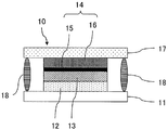
- FIG. 1 is a schematic cross-sectional view showing an example of an organic light emitting device manufactured by the method for manufacturing an organic light emitting device of the present invention.
- the stacking direction from the first substrate 11 toward the second substrate 17 is referred to as “up”.
- the organic light-emitting element 10 includes an anode 12 for injecting holes, an organic compound layer 13 including at least a light-emitting layer, and electrons are injected into the organic compound layer 13 on the first substrate 11.
- a cathode 14 for reflecting the emitted light toward the first substrate 11 is sequentially stacked.
- the cathode 14 includes an Al thin layer 15 formed so as to be adjacent to the organic compound layer 13 and a metal layer 16, and the metal layer 16 is opposite to the surface of the Al thin layer 15 adjacent to the organic compound layer 13. It is formed by being laminated so as to be adjacent to the surface.
- the first substrate 11 and the second substrate 17 are fixed by an adhesive member 18 sandwiched therebetween.
- the first substrate 11, together with the second substrate 17, serves as a support for forming the organic light emitting element 10 having the anode 12, the organic compound layer 13, and the cathode 14.
- the first substrate 11 In order to emit light from the first substrate 11 side in the organic light emitting device 10, the first substrate 11 needs to be transparent to the light emitted from the light emitting layer.
- the material used for the transparent first substrate 11 include glasses such as sapphire glass, soda glass, and quartz glass; transparent resins such as acrylic resin, polycarbonate resin, polyester resin, and silicone resin. Metal nitrides such as aluminum nitride; transparent metal oxides such as alumina.
- the resin film etc. which consist of the said transparent resin as the 1st board
- the material used for the second substrate 17 is not limited to one that is transparent to visible light, but is opaque. Can also be used. Specifically, in addition to the above transparent material, silicon (Si), copper (Cu), silver (Ag), gold (Au), platinum (Pt), tungsten (W), titanium (Ti), tantalum ( Ta) or niobium (Nb) alone, alloys thereof, or stainless steel can also be used.
- silicon (Si), copper (Cu), silver (Ag), gold (Au), platinum (Pt), tungsten (W), titanium (Ti), tantalum ( Ta) or niobium (Nb) alone, alloys thereof, or stainless steel can also be used.
- an insulating layer may be formed between the cathode 14 and the second substrate 17 to insulate them.
- the thicknesses of the first substrate 11 and the second substrate 17 are preferably 0.1 to 10 mm, more preferably 0.25 to 2 mm, although depending on the required mechanical strength.
- the anode 12 injects holes into the organic compound layer 13 by applying a voltage between the anode 14 and the anode 14.
- the material used for the anode 12 must have electrical conductivity, and the sheet resistance is preferably 1000 ⁇ / ⁇ or less, and 100 ⁇ / ⁇ or less in the temperature range of ⁇ 5 to 80 ° C. More preferably.
- ⁇ Conductive metal oxides, metals, and alloys can be used as materials that satisfy these conditions.
- the conductive metal oxide include ITO (indium tin oxide), IZO (indium zinc oxide), zinc oxide, and tin oxide.
- the metal include copper (Cu), silver (Ag), gold (Au), platinum (Pt), tungsten (W), titanium (Ti), tantalum (Ta), niobium (Nb), and the like.
- An alloy containing these metals and stainless steel can also be used.
- materials used for the transparent anode include indium oxide, zinc oxide, tin oxide, ITO (indium tin oxide) and IZO (indium zinc oxide) which are composites thereof, gold, platinum, silver, copper Is mentioned.
- ITO, IZO, and tin oxide are preferable in terms of high electrical conductivity and easy hole injection into the organic compound layer 13.
- a transparent conductive film made of an organic material such as polyaniline or a derivative thereof, polythiophene or a derivative thereof may be used.
- the thickness of the anode 12 is 2 to 300 nm in order to obtain high light transmissivity when light incident from the light emitting layer is to be emitted from the first substrate 11 side of the organic light emitting element 10 through the anode 12. Preferably there is.
- the thickness of the anode 12 is For example, it can be formed with a thickness of 2 nm to 2 mm.
- a vacuum deposition method such as a vacuum deposition method (resistance heating deposition method, induction heating deposition method, electron beam deposition method, etc.), sputtering method, ion plating method, CVD method or the like is used.
- Coating film forming methods such as a film method, a spin coating method, a dip coating method, an ink jet method, a printing method (such as a screen printing method), a spray method, and a dispenser method can be used.
- the organic compound layer 13 includes at least one organic compound layer including a light emitting layer or a plurality of stacked organic compound layers, and the light emitting layer emits light by applying a voltage between the anode 12 and the cathode 14. including.
- a light-emitting material a known light-emitting material can be used, and any of a light-emitting polymer compound and a light-emitting non-polymer compound can be used.
- cyclometalated complexes examples include 2-phenylpyridine derivatives, 7,8-benzoquinoline derivatives, 2- (2-thienyl) pyridine derivatives, 2- (1-naphthyl) pyridine derivatives, 2-phenylquinoline derivatives, and the like.
- the complex examples include iridium, platinum, and gold having a ligand, and an iridium complex is particularly preferable.
- the cyclometalated complex may have other ligands in addition to the ligands necessary for forming the cyclometalated complex.
- Examples of the light-emitting polymer compound include poly-p-phenylene vinylene (PPV) derivatives such as MEH-PPV (poly [2-methoxy-5- (2-ethylhexyloxy) -1,4-phenylene vinylene]), poly Examples include ⁇ -conjugated polymer compounds such as fluorene derivatives and polythiophene derivatives; polymers in which a dye molecule and a tetraphenyldiamine derivative or triphenylamine derivative are introduced into the main chain or side chain.
- a light emitting polymer compound and a light emitting non-polymer compound may be used in combination.
- the light emitting layer may contain a host material together with the light emitting material, and the light emitting material may be dispersed in the host material.
- a host material preferably has a charge transporting property, and is preferably a hole transporting compound or an electron transporting compound.
- the thickness of the light emitting layer is preferably 1 to 500 nm, more preferably 5 to 250 nm, and particularly preferably 10 to 100 nm.
- the organic compound layer 13 may include a hole transport layer for receiving holes from the anode 12 and transporting them to the light emitting layer between the anode 12 and the light emitting layer.
- a hole transport layer for receiving holes from the anode 12 and transporting them to the light emitting layer between the anode 12 and the light emitting layer.
- a known hole transport material can be used as a material for forming such a hole transport layer.
- TPD N, N′-diphenyl-N, N′-di (3-methylphenyl)) -1,1′-biphenyl-4,4′-diamine
- ⁇ -NPD 4,4′-bis [N- (1-naphthyl) -N-phenylamino] biphenyl
- m-MTDATA 4, 4 Triphenylamine derivatives such as', 4 ''-tris [N- (3-methylphenyl) -N-phenylamino] triphenylamine); polyvinylcarbazole; and introducing a polymerizable substituent into the triphenylamine derivative.
- Polymerized polymer compounds and the like can be mentioned.
- the above hole transport materials may be used singly or in combination of two or more, and a plurality of hole transport layers formed from different hole transport materials may be laminated.
- the thickness of the hole transport layer depends on the conductivity of the hole transport layer and cannot be generally limited, but is preferably 1 nm to 1 ⁇ m, more preferably 5 to 500 nm, and particularly preferably 10 to 100 nm.
- a hole injection layer having a thickness of 1 to 50 nm may be provided between the hole transport layer and the anode 12 in order to relax a hole injection barrier from the anode 12 to the hole transport layer.
- known materials such as copper phthalocyanine, a mixture of polyethylenedioxythiophene (PEDOT) and polystyrene sulfonic acid (PSS) (PEDOT: PSS), fluorocarbon, silicon dioxide, and the like are used.
- PES polystyrene sulfonic acid
- F4TCNQ 2,3,5,6-tetrafluorotetracyano-1,4-benzoquinodimethane
- the organic compound layer 13 may have an electron transport layer for receiving electrons from the cathode 14 and transporting them to the light emitting layer, between the light emitting layer and the cathode 14.
- Materials that can be used for such an electron transport layer include quinoline derivatives, phenanthroline derivatives, oxadiazole derivatives, perylene derivatives, pyridine derivatives, pyrimidine derivatives, quinoxaline derivatives, diphenylquinone derivatives, nitro-substituted fluorene derivatives, triarylboranes.
- electron transport materials such as derivatives, triazine derivatives, and triarylphosphine oxide derivatives.
- tris (8-quinolinolato) aluminum abbreviation: Alq
- bis [2- (2-hydroxyphenyl) benzoxazolate] zinc bis [2- (2-hydroxyphenyl) benzothiazolate] zinc
- 2- (4-biphenylyl) -5- (4-tert-butylphenyl) -1,3,4-oxadiazole More specifically, tris (8-quinolinolato) aluminum (abbreviation: Alq), bis [2- (2-hydroxyphenyl) benzoxazolate] zinc, bis [2- (2-hydroxyphenyl) benzothiazolate] zinc, And 2- (4-biphenylyl) -5- (4-tert-butylphenyl) -1,3,4-oxadiazole.
- the electron transport layer is preferably an electron transport layer containing an alkali metal or an alkali metal compound, and a mixture of the above electron transport material and an alkali metal having a small work function, or an alkali metal salt of the above electron transport material ( More preferably, it consists of an alkali metal compound.
- Such an electron transport layer has a high electron mobility and can drive the organic light emitting device 10 at a low voltage. However, by forming the Al thin layer 15 in contact with the electron transport layer, an electron injection barrier is increased. Can be reduced.
- the thickness of the electron transport layer depends on the conductivity of the electron transport layer and cannot be generally limited, but is preferably 1 to 500 nm, more preferably 5 to 100 nm.
- a thickness of 1 to 50 nm is provided between the electron transport layer and the light emitting layer.
- the hole blocking layer may be provided. This hole blocking layer can also be regarded as one of the layers included in the organic compound layer 13.
- a known material such as a triazole derivative, an oxadiazole derivative, or a phenanthroline derivative can be used.
- a cathode buffer layer may be provided on the organic compound layer 13 side adjacent to the cathode 14 for the purpose of lowering the electron injection barrier from the cathode 14 to the organic compound layer 13 and increasing the electron injection efficiency.
- a metal material having a work function lower than that of the cathode 14 is preferable.
- alkali metals Na, K, Rb, Cs
- alkaline earth metals Sr, Ba, Ca, Mg
- rare earth metals Pr, Sm, Eu, Yb
- fluorides or chlorides of these metals A material selected from oxides or a mixture of two or more can be used.
- the thickness of the cathode buffer layer is preferably from 0.1 to 50 nm, more preferably from 0.1 to 20 nm, and even more preferably from 0.5 to 10 nm.
- a cathode buffer layer made of an inorganic compound is regarded as one of the layers constituting the organic compound layer 13 for convenience.
- the same method as that for the anode 12 can be used to form the organic compound layer 13.
- the resistance heating vapor deposition method or the coating film forming method is more preferable for forming each layer included in the organic compound layer 13, and the coating film forming method is particularly preferable for forming the layer containing the polymer organic compound.
- a coating film forming method a coating liquid in which a material constituting a layer to be formed is dissolved or dispersed in a predetermined solvent such as an organic solvent or water is applied. After coating, a desired layer is formed by drying the coating solution by heating or vacuuming.
- the cathode 14 is a property of reflecting light emitted from the light emitting layer, that is, a light reflecting cathode.
- the cathode 14 preferably has a reflectance of 50 to 100% with respect to light emitted from the light emitting layer, and more preferably 70 to 100% or more.
- the step of forming the light-reflective cathode 14 includes (i) forming an Al thin layer 15 having a thickness of 0.1 nm to 10 nm adjacent to the organic compound layer 13. And (ii) a metal layer in which a metal layer 16 having a thickness of 70 nm to 10 ⁇ m is laminated adjacent to the surface of the Al thin layer 15 opposite to the surface adjacent to the organic compound layer 13. Laminating step.
- the Al thin layer forming step is performed in a vacuum of 1 ⁇ 10 ⁇ 8 to 1 ⁇ 10 ⁇ 2 Pa, and the Al thin layer obtained in the Al thin layer forming step is In the metal layer stacking step, a vacuum of 1 ⁇ 10 ⁇ 8 to 1 ⁇ 10 ⁇ 2 Pa is maintained until a metal layer is stacked adjacent to the Al thin layer. That is, the Al thin layer is maintained in a vacuum of 1 ⁇ 10 ⁇ 8 to 1 ⁇ 10 ⁇ 2 Pa during the formation and after the Al thin layer is formed until the metal layer is laminated. .
- the Al thin layer forming step and the metal layer laminating step are performed in a vacuum of 1 ⁇ 10 ⁇ 8 to 1 ⁇ 10 ⁇ 2 Pa, and the Al thin layer forming step and the metal layer laminating step are When another process is included in between, the process is performed in a vacuum of 1 ⁇ 10 ⁇ 8 to 1 ⁇ 10 ⁇ 2 Pa including this process.
- a process of inspecting an Al thin layer between the Al thin layer forming process and the metal layer laminating process a transporting process of the substrate on which the Al thin layer is formed, and the like. It is done.
- the Al thin layer 15 is an active layer that injects electrons into the organic compound layer 13.
- the Al thin layer 15 is formed using a vacuum film formation method, and specifically, a vacuum evaporation method (resistance heating evaporation method, induction heating evaporation method, electron beam evaporation method, etc.), sputtering method, ion plating method.
- the film is formed by a method such as the CVD method, and the film formation by a vacuum evaporation method is particularly preferable because it is easy to form a large area with a uniform film thickness.
- the Al thin layer 15 is a thin layer having a thickness of 0.1 to 10 nm, the time during which the organic compound layer 13 is exposed to a high temperature can be shortened, and while maintaining the characteristics of efficient electron injection of Al, Damage to the compound layer can be suppressed.
- the Al thin layer having the above thickness has optical transparency.
- the thickness of the Al thin layer 15 is more preferably 0.1 to 5 nm.
- the film thickness of the Al thin layer 15 is in the above range.
- the metal layer 16 which is one of the layers constituting the cathode 14, is a layer for supplementing the light reflectivity and electrical conductivity of the Al thin layer 15, and includes a surface adjacent to the organic compound layer 13 of the Al thin layer 15. Are formed adjacent to the opposite surface.
- the material used for the metal layer 16 is not particularly limited as long as it has light reflectivity and electrical conductivity, and a single metal or an alloy is desirable. Among simple metals, Ag, Al, and Rh having high light reflectivity over the entire visible light region are preferable.
- the thickness of the metal layer 16 is preferably 70 nm to 10 ⁇ m, more preferably 100 nm to 1 ⁇ m, from the viewpoint of easy formation and high light reflectivity and electrical conductivity.
- the metal layer 16 is formed on the Al thin layer 15 while keeping the vacuum after the Al thin layer 15 is formed in a vacuum of 1 ⁇ 10 ⁇ 8 to 1 ⁇ 10 ⁇ 2 Pa. Accordingly, the cathode 14 can be formed while maintaining high Al activity at the interface between the Al thin layer 15 and the organic compound layer 13.
- the metal layer 16 is directly deposited on the Al thin layer 15 in a vacuum, and the metal layer 16 is made of Al or requires higher energy for film formation than Al.
- a metal such as Rh
- the metal layer 16 is separately deposited on the second substrate 17, and the metal layer 16 is laminated together with the second substrate 17 so that the metal layer 16 overlaps the Al thin layer 15. Then, damage to the organic compound layer 13 when the metal layer 16 is laminated can be suppressed.
- a method for forming the metal layer 16 on the second substrate 17 the same method as that for the anode 12 can be used.
- the metal layer 16 is not necessarily formed on the second substrate 17 in a vacuum. After the film is formed by a coating method or the like under an atmospheric pressure, the film is formed in a vacuum (1 ⁇ 10 ⁇ 8 to 1 ⁇ 10 6). -2 Pa) may be bonded to the Al thin layer 15.
- the second substrate 17 is preferably bonded to the first substrate 11 by an adhesive member 18 such as a photo-curable resin or a thermosetting resin.
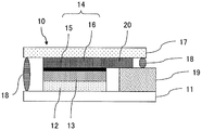
- FIG. 2 is a schematic cross-sectional view showing an example of an embodiment of an organic light emitting device manufactured by the method for manufacturing an organic light emitting device of the present invention, including a terminal portion and a wiring portion.
- the organic light emitting device 10 shown in FIG. 2 includes a terminal portion 19 for electrically connecting the cathode 14 to a power source and wiring for electrically connecting the terminal portion 19 to the cathode 14.
- Part 20 is also shown in the figure.
- the wiring part 20 is formed with the metal layer 16 on the same surface of the second substrate 17, and may be formed of any material as long as it has electrical conductivity.
- the wiring part 20 is formed integrally with the metal layer 16 by the same material as the metal layer 16. In other words, the wiring part 20 is made of the same metal as the metal layer 16 and is electrically connected to the metal layer.
- the wiring portion 20 is formed on the second substrate 17 at the same time as the metal layer 16, the wiring portion 20 is electrically connected to the terminal portion 19 when the metal layer 16 is closely attached to the Al thin layer 15.
- the manufacturing process of the organic light emitting device can be simplified as compared with the case where the wiring portion for electrically connecting the metal layer 16 and the terminal portion 19 is separately formed. It is possible to prevent the light emitting layer from being damaged by heat or the like.
- the thickness of the terminal portion 19 is the same as the total thickness of the anode 12, the organic compound layer 13, and the Al thin layer 15 so that the terminal portion 19 and the wiring portion 20 are in contact with each other. And / or by making the 2nd board
- the terminal portion 19 is provided in a region including at least a part of the outer edge portion on the first substrate 11 and acts to electrically connect the cathode 14 to a power source. Therefore, any material having conductivity may be used.
- a method for forming the terminal portion 19 can be the same as the method for forming the anode 12. However, when the anode 12 is formed on the substrate 11 using the same material as the anode 12 as the material for the terminal portion 19. Moreover, the manufacturing process of the organic light emitting device can be simplified by forming the terminal portion 19 together with the anode 12.
- the metal layer 16 may be formed by peeling the second metal layer 17 from the second substrate 17 after the metal layer 16 is brought into close contact with the Al thin layer 15.
- a metal foil or a polyimide sheet having an insulating film such as silicon oxide formed on the surface is used as the second substrate 17.
- the shape of the second substrate 17 may be flat or cylindrical.
- a peeling layer may be formed on the surface of the second substrate 17, and the metal layer 16 is formed in an arbitrary pattern by forming the peeling layer with a material that is softened by heating. You can also Note that the peeling step may be performed under atmospheric pressure.
- the protective layer is provided so as to cover the upper part and / or the side part of the organic light emitting device 10.
- a material for the protective layer a polymer compound, a metal oxide, a metal fluoride, a metal boride, or a silicon compound such as silicon nitride or silicon oxide can be used.
- these protective layers may be laminated
- the protective cover is provided without touching the organic light emitting element 10 so as to cover the upper part and / or the side part of the organic light emitting element 10.
- the protective cover a glass plate, a plastic plate whose surface is subjected to low water permeability treatment, a metal, or the like can be used.
- the protective cover is preferably bonded to the first substrate 11 with a thermosetting resin or a photocurable resin to seal at least the light emitting portion of the organic light emitting element 10.
- the second substrate 17 may also serve as the protective cover. It is preferable to seal an inert gas such as nitrogen, argon, or helium in the sealed space because it is easy to prevent the cathode 14 from being oxidized.
- FIG. 3 is a schematic cross-sectional view illustrating another example of an organic light emitting device manufactured by the method for manufacturing an organic light emitting device of the present invention.
- the organic light emitting element 30 has a structure in which an anode 32, an organic compound layer 33 including at least a light emitting layer, and a cathode 34 are sequentially stacked on a first substrate 31, and the cathode 34 is formed on the organic compound layer 33. It has the adjacent Al thin layer 35 and the metal layer 36 adjacent to the surface of the Al thin layer 35 opposite to the surface adjacent to the organic compound layer 33.
- the step of forming the cathode 34 includes (i) an Al thin layer forming step of forming an Al thin layer 35 having optical transparency adjacent to the organic compound layer 33, and (ii) an organic compound of the Al thin layer 35.
- the Al thin layer forming step is performed in a vacuum of 1 ⁇ 10 ⁇ 8 to 1 ⁇ 10 ⁇ 2 Pa, and the Al thin layer obtained in the Al thin layer forming step is performed.
- the metal layer 36 is directly formed on the Al thin layer 35 without being bonded after being once formed on a substrate different from the first substrate 31.
- the Al thin layer 35 in the organic light emitting device 30 performs efficient electron injection into the organic compound layer 33, so that 1 ⁇ 10 ⁇ 8 to 1 ⁇ It is formed in contact with the organic compound layer 33 in a vacuum of 10 ⁇ 2 Pa.
- the Al thin layer 35 is formed using a vacuum film formation method, and specifically, a vacuum evaporation method (resistance heating evaporation method, induction heating evaporation method, electron beam evaporation method, etc.), sputtering method, ion plating method, CVD.
- the film is formed by a method such as a method, and in particular, the film formation by a vacuum evaporation method is preferable because it is easy to form a large area with a uniform film thickness.
- the metal layer 36 is a layer for supplementing the light reflectivity and electrical conductivity of the Al thin layer 35. After the Al thin layer 35 is formed, the metal layer 36 is in a vacuum of 1 ⁇ 10 ⁇ 8 to 1 ⁇ 10 ⁇ 2 Pa. Is formed. As the material of the metal layer 36, a simple substance or an alloy of metal having light reflectivity and electrical conductivity and capable of forming a film at a temperature lower than that of Al is used.
- the metal layer 36 is preferably a metal layer made of at least one metal selected from the group consisting of Ag, Sb, In, Mg, Mn, Pb and Zn or an alloy thereof.
- the metal layer 36 a metal layer made of at least one metal selected from the group consisting of Ag and Pb having a high light reflectance over the entire visible light region or an alloy thereof is preferable, and a metal layer made of Ag is particularly preferable. preferable.
- the metal layer 36 is formed by a vacuum film forming method, but it is preferable to form the metal layer 36 by a vacuum vapor deposition method which can be formed at a relatively low temperature and can easily form a large area with a uniform film thickness. By forming the metal layer 36 in this manner, damage to the organic compound layer due to heat or the like can be suppressed while maintaining the characteristics of efficient electron injection of Al.
- the thickness of the metal layer 36 is preferably 70 nm to 10 ⁇ m, more preferably 100 nm to 1 ⁇ m from the viewpoint of easy formation and high light reflectivity and electrical conductivity.
- the organic light-emitting device manufactured by the method for manufacturing an organic light-emitting device of the present invention is suitably used for an image display device as a pixel by a matrix method or a segment method.
- the organic light emitting element is also suitably used as an illumination device such as a surface light source without forming pixels.
- the organic light-emitting device manufactured by the organic light-emitting device manufacturing method of the present invention includes a display device in a computer, a television, a mobile terminal, a mobile phone, a car navigation system, a sign, a signboard, a video camera viewfinder, It is suitably used for a light irradiation device in a backlight, electrophotography, illumination, resist exposure, reading device, interior illumination, optical communication system and the like.
- a phosphorescent polymer compound (A) represented by the following formula was synthesized according to the method described in the examples of WO2010 / 016512.
- solution A a light emitting material solution
- the organic light emitting device 10 shown in FIG. 2 was produced by the following method.
- a sputtering apparatus (E-401s manufactured by Canon Anelva Co., Ltd.) is used to form an anode 12 having a thickness of 150 nm by sputtering.
- the ITO thin film was patterned to correspond to a 20 mm square light emitting region, and at the same time, an ITO film having a thickness of 150 nm was formed as a terminal portion 19 on one side of the glass substrate.
- the solution A is applied onto the ITO anode 12 by a spin coating method (3000 rpm, 30 seconds), left to stand at 140 ° C. for 1 hour in a nitrogen atmosphere, and dried, whereby light emission as a part of the organic compound layer 13 is obtained.
- the layer was formed with a thickness of 80 nm.
- an Al layer of 5 nm was formed on the electron transport layer as the Al thin layer 15 in a vacuum of 2.1 ⁇ 10 ⁇ 4 Pa using a vacuum deposition apparatus.
- the second substrate 17 a 70 nm Ag layer was formed on a glass substrate (23 mm square, thickness 0.25 mm) made of quartz glass by using a vacuum evaporation apparatus.
- the Ag layer is formed on the Al layer and the ITO film as the terminal portion 19 while maintaining a vacuum of 2.1 ⁇ 10 ⁇ 4 Pa in a vacuum deposition apparatus.
- the first substrate 11 and the second substrate 17 were fixed using a photocurable resin so as to be in contact with each other, thereby forming an Ag layer as the metal layer 16.
- a voltage was applied to the produced organic light emitting device 10 using a constant voltage power supply ammeter (SM2400 manufactured by Keith Instruments Inc.), and the luminance intensity in the direction perpendicular to the first substrate 11 of the organic light emitting device 10 was measured. (Measured with BM-9 manufactured by Topcon Corporation). And when the luminous efficiency was determined from the ratio of the luminous intensity to the current density, the luminous efficiency was 35 cd / A. Further, when the light emitting surface was visually observed, the luminance distribution was uniform.
- SM2400 constant voltage power supply ammeter
- Example 2 The organic light emitting device 10 was produced in the same manner as in Example 1 except that a 120 nm Al layer was formed as the metal layer 16 instead of the 70 nm Ag layer.
- the produced organic light emitting device had a luminous efficiency of 37 cd / A, and the luminance distribution within the light emitting surface was visually uniform.
- the organic light emitting device 30 shown in FIG. 3 was produced by the following method.
- Example 1 a light emitting layer and an electron transport layer as an organic compound layer 33 and an Al layer as an Al thin layer 35 were formed on a glass substrate as a first substrate 31, respectively.
- a 100 nm Ag layer was formed by vacuum evaporation as the metal layer 36 while maintaining the vacuum of 2.1 ⁇ 10 ⁇ 4 Pa after the formation of the Al layer.
- the produced organic light emitting device 30 had a luminous efficiency of 33 cd / A, and the luminance distribution in the light emitting surface was visually uniform.
- Example 3 In Example 3, without forming the metal layer 36, the thickness of the Al layer as the Al thin layer 35 was changed from 5 nm to 100 nm, and the Al layer was used as a light-reflective cathode to produce an organic light emitting device. did. The average luminous efficiency in the light emitting surface of the produced organic light emitting device was 16 cd / A, and the luminance distribution in the light emitting surface was visually non-uniform.
Landscapes
- Engineering & Computer Science (AREA)
- Manufacturing & Machinery (AREA)
- Physics & Mathematics (AREA)
- Optics & Photonics (AREA)
- Electroluminescent Light Sources (AREA)
Abstract
Description
前記光反射性の陰極を形成する工程が、
(i)前記有機化合物層に隣接して、厚さが0.1~10nmのAl薄層を形成するAl薄層形成工程と、
(ii)前記Al薄層の、前記有機化合物層に隣接する面とは反対の面に隣接して、厚さが70nm~10μmの金属層を積層する金属層積層工程とを含み、
前記Al薄層形成工程を1×10⁻⁸~1×10⁻²Paの真空中で行い、前記Al薄層形成工程で得られたAl薄層を、前記金属層積層工程により該Al薄層に隣接して金属層が積層されるまで、1×10⁻⁸~1×10⁻²Paの真空中に保持する、有機発光素子の製造方法。
前記金属層が、Ag、Sb、In、Mg、Mn、PbおよびZnからなる群より選択される少なくとも1種の金属またはその合金からなり、
前記金属層積層工程が、前記Al薄層の表面に真空蒸着法により前記金属層を形成する工程である、(1)に記載の有機発光素子の製造方法。
前記第2の基板が、前記金属層と同一の面上に、前記金属層と同じ金属からなり、前記金属層に電気的に接続した配線部を有し、
前記金属層積層工程において、前記端子部と前記配線部とを電気的に接続する、(3)または(4)に記載の有機発光素子の製造方法。
WO2010/016512号公報の実施例に記載された方法に従って下記式で表される燐光発光性高分子化合物(A)を合成した。高分子化合物(A)の重量平均分子量は52,000、各繰り返し単位のモル比はk:m:n=6:42:52であった。

有機発光素子として、図2に示した有機発光素子10を、以下の方法により作製した。
金属層16として、70nmのAg層に替えて120nmのAl層を形成したほかは、実施例1と同様にして有機発光素子10を作製した。作製した有機発光素子の発光効率は37cd/Aであり、発光面内の輝度の分布は、目視で均一であった。
有機発光素子として、図3に示した有機発光素子30を、以下の方法により作製した。
実施例3において、金属層36を形成せずに、Al薄層35としてのAl層の厚さを5nmから100nmに変更し、Al層を光反射性の陰極とすることで有機発光素子を作製した。作製した有機発光素子の発光面内の平均発光効率は16cd/Aであり、発光面内の輝度の分布は、目視で不均一であった。
11・・・第1の基板
12・・・陽極
13・・・有機化合物層
14・・・陰極
15・・・Al薄層
16・・・金属層
17・・・第2の基板
18・・・接着部材
19・・・端子部
20・・・配線部
30・・・有機発光素子
31・・・第1の基板
32・・・陽極
33・・・有機化合物層
34・・・陰極
35・・・Al薄層
36・・・金属層
Claims (7)
- 第1の基板、陽極、少なくとも発光層を含む有機化合物層、および光反射性の陰極がこの順で積層された有機発光素子の製造方法であって、
前記光反射性の陰極を形成する工程が、
(i)前記有機化合物層に隣接して、厚さが0.1~10nmのAl薄層を形成するAl薄層形成工程と、
(ii)前記Al薄層の、前記有機化合物層に隣接する面とは反対の面に隣接して、厚さが70nm~10μmの金属層を積層する金属層積層工程とを含み、
前記Al薄層形成工程を1×10⁻⁸~1×10⁻²Paの真空中で行い、前記Al薄層形成工程で得られたAl薄層を、前記金属層積層工程により該Al薄層に隣接して金属層が積層されるまで、1×10⁻⁸~1×10⁻²Paの真空中に保持する、有機発光素子の製造方法。 - 前記Al薄層形成工程が、前記有機化合物層の表面に真空蒸着法により前記Al薄層を形成する工程であり、
前記金属層が、Ag、Sb、In、Mg、Mn、PbおよびZnからなる群より選択される少なくとも1種の金属またはその合金からなり、
前記金属層積層工程が、前記Al薄層の表面に真空蒸着法により前記金属層を形成する工程である、請求項1に記載の有機発光素子の製造方法。 - 前記金属層積層工程が、第2の基板上に形成された厚さが70nm~10μmの金属層を、前記第2の基板とともに前記Al薄層に密着させることで積層する工程である、請求項1に記載の有機発光素子の製造方法。
- 前記金属層が、Ag、AlおよびRhからなる群より選択される少なくとも1種の金属または合金からなる、請求項3に記載の有機発光素子の製造方法。
- 前記陰極を形成する工程が、前記金属層積層工程の後に、前記金属層を前記第2の基板から剥離する工程を含む、請求項3または4に記載の有機発光素子の製造方法。
- 前記有機発光素子が、前記第1の基板上の少なくとも外縁部の一部を含む領域に、前記陰極を電源に電気接続するための端子部を有し、
前記第2の基板が、前記金属層と同一の面上に、前記金属層と同じ金属からなり、前記金属層に電気的に接続した配線部を有し、
前記金属層積層工程において、前記端子部と前記配線部とを電気的に接続する、請求項3または4に記載の有機発光素子の製造方法。 - 前記有機化合物層が、前記Al薄層に隣接したアルカリ金属またはアルカリ金属化合物を含む電子輸送層を有する、請求項1~6のいずれか一項に記載の有機発光素子の製造方法。
Priority Applications (2)
| Application Number | Priority Date | Filing Date | Title |
|---|---|---|---|
| CN201280060966.3A CN103988581A (zh) | 2011-12-21 | 2012-11-28 | 有机发光元件的制造方法 |
| US14/367,100 US20140363909A1 (en) | 2011-12-21 | 2012-11-28 | Method of producing an organic light emitting element |
Applications Claiming Priority (2)
| Application Number | Priority Date | Filing Date | Title |
|---|---|---|---|
| JP2011-279898 | 2011-12-21 | ||
| JP2011279898 | 2011-12-21 |
Publications (1)
| Publication Number | Publication Date |
|---|---|
| WO2013094375A1 true WO2013094375A1 (ja) | 2013-06-27 |
Family
ID=48668274
Family Applications (1)
| Application Number | Title | Priority Date | Filing Date |
|---|---|---|---|
| PCT/JP2012/080693 Ceased WO2013094375A1 (ja) | 2011-12-21 | 2012-11-28 | 有機発光素子の製造方法 |
Country Status (4)
| Country | Link |
|---|---|
| US (1) | US20140363909A1 (ja) |
| JP (1) | JPWO2013094375A1 (ja) |
| CN (1) | CN103988581A (ja) |
| WO (1) | WO2013094375A1 (ja) |
Cited By (2)
| Publication number | Priority date | Publication date | Assignee | Title |
|---|---|---|---|---|
| WO2015059197A1 (de) * | 2013-10-24 | 2015-04-30 | Osram Oled Gmbh | Optoelektronisches bauelement, optoelektronische baugruppe, verfahren zum herstellen eines optoelektronischen bauelements und verfahren zum herstellen einer optoelektronischen baugruppe |
| JP2017212042A (ja) * | 2016-05-23 | 2017-11-30 | 株式会社カネカ | 有機el素子 |
Citations (6)
| Publication number | Priority date | Publication date | Assignee | Title |
|---|---|---|---|---|
| JPH10270172A (ja) * | 1997-01-27 | 1998-10-09 | Junji Kido | 有機エレクトロルミネッセント素子 |
| JPH10335060A (ja) * | 1997-06-03 | 1998-12-18 | Sony Corp | 有機電界発光素子 |
| JPH1126167A (ja) * | 1997-04-04 | 1999-01-29 | Mitsubishi Chem Corp | 有機電界発光素子 |
| JPH11329743A (ja) * | 1998-05-19 | 1999-11-30 | Stanley Electric Co Ltd | 電界発光素子およびその製造方法 |
| JP2002237382A (ja) * | 2001-02-13 | 2002-08-23 | Stanley Electric Co Ltd | 有機led素子及びその製造方法 |
| JP2010015998A (ja) * | 2009-09-07 | 2010-01-21 | Semiconductor Energy Lab Co Ltd | 表示装置 |
Family Cites Families (4)
| Publication number | Priority date | Publication date | Assignee | Title |
|---|---|---|---|---|
| JPH10270171A (ja) * | 1997-01-27 | 1998-10-09 | Junji Kido | 有機エレクトロルミネッセント素子 |
| US6121727A (en) * | 1997-04-04 | 2000-09-19 | Mitsubishi Chemical Corporation | Organic electroluminescent device |
| US6893743B2 (en) * | 2000-10-04 | 2005-05-17 | Mitsubishi Chemical Corporation | Organic electroluminescent device |
| US20080057183A1 (en) * | 2006-08-31 | 2008-03-06 | Spindler Jeffrey P | Method for lithium deposition in oled device |
-
2012
- 2012-11-28 JP JP2013550197A patent/JPWO2013094375A1/ja active Pending
- 2012-11-28 WO PCT/JP2012/080693 patent/WO2013094375A1/ja not_active Ceased
- 2012-11-28 CN CN201280060966.3A patent/CN103988581A/zh active Pending
- 2012-11-28 US US14/367,100 patent/US20140363909A1/en not_active Abandoned
Patent Citations (6)
| Publication number | Priority date | Publication date | Assignee | Title |
|---|---|---|---|---|
| JPH10270172A (ja) * | 1997-01-27 | 1998-10-09 | Junji Kido | 有機エレクトロルミネッセント素子 |
| JPH1126167A (ja) * | 1997-04-04 | 1999-01-29 | Mitsubishi Chem Corp | 有機電界発光素子 |
| JPH10335060A (ja) * | 1997-06-03 | 1998-12-18 | Sony Corp | 有機電界発光素子 |
| JPH11329743A (ja) * | 1998-05-19 | 1999-11-30 | Stanley Electric Co Ltd | 電界発光素子およびその製造方法 |
| JP2002237382A (ja) * | 2001-02-13 | 2002-08-23 | Stanley Electric Co Ltd | 有機led素子及びその製造方法 |
| JP2010015998A (ja) * | 2009-09-07 | 2010-01-21 | Semiconductor Energy Lab Co Ltd | 表示装置 |
Cited By (2)
| Publication number | Priority date | Publication date | Assignee | Title |
|---|---|---|---|---|
| WO2015059197A1 (de) * | 2013-10-24 | 2015-04-30 | Osram Oled Gmbh | Optoelektronisches bauelement, optoelektronische baugruppe, verfahren zum herstellen eines optoelektronischen bauelements und verfahren zum herstellen einer optoelektronischen baugruppe |
| JP2017212042A (ja) * | 2016-05-23 | 2017-11-30 | 株式会社カネカ | 有機el素子 |
Also Published As
| Publication number | Publication date |
|---|---|
| CN103988581A (zh) | 2014-08-13 |
| US20140363909A1 (en) | 2014-12-11 |
| JPWO2013094375A1 (ja) | 2015-04-27 |
Similar Documents
| Publication | Publication Date | Title |
|---|---|---|
| US8507314B2 (en) | Organic light emitting device and manufacturing method thereof | |
| TW200524470A (en) | Organic electroluminescent element and organic electroluminescent device including the same | |
| WO2011040294A1 (ja) | 有機エレクトロルミネッセンス素子 | |
| JP2003045643A (ja) | 発光素子、および表示装置 | |
| CN102598865A (zh) | 有机电致发光元件和包括有机电致发光元件的显示器 | |
| JP5312949B2 (ja) | 電気活性デバイス用積層電極及びその製造方法 | |
| WO2011040501A1 (ja) | 有機el装置 | |
| JP2003123990A (ja) | 有機エレクトロルミネッセンス素子 | |
| WO2013146350A1 (ja) | 発光装置および発光装置の製造方法 | |
| JPWO2017056682A1 (ja) | 有機エレクトロルミネッセンスパネル | |
| JPWO2017056684A1 (ja) | 有機エレクトロルミネッセンスパネル及びその製造方法 | |
| JP2006253055A (ja) | 有機エレクトロルミネッセンス素子用フレキシブル基板及びそれを用いた有機エレクトロルミネッセンス素子 | |
| TW200527713A (en) | Light-emitting device with increased quantum efficiency | |
| JP2010153091A (ja) | 有機エレクトロルミネッセンス素子 | |
| WO2013094375A1 (ja) | 有機発光素子の製造方法 | |
| JP5960047B2 (ja) | 有機エレクトロルミネッセンス素子及びその製造方法 | |
| US20140048793A1 (en) | Organic light-emitting element, production method for organic light-emitting element, display device, and illumination device | |
| JP2015090817A (ja) | 有機発光素子、有機発光素子の製造方法、表示装置および照明装置 | |
| JP2008235193A (ja) | 有機電界発光素子 | |
| JP2012243517A (ja) | 有機発光素子、有機発光素子の製造方法、表示装置および照明装置 | |
| US20140203255A1 (en) | Organic light-emitting element, method for manufacturing organic light-emitting element, display device and illumination device | |
| Hao et al. | Top emitting poly (p-phenylene vinylene) light-emitting diodes on metal sandwiched polyethylene terephthalate substrates | |
| JP2006286238A (ja) | フレキシブル有機el素子とその製造方法 | |
| US20140084278A1 (en) | Organic light-emitting element, method for making organic light-emitting element, display device and illumination device | |
| JPWO2016072246A1 (ja) | 有機エレクトロルミネッセンス素子 |
Legal Events
| Date | Code | Title | Description |
|---|---|---|---|
| 121 | Ep: the epo has been informed by wipo that ep was designated in this application |
Ref document number: 12860628 Country of ref document: EP Kind code of ref document: A1 |
|
| ENP | Entry into the national phase |
Ref document number: 2013550197 Country of ref document: JP Kind code of ref document: A |
|
| WWE | Wipo information: entry into national phase |
Ref document number: 14367100 Country of ref document: US |
|
| NENP | Non-entry into the national phase |
Ref country code: DE |
|
| 122 | Ep: pct application non-entry in european phase |
Ref document number: 12860628 Country of ref document: EP Kind code of ref document: A1 |