WO2013094099A1 - 放射線検出器およびその製造方法 - Google Patents
放射線検出器およびその製造方法 Download PDFInfo
- Publication number
- WO2013094099A1 WO2013094099A1 PCT/JP2012/006751 JP2012006751W WO2013094099A1 WO 2013094099 A1 WO2013094099 A1 WO 2013094099A1 JP 2012006751 W JP2012006751 W JP 2012006751W WO 2013094099 A1 WO2013094099 A1 WO 2013094099A1
- Authority
- WO
- WIPO (PCT)
- Prior art keywords
- polycrystalline film
- semiconductor
- support substrate
- region
- radiation detector
- Prior art date
- Legal status (The legal status is an assumption and is not a legal conclusion. Google has not performed a legal analysis and makes no representation as to the accuracy of the status listed.)
- Ceased
Links
Images

Classifications
-
- G—PHYSICS
- G01—MEASURING; TESTING
- G01T—MEASUREMENT OF NUCLEAR OR X-RADIATION
- G01T1/00—Measuring X-radiation, gamma radiation, corpuscular radiation, or cosmic radiation
- G01T1/16—Measuring radiation intensity
- G01T1/24—Measuring radiation intensity with semiconductor detectors
-
- H—ELECTRICITY
- H10—SEMICONDUCTOR DEVICES; ELECTRIC SOLID-STATE DEVICES NOT OTHERWISE PROVIDED FOR
- H10F—INORGANIC SEMICONDUCTOR DEVICES SENSITIVE TO INFRARED RADIATION, LIGHT, ELECTROMAGNETIC RADIATION OF SHORTER WAVELENGTH OR CORPUSCULAR RADIATION
- H10F30/00—Individual radiation-sensitive semiconductor devices in which radiation controls the flow of current through the devices, e.g. photodetectors
- H10F30/20—Individual radiation-sensitive semiconductor devices in which radiation controls the flow of current through the devices, e.g. photodetectors the devices having potential barriers, e.g. phototransistors
- H10F30/29—Individual radiation-sensitive semiconductor devices in which radiation controls the flow of current through the devices, e.g. photodetectors the devices having potential barriers, e.g. phototransistors the devices being sensitive to radiation having very short wavelengths, e.g. X-rays, gamma-rays or corpuscular radiation
-
- H—ELECTRICITY
- H10—SEMICONDUCTOR DEVICES; ELECTRIC SOLID-STATE DEVICES NOT OTHERWISE PROVIDED FOR
- H10F—INORGANIC SEMICONDUCTOR DEVICES SENSITIVE TO INFRARED RADIATION, LIGHT, ELECTROMAGNETIC RADIATION OF SHORTER WAVELENGTH OR CORPUSCULAR RADIATION
- H10F39/00—Integrated devices, or assemblies of multiple devices, comprising at least one element covered by group H10F30/00, e.g. radiation detectors comprising photodiode arrays
- H10F39/10—Integrated devices
- H10F39/12—Image sensors
- H10F39/18—Complementary metal-oxide-semiconductor [CMOS] image sensors; Photodiode array image sensors
- H10F39/189—X-ray, gamma-ray or corpuscular radiation imagers
- H10F39/1892—Direct radiation image sensors
Definitions
- the present invention relates to a radiation detector having a function of detecting radiation including X-rays, ⁇ -rays, light, etc., and used for industrial purposes such as medical and foreign matter inspection, and a method for manufacturing the same.
- CdTe cadmium telluride
- CdZnTe zinc cadmium telluride
- the polycrystalline film of CdTe or CdZnTe is formed by proximity sublimation (for example, Patent Documents 1 and 2).
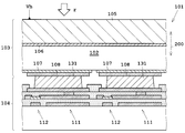
- a conventional radiation detector 101 is shown in FIG.
- the symbol r in FIG. 6 indicates the incident direction of radiation.
- the counter substrate (also referred to as a detection substrate) 103 is, in order from the radiation incident side, a conductive graphite support substrate 105 that functions as a common electrode to which a bias voltage Vh is applied, an electron injection blocking layer 106, and radiation.
- Each layer (film) of a semiconductor layer (radiation conversion layer) 102 that generates charges, a hole injection blocking layer 107, and a counter electrode 108 is laminated.
- the counter substrate 103 is integrally formed by being bonded to the active matrix substrate 104 via the bump electrodes 131.
- the active matrix substrate 104 has a capacitor 111 and a switching element 112 for each pixel, accumulates charges generated in the semiconductor layer 102 in accordance with incident radiation intensity, and reads the accumulated charges.
- Patent Document 1 when a polycrystalline semiconductor layer 102, that is, a semiconductor polycrystalline film 102 is formed, a large grain size polycrystalline region having a large grain size is formed by increasing the deposition temperature. First, a high temperature film forming process for forming a layer on the electron injection blocking layer 106) is performed first, and then a low temperature film forming process for forming a small grain polycrystalline film having a small particle size by lowering the film forming temperature is performed. It is disclosed. Further, in Patent Document 2, a source containing Cl is used to dope Cl at the time of forming the detection layer (semiconductor polycrystalline film) 102 to uniformize crystal grains, and further after the detection layer 102 is formed. It is disclosed to uniformly dope Cl by doping Cl.
- the detection characteristics of the semiconductor polycrystalline film 102 of the radiation detector 101 vary greatly depending on the film quality, particularly the crystal structure of the film (distribution in the thickness direction 200 of the crystal grains). Specifically, when the crystal grain size is large, the sensitivity is improved, but the variation between the pixels becomes large, and the leak current also depends on the presence or absence of a crystal grain boundary (crystal grain) that runs vertically in the thickness direction 200 of the semiconductor polycrystalline film. The variation between them becomes very large.
- the semiconductor polycrystalline film 102 includes a crystal grain (hereinafter referred to as “through grain” as appropriate) having a longitudinal direction in the thickness direction 200 of the semiconductor polycrystalline film 102 (reference numeral 201). It is assumed that the case where there are a plurality of crystal grains in the thickness direction 200 of the semiconductor polycrystalline film 102 (reference numeral 202) is mixed. Since the crystal grain boundary serves as a path for leakage current in the semiconductor polycrystalline film 102, the generated grains and the leakage current are more likely to flow through the through grains 201 than the plurality of crystal grains 202.
- the present invention has been made in view of such circumstances, and an object of the present invention is to provide a radiation detector capable of reducing variation between pixels due to leakage current and a method for manufacturing the same.
- the inventor has earnestly studied to solve the above problems, and as a result, has obtained the following knowledge.
- the crystal grain size grows large at the beginning, the crystal grain grows to the same diameter or larger than that, so that the penetrating grains 201 that run vertically in the thickness direction 200 of the semiconductor polycrystalline film are likely to be formed. For this reason, it is necessary to first form small crystal grains in the semiconductor polycrystalline film.
- the radiation detector manufacturing method includes a semiconductor polycrystalline film that generates charges in response to radiation, a support substrate provided on one surface of the semiconductor polycrystalline film, and the semiconductor polycrystalline film.
- a manufacturing method of a radiation detector comprising individual electrodes provided in a matrix for each pixel on the opposite side of the support substrate across the film, the crystal grain size of the semiconductor polycrystalline film from the individual electrode side And a step of forming the semiconductor polycrystalline film on the support substrate so as to be smaller on the support substrate side.
- the crystal grain size of the semiconductor polycrystalline film is smaller on the support substrate side than on the individual electrode side. Since the crystal grain size on the support substrate side formed earlier is small, it is possible to prevent the formation of through grains in which the crystal grain boundaries run vertically in the thickness direction of the semiconductor polycrystalline film, and the sensitivity and leakage current of the semiconductor polycrystalline film Can be reduced. As a result, it is possible to obtain a radiation image with uniform sensitivity and leak current of each pixel, low pixel noise, and excellent diagnostic visibility.
- the crystal grain size of the semiconductor polycrystalline film is formed to be smaller than the pixel pitch on the individual electrode side. Therefore, the dispersion
- an example of the semiconductor polycrystalline film is composed of CdTe or CdZnTe.
- An example of the method of manufacturing a radiation detector according to the present invention includes the step of forming the semiconductor polycrystalline film, the step of forming a first polycrystalline film region on the support substrate, and the first polycrystalline film region. And forming a second polycrystalline film region on the first polycrystalline film region while doping a predetermined amount of Cl, and the second polycrystalline film region is formed by doping the first polycrystalline film region. That is, the amount of Cl to be doped is smaller than that of one polycrystalline film region or is formed without doping with Cl. Thereby, the crystal grain of the 1st polycrystalline film area by the side of a support substrate can be made smaller than the 2nd polycrystalline film area by the side of an individual electrode.
- An example of the method of manufacturing a radiation detector according to the present invention includes the step of forming the semiconductor polycrystalline film, the step of forming a first polycrystalline film region on the support substrate, and the first polycrystalline film region. Forming a second polycrystalline film region on the first polycrystalline film region, wherein the first polycrystalline film region is formed at a temperature lower than that of the second polycrystalline film region.
- the crystal grain of the 1st polycrystalline film area by the side of a support substrate can be made smaller than the 2nd polycrystalline film area by the side of an individual electrode.
- An example of the method of manufacturing a radiation detector according to the present invention includes the step of forming the semiconductor polycrystalline film, the step of forming a first polycrystalline film region on the support substrate, and the first polycrystalline film region. Forming a second polycrystalline film region on the first polycrystalline film region, wherein the first polycrystalline film region is formed at a pressure higher than that of the second polycrystalline film region.
- the crystal grain of the 1st polycrystalline film area by the side of a support substrate can be made smaller than the 2nd polycrystalline film area by the side of an individual electrode.
- the crystal grain size of the semiconductor polycrystalline film is formed so as to continuously change in the thickness direction.
- the crystal grain size of the semiconductor polycrystalline film can be formed so as to continuously and greatly change in the thickness direction, that is, from the support substrate side to the individual electrode side.
- stress in the semiconductor polycrystalline film can be relaxed, warpage of the support substrate, cracks in the semiconductor polycrystalline film, and the like can be suppressed.
- the radiation detector according to the present invention sandwiches a semiconductor polycrystalline film that generates charges in response to radiation, a support substrate provided on one surface of the semiconductor polycrystalline film, and the semiconductor polycrystalline film. And an individual electrode provided in a matrix for each pixel on the opposite side of the support substrate, and the crystal grain size of the semiconductor polycrystalline film is smaller on the support substrate side than on the individual electrode side It is what.
- the crystal grain size of the semiconductor polycrystalline film is smaller on the support substrate side than on the individual electrode side. Since the crystal grain size on the support substrate side formed earlier is small, it is possible to prevent the formation of through grains in which the crystal grain boundaries run vertically in the thickness direction of the semiconductor polycrystalline film, and the sensitivity and leakage current of the semiconductor polycrystalline film Can be reduced. As a result, it is possible to obtain a radiation image with uniform sensitivity and leak current of each pixel, low pixel noise, and excellent diagnostic visibility.
- the crystal grain size of the semiconductor polycrystalline film is smaller than the pixel pitch on the individual electrode side. Therefore, the dispersion
- the crystal grain size of the semiconductor polycrystalline film is smaller on the support substrate side than on the individual electrode side. Since the crystal grain size on the support substrate side formed earlier is small, it is possible to prevent the formation of through grains in which the crystal grain boundaries run vertically in the thickness direction of the semiconductor polycrystalline film, and the sensitivity and leakage current of the semiconductor polycrystalline film Can be reduced. As a result, it is possible to obtain a radiation image with uniform sensitivity and leak current of each pixel, low pixel noise, and excellent diagnostic visibility.
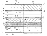
- FIG. 1 is a longitudinal sectional view showing a configuration of a flat panel X-ray detector (FPD), and FIG. 2 is a longitudinal sectional view in which a counter substrate is partially enlarged.
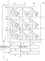
- FIG. 3 is a block diagram showing a configuration of a flat panel X-ray detector (FPD).
- the FPD 1 is generated with a counter substrate 3 having a polycrystalline semiconductor layer (hereinafter referred to as “semiconductor polycrystalline film”) 2 that generates charges (electron-hole pair carriers) in response to incident X-rays. And an active matrix substrate 4 for reading out the accumulated charges.
- semiconductor polycrystalline film a polycrystalline semiconductor layer (hereinafter referred to as “semiconductor polycrystalline film”) 2 that generates charges (electron-hole pair carriers) in response to incident X-rays.
- active matrix substrate 4 for reading out the accumulated charges.
- the counter substrate 3 supports, in order from the X-ray incident direction (symbol x in FIG. 1), a support substrate 5 that functions as a common electrode that supports the semiconductor polycrystalline film 2 and applies a negative bias voltage Vh, and a support substrate 5, an electron injection blocking layer 6 that blocks injection of charges (electrons) into the semiconductor polycrystalline film 2, a semiconductor polycrystalline film 2, and charges (holes) into the semiconductor polycrystalline film 2.
- the hole injection blocking layer 7 for blocking injection and the counter electrode 8 for collecting charges are stacked.
- the counter electrode 8 corresponds to an individual electrode of the present invention.
- a support substrate 5 is provided on one surface of the semiconductor polycrystalline film 2 via the electron injection blocking layer 6, and a matrix is provided for each pixel on the opposite side of the support substrate 5 across the semiconductor polycrystalline film 2.
- the counter electrode 8 is separately provided in a separate shape.
- the crystal grain size 9 of the semiconductor polycrystalline film 2 is configured to be smaller (finer) on the support substrate 5 side than on the counter electrode 8 side.
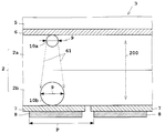
- the semiconductor polycrystalline film 2 includes a small grain polycrystalline region 2a on the support substrate 5 side and a large one on the counter electrode 8 side other than the small grain polycrystalline region 2a. It consists of a grain size polycrystalline region 2b.
- the small-grain-size polycrystalline region 2 a is a polycrystalline region that is initially (first) formed on the support substrate 5 via the electron injection blocking layer 6.
- the crystal grain size 9 of the semiconductor polycrystalline film 2 is configured to be smaller on the support substrate 5 side than on the counter electrode 8 side. That is, the crystal grain size 9 at almost both ends of the semiconductor polycrystalline film 2 on the support substrate 5 side and the counter electrode 8 side is configured to be smaller on the support substrate 5 side than on the counter electrode 8 side.
- the crystal grains in the small grain polycrystalline region 2a are denoted by reference numeral 10a, and the crystal grains in the large grain polycrystalline region 2b are denoted by reference numeral 10b.
- the small grain polycrystalline region 2a corresponds to the first polycrystalline film region of the present invention
- the large grain polycrystalline region 2b corresponds to the second polycrystalline film region of the present invention.
- the (average) crystal grain size 9 of the polycrystalline grains of the semiconductor polycrystalline film 2 is, for example, less than 50 ⁇ m on the support substrate 5 side when the pixel pitch (symbol P in FIG. 2) is 150 ⁇ m, and the counter electrode 8 side. That is, it is less than 150 ⁇ m (more desirably less than 75 ⁇ m) on the film surface side.
- the reason that the counter electrode 8 side has a crystal grain size 9 of less than 150 ⁇ m is that the pixel pitch P is 150 ⁇ m.
- the generated charges are collected at one counter electrode 8 in some cases.
- the light is collected by the other counter electrode 8 to cause variation among pixels. Therefore, for example, the crystal grain size 9 of the semiconductor polycrystalline film 2 is preferably smaller than the pixel pitch P on the counter electrode 8 side. Thereby, the dispersion
- the active matrix substrate 4 includes a capacitor 11 that stores the generated charge, a thin film transistor (TFT) 12 that functions as a switching element that reads the charge stored in the capacitor 11, and the like.
- the capacitor 11, the TFT 12, etc. are formed on the insulating substrate 13.
- the active matrix substrate 4 includes a pixel electrode 14 and a through hole 15.
- the capacitor 11 includes a capacitive electrode 16, an insulating film 17, and a ground line 18.
- the ground line 18 is grounded or a predetermined voltage set in advance is applied.
- the TFT 12 includes a capacitor electrode 16, an insulating film 17, a data line 19, a gate channel 20, and a gate line 21.
- the insulating film 22 is formed between the pixel electrode 14 and the capacitor electrode 16.
- the insulating film 23 is formed as a protective film.
- the counter substrate 3 and the active matrix substrate 4 are configured to be bonded together by bonding the counter electrode 8 of the counter substrate 3 and the pixel electrode 14 of the active matrix substrate 4 with the bump electrode 31.
- the X-ray detection elements DU are arranged in a two-dimensional matrix, and are composed of, for example, about 1500 ⁇ 1500 (about 230 ⁇ 230 mm). As shown in FIG. 3, the X-ray detection elements DU are configured by 3 ⁇ 3 for convenience of illustration.
- the capacitor 11 and the TFT 12 are individually provided in 3 ⁇ 3 X-ray detection elements DU configured in a two-dimensional matrix.
- the gate line 21 is configured to be commonly connected to the X-ray detection element DU in the row (X) direction, and the data line 19 is shared by the X-ray detection element DU in the column (Y) direction. Configured to connect to. Further, the gate line 21 is connected to the gate drive unit 33, and the data line 19 is connected to the charge voltage conversion amplifier 35 and the multiplexer 37 in order.
- the gate drive unit 33, the charge voltage conversion amplifier 35, and the multiplexer 37 are controlled by a drive control unit 39, and are driven by a signal from an external device (not shown), for example.
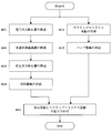
- Step S01 to S04 show a process of creating the counter substrate 3.
- Steps S ⁇ b> 11 and S ⁇ b> 12 show a process of creating the active matrix substrate 4 and a process of forming the bump electrode 31.
- the counter substrate 3 and the active matrix substrate 4 are bonded and integrated.
- the electron injection blocking layer 6 is formed on the support substrate 5 (the lower side in FIG. 1).
- the electron injection blocking layer 6 is made of a p-type semiconductor such as ZnTe (zinc telluride), Sb 2 S 3 (antimony sulfide), or Sb 2 Te 3 (antimony tellurium). Alternatively, they are formed by sputtering, chemical precipitation, or electrodeposition.
- the support substrate 5 preferably has a small X-ray absorption coefficient, and is made of, for example, a conductive material such as graphite, Al (aluminum), or SUS (stainless steel). If the support substrate 5 is made of an insulating material such as ceramic (Al 2 O 3 , AlN) or silicon, a common electrode (not shown) to which a bias voltage Vh is applied before the electron injection blocking layer 6 is formed. No) is formed on the support substrate 5, and the electron injection blocking layer 6 is formed on the formed common electrode.
- the common electrode is made of a conductive material such as ITO (indium tin oxide), Au (gold), Pt (platinum), or graphite, and is formed on the support substrate 5 by vapor deposition or sputtering.
- the semiconductor polycrystalline film 2 is formed on the electron injection blocking layer 6 by the proximity sublimation method.
- the semiconductor polycrystalline film 2 is composed of, for example, a polycrystalline film of CdTe or CdZnTe.
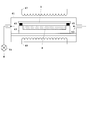
- FIG. 5 is a diagram for explaining the proximity sublimation method.
- a lower susceptor 43 for placing the source S is provided in the deposition chamber 41.
- the source S for example, a sintered body of a powder material of CdTe is used, and is sintered in advance by heating (for example, 690 ° C.) in an atmospheric pressure and an inert atmosphere (for example, Ar gas).
- the support substrate 5 is placed on the lower susceptor 43 in the vapor deposition chamber 41 with a spacer 45 interposed, with the vapor deposition surface on which the semiconductor polycrystalline film 2 is formed facing the lower susceptor 43.
- heaters 47 and 49 capable of independently controlling the temperature are provided on the upper and lower portions of the vapor deposition chamber 41.
- the vacuum pump 51 is operated to make the inside of the vapor deposition chamber 41 in a reduced pressure atmosphere (for example, 260 Pa), and then the source S is heated by the upper and lower heaters 47 and 49. (For example, substrate temperature 550 ° C., source temperature 650 ° C.). As a result, the source S sublimes and adheres to the vapor deposition surface of the electron injection blocking layer 6 to form the semiconductor polycrystalline film 2.
- the semiconductor polycrystalline film 2 may be doped with any impurity.
- the leakage current is reduced by widening the gap. Can be made.
- the carrier traveling property indicating the effect of making the crystal grain size 9 finer or the ease of charge flow at the crystal grain boundary of the semiconductor polycrystalline film 2 is improved, and the sensitivity and responsiveness are improved. Has the effect of improving.
- the semiconductor polycrystalline film 2 is formed on the support substrate 5 so that the crystal grain size 9 of the semiconductor polycrystalline film 2 is smaller on the support substrate 5 side than on the counter electrode 8 side.
- the step of forming the semiconductor polycrystalline film 2 includes the step of forming the small grain polycrystalline region 2a on the support substrate 5 via the electron injection blocking layer 6, and the step of forming the semiconductor polycrystalline film 2 on the small grain polycrystalline region 2a. And a step of forming a large grain size polycrystalline region 2b other than the small grain size polycrystalline region 2a.
- a small grain polycrystalline region 2 a is formed on the electron injection blocking layer 6.
- the small grain polycrystalline region 2a is formed while doping a predetermined amount (concentration) of Cl.
- the large grain polycrystalline region 2b is formed on the small grain polycrystalline region 2a.
- the large grain polycrystalline region 2b is formed without doping with Cl or with a smaller amount of Cl doped than in the small grain polycrystalline region 2a. It is preferable to form the semiconductor polycrystalline film 2 so that the crystal grain size 9 is smaller than the pixel pitch P (FIG. 2) on the counter electrode 8 side.
- Cl is mixed into the source S obtained by sintering the powder material, or Cl is supplied from the outside of the vapor deposition chamber 41 through the supply port 53.
- the source S includes a first material including at least one of CdTe, ZnTe, and CdZnTe, and a second material including at least one of CdCl 2 (cadmium chloride) and ZnCl 2 (zinc chloride). You may use the mixture of these.
- a Cl-containing gas obtained by diluting HCl (hydrogen chloride), CHCl 3 (chloroform) or the like with an inert gas such as argon (Ar) or nitrogen (N 2 ) is supplied from the outside to the inside of the deposition chamber 41.
- the flow rate may be supplied from the port 53 while being controlled.
- the source S mixed with Cl and a Cl-containing gas supplied from the outside to the inside of the vapor deposition chamber 41 may be combined.
- the semiconductor polycrystalline film 2 may be formed so that the (average) crystal grain size 9 changes continuously (stepwise) in the thickness direction 200, as indicated by reference numeral 61 in FIG.
- the amount of Cl (concentration) to be doped when forming the semiconductor polycrystalline film 2 is linear or curvilinear from a preset amount. It can be realized by reducing it to For example, when supplying a Cl-containing gas, the amount (concentration) of the supplied Cl is decreased stepwise from a preset amount, or in the case of the source S mixed with Cl, Cl disappears at the initial stage of film formation. It is also possible to reduce the Cl amount by utilizing the properties that are generated, or to reduce the Cl amount stepwise by combining them.
- the semiconductor polycrystalline film 2 is formed to a thickness of about 600 to 700 ⁇ m by the proximity sublimation method.
- the semiconductor polycrystalline film 2 is in an as-deposited state (as it is), the surface unevenness is as severe as several hundred ⁇ m, and the film thickness varies. Therefore, in order to integrally bond the surface of the semiconductor polycrystalline film 2 with the active matrix substrate 4, the semiconductor polycrystalline film 2 having a thickness of 600 to 700 ⁇ m is formed, and the surface is flattened by planar polishing and has a thickness of about 400 ⁇ m.
- the crystal grain size 9 is made smaller than the pixel pitch P on the counter electrode 8 side in the thickness of about 400 ⁇ m after the planar polishing.
- a hole injection blocking layer 7 is formed on the semiconductor polycrystalline film 2 (lower side in FIG. 1).
- the hole injection blocking layer 7 is made of an n-type semiconductor such as CdS (cadmium sulfide), ZnS (zinc sulfide), ZnO (zinc oxide), or Sb 2 S 3 (antimony sulfide). It is formed by sputtering, chemical precipitation, or electrodeposition.
- the hole injection blocking layer 7 is formed separately for each pixel by patterning as necessary. However, if the hole injection blocking layer 7 has a high resistance and there is no adverse effect such as a decrease in spatial resolution due to adjacent pixel leakage, it may not be formed separately.
- the arrangement of the electron injection blocking layer 6 and the hole injection blocking layer 7 may be exchanged, or one of the electron injection blocking layer 6 and the hole injection blocking layer 7 or It is good also as a structure which does not form both.
- the counter electrode 8 is formed on the hole injection blocking layer 7 (lower side in FIG. 1).
- the counter electrode 8 is made of a conductive material such as ITO, Au, Pt, or graphite, and is formed on the hole injection blocking layer 7 by vapor deposition or sputtering. In addition, it is good also as a structure which does not form the counter electrode 8 as needed. In this case, the bump electrode 31 functions as the counter electrode 8.
- Step S11 Creation of Active Matrix Substrate
- a ground line 18 and a gate line 21 are formed on an insulating substrate 13 made of glass or the like, and an insulating film 17 is formed so as to cover them.
- the ground line 18 and the gate line 21 are made of a metal film such as Ta (tantalum), Al (aluminum), or Mo (molybdenum), and are formed by vapor deposition or sputtering.
- the insulating film 17 is made of SiNx or SiOx and is formed by a vapor deposition method or the like.
- the insulating film 17 may be made of acrylic, polyimide, or the like in addition to the inorganic film.
- the gate channel 20 is formed on the insulating film 17.
- the gate channel 20 is formed of a-Si (amorphous silicon) or p-Si (polysilicon) formed by a vapor deposition method and diffused with impurities to form, for example, an n + layer.
- the capacitor electrode 16 and the data line 19 are formed on the insulating film 17 and the like, and the insulating film 22 is formed so as to cover them. Further, the through hole 15 is formed in the insulating film 22. Then, the pixel electrode 14 is formed on the insulating film 22 and the through hole 15, and the insulating film 23 is formed so as to open at the pixel electrode 14.
- the pixel electrode 14, the through hole 15, the capacitor electrode 16, and the data line 19 are made of a metal film such as Ta, Al, Ti (titanium). These metal films are formed by vapor deposition or sputtering.
- the insulating films 22 and 23 are made of SiNx or SiOx, like the insulating film 17, and are formed by vapor deposition or the like.
- Step S12 Formation of Bump Electrodes
- Bump electrodes 31 are formed on the active matrix substrate 4 formed in step S11.
- the bump electrode 31 is formed by screen printing a conductive paste.
- the bump electrode 31 is composed of a conductive paste.
- a conductive paste For example, an organic substance is gradually volatilized and cured by leaving a conductive material mainly composed of carbon and a conductive material mainly composed of carbon on a base material mainly composed of rubber. Or a blend of a binder resin that cures by condensation with moisture in the air.
- the electroconductive material contained in this electroconductive paste as long as it has electroconductivity, you may select a material suitably.
- the main component of the base material is exemplified as rubber, but other polymer materials may be used.
- binder resin it is not necessarily limited to resin, The mixture of the raw material which has adhesiveness and sclerosis
- the conductive paste includes, for example, a material such as a binder resin that is cured by allowing the organic substance to volatilize gradually when left at room temperature, or to cure by condensation with moisture in the air.
- a substance that cures when a temperature change (up to about 100 ° C.) is applied may be included.
- Step S21 Bonding of the counter substrate and the active matrix substrate
- the counter electrode 8 of the counter substrate 3 and the bump electrode 31 formed on the pixel electrode 14 of the active matrix substrate 4 are bonded. Thereby, the counter substrate 3 and the active matrix substrate 4 are bonded together.
- the joining is performed by leaving at room temperature or applying heat as necessary while applying a predetermined pressure set in advance.
- an anisotropic conductive film (ACF) may be used for bonding (connection).
- FPD1 is manufactured by the above process.
- a gate drive unit 33 a charge / voltage conversion amplifier 35, a multiplexer 37, a drive control unit 39, and the like are provided.
- the electric charge accumulated in the capacitor 11 is read from the capacitor 11 by the operation of the TFT 12.
- the gate driving unit 33 transmits the signals sequentially from the upper gate line 21 of FIG. 3 row by row, thereby bringing the TFT 12 into a connection (ON) state.
- the charge accumulated in the capacitor 11 is moved to the data line 19 through the TFT 12 and transferred to the charge-voltage conversion amplifier 35 through the data line 19.
- the charge-voltage conversion amplifier 35 converts the charge into a voltage, outputs it as a voltage signal, and transfers it to the multiplexer 37.
- the multiplexer 37 selects and outputs one voltage signal from the plurality of voltage signals. A two-dimensional X-ray image is acquired based on the output voltage signal.
- the semiconductor polycrystalline film is formed on the support substrate 5 so that the crystal grain size 9 of the semiconductor polycrystalline film 2 is smaller on the support substrate 5 side than on the counter electrode 8 side. 2 is formed. That is, the crystal grain size 9 of the semiconductor polycrystalline film 2 is smaller on the support substrate 5 side than on the counter electrode 8 side. Since the crystal grain size 9 on the side of the support substrate 5 formed earlier is small, it is possible to prevent the formation of through grains 201 (FIG. 7) in which crystal grain boundaries run vertically in the thickness direction 200 of the semiconductor polycrystalline film 2, Variations in sensitivity and leakage current of the semiconductor polycrystalline film 2 can be reduced. As a result, it is possible to obtain a radiation image with uniform sensitivity and leak current of each pixel, low pixel noise, and excellent diagnostic visibility.
- the crystal grain size 9 on the support substrate 5 side formed first (first) on the support substrate 5 through the electron injection blocking layer 6 is changed to the crystal formed on the counter electrode 8 side.
- the particle size 9 By forming smaller (finer) than the particle size 9, it is possible to prevent the formation of through grains.
- a crystal grain is grown to a large size, it grows to an equivalent size or larger than that, so it is relatively difficult to make the crystal grain small. Therefore, by first forming small crystal grains on the support substrate 5, the formation of the through grains 201 can be prevented and the size of the crystal grains can be controlled relatively easily.
- the step of forming the semiconductor polycrystalline film 2 includes the step of forming the small grain polycrystalline region 2a on the support substrate 5, and the formation of the large grain polycrystalline region 2b on the small grain polycrystalline region 2a.
- the small grain polycrystalline region 2a is formed while doping a predetermined amount (concentration) of Cl, and the large grain polycrystalline region 2b is formed without doping Cl or small grains. It is formed with a smaller amount of Cl to be doped than in the polycrystalline polycrystalline region 2a. Thereby, the crystal grain of the small grain polycrystalline region 2a on the support substrate 5 side can be made smaller than the large grain polycrystalline region 2b on the counter electrode 8 side.
- the crystal grain size 9 of the semiconductor polycrystalline film 2 is formed so as to continuously change in the thickness direction 200.
- the crystal grain size 9 of the semiconductor polycrystalline film 2 can be formed so as to continuously and greatly change in the thickness direction 200, that is, from the support substrate 5 side to the counter electrode 8 side.
- the stress in the semiconductor polycrystalline film 2 can be relieved, warpage of the support substrate 5 and cracks in the semiconductor polycrystalline film 2 can be suppressed.
- Example 2 of the present invention will be described.
- the small grain polycrystalline region 2a of the semiconductor polycrystalline film 2 is formed while doping a predetermined amount (concentration) of Cl, and the large grain polycrystalline film region 2b is doped with Cl. Or the amount of Cl to be doped is smaller than that of the small grain polycrystalline region 2a (FIGS. 1 and 2).
- the small grain polycrystalline region 2a is formed at a lower temperature than the large grain polycrystalline film region 2b.
- description of the part which overlaps with Example 1 is omitted.
- the step of forming the semiconductor polycrystalline film 2 includes the step of forming the small grain polycrystalline region 2a on the support substrate 5 via the electron injection blocking layer 6, and the step of forming the semiconductor polycrystalline film 2 on the small grain polycrystalline region 2a. And a step of forming a large grain size polycrystalline region 2b other than the small grain size polycrystalline region 2a.
- the small grain polycrystalline region 2a is formed at a lower temperature than the large grain polycrystalline film region 2b.
- the small grain polycrystalline region 2a is first formed in the range of 550 to 650 ° C., and the temperature of the heaters 47 and 49 shown in FIG. 2b is formed.
- the small grain polycrystalline region 2a is formed at a substrate temperature of 550 ° C. and a source temperature of 650 ° C.
- the large grain polycrystalline region 2b is formed at a substrate temperature of 600 ° C. and a source temperature of 700 ° C.
- the semiconductor polycrystalline film 2 may be formed such that the crystal grain size 9 continuously changes in the thickness direction 200. That is, the semiconductor polycrystalline film 2 is formed by changing the film formation temperature heated by the heaters 47 and 49 so as to increase linearly or continuously (stepwise) linearly or curvedly from a preset (low) temperature. Form.
- the step of forming the semiconductor polycrystalline film 2 includes the step of forming the small grain polycrystalline region 2a on the support substrate 5, and the small grain polycrystalline region 2a.
- a step of forming a large grain size polycrystalline region 2b, and the small grain size polycrystalline region 2a is formed at a temperature lower than that of the large grain size polycrystalline region 2b.
- the crystal grain size 9 of the semiconductor polycrystalline film 2 is formed so as to continuously change in the thickness direction 200. Thereby, the crystal grain size 9 of the semiconductor polycrystalline film 2 can be formed so as to continuously and greatly change in the thickness direction 200, that is, from the support substrate 5 side to the counter electrode 8 side.
- Example 1 or 2 when the semiconductor polycrystalline film 2 is formed, the small-crystal-sized polycrystalline region 2a and the large-grained polycrystalline film region 2b are formed by changing the Cl doping amount and temperature (see FIG. 1 and FIG. 2).
- Example 3 the small grain polycrystalline region 2a is formed at a higher pressure (low vacuum) than the large grain polycrystalline film region 2b.
- description of the part which overlaps with Example 1 and 2 is abbreviate
- the step of forming the semiconductor polycrystalline film 2 includes the step of forming the small grain polycrystalline region 2a on the support substrate 5 via the electron injection blocking layer 6, and the step of forming the semiconductor polycrystalline film 2 on the small grain polycrystalline region 2a. And a step of forming a large grain size polycrystalline region 2b other than the small grain size polycrystalline region 2a.
- the small grain polycrystalline region 2a is formed at a higher pressure than the large grain polycrystalline film region 2b.
- the semiconductor polycrystalline film 2 may be formed such that the crystal grain size 9 continuously changes in the thickness direction 200.
- the film formation pressure in the reduced-pressure atmosphere is changed by the vacuum pump 51 so as to decrease (increase the degree of vacuum) linearly or curve continuously (stepwise) from a preset (high) pressure.
- the semiconductor polycrystalline film 2 is formed.
- the step of forming the semiconductor polycrystalline film 2 includes the step of forming the small grain polycrystalline region 2a on the support substrate 5, and the small grain polycrystalline region 2a. Forming a large grain size polycrystalline region 2b on the top, and the small grain size polycrystalline region 2a is formed at a pressure higher than that of the large grain size polycrystalline region 2b. Thereby, the crystal grain of the small grain polycrystalline region 2a on the support substrate 5 side can be made smaller than the large grain polycrystalline region 2b on the counter electrode 8 side.
- the crystal grain size 9 of the semiconductor polycrystalline film 2 is formed so as to continuously change in the thickness direction 200. Thereby, the crystal grain size 9 of the semiconductor polycrystalline film 2 can be formed so as to continuously and greatly change in the thickness direction 200, that is, from the support substrate 5 side to the counter electrode 8 side.
- the present invention is not limited to the above embodiment, and can be modified as follows.
- the semiconductor polycrystalline film 2 is composed of CdTe or CdZnTe, that is, a polycrystalline film of a CdTe-based semiconductor or a CdZnTe-based semiconductor.
- the semiconductor polycrystalline film 2 can be applied to other than the polycrystalline film of CdTe semiconductor or CdZnTe semiconductor.
- the semiconductor polycrystalline film 2 generates charges in response to X-rays as radiation to be detected.
- X-rays it is not limited to X-rays, and may be, for example, ⁇ rays or light (visible light, ultraviolet rays, infrared rays, etc.).
- the FPD 1 can detect all of X-rays, ⁇ -rays, and light, but may be configured to detect at least one of X-rays, ⁇ -rays, and light.
- a two-dimensional X-ray image is detected.
- the X-ray image may be detected.
- the semiconductor polycrystalline film 2 when the semiconductor polycrystalline film 2 is formed, the Cl doping amount, temperature, and pressure are individually changed.
- the semiconductor polycrystalline film 2 may be formed by combining them. That is, the semiconductor polycrystalline film 2 may be formed by changing at least one of the conditions of the Cl doping amount, temperature and pressure.
Landscapes
- Physics & Mathematics (AREA)
- Health & Medical Sciences (AREA)
- Life Sciences & Earth Sciences (AREA)
- General Physics & Mathematics (AREA)
- High Energy & Nuclear Physics (AREA)
- Molecular Biology (AREA)
- Spectroscopy & Molecular Physics (AREA)
- Measurement Of Radiation (AREA)
- Solid State Image Pick-Up Elements (AREA)
- Transforming Light Signals Into Electric Signals (AREA)
Abstract
FPD1の製造方法において、半導体多結晶膜2の結晶粒径9を対向電極8側よりも支持基板5側で小さくなるように、支持基板5上に半導体多結晶膜2を形成する工程を備えている。すなわち、半導体多結晶膜2の結晶粒径9は、対向電極8側よりも支持基板5側で小さい。支持基板5側の先に形成される結晶粒径9が小さいので、半導体多結晶膜2の厚み方向200に結晶粒界が縦断するような貫通粒が形成されることを防止でき、半導体多結晶膜2の感度およびリーク電流のばらつきを低減させることができる。その結果、各画素の感度およびリーク電流が均一に揃い、画素ノイズの低い、診断上視認性の優れた放射線画像を取得することができる。
Description
本発明は、X線、γ線、光等を含む放射線を検出する機能を有し、医療用および異物検査等の産業用に使用される放射線検出器およびその製造方法に関する。
従来から高感度な放射線検出器の材料として各種の半導体材料、とりわけCdTe(テルル化カドミウム)またはCdZnTe(テルル化亜鉛カドミウム)の結晶体が研究・開発され、一部製品化されている。しかしながら、医用診断用の放射線検出器に応用するには、大面積(例えば20cm角以上)の放射線変換層を形成(成膜)する必要がある。このような大面積の結晶体を形成することは、技術的にもコスト的にも現実的に難しい。そこで、CdTeまたはCdZnTeの多結晶膜は、近接昇華法により形成されている(例えば特許文献1および2)。
従来の放射線検出器101を図6に示す。図6中の符号rは放射線の入射方向を示す。対向基板(検出基板ともいう)103は、放射線の入射側から順番に、バイアス電圧Vhが印加される共通電極として機能する導電性のグラファイト支持基板105、電子注入阻止層106、放射線に感応して電荷を生成する半導体層(放射線変換層)102、正孔注入阻止層107、対向電極108の各層(膜)が積層して構成されている。対向基板103は、バンプ電極131を介してアクティブマトリクス基板104と貼り合わせて一体的に構成されている。アクティブマトリクス基板104は、コンデンサ111およびスイッチング素子112を画素ごとに有し、入射した放射線強度に応じて半導体層102で生成された電荷を蓄積し、蓄積された電荷の読み出しを行っている。
なお、特許文献1には、多結晶の半導体層102、すなわち半導体多結晶膜102を形成する際、成膜温度を高くして粒径が大きい大粒径多結晶域を電子阻止用半導体膜(電子注入阻止層106)に積層形成する高温成膜過程を先に行い、次に成膜温度を低くして粒径が小さい小粒径多結晶膜を積層形成する低温成膜過程を行うことが開示されている。また、特許文献2には、Clが含まれたソースを用いて検出層(半導体多結晶膜)102の形成時にClをドープして結晶粒を均一化させ、検出層102が形成された後にさらにClをドープしてClを均一にドープさせることが開示されている。
しかしながら、このような従来例の場合には、次のような問題がある。放射線検出器101の半導体多結晶膜102では、膜質とりわけ膜の結晶構造(結晶粒の厚み方向200の分布)によって検出特性が大きく変化することがわかっている。具体的には、結晶粒径が大きいと、感度は向上するものの画素間のばらつきが大きくなり、リーク電流も半導体多結晶膜の厚み方向200に縦断する結晶粒界(結晶粒)の存否によって画素間のばらつきが非常に大きくなる。
図7に示すように、例えば、半導体多結晶膜102には、半導体多結晶膜102の厚み方向200を縦断するような結晶粒(以下適宜、「貫通粒」)がある場合(符号201)と、半導体多結晶膜102の厚み方向200に複数の結晶粒がある場合(符号202)とが混在しているものとする。結晶粒界は、半導体多結晶膜102の中でリーク電流の走行経路となるので、貫通粒201は、複数の結晶粒202に比べ、生成された電荷やリーク電流が流れ易くなる。そのため、対向電極108間、すなわち画素間でばらつきが生じ、また、流れ易さにより短い間隔で複数の画像(動画像)を取得する場合は、ゆらぎとなって現れる。その結果、放射線検出器101として画素ノイズが著しく増加し画質の劣化を招いてしまう。
本発明は、このような事情に鑑みてなされたものであって、リーク電流による画素間のばらつきを低減させることができる放射線検出器およびその製造方法を提供することを目的とする。
発明者は、上記の問題を解決するために鋭意研究した結果、次のような知見を得た。結晶粒径は初めに大きく成長すると、その結晶粒が同等の径かそれよりも大きく成長するので、半導体多結晶膜の厚み方向200に縦断する貫通粒201が生じやすい。そのため、半導体多結晶膜を初めに小さく結晶粒を形成する必要がある。
このような知見に基づく本発明は、次のような構成をとる。すなわち、本発明に係る放射線検出器の製造方法は、放射線に感応して電荷を生成する半導体多結晶膜と、前記半導体多結晶膜の一方の面に設けられた支持基板と、前記半導体多結晶膜を挟んで前記支持基板の反対側に画素ごとにマトリクス状に設けられた個別電極と、を備えた放射線検出器の製造方法において、前記半導体多結晶膜の結晶粒径を前記個別電極側よりも前記支持基板側で小さくなるように、前記支持基板上に前記半導体多結晶膜を形成する工程を備えていることを特徴とするものである。
本発明に係る放射線検出器の製造方法によれば、半導体多結晶膜の結晶粒径を個別電極側よりも支持基板側で小さくなるように、支持基板上に半導体多結晶膜を形成する工程を備えている。すなわち、半導体多結晶膜の結晶粒径は、個別電極側よりも支持基板側で小さい。先に形成される支持基板側の結晶粒径が小さいので、半導体多結晶膜の厚み方向に結晶粒界が縦断する貫通粒が形成されることを防止でき、半導体多結晶膜の感度およびリーク電流のばらつきを低減させることができる。その結果、各画素の感度およびリーク電流が均一に揃い、画素ノイズの低い、診断上視認性の優れた放射線画像を取得することができる。
また、本発明に係る放射線検出器の製造方法において、前記半導体多結晶膜の結晶粒径を前記個別電極側で画素ピッチよりも小さくなるように形成することが好ましい。これにより、複数の画素を結晶粒がまたぐことによる画素間のばらつきを低減することができる。
また、本発明に係る放射線検出器の製造方法において、前記半導体多結晶膜の一例は、CdTeまたはCdZnTeで構成されることである。これにより、CdTeまたはCdZnTeの多結晶膜の厚み方向に結晶粒界が縦断する貫通粒が形成されることを防止でき、CdTeまたはCdZnTeの多結晶膜の感度およびリーク電流のばらつきを低減させることができる。
また、本発明に係る放射線検出器の製造方法の一例は、前記半導体多結晶膜を形成する工程は、前記支持基板上に第1多結晶膜域を形成する工程と、第1多結晶膜域上に第2多結晶膜域を形成する工程とを有し、前記第1多結晶膜域は、予め設定されたCl量をドープしながら形成し、前記第2多結晶膜域は、前記第1多結晶膜域よりもドープさせるCl量を少なくして、またはClをドープさせずに形成することである。これにより、支持基板側の第1多結晶膜域の結晶粒を、個別電極側の第2多結晶膜域よりも小さくすることができる。
また、本発明に係る放射線検出器の製造方法の一例は、前記半導体多結晶膜を形成する工程は、前記支持基板上に第1多結晶膜域を形成する工程と、第1多結晶膜域上に第2多結晶膜域を形成する工程とを有し、前記第1多結晶膜域は、前記第2多結晶膜域よりも低い温度で形成することである。これにより、支持基板側の第1多結晶膜域の結晶粒を、個別電極側の第2多結晶膜域よりも小さくすることができる。
また、本発明に係る放射線検出器の製造方法の一例は、前記半導体多結晶膜を形成する工程は、前記支持基板上に第1多結晶膜域を形成する工程と、第1多結晶膜域上に第2多結晶膜域を形成する工程とを有し、前記第1多結晶膜域は、前記第2多結晶膜域よりも高い圧力で形成することである。これにより、支持基板側の第1多結晶膜域の結晶粒を、個別電極側の第2多結晶膜域よりも小さくすることができる。
また、本発明に係る放射線検出器の製造方法において、前記半導体多結晶膜の結晶粒径を厚み方向に連続的に変化するように形成することが好ましい。これにより、半導体多結晶膜の結晶粒径を厚み方向、すなわち、支持基板側から個別電極側へ連続的に大きく変化するように形成することができる。この場合、半導体多結晶膜の厚み方向、すなわち生成された電荷の進行方向に粒径の段差がなく、電荷をスムーズに移動させることができるので、応答性または感度等がより良好となる。また、半導体多結晶膜中の応力を緩和できるので、支持基板の反りや半導体多結晶膜のクラック等を抑えることができる。
また、本発明に係る放射線検出器は、放射線に感応して電荷を生成する半導体多結晶膜と、前記半導体多結晶膜の一方の面に設けられた支持基板と、前記半導体多結晶膜を挟んで前記支持基板の反対側に画素ごとにマトリクス状に設けられた個別電極と、を備え、前記半導体多結晶膜の結晶粒径は、前記個別電極側よりも前記支持基板側で小さいことを特徴とするものである。
本発明に係る放射線検出器によれば、半導体多結晶膜の結晶粒径は、個別電極側よりも支持基板側で小さい。先に形成される支持基板側の結晶粒径が小さいので、半導体多結晶膜の厚み方向に結晶粒界が縦断する貫通粒が形成されることを防止でき、半導体多結晶膜の感度およびリーク電流のばらつきを低減させることができる。その結果、各画素の感度およびリーク電流が均一に揃い、画素ノイズの低い、診断上視認性の優れた放射線画像を取得することができる。
また、本発明に係る放射線検出器において、前記半導体多結晶膜の結晶粒径は、前記個別電極側で画素ピッチよりも小さいことが好ましい。これにより、複数の画素を結晶粒がまたぐことによる画素間のばらつきを低減することができる。
本発明に係る放射線検出器およびその製造方法によれば、半導体多結晶膜の結晶粒径は、個別電極側よりも支持基板側で小さい。先に形成される支持基板側の結晶粒径が小さいので、半導体多結晶膜の厚み方向に結晶粒界が縦断する貫通粒が形成されることを防止でき、半導体多結晶膜の感度およびリーク電流のばらつきを低減させることができる。その結果、各画素の感度およびリーク電流が均一に揃い、画素ノイズの低い、診断上視認性の優れた放射線画像を取得することができる。
以下、図面を参照して本発明の実施例1を説明する。また、本実施例では、放射線検出器の一例として、フラットパネル型X線検出器(FPD)について説明する。図1は、フラットパネル型X線検出器(FPD)の構成を示す縦断面図であり、図2は、対向基板を部分拡大した縦断面図である。図3は、フラットパネル型X線検出器(FPD)の構成を示すブロック図である。
図1を参照する。FPD1は、入射したX線に感応して電荷(電子-正孔対キャリア)を生成する多結晶の半導体層(以下、「半導体多結晶膜」とする)2を有する対向基板3と、生成された電荷を蓄積するとともに蓄積された電荷を読み出すアクティブマトリクス基板4とを備えている。
対向基板3は、X線入射方向(図1中の符号x)から順番に、半導体多結晶膜2を支持するとともに負のバイアス電圧Vhを印加する共通電極として機能する支持基板5と、支持基板5の下面に形成され、半導体多結晶膜2への電荷(電子)の注入を阻止する電子注入阻止層6と、半導体多結晶膜2と、半導体多結晶膜2への電荷(正孔)の注入を阻止する正孔注入阻止層7と、電荷収集用の対向電極8と、が積層形成された構成となっている。なお、対向電極8は本発明の個別電極に相当する。
すなわち、半導体多結晶膜2の一方の面には、電子注入阻止層6を介して支持基板5が設けられ、半導体多結晶膜2を挟んで支持基板5の反対側には、画素ごとにマトリクス状に分離して個別に対向電極8が設けられている。また、半導体多結晶膜2の結晶粒径9は、対向電極8側よりも支持基板5側で小さく(細かく)なるように構成されている。
具体的には、図2に示すように、半導体多結晶膜2は、支持基板5側の小粒径多結晶域2aと、この小粒径多結晶域2a以外である対向電極8側の大粒径多結晶域2bとで構成されている。小粒径多結晶域2aは、電子注入阻止層6を介して支持基板5上に初め(先)に形成される多結晶域である。上述のように、半導体多結晶膜2の結晶粒径9は、対向電極8側よりも支持基板5側で小さくなるように構成されている。すなわち、支持基板5側と対向電極8側の半導体多結晶膜2のほぼ両端の結晶粒径9が、対向電極8側よりも支持基板5側で小さくなるように構成されている。なお、小粒径多結晶域2aの結晶粒を符号10aで示し、大粒径多結晶域2bの結晶粒を符号10bで示す。また、小粒径多結晶域2aは本発明の第1多結晶膜域に相当し、大粒径多結晶域2bは本発明の第2多結晶膜域に相当する。
半導体多結晶膜2の多結晶粒の(平均)結晶粒径9は、例えば、画素ピッチ(図2中の符号P)が150μmの場合、支持基板5側で50μm未満であり、対向電極8側、すなわち膜表面側で150μm未満(より望ましくは75μm未満)である。ここで、対向電極8側を150μm未満の結晶粒径9にするのは、画素ピッチPが150μmであるためである。例えば、複数(例えば2つ)の対向電極8(分離した正孔注入阻止層7)に結晶粒がまたがって形成された場合、生成された電荷が、ある時は一方の対向電極8で収集され、またある時は他方の対向電極8で収集されることにより、画素間でばらつきが生じる。そのため、例えば、半導体多結晶膜2の結晶粒径9は、対向電極8側で画素ピッチPよりも小さいことが好ましい。これにより、複数の画素を結晶粒がまたぐことによる画素間のばらつきを低減することができる。
図1に戻る。一方、アクティブマトリクス基板4は、生成された電荷を蓄積するコンデンサ11と、コンデンサ11に蓄積された電荷を読み出すスイッチング素子として機能する薄膜トランジスタ(TFT)12と等を備えている。コンデンサ11とTFT12等は、絶縁基板13上に形成されている。また、アクティブマトリクス基板4は、画素電極14およびスルーホール15を備えている。コンデンサ11は、容量電極16、絶縁膜17およびグランド線18とで構成されている。グランド線18は、アースされ、または、予め設定された所定電圧が印加されている。TFT12は、容量電極16および絶縁膜17、データ線19、ゲートチャネル20、ゲート線21で構成されている。また、絶縁膜22は、画素電極14と容量電極16との間に形成されている。絶縁膜23は保護膜として形成されている。
対向基板3とアクティブマトリクス基板4は、対向基板3の対向電極8とアクティブマトリクス基板4の画素電極14とがバンプ電極31で接合されることにより、貼り合わされて構成されている。
図1中の符号DUは、X線検出素子を示しており、X線検出素子DUでの検出が1画素に相当する。X線検出素子DUは、2次元マトリクス状に配置され、例えば1500×1500個程度(230×230mm程度)で構成される。X線検出素子DUは、図3に示すように、図示の便宜上3×3個で構成されている。コンデンサ11およびTFT12は、2次元マトリクス状に構成された3×3個のX線検出素子DUに個別に設けられている。
図3において、ゲート線21は、行(X)方向のX線検出素子DUで共通に接続するように構成されており、データ線19は、列(Y)方向のX線検出素子DUで共通に接続するように構成されている。また、ゲート線21は、ゲート駆動部33と接続しており、データ線19は、順番に電荷電圧変換アンプ35、マルチプレクサ37に接続している。ゲート駆動部33、電荷電圧変換アンプ35およびマルチプレクサ37は、駆動制御部39で制御されるようになっており、例えば図示しない外部装置からの信号で駆動される。
次に、FPD1の製造方法について、図4のフローチャートに沿って説明する。対向基板3とアクティブマトリクス基板4は、個別に作成される。ステップS01~S04は、対向基板3を作成する工程を示す。ステップS11、S12は、アクティブマトリクス基板4を作成する工程とバンプ電極31を形成する工程を示す。そして、ステップS21の工程において、対向基板3とアクティブマトリクス基板4とが貼り合わせて一体となる。
〔ステップS01〕電子注入阻止層の形成
支持基板5上(図1では下側)に電子注入阻止層6を形成する。電子注入阻止層6は、ZnTe(テルル化亜鉛)、Sb2S3(硫化アンチモン)、またはSb2Te3(アンチモンテルル)等のp型半導体で構成され、支持基板5上に昇華法、蒸着もしくはスパッタリング、化学析出法、または電析法等によって形成される。
支持基板5上(図1では下側)に電子注入阻止層6を形成する。電子注入阻止層6は、ZnTe(テルル化亜鉛)、Sb2S3(硫化アンチモン)、またはSb2Te3(アンチモンテルル)等のp型半導体で構成され、支持基板5上に昇華法、蒸着もしくはスパッタリング、化学析出法、または電析法等によって形成される。
なお、支持基板5は、X線の吸収係数が小さなものが好ましく、例えば、グラファイトや、Al(アルミニウム)、SUS(ステンレス)等の導電性材料で構成される。また、支持基板5がセラミック(Al2O3、AlN)や、シリコン等の絶縁材料で構成される場合は、電子注入阻止層6を形成する前に、バイアス電圧Vhを印加する共通電極(図示しない)を支持基板5上に形成し、形成された共通電極上に電子注入阻止層6を形成する。共通電極は、ITO(酸化インジウムスズ)や、Au(金)、Pt(白金)、グラファイトなどの導電性材料から構成され、支持基板5上に蒸着法やスパッタリング等で形成される。
〔ステップS02〕半導体多結晶膜の形成
電子注入阻止層6上に半導体多結晶膜2を近接昇華法により形成する。半導体多結晶膜2は、例えばCdTeまたはCdZnTeの多結晶膜で構成される。図5は、近接昇華法の説明に供する図である。
電子注入阻止層6上に半導体多結晶膜2を近接昇華法により形成する。半導体多結晶膜2は、例えばCdTeまたはCdZnTeの多結晶膜で構成される。図5は、近接昇華法の説明に供する図である。
蒸着チャンバ41内には、ソースSを置くための下部サセプタ43が設けられている。ソースSは、例えばCdTeの粉末材料の焼結体が用いられ、予め常圧かつ不活性雰囲気(例えばArガス)中で加熱(例えば690℃)して焼結させておく。支持基板5は、半導体多結晶膜2を形成する蒸着面を下部サセプタ43に向けた状態でスペーサ45を介在させて蒸着チャンバ41内の下部サセプタ43上に載置される。蒸着チャンバ41の上下部には、独立して温度を制御することが可能なヒータ47,49が設けられている。支持基板5とソースSとを対向配置させた状態で、真空ポンプ51を動作させて蒸着チャンバ41内を減圧雰囲気(例えば260Pa)にした後、上下部のヒータ47,49によりソースSを加熱する(例えば基板温度550℃、ソース温度650℃)。これにより、ソースSは昇華するとともに、電子注入阻止層6の蒸着面に付着して半導体多結晶膜2を形成する。
また、半導体多結晶膜2の検出特性を向上させるため、半導体多結晶膜2には、任意の不純物をドープしてもよく、例えば、Znをドープすると、ワイドギャップ化することによりリーク電流を低減させることができる。また、適量のClをドープすると、結晶粒径9を細かくする効果、または半導体多結晶膜2の結晶粒界等での電荷の流れ易さを示すキャリア走行性を改善し、感度および応答性を改善させる効果を有する。
本工程では、半導体多結晶膜2の結晶粒径9を対向電極8側よりも支持基板5側で小さくなるように、支持基板5上に半導体多結晶膜2を形成する。具体的には、半導体多結晶膜2を形成する工程は、電子注入阻止層6を介して支持基板5上に小粒径多結晶域2aを形成する工程と、小粒径多結晶域2a上に小粒径多結晶域2a以外の大粒径多結晶域2bを形成する工程とを有している。
まず、電子注入阻止層6上に小粒径多結晶域2aを形成する。小粒径多結晶域2aは、予め設定されたCl量(濃度)をドープしながら形成する。次に、小粒径多結晶域2a上に大粒径多結晶域2bを形成する。大粒径多結晶域2bは、Clをドープさせずに、または小粒径多結晶域2aよりもドープさせるCl量を少なくして形成する。なお、半導体多結晶膜2の結晶粒径9を対向電極8側で画素ピッチP(図2)よりも小さくなるように形成することが好ましい。
Clドープは、粉末材料を焼結させたソースSにClを混入したり、蒸着チャンバ41の外部から供給口53を通して内部にClを供給したりする。例えば、ソースSとしては、CdTe、ZnTe、およびCdZnTeの少なくとも1つを含む第1の材料と、CdCl2(塩化カドミウム)、およびZnCl2(塩化亜鉛)の少なくとも1つを含む第2の材料との混合体を用いてもよい。また、例えば、蒸着チャンバ41の外部から内部に、HCl(塩化水素)、CHCl3(クロロホルム)などをアルゴン(Ar)、窒素(N2)などの不活性ガスで希釈したCl含有ガスを、供給口53から流量を制御しながら供給してもよい。また、これらClを混入したソースSと、蒸着チャンバ41の外部から内部に供給するCl含有ガスとを組み合わせてもよい。
また、半導体多結晶膜2は、図2中の符号61に示すように、(平均)結晶粒径9が厚み方向200に連続的(段階的)に変化するように形成されてもよい。具体的には、半導体多結晶膜2(小粒径多結晶域2aおよび大粒径多結晶域2b)の形成時にドープさせるCl量(濃度)を、予め設定された量から直線的または曲線的に減少させることで実現させることができる。例えば、Cl含有ガスを供給する場合は、供給するCl量(濃度)を予め設定された量から段階的に減少させたり、Clを混入させたソースSの場合は、Clが成膜初期で無くなってしまう性質を利用してCl量を減少させたり、また、これらを組み合わせてCl量を段階的に減少させたりするようにしてもよい。
このようにして半導体多結晶膜2は、近接昇華法により600~700μm程度の厚みに形成する。半導体多結晶膜2がアズデポ(そのまま)の状態では、表面の凹凸が数百μmと激しく、また、膜厚にばらつきを有する。そのため、半導体多結晶膜2の表面をアクティブマトリクス基板4との一体化接合のため、600~700μmの半導体多結晶膜2を形成し、その表面を平面研磨して平坦化しするとともに400μm程度の厚みにする。なお、平面研磨後の400μm程度の厚みにおいて、結晶粒径9を対向電極8側で画素ピッチPよりも小さくする。
〔ステップS03〕正孔注入阻止層の形成
半導体多結晶膜2上(図1では下側)に正孔注入阻止層7を形成する。正孔注入阻止層7は、CdS(硫化カドミウム)、ZnS(硫化亜鉛)、ZnO(酸化亜鉛)、またはSb2S3(硫化アンチモン)等のn型半導体で構成され、昇華法、蒸着法、スパッタリング、化学析出法、または電析法等で形成される。正孔注入阻止層7は、必要に応じてパターニングして画素ごとに分離して形成する。但し、正孔注入阻止層7が高抵抗で隣接画素リークによる空間解像度低下などの弊害が無ければ、分離して形成しなくてもよい。
半導体多結晶膜2上(図1では下側)に正孔注入阻止層7を形成する。正孔注入阻止層7は、CdS(硫化カドミウム)、ZnS(硫化亜鉛)、ZnO(酸化亜鉛)、またはSb2S3(硫化アンチモン)等のn型半導体で構成され、昇華法、蒸着法、スパッタリング、化学析出法、または電析法等で形成される。正孔注入阻止層7は、必要に応じてパターニングして画素ごとに分離して形成する。但し、正孔注入阻止層7が高抵抗で隣接画素リークによる空間解像度低下などの弊害が無ければ、分離して形成しなくてもよい。
なお、必要に応じて、電子注入阻止層6と正孔注入阻止層7との配置を交換した構成としてもよいし、また、電子注入阻止層6および正孔注入阻止層7のいずれか一方あるいは両方を形成しない構成としてもよい。
〔ステップS04〕対向電極の形成
正孔注入阻止層7上(図1では下側)に対向電極8を形成する。対向電極8は、ITOや、Au、Pt、グラファイトなどの導電材料から構成され、正孔注入阻止層7上に蒸着法やスパッタリング等で形成される。なお、必要に応じて、対向電極8を形成しない構成としてもよい。なお、この場合、バンプ電極31が対向電極8として機能する。
正孔注入阻止層7上(図1では下側)に対向電極8を形成する。対向電極8は、ITOや、Au、Pt、グラファイトなどの導電材料から構成され、正孔注入阻止層7上に蒸着法やスパッタリング等で形成される。なお、必要に応じて、対向電極8を形成しない構成としてもよい。なお、この場合、バンプ電極31が対向電極8として機能する。
〔ステップS11〕アクティブマトリクス基板の作成
ガラス等で構成される絶縁基板13上にグランド線18とゲート線21とを形成し、それらを覆うように絶縁膜17を形成する。グランド線18およびゲート線21は、Ta(タンタル)、Al(アルミニウム)、Mo(モリブデン)等の金属膜で構成され、蒸着法またはスパッタリング等で形成される。絶縁膜17は、SiNxやSiOxで構成され、蒸着法等で形成される。また、絶縁膜17は、無機膜の他にアクリルやポリイミド等で構成してもよい。
ガラス等で構成される絶縁基板13上にグランド線18とゲート線21とを形成し、それらを覆うように絶縁膜17を形成する。グランド線18およびゲート線21は、Ta(タンタル)、Al(アルミニウム)、Mo(モリブデン)等の金属膜で構成され、蒸着法またはスパッタリング等で形成される。絶縁膜17は、SiNxやSiOxで構成され、蒸着法等で形成される。また、絶縁膜17は、無機膜の他にアクリルやポリイミド等で構成してもよい。
TFT12を形成するために、ゲートチャネル20を絶縁膜17上に形成する。ゲートチャネル20は、a-Si(アモルファスシリコン)やp-Si(ポリシリコン)を蒸着法で形成し、不純物を拡散させて例えばn+層としたもので構成される。
コンデンサ11およびTFT12を作成するために、容量電極16とデータ線19とを絶縁膜17等上に形成し、それらを覆うように絶縁膜22を形成する。また、絶縁膜22にスルーホール15を形成する。そして、絶縁膜22およびスルーホール15上に画素電極14を形成し、画素電極14で開口するように絶縁膜23を形成する。画素電極14、スルーホール15、容量電極16およびデータ線19は、Ta、Al、Ti(チタン)等の金属膜で構成される。これらの金属膜は、蒸着法またはスパッタリング等で形成される。絶縁膜22,23は、絶縁膜17と同様に、SiNxやSiOxで構成され、蒸着法等で形成される。
〔ステップS12〕バンプ電極の形成
ステップS11で形成されたアクティブマトリクス基板4上にバンプ電極31を形成する。バンプ電極31は、導電性ペーストをスクリーン印刷することにより形成される。
ステップS11で形成されたアクティブマトリクス基板4上にバンプ電極31を形成する。バンプ電極31は、導電性ペーストをスクリーン印刷することにより形成される。
バンプ電極31は、導電性ペーストで構成され、例えば、ゴムを主成分とした母材に、カーボンを主成分とした導電性材料と、常温で放置することにより有機物質が徐々に揮発して硬化する、あるいは空気中の水分と縮合反応して硬化するバインダー樹脂とを配合したもので構成される。この導電性ペーストに含まれる導電性材料については、導電性を有していれば、適宜材料を選択しても良い。また、例えば、母材の主成分をゴムと例示したが、その他の高分子材料でもよい。バインダー樹脂についても、必ずしも樹脂に限定されず、接着性および硬化性を有する素材の混合物であってもよい。
また、導電性ペーストには、例えば、バインダー樹脂のように常温で放置することにより有機物質が徐々に揮発して硬化する、あるいは空気中の水分と縮合反応して硬化する素材が含まれていることが望ましいが、温度変化(100℃程度まで)を与えることにより硬化する物質が含まれていてもよい。
〔ステップS21〕対向基板とアクティブマトリクス基板の貼り合わせ
対向基板3の対向電極8とアクティブマトリクス基板4の画素電極14上に形成されたバンプ電極31とを接合する。これにより、対向基板3とアクティブマトリクス基板4とが貼り合わされる。接合は、予め設定された所定の圧力を加えながら、常温放置、あるいは必要に応じて加熱することにより行われる。また、バンプ電極31以外にも、異方導電性フィルム(ACF)を用いて接合(接続)してもよい。
対向基板3の対向電極8とアクティブマトリクス基板4の画素電極14上に形成されたバンプ電極31とを接合する。これにより、対向基板3とアクティブマトリクス基板4とが貼り合わされる。接合は、予め設定された所定の圧力を加えながら、常温放置、あるいは必要に応じて加熱することにより行われる。また、バンプ電極31以外にも、異方導電性フィルム(ACF)を用いて接合(接続)してもよい。
以上の工程によりFPD1を製造する。なお、この他に、ゲート駆動部33、電荷電圧変換アンプ35、マルチプレクサ37、および駆動制御部39等が設けられる。
次に、図1および図3を参照してFPD1の動作を説明する。X線管から照射されたX線は被検体を透過し、被検体を透過したX線がFPD1に入射する(X線管と被検体は共に図示しない)。FPD1の半導体多結晶膜2にX線が入射されると、光導電効果により電荷が生成される。このとき、例えばグラファイト支持基板5には、負のバイアス電圧Vhが印加されているので、半導体多結晶膜2で生成された電荷は、バンプ電極31等を通じて画素ごとにコンデンサ11に蓄積される。
コンデンサ11に蓄積された電荷は、TFT12の動作によりコンデンサ11から読み出される。ゲート駆動部33は、例えば図3の上側のゲート線21から1行ずつ順番に信号を送信することで、TFT12を接続(ON)の状態にさせる。これにより、コンデンサ11に蓄積された電荷がTFT12を通じてデータ線19に移動され、データ線19を通じて電荷電圧変換アンプ35に転送される。電荷電圧変換アンプ35は、電荷を電圧に変換して電圧信号として出力し、マルチプレクサ37に転送する。マルチプレクサ37は、複数の電圧信号から1つの電圧信号を選択して出力する。出力された電圧信号に基づいて2次元のX線画像が取得される。
本実施例に係るFPD1およびその製造方法によれば、半導体多結晶膜2の結晶粒径9を対向電極8側よりも支持基板5側で小さくなるように、支持基板5上に半導体多結晶膜2を形成する工程を備えている。すなわち、半導体多結晶膜2の結晶粒径9は、対向電極8側よりも支持基板5側で小さい。先に形成される支持基板5側の結晶粒径9が小さいので、半導体多結晶膜2の厚み方向200に結晶粒界が縦断する貫通粒201(図7)が形成されることを防止でき、半導体多結晶膜2の感度およびリーク電流のばらつきを低減させることができる。その結果、各画素の感度およびリーク電流が均一に揃い、画素ノイズの低い、診断上視認性の優れた放射線画像を取得することができる。
半導体多結晶膜2の形成において、電子注入阻止層6を介して支持基板5上に初め(先)に形成される支持基板5側の結晶粒径9を、対向電極8側に形成される結晶粒径9よりも小さく(細かく)形成することで、貫通粒が形成されることを防止することができる。また、結晶粒を一度大きく成長させると、同等の大きさかそれよりも大きく成長するので、結晶粒を小さくすることは比較的に難しい。そこで、支持基板5上に初めに小さく結晶粒を形成することにより、貫通粒201の形成を防止するとともに結晶粒の大きさのコントロールを比較的容易に行える。
また、半導体多結晶膜2を形成する工程は、支持基板5上に小粒径多結晶域2aを形成する工程と、小粒径多結晶域2a上に大粒径多結晶域2bを形成する工程とを有し、小粒径多結晶域2aは、予め設定されたCl量(濃度)をドープしながら形成し、大粒径多結晶域2bは、Clをドープさせずに、または小粒径多結晶域2aよりもドープさせるCl量を少なくして形成する。これにより、支持基板5側の小粒径多結晶域2aの結晶粒を、対向電極8側の大粒径多結晶域2bよりも小さくすることができる。
また、半導体多結晶膜2の結晶粒径9は、厚み方向200に連続的に変化するように形成される。これにより、半導体多結晶膜2の結晶粒径9を厚み方向200、すなわち、支持基板5側から対向電極8側へ連続的に大きく変化するように形成することができる。この場合、半導体多結晶膜2の厚み方向200、すなわち生成された電荷の進行方向に粒径の段差がなく、電荷をスムーズに移動させることができるので、応答性または感度等がより良好となる。また、半導体多結晶膜2中の応力を緩和できるので、支持基板5の反りや半導体多結晶膜2のクラック等を抑えることができる。
次に、本発明の実施例2を説明する。実施例1において、半導体多結晶膜2の小粒径多結晶域2aは、予め設定されたCl量(濃度)をドープしながら形成し、大粒径多結晶膜域2bは、Clをドープさせずに、または小粒径多結晶域2aよりもドープさせるCl量を少なくして形成している(図1および図2)。しかしながら、実施例2では、小粒径多結晶域2aは、大粒径多結晶膜域2bよりも低い温度で形成する。なお、実施例1と重複する部分の説明は省略する。
上述のように、半導体多結晶膜2を形成する工程は、電子注入阻止層6を介して支持基板5上に小粒径多結晶域2aを形成する工程と、小粒径多結晶域2a上に小粒径多結晶域2a以外の大粒径多結晶域2bを形成する工程とを有している。ここで、小粒径多結晶域2aは、大粒径多結晶膜域2bよりも低い温度で形成される。例えば、550~650℃の範囲で小粒径多結晶域2aを先に形成し、図5に示すヒータ47,49の温度を高くして600~700℃の範囲で大粒径多結晶膜域2bを形成する。なお、この場合、例えば、小粒径多結晶域2aを基板温度550℃、ソース温度650℃で形成し、大粒径多結晶膜域2bを基板温度600℃、ソース温度700℃で形成する。
また、半導体多結晶膜2は、結晶粒径9が厚み方向200に連続的に変化するように形成されてもよい。すなわち、ヒータ47,49により加熱する成膜温度を、予め設定された(低い)温度から直線的または曲線的に連続的(段階的)に高くするように変化させることで半導体多結晶膜2を形成する。
本実施例に係るFPD1およびその製造方法によれば、半導体多結晶膜2を形成する工程は、支持基板5上に小粒径多結晶域2aを形成する工程と、小粒径多結晶域2a上に大粒径多結晶域2bを形成する工程とを有し、小粒径多結晶域2aは、大粒径多結晶域2bよりも低い温度で形成する。これにより、支持基板5側の小粒径多結晶域2aの結晶粒を、対向電極8側の大粒径多結晶域2bよりも小さくすることができる。
また、半導体多結晶膜2の結晶粒径9は、厚み方向200に連続的に変化するように形成される。これにより、半導体多結晶膜2の結晶粒径9を厚み方向200、すなわち、支持基板5側から対向電極8側へ連続的に大きく変化するように形成することができる。
次に、本発明の実施例3を説明する。実施例1または2において、半導体多結晶膜2の形成の際に、Clドープ量や温度を変化させて小粒径多結晶域2aおよび大粒径多結晶膜域2bを形成している(図1および図2)。しかしながら、実施例3では、小粒径多結晶域2aは、大粒径多結晶膜域2bよりも高い圧力(真空度の低い)で形成する。なお、実施例1および2と重複する部分の説明は省略する。
上述のように、半導体多結晶膜2を形成する工程は、電子注入阻止層6を介して支持基板5上に小粒径多結晶域2aを形成する工程と、小粒径多結晶域2a上に小粒径多結晶域2a以外の大粒径多結晶域2bを形成する工程とを有している。ここで、小粒径多結晶域2aは、大粒径多結晶膜域2bよりも高い圧力で形成する。例えば、2torrを基準として、5torrまたは10torrで小粒径多結晶域2aを先に形成し、図5に示す真空ポンプ51を動作させて圧力を低くして0.5torrまたは1torrで大粒径多結晶膜域2bを形成する。なお、1torr=130Paである。
また、半導体多結晶膜2は、結晶粒径9が厚み方向200に連続的に変化するように形成されてもよい。すなわち、真空ポンプ51により減圧雰囲気の成膜圧力を、予め設定された(高い)圧力から直線的または曲線的に連続的(段階的)に低くする(真空度を高くする)ように変化させることで半導体多結晶膜2を形成する。
本実施例に係るFPD1およびその製造方法によれば、半導体多結晶膜2を形成する工程は、支持基板5上に小粒径多結晶域2aを形成する工程と、小粒径多結晶域2a上に大粒径多結晶域2bを形成する工程とを有し、小粒径多結晶域2aは、大粒径多結晶域2bよりも高い圧力で形成する。これにより、支持基板5側の小粒径多結晶域2aの結晶粒を、対向電極8側の大粒径多結晶域2bよりも小さくすることができる。
また、半導体多結晶膜2の結晶粒径9は、厚み方向200に連続的に変化するように形成される。これにより、半導体多結晶膜2の結晶粒径9を厚み方向200、すなわち、支持基板5側から対向電極8側へ連続的に大きく変化するように形成することができる。
本発明は、上記実施形態に限られることはなく、下記のように変形実施することができる。
(1)上述した実施例では、半導体多結晶膜2は、CdTeまたはCdZnTe、すなわち、CdTe系半導体またはCdZnTe系半導体の多結晶膜で構成されていた。しかしながら、半導体多結晶膜2は、CdTe系半導体またはCdZnTe系半導体の多結晶膜以外でも応用可能である。
(2)上述した実施例および変形例(1)では、半導体多結晶膜2は、検出対象の放射線として、X線に感応して電荷を生成していた。しかしながら、X線に限らず、例えばγ線または光(可視光や紫外線、赤外線等)であってもよい。この場合、FPD1は、X線、γ線および光の全てを検出することが可能であるが、X線、γ線および光の少なくともいずれか1つを検出する構成であってもよい。
(3)上述した実施例および各変形例では、図3に示すように、2次元状のX線像を検出するものであったが、X線検出素子DUが1列に並ぶだけの1次元のX線像を検出するものであってもよい。
(4)上述した実施例および各変形例では、半導体多結晶膜2の形成の際に、Clドープ量や温度、圧力を個別に変化させていた。しかしながら、それらを組み合わせて半導体多結晶膜2を形成してもよい。すなわち、Clドープ量、温度および圧力の少なくとも1つの条件を変化させて半導体多結晶膜2を形成してもよい。
1 … フラットパネル型X線検出器(FPD)
2 … 多結晶の半導体層(半導体多結晶膜)
3 … 対向基板
4 … アクティブマトリクス基板
5 … 支持基板
8 … 対向電極
9 … 結晶粒径
41 … 蒸着チャンバ
47,49 … ヒータ
51 … 真空ポンプ
53 … 供給口
200 … 厚み方向
201 … 貫通粒
202 … 複数の結晶粒
P …画素ピッチ
2 … 多結晶の半導体層(半導体多結晶膜)
3 … 対向基板
4 … アクティブマトリクス基板
5 … 支持基板
8 … 対向電極
9 … 結晶粒径
41 … 蒸着チャンバ
47,49 … ヒータ
51 … 真空ポンプ
53 … 供給口
200 … 厚み方向
201 … 貫通粒
202 … 複数の結晶粒
P …画素ピッチ
Claims (9)
- 放射線に感応して電荷を生成する半導体多結晶膜と、
前記半導体多結晶膜の一方の面に設けられた支持基板と、
前記半導体多結晶膜を挟んで前記支持基板の反対側に画素ごとにマトリクス状に設けられた個別電極と、
を備えた放射線検出器の製造方法において、
前記半導体多結晶膜の結晶粒径を前記個別電極側よりも前記支持基板側で小さくなるように、前記支持基板上に前記半導体多結晶膜を形成する工程を備えていることを特徴とする放射線検出器の製造方法。 - 請求項1に記載の放射線検出器の製造方法において、
前記半導体多結晶膜の結晶粒径を前記個別電極側で画素ピッチよりも小さくなるように形成することを特徴とする放射線検出器の製造方法。 - 請求項1または2に記載の放射線検出器の製造方法において、
前記半導体多結晶膜は、CdTeまたはCdZnTeで構成されることを特徴とする放射線検出器の製造方法。 - 請求項1から3のいずれかに記載の放射線検出器の製造方法において、
前記半導体多結晶膜を形成する工程は、前記支持基板上に第1多結晶膜域を形成する工程と、第1多結晶膜域上に第2多結晶膜域を形成する工程とを有し、
前記第1多結晶膜域は、予め設定されたCl量をドープしながら形成し、
前記第2多結晶膜域は、前記第1多結晶膜域よりもドープさせるCl量を少なくして、またはClをドープさせずに形成することを特徴とする放射線検出器の製造方法。 - 請求項1から4のいずれかに記載の放射線検出器の製造方法において、
前記半導体多結晶膜を形成する工程は、前記支持基板上に第1多結晶膜域を形成する工程と、第1多結晶膜域上に第2多結晶膜域を形成する工程とを有し、
前記第1多結晶膜域は、前記第2多結晶膜域よりも低い温度で形成することを特徴とする放射線検出器の製造方法。 - 請求項1から5のいずれかに記載の放射線検出器の製造方法において、
前記半導体多結晶膜を形成する工程は、前記支持基板上に第1多結晶膜域を形成する工程と、第1多結晶膜域上に第2多結晶膜域を形成する工程とを有し、
前記第1多結晶膜域は、前記第2多結晶膜域よりも高い圧力で形成することを特徴とする放射線検出器の製造方法。 - 請求項1から6のいずれかに記載の放射線検出器の製造方法において、
前記半導体多結晶膜の結晶粒径を厚み方向に連続的に変化するように形成することを特徴とする放射線検出器の製造方法。 - 放射線に感応して電荷を生成する半導体多結晶膜と、
前記半導体多結晶膜の一方の面に設けられた支持基板と、
前記半導体多結晶膜を挟んで前記支持基板の反対側に画素ごとにマトリクス状に設けられた個別電極と、を備え、
前記半導体多結晶膜の結晶粒径は、前記個別電極側よりも前記支持基板側で小さいことを特徴とする放射線検出器。 - 請求項8に記載の放射線検出器において、
前記半導体多結晶膜の結晶粒径は、前記個別電極側で画素ピッチよりも小さいことを特徴とする放射線検出器。
Priority Applications (1)
| Application Number | Priority Date | Filing Date | Title |
|---|---|---|---|
| JP2013550077A JP5812112B2 (ja) | 2011-12-19 | 2012-10-22 | 放射線検出器およびその製造方法 |
Applications Claiming Priority (2)
| Application Number | Priority Date | Filing Date | Title |
|---|---|---|---|
| JP2011-277370 | 2011-12-19 | ||
| JP2011277370 | 2011-12-19 |
Publications (1)
| Publication Number | Publication Date |
|---|---|
| WO2013094099A1 true WO2013094099A1 (ja) | 2013-06-27 |
Family
ID=48668020
Family Applications (1)
| Application Number | Title | Priority Date | Filing Date |
|---|---|---|---|
| PCT/JP2012/006751 Ceased WO2013094099A1 (ja) | 2011-12-19 | 2012-10-22 | 放射線検出器およびその製造方法 |
Country Status (2)
| Country | Link |
|---|---|
| JP (1) | JP5812112B2 (ja) |
| WO (1) | WO2013094099A1 (ja) |
Cited By (1)
| Publication number | Priority date | Publication date | Assignee | Title |
|---|---|---|---|---|
| JP2015216271A (ja) * | 2014-05-12 | 2015-12-03 | 日本放送協会 | 固体撮像素子 |
Families Citing this family (1)
| Publication number | Priority date | Publication date | Assignee | Title |
|---|---|---|---|---|
| GB2531326B (en) * | 2014-10-16 | 2020-08-05 | Adaptix Ltd | An X-Ray emitter panel and a method of designing such an X-Ray emitter panel |
Citations (5)
| Publication number | Priority date | Publication date | Assignee | Title |
|---|---|---|---|---|
| JPH10294484A (ja) * | 1997-02-19 | 1998-11-04 | Canon Inc | 光起電力素子、光電変換素子、光起電力素子の製造方法及び光電変換素子の製造方法 |
| JP2001102602A (ja) * | 1999-09-30 | 2001-04-13 | Shimadzu Corp | アレイ型検出装置、およびその製造方法 |
| JP2002083946A (ja) * | 2000-09-07 | 2002-03-22 | Nippon Hoso Kyokai <Nhk> | イメージセンサ |
| JP2008153461A (ja) * | 2006-12-18 | 2008-07-03 | Hamamatsu Photonics Kk | 放射線検出器 |
| JP2008153460A (ja) * | 2006-12-18 | 2008-07-03 | Hamamatsu Photonics Kk | 放射線検出器 |
-
2012
- 2012-10-22 JP JP2013550077A patent/JP5812112B2/ja not_active Expired - Fee Related
- 2012-10-22 WO PCT/JP2012/006751 patent/WO2013094099A1/ja not_active Ceased
Patent Citations (5)
| Publication number | Priority date | Publication date | Assignee | Title |
|---|---|---|---|---|
| JPH10294484A (ja) * | 1997-02-19 | 1998-11-04 | Canon Inc | 光起電力素子、光電変換素子、光起電力素子の製造方法及び光電変換素子の製造方法 |
| JP2001102602A (ja) * | 1999-09-30 | 2001-04-13 | Shimadzu Corp | アレイ型検出装置、およびその製造方法 |
| JP2002083946A (ja) * | 2000-09-07 | 2002-03-22 | Nippon Hoso Kyokai <Nhk> | イメージセンサ |
| JP2008153461A (ja) * | 2006-12-18 | 2008-07-03 | Hamamatsu Photonics Kk | 放射線検出器 |
| JP2008153460A (ja) * | 2006-12-18 | 2008-07-03 | Hamamatsu Photonics Kk | 放射線検出器 |
Cited By (1)
| Publication number | Priority date | Publication date | Assignee | Title |
|---|---|---|---|---|
| JP2015216271A (ja) * | 2014-05-12 | 2015-12-03 | 日本放送協会 | 固体撮像素子 |
Also Published As
| Publication number | Publication date |
|---|---|
| JPWO2013094099A1 (ja) | 2015-04-27 |
| JP5812112B2 (ja) | 2015-11-11 |
Similar Documents
| Publication | Publication Date | Title |
|---|---|---|
| CN101517751B (zh) | 光或放射线检测器的制造方法及光或放射线检测器 | |
| JP4734597B2 (ja) | 放射線検出器の製造方法及び、放射線検出器並びに放射線撮像装置 | |
| US7301155B2 (en) | Radiation detector and radiation imaging apparatus and method for producing radiation detector | |
| JP2013142578A (ja) | 放射線検出器 | |
| EP2416177B1 (en) | Method of manufacturing radiation detector, radiation detector, and radiographic device | |
| JP5812112B2 (ja) | 放射線検出器およびその製造方法 | |
| CN103081127B (zh) | 放射线检测器的制造方法 | |
| JP5664798B2 (ja) | 放射線検出器とその製造方法 | |
| WO2012004913A1 (ja) | 放射線検出器およびそれを製造する方法 | |
| JP6061129B2 (ja) | 放射線検出器の製造方法 | |
| JP4092825B2 (ja) | アレイ型検出装置、およびその製造方法 | |
| WO2013088625A1 (ja) | 放射線検出器の製造方法 | |
| WO2013051174A1 (ja) | 放射線検出器およびその製造方法 | |
| JP5585733B2 (ja) | 放射線検出器およびその製造方法 | |
| JPWO2013065212A1 (ja) | 放射線検出器 | |
| JP2012194046A (ja) | 放射線検出器の製造方法 |
Legal Events
| Date | Code | Title | Description |
|---|---|---|---|
| 121 | Ep: the epo has been informed by wipo that ep was designated in this application |
Ref document number: 12859084 Country of ref document: EP Kind code of ref document: A1 |
|
| ENP | Entry into the national phase |
Ref document number: 2013550077 Country of ref document: JP Kind code of ref document: A |
|
| NENP | Non-entry into the national phase |
Ref country code: DE |
|
| 122 | Ep: pct application non-entry in european phase |
Ref document number: 12859084 Country of ref document: EP Kind code of ref document: A1 |