WO2013084629A1 - 表示装置および電子機器 - Google Patents
表示装置および電子機器 Download PDFInfo
- Publication number
- WO2013084629A1 WO2013084629A1 PCT/JP2012/078291 JP2012078291W WO2013084629A1 WO 2013084629 A1 WO2013084629 A1 WO 2013084629A1 JP 2012078291 W JP2012078291 W JP 2012078291W WO 2013084629 A1 WO2013084629 A1 WO 2013084629A1
- Authority
- WO
- WIPO (PCT)
- Prior art keywords
- layer
- display device
- electrode
- light emitting
- insulating layer
- Prior art date
- Legal status (The legal status is an assumption and is not a legal conclusion. Google has not performed a legal analysis and makes no representation as to the accuracy of the status listed.)
- Ceased
Links
Images


Classifications
-
- H—ELECTRICITY
- H10—SEMICONDUCTOR DEVICES; ELECTRIC SOLID-STATE DEVICES NOT OTHERWISE PROVIDED FOR
- H10K—ORGANIC ELECTRIC SOLID-STATE DEVICES
- H10K59/00—Integrated devices, or assemblies of multiple devices, comprising at least one organic light-emitting element covered by group H10K50/00
- H10K59/10—OLED displays
- H10K59/12—Active-matrix OLED [AMOLED] displays
- H10K59/122—Pixel-defining structures or layers, e.g. banks
-
- H—ELECTRICITY
- H10—SEMICONDUCTOR DEVICES; ELECTRIC SOLID-STATE DEVICES NOT OTHERWISE PROVIDED FOR
- H10K—ORGANIC ELECTRIC SOLID-STATE DEVICES
- H10K50/00—Organic light-emitting devices
- H10K50/10—OLEDs or polymer light-emitting diodes [PLED]
- H10K50/11—OLEDs or polymer light-emitting diodes [PLED] characterised by the electroluminescent [EL] layers
-
- H—ELECTRICITY
- H10—SEMICONDUCTOR DEVICES; ELECTRIC SOLID-STATE DEVICES NOT OTHERWISE PROVIDED FOR
- H10K—ORGANIC ELECTRIC SOLID-STATE DEVICES
- H10K50/00—Organic light-emitting devices
- H10K50/80—Constructional details
- H10K50/85—Arrangements for extracting light from the devices
- H10K50/858—Arrangements for extracting light from the devices comprising refractive means, e.g. lenses
-
- H—ELECTRICITY
- H10—SEMICONDUCTOR DEVICES; ELECTRIC SOLID-STATE DEVICES NOT OTHERWISE PROVIDED FOR
- H10K—ORGANIC ELECTRIC SOLID-STATE DEVICES
- H10K59/00—Integrated devices, or assemblies of multiple devices, comprising at least one organic light-emitting element covered by group H10K50/00
-
- H—ELECTRICITY
- H10—SEMICONDUCTOR DEVICES; ELECTRIC SOLID-STATE DEVICES NOT OTHERWISE PROVIDED FOR
- H10K—ORGANIC ELECTRIC SOLID-STATE DEVICES
- H10K59/00—Integrated devices, or assemblies of multiple devices, comprising at least one organic light-emitting element covered by group H10K50/00
- H10K59/80—Constructional details
- H10K59/875—Arrangements for extracting light from the devices
- H10K59/878—Arrangements for extracting light from the devices comprising reflective means
-
- H—ELECTRICITY
- H10—SEMICONDUCTOR DEVICES; ELECTRIC SOLID-STATE DEVICES NOT OTHERWISE PROVIDED FOR
- H10K—ORGANIC ELECTRIC SOLID-STATE DEVICES
- H10K50/00—Organic light-emitting devices
- H10K50/80—Constructional details
- H10K50/86—Arrangements for improving contrast, e.g. preventing reflection of ambient light
- H10K50/865—Arrangements for improving contrast, e.g. preventing reflection of ambient light comprising light absorbing layers, e.g. light-blocking layers
-
- H—ELECTRICITY
- H10—SEMICONDUCTOR DEVICES; ELECTRIC SOLID-STATE DEVICES NOT OTHERWISE PROVIDED FOR
- H10K—ORGANIC ELECTRIC SOLID-STATE DEVICES
- H10K59/00—Integrated devices, or assemblies of multiple devices, comprising at least one organic light-emitting element covered by group H10K50/00
- H10K59/80—Constructional details
- H10K59/8791—Arrangements for improving contrast, e.g. preventing reflection of ambient light
- H10K59/8792—Arrangements for improving contrast, e.g. preventing reflection of ambient light comprising light absorbing layers, e.g. black layers
Definitions
- the present technology relates to a display device and an electronic apparatus including a self-luminous element such as an organic EL (ElectroLuminescence) element.
- a self-luminous element such as an organic EL (ElectroLuminescence) element.
- an organic EL (ElectroLuminescence) element is a self-luminous display element and is excellent in terms of wide viewing angle, contrast, and response speed (for example, Patent Document 1).
- Such a self-luminous element such as an organic EL element has a first electrode, a functional layer including a light-emitting layer, and a second electrode on a substrate in this order, and adjacent elements are insulated layers (pixel division layers). ) Are separated from each other.
- a display device includes an insulating layer having an opening, a functional layer including a light emitting layer between the first electrode and the second electrode, and a light emitting element provided in the opening of the insulating layer.
- the insulating layer includes a low refractive index layer made of a constituent material having a lower refractive index than that of the functional layer close to the insulating layer.
- An electronic apparatus includes the display device.
- the insulating layer includes the low refractive index layer
- the light emitted from the light emitting layer is the wall surface of the opening (insulating layer including the low refractive index layer). It becomes easy to be totally reflected.
- the insulating layer includes the low refractive index layer, the light that is totally reflected by the insulating layer out of the light emitted from the light emitting layer.
- the amount of light can be increased. Therefore, light extraction efficiency is improved, and power consumption can be suppressed.
- FIG. 3 is a cross-sectional view illustrating a configuration of a display device according to a first embodiment of the present disclosure.
- FIG. It is the schematic showing the whole structure of the display apparatus shown in FIG.
- FIG. 3 is a circuit diagram illustrating an example of a pixel drive circuit illustrated in FIG. 2.
- FIG. 3 is a cross-sectional view illustrating a method of manufacturing the display device illustrated in FIG. 1 in order of steps.
- FIG. 8 is a cross-sectional view illustrating a method of manufacturing the display device illustrated in FIG. 7 in the order of steps. It is sectional drawing showing the process of following FIG. 8A. It is sectional drawing showing the structure of the display apparatus which concerns on a modification.
- FIG. 10 is a cross-sectional view illustrating a method of manufacturing the display device illustrated in FIG. 9 in the order of steps. It is sectional drawing showing the process of following FIG. 10A. It is a top view showing schematic structure of the module containing the display apparatus of the said embodiment. It is a perspective view showing the external appearance of the application example 1 of the display apparatus of the said embodiment. 10 is a perspective view illustrating an appearance of Application Example 2 viewed from the front side.
- FIG. 10 is a cross-sectional view illustrating a method of manufacturing the display device illustrated in FIG. 7 in the order of steps. It is sectional drawing showing the process of following FIG. 8A. It is sectional drawing showing the structure of the display apparatus which concerns on a modification.
- FIG. 14 is a perspective view illustrating an appearance of Application Example 2 viewed from the back side.
- FIG. 12 is a perspective view illustrating an appearance of application example 3.
- FIG. 14 is a perspective view illustrating an appearance of application example 4.
- FIG. It is a figure showing the closed state of the example 5 of application. It is a figure showing the open state of the example 5 of application.
- First embodiment an example in which the insulating layer is composed of a low refractive index layer
- Second embodiment an example in which the insulating layer is composed of a low refractive index layer and a black layer
- Modification example in which the insulating layer is composed of a low refractive index layer and a black layer, and the wall surface of the opening of the insulating layer is covered by the low refractive index layer
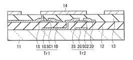
- FIG. 1 illustrates a cross-sectional configuration of a main part of a display device (display device 1) according to a first embodiment of the present technology.
- the display device 1 is a self-luminous display device including a plurality of organic light emitting elements 10, and includes a pixel drive circuit forming layer L1 and an organic light emitting element 10 on a support substrate 11 (first substrate).
- the element forming layer L2 and the counter substrate 18 (second substrate) are provided in this order.
- the display device 1 is a so-called top emission type display device having a light extraction direction on the counter substrate 18 side.
- the pixel drive circuit formation layer L1 includes, for example, a signal line drive circuit for image display and a scanning line drive circuit (see FIG. Not shown). Details of each component will be described later.
- FIG. 2 shows the overall configuration of the display device 1.
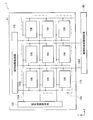
- the display device 1 has a display region 110 on a support substrate 11 and is used as an ultra-thin organic light emitting color display device or the like.
- a signal line driving circuit 120, a scanning line driving circuit 130, and a power supply line driving circuit 140 which are drivers for displaying images are provided.
- a plurality of organic light emitting elements 10 (10R, 10G, 10B) arranged two-dimensionally in a matrix and a pixel drive circuit 150 for driving them are formed.
- the organic light emitting elements 10R, 10G, and 10B mean the organic light emitting elements 10 that emit red, green, and blue, respectively.
- a plurality of signal lines 120A 120A1, 120A2,..., 120Am, etc.
- a plurality of power supply lines 140A 140A1,..., 140An,. ... Are arranged, and a plurality of scanning lines 130A (130A1,..., 130An,...) Are arranged in the row direction (X direction).
- any one of the organic light emitting elements 10R, 10G, and 10B is provided corresponding to each intersection of each signal line 120A and each scanning line 130A.
- Each signal line 120A has both ends connected to the signal line drive circuit 120
- each scanning line 130A has both ends connected to the scanning line drive circuit 130
- each power supply line 140A has both ends connected to the power supply line drive circuit 140. It is connected.
- the signal line driving circuit 120 supplies a signal voltage of a video signal corresponding to luminance information supplied from a signal supply source (not shown) to the selected organic light emitting elements 10R, 10G, and 10B via the signal line 120A. To do. A signal voltage from the signal line driver circuit 120 is applied to the signal line 120A from both ends thereof.
- the scanning line driving circuit 130 includes a shift register that sequentially shifts (transfers) the start pulse in synchronization with the input clock pulse.
- the scanning line driving circuit 130 scans them in units of rows when writing video signals to the organic light emitting elements 10R, 10G, and 10B, and sequentially supplies the scanning signals to the scanning lines 130A.
- a scanning signal from the scanning line driving circuit 130 is supplied to the scanning line 130A from both ends thereof.
- the power supply line driving circuit 140 includes a shift register that sequentially shifts (transfers) the start pulse in synchronization with the input clock pulse.
- the power supply line driving circuit 140 applies any one of the first potential and the second potential different from each other to each power supply line 140A in synchronization with the scanning in units of columns by the signal line driving circuit 120 as appropriate. Supply. Thereby, the conduction state or non-conduction state of the drive transistor Tr1 described later is selected.
- the pixel driving circuit 150 is provided in a layer between the substrate 11 and the organic light emitting element 10, that is, the pixel driving circuit forming layer L1.
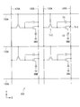
- FIG. 3 shows a configuration example of the pixel driving circuit 150.
- the pixel driving circuit 150 is an active driving circuit having a driving transistor Tr1 and a writing transistor Tr2, a capacitor (holding capacity) Cs therebetween, and the organic light emitting element 10.
- the organic light emitting element 10 is connected in series with the drive transistor Tr1 between the power supply line 140A and the common power supply line (GND).
- the driving transistor Tr1 and the writing transistor Tr2 are configured by a general thin film transistor (TFT (Thin Film Transistor)), and the configuration may be, for example, an inverted staggered structure (so-called bottom gate type) or a staggered structure (top gate type). Well not particularly limited.
- TFT Thin Film Transistor
- the drain electrode of the writing transistor Tr2 is connected to the signal line 120A, and the video signal from the signal line driving circuit 120 is supplied. Further, the gate electrode 2G of the writing transistor Tr2 is connected to the scanning line 130A, and a scanning signal is supplied from the scanning line driving circuit 130. Further, the source electrode 2S of the write transistor Tr2 is connected to the gate electrode 1G of the drive transistor Tr1.
- the drain electrode 1D is connected to the power supply line 140A and the drive transistor Tr1 is set to either the first potential or the second potential by the power supply line drive circuit 140.
- the source electrode 1S of the drive transistor Tr1 is connected to the organic light emitting element 10.
- the storage capacitor Cs is formed between the gate electrode 1G of the drive transistor Tr1 (source electrode 2S of the write transistor Tr2) and the drain electrode 1D of the drive transistor Tr1.
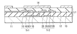
- the support substrate 11 is made of, for example, glass or plastic material that can block the permeation of moisture (water vapor) and oxygen. Since light is extracted from the counter substrate 18 in the top emission type, the support substrate 11 may be formed of either a transmissive material or a non-transmissive material. When the display device 1 is a flexible display, the support substrate 11 is preferably made of a flexible material such as a plastic material.
- the pixel drive circuit formation layer L1 has a laminated structure of the gate insulating film 12 and the planarization layer 13.
- a drive transistor Tr1 and a write transistor Tr2 constituting the pixel drive circuit 150 are formed, and further, a signal line 120A, a scanning line 130A, and a power supply line 140A (not shown) are also formed. Buried.
- the gate electrodes 1G and 2G of the drive transistor Tr1 and the write transistor Tr2 are formed on the support substrate 11 and are collectively covered with the gate insulating film 12.
- semiconductor layers SC1 and SC2 source electrodes 1S and 2S, and drain electrodes 1D and 2D in the drive transistor Tr1 and the write transistor Tr2 are formed, respectively.
- the gate electrodes 1G and 2G are formed of, for example, one or more of metal materials, inorganic conductive materials, organic conductive materials, and carbon materials.
- metal materials include aluminum (Al), copper (Cu), molybdenum (Mo), titanium (Ti), chromium (Cr), nickel (Ni), palladium (Pd), gold (Au), and silver (Ag). Platinum (Pt) or an alloy containing them.
- the inorganic conductive material include indium oxide (In 2 O 3 ), indium tin oxide (ITO), indium zinc oxide (IZO), and zinc oxide (ZnO).
- the organic conductive material is, for example, polyethylene dioxythiophene (PEDOT) or polystyrene sulfonic acid (PSS).
- the carbon material is, for example, graphite. Note that the gate electrodes 1G and 2G may be formed by stacking two or more layers of the various materials described above.
- the gate insulating film 12 is formed of one or more of an inorganic insulating material and an organic insulating material.
- the inorganic material include silicon oxide (SiO X ), silicon nitride (SiN X ), aluminum oxide (Al 2 O 3 ), titanium oxide (TiO 2 ), hafnium oxide (HfO X ), and barium titanate (BaTiO 3 ).
- Etc examples of the organic insulating material include polyvinylphenol (PVP), polyimide, polymethacrylic acid acrylate, photosensitive polyimide, photosensitive novolak resin, and polyparaxylylene. Note that the gate insulating film 12 may be formed by stacking two or more layers of the various materials described above.
- the semiconductor layers SC1 and SC2 are formed of one or more of inorganic semiconductor materials and organic semiconductor materials.
- the inorganic semiconductor material is, for example, amorphous silicon.
- As the organic semiconductor material for example, acene or a derivative thereof can be used.
- the acene is, for example, naphthacene, pentacene, hexacene, heptacene, dibenzopentacene, tetrabenzopentacene, pyrene, dibenzopyrene, chrysene, perylene, coronene, terylene, overene, quaterylene, or circumanthracene.
- the semiconductor layers SC1 and SC2 are preferably made of an organic semiconductor material.
- the source electrodes 1S, 2S and the drain electrodes 1D, 2D are made of, for example, the same material as the gate electrodes 1G, 2G described above, and are preferably in ohmic contact with the semiconductor layers SC1, SC2.
- the planarization layer 13 is provided mainly for planarizing the surface of the pixel drive circuit formation layer L1, and is formed of, for example, an insulating resin material such as polyimide.
- the source electrode and the drain electrode may be covered with a passivation layer made of a fluorinated polymer or the like, and the planarization layer 13 may be provided on the passivation layer.
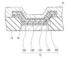
- the organic light emitting element 10 and the insulating layer 19 and a sealing layer 17 covering them are provided.
- the organic light emitting element 10 includes a first electrode 14 as an anode electrode, an organic layer 15 (functional layer) including a light emitting layer 15C (described later), and a second electrode 16 as a cathode electrode from the support substrate 11 side. They are stacked in order. The organic layer 15 and the first electrode 14 are separated for each organic light emitting element 10 by the insulating layer 19. On the other hand, the second electrode 16 is provided in common to all the organic light emitting elements 10.
- the first electrode 14 is an electrode that injects holes into the organic layer 15 (specifically, the hole transport layer 15A described later), and is formed on the planarizing layer 13 for each of the organic light emitting devices 10R, 10G, and 10B. Is provided.
- the first electrode 14 has a reflective surface on the surface facing the organic layer 15, and reflects the light emitted from the light emitting layer 15C toward the display surface side (second electrode 16 side). For this reason, it is preferable that the first electrode 14 has as high a reflectance as possible in order to increase the luminous efficiency.
- the first electrode 14 is made of a single element or alloy of a metal element such as silver (Ag), aluminum (Al), molybdenum (Mo), or chromium (Cr).
- the 1st electrode 14 as the laminated structure of the above-mentioned metal film and a transparent conductive film.
- the transparent conductive film include an oxide of indium and tin (ITO), indium zinc oxide (InZnO), an alloy of zinc oxide (ZnO) and aluminum (Al), and the like.
- the organic layer 15 is made of an organic material, and as shown in FIG. 4, from the first electrode 14 side, a hole injection layer 15A, a hole transport layer 15B, a light emitting layer 15C, an electron transport layer 15D, and an electron injection layer 15E. Are stacked in order. However, layers other than the light emitting layer may be provided as necessary.
- the hole injection layer 15A is a buffer layer for increasing hole injection efficiency and preventing leakage.
- the hole transport layer 15B is for increasing the efficiency of transporting holes to the light emitting layer 15C.
- the light emitting layer 15C generates light by applying an electric field to recombine electrons and holes.
- the electron transport layer 15D is provided to increase the electron transport efficiency to the light emitting layer 15C, and the electron injection layer 15E is provided to increase the electron injection efficiency.
- the electron injection layer 15E is made of, for example, LiF or Li 2 O.
- the hole injection layer 15A of the organic light emitting device 10R includes, for example, 4,4 ′, 4 ′′ -tris (3-methylphenylphenylamino) triphenylamine (m-MTDATA), 4,4 ′, 4 ′′ -tris (2 -Naphthylphenylamino) triphenylamine (2-TNATA), bis [(N-naphthyl) -N-phenyl] benzidine ( ⁇ -NPD), poly (3-hexylthiophene) (P3HT) or poly (3,4- Ethylenedioxythiophene): composed of poly (styrene sulfonate) (PEDOT-PSS).
- m-MTDATA 4,4 ′, 4 ′′ -tris (3-methylphenylphenylamino) triphenylamine
- 2-TNATA 4,4 ′, 4 ′′ -tris (2 -Naphthylphenylamino) triphen
- the hole transport layer 15B of the organic light emitting element 10R is made of, for example, ⁇ -NPD.
- the light emitting layer 15C of the organic light emitting device 10R includes, for example, 2,6-bis [4- [N- (4-methoxyphenyl) -N-phenyl] aminostyryl] naphthalene-1, 8-quinolinol aluminum complex (Alq 3 ), It is composed of 40% by volume of 5-dicarbonitrile (BSN-BCN).
- the electron transport layer 15D of the organic light emitting element 10R is made of, for example, Alq 3 .
- the hole injection layer 15A of the organic light emitting element 10G is made of, for example, m-MTDATA, 2-TNATA, ⁇ -NPD, P3HT, or PEDOT-PSS.
- the hole transport layer 15B of the organic light emitting device 10G is made of, for example, ⁇ -NPD.
- the light emitting layer 15C of the organic light emitting element 10G is made of, for example, Alq 3 mixed with 3% by volume of coumarin 6 (Coumarin 6).
- the electron transport layer 15D of the organic light emitting device 10G is made of, for example, Alq 3 .
- the hole injection layer 15A of the organic light emitting device 10B is made of, for example, m-MTDATA, 2-TNATA, ⁇ -NPD, P3HT, or PEDOT-PSS.
- the hole transport layer 15B of the organic light emitting device 10B is made of, for example, ⁇ -NPD.
- the light emitting layer 15C of the organic light emitting element 10B is composed of, for example, spiro 6 ⁇ .
- the electron transport layer 15D of the organic light emitting element 10B is made of, for example, Alq 3 .
- the second electrode 16 is provided on the organic layer 15 in a state insulated from the first electrode 14 in common to the organic EL elements 10R, 10G, and 10B.
- the second electrode 16 is made of a light transmissive transparent material, for example, indium tin oxide (ITO), zinc oxide (ZnO), alumina doped zinc oxide (AZO), gallium doped zinc oxide (GZO), indium zinc oxide. (IZO), indium titanium oxide (ITiO), indium tungsten oxide (IWO), or the like.
- the insulating layer 19 has an opening 19M, and the first electrode 14, the organic layer 15, and the second electrode 16 are in contact with each other in the opening 19M to form a stacked structure thereof. That is, the organic light emitting device 10 (organic light emitting devices 10R, 10G, and 10B) is provided in the opening 19M, and the light emitting region is defined by the opening 19M. A part of the insulating layer 19 is in contact with the surface of the first electrode 14, and the wall surface (side surface) of the opening 19 ⁇ / b> M is inclined (inclination angle ⁇ ) with respect to the surface of the first electrode 14.
- the tilt angle ⁇ is arbitrary and may be any of acute, right angle, and obtuse, but in the display device 1 in which the second electrode 16 side is in the light extraction direction, the tilt angle ⁇ is preferably an acute angle. This is because if the inclination angle ⁇ is an acute angle, the opening 19M widens toward the second electrode 16 and the light extraction efficiency is improved.
- the organic layer 15 is provided along the wall surface and bottom surface of the opening 19M of the insulating layer 19, and the lowermost layer (hole injection layer 15A) of the organic layer 15 is in contact with the wall surface of the opening 19M.
- the planar shape of the opening 19M is, for example, a square shape, but the shape of the opening 19M is arbitrary, and may be, for example, a slit shape or a U-shape.
- the insulating layer 19 is composed of a layer closest to the insulating layer 19 in the organic layer 15, that is, a low refractive index layer made of a material having a refractive index lower than that of the constituent material of the hole injection layer 15A.
- the insulating layer 19 only needs to be at least partially constituted by a low refractive index layer, and it is preferable that the low refractive index layer and the hole injection layer 15A are in contact with each other.
- the insulating layer 19 is composed of only a low refractive index layer.
- the refractive index of the constituent material of the insulating layer 19 is n1
- the refractive index of the constituent material of the hole injection layer 15A is n2, n1 ⁇ n2.
- the insulating layer 19 it is preferable to adjust the refractive index n1 and the inclination angle ⁇ of the constituent material so that most of the light generated in the light emitting layer 15C is totally reflected by the wall surface of the opening 19M.
- the hole injection layer 15A is made of NPD (MoO 3 co-deposited film (20% doped)), P3HT, or PEDOT / PSS
- the insulating layer 19 is made of fluorinated polyimide.
- the refractive index of ⁇ -NPD is 1.8
- the refractive index of P3HT is 1.95.
- the insulating layer 19 made of polyimide is preferably adjusted to a refractive index of less than 1.5 by controlling the refractive index by fluorination.
- the sealing layer 17 is formed of an insulating resin material such as polyimide, for example, similarly to the planarization layer 13.
- the counter substrate 18 seals the organic light emitting element 10 together with the sealing layer 17 and an adhesive layer (not shown) such as a thermosetting resin, and is generated in the light emitting layer 15 ⁇ / b> C included in the organic layer 15. It is made of transparent glass or plastic material that transmits light.
- the counter substrate 18 is preferably made of a flexible material such as a plastic material. This is because such a counter substrate 18 is harder to break than a case where it is made of glass or the like, and can increase the resistance to impact. Further, since the counter substrate 18 made of a flexible material can be provided with a barrier film having a barrier property against oxygen and water, the reliability of the display device 1 can be improved.
- the display device 1 can be manufactured as follows, for example.
- the pixel drive circuit formation layer L1 and the first electrode 14 are formed on the support substrate 11. Specifically, first, a metal film made of a constituent material of the gate electrodes 1G and 2G is formed on the support substrate 11 by, for example, vapor deposition. Thereafter, the metal film is patterned by, for example, photolithography, dry etching, or wet etching, thereby forming the gate electrodes 1G and 2G and the signal line 120A on the support substrate 11. Next, the gate insulating film 12 is formed by spin coating or the like using the above material so as to cover the entire surface of the support substrate 11.
- the semiconductor layers SC1 and SC2, the drain electrodes 1D and 2D, and the source electrodes 1S and 2S are sequentially formed on the gate insulating film 12 using a vapor deposition method and a photolithography method, for example, in a predetermined shape. .
- a connecting portion for connecting the gate electrode 1G and the source electrode 2S is formed in the gate insulating film 12 in advance.
- the scanning line 130A and the power supply line 140A are formed. At that time, necessary connection portions for connecting each wiring and each electrode are appropriately formed.
- the pixel drive circuit formation layer L1 is completed by covering the entire surface with the planarization layer 13 by spin coating or the like (by further performing a photolithography process if necessary).
- a connection hole for forming a connection portion with the first electrode 14 is formed at a predetermined position on the metal layer 1S in the planarization layer 13 by dry etching or the like.
- the first electrode 14 made of the predetermined material described above is formed. Specifically, for example, a metal film made of the above-described material is formed on the entire surface by, for example, vapor deposition, and then a resist pattern (not shown) having a predetermined shape is formed on the metal film using a predetermined mask. Using the resist pattern as a mask, the metal film is selectively etched. At that time, the first electrode 14 is formed so as to cover the surface of the planarization layer 13 and fill the connection hole.
- the insulating layer 19 is formed by patterning as shown in FIG. 5B. Specifically, the constituent material of the insulating layer 19 is applied to the entire surface of the substrate 11 (on the planarizing layer 13 and the first electrode 14) by a spin coating method. Thereafter, baking, selective exposure, and development are sequentially performed, so that patterning into a predetermined shape having the opening 19M can be performed.
- the hole injection layer 15A, the hole transport layer 15B, the light emitting layer 15C, the electron transport layer 15D, and the electron injection layer 15E having the predetermined materials and thicknesses described above so as to completely cover the opening 19M are formed by, for example, vapor deposition.
- the organic layer 15 is formed by sequentially laminating.
- the second electrode 16 is formed over the entire surface so as to face the first electrode 14 with the organic layer 15 in between, for example, using an evaporation method. Thereby, the organic light emitting element 10 is formed.
- the organic layer 15 and the second electrode 16 are preferably formed by a method excellent in film thickness control, for example, a vapor deposition method. By accurately controlling the film thicknesses of the organic layer 15 and the second electrode 16, multiple interference of the organic light emitting element 10 between the first electrode 14 and the second electrode 16 can be used. And the color filter can be omitted.
- the sealing layer 17 is formed on the entire surface of the substrate 11. Finally, the counter substrate 18 is bonded to the sealing layer 17 with, for example, a vacuum lamination method with an adhesive layer interposed therebetween, and the display device 1 is completed.
- each organic light emitting element 10 is supplied with a scanning signal from the scanning line driving circuit 130 via the gate electrode 2 G of the writing transistor Tr 2, and an image signal is written from the signal line driving circuit 120 to the writing transistor. It is held in the holding capacitor Cs via Tr2. That is, the driving transistor Tr1 is controlled to be turned on / off according to the signal held in the holding capacitor Cs, whereby a driving current is injected into the organic light emitting element 10, and holes and electrons are recombined to emit light. This light passes through the second electrode 16, the sealing layer 17 and the counter substrate 18 and is extracted.
- the refractive index n1 of the constituent material of the insulating layer 19 is made smaller than the refractive index n2 of the constituent material of the hole injection layer 15A (n1 ⁇ n2), as shown in FIG.
- the generated light is easily totally reflected by the wall surface of the opening 19M of the insulating layer 19. That is, among the light emitted from the light emitting layer 15C, the amount of light transmitted through the insulating layer 19 in the X-axis direction is reduced, and the amount of light emitted toward the counter substrate 18 (Z-axis direction) is increased. Therefore, the light extraction efficiency can be improved.
- the refractive index n1 of the insulating layer 19 is made smaller than the refractive index n2 of the hole injection layer 15A, the light extraction efficiency can be improved and the power consumption can be suppressed. It becomes possible.
- FIG. 7 illustrates a cross-sectional configuration of a main part of a display device (display device 2) according to the second embodiment of the present technology.
- the insulating layer 29 has a laminated structure of a low refractive index layer 29A and a black layer 29B. Except for this point, the display device 2 has the same configuration as the display device 1 of the first embodiment, and the operation and effect thereof are also the same.
- the insulating layer 29 has a low refractive index layer 29A and a black layer 29B in this order from the first electrode 14 side.
- an opening 29 ⁇ / b> M is provided in the same manner as the insulating layer 19 of the display device 1.
- the low refractive index layer 29A is made of the same constituent material (refractive index n1) as that of the insulating layer 19.
- the black layer 29B is made of, for example, a material that exhibits black color by dispersing black pigment, dye, and pigment in an insulating resin material such as polyimide, that is, a material that absorbs visible light and reduces reflection. Yes.
- substrate 18 side is absorbed by the black layer 29B, reflection by the 1st electrode 14 of this external light, ie, external light reflection, can be suppressed. Therefore, the light extraction efficiency can be increased by the low refractive index layer 29A, and the visibility of the display image of the display device 2 can be improved by the black layer 29B.
- the external light reflectance in the organic light emitting device 10 can be further reduced by a combination with a retardation plate or a polarizing plate (not shown).
- the pixel separation is performed by the insulating layer 29 including the black layer 29B, it is possible to avoid mixing (mixing of colors) image light of different colors from the adjacent organic light emitting elements 10R, 10G, and 10B. .
- the black layer 29B can realize a high-definition and high-contrast display image without performing such alignment.
- the counter substrate 18 is made of a flexible substrate such as plastic, the alignment work becomes difficult from the viewpoint of dimensional stability, flatness, handling property (handling property), and the like. Instead of this, it is preferable to increase the contrast with the black layer 29B.
- the black pigment contained in the black layer 29B for example, at least one of the following organic pigments and inorganic pigments is used.
- the organic pigment include azo lake, insoluble azo, condensed azo, phthalocyanine, quinacridone, dioxazine, isoindolinone, anthraquinone, perinone, thioindico, and perylene.
- the inorganic pigment include carbon black, titanium oxide, miloli blue, cobalt violet, manganese violet, ultramarine blue, bitumen, cobalt blue, cerulean blue, and viridian. These pigments can be used alone or in admixture of two or more.
- black dyes examples include nigrosine (for example, NUbian BLACK (registered trademark) series manufactured by Orient Chemical Industries) and BONJET BLACK (registered trademark) (produced by Orient Chemical Industries), which are azine compounds condensed with aniline and nitrobenzene.
- nigrosine for example, NUbian BLACK (registered trademark) series manufactured by Orient Chemical Industries
- BONJET BLACK registered trademark
- the low-refractive index layer 29A and the black layer 29B are formed using a photosensitive resin material that can be molded by photopatterning or reflowing, etc., in order to simplify the forming process and enable molding into a desired shape. Is preferred.
- the display device 2 first, after the pixel drive circuit formation layer L 1 and the first electrode 14 are formed on the support substrate 11 in the same manner as the display device 1 (FIG. 8A), as shown in FIG. 29 is formed.
- the insulating layer 29 is formed by depositing the constituent material of the low refractive index layer 29A and the constituent material of the black layer 29B in this order on the entire surface of the substrate 11 (on the first electrode 14 and the gate insulating layer 13) by, for example, spin coating. Thereafter, patterning is performed. At this time, for example, when a positive type black resist containing a black pigment is used for the black layer 29B, this is formed on the entire surface of the substrate 11, then baked (for example, at 100 ° C.
- the insulating layer 29 has a laminated structure of the low refractive index layer 29A and the black layer 29B, it can be formed by a single lithography process similar to the insulating layer 19.
- the organic layer 15, the second electrode 16, and the sealing layer 17 are formed in the same manner as the display device 1.
- the pixel drive circuit formation layer L1 and the light emitting element formation layer L2 are formed on the support substrate 11.
- the display device 2 is completed by bonding the support substrate 11 provided with the pixel drive circuit formation layer L1 and the light emitting element formation layer L2 and the counter substrate 18 together.
- the conventionally used black matrix is not necessary, so that the number of manufacturing steps can be reduced and the cost can be reduced.
- the constituent material of the light emitting layer 15C is common to the organic light emitting elements 10R, 10G, and 10B, light of the same color (for example, white) is emitted from the organic light emitting elements 10R, 10G, and 10B.
- different colors of light are extracted from each pixel by providing different color filters for the respective organic light emitting elements 10R, 10G, and 10B.
- such a color filter can be provided in the light emitting element formation layer L2.
- a protective layer made of, for example, SiN x , SiO x, or AlO is formed on the entire surface of the second electrode 16 by a sputtering method or a vacuum process such as CVD (Chemical Vapor Deposition).
- the protective layer may be formed by laminating the inorganic film, or may be laminated with an organic film.
- a color filter is formed on the protective layer so as to correspond to each of the organic light emitting elements 10R, 10G, and 10B, and then a sealing layer 17 is formed. That is, since it is not necessary to form a color filter on the counter substrate 18, the counter substrate 18 can be bonded to the support substrate 11 without performing a precise alignment operation.
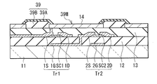
- FIG. 9 illustrates a cross-sectional configuration of a main part of a display device (display device 2A) according to a modification of the second embodiment.
- the wall surface of the opening 39M of the insulating layer 39 is covered with the low refractive index layer 39A. Except for this point, the display device 2A has the same configuration as the display device 2, and the operation and effect thereof are also the same.
- the insulating layer 39 has a black layer 39B and a low refractive index layer 39A in this order from the first electrode 14 side, and the wall surface of the opening 39M is covered with the low refractive index layer 39A.
- Layer 39 is formed.
- the insulating layer 39 is formed by first applying the constituent material of the black layer 39B to the entire surface of the substrate 11 (on the first electrode 14 and the gate insulating layer 13) and then patterning to form the black layer 39B.
- the low refractive index layer 39A is formed so as to cover the black layer 39B.
- the display devices 1, 2, and 2A according to the above-described embodiments are generated from an externally input video signal, such as a television device, a digital camera, a notebook personal computer, a mobile terminal device such as a mobile phone, or a video camera.
- This video signal can be applied to display devices of electronic devices in all fields that display images or videos.
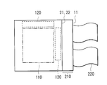
- the display device of the above-described embodiment or the like is incorporated into various electronic devices such as application examples 1 to 5 described later, for example, as a module shown in FIG.
- a region 210 exposed from the sealing layer 17 and the counter substrate 18 is provided on one side of the support substrate 11, and wirings of the signal line driving circuit 120 and the scanning line driving circuit 130 are provided in the exposed region 210.
- An external connection terminal (not shown) is formed by extending.
- the external connection terminal may be provided with a flexible printed circuit (FPC) 220 for signal input / output.
- FPC flexible printed circuit
- FIG. 12 illustrates an appearance of a television device to which the display device of the above-described embodiment or the like is applied.
- This television apparatus has, for example, a video display screen unit 300 including a front panel 310 and a filter glass 320, and the video display screen unit 300 is configured by the display device according to the above embodiment.
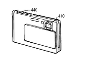
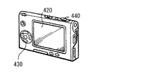
- FIG. 13A and 13B show the appearance of a digital camera to which the display device of the above-described embodiment or the like is applied.
- the digital camera includes, for example, a flash light emitting unit 410, a display unit 420, a menu switch 430, and a shutter button 440, and the display unit 420 is configured by the display device according to the above embodiment. .
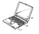
- FIG. 14 illustrates an appearance of a notebook personal computer to which the display device of the above-described embodiment or the like is applied.
- the notebook personal computer has, for example, a main body 510, a keyboard 520 for inputting characters and the like, and a display unit 530 for displaying an image.
- the display unit 530 is a display device according to the above embodiment. It is comprised by.
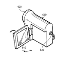
- FIG. 15 shows the appearance of a video camera to which the display device of the above embodiment is applied.
- This video camera has, for example, a main body 610, a subject photographing lens 620 provided on the front side surface of the main body 610, a start / stop switch 630 at the time of photographing, and a display 640.
- Reference numeral 640 denotes the display device according to the above embodiment.
- 16A, 16B, 16C, 16D, 16E, 16F, and 16G represent the appearance of a mobile phone to which the display device of the above embodiment is applied.
- the mobile phone is obtained by connecting an upper housing 710 and a lower housing 720 with a connecting portion (hinge portion) 730, and includes a display 740, a sub-display 750, a picture light 760, and a camera 770.
- the display 740 or the sub-display 750 is configured by the display device according to the above embodiment.
- the present technology has been described with the embodiment and the modification, the present technology is not limited to the above-described embodiment, and various modifications can be made.
- a display device using a top emission type organic light emitting element has been described.
- the present technology is a bottom emission type organic material having a light extraction direction on the first electrode 14 (support substrate 11 side) side. It can also be applied to a display device.
- a display device having an active matrix method as a driving method has been described, but a display device having a passive matrix method may be used.
- the display device using the organic light emitting element has been exemplified.
- the present technology can also be applied to a display device using another light emitting element such as an inorganic light emitting element.
- the lowermost layer on the first electrode 14 side in the organic layer 15 is the hole injection layer 15A
- the lowermost layer on the first electrode 14 side that is, the insulating layer
- the layer in contact with the layer 19 may be a layer other than the hole injection layer 15A.
- the insulating layers 19, 29, and 39 may have other shapes.
- the material and thickness of each layer described in the above embodiment, the film formation method and the film formation conditions are not limited, and other materials and thicknesses may be used, or other film formation methods. Alternatively, film forming conditions may be used.
- the display device according to (6) wherein a wall surface of the opening is covered with the low refractive index layer.
- the black layer is made of a photosensitive resin in which a black pigment, a dye, and a pigment are dispersed.
- the light-emitting element is provided between a first substrate on the first electrode side and a second substrate on the second electrode side, and the second substrate is made of a flexible material. ).
- the functional layer is made of an organic material.
- a display device is provided, and the display device includes an insulating layer having an opening and a functional layer including a light emitting layer between the first electrode and the second electrode, and is provided in the opening of the insulating layer.
- the electronic device includes a light emitting element, and the insulating layer includes a low refractive index layer made of a constituent material having a lower refractive index than a layer of the functional layer adjacent to the insulating layer.
Landscapes
- Physics & Mathematics (AREA)
- Optics & Photonics (AREA)
- Engineering & Computer Science (AREA)
- Microelectronics & Electronic Packaging (AREA)
- Electroluminescent Light Sources (AREA)
- Devices For Indicating Variable Information By Combining Individual Elements (AREA)
Priority Applications (2)
| Application Number | Priority Date | Filing Date | Title |
|---|---|---|---|
| CN201280057633.5A CN103988582B (zh) | 2011-12-09 | 2012-11-01 | 显示装置和电子设备 |
| US14/362,427 US9859528B2 (en) | 2011-12-09 | 2012-11-01 | Display and electronic apparatus |
Applications Claiming Priority (2)
| Application Number | Priority Date | Filing Date | Title |
|---|---|---|---|
| JP2011269987A JP5954651B2 (ja) | 2011-12-09 | 2011-12-09 | 表示装置および電子機器 |
| JP2011-269987 | 2011-12-09 |
Publications (1)
| Publication Number | Publication Date |
|---|---|
| WO2013084629A1 true WO2013084629A1 (ja) | 2013-06-13 |
Family
ID=48574011
Family Applications (1)
| Application Number | Title | Priority Date | Filing Date |
|---|---|---|---|
| PCT/JP2012/078291 Ceased WO2013084629A1 (ja) | 2011-12-09 | 2012-11-01 | 表示装置および電子機器 |
Country Status (4)
| Country | Link |
|---|---|
| US (1) | US9859528B2 (enExample) |
| JP (1) | JP5954651B2 (enExample) |
| CN (1) | CN103988582B (enExample) |
| WO (1) | WO2013084629A1 (enExample) |
Cited By (2)
| Publication number | Priority date | Publication date | Assignee | Title |
|---|---|---|---|---|
| CN104167431A (zh) * | 2014-08-12 | 2014-11-26 | 京东方科技集团股份有限公司 | Oled显示器件及应用其的oled显示装置 |
| JP2019160807A (ja) * | 2019-06-13 | 2019-09-19 | 株式会社Joled | 表示装置 |
Families Citing this family (11)
| Publication number | Priority date | Publication date | Assignee | Title |
|---|---|---|---|---|
| JP6191287B2 (ja) | 2013-07-05 | 2017-09-06 | ソニー株式会社 | 表示装置 |
| JP6518890B2 (ja) * | 2014-03-31 | 2019-05-29 | 株式会社Joled | 表示装置および電子機器 |
| WO2016151819A1 (ja) * | 2015-03-25 | 2016-09-29 | パイオニア株式会社 | 発光装置 |
| CN104900680A (zh) * | 2015-06-09 | 2015-09-09 | 京东方科技集团股份有限公司 | 带有薄膜电池的oled显示装置 |
| JP2018006212A (ja) * | 2016-07-05 | 2018-01-11 | 株式会社ジャパンディスプレイ | 表示装置 |
| US10141544B2 (en) * | 2016-08-10 | 2018-11-27 | Semiconductor Energy Laboratory Co., Ltd. | Electroluminescent display device and manufacturing method thereof |
| WO2019123644A1 (ja) * | 2017-12-22 | 2019-06-27 | 堺ディスプレイプロダクト株式会社 | 表示装置および表示装置の製造方法 |
| KR20200119946A (ko) | 2019-04-10 | 2020-10-21 | 삼성디스플레이 주식회사 | 표시 장치 |
| CN120636323A (zh) | 2020-07-14 | 2025-09-12 | 三星电子株式会社 | 电子装置 |
| JP7592454B2 (ja) * | 2020-10-23 | 2024-12-02 | キヤノン株式会社 | 有機発光装置、表示装置、光電変換装置、電子機器、照明、および移動体 |
| KR20220079758A (ko) | 2020-12-04 | 2022-06-14 | 삼성디스플레이 주식회사 | 표시 장치 및 그 제조 방법 |
Citations (6)
| Publication number | Priority date | Publication date | Assignee | Title |
|---|---|---|---|---|
| JP2003195775A (ja) * | 2001-12-27 | 2003-07-09 | Seiko Epson Corp | 電気光学装置、電気光学装置の製造方法、回路基板、回路基板の製造方法、電子機器 |
| JP2003282260A (ja) * | 2002-03-26 | 2003-10-03 | Dainippon Printing Co Ltd | エレクトロルミネッセンス表示装置 |
| JP2004199952A (ja) * | 2002-12-17 | 2004-07-15 | Seiko Epson Corp | 自発光素子、表示パネル、表示装置および自発光素子の製造方法 |
| JP2004296219A (ja) * | 2003-03-26 | 2004-10-21 | Fuji Photo Film Co Ltd | 発光素子 |
| JP2009110873A (ja) * | 2007-10-31 | 2009-05-21 | Toppan Printing Co Ltd | 表示装置 |
| WO2010092694A1 (ja) * | 2009-02-16 | 2010-08-19 | 富士電機ホールディングス株式会社 | 色変換基板およびそれを用いた有機elディスプレイ |
Family Cites Families (8)
| Publication number | Priority date | Publication date | Assignee | Title |
|---|---|---|---|---|
| JP2000021578A (ja) * | 1998-07-01 | 2000-01-21 | Sony Corp | 有機el素子およびその製造方法 |
| JP3705264B2 (ja) * | 2001-12-18 | 2005-10-12 | セイコーエプソン株式会社 | 表示装置及び電子機器 |
| KR100683734B1 (ko) * | 2004-12-11 | 2007-02-20 | 삼성에스디아이 주식회사 | 전계발광 디스플레이 장치 및 그 제조방법 |
| KR100838066B1 (ko) * | 2006-07-14 | 2008-06-16 | 삼성에스디아이 주식회사 | 유기 발광 장치 |
| WO2008121414A1 (en) * | 2007-03-30 | 2008-10-09 | The Regents Of The University Of Michigan | Oled with improved light outcoupling |
| JP5470689B2 (ja) * | 2007-08-30 | 2014-04-16 | ソニー株式会社 | 表示装置 |
| KR101015851B1 (ko) * | 2009-02-09 | 2011-02-23 | 삼성모바일디스플레이주식회사 | 유기 발광 표시 장치 |
| JP4990415B2 (ja) * | 2009-12-04 | 2012-08-01 | パナソニック株式会社 | 有機elデバイスおよびその製造方法 |
-
2011
- 2011-12-09 JP JP2011269987A patent/JP5954651B2/ja active Active
-
2012
- 2012-11-01 CN CN201280057633.5A patent/CN103988582B/zh active Active
- 2012-11-01 WO PCT/JP2012/078291 patent/WO2013084629A1/ja not_active Ceased
- 2012-11-01 US US14/362,427 patent/US9859528B2/en active Active
Patent Citations (6)
| Publication number | Priority date | Publication date | Assignee | Title |
|---|---|---|---|---|
| JP2003195775A (ja) * | 2001-12-27 | 2003-07-09 | Seiko Epson Corp | 電気光学装置、電気光学装置の製造方法、回路基板、回路基板の製造方法、電子機器 |
| JP2003282260A (ja) * | 2002-03-26 | 2003-10-03 | Dainippon Printing Co Ltd | エレクトロルミネッセンス表示装置 |
| JP2004199952A (ja) * | 2002-12-17 | 2004-07-15 | Seiko Epson Corp | 自発光素子、表示パネル、表示装置および自発光素子の製造方法 |
| JP2004296219A (ja) * | 2003-03-26 | 2004-10-21 | Fuji Photo Film Co Ltd | 発光素子 |
| JP2009110873A (ja) * | 2007-10-31 | 2009-05-21 | Toppan Printing Co Ltd | 表示装置 |
| WO2010092694A1 (ja) * | 2009-02-16 | 2010-08-19 | 富士電機ホールディングス株式会社 | 色変換基板およびそれを用いた有機elディスプレイ |
Cited By (5)
| Publication number | Priority date | Publication date | Assignee | Title |
|---|---|---|---|---|
| CN104167431A (zh) * | 2014-08-12 | 2014-11-26 | 京东方科技集团股份有限公司 | Oled显示器件及应用其的oled显示装置 |
| WO2016023266A1 (zh) * | 2014-08-12 | 2016-02-18 | 京东方科技集团股份有限公司 | Oled显示器件及应用其的oled显示装置 |
| CN104167431B (zh) * | 2014-08-12 | 2018-05-25 | 京东方科技集团股份有限公司 | Oled显示器件及应用其的oled显示装置 |
| US10103356B2 (en) | 2014-08-12 | 2018-10-16 | Boe Technology Group Co., Ltd. | OLED display device having side surface insulating structure and OLED display apparatus using the same |
| JP2019160807A (ja) * | 2019-06-13 | 2019-09-19 | 株式会社Joled | 表示装置 |
Also Published As
| Publication number | Publication date |
|---|---|
| US9859528B2 (en) | 2018-01-02 |
| JP5954651B2 (ja) | 2016-07-20 |
| CN103988582B (zh) | 2016-12-28 |
| US20140346485A1 (en) | 2014-11-27 |
| CN103988582A (zh) | 2014-08-13 |
| JP2013122835A (ja) | 2013-06-20 |
Similar Documents
| Publication | Publication Date | Title |
|---|---|---|
| JP5954651B2 (ja) | 表示装置および電子機器 | |
| KR102167506B1 (ko) | 표시 장치 및 전자 기기 | |
| US10886496B2 (en) | Display unit, method of manufacturing display unit, and electronic apparatus | |
| KR102150011B1 (ko) | 유기 발광 표시 장치 및 이의 제조 방법 | |
| US10539849B2 (en) | Color change member, light emitting device, display device and electronic apparatus | |
| CN103000655B (zh) | 显示器和电子装置 | |
| CN102931212B (zh) | 显示装置和电子设备 | |
| JP6781805B2 (ja) | 表示装置および電子機器 | |
| JP6159946B2 (ja) | 表示装置および電子機器 | |
| TWI580014B (zh) | Display devices and electronic machines | |
| US8872200B2 (en) | Display device and electronic apparatus | |
| KR20150037516A (ko) | 표시 장치 및 전자 기기 | |
| JP2014029814A (ja) | 表示装置および電子機器 | |
| JP6439114B2 (ja) | 表示装置および電子機器 | |
| JP2013030293A (ja) | 表示装置および表示装置用基板 | |
| JP4770519B2 (ja) | 有機発光装置、有機発光装置の製造方法および電子機器 | |
| JP2013122836A (ja) | 表示装置およびその製造方法、電子機器並びに照明装置 |
Legal Events
| Date | Code | Title | Description |
|---|---|---|---|
| 121 | Ep: the epo has been informed by wipo that ep was designated in this application |
Ref document number: 12855450 Country of ref document: EP Kind code of ref document: A1 |
|
| WWE | Wipo information: entry into national phase |
Ref document number: 14362427 Country of ref document: US |
|
| NENP | Non-entry into the national phase |
Ref country code: DE |
|
| 122 | Ep: pct application non-entry in european phase |
Ref document number: 12855450 Country of ref document: EP Kind code of ref document: A1 |