WO2013077086A1 - 送電装置及び送電制御方法 - Google Patents
送電装置及び送電制御方法 Download PDFInfo
- Publication number
- WO2013077086A1 WO2013077086A1 PCT/JP2012/075364 JP2012075364W WO2013077086A1 WO 2013077086 A1 WO2013077086 A1 WO 2013077086A1 JP 2012075364 W JP2012075364 W JP 2012075364W WO 2013077086 A1 WO2013077086 A1 WO 2013077086A1
- Authority
- WO
- WIPO (PCT)
- Prior art keywords
- power
- power transmission
- receiving device
- power receiving
- frequency
- Prior art date
Links
- 230000005540 biological transmission Effects 0.000 title claims abstract description 204
- 238000000034 method Methods 0.000 title claims abstract description 49
- 238000001514 detection method Methods 0.000 claims abstract description 14
- 238000004891 communication Methods 0.000 claims description 26
- 230000005856 abnormality Effects 0.000 claims description 23
- 238000005070 sampling Methods 0.000 claims description 14
- 238000010408 sweeping Methods 0.000 claims description 13
- 238000012790 confirmation Methods 0.000 claims description 11
- 238000012544 monitoring process Methods 0.000 claims description 10
- 230000005684 electric field Effects 0.000 claims description 9
- 230000007704 transition Effects 0.000 description 24
- 238000010168 coupling process Methods 0.000 description 18
- 230000008878 coupling Effects 0.000 description 16
- 238000005859 coupling reaction Methods 0.000 description 16
- 238000010586 diagram Methods 0.000 description 15
- 230000008569 process Effects 0.000 description 14
- 238000002360 preparation method Methods 0.000 description 6
- 238000012545 processing Methods 0.000 description 5
- 230000004913 activation Effects 0.000 description 4
- 230000008859 change Effects 0.000 description 3
- 230000007257 malfunction Effects 0.000 description 3
- 239000003990 capacitor Substances 0.000 description 2
- 239000000126 substance Substances 0.000 description 2
- 230000002159 abnormal effect Effects 0.000 description 1
- 230000003247 decreasing effect Effects 0.000 description 1
- 238000013461 design Methods 0.000 description 1
- 239000003989 dielectric material Substances 0.000 description 1
- 230000005686 electrostatic field Effects 0.000 description 1
- 230000002708 enhancing effect Effects 0.000 description 1
- 230000004907 flux Effects 0.000 description 1
- 239000007788 liquid Substances 0.000 description 1
- 238000012986 modification Methods 0.000 description 1
- 230000004048 modification Effects 0.000 description 1
- 230000002269 spontaneous effect Effects 0.000 description 1
- 238000006467 substitution reaction Methods 0.000 description 1
- 238000012546 transfer Methods 0.000 description 1
Images


Classifications
-
- H—ELECTRICITY
- H02—GENERATION; CONVERSION OR DISTRIBUTION OF ELECTRIC POWER
- H02J—CIRCUIT ARRANGEMENTS OR SYSTEMS FOR SUPPLYING OR DISTRIBUTING ELECTRIC POWER; SYSTEMS FOR STORING ELECTRIC ENERGY
- H02J50/00—Circuit arrangements or systems for wireless supply or distribution of electric power
- H02J50/005—Mechanical details of housing or structure aiming to accommodate the power transfer means, e.g. mechanical integration of coils, antennas or transducers into emitting or receiving devices
-
- H02J5/005—
-
- H—ELECTRICITY
- H02—GENERATION; CONVERSION OR DISTRIBUTION OF ELECTRIC POWER
- H02J—CIRCUIT ARRANGEMENTS OR SYSTEMS FOR SUPPLYING OR DISTRIBUTING ELECTRIC POWER; SYSTEMS FOR STORING ELECTRIC ENERGY
- H02J50/00—Circuit arrangements or systems for wireless supply or distribution of electric power
- H02J50/05—Circuit arrangements or systems for wireless supply or distribution of electric power using capacitive coupling
-
- H—ELECTRICITY
- H02—GENERATION; CONVERSION OR DISTRIBUTION OF ELECTRIC POWER
- H02J—CIRCUIT ARRANGEMENTS OR SYSTEMS FOR SUPPLYING OR DISTRIBUTING ELECTRIC POWER; SYSTEMS FOR STORING ELECTRIC ENERGY
- H02J50/00—Circuit arrangements or systems for wireless supply or distribution of electric power
- H02J50/80—Circuit arrangements or systems for wireless supply or distribution of electric power involving the exchange of data, concerning supply or distribution of electric power, between transmitting devices and receiving devices
-
- H—ELECTRICITY
- H02—GENERATION; CONVERSION OR DISTRIBUTION OF ELECTRIC POWER
- H02J—CIRCUIT ARRANGEMENTS OR SYSTEMS FOR SUPPLYING OR DISTRIBUTING ELECTRIC POWER; SYSTEMS FOR STORING ELECTRIC ENERGY
- H02J50/00—Circuit arrangements or systems for wireless supply or distribution of electric power
- H02J50/90—Circuit arrangements or systems for wireless supply or distribution of electric power involving detection or optimisation of position, e.g. alignment
-
- H02J7/025—
-
- H—ELECTRICITY
- H02—GENERATION; CONVERSION OR DISTRIBUTION OF ELECTRIC POWER
- H02J—CIRCUIT ARRANGEMENTS OR SYSTEMS FOR SUPPLYING OR DISTRIBUTING ELECTRIC POWER; SYSTEMS FOR STORING ELECTRIC ENERGY
- H02J7/00—Circuit arrangements for charging or depolarising batteries or for supplying loads from batteries
- H02J7/007—Regulation of charging or discharging current or voltage
- H02J7/00712—Regulation of charging or discharging current or voltage the cycle being controlled or terminated in response to electric parameters
Definitions
- the present invention relates to a power transmission device and a power transmission control method for transmitting power without being physically connected by electric field coupling.
- the present invention relates to a power transmission device and a power transmission control method that increase safety and reduce power consumption.
- the magnitude of the magnetic flux passing through each coil module is greatly affected by the electromotive force, and in order to transmit power with high efficiency, the coil module on the power transmission unit side (primary side) and the power reception unit side High accuracy is required to control the relative position of the coil in the planar direction with the coil module on the (secondary side).
- the coil module is used as the coupling electrode, it is difficult to reduce the size of the power transmission unit and the power reception unit.
- an electronic device such as a portable device, it is necessary to consider the influence on the storage battery due to the heat generated by the coil, and there is a problem that it may become a bottleneck in layout design.
- Patent Document 1 discloses an energy transfer device that realizes high power transmission efficiency by forming a strong electric field between a coupling electrode on the power transmission unit side and a coupling electrode on the power reception unit side.
- FIG. 10 is a schematic diagram showing a configuration of a conventional power transmission system.
- the conventional power transmission system includes a large size passive electrode 3 and a small size active electrode 4 on the power transmission unit (power transmission device) 1 side, and also on the power reception unit (power reception device) 2 side.
- a large-size passive electrode 5 and a small-size active electrode 6 are provided.
- Patent Documents 2 and 3 describe fluctuations in transmitted power in a magnetic field coupling type power transmission system in which coil modules are provided in both a power transmission unit (power transmission device) and a power reception unit (power reception device). A foreign object detection method based on this is disclosed, and Patent Literature 3 discloses a power transmission control flow for performing communication between a power transmission unit and a power reception unit.
- JP-T 2009-531009 JP 2010-213414 A Japanese Patent No. 4725664
- the present invention has been made in view of the above circumstances, and provides a power transmission device and a power transmission control method capable of reducing standby power when a power receiving device is not placed while enhancing safety. With the goal.
- a power transmission device has a first passive electrode and a first active electrode, and the first active electrode and the second active electrode of the power receiving device are spaced from each other.
- the first passive electrode and the second passive electrode of the power receiving device are opposed to each other and capacitively coupled, and the first active electrode and the second active electrode are interposed between the first active electrode and the second active electrode.
- a power supply circuit that supplies electric power and the power receiving device are mounted
- a power receiving device detecting means for detecting whether or not the power receiving device, a charging state monitoring means for monitoring a charging state of the power receiving device, and a power transmission control means for controlling the output of the power supply circuit according to the charging state, the power transmission control
- the means outputs the output of the power supply circuit as shown below. Characterized in that the Gosuru. (1)
- the power supply circuit supplies a first voltage to the first active electrode.
- the power supply circuit when power is transmitted, the power supply circuit supplies the first voltage to the first active electrode, and when detecting whether the power receiving device is mounted, the power supply circuit uses the first voltage.
- the power receiving device detection means sweeps the frequency at the first time interval until the power receiving device is mounted, and determines whether or not charging is complete
- the power supply circuit supplies a second voltage lower than the first voltage to the first active electrode, and the power receiving device detecting means is at a second time interval longer than the first time interval until the power receiving device is removed. Sweep frequency.
- the voltage supplied to the first active electrode can be lowered, and power consumption can be reduced.
- the voltage supplied to the first active electrode is low, so that it is possible to avoid the danger of energization due to contact, and to provide a safe power transmitting device. Is possible.
- the power reception device detection unit measures the frequency characteristics of the voltage by sweeping the frequency within a predetermined frequency range, and detects the frequency at which the voltage value becomes a maximum value. It is preferable that a placement determination unit that determines that the apparatus is placed is provided.
- the frequency characteristic of the voltage is measured by sweeping the frequency within a predetermined frequency range, and the frequency at which the voltage value becomes the maximum value is detected. It determines with the power receiving apparatus having been mounted.
- the power receiving device is mounted, a unique resonance frequency is generated for each type of power receiving device, so that even if the identification information for identifying the power receiving device is not acquired, the desired power receiving device is surely obtained. It is possible to determine whether or not is placed.
- the charge state monitoring unit monitors a current value output to the first passive electrode and the first active electrode, and charging is performed based on the current value. It is preferable to include determination means for determining whether or not the process is completed.
- the current value output to the first passive electrode and the first active electrode is monitored, and it can be determined whether charging is completed based on the current value. It becomes possible to grasp the charging state of the power receiving apparatus on the power transmitting apparatus side without performing special data communication.
- the power receiving device when the power receiving device according to the present invention detects that the power receiving device is mounted by the power receiving device detection means, the power receiving device confirms whether the power receiving device is a power receiving device to which power is transmitted.
- the power receiving device when it is detected that the power receiving device is mounted, it is confirmed whether or not the power receiving device is a power receiving device to which power is transmitted, and the frequency at the frequency sweep is obtained until a confirmation result is obtained. Since the sampling interval is set to be shorter than the frequency sampling interval at the time of the frequency sweep for determining whether or not the power receiving device is mounted, the power receiving power whose resonance frequency is to be transmitted with higher accuracy It can be determined whether or not it is within the range assumed by the apparatus.
- the power transmission control unit causes the power supply circuit to supply a third voltage lower than the second voltage to the first active electrode
- the confirmation unit includes the power reception unit.
- the power receiving device when the third voltage lower than the second voltage is supplied to the first active electrode and the identification information for identifying the power receiving device is acquired by performing data communication with the power receiving device, the power receiving device receives power. Since it is confirmed that it is an object to be transmitted, it is possible to grasp the type of the power receiving device placed on the basis of the identification information unique to the power receiving device, and transmit power to a plurality of power receiving devices of different types with one power transmitting device. It becomes possible to do.
- the charge state monitoring unit monitors a magnitude relationship between the current value, a first threshold value, and a second threshold value smaller than the first threshold value, and the determination unit Preferably, it is determined that an abnormality has occurred when it is determined that the current value is greater than the first threshold value, and that charging has been completed when it is determined that the current value is less than the second threshold value.
- the magnitude relationship between the current value and the first threshold value and the second threshold value smaller than the first threshold value is monitored, and if it is determined that the current value is greater than the first threshold value, any abnormality If it is determined that the charging is smaller than the second threshold value, it is determined that charging is completed. Therefore, the occurrence of abnormality on the power transmission device side and charging of the power reception device without performing special data communication with the power reception device. It becomes possible to grasp the state.
- the power transmission control unit performs data communication with the power reception device by a load modulation method, acquires parameters necessary for power reception for each power reception device, and power based on the acquired parameters. It is preferable to specify the frequency at the time of transmission.
- data communication is performed with the power receiving device by the load modulation method, the parameters necessary for power reception for each power receiving device are acquired, and the frequency at the time of power transmission is specified based on the acquired parameters. Even when power is transmitted to a plurality of power receiving apparatuses of different types, it is possible to specify a frequency suitable for power transmission of each power receiving apparatus, and thus power can be transmitted efficiently.
- a power transmission control method includes a power transmission device having a first passive electrode and a first active electrode, a second passive electrode, and a second active electrode.
- the first active electrode and the second active electrode are opposed to each other through a gap, and the first passive electrode and the second passive electrode are opposed to each other and capacitively coupled.
- Non-contact power transmission by forming a stronger electric field between the first active electrode and the second active electrode than between the first passive electrode and the second passive electrode
- the power transmission device detects whether or not the power receiving device is mounted, monitors a charging state of the power receiving device, and outputs an output of a power supply circuit that supplies power according to the charging state. Control is performed as follows.
- the power supply circuit supplies a first voltage to the first active electrode.
- the power supply circuit supplies a second voltage lower than the first voltage to the first active electrode, and the power transmission device has a frequency at a first time interval until the power reception device is mounted. Sweep.
- the power supply circuit supplies a fourth voltage lower than the first voltage to the first active electrode, and the power transmission device is longer than the first time interval until the power reception device is removed. Sweep frequency at two time intervals.
- the power supply circuit when power is transmitted, supplies the first voltage to the first active electrode, and when detecting whether the power receiving device is mounted, the power supply circuit uses the first voltage.
- the power transmitting device When supplying a low second voltage to the first active electrode, the power transmitting device sweeps the frequency at the first time interval until the power receiving device is mounted, and determines whether charging is complete or not
- the power supply circuit supplies a second voltage lower than the first voltage to the first active electrode, and the power transmitting device sweeps the frequency at a second time interval longer than the first time interval until the power receiving device is removed.
- the voltage supplied to the first active electrode can be lowered, and power consumption can be reduced.
- the voltage supplied to the first active electrode is low, so that it is possible to avoid the danger of energization due to contact, and to provide a safe power transmitting device. Is possible.
- the power transmission device measures the frequency characteristics of the voltage by sweeping the frequency in a predetermined frequency range, and detects the frequency at which the voltage value becomes a maximum value. It is preferable to determine that has been placed.
- the power transmitting device when determining whether or not the power receiving device is mounted, measures the frequency characteristics of the voltage by sweeping the frequency in a predetermined frequency range, and determines the frequency at which the voltage value becomes the maximum value. When it detects, it determines with the power receiving apparatus having been mounted. When the power receiving device is mounted, a unique resonance frequency is generated for each type of power receiving device, so that even if the identification information for identifying the power receiving device is not acquired, the desired power receiving device is surely obtained. It is possible to determine whether or not is placed.
- the power transmission device monitors a current value output to the first passive electrode and the first active electrode, and charging is completed based on the current value. It is preferable to determine whether or not.
- the power transmission device can monitor the current value output to the first passive electrode and the first active electrode, and determine whether or not the charging is completed based on the current value. It becomes possible to grasp the charging state of the power receiving apparatus on the power transmitting apparatus side without performing special data communication with the apparatus.
- the power transmission device when the power transmission device detects that the power reception device is mounted, the power transmission device confirms whether the power reception device is a power reception device to which power is transmitted. Then, it is preferable to set the frequency sampling interval at the frequency sweep to be shorter than the frequency sampling interval at the frequency sweep for determining whether or not the power receiving device is mounted until a confirmation result is obtained. .
- the power receiving device when it is detected that the power receiving device is mounted, it is confirmed whether or not the power receiving device is a power receiving device to which power is transmitted, and the frequency at the frequency sweep is obtained until a confirmation result is obtained. Since the sampling interval is set to be shorter than the frequency sampling interval at the time of the frequency sweep for determining whether or not the power receiving device is mounted, the power receiving power whose resonance frequency is to be transmitted with higher accuracy It can be determined whether or not it is within the range assumed by the apparatus.
- the power supply circuit supplies a third voltage lower than the second voltage to the first active electrode, and the power transmission device performs data communication with the power reception device.
- the identification information for identifying the power receiving device is acquired, it is preferable to confirm that the power receiving device is a target to transmit power.
- the power receiving device when the third voltage lower than the second voltage is supplied to the first active electrode and the identification information for identifying the power receiving device is acquired by performing data communication with the power receiving device, the power receiving device receives power. Since it is confirmed that it is an object to be transmitted, it is possible to grasp the type of the power receiving device placed on the basis of the identification information unique to the power receiving device, and transmit power to a plurality of power receiving devices of different types with one power transmitting device. It becomes possible to do.
- the power transmission device monitors a magnitude relationship between the current value, the first threshold value, and a second threshold value smaller than the first threshold value, and the current value is the first threshold value. It is preferable to determine that an abnormality has occurred when it is determined that the threshold value is greater than one threshold value, and that charging has been completed when it is determined that the value is smaller than the second threshold value.
- the magnitude relationship between the current value and the first threshold value and the second threshold value smaller than the first threshold value is monitored, and if it is determined that the current value is greater than the first threshold value, some abnormality occurs. If it is determined that the charging is smaller than the second threshold value, it is determined that the charging is completed. Therefore, without performing special data communication with the power receiving device, the occurrence of abnormality on the power transmitting device side and the charging state of the power receiving device are determined. It becomes possible to grasp.
- the power transmission device performs data communication with the power reception device by a load modulation method, acquires parameters necessary for power reception for each of the power reception devices, and uses power based on the acquired parameters. It is preferable to specify the frequency at the time of transmission.
- the power transmission device performs data communication with the power reception device by the load modulation method, acquires parameters necessary for power reception for each power reception device, and specifies the frequency at the time of power transmission based on the acquired parameters. Even when power is transmitted to a plurality of power receiving devices of different types, it is possible to specify a frequency suitable for power transmission of each power receiving device, so that power can be transmitted efficiently. .
- the power supply circuit supplies the first voltage to the first active electrode, and when detecting whether or not the power reception device is mounted, The power supply circuit supplies a second voltage lower than the first voltage to the first active electrode, and the power transmission device (power reception device detection means) sweeps the frequency at a first time interval until the power reception device is mounted.
- the power supply circuit supplies a second voltage lower than the first voltage to the first active electrode, and the power transmission device (power reception device detection means) A frequency sweep is performed at a second time interval longer than the first time interval until the device is removed.
- the voltage supplied to the first active electrode can be lowered, and power consumption can be reduced. Further, even when the power receiving device is not mounted, the voltage supplied to the first active electrode is low, so that it is possible to avoid danger such as energization due to contact, and a safe power transmission device and power transmission control method Can be provided.
- 1 is an equivalent circuit diagram of a power transmission system using a power transmission device 1 according to Embodiment 1 of the present invention. It is a schematic diagram which shows the structure of a switch circuit. It is a schematic diagram which shows the state transition of the power transmission apparatus which concerns on Embodiment 1 of this invention. It is an illustration figure of the DC voltage value detected with the I / V detector of the power transmission apparatus which concerns on Embodiment 1 of this invention.
- FIG. 1 is a circuit diagram schematically showing the configuration of the power transmission device according to Embodiment 1 of the present invention.
- a power transmission device 1 according to the first embodiment includes at least a high-frequency generation circuit (power supply circuit) 12, a step-up transformer 13, a first active electrode 11a, and a first passive electrode. And a first coupling electrode 11 composed of 11p.
- the first active electrode 11a when boosted by the step-up transformer 13, the first active electrode 11a has a high voltage and the first passive electrode 11p has a low voltage.
- the ground wire 14 shown in FIG. 1 (a) is not necessarily required.
- the first coupling electrode 11 becomes a high voltage, which is equivalent to the connection of the plurality of first active electrodes 11a.
- the configuration of FIG. 1B is the same from the viewpoint of alignment of the first coupling electrode 11.
- the power transmitting device 1 is provided with two first active electrodes 11a, and the corresponding power receiving device is also provided with two active electrodes.
- FIG. 2A is a block diagram schematically showing the configuration of the power transmission system using the power transmission device 1 according to Embodiment 1 of the present invention.
- FIG. 2B is an equivalent circuit diagram of the power transmission system using the power transmission device 1 according to Embodiment 1 of the present invention.
- the power supply 100 supplies a constant DC voltage (for example, DC 5V), and is adjusted to a high frequency voltage of, for example, 100 kHz to several tens of MHz by the impedance switching unit 108.
- the power supply 100 and the impedance switching unit 108 constitute the power supply circuit 12.
- the step-up / resonance circuit 105 includes a step-up transformer TG and an inductor LG, and steps up a high-frequency voltage and supplies it to the first active electrode 11a.
- a capacitance CG indicates a capacitance between the passive electrode 11p and the active electrode 11a.
- a series resonant circuit is formed by the inductor LG and the capacitor CG.
- the I / V detector 101 detects the DC voltage value DCV and the DC current value DCI supplied from the power supply circuit 12 and passes them to the control unit 102.
- the control unit 102 transmits an instruction to the impedance switching unit 108 and the drive control unit 103 based on the outputs of the I / V detector 101 and the AC voltmeter 106 as described later (power transmission control unit).
- the control unit 102 acquires the DC voltage value DCV detected by the I / V detector 101, analyzes the frequency characteristic of the acquired DC voltage value DCV, and detects whether or not the power receiving device 2 is mounted. (Power receiving device detection means). At this time, the control unit 102 transmits an instruction to the impedance switching unit 108 so that a relatively low voltage (second voltage) is supplied to the first active electrode 11a. The impedance switching unit 108 adjusts the level of the DC voltage supplied from the power supply 100 in accordance with an instruction from the control unit 102. Further, the control unit 102 sweeps the frequency at a constant time interval (first time interval) until the power receiving device 2 is placed.
- the control unit 102 determines that the power receiving device 2 is mounted when the frequency at which the direct-current voltage value DCV becomes a maximum value is detected (placement determination unit). Since there is a frequency at which the fluctuation amount of the DC voltage value per unit time is greater than a predetermined value, the frequency can be detected and set as an operating frequency during power transmission.
- control unit 102 acquires the AC voltage value ACV detected by the AC voltmeter 106 and monitors the current value obtained by converting the acquired AC voltage value ACV (charging state monitoring unit). Then, it is determined whether or not charging is completed based on the converted current value (determination means). More specifically, when the current value becomes smaller than the second threshold value, it is determined that charging is completed, and when the current value becomes larger than the first threshold value that is larger than the second threshold value, It is determined that some abnormality has occurred.
- the AC voltmeter 106 detects the output voltage value of the boost / resonance circuit 105, that is, the voltage value boosted by the boost / resonance circuit 105.
- the control unit 102 determines whether or not the AC voltage value ACV detected by the AC voltmeter 106 is in an overvoltage state exceeding a certain voltage value.
- the control unit 102 transmits a power transmission stop instruction to the drive control unit 103 to stop the power transmission.
- FIG. 3 is a schematic diagram showing the configuration of the switch circuit 104.
- the switch circuit 104 includes a pair of FETs, and supplies an alternating current converted to the boost / resonance circuit 105 according to the output of the drive control unit 103.
- the booster / resonant circuit 105 boosts the first coupling electrode 11 (first active electrode 11a, first passive electrode 11p). Then, the first active electrode 11a of the power transmission device 1, the second active electrode 21a of the power reception device 2, the first passive electrode 11p of the power transmission device 1, and the second passive electrode 21p of the power reception device 2, respectively. By facing each other through a gap, capacitive coupling is performed, and power is transmitted from the power transmission device 1 to the power reception device 2.
- a step-down / resonance circuit 201 composed of a step-down transformer TL and an inductor LL is connected to the second coupling electrode 21 of the power receiving device 2 to which power is transmitted. The voltage is dropped by the step-down / resonance circuit 201 and rectified by the rectifier 202 in accordance with the specifications of the portable electronic device (portable device) 203 to be connected, and charging of the electronic device 203 is started.
- the capacitance CL indicates the capacitance between the passive electrode 21p and the active electrode 21a.
- a parallel resonant circuit is formed by the inductor LL and the capacitor CL, and the parallel resonant circuit has a specific resonant frequency.
- the capacitance CM indicates the capacitance between the first coupling electrode 11 and the second coupling electrode 21 when the first coupling electrode 11 and the second coupling electrode 21 are capacitively coupled.
- the active electrode of the power transmission apparatus 1 and the power receiving apparatus 2 demonstrated the structure which is facing each other through the gap
- a dielectric material such as plastic that forms the housing of the device between active electrodes or passive electrodes, an insulating liquid, a gas, or the like, a substance that insulates active electrodes or passive electrodes, or a plurality of substances containing them. It suffices that the active electrodes or the passive electrodes are not directly connected by arranging the combinations.
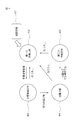
- FIG. 4 is a schematic diagram showing state transition of power transmission device 1 according to Embodiment 1 of the present invention.
- the power transmission device 1 is activated by plugging in an outlet, connecting an AC adapter, or the like (activation state 401).
- the power transmission device 1 transitions to the first standby state 402 immediately after activation.
- the control unit 102 transmits a high impedance setting instruction to the impedance switching unit 108 so that a relatively low voltage (second voltage) is supplied to the first active electrode 11a.
- the power supplied from the power supply 100 is reduced.
- the control unit 102 acquires the DC voltage value DCV detected by the I / V detector 101 and determines whether or not a resonance frequency is generated by sweeping the frequency at a constant time interval (first time interval). (Placement determination means). In a state where the power receiving device 2 is not placed, no resonance frequency is generated, so that a standby state is entered until the resonance frequency is generated, that is, until the power receiving device 2 is placed. When the control unit 102 determines that the resonance frequency is generated, the control unit 102 determines that the power receiving device 2 is placed, and transitions from the first standby state 402 to the power transmission preparation state 403.
- FIG. 5 is an exemplary diagram showing a change in the DC voltage value DCV detected by the I / V detector 101 of the power transmission device 1 according to the first embodiment of the present invention.
- the horizontal axis represents the sweep frequency
- the vertical axis represents the DC voltage value DCV and the transmission efficiency.
- a characteristic (frequency characteristic) 51 in FIG. 5 shows a change in the DC voltage value DCV when the power receiving device 2 is not mounted. As is clear from the characteristic 51, when the power receiving device 2 is not mounted, no resonance frequency is generated and no maximum value is generated in the DC voltage value DCV.
- the characteristic (frequency characteristic) 52 indicates a change in the direct-current voltage value DCV when the power receiving device 2 is mounted.
- the characteristic 52 when the power receiving device 2 is mounted, a resonance frequency is generated, and a maximum value is generated in the DC voltage value DCV.
- the transmission efficiency 53 the power transmission efficiency is highest in the vicinity of the frequency where the DC voltage value DCV becomes the maximum value, so the frequency where the DC voltage value DCV becomes the maximum value is set as the operating frequency during power transmission. By doing so, it is possible to transmit power at a frequency with the highest power transmission efficiency.
- the control unit 102 determines that the resonance frequency is generated due to a mere malfunction, or an electronic device that is not supposed to be charged is connected to the power receiving device 2. It is determined whether or not the electronic device 203 to be charged is connected to the power receiving device 2. That is, it is confirmed whether or not the placed power receiving device 2 is the power receiving device 2 to which power is transmitted (confirming means). Specifically, the determination can be made based on whether or not the frequency at which the direct-current voltage value DCV has a maximum value is within a range assumed for the electronic device 203 to be charged.
- the power receiving device to which the electronic device 203 to be charged is connected in the power transmission preparation state 403 It will be in a waiting state until 2 is mounted.
- the control unit 102 obtains the DC voltage value DCV detected by the I / V detector 101 and sweeps the frequency at regular time intervals to generate a resonance frequency. If it is determined that the resonance frequency does not occur, the electronic device that has malfunctioned, the electronic device that is not assumed to be charged, or the electronic device 203 that is the target of charging receives power.
- the frequency sampling interval during the frequency sweep is preferably set to be shorter than the frequency sampling interval in the first standby state 402. This is because it is necessary to confirm with high accuracy whether the mounted power receiving apparatus 2 is the power receiving apparatus 2 to which the electronic device 203 to be charged is connected (confirming means).
- the control unit 102 determines that the power receiving device 2 to which power is to be transmitted is placed, that is, the power receiving device 2 to which the electronic device 203 to be charged is connected is placed, the transition to the power transmission state 404 is made. Then, transmission of power to the power receiving device 2 is started. Specifically, the control unit 102 transmits a low impedance setting instruction to the impedance switching unit 108 so that a relatively high voltage (first voltage) is supplied to the first active electrode 11a. The supplied power is increased and a power transmission start instruction is transmitted to the drive control unit 103.
- the control unit 102 acquires the DC voltage value DCV detected by the I / V detector 101, and sweeps the frequency at regular time intervals to set the resonance frequency. If it is determined whether or not a resonance frequency has occurred, it is determined that the electronic device 203 or the power receiving device 2 to which the electronic device 203 is connected has been removed before charging is completed. can do. When it is determined that the resonance frequency has not occurred, it is determined that the electronic device 203 or the power receiving device 2 to which the electronic device 203 is connected has been removed before the charging is completed, and the state transitions to the first standby state 402 again.
- Whether or not charging is completed is determined based on the current value obtained by converting the AC voltage value ACV detected by the AC voltmeter 106. For example, it may be determined that charging has been completed when the current value becomes smaller than the second threshold value, or it may be determined that some abnormality has occurred when the current value becomes larger than the first threshold value. good.
- the control unit 102 determines that the charging is completed when the current value becomes smaller than the second threshold value, or that some abnormality has occurred when the current value becomes larger than the first threshold value, and the first When the state transits to the second standby state 405 and the current value is not less than the second threshold value and not more than the first threshold value, it is determined that charging is in progress.
- control unit 102 may determine whether or not charging is in progress. Even in this case, the control unit 102 acquires the AC voltage value ACV detected by the AC voltmeter 106, converts the acquired AC voltage value ACV into a current value, and monitors the converted current value. Whether or not the battery is being charged is determined, for example, based on whether or not the current value is the same value for a predetermined time. Whether or not they are the same value may be determined based on the magnitude relationship between the current value and the predetermined threshold as described above, or may be determined based on the magnitude of the fluctuation amount of the current value per unit time. For example, when judging by the magnitude of the fluctuation amount of the current value per unit time, it is judged whether or not the current value has fluctuated by a predetermined amount within the unit time. Judge that there is.
- the control unit 102 transmits a high impedance setting instruction to the impedance switching unit 108 so that a relatively low voltage (second voltage) is supplied to the first active electrode 11 a and is supplied from the power supply 100.
- a relatively low voltage second voltage
- the voltage supplied to the first active electrode 11a is not limited to the second voltage, and may be a fourth voltage lower than the first voltage.
- the control unit 102 acquires the DC voltage value DCV detected by the I / V detector 101, and determines whether a resonance frequency is generated by sweeping the frequency at a constant time interval (second time interval). To do. When it is determined that the resonance frequency is generated, the power receiving device 2 remains mounted, and thus the electronic device 203 or the power receiving device 2 to which the electronic device 203 is connected is in a waiting state. However, it is preferable to set the frequency sweep interval (second time interval) in the second standby state 405 to be longer than the frequency sweep interval (first time interval) in the first standby state 402. . This is because charging has already been completed or some abnormality has occurred, and it is not necessary to start power transmission again, and power consumption can be reduced even a little. When the control unit 102 determines that the resonance frequency has not occurred, the control unit 102 determines that the electronic device 203 or the power receiving device 2 to which the electronic device 203 is connected has been removed, and transitions to the first standby state 402 again.
- FIG. 6 is a flowchart showing a processing procedure of the control unit 102 of the power transmission device 1 according to the first embodiment of the present invention.
- the control unit 102 detects that the outlet has been plugged in, the AC adapter is connected, and the like, and activates the power transmission device 1 (step S ⁇ b> 601), and transmits a high impedance setting instruction to the impedance switching unit 108. (Step S602). Thereby, the electric power supplied from the power supply 100 can be reduced.
- the control unit 102 acquires the DC voltage value DCV detected by the I / V detector 101 (step S603), and sweeps the frequency at the first time interval to determine whether or not the maximum value exists in the DC voltage value DCV. Is determined (step S604). In the state where the power receiving device 2 is not mounted, no resonance frequency is generated, and therefore there is no maximum value in the acquired DC voltage value DCV. Therefore, whether or not the power receiving device 2 is placed can be determined according to whether or not the maximum value of the DC voltage value DCV exists.
- step S604 determines that there is no maximum value in the DC voltage value DCV (step S604: NO)
- the control unit 102 determines that the power receiving device 2 is not mounted and waits until it is mounted. It becomes a state. Specifically, the frequency characteristics of the DC voltage value DCV are analyzed by performing frequency sweeping at a constant time interval (first time interval) until the power receiving device 2 is placed.
- step S604 determines that the maximum value exists in the DC voltage value DCV (step S604: YES)
- the control unit 102 determines that the power receiving device 2 is placed on the power transmission device 1, and the DC voltage value DCV is It is determined whether or not the frequency having the maximum value is within a range assumed by the electronic device 203 to be charged (step S605).
- step S605 NO
- the control unit 102 determines that the frequency at which the DC voltage value DCV has a maximum value is not within the range assumed by the electronic device 203 to be charged (step S605: NO)
- the control unit 102 It is determined that the determination in step S604 is merely due to a malfunction or that an electronic device that is not supposed to be charged is connected, and the process returns to step S603 to repeat the above-described process.
- step S605 YES
- the control unit 102 determines that the frequency at which the direct-current voltage value DCV is a maximum value is within the range assumed by the electronic device 203 to be charged (step S605: YES)
- the control unit 102 It is determined that the power receiving device 2 to which the electronic device 203 to be charged is connected, that is, the power receiving device 2 to which power is to be transmitted is placed, and transmits a low impedance setting instruction to the impedance switching unit 108.
- Step S606 the frequency at which the DC voltage value DCV becomes the maximum value is set as the operating frequency during power transmission (Step S607). Thereby, the electric power supplied from the power supply 100 can be increased, and electric power can be transmitted at the frequency with the highest electric power transmission efficiency.
- the control unit 102 acquires the AC voltage value ACV detected by the AC voltmeter 106 (step S608), converts the acquired AC voltage value ACV into a current value, and monitors the converted current value.
- the control unit 102 determines whether or not the converted current value has changed by a predetermined amount within a predetermined time (step S609). When the control unit 102 determines that the current value has not fluctuated by a predetermined amount (step S609: NO), the control unit 102 determines that charging is in progress and enters a charging completion waiting state.
- step S609 YES
- the control unit 102 determines that the predetermined amount has changed, that is, the current value has decreased or increased by a predetermined amount within a certain time (step S609: YES)
- the control unit 102 has completed charging, or It is determined that some abnormality has occurred, and a high-impedance setting instruction is transmitted to the impedance switching unit 108 so that a relatively low voltage (second voltage) is supplied to the first active electrode 11a (step S610). .
- the electric power supplied from the power supply 100 can be reduced, and the direct-current voltage value DCV becomes small.
- the power supply circuit 12 supplies the first voltage to the first active electrode 11a and detects whether or not the power receiving device 2 is mounted. In this case, the power supply circuit 12 supplies a second voltage lower than the first voltage to the first active electrode 11a, and sweeps the frequency at a first time interval until the power receiving device 2 is mounted. When determining whether or not the charging is completed, the power supply circuit 12 supplies a second voltage lower than the first voltage to the first active electrode 11a, and the first time until the power receiving device 2 is removed. Sweep the frequency at a second time interval longer than the interval. Thereby, except when transmitting electric power, the voltage supplied to the first active electrode 11a can be lowered, and the power consumption can be reduced. Even when the power receiving device 2 is not mounted, since the voltage supplied to the first active electrode 11a is low, it is possible to avoid danger such as energization due to contact, and the safe power transmitting device 1 and It is possible to provide a power transmission control method.
- FIG. 7 is a schematic diagram illustrating state transition of the power transmission device 1 according to the second embodiment of the present invention.
- the power transmission device 1 is activated by plugging in an outlet, connecting an AC adapter, or the like (activated state 401).
- the power transmission device 1 transitions to the first standby state 402 immediately after activation.
- the control unit 102 transmits a high impedance setting instruction to the impedance switching unit 108 so that a relatively low voltage (second voltage) is supplied to the first active electrode 11a.
- the power supplied from the power supply 100 is reduced.
- the control unit 102 acquires the DC voltage value DCV detected by the I / V detector 101 and determines whether or not a resonance frequency is generated by sweeping the frequency at a constant time interval (first time interval). (Placement determination means). In a state where the power receiving device 2 is not placed, no resonance frequency is generated, so that a standby state is entered until the resonance frequency is generated, that is, until the power receiving device 2 is placed. When the control unit 102 determines that the resonance frequency is generated, the control unit 102 determines that the power receiving device 2 is placed, and transitions from the first standby state 402 to the power transmission preparation state 403.
- the control unit 102 determines whether the resonance frequency has occurred is due to a mere malfunction or whether an electronic device that is not supposed to be charged is connected to the power receiving device 2, It is determined whether or not the electronic device 203 to be charged is connected to the power receiving device 2. That is, it is confirmed whether or not the placed power receiving device 2 is the power receiving device 2 to which power is transmitted (confirming means). Specifically, the determination can be made based on whether or not the frequency at which the direct-current voltage value DCV has a maximum value is within a range assumed for the electronic device 203 to be charged.
- the control unit 102 obtains the DC voltage value DCV detected by the I / V detector 101 and sweeps the frequency at regular time intervals to generate a resonance frequency. If it is determined that the resonance frequency does not occur, the electronic device that has malfunctioned, the electronic device that is not assumed to be charged, or the electronic device 203 that is the target of charging receives power. It is determined that the device 2 has been removed or the power receiving device 2 itself has been removed, and the state transitions to the first standby state 402 again.
- the control unit 102 determines that the power receiving device 2 to which power is to be transmitted is placed, that is, the power receiving device 2 to which the electronic device 203 to be charged is connected is placed, the transition to the power transmission state 404 is made. Then, transmission of power to the power receiving device 2 is started. Specifically, the control unit 102 transmits a low impedance setting instruction to the impedance switching unit 108 so that a relatively high voltage (first voltage) is supplied to the first active electrode 11a. The supplied power is increased and a power transmission start instruction is transmitted to the drive control unit 103.
- the control unit 102 acquires the DC voltage value DCV detected by the I / V detector 101, and sweeps the frequency at regular time intervals to set the resonance frequency. If it is determined whether or not a resonance frequency has occurred, it is determined that the electronic device 203 or the power receiving device 2 to which the electronic device 203 is connected has been removed before charging is completed. can do. When it is determined that the resonance frequency has not occurred, it is determined that the electronic device 203 or the power receiving device 2 to which the electronic device 203 is connected has been removed before the charging is completed, and the state transitions to the first standby state 402 again.
- Whether or not charging is completed is determined based on the current value obtained by converting the AC voltage value ACV detected by the AC voltmeter 106. For example, it may be determined that charging has been completed when the current value becomes smaller than the second threshold value, or it may be determined that some abnormality has occurred when the current value becomes larger than the first threshold value. good.
- the control unit 102 determines that charging is completed and makes a transition to the third standby state 701, and when the current value becomes larger than the first threshold value. It is determined that some abnormality has occurred, and the state transits to the second standby state 405. If the current value is not less than the second threshold value and not more than the first threshold value, it is determined that charging is in progress.
- control unit 102 may use a determination as to whether or not charging is in progress. Even in this case, the control unit 102 acquires the AC voltage value ACV detected by the AC voltmeter 106, converts the acquired AC voltage value ACV into a current value, and monitors the converted current value. Whether or not the battery is being charged is determined, for example, based on whether or not the current value is the same value for a predetermined time. Whether or not they are the same value may be determined based on the magnitude relationship between the current value and the predetermined threshold as described above, or may be determined based on the magnitude of the fluctuation amount of the current value per unit time.
- the determination is made based on the magnitude relationship between the current value, the first threshold value, and the second threshold value as described above.
- the control unit 102 determines that some abnormality has occurred and makes a transition to the second standby state 405. In the second standby state 405, since some abnormality has occurred, it is not necessary to transmit power to the power receiving apparatus 2. Therefore, the control unit 102 transmits a high impedance setting instruction to the impedance switching unit 108 so that a relatively low voltage (second voltage) is supplied to the first active electrode 11 a and is supplied from the power supply 100. Reduce power.
- the voltage supplied to the first active electrode 11a is not limited to the second voltage, and may be a fourth voltage lower than the first voltage.
- the control unit 102 acquires the DC voltage value DCV detected by the I / V detector 101, and determines whether a resonance frequency is generated by sweeping the frequency at a constant time interval (second time interval). To do. When it is determined that the resonance frequency is generated, the power receiving device 2 remains mounted, and thus the electronic device 203 or the power receiving device 2 to which the electronic device 203 is connected is in a waiting state. However, it is preferable to set the frequency sweep interval (second time interval) in the second standby state 405 to be longer than the frequency sweep interval (first time interval) in the first standby state 402. . This is because some abnormality has occurred, or some abnormality has occurred, and it is not necessary to start power transmission again, and the power consumption can be reduced even a little. When the control unit 102 determines that the resonance frequency has not occurred, the control unit 102 determines that the electronic device 203 or the power receiving device 2 to which the electronic device 203 is connected has been removed, and transitions to the first standby state 402 again.
- the control unit 102 determines that the charging is completed and makes a transition to the third standby state 701. In the third standby state 701, since charging is completed, it is not necessary to transmit power to the power receiving device 2. Therefore, the control unit 102 transmits a high-impedance setting instruction to the impedance switching unit 108 so that a relatively low voltage (second voltage) is supplied to the second active electrode 11 a and is supplied from the power supply 100. Reduce power.
- the control unit 102 acquires the DC voltage value DCV detected by the I / V detector 101, and determines whether a resonance frequency is generated by sweeping the frequency at a constant time interval (second time interval). To do. When it is determined that the resonance frequency is generated, the power receiving device 2 remains mounted, and thus the electronic device 203 or the power receiving device 2 to which the electronic device 203 is connected is in a waiting state. However, it is preferable to set the frequency sweep interval (second time interval) in the third standby state 701 to be longer than the frequency sweep interval (first time interval) in the first standby state 402. . This is because charging has already been completed, and there is no need to start transmitting power again, so that power consumption can be reduced as much as possible. When the control unit 102 determines that the resonance frequency has not occurred, the control unit 102 determines that the electronic device 203 or the power receiving device 2 to which the electronic device 203 is connected has been removed, and transitions to the first standby state 402 again.
- control unit 102 when the control unit 102 is in a waiting state in the third standby state 701, the control unit 102 returns to the activation state 401 every predetermined time, for example, every two hours.
- the control unit 102 when there is no third standby state 701 as in the first embodiment, once charging is completed, charging is not started again, and when the power receiving device 2 is left standing, spontaneous discharge occurs. As a result, the power receiving device 2 may not be usable.
- the third standby state 701 it is possible to return to the activated state 401 when a predetermined time has elapsed, so that the power receiving device 2 remains mounted and is removed from the power transmitting device 1. Even if the user forgets that, the state of charge can be maintained.
- FIG. 8 is a flowchart showing a processing procedure of the control unit 102 of the power transmission device 1 according to the second embodiment of the present invention.
- the processing from step S601 to step S608 is the same as that in the first embodiment, and thus detailed description thereof is omitted.
- the control unit 102 of the power transmission device 1 acquires the AC voltage value ACV detected by the AC voltmeter 106 (step S608), converts the acquired AC voltage value ACV into a current value, and monitors the converted current value.
- the control unit 102 determines whether or not the converted current value is larger than the first threshold value (step S801).
- step S801 determines that the current value is greater than the first threshold value (step S801: YES)
- the control unit 102 determines that some abnormality has occurred during charging and determines a relatively low voltage (second Is transmitted to the impedance switching unit 108 so that the first active electrode 11a is supplied to the first active electrode 11a (step S802). Thereby, the electric power supplied from the power supply 100 can be reduced.
- the control unit 102 returns the process to step S603 and repeats the above-described process.
- step S803 determines whether the current value is smaller than the second threshold value (step S803).
- step S803: NO determines that the current value is greater than or equal to the second threshold value
- step S803: NO determines that charging is not completed, and returns the process to step S801 to perform the above-described process.
- step S803: YES determines that the charging is completed, and a relatively low voltage (second voltage) is obtained.
- a high impedance setting instruction is transmitted to the impedance switching unit 108 so as to be supplied to the first active electrode 11a (step S804). Thereby, the electric power supplied from the power supply 100 can be reduced.
- the control unit 102 determines whether or not a predetermined time has elapsed (step S805). When the control unit 102 determines that the predetermined time has not elapsed (step S805: NO), the control unit 102 determines that the charged electric power still remains and enters a waiting state. When the control unit 102 determines that the predetermined time has elapsed (step S805: YES), the control unit 102 determines that the charged power has already been discharged, returns the process to step S601, and described above. Repeat the process.
- the second standby state 405 when it is determined that some abnormality has occurred in the power transmission state 404, the second standby state 405 is entered, and when it is determined that charging is completed, the third standby state is established.
- the state transitions to the state 701, and in the third standby state 701, the state is returned to the activated state 401 when a predetermined time has elapsed, so the power receiving device 2 in a state where charging has been completed is left on the power transmitting device 1 Even in this case, the state of charge can be maintained.
- FIG. 9 is a flowchart illustrating a processing procedure of the control unit 102 of the power transmission device 1 according to the third embodiment of the present invention.
- the processes in steps S601 and S602 are the same as those in the first embodiment, and thus detailed description thereof is omitted.
- the high impedance value instructed in step S602 is higher than those in the first and second embodiments, that is, it is preferable to further reduce the power supplied from the power supply 100.
- the control unit 102 transmits a high impedance setting instruction to the impedance switching unit 108 (step S602). Thereby, the electric power supplied from the power supply 100 can be reduced.
- the DC voltage value DCV supplied from the power supply circuit 12 is set to a high impedance value that is instructed to be set to be smaller than the DC voltage value DCV in the first standby state 402 that transitions immediately after the power transmission device 1 is started. Make it high. Accordingly, the third voltage lower than the second voltage in the case where it is determined whether or not the power receiving device 2 is placed in the first standby state 402 on the first active electrode 11a of the power transmitting device 1. Supply. This is because it is sufficient to supply power necessary for data communication.
- the control unit 102 acquires the DC voltage value DCV detected by the I / V detector 101 (step S603), and sweeps the frequency at the first time interval to determine whether or not the maximum value exists in the DC voltage value DCV. Is determined (step S604). In a state where the power receiving device 2 is not mounted, no resonance frequency is generated, and therefore there is no maximum value in the acquired DC voltage value DCV. Therefore, whether or not the power receiving device 2 is placed can be determined according to whether or not the maximum value of the DC voltage value DCV exists.
- step S604 determines that there is no maximum value in the DC voltage value DCV (step S604: NO)
- the control unit 102 determines that the power receiving device 2 is not mounted and waits until it is mounted. It becomes a state. Specifically, the frequency characteristics of the DC voltage value DCV are analyzed by performing frequency sweeping at a constant time interval (first time interval) until the power receiving device 2 is placed.
- step S604 determines that there is a maximum value in the DC voltage value DCV (step S604: YES)
- the control unit 102 determines that the power receiving device 2 is placed on the power transmission device 1, and places the received power.
- a communication frequency for communicating with the device 2 is set (step S901).
- the control unit 102 determines whether or not data communication with the power receiving apparatus 2 is possible (step S902). When the control unit 102 determines that data communication is not possible (step S902: NO), the control unit 102 is placed. It is determined that it is not the power receiving device 2 that is the target for transmitting power, and the processing is terminated. When the control unit 102 determines that data communication is possible (step S902: YES), the control unit 102 acquires the identification ID of the power receiving device 2 (step S903).
- control unit 102 can acquire the identification ID
- the control unit 102 can confirm that the power receiving device 2 to which power is to be transmitted is placed. Therefore, the power receiving device 2 and data corresponding to the acquired identification ID can be confirmed.
- Communication is performed to acquire parameters necessary for power reception for each power receiving device 2 (step S904), and an operating frequency at the time of power transmission is specified and set based on the acquired parameters (step S905). Is transmitted (step S906).
- a data communication method for acquiring parameters necessary for power reception for each power receiving device 2 is not particularly limited, and for example, data communication may be performed by a load modulation method. Even in this case, the operating frequency during power transmission can be specified based on the acquired parameters.
- the power transmission device 1 and the power reception device 2 perform data communication and acquire an identification ID for identifying the power reception device 2, so that the power reception device to which power is transmitted is obtained. It can be determined that 2 is placed.
- the power transmission device 1 and the power reception device 2 since it is possible to recognize which type of power receiving device 2 is mounted based on parameters necessary for power reception for each power receiving device 2, it is possible to appropriately specify the operating frequency during power transmission. Therefore, it is possible to transmit power efficiently.
Abstract
Description
図1は、本発明の実施の形態1に係る送電装置の構成を模式的に示す回路図である。図1(a)に示すように、本実施の形態1に係る送電装置1は、少なくとも高周波発生回路(電源回路)12と、昇圧トランス13と、第一の能動電極11a及び第一の受動電極11pで構成された第一の結合電極11とを備えている。図1(a)の回路では、昇圧トランス13により昇圧されると、第一の能動電極11aは高電圧となり、第一の受動電極11pは低電圧となる。
本発明の実施の形態2に係る送電装置を用いた電力伝送システムの構成は、実施の形態1と同様であることから、同一の符号を付することで詳細な説明は省略する。本実施の形態2では、送電状態404で何らかの異常が発生したと判定した場合には第二の待機状態405へ、充電が完了したと判定した場合には新たな第三の待機状態へ、それぞれ状態遷移する点で実施の形態1とは相違する。
本発明の実施の形態3に係る送電装置を用いた電力伝送システムの構成は、実施の形態1及び2と同様であることから、同一の符号を付することで詳細な説明は省略する。本実施の形態3では、送電装置1と受電装置2とが通信することにより、受電装置2に適した動作周波数にて電力伝送する点で実施の形態1及び2とは相違する。
2 受電装置
11a 第一の能動電極
11p 第一の受動電極
12 高周波発生回路(電源回路)
21a 第二の能動電極
21p 第二の受動電極
100 電源
102 制御部
Claims (14)
- 第一の受動電極と第一の能動電極とを有し、
前記第一の能動電極と受電装置の第二の能動電極とを間隙を介して対向させ、前記第一の受動電極と前記受電装置の第二の受動電極とを対向させて容量結合させ、
前記第一の能動電極と前記第二の能動電極との間に、前記第一の受動電極と前記第二の受動電極との間よりも強い電場を形成することにより非接触で電力を伝送する送電装置において、
電力を供給する電源回路と、
前記受電装置が載置されているか否かを検知する受電装置検知手段と、
前記受電装置の充電状態を監視する充電状態監視手段と、
充電状態に応じて前記電源回路の出力を制御する送電制御手段と
を備え、
前記送電制御手段は、以下に示すように前記電源回路の出力を制御することを特徴とする送電装置。
(1)電力伝送時、前記電源回路に、第一の電圧を前記第一の能動電極へ供給させる。
(2)前記電源回路に、前記第一の電圧より低い第二の電圧を前記第一の能動電極へ供給させ、前記受電装置検知手段に、前記受電装置が載置されるまで第一の時間間隔で周波数掃引させる。
(3)前記電源回路に、前記第一の電圧より低い第四の電圧を前記第一の能動電極へ供給させ、前記受電装置検知手段に、前記受電装置が取り外されるまで前記第一の時間間隔より長い第二の時間間隔で周波数掃引させる。 - 前記受電装置検知手段は、所定の周波数範囲で周波数掃引することにより電圧の周波数特性を測定し、電圧値が極大値となる周波数を検出した場合に前記受電装置が載置されたと判定する載置判定手段を備えることを特徴とする請求項1に記載の送電装置。
- 前記充電状態監視手段は、前記第一の受動電極と前記第一の能動電極とに出力する電流値を監視しており、
前記電流値に基づいて、充電が完了したか否かを判定する判定手段を備えることを特徴とする請求項1又は2に記載の送電装置。 - 前記受電装置検知手段で前記受電装置が載置されていると検知した場合、該受電装置が電力を伝送する対象となる受電装置であるか否かを確認する確認手段を備え、
前記送電制御手段は、前記確認手段での確認結果が出るまで、周波数掃引時の周波数サンプリング間隔を、前記受電装置が載置されているか否かを判定するための周波数掃引時の周波数サンプリング間隔よりも短くなるよう設定することを特徴とする請求項1乃至3のいずれか一項に記載の送電装置。 - 前記送電制御手段は、前記電源回路に、前記第二の電圧より低い第三の電圧を前記第一の能動電極へ供給させ、
前記確認手段は、前記受電装置とデータ通信することにより前記受電装置を識別する識別情報を取得した場合に、前記受電装置が電力を伝送する対象であると確認することを特徴とする請求項4に記載の送電装置。 - 前記充電状態監視手段は、前記電流値と第一の閾値及び該第一の閾値より小さい第二の閾値との大小関係を監視しており、前記判定手段は、前記電流値が前記第一の閾値より大きいと判断した場合には異常が発生したと、前記第二の閾値より小さいと判断した場合には充電が完了したと判定することを特徴とする請求項3乃至5のいずれか一項に記載の送電装置。
- 前記送電制御手段は、
前記受電装置と負荷変調方式によりデータ通信して、前記受電装置ごとの受電に必要なパラメータを取得し、
取得したパラメータに基づいて電力伝送時の周波数を特定することを特徴とする請求項1乃至5のいずれか一項に記載の送電装置。 - 第一の受動電極と第一の能動電極とを有する送電装置と、
第二の受動電極と第二の能動電極とを有する受電装置と
を用い、
前記第一の能動電極と前記第二の能動電極とを間隙を介して対向させ、前記第一の受動電極と前記第二の受動電極とを対向させて容量結合させ、前記第一の能動電極と前記第二の能動電極との間に、前記第一の受動電極と前記第二の受動電極との間よりも強い電場を形成することにより非接触で電力を伝送する送電制御方法において、
前記送電装置は、
前記受電装置が載置されているか否かを検知し、
前記受電装置の充電状態を監視し、
充電状態に応じて電力を供給する電源回路の出力を以下のように制御することを特徴とする送電制御方法。
(1)電力伝送時、前記電源回路は、第一の電圧を前記第一の能動電極へ供給する。
(2)前記電源回路は、前記第一の電圧より低い第二の電圧を前記第一の能動電極へ供給し、前記送電装置は前記受電装置が載置されるまで第一の時間間隔で周波数掃引する。
(3)前記電源回路は、前記第一の電圧より低い第四の電圧を前記第一の能動電極へ供給し、前記送電装置は前記受電装置が取り外されるまで前記第一の時間間隔より長い第二の時間間隔で周波数掃引する。 - 前記送電装置は、所定の周波数範囲で周波数掃引することにより電圧の周波数特性を測定し、電圧値が極大値となる周波数を検出した場合に前記受電装置が載置されたと判定することを特徴とする請求項8に記載の送電制御方法。
- 前記送電装置は、前記第一の受動電極と前記第一の能動電極とに出力する電流値を監視し、
前記電流値に基づいて、充電が完了したか否かを判定することを特徴とする請求項8又は9に記載の送電制御方法。 - 前記送電装置は、前記受電装置が載置されていると検知した場合、該受電装置が電力を伝送する対象となる受電装置であるか否かを確認し、
確認結果が出るまで、周波数掃引時の周波数サンプリング間隔を、前記受電装置が載置されているか否かを判定するための周波数掃引時の周波数サンプリング間隔よりも短くなるよう設定することを特徴とする請求項8乃至10のいずれか一項に記載の送電制御方法。 - 前記電源回路は、前記第二の電圧より低い第三の電圧を前記第一の能動電極へ供給し、
前記送電装置は、前記受電装置とデータ通信することにより前記受電装置を識別する識別情報を取得した場合に、前記受電装置が電力を伝送する対象であると確認することを特徴とする請求項11に記載の送電制御方法。 - 前記送電装置は、前記電流値と第一の閾値及び該第一の閾値より小さい第二の閾値との大小関係を監視し、前記電流値が前記第一の閾値より大きいと判断した場合には異常が発生したと、前記第二の閾値より小さいと判断した場合には充電が完了したと判定することを特徴とする請求項10乃至12のいずれか一項に記載の送電制御方法。
- 前記送電装置が、前記受電装置と負荷変調方式によりデータ通信して、前記受電装置ごとの受電に必要なパラメータを取得し、
取得したパラメータに基づいて電力伝送時の周波数を特定することを特徴とする請求項8乃至12のいずれか一項に記載の送電制御方法。
Priority Applications (4)
| Application Number | Priority Date | Filing Date | Title |
|---|---|---|---|
| JP2013545836A JP5541422B2 (ja) | 2011-11-24 | 2012-10-01 | 送電装置及び送電制御方法 |
| CN201280057227.9A CN103947080B (zh) | 2011-11-24 | 2012-10-01 | 供电装置以及供电控制方法 |
| GB1408917.1A GB2511448B (en) | 2011-11-24 | 2012-10-01 | Power transmission device and power transmission control method |
| US14/282,566 US9735589B2 (en) | 2011-11-24 | 2014-05-20 | Power transmission device and power transmission control method |
Applications Claiming Priority (2)
| Application Number | Priority Date | Filing Date | Title |
|---|---|---|---|
| JP2011256808 | 2011-11-24 | ||
| JP2011-256808 | 2011-11-24 |
Related Child Applications (1)
| Application Number | Title | Priority Date | Filing Date |
|---|---|---|---|
| US14/282,566 Continuation US9735589B2 (en) | 2011-11-24 | 2014-05-20 | Power transmission device and power transmission control method |
Publications (1)
| Publication Number | Publication Date |
|---|---|
| WO2013077086A1 true WO2013077086A1 (ja) | 2013-05-30 |
Family
ID=48469542
Family Applications (1)
| Application Number | Title | Priority Date | Filing Date |
|---|---|---|---|
| PCT/JP2012/075364 WO2013077086A1 (ja) | 2011-11-24 | 2012-10-01 | 送電装置及び送電制御方法 |
Country Status (5)
| Country | Link |
|---|---|
| US (1) | US9735589B2 (ja) |
| JP (2) | JP5541422B2 (ja) |
| CN (2) | CN103947080B (ja) |
| GB (1) | GB2511448B (ja) |
| WO (1) | WO2013077086A1 (ja) |
Cited By (5)
| Publication number | Priority date | Publication date | Assignee | Title |
|---|---|---|---|---|
| WO2014196384A1 (ja) * | 2013-06-06 | 2014-12-11 | 株式会社村田製作所 | 非接触電力伝送システムの検査装置及び検査方法 |
| WO2015037525A1 (ja) * | 2013-09-12 | 2015-03-19 | 株式会社村田製作所 | 送電装置及びワイヤレス電力伝送システム |
| WO2015037526A1 (ja) * | 2013-09-12 | 2015-03-19 | 株式会社村田製作所 | 送電装置及びワイヤレス電力伝送システム |
| WO2015037861A1 (en) | 2013-09-13 | 2015-03-19 | Samsung Electronics Co., Ltd. | Method of power transmitting unit (ptu) for determining location of power receiving unit (pru), and ptu employing the method |
| WO2019117140A1 (ja) * | 2017-12-11 | 2019-06-20 | パナソニックIpマネジメント株式会社 | 無線電力伝送システム、送電装置、および受電装置 |
Families Citing this family (8)
| Publication number | Priority date | Publication date | Assignee | Title |
|---|---|---|---|---|
| JP5541422B2 (ja) * | 2011-11-24 | 2014-07-09 | 株式会社村田製作所 | 送電装置及び送電制御方法 |
| JP5899306B2 (ja) * | 2012-03-14 | 2016-04-06 | パイオニア株式会社 | 非接触充電システム、非接触送電装置及び方法、並びに非接触受電装置及び方法 |
| KR101943082B1 (ko) * | 2014-01-23 | 2019-04-18 | 한국전자통신연구원 | 무선 전력 송신 장치, 무선 전력 수신 장치, 및 무선 전력 전송 시스템 |
| JP6665568B2 (ja) * | 2016-02-12 | 2020-03-13 | セイコーエプソン株式会社 | 制御装置、受電装置、電子機器、電力伝送システム及び電力供給方法 |
| US10879704B2 (en) | 2016-08-26 | 2020-12-29 | Nucurrent, Inc. | Wireless connector receiver module |
| US10530177B2 (en) * | 2017-03-09 | 2020-01-07 | Cochlear Limited | Multi-loop implant charger |
| CN111279577B (zh) * | 2017-11-07 | 2023-10-17 | 内盖夫本古里安大学技术与应用有限公司 | 借助于自适应匹配网络的电容性无线电力传输 |
| US11171517B2 (en) | 2018-03-28 | 2021-11-09 | Panasonic Intellectual Property Management Co., Ltd. | Electrode unit, power transmitting device, power receiving device, and wireless power transmission system |
Citations (4)
| Publication number | Priority date | Publication date | Assignee | Title |
|---|---|---|---|---|
| JPH06150079A (ja) * | 1992-11-13 | 1994-05-31 | Pfu Ltd | 非接触型icメモリカードシステム |
| JPH08214405A (ja) * | 1995-02-02 | 1996-08-20 | Technova:Kk | 非接触送電装置 |
| JP2006230129A (ja) * | 2005-02-18 | 2006-08-31 | Nanao Corp | 非接触電力供給装置 |
| JP2010193692A (ja) * | 2009-02-20 | 2010-09-02 | Takenaka Komuten Co Ltd | 電力供給システム |
Family Cites Families (17)
| Publication number | Priority date | Publication date | Assignee | Title |
|---|---|---|---|---|
| US7356952B2 (en) * | 2002-06-17 | 2008-04-15 | Philip Morris Usa Inc. | System for coupling package displays to remote power source |
| US7570994B2 (en) * | 2003-04-25 | 2009-08-04 | Medtronic Physio-Control Corp. | Apparatus and method for maintaining a defibrillator battery charge and optionally communicating |
| JP2006060909A (ja) * | 2004-08-19 | 2006-03-02 | Seiko Epson Corp | 非接触電力伝送装置 |
| CN100549880C (zh) * | 2004-11-02 | 2009-10-14 | 光宝科技股份有限公司 | 节能电路 |
| BRPI0621437A2 (pt) | 2006-03-21 | 2012-07-10 | Tmms Co Ltd | dispositivos de transporte da eletricidade através do vácuo e de materiais dielétricos |
| US7989986B2 (en) * | 2006-03-23 | 2011-08-02 | Access Business Group International Llc | Inductive power supply with device identification |
| JP4494426B2 (ja) * | 2007-02-16 | 2010-06-30 | セイコーエプソン株式会社 | 送電制御装置、受電制御装置、無接点電力伝送システム、送電装置、受電装置および電子機器 |
| JP2008236968A (ja) * | 2007-03-23 | 2008-10-02 | Seiko Epson Corp | 非接触電力伝送装置 |
| FR2920061A1 (fr) * | 2007-08-17 | 2009-02-20 | Patrick Camurati | Procede et dispositif de transport, distribution et gestion de l'energie electrique par couplage longitudinal a distance en champ proche entre dipoles electriques |
| JP5473356B2 (ja) * | 2008-02-28 | 2014-04-16 | シチズンホールディングス株式会社 | 表示パネル及び表示パネルの製造方法 |
| JP2009273327A (ja) * | 2008-05-10 | 2009-11-19 | Sanyo Electric Co Ltd | 電池内蔵機器と充電台 |
| JP4725664B2 (ja) | 2008-06-25 | 2011-07-13 | セイコーエプソン株式会社 | 送電制御装置、送電装置、受電制御装置、受電装置、電子機器、送電制御方法、及び受電制御方法 |
| JP2010028934A (ja) * | 2008-07-16 | 2010-02-04 | Seiko Epson Corp | 受電制御装置、受電装置および無接点電力伝送システム |
| JP5417907B2 (ja) | 2009-03-09 | 2014-02-19 | セイコーエプソン株式会社 | 送電制御装置、送電装置、受電制御装置、受電装置、電子機器および無接点電力伝送システム |
| JP5689587B2 (ja) * | 2009-03-31 | 2015-03-25 | 富士通株式会社 | 電力伝送装置 |
| US9496743B2 (en) * | 2010-09-13 | 2016-11-15 | Semiconductor Energy Laboratory Co., Ltd. | Power receiving device and wireless power feed system |
| JP5541422B2 (ja) * | 2011-11-24 | 2014-07-09 | 株式会社村田製作所 | 送電装置及び送電制御方法 |
-
2012
- 2012-10-01 JP JP2013545836A patent/JP5541422B2/ja active Active
- 2012-10-01 CN CN201280057227.9A patent/CN103947080B/zh active Active
- 2012-10-01 WO PCT/JP2012/075364 patent/WO2013077086A1/ja active Application Filing
- 2012-10-01 GB GB1408917.1A patent/GB2511448B/en active Active
- 2012-10-01 CN CN201610237040.7A patent/CN105720613B/zh active Active
-
2014
- 2014-04-24 JP JP2014090030A patent/JP5776815B2/ja active Active
- 2014-05-20 US US14/282,566 patent/US9735589B2/en active Active
Patent Citations (4)
| Publication number | Priority date | Publication date | Assignee | Title |
|---|---|---|---|---|
| JPH06150079A (ja) * | 1992-11-13 | 1994-05-31 | Pfu Ltd | 非接触型icメモリカードシステム |
| JPH08214405A (ja) * | 1995-02-02 | 1996-08-20 | Technova:Kk | 非接触送電装置 |
| JP2006230129A (ja) * | 2005-02-18 | 2006-08-31 | Nanao Corp | 非接触電力供給装置 |
| JP2010193692A (ja) * | 2009-02-20 | 2010-09-02 | Takenaka Komuten Co Ltd | 電力供給システム |
Cited By (17)
| Publication number | Priority date | Publication date | Assignee | Title |
|---|---|---|---|---|
| US10191119B2 (en) | 2013-06-06 | 2019-01-29 | Murata Manufacturing Co., Ltd. | Inspecting apparatus and inspecting method for noncontact power transfer system |
| WO2014196384A1 (ja) * | 2013-06-06 | 2014-12-11 | 株式会社村田製作所 | 非接触電力伝送システムの検査装置及び検査方法 |
| JP5794407B2 (ja) * | 2013-06-06 | 2015-10-14 | 株式会社村田製作所 | 非接触電力伝送システムの検査装置及び検査方法 |
| CN105190327A (zh) * | 2013-06-06 | 2015-12-23 | 株式会社村田制作所 | 非接触电力输送系统的检查装置及检查方法 |
| US9866040B2 (en) | 2013-09-12 | 2018-01-09 | Murata Manufacturing Co., Ltd. | Power transmission device and wireless power transmission system |
| WO2015037525A1 (ja) * | 2013-09-12 | 2015-03-19 | 株式会社村田製作所 | 送電装置及びワイヤレス電力伝送システム |
| WO2015037526A1 (ja) * | 2013-09-12 | 2015-03-19 | 株式会社村田製作所 | 送電装置及びワイヤレス電力伝送システム |
| JP5861808B2 (ja) * | 2013-09-12 | 2016-02-16 | 株式会社村田製作所 | 送電装置及びワイヤレス電力伝送システム |
| JP5900709B2 (ja) * | 2013-09-12 | 2016-04-06 | 株式会社村田製作所 | 送電装置及びワイヤレス電力伝送システム |
| KR20150031357A (ko) * | 2013-09-13 | 2015-03-24 | 삼성전자주식회사 | 전력 전송 장치에서 전력 수신 장치의 위치를 판단하는 방법 및 상기 방법을 수행하는 전력 전송 장치 |
| EP3047558A4 (en) * | 2013-09-13 | 2017-05-17 | Samsung Electronics Co., Ltd. | Method of power transmitting unit (ptu) for determining location of power receiving unit (pru), and ptu employing the method |
| EP3047558A1 (en) * | 2013-09-13 | 2016-07-27 | Samsung Electronics Co., Ltd. | Method of power transmitting unit (ptu) for determining location of power receiving unit (pru), and ptu employing the method |
| US9985458B2 (en) | 2013-09-13 | 2018-05-29 | Samsung Electronics Co., Ltd. | Method of power transmitting unit (PTU) for determining location of power receiving unit (PRU), and PTU employing the method |
| WO2015037861A1 (en) | 2013-09-13 | 2015-03-19 | Samsung Electronics Co., Ltd. | Method of power transmitting unit (ptu) for determining location of power receiving unit (pru), and ptu employing the method |
| KR102109764B1 (ko) * | 2013-09-13 | 2020-05-29 | 삼성전자주식회사 | 전력 전송 장치에서 전력 수신 장치의 위치를 판단하는 방법 및 상기 방법을 수행하는 전력 전송 장치 |
| WO2019117140A1 (ja) * | 2017-12-11 | 2019-06-20 | パナソニックIpマネジメント株式会社 | 無線電力伝送システム、送電装置、および受電装置 |
| US11159048B2 (en) | 2017-12-11 | 2021-10-26 | Panasonic Intellectual Property Management Co., Ltd. | Wireless power transmission system, power transmitting device, and power receiving device with circuit to apply a trigger signal |
Also Published As
| Publication number | Publication date |
|---|---|
| CN103947080A (zh) | 2014-07-23 |
| GB201408917D0 (en) | 2014-07-02 |
| GB2511448A (en) | 2014-09-03 |
| JP5776815B2 (ja) | 2015-09-09 |
| US9735589B2 (en) | 2017-08-15 |
| GB2511448B (en) | 2017-10-04 |
| JP2014168377A (ja) | 2014-09-11 |
| CN105720613A (zh) | 2016-06-29 |
| US20140253052A1 (en) | 2014-09-11 |
| CN103947080B (zh) | 2016-05-11 |
| JPWO2013077086A1 (ja) | 2015-04-27 |
| CN105720613B (zh) | 2018-07-27 |
| JP5541422B2 (ja) | 2014-07-09 |
Similar Documents
| Publication | Publication Date | Title |
|---|---|---|
| JP5776815B2 (ja) | 送電装置及び送電制御方法 | |
| US8987941B2 (en) | Power transmission system | |
| EP3185262B1 (en) | Wireless power transfer method, apparatus and system | |
| US9246358B2 (en) | Wireless power transmitting apparatus having signal detecting circuit for detecting transmission signals | |
| KR102004541B1 (ko) | 공진형 무선 전력 전송 시스템에서의 무선 전력 전송 제어 방법, 이를 이용하는 무선 전력 전송 장치, 및 이를 이용하는 무선 전력 수신 장치 | |
| US9006937B2 (en) | System and method for enabling ongoing inductive power transmission | |
| EP2615718B1 (en) | Over-voltage protection device for resonant wireless power reception device and method for controlling the over-voltage protection device | |
| CN101253591B (zh) | 用于ac-ac电源的负载检测器 | |
| EP3306781A1 (en) | Wireless power transmission system and method for driving same | |
| US20130187479A1 (en) | Electric power transmission system and power transmission device used in the electric power transmission system | |
| JP6279452B2 (ja) | 非接触電力伝送装置 | |
| JP5516824B2 (ja) | 電力伝送システム | |
| JP5839105B2 (ja) | 送電装置及び送電制御方法 | |
| CN108574343B (zh) | 非接触式电力传输装置及非接触式送电装置 | |
| JP2013070581A (ja) | 共鳴型ワイヤレス充電装置 | |
| KR20150056222A (ko) | 동시 멀티 충전이 가능한 무선 전력 전송 장치 | |
| KR20100112034A (ko) | 무접점 충전제어장치 및 충전제어방법 | |
| JP6061019B2 (ja) | 送電装置およびワイヤレス電力伝送システム | |
| KR20170082281A (ko) | 무선 전력 전송 시스템에서 무선 전력 송신기 및 수신기 | |
| US20150333558A1 (en) | Wireless charger units for powering low-cost disposable electronic systems and related methods |
Legal Events
| Date | Code | Title | Description |
|---|---|---|---|
| WWE | Wipo information: entry into national phase |
Ref document number: 201280057227.9 Country of ref document: CN |
|
| 121 | Ep: the epo has been informed by wipo that ep was designated in this application |
Ref document number: 12852142 Country of ref document: EP Kind code of ref document: A1 |
|
| ENP | Entry into the national phase |
Ref document number: 2013545836 Country of ref document: JP Kind code of ref document: A |
|
| ENP | Entry into the national phase |
Ref document number: 1408917 Country of ref document: GB Kind code of ref document: A Free format text: PCT FILING DATE = 20121001 |
|
| WWE | Wipo information: entry into national phase |
Ref document number: 1408917.1 Country of ref document: GB |
|
| NENP | Non-entry into the national phase |
Ref country code: DE |
|
| 122 | Ep: pct application non-entry in european phase |
Ref document number: 12852142 Country of ref document: EP Kind code of ref document: A1 |