WO2013073702A1 - 複合icカード - Google Patents
複合icカード Download PDFInfo
- Publication number
- WO2013073702A1 WO2013073702A1 PCT/JP2012/079992 JP2012079992W WO2013073702A1 WO 2013073702 A1 WO2013073702 A1 WO 2013073702A1 JP 2012079992 W JP2012079992 W JP 2012079992W WO 2013073702 A1 WO2013073702 A1 WO 2013073702A1
- Authority
- WO
- WIPO (PCT)
- Prior art keywords
- coil
- card
- composite
- antenna
- coupling coil
- Prior art date
Links
Images


Classifications
-
- G—PHYSICS
- G06—COMPUTING; CALCULATING OR COUNTING
- G06K—GRAPHICAL DATA READING; PRESENTATION OF DATA; RECORD CARRIERS; HANDLING RECORD CARRIERS
- G06K19/00—Record carriers for use with machines and with at least a part designed to carry digital markings
- G06K19/06—Record carriers for use with machines and with at least a part designed to carry digital markings characterised by the kind of the digital marking, e.g. shape, nature, code
- G06K19/067—Record carriers with conductive marks, printed circuits or semiconductor circuit elements, e.g. credit or identity cards also with resonating or responding marks without active components
- G06K19/07—Record carriers with conductive marks, printed circuits or semiconductor circuit elements, e.g. credit or identity cards also with resonating or responding marks without active components with integrated circuit chips
- G06K19/077—Constructional details, e.g. mounting of circuits in the carrier
- G06K19/07749—Constructional details, e.g. mounting of circuits in the carrier the record carrier being capable of non-contact communication, e.g. constructional details of the antenna of a non-contact smart card
- G06K19/07773—Antenna details
- G06K19/07777—Antenna details the antenna being of the inductive type
- G06K19/07779—Antenna details the antenna being of the inductive type the inductive antenna being a coil
- G06K19/07783—Antenna details the antenna being of the inductive type the inductive antenna being a coil the coil being planar
-
- G—PHYSICS
- G06—COMPUTING; CALCULATING OR COUNTING
- G06K—GRAPHICAL DATA READING; PRESENTATION OF DATA; RECORD CARRIERS; HANDLING RECORD CARRIERS
- G06K19/00—Record carriers for use with machines and with at least a part designed to carry digital markings
- G06K19/06—Record carriers for use with machines and with at least a part designed to carry digital markings characterised by the kind of the digital marking, e.g. shape, nature, code
- G06K19/067—Record carriers with conductive marks, printed circuits or semiconductor circuit elements, e.g. credit or identity cards also with resonating or responding marks without active components
- G06K19/07—Record carriers with conductive marks, printed circuits or semiconductor circuit elements, e.g. credit or identity cards also with resonating or responding marks without active components with integrated circuit chips
- G06K19/077—Constructional details, e.g. mounting of circuits in the carrier
- G06K19/07749—Constructional details, e.g. mounting of circuits in the carrier the record carrier being capable of non-contact communication, e.g. constructional details of the antenna of a non-contact smart card
- G06K19/07766—Constructional details, e.g. mounting of circuits in the carrier the record carrier being capable of non-contact communication, e.g. constructional details of the antenna of a non-contact smart card comprising at least a second communication arrangement in addition to a first non-contact communication arrangement
- G06K19/07769—Constructional details, e.g. mounting of circuits in the carrier the record carrier being capable of non-contact communication, e.g. constructional details of the antenna of a non-contact smart card comprising at least a second communication arrangement in addition to a first non-contact communication arrangement the further communication means being a galvanic interface, e.g. hybrid or mixed smart cards having a contact and a non-contact interface
-
- G—PHYSICS
- G06—COMPUTING; CALCULATING OR COUNTING
- G06K—GRAPHICAL DATA READING; PRESENTATION OF DATA; RECORD CARRIERS; HANDLING RECORD CARRIERS
- G06K19/00—Record carriers for use with machines and with at least a part designed to carry digital markings
- G06K19/06—Record carriers for use with machines and with at least a part designed to carry digital markings characterised by the kind of the digital marking, e.g. shape, nature, code
- G06K19/067—Record carriers with conductive marks, printed circuits or semiconductor circuit elements, e.g. credit or identity cards also with resonating or responding marks without active components
- G06K19/07—Record carriers with conductive marks, printed circuits or semiconductor circuit elements, e.g. credit or identity cards also with resonating or responding marks without active components with integrated circuit chips
- G06K19/077—Constructional details, e.g. mounting of circuits in the carrier
- G06K19/07749—Constructional details, e.g. mounting of circuits in the carrier the record carrier being capable of non-contact communication, e.g. constructional details of the antenna of a non-contact smart card
- G06K19/07773—Antenna details
- G06K19/07794—Antenna details the record carrier comprising a booster or auxiliary antenna in addition to the antenna connected directly to the integrated circuit
-
- H—ELECTRICITY
- H01—ELECTRIC ELEMENTS
- H01Q—ANTENNAS, i.e. RADIO AERIALS
- H01Q1/00—Details of, or arrangements associated with, antennas
- H01Q1/12—Supports; Mounting means
- H01Q1/22—Supports; Mounting means by structural association with other equipment or articles
- H01Q1/2208—Supports; Mounting means by structural association with other equipment or articles associated with components used in interrogation type services, i.e. in systems for information exchange between an interrogator/reader and a tag/transponder, e.g. in Radio Frequency Identification [RFID] systems
- H01Q1/2225—Supports; Mounting means by structural association with other equipment or articles associated with components used in interrogation type services, i.e. in systems for information exchange between an interrogator/reader and a tag/transponder, e.g. in Radio Frequency Identification [RFID] systems used in active tags, i.e. provided with its own power source or in passive tags, i.e. deriving power from RF signal
-
- H—ELECTRICITY
- H01—ELECTRIC ELEMENTS
- H01Q—ANTENNAS, i.e. RADIO AERIALS
- H01Q1/00—Details of, or arrangements associated with, antennas
- H01Q1/40—Radiating elements coated with or embedded in protective material
-
- H—ELECTRICITY
- H01—ELECTRIC ELEMENTS
- H01Q—ANTENNAS, i.e. RADIO AERIALS
- H01Q7/00—Loop antennas with a substantially uniform current distribution around the loop and having a directional radiation pattern in a plane perpendicular to the plane of the loop
Definitions
- the present invention is a contact type that receives power supply power, exchanges signals via electrical contacts, etc., and power supply power reception, signal exchanges, etc., without contact by an electromagnetic coupling method without providing electrical contacts on an IC card.
- the present invention relates to a composite IC card functioning as both a non-contact type performed in the above and a manufacturing method thereof.
- a so-called composite IC card that functions both as a contact type and a non-contact type is known.
- an antenna coil provided in the card for non-contact communication with an external terminal and an IC module functioning as both a contact type and a non-contact type are physically connected by wiring.
- a compound IC card is formed on an IC module that functions as both a contact type and a non-contact type, and the coil for non-contact electrical connection with the coil formed on the IC module is in non-contact communication with an external terminal.
- a composite IC card in which an antenna coil is provided in the card (see Patent Documents 1, 2, and 3).
- the latter composite IC card does not need to physically connect the IC module and the antenna coil by wiring, and is not likely to cause poor contact or the like.
- a card base having an antenna coil and a coil for electrically connecting with the coil of the IC module is produced, and then a recess for embedding the IC module by milling or the like is provided. It is obtained by forming the substrate and embedding the IC module in the formed recess.
- the coil may be disconnected or deformed depending on the position of the coil for electrical connection with the coil of the IC module and the accuracy of the processing apparatus.
- the present invention relates to an IC module that functions as both a contact type and a non-contact type and includes a coil, a coil for non-contact electrical connection with a coil formed in the IC module, and a non-contact communication with an external terminal.
- An object of the present invention is to provide a composite IC card that can reduce defects due to disconnection or deformation of a coil for electrically connecting to a coil of an IC module in a composite IC card provided with an antenna coil in the card substrate.
- a composite IC card includes a card base having a recess; an antenna sheet disposed inside the card base; and a recess in the card base.
- An IC chip having both a contact-type transmission function and a non-contact-type transmission function, and an external terminal that is a contact-type transmission element is formed on the IC module.
- the second coupling coil may be formed of a coil wound around a plurality of turns, and the line width of the innermost circumference coil may be larger than the line width of the coils other than the innermost circumference.
- the antenna sheet may further include a capacitive element connected to the second coupling coil and the antenna coil.
- the second coupling coil is formed on the surface of the antenna sheet, and the antenna sheet connects the second coupling coil and a wiring drawn from the capacitive element and formed on the back surface of the antenna sheet.
- a connection land may be further included, and the connection land may be disposed in a region where the concave portion of the card base is formed.
- the concave portion of the card base is composed of a first concave formed in the vicinity of the surface of the card base, and a second concave that communicates with the first concave and has an opening width narrower than the first concave.
- the connection land may be disposed between the side wall of the first recess and the side wall of the second recess. The width of the connection land may be larger than the line width of the second coupling coil in plan view.
- the antenna sheet may be disposed at a position deeper than the bottom surface of the concave portion of the card base.
- FIG. 11B is a sectional view taken along line BB in FIG. 11A.
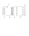
- FIG. 10 is an equivalent circuit diagram showing an example of a non-contact coupling circuit for explaining the principle of the non-contact transmission mechanism.
- the transmission / reception circuit of an external read / write device (reading device) (not shown) used in a non-contact type is an electromagnetic coupler that is an electromagnetic coupler that supplies power to the non-contact transmission mechanism of the composite IC card and transfers information.
- the coil is connected.
- the non-contact transmission mechanism of the composite IC card includes an antenna coil 7a, a capacitive element 8 connected to both ends of the antenna coil 7a to form a parallel resonance circuit, a composite IC chip 4b mounted on the composite IC module 4,
- the first coupling coil 5a and the second coupling coil 6a are connected to the composite IC chip 4b.
- the antenna coil 7a is directly electromagnetically coupled to a transmission / reception antenna of an external read / write device, and is involved in power reception and information transmission / reception.
- the second coupling coil 6a is closely coupled to the first coupling coil 5a in order to transmit the signal received by the antenna coil with the maximum efficiency, and is connected to the capacitive element 8 constituting the parallel resonance circuit.
- the second coupling coil 6a and the capacitive element 8 are connected at a junction land 10 as shown in FIGS.
- the second coupling coil 6 a formed on the surface 2 a of the antenna sheet 2 and the wiring 8 a drawn from the capacitive element 8 and formed on the back surface 2 b of the antenna sheet 2 are formed on the surface 2 a of the antenna sheet 2. They are connected at the formed junction land 10. More specifically, for example, the bonding lands 10 formed on the surface 2a of the antenna sheet 2 are mechanically pressed, whereby the second coupling coil 6a formed on the surface 2a of the antenna sheet 2 and the antenna sheet 2 are The wiring 8a formed on the back surface 2b can be physically connected.
- the bonding land 10 can be irradiated with laser light to weld the second coupling coil 6 a and the wiring 8 a of the capacitive element 8.
- an appropriate method can be employed for the connection.
- the second coupling coil 6a is formed on the surface 2a of the antenna sheet 2
- the wiring 8a of the capacitive element 8 is formed on the surface 2a of the antenna sheet 2.
- the arrangement is not limited, and an appropriate arrangement can be taken according to the required characteristics of the IC card.
- the capacitive element 8 and the antenna coil 7a are connected in series in the examples shown in FIGS. 5 and 6, but the capacitive element 8 is connected in parallel between the antenna coil 7a and the second coupling coil 6a. Is also suitable. Further, the capacitive element 8 can be omitted by increasing the line capacitance.
- a method for transmitting power and information from an external read / write device to the composite IC card and the coupling of the coils used in the method will be described below.
- a high frequency magnetic field is induced in the transmission / reception coil by a high frequency signal (not shown) generated in the transmission / reception circuit of the external read / write device. This high frequency signal is radiated into space as magnetic energy.
- a current due to a high frequency magnetic field is induced in 6a.
- the reception sensitivity of the composite IC card is the antenna coil 7a. It depends greatly on the characteristics of
- a signal received by a resonance circuit composed of the antenna coil 7a and the capacitive element 8 is transmitted to the second coupling coil 6a. Thereafter, since the second coupling coil 6a and the first coupling coil 5a are closely coupled to each other to exhibit the maximum transmission efficiency, the second coupling coil 6a and the first coupling coil 5a are coupled to the composite IC chip 4b by the transformer coupling. A signal is transmitted.
- the maximum transmission efficiency of the transformer coupling between the second coupling coil 6a and the first coupling coil 5a is determined by the selection of circuit constants. As described above, the reception characteristics are improved. As described above, since the characteristics of the antenna coil 7a determine the reception sensitivity of the composite IC card, the larger the area of the antenna coil 7a, the more advantageous the reception sensitivity.
- the line width (thickness), the interval, and the number of turns of the antenna coil can be appropriately set according to the characteristics of the antenna coil and restrictions due to the arrangement.
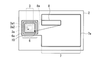
- the composite IC card according to this embodiment includes a card base 1 having an antenna sheet 2 including an IC module 4, a second coupling coil 6a, and an antenna coil 7a.
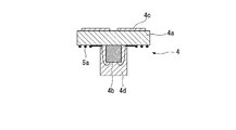
- the composite IC module 4 includes an IC chip having both a contact-type transmission function and a non-contact-type transmission function, a module substrate on which external terminals that are contact-type transmission elements are formed, and a non-contact transmission mechanism. 1 coupling coil. More specifically, the composite IC module 4 includes a composite IC chip 4b incorporating a contact type interface and a non-contact type interface, a terminal electrode (external terminal) 4c which is a contact type transmission unit (external terminal), A module substrate 4a having a pattern formed on different surfaces of the first coupling coil 5a of the non-contact transmission unit.
- the first coupling coil 5a and the antenna coil 7a a metal thin film pattern formed by etching a metal thin film, a so-called winding coil wound with an insulating coated conductor, or conductive A coil printed with ink may be used.
- the composite IC chip 4 is mounted on the surface on which the first coupling coil 5a of the module substrate 4a is formed.
- the composite IC chip 4b and the terminal electrode 4c of the module substrate 4a are connected through a through hole.
- an etching antenna that is easily formed by etching is used as the coil of the second coupling coil region 6 and the antenna coil region 7. preferable.
- the line width of the coil formed by fine processing such as etching as described above and the interval between adjacent coils are each 0.1 mm or more.
- the second coupling coil 6a in the second coupling coil region 6 is a coil whose line and space is approximately 0.4 to 0.5 mm. be able to.
- the circuit pattern of the composite IC chip 4b and the circuit pattern of the first coupling coil 5a is formed by wire bonding.
- the connection between the composite IC chip 4b and the first coupling coil 5a is also realized by thermally welding the circuit formation surface of the composite IC chip 4b and the module substrate 4a using solder or a conductive adhesive.
- the composite IC chip 4b is mounted on the module substrate 4a and connected to the circuit, the composite IC chip 4b is sealed with a sealing resin 4d to complete the composite IC module 4.
- the composite IC card 100 is manufactured generally as follows. First, the flexible antenna sheet 2 in which the second coupling coil 6a, the antenna coil 7a, and the capacitive element 8 are formed on the sheet base material by etching a metal thin film or the like is prepared.
- the second coupling coil 6a and the antenna coil 7a may be formed by winding a conductive wire with insulation coating.
- vinyl chloride, polyimide, polycarbonate, polyethylene terephthalate (PET), polyethylene naphthalate (PEN), or the like can be used for the sheet base material of the antenna sheet 2.
- the card substrate 1 has a plurality of layers.
- the card substrate 1 has a pair of core substrates 1a and a pair of exterior substrates 1b arranged on both sides of the core substrate 1a.
- the antenna sheet 2 is sandwiched between the core base materials 1a, and they are integrated by thermal lamination.
- Any card base material 1 can be used as long as it provides the card with sufficient strength and embossing properties, such as vinyl chloride, amorphous polyester (PETG), and polycarbonate.
- a recess 3a for embedding the composite IC module 4 is formed by milling, cutting, or the like.
- the composite IC module 4 as shown in FIGS. 3A and 3B is completed by embedding and bonding the composite IC module 4 in the recess 3a of the card base.
- the second coupling coil 6 a formed on the antenna sheet 2 is disposed outside the recessed area 3 formed on the card base 1.
- a method such as milling or cutting for forming the recess 3a by cutting the card substrate 1 with a cutting tool
- the depth of the processing device is obtained when the second coupling coil 6a is disposed in the recess region 3.
- the cutting tool may reach the second coupling coil 6a and the second coupling coil 6a may be disconnected, or the second coupling coil 6a due to the distortion of the antenna sheet without disconnection.
- desired characteristics may not be obtained due to the deformation.
- since the 2nd coupling coil 6a is arrange
- the end 2 c of the antenna sheet 2 may be disposed outside the recessed area 3.
- damage or deformation of the end 2c of the antenna sheet 2 due to milling, cutting, or the like that cuts the card substrate 1 to form the recess 3a can be reliably prevented. That is, it is possible to reliably prevent the deformation of the second coupling coil 6a accompanying the damage or deformation of the end 2c of the antenna sheet 2 and the resulting deterioration of the characteristics of the second coupling coil 6a.
- the recess 3a of the recess area 3 has a first recess 3a1 formed in the vicinity of the surface of the card base and an opening width communicating with the first recess 3a1 and narrower than the first recess 3a1. It can comprise from two recessed part 3a2.
- the size of the first recess 3a1 corresponds to the size of the module substrate 4a shown in FIG. 2, and the size of the second recess 3a2 is the sealing shown in FIG. This corresponds to the size of the resin 4d.
- the antenna sheet 2 is arranged outside the opening of the first recess 3a1.
- the central axis of the first concave portion 3a1 and the central axis of the second concave portion 3a2 substantially coincide with each other in the depth direction.
- a first recess 3a1 and a second recess 3a2 are formed.
- the shape and size of the recess 3a are not limited to those described above, and can be appropriately changed according to the shape and size of the IC module 4 embedded in the card substrate 1.
- the second coupling coil 6a can be formed at a position deeper than the depth of the recess 3a formed in the recess region 3 (that is, the bottom surface 3b of the recess 3a). According to such a configuration, since the influence of milling and cutting on the second coupling coil 6a is reduced, disconnection and deformation of the second coupling coil 6a can be prevented. According to the configuration in which the second coupling coil 6a of the antenna sheet 2 is arranged outside the recessed region 3 as shown in FIG. 9A, the disconnection and deformation of the second coupling coil 6a can be prevented more reliably. Can do.
- the second coupling coil 6a of the antenna sheet 2 is disposed at a position sufficiently deeper than the bottom surface 3b of the recess 3a, a part of the second coupling coil 6a as shown in FIG. 9B is recessed. Even in the configuration arranged inside the region 3, disconnection and deformation of the second coupling coil 6 a can be prevented.
- connection land 10 that connects the second coupling coil 6a and the wiring 8a of the capacitive element 8 may be disposed inside the recessed region 3.
- a part of the connection land 10 is disposed between the side wall 3a11 of the first recess 3a1 and the side wall 3a21 of the second recess 3a2. That is, a part of the connection land 10 is disposed in the first recess 3a1 and outside the second recess in plan view.
- the entire connection land 10 may be disposed in the first recess 3a1 and outside the second recess in plan view.
- connection land 10 has a width larger than the line width of the coil forming the second coupling coil 6a in plan view. It is formed to have. Therefore, even if the connection land 10 is disposed inside the recessed area 3, disconnection / deformation due to milling or cutting for forming the recessed area 3 is unlikely to occur. Further, the second coupling coil 6 a can be brought closer to the recessed area 3 by arranging the connection land 10 inside the recessed area 3. That is, the distance between the second coupling coil 6a and the first coupling coil 5a of the IC module 4 disposed in the recessed area 3 can be made closer. As a result, the coupling between the second coupling coil 6a and the first coupling coil 5a can be further improved.
- connection land 10 is preferably approximately 3 to 5 mm in diameter.
- the connection land 10 is preferably approximately 2 to 4 mm in diameter.
- the processing area is approximately 0.5 to 1.5 mm in diameter. Therefore, in consideration of processing variations, the connection land 10 is preferably approximately 2 to 4 mm in diameter.
- welding may be performed by irradiating a plurality of locations on the connection land 10 with laser in order to increase the connection reliability between the second coupling coil 6 a and the capacitive element 8.
- connection land 10 is, for example, several times to several tens of times the line width of the adjacent second coupling coil 6a for the reasons described above. Therefore, when the entire connection land 10 is disposed outside the recessed area 3, the second coupling coil 6 a adjacent to the connection land 10 is compared with the case where the connection land 10 is disposed within the recessed area 3. The distance between the IC module 4 and the first coupling coil 5a disposed in the recessed area 3 is increased, and as a result, the electromagnetic coupling between the second coupling coil 6a and the first coupling coil 5a is weakened.
- the second coupling coil region 6 having the second coupling coil 6a as shown in FIG. 5 may be arranged outside the antenna coil region 7 including the antenna coil 7a, or the second coupling coil region 6 as shown in FIG.
- the coupling coil region 6 may be disposed inside the antenna coil region 7. Since the position of the contact terminal of the IC module is defined by ISO, the number of turns of the second coupling coil region 6 is limited, and it is difficult to improve the characteristics. However, in the configuration in which the second coupling coil region 6 is disposed outside the antenna coil region 7, the degree of freedom in designing the number of turns of the second coupling coil region 6 can be ensured. When the second coupling coil region 6 is disposed inside the antenna coil region 7, the design freedom of the number of turns of the second coupling coil region 6 is reduced, but the area of the antenna coil is increased. For this reason, the communication characteristic as an antenna can be improved.
- the width of the innermost coil of the second coupling coil 6a can be made larger than the width of the other coils.
- the width of the innermost coil is not particularly limited, but is preferably about 1.2 to 5 times the width of the other coils. If the width of the innermost coil is thinner than the above, the effect is low, and if it is thicker than the above, the number of turns of the coil cannot be increased.
- the width of the innermost coil is more preferably about 1.5 to 3 times the width of the other coils.
- the line width of the coil 6a1 formed at the lower portion can be made wider than the others.
- stress tends to concentrate on the edge of the recess 3a, so that the coil formed on the innermost periphery of the second coupling coil 6a is likely to break.
- the vicinity of the coil 6a1 that is formed along the longitudinal direction of the composite IC card 100 and is closest to the center in the short direction of the composite IC card 100 has the largest curvature when the composite IC card 100 is bent. Become.
- the coil 6a1 has a wider line width than the others.
- the coils formed on the innermost periphery of the second coupling coil 6a when the coil formed on the upper part is provided at a position closer to the center in the short direction of the composite IC card 100, You may form the line
- the portion of the antenna sheet 2 where the second coupling coil 6a and the capacitive element 8 are not formed can be punched out.
- the substrates on both sides of the antenna sheet 2 can be fused together via the punched portion 9 of the antenna sheet 2, so Can be pasted together.
- PET or PEN used as the base material of the antenna sheet 2 may be difficult to be fused with the card base material 1. Therefore, when the antenna sheet 2 that does not have the punched-out portion 9 and the card base material 1 are bonded together by heat lamination, the antenna sheet 2 and the base material adjacent to the antenna sheet 2 are not sufficiently fused, and thus obtained.
- the composite IC card 100 is bent, the antenna sheet 2 and the card base 1 may be peeled off.
- the composite IC card 100 according to the present embodiment can be formed with a magnetic stripe or embossed. It is preferable to arrange the magnetic stripe forming region and the embossing region so as not to overlap the antenna coil 7a. Furthermore, the composite IC card 100 according to the present embodiment can be provided with a functional layer to which a functional transfer foil such as a picture layer or a hologram is transferred.
- the line width can be made thicker than others. In this case, it is preferable that the line width of the coil provided at the position corresponding to the area where the character is printed is formed larger than the height of the character printed by embossing. More specifically, the standard specifies that the height of characters printed on the surface of the composite IC card 10 is 3 mm or 5 mm depending on the area where the characters are formed.
- the line width of the coil provided at the position corresponding to the area where the characters are printed is 3 mm or more or 5 mm or more depending on the area.
- the substrate polyethylene terephthalate having a thickness of 80 ⁇ m and having an aluminum thin film formed on both sides was used.
- the second coupling coil 6a, the antenna coil 7a, and a part of the capacitive element 8 are formed by etching on one surface of the substrate, and the remaining part of the capacitive element 8 and the jumper wire are formed by etching on the other surface.
- an antenna sheet 2 was obtained.
- the second coupling coil 6a and the antenna coil 7a were formed to have a line width of 1 mm.
- the second coupling coil region 6 was provided outside the antenna coil region 7.
- the second coupling coil 6a was formed so that the number of turns was 3 turns, and the antenna coil 7a was formed so that the number of turns was 1 turn.
- the 2nd coupling coil 6a was arrange
- the second coupling coil 6a was formed such that the innermost line width of the second coupling coil region 6 was 2 mm.
- the punching process was performed to the part in which the 2nd coupling coil 6a, the antenna coil 7a, etc. are not formed.
- a card composed of a two-layer core substrate 1a made of polyvinyl chloride (PVC) having a thickness of 0.6 mm and an exterior substrate 1b made of amorphous polyester having a thickness of 0.1 mm on both surfaces of the core substrate.
- PVC polyvinyl chloride
- a substrate 1 was prepared.
- the above-described antenna sheet 2 was sandwiched between the core base material 1a, and these were bonded together by thermal lamination at a temperature of 100 to 120 ° C., thereby producing a card base material 1.
- the recessed part 3 which has the recessed part 3a of the 2 step
- the IC module 4 was placed in the recess 3a using a pickup device, and the IC module 4 was mounted on the card substrate 1 by hot pressing to obtain a composite IC card 100.
- the first coupling coil 5a was formed so that the number of turns was 3 turns.
- the IC module 4 of the obtained composite IC card 100 was removed, and the state of the innermost circumference of the second coupling coil 6a was confirmed. It was confirmed that there was no disconnection or deformation of the second coupling coil 6a.
- an IC module having both a contact type and a non-contact type function and including a coil, and a card base in order to be electrically connected to the coil formed on the IC module in a non-contact manner.
- a composite IC card comprising a coil provided in the antenna and an antenna coil for non-contact communication with an external terminal, defects due to disconnection or deformation of the coil for electrical connection with the coil of the IC module Can be reduced.
Landscapes
- Engineering & Computer Science (AREA)
- Microelectronics & Electronic Packaging (AREA)
- Computer Hardware Design (AREA)
- Physics & Mathematics (AREA)
- General Physics & Mathematics (AREA)
- Theoretical Computer Science (AREA)
- Computer Networks & Wireless Communication (AREA)
- Credit Cards Or The Like (AREA)
- Near-Field Transmission Systems (AREA)
- Variable-Direction Aerials And Aerial Arrays (AREA)
Abstract
凹部を有するカード基材と;前記カード基材の内部に配置されたアンテナシートと;前記カード基材の凹部内に配置されたICモジュールと;を備える複合ICカードであって、前記ICモジュールは、接触型伝達機能と非接触型伝達機能との双方の機能を備えたICチップと、接触型伝達素子である外部端子が形成されたモジュール基板と、非接触伝達機構である第1の結合コイルと、を有し、前記アンテナシートは、外部の読み取り装置との間で電力の受給と信号の授受を行うアンテナコイルと、前記アンテナコイルに接続された第2の結合コイルと、を有し、前記第1の結合コイルと前記第2の結合コイルとが、互いに密結合可能に配設されて前記ICモジュールと前記アンテナシートとがトランス結合によって非接触な結合が可能に構成され、前記アンテナシートの前記第2の結合コイルが、前記カード基材の凹部が形成されている領域よりも外に配置されている。
Description
本発明は、電源電力の受給、電気接点を介して信号の授受等を行う接触型、及び電源電力の受給、信号の授受等をICカードに電気接点を設けることなく電磁結合方式によって非接触状態で行う非接触型の双方として機能する複合ICカード、及びその製造方法に関する。
本願は、2011年11月17日に、日本に出願された特願2011-251437号に基づき優先権を主張し、その内容をここに援用する。
本願は、2011年11月17日に、日本に出願された特願2011-251437号に基づき優先権を主張し、その内容をここに援用する。
半導体メモリー等を内蔵するICカードとして、接触型及び非接触型の双方として機能する、いわゆる複合ICカード(デュアルICカード)が知られている。このような複合ICカードとして、外部の端末と非接触通信するためにカード内に設けられたアンテナコイルと、接触型及び非接触型の双方として機能するICモジュールとを物理的に配線で接続した複合ICカードがある。
また、接触型及び非接触型の双方として機能するICモジュールにコイルが形成され、このICモジュールに形成されたコイルと非接触で電気的に結合するためのコイルと外部の端末と非接触通信するためのアンテナコイルとがカード内に設けられた複合ICカードがある(特許文献1、2、3参照)。
また、接触型及び非接触型の双方として機能するICモジュールにコイルが形成され、このICモジュールに形成されたコイルと非接触で電気的に結合するためのコイルと外部の端末と非接触通信するためのアンテナコイルとがカード内に設けられた複合ICカードがある(特許文献1、2、3参照)。
後者の複合ICカードは、ICモジュールとアンテナコイルとを物理的に配線で接続する必要がなく、接触不良等の不良がおきにくいため、近年需要が増加している。このようなICカードは、アンテナコイルとICモジュールのコイルと電気的に接続するためのコイルとを内部に有するカード基材を作製し、その後ミリング加工などによりICモジュールを埋設するための凹部をカード基材に形成し、形成された凹部内にICモジュールを埋設配置することにより得られる。
カード基材に凹部を形成するとき、ICモジュールのコイルと電気的に接続するためのコイルの位置や加工装置の精度によって、コイルの断線や変形などを起こす可能性がある。
カード基材に凹部を形成するとき、ICモジュールのコイルと電気的に接続するためのコイルの位置や加工装置の精度によって、コイルの断線や変形などを起こす可能性がある。
本発明は、接触型及び非接触型の双方として機能しコイルを備えたICモジュールと、ICモジュールに形成されたコイルと非接触で電気的に結合するためのコイル及び外部の端末と非接触通信するためのアンテナコイルとがカード基材内に設けられた複合ICカードにおいて、ICモジュールのコイルと電気的に接続するためのコイルの断線や変形などによる不良を低減できる複合ICカードの提供を課題とする。
上述した課題を解決するために、本発明の一態様に係る複合ICカードは、凹部を有するカード基材と;前記カード基材の内部に配置されたアンテナシートと;前記カード基材の凹部内に配置されたICモジュールと;を備え、前記ICモジュールは、接触型伝達機能と非接触型伝達機能との双方の機能を備えたICチップと、接触型伝達素子である外部端子が形成されたモジュール基板と、非接触伝達機構である第1の結合コイルと、を有し、前記アンテナシートは、外部の読み取り装置との間で電力の受給と信号の授受を行うアンテナコイルと、前記アンテナコイルに接続された第2の結合コイルと、を有し、前記第1の結合コイルと前記第2の結合コイルとが、互いに密結合可能に配設されて前記ICモジュールと前記アンテナシートとがトランス結合によって非接触な結合が可能に構成され、前記アンテナシートの前記第2の結合コイルが、前記カード基材の凹部が形成されている領域よりも外に配置されている。
前記第2の結合コイルが複数周巻回されたコイルから形成され、最内周の前記コイルの線幅が、最内周以外のコイルの線幅よりも太くてもよい。
前記アンテナシートが、前記第2の結合コイル及び前記アンテナコイルと接続された容量性素子をさらに有してもよい。
前記第2の結合コイルは前記アンテナシートの表面に形成され、前記アンテナシートは、前記第2の結合コイルと、前記容量性素子から引き出され前記アンテナシートの裏面に形成された配線とを接続する接続ランドをさらに有し、前記接続ランドは、前記カード基材の凹部が形成されている領域の内に配置されていてもよい。
前記カード基材の凹部は、前記カード基材の表面近傍に形成された第一凹部と、前記第一凹部に連通し前記第一凹部よりも狭い開口幅を有する第二凹部とから構成され、前記接続ランドは、前記第一凹部の側壁と前記第二凹部の側壁との間に配置されていてもよい。
前記接続ランドの幅は、平面視において、前記第2結合コイルの線幅よりも大きくてもよい。
前記アンテナシートが、前記カード基材の凹部の底面よりも深い位置に配置されていてもよい。
上記本発明の態様によれば、ICモジュールのコイルと電気的に接続するためのコイルの断線や変形などによる不良を低減することができる。
以下、図面を参照して本発明の一実施形態にかかる複合ICカードを説明する。
先ず、非接触伝達機構の基本的構成と基本原理について説明する。
図10は、非接触伝達機構の原理を説明するための非接触結合回路の一例を示す等価回路図である。非接触型で用いられる外部の読み書き装置(読み取り装置)(図示せず)の送受信回路には、複合ICカードの非接触伝達機構への電力供給と情報の授受とを行う電磁結合器である送受信コイルが接続されている。
複合ICカードの非接触伝達機構は、アンテナコイル7aと、アンテナコイル7aの両端に接続されて並列共振回路を構成する容量性素子8と、複合ICモジュール4に実装された複合ICチップ4bと、複合ICチップ4bに接続された第1結合コイル5aと、第2結合コイル6aと、を有する。アンテナコイル7aは、外部の読み書き装置の送受信アンテナと直接、電磁的に結合され電力の受信と情報の授受に関与する。第2結合コイル6aは、第1結合コイル5aにアンテナコイルで受信した信号を最大効率で伝送するために密結合配置され、並列共振回路を構成する容量性素子8に接続されている。
第2結合コイル6aと容量性素子8とは、図5,6,11A及び11Bに示されているように、接合ランド10において接続されている。図示例では、アンテナシート2の表面2aに形成された第2結合コイル6aと、容量性素子8から引き出されアンテナシート2の裏面2bに形成された配線8aとが、アンテナシート2の表面2aに形成された接合ランド10において接続されている。より具体的には、たとえば、アンテナシート2の表面2aに形成された接合ランド10を機械的に押圧することにより、アンテナシート2の表面2aに形成された第2結合コイル6aとアンテナシート2の裏面2bに形成された配線8aとを物理的に接続することができる。接合ランド10にレーザー光を照射して第2結合コイル6aと容量性素子8の配線8aとを溶接することもできる。その他、上記接続には、適宜の方法を採用することができる。
図示例において、第2結合コイル6aはアンテナシート2の表面2aに形成され、容量性素子8の配線8aはアンテナシート2の表面2aに形成されているが、これらの配置関係は、上記例に限られず、要求されるICカードの特性に応じて、適宜の配置をとることができる。
図示例において、第2結合コイル6aはアンテナシート2の表面2aに形成され、容量性素子8の配線8aはアンテナシート2の表面2aに形成されているが、これらの配置関係は、上記例に限られず、要求されるICカードの特性に応じて、適宜の配置をとることができる。
容量性素子8とアンテナコイル7aとの接続は、図5、6に示す例では直列であるが、アンテナコイル7aと第2の結合コイル6aとの間に並列に容量性素子8を接続することも好適である。また、線間容量を増大させることで容量性素子8を省略することも可能である。
外部の読み書き装置から複合ICカードに電力および情報を伝達する方法及び、それに用いる各コイルの結合について以下に説明する。
外部読み書き装置の送受信回路で発生した図示しない高周波信号により、送受信コイルに高周波磁界が誘起される。この高周波信号は、磁気エネルギーとして空間に放射される。
外部読み書き装置の送受信回路で発生した図示しない高周波信号により、送受信コイルに高周波磁界が誘起される。この高周波信号は、磁気エネルギーとして空間に放射される。
外部読み書き装置の送受信コイルにより発生し高周波磁界により、この高周波磁界中に位置する複合IC力一ドの、アンテナコイル7aと容量性素子8とで構成される並列共振回路に電流が流れる。このとき、複合ICチップ4bに直接接続された第1結合コイル5aと、アンテナコイル7aと容量性素子8とで構成される共振回路に接続され第1結合コイル5aに電力伝送する第2結合コイル6aと、に高周波磁界による電流が誘起される。第1結合コイル5aと第2結合コイル6aとに誘起される電流の量は、アンテナコイル7aに誘起される電流の量に比べて一桁以上小さいので、複合ICカードの受信感度はアンテナコイル7aの特性に大きく依存する。
アンテナコイル7aと容量性素子8とで構成された共振回路で受信した信号は第2結合コイル6aに伝達される。その後、第2結合コイル6aと第1結合コイル5aとが最大伝達効率を示す密結合配置されているので、第2結合コイル6aと第1結合コイル5aとのトランス結合によって、複合ICチップ4bに信号が伝達される。第2結合コイル6aと第1結合コイル5aとのトランス結合の最大伝達効率は回路定数の選択によって決定される。
以上のように、受信特性の改善が達成される。上述の通り、アンテナコイル7aの特性が複合ICカードの受信感度を決定するため、アンテナコイル7aの面積は大きいほど受信感度の点で有利である。アンテナコイルの線幅(太さ)、間隔、巻数は、アンテナコイルの特性や配置による制限などに応じて適宜設定できる。
以上のように、受信特性の改善が達成される。上述の通り、アンテナコイル7aの特性が複合ICカードの受信感度を決定するため、アンテナコイル7aの面積は大きいほど受信感度の点で有利である。アンテナコイルの線幅(太さ)、間隔、巻数は、アンテナコイルの特性や配置による制限などに応じて適宜設定できる。
本実施形態に係る複合ICカードは、ICモジュール4と第2結合コイル6aとアンテナコイル7aとを含むアンテナシート2を有するカード基材1を備える。
複合ICモジュール4は、接触型伝達機能と非接触型伝達機能との双方の機能を有するICチップと、接触型伝達素子である外部端子が形成されたモジュール基板と、非接触伝達機構である第1の結合コイルとを備える。より具体的に、複合ICモジュール4は、接触型インターフェースと非接触型インタフェ一スとを内蔵した複合ICチップ4bと、接触型伝達部(外部端子)である端子電極(外部端子)4cと、非接触型伝達部の第1結合コイル5aと、を相異なる面にパターン形成したモジュール基板4aとを備える。
第1結合コイル5a及びアンテナコイル7aには、金属薄膜のエッチングにより形成された金属薄膜パターンを用いてもよいし、絶縁被覆した導線を巻いたいわゆる巻線コイルを用いてもよいし、導電性インキを印刷したコイルを用いてもよい。複合ICチップ4は、モジュール基板4aの第1結合コイル5aが形成されている面に実装される。複合ICチップ4bとモジュール基板4aの端子電極4cとはスルーホールを介して接続される。
また、容量性素子8の配線をアンテナシート2の表面及び裏面に配置する場合には、エッチングにより容易に形成されるエッチングアンテナを第2結合コイル領域6及びアンテナコイル領域7のコイルとして用いることが好ましい。
また、上述のようなエッチング等の微細加工により形成されるコイルの線幅及び隣接するコイル間の間隔は、それぞれ0.1mm以上であることが好ましい。特に、第2結合コイル領域6の第2結合コイル6aには、コイルの線幅と隣接するコイル間の間隔との合計(line and space)が0.4~0.5mm程度であるコイルを用いることができる。
また、容量性素子8の配線をアンテナシート2の表面及び裏面に配置する場合には、エッチングにより容易に形成されるエッチングアンテナを第2結合コイル領域6及びアンテナコイル領域7のコイルとして用いることが好ましい。
また、上述のようなエッチング等の微細加工により形成されるコイルの線幅及び隣接するコイル間の間隔は、それぞれ0.1mm以上であることが好ましい。特に、第2結合コイル領域6の第2結合コイル6aには、コイルの線幅と隣接するコイル間の間隔との合計(line and space)が0.4~0.5mm程度であるコイルを用いることができる。
複合ICチップ4bと第1結合コイル5aの回路パターンとはワイヤボンドされて回路が形成されている。この複合ICチップ4bと第1結合コイル5aとの接続は、複合ICチップ4bの回路形成面とモジュール基板4aとを半田や導電性接着剤を用いて熱溶着することによっても実現される。
複合ICチップ4bをモジュール基板4aに実装し、回路接続された後に、複合ICチップ4bは封止樹脂4dにより封止され複合ICモジュール4が完成する。
本実施形態にかかる複合ICカード100は概略以下のようにして製作される。
まず、シート基材に金属薄膜のエッチング等により第2結合コイル6aとアンテナコイル7aと容量性素子8を形成したフレキシブルなアンテナシート2が準備される。第2結合コイル6aとアンテナコイル7aとは絶縁被覆した導線を巻いて形成してもよい。
アンテナシート2のシート基材には、例えば塩化ビニル、ポリイミド、ポリカーボネート、ポリエチレンテレフタレート(PET)、ポリエチレンナフタレート(PEN)などを用いることができる。
まず、シート基材に金属薄膜のエッチング等により第2結合コイル6aとアンテナコイル7aと容量性素子8を形成したフレキシブルなアンテナシート2が準備される。第2結合コイル6aとアンテナコイル7aとは絶縁被覆した導線を巻いて形成してもよい。
アンテナシート2のシート基材には、例えば塩化ビニル、ポリイミド、ポリカーボネート、ポリエチレンテレフタレート(PET)、ポリエチレンナフタレート(PEN)などを用いることができる。
次に、アンテナシート2とカード基材1とを貼り合わせる。カード基材1は複数の層を有する。図1の例において、カード基材1は、1対のコア基材1aとコア基材1aの両側に配された1対の外装基材1bとを有する。コア基材1aの間にアンテナシート2が挟みこまれ、熱ラミネートによりそれらが一体化される。
カード基材1には、塩化ビニル、非晶質ポリエステル(PETG)、ポリカーボネートなど、十分な強度やエンボス性などのカードに必要な特性が得られるもので有れば何でも用いることができる。
カード基材1には、塩化ビニル、非晶質ポリエステル(PETG)、ポリカーボネートなど、十分な強度やエンボス性などのカードに必要な特性が得られるもので有れば何でも用いることができる。
アンテナシート2を有するカード基材1を作製した後に、ミリング加工、切削加工等により複合ICモジュール4を埋設するための凹部3aを形成する。
次に、カード基材の凹部3aに複合ICモジュール4を埋設し接着することで、図3A及び3Bに示したような複合ICカード100が完成する。
次に、カード基材の凹部3aに複合ICモジュール4を埋設し接着することで、図3A及び3Bに示したような複合ICカード100が完成する。
本実施形態にかかる複合ICカード100では、アンテナシート2に形成されている第2結合コイル6aが、カード基材1に形成した凹部領域3の外側に配置されている。
切削工具を用いてカード基材1を削り凹部3aを形成するミリング加工、切削加工等の方法を用いる場合、凹部領域3内に第2結合コイル6aが配置されていると、加工装置の深さ方向の精度や横方向の精度によっては、切削工具が第2結合コイル6aに達して、第2結合コイル6aが断線する可能性や、断線しなくてもアンテナシートの歪みによる第2結合コイル6aの変形により所望の特性が得られなくなる可能性などがある。
本実施形態では、第2結合コイル6aが凹部領域3の外側に配置されているため、上述の断線やコイル変形を防ぐことができる。
切削工具を用いてカード基材1を削り凹部3aを形成するミリング加工、切削加工等の方法を用いる場合、凹部領域3内に第2結合コイル6aが配置されていると、加工装置の深さ方向の精度や横方向の精度によっては、切削工具が第2結合コイル6aに達して、第2結合コイル6aが断線する可能性や、断線しなくてもアンテナシートの歪みによる第2結合コイル6aの変形により所望の特性が得られなくなる可能性などがある。
本実施形態では、第2結合コイル6aが凹部領域3の外側に配置されているため、上述の断線やコイル変形を防ぐことができる。
さらに、図1に示されているように、アンテナシート2の端部2cが凹部領域3の外側に配置されていてもよい。この場合、カード基材1を削り凹部3aを形成するミリング加工、切削加工等による、アンテナシート2の端部2cの損傷や変形等を確実に防ぐことができる。すなわち、アンテナシート2の端部2cの損傷や変形等に伴う第2結合コイル6aの変形、及び、その結果もたらされる第2結合コイル6aの特性の劣化を確実に防ぐことができる。
凹部領域3の凹部3aは、図1に示すように、カード基材の表面近傍に形成された第一凹部3a1と、第一凹部3a1に連通し第一凹部3a1よりも狭い開口幅を有する第二凹部3a2と、から構成することができる。図1の例では、第一凹部3a1の大きさが、図2に示されているモジュール基板4aの大きさに対応し、第二凹部3a2の大きさが、図2に示されている封止樹脂4dの大きさに対応している。図1の例において、アンテナシート2は、第一凹部3a1の開口部の外側に配置されている。
また、図1の例では、図2に示されているICモジュール4に対応して、深さ方向について第一凹部3a1の中心軸と第二凹部3a2の中心軸とが実質的に一致するように、第一凹部3a1と第二凹部3a2とが形成されている。しかしながら、凹部3aの形状及び大きさは、上述に限られず、カード基材1に埋設されるICモジュール4の形状及び大きさに応じて適宜変更可能である。
また、図1の例では、図2に示されているICモジュール4に対応して、深さ方向について第一凹部3a1の中心軸と第二凹部3a2の中心軸とが実質的に一致するように、第一凹部3a1と第二凹部3a2とが形成されている。しかしながら、凹部3aの形状及び大きさは、上述に限られず、カード基材1に埋設されるICモジュール4の形状及び大きさに応じて適宜変更可能である。
また、第2結合コイル6aは、図9A及び9Bに示すように、凹部領域3に形成された凹部3aの深さ(すなわち、凹部3aの底面3b)よりも深い位置に形成することができる。
このような構成によれば、ミリング加工、切削加工が第2結合コイル6aに及ぼす影響が低減するため、第2結合コイル6aの断線、変形を防ぐことができる。図9Aに示されているような、アンテナシート2の第2結合コイル6aが凹部領域3の外側に配置されている構成によれば、第2結合コイル6aの断線、変形をより確実に防ぐことができる。また、アンテナシート2の第2結合コイル6aが、凹部3aの底面3bよりも十分に深い位置に配置されていれば、図9Bに示されているような第2結合コイル6aの一部が凹部領域3の内側に配置されている構成においても、第2結合コイル6aの断線、変形を防ぐことができる。
このような構成によれば、ミリング加工、切削加工が第2結合コイル6aに及ぼす影響が低減するため、第2結合コイル6aの断線、変形を防ぐことができる。図9Aに示されているような、アンテナシート2の第2結合コイル6aが凹部領域3の外側に配置されている構成によれば、第2結合コイル6aの断線、変形をより確実に防ぐことができる。また、アンテナシート2の第2結合コイル6aが、凹部3aの底面3bよりも十分に深い位置に配置されていれば、図9Bに示されているような第2結合コイル6aの一部が凹部領域3の内側に配置されている構成においても、第2結合コイル6aの断線、変形を防ぐことができる。
図11A及び11Bに示すように、第2結合コイル6aと容量性素子8の配線8aとを接続する接続ランド10は、凹部領域3の内側に配置してもよい。図11A及び11Bの例では、接続ランド10の一部が第一凹部3a1の側壁3a11と第二凹部3a2の側壁3a21との間に配置されている。すなわち、接続ランド10の一部は、平面視において、第一凹部3a1の内であって第二凹部の外に配置されている。接続ランド10の全体を平面視において、第一凹部3a1の内であって第二凹部の外に配置してもよい。
接続ランド10は、上述のような第2結合コイル6aと容量性素子8との接続を確実に行うために、平面視において、第2結合コイル6aを形成するコイルの線幅よりも大きい幅を有するように形成されている。したがって、接続ランド10は、凹部領域3の内側に配置されていても、凹部領域3を形成するためのミリング加工や切削加工等による断線・変形が生じにくい。
また、接続ランド10を凹部領域3の内側に配置することにより、第2結合コイル6aを凹部領域3により近づけることができる。すなわち、第2結合コイル6aと、凹部領域3内に配置されるICモジュール4の第1結合コイル5aとの距離をより近づけることができる。その結果、第2結合コイル6aと第1結合コイル5aとの結合をより向上させることができる。
また、接続ランド10を凹部領域3の内側に配置することにより、第2結合コイル6aを凹部領域3により近づけることができる。すなわち、第2結合コイル6aと、凹部領域3内に配置されるICモジュール4の第1結合コイル5aとの距離をより近づけることができる。その結果、第2結合コイル6aと第1結合コイル5aとの結合をより向上させることができる。
接続ランド10における第2結合コイル6aと容量性素子8との接続には、かしめ加工、抵抗溶接加工、レーザー溶接加工等を用いることができる。
かしめ加工を用いる場合には、その加工領域がおおよそ直径1~3mm程度であるため、加工のばらつきを考慮すると、接続ランド10は直径3~5mm程度であることが好ましい。抵抗溶接加工を用いる場合には、その加工領域がおおよそ直径0.5~1.5mm程度であるため、加工のばらつきを考慮すると、接続ランド10は、直径2~4mm程度であることが好ましい。レーザー溶接加工を用いる場合には、その加工領域がおおよそ直径0.5~1.5mm程度であるため、加工のばらつきを考慮すると、接続部ランド10は直径2~4mm程度であることが好ましい。なお、レーザー溶接を用いる場合、第2結合コイル6aと容量性素子8との接続の信頼性を上げるために、接続ランド10の複数の箇所にレーザー照射して溶接をしてもよい。
かしめ加工を用いる場合には、その加工領域がおおよそ直径1~3mm程度であるため、加工のばらつきを考慮すると、接続ランド10は直径3~5mm程度であることが好ましい。抵抗溶接加工を用いる場合には、その加工領域がおおよそ直径0.5~1.5mm程度であるため、加工のばらつきを考慮すると、接続ランド10は、直径2~4mm程度であることが好ましい。レーザー溶接加工を用いる場合には、その加工領域がおおよそ直径0.5~1.5mm程度であるため、加工のばらつきを考慮すると、接続部ランド10は直径2~4mm程度であることが好ましい。なお、レーザー溶接を用いる場合、第2結合コイル6aと容量性素子8との接続の信頼性を上げるために、接続ランド10の複数の箇所にレーザー照射して溶接をしてもよい。
なお、接続ランド10の幅は、上述の加工上の理由から、隣接する第2結合コイル6aの線幅のたとえば数倍~10数倍である。このため、接続ランド10の全体を凹部領域3の外に配置する場合には、接続ランド10を凹部領域3の内に配置する場合に比べて、接続ランド10に隣接する第2結合コイル6aと、凹部領域3内に配置されるICモジュール4の第1結合コイル5aとの距離が長くなり、その結果、第2結合コイル6aと第1結合コイル5aとの電磁的な結合が弱くなる。
また、図5に示すように第2結合コイル6aを有する第2結合コイル領域6は、アンテナコイル7aを含むアンテナコイル領域7の外側に配置してもよいし、図6に示すように第2結合コイル領域6をアンテナコイル領域7の内側に配置してもよい。
ICモジュールの接触端子の位置はISOにより規定されているため、第2結合コイル領域6の巻き数に制限があり特性の向上が困難である。しかしながら、第2結合コイル領域6がアンテナコイル領域7の外側に配置された構成では、第2結合コイル領域6の巻き数の設計自由度を確保できる。なお、第2結合コイル領域6をアンテナコイル領域7の内側に配置する場合、第2結合コイル領域6の巻き数の設計自由度は下がるものの、アンテナコイルの面積は大きくなる。このため、アンテナとしての通信特性は向上できる。
ICモジュールの接触端子の位置はISOにより規定されているため、第2結合コイル領域6の巻き数に制限があり特性の向上が困難である。しかしながら、第2結合コイル領域6がアンテナコイル領域7の外側に配置された構成では、第2結合コイル領域6の巻き数の設計自由度を確保できる。なお、第2結合コイル領域6をアンテナコイル領域7の内側に配置する場合、第2結合コイル領域6の巻き数の設計自由度は下がるものの、アンテナコイルの面積は大きくなる。このため、アンテナとしての通信特性は向上できる。
また、図7に示すように、第2結合コイル6aの最内側のコイルの幅を、他のコイルの幅よりも太くすることができる。最内側のコイルの幅を太くすることで、凹部領域3の形成時の第2結合コイル6aの断線や変形を防ぐことができる。最内側のコイルの幅の太さは特に限定されないが、他のコイルの幅の1.2~5倍程度が好ましい。最内側のコイルの幅が上記より細いと効果が低く、上記より太いとコイルの巻き数を増やすことができない。最内側のコイルの幅は、より好ましくは、他のコイルの幅の1.5~3倍程度である。
図11Aに示されているように、第2結合コイル6aの最内周に形成されたコイルのうち、下部に形成されたコイル6a1の線幅を他よりも太く形成することができる。複合ICカード100が曲げられた場合、凹部3aのエッジに応力が集中しやすいため、第2結合コイル6aの最内周に形成されたコイルに断線が生じやすい。特に、複合ICカード100の長手方向に沿って形成されて且つ、複合ICカード100の短手方向における中央に最も近いコイル6a1の近傍は、複合ICカード100が曲げられた場合に最も曲率が大きくなる。このため、製造のバラツキを考慮すると、コイル6a1の線幅を他よりも太く形成することが好ましい。
なお、第2結合コイル6aの最内周に形成されたコイルのうち、上部に形成されたコイルが、複合ICカード100の短手方向における中央により近い位置に設けられている場合には、その上部に形成されたコイルの線幅を他よりも太く形成してもよい。
なお、第2結合コイル6aの最内周に形成されたコイルのうち、上部に形成されたコイルが、複合ICカード100の短手方向における中央により近い位置に設けられている場合には、その上部に形成されたコイルの線幅を他よりも太く形成してもよい。
さらに、図8A及び8Bに示すように、アンテナシート2の第2結合コイル6aや容量性素子8が形成されていない部分を打抜くことができる。この場合、カード基材1とアンテナシート2とを熱ラミネートにより貼り合わせる際に、アンテナシート2を挟んだ両側の基材同士がアンテナシート2の打抜き部9を介して融着できるため、強固に貼り合わせることができる。より具体的に、アンテナシート2の基材として用いられるPETやPENなどは、カード基材1と融着しにくいことがある。したがって、上述のような打ち抜き部9を有しないアンテナシート2とカード基材1とを熱ラミネートにより貼り合わせると、アンテナシート2とアンテナシート2に隣接する基材とが十分に融着せず、得られた複合ICカード100が曲げられた際に、アンテナシート2とカード基材1とが剥離することがある。
また、図示しないが、本実施形態にかかる複合ICカード100には、磁気ストライプを形成したり、エンボス加工等を施すことができる。磁気ストライプを形成する領域やエンボス加工を施す領域はアンテナコイル7aと重ならないように配置することが好ましい。
さらに、本実施形態にかかる複合ICカード100には、絵柄層、ホログラムなどの機能性転写箔を転写した機能層などを設けることができる。
さらに、本実施形態にかかる複合ICカード100には、絵柄層、ホログラムなどの機能性転写箔を転写した機能層などを設けることができる。
なお、複合ICカード10の表面にエンボス加工を施して文字を印字する場合には、図11Aに示されているように、たとえばコイル6a1の下方に形成されたコイル6a2,6a3,6a4,6a5の線幅を他よりも太く形成することができる。
この場合、文字が印字される領域に対応する位置に設けられるコイルの線幅を、エンボス加工により印字される文字の高さよりも大きく形成することが好ましい。より具体的には、複合ICカード10の表面に印字される文字の高さは、文字が形成される領域によって3mm又は5mmにすることが規格により定められている。したがって、文字が印字される領域に対応する位置に設けられるコイルの線幅は、その領域に応じて、3mm以上又は5mm以上であることが好ましい。
なお、第2結合コイル6aとして巻線コイルを用いる場合には、上述のような文字が印字される領域を避けるようにコイルを配置することが好ましい。
この場合、文字が印字される領域に対応する位置に設けられるコイルの線幅を、エンボス加工により印字される文字の高さよりも大きく形成することが好ましい。より具体的には、複合ICカード10の表面に印字される文字の高さは、文字が形成される領域によって3mm又は5mmにすることが規格により定められている。したがって、文字が印字される領域に対応する位置に設けられるコイルの線幅は、その領域に応じて、3mm以上又は5mm以上であることが好ましい。
なお、第2結合コイル6aとして巻線コイルを用いる場合には、上述のような文字が印字される領域を避けるようにコイルを配置することが好ましい。
基材として、両面にアルミニウム薄膜が形成されている厚み80μmのポリエチレンテレフタレートを用いた。基材の一方の面に第2結合コイル6a、アンテナコイル7a、および容量性素子8の一部をエッチングにより形成し、他方の面に容量性素子8の残りの部分とジャンパー線をエッチングにより形成してアンテナシート2を得た。第2結合コイル6a、アンテナコイル7aは線幅が1mmとなるように形成した。第2結合コイル領域6はアンテナコイル領域7の外側に設けた。第2結合コイル6aは巻き数が3ターンとなるように、アンテナコイル7aは巻き数が1ターンとなるように、それぞれ形成した。また、第2結合コイル領域6の最内周が、カード基材の凹部領域の外側に位置するように第2結合コイル6aを配置した。さらに、第2結合コイル領域6の最内周の線幅が2mmとなるように第2結合コイル6aを形成した。
また、第2結合コイル6aやアンテナコイル7a等が形成されていない部分に打抜き加工を施した。
厚み0.6mmのポリ塩化ビニル(PVC)からなる2層のコア基材1aと、コア基材の両面にそれぞれ厚み0.1mmの非晶質ポリエステルからなる外装基材1bとから構成されるカード基材1を準備した。コア基材1aの間に、上述のアンテナシート2を挟んで、温度100~120℃で熱ラミネートによりこれらを貼り合わせて、カード基材1を作製した。
次に、カード基材1に、ミリング加工により、開口部が縦12mm×横15mmである2段形状の凹部3aを有する凹部領域3を形成した。この凹部3a内にピックアップ装置を用いてICモジュール4を配置し、熱圧プレスによりICモジュール4をカード基材1に実装して、複合ICカード100を得た。ICモジュール4として、第1結合コイル5aが形成された接触・非接触兼用のICモジュールを用いた。また、第1結合コイル5aは、巻き数が3ターンとなるように形成した。
得られた複合ICカード100のICモジュール4を取り外し、第2結合コイル6aの最内周の状態を確認した。第2結合コイル6aの断線、変形等がないことが確認できた。
本発明の態様によれば、接触型及び非接触型の双方の機能を有しコイルを含むICモジュールと、ICモジュールに形成されたコイルと非接触で電気的に結合するためにカード基材内に設けられたコイルと、外部の端末と非接触通信するためのアンテナコイルと、を備えた複合ICカードにおいて、ICモジュールのコイルと電気的に接続するためのコイルの断線や変形などによる不良を低減することができる。
1 カード基材
2 アンテナシート
3 凹部領域
3a 凹部
4 ICモジュール
4a モジュール基板
4b 複合ICチップ
4c 端子電極(外部端子)
5a 第1の結合コイル
6 第2の結合コイル領域
6a 第2の結合コイル
7 アンテナコイル領域
7a アンテナコイル
8 容量性素子
100 複合ICカード
2 アンテナシート
3 凹部領域
3a 凹部
4 ICモジュール
4a モジュール基板
4b 複合ICチップ
4c 端子電極(外部端子)
5a 第1の結合コイル
6 第2の結合コイル領域
6a 第2の結合コイル
7 アンテナコイル領域
7a アンテナコイル
8 容量性素子
100 複合ICカード
Claims (7)
- 凹部を有するカード基材と;
前記カード基材の内部に配置されたアンテナシートと;
前記カード基材の凹部内に配置されたICモジュールと;
を備える複合ICカードであって、
前記ICモジュールは、接触型伝達機能と非接触型伝達機能との双方の機能を備えたICチップと、接触型伝達素子である外部端子が形成されたモジュール基板と、非接触伝達機構である第1の結合コイルと、を有し、
前記アンテナシートは、外部の読み取り装置との間で電力の受給と信号の授受を行うアンテナコイルと、前記アンテナコイルに接続された第2の結合コイルと、を有し、
前記第1の結合コイルと前記第2の結合コイルとが、互いに密結合可能に配設されて前記ICモジュールと前記アンテナシートとがトランス結合によって非接触な結合が可能に構成され、
前記アンテナシートの前記第2の結合コイルが、前記カード基材の凹部が形成されている領域よりも外に配置されている複合ICカード。 - 前記第2の結合コイルが複数周巻回されたコイルから形成され、
最内周の前記コイルの線幅が、最内周以外のコイルの線幅よりも太い、請求項1に記載の複合ICカード。 - 前記アンテナシートが、前記第2の結合コイル及び前記アンテナコイルと接続された容量性素子をさらに有する、請求項1または2に記載の複合ICカード。
- 前記第2の結合コイルは前記アンテナシートの表面に形成され、
前記アンテナシートは、前記第2の結合コイルと、前記容量性素子から引き出され前記アンテナシートの裏面に形成された配線とを接続する接続ランドをさらに有し、
前記接続ランドは、前記カード基材の凹部が形成されている領域の内に配置されている、請求項3に記載の複合ICカード。 - 前記カード基材の凹部は、前記カード基材の表面近傍に形成された第一凹部と、前記第一凹部に連通し前記第一凹部よりも狭い開口幅を有する第二凹部とから構成され、
前記接続ランドは、前記第一凹部の側壁と前記第二凹部の側壁との間に配置されている、請求項4に記載の複合ICカード。 - 前記接続ランドの幅は、平面視において、前記第2結合コイルの線幅よりも大きい、請求項4又は5に記載の複合ICカード。
- 前記アンテナシートが、前記カード基材の凹部の底面よりも深い位置に配置されている、請求項1~6のいずれかに記載の複合ICカード。
Priority Applications (7)
| Application Number | Priority Date | Filing Date | Title |
|---|---|---|---|
| EP16167931.1A EP3073419B1 (en) | 2011-11-17 | 2012-11-19 | Composite ic card |
| CN201280055809.3A CN103946874B (zh) | 2011-11-17 | 2012-11-19 | 复合ic卡 |
| EP15183827.3A EP2988254B1 (en) | 2011-11-17 | 2012-11-19 | Composite ic card |
| JP2013544361A JP6036701B2 (ja) | 2011-11-17 | 2012-11-19 | 複合icカード |
| EP12849250.1A EP2782050B1 (en) | 2011-11-17 | 2012-11-19 | Composite ic card |
| EP16167932.9A EP3073420B1 (en) | 2011-11-17 | 2012-11-19 | Composite ic card |
| US14/255,534 US9183492B2 (en) | 2011-11-17 | 2014-04-17 | Composite IC card |
Applications Claiming Priority (2)
| Application Number | Priority Date | Filing Date | Title |
|---|---|---|---|
| JP2011251437 | 2011-11-17 | ||
| JP2011-251437 | 2011-11-17 |
Related Child Applications (1)
| Application Number | Title | Priority Date | Filing Date |
|---|---|---|---|
| US14/255,534 Continuation US9183492B2 (en) | 2011-11-17 | 2014-04-17 | Composite IC card |
Publications (1)
| Publication Number | Publication Date |
|---|---|
| WO2013073702A1 true WO2013073702A1 (ja) | 2013-05-23 |
Family
ID=48429754
Family Applications (1)
| Application Number | Title | Priority Date | Filing Date |
|---|---|---|---|
| PCT/JP2012/079992 WO2013073702A1 (ja) | 2011-11-17 | 2012-11-19 | 複合icカード |
Country Status (5)
| Country | Link |
|---|---|
| US (1) | US9183492B2 (ja) |
| EP (4) | EP3073420B1 (ja) |
| JP (2) | JP6036701B2 (ja) |
| CN (1) | CN103946874B (ja) |
| WO (1) | WO2013073702A1 (ja) |
Cited By (11)
| Publication number | Priority date | Publication date | Assignee | Title |
|---|---|---|---|---|
| WO2014208437A1 (ja) * | 2013-06-25 | 2014-12-31 | 凸版印刷株式会社 | デュアルicカード |
| JP2015007899A (ja) * | 2013-06-25 | 2015-01-15 | 凸版印刷株式会社 | デュアルicカード |
| JP2015007887A (ja) * | 2013-06-25 | 2015-01-15 | 凸版印刷株式会社 | デュアルicカード |
| JP2015007888A (ja) * | 2013-06-25 | 2015-01-15 | 凸版印刷株式会社 | デュアルicカード |
| JP2015230592A (ja) * | 2014-06-05 | 2015-12-21 | 凸版印刷株式会社 | Icカード |
| JP2018085730A (ja) * | 2017-11-27 | 2018-05-31 | 株式会社エスケーエレクトロニクス | Rfidタグ |
| JP2018097724A (ja) * | 2016-12-15 | 2018-06-21 | 凸版印刷株式会社 | Icモジュール、およびicモジュールを搭載した媒体 |
| US20190286967A1 (en) * | 2016-12-06 | 2019-09-19 | Toppan Printing Co., Ltd. | Dual ic cards and antenna sheets |
| JP2020013315A (ja) * | 2018-07-18 | 2020-01-23 | 凸版印刷株式会社 | ブースタアンテナおよびデュアルicカード |
| JP2021022086A (ja) * | 2019-07-26 | 2021-02-18 | 大日本印刷株式会社 | Ic搭載媒体 |
| WO2021256263A1 (ja) * | 2020-06-15 | 2021-12-23 | 凸版印刷株式会社 | カード型媒体 |
Families Citing this family (8)
| Publication number | Priority date | Publication date | Assignee | Title |
|---|---|---|---|---|
| EP3073420B1 (en) | 2011-11-17 | 2018-08-01 | Toppan Printing Co., Ltd. | Composite ic card |
| CN110350296B (zh) * | 2014-11-27 | 2021-01-05 | 株式会社村田制作所 | Rfic模块以及具备该rfic模块的rfid标签 |
| CN107844971B (zh) | 2015-01-21 | 2019-04-19 | 三星电子株式会社 | 电子设备以及使用电子设备的交易方法 |
| FR3047101B1 (fr) * | 2016-01-26 | 2022-04-01 | Linxens Holding | Procede de fabrication d’un module de carte a puce et d’une carte a puce |
| CN106226598B (zh) * | 2016-07-25 | 2023-05-16 | 浙江工业职业技术学院 | 一种压触式耦合线圈快测装置 |
| FR3076374B1 (fr) * | 2017-12-31 | 2020-01-10 | Smart Packaging Solutions | Insert pour carte a puce sans contact |
| GB2575685B (en) * | 2018-07-20 | 2020-11-18 | Drayson Tech Europe Ltd | Circuitry for use in smart cards and other applications |
| US10938447B1 (en) * | 2019-08-08 | 2021-03-02 | The Boeing Company | Radio-frequency-identification-based smart fastener |
Citations (4)
| Publication number | Priority date | Publication date | Assignee | Title |
|---|---|---|---|---|
| WO1996035190A1 (de) | 1995-05-03 | 1996-11-07 | Siemens Aktiengesellschaft | Kontaktlose chipkarte |
| WO1998015926A1 (en) | 1996-10-09 | 1998-04-16 | The Coca-Cola Company | Vending machine |
| WO1999026195A1 (fr) | 1997-11-14 | 1999-05-27 | Toppan Printing Co., Ltd. | Module ci composite et carte ci composite |
| JP2009520250A (ja) * | 2005-12-07 | 2009-05-21 | エヌエックスピー ビー ヴィ | トランスポンダ用回路装置およびこの回路装置の動作方法 |
Family Cites Families (12)
| Publication number | Priority date | Publication date | Assignee | Title |
|---|---|---|---|---|
| US5955723A (en) | 1995-05-03 | 1999-09-21 | Siemens Aktiengesellschaft | Contactless chip card |
| JPH10166768A (ja) * | 1996-12-11 | 1998-06-23 | Mitsubishi Electric Corp | Icカード |
| EP0977145A3 (en) * | 1998-07-28 | 2002-11-06 | Kabushiki Kaisha Toshiba | Radio IC card |
| JP2002042081A (ja) * | 2000-07-26 | 2002-02-08 | Dainippon Printing Co Ltd | 非接触icカード |
| ES2371366T3 (es) * | 2007-10-03 | 2011-12-30 | Assa Abloy Ab | Dispositivo de acoplamiento para transpondedor y tarjeta inteligente con dicho dispositivo. |
| JP5151404B2 (ja) * | 2007-11-07 | 2013-02-27 | 凸版印刷株式会社 | 複合型icカードおよびその製造方法 |
| US9165240B2 (en) * | 2009-10-15 | 2015-10-20 | Feinics Amatech Teoranta | Coupling in and to RFID smart cards |
| WO2011108340A1 (ja) * | 2010-03-03 | 2011-09-09 | 株式会社村田製作所 | 無線通信モジュール及び無線通信デバイス |
| FR2963696B1 (fr) * | 2010-08-03 | 2012-09-21 | Oberthur Technologies | Dispositif a microcircuit comprenant un circuit d'antenne de communication en champ proche |
| US9252493B2 (en) * | 2011-05-17 | 2016-02-02 | Gemalto Sa | Wire capacitor, in particular for a radio frequency circuit, and device comprising said wire capacitor |
| AU2012293707A1 (en) * | 2011-08-08 | 2014-02-20 | Feinics Amatech Teoranta | Improving coupling in and to RFID smart cards |
| EP3073420B1 (en) | 2011-11-17 | 2018-08-01 | Toppan Printing Co., Ltd. | Composite ic card |
-
2012
- 2012-11-19 EP EP16167932.9A patent/EP3073420B1/en active Active
- 2012-11-19 CN CN201280055809.3A patent/CN103946874B/zh active Active
- 2012-11-19 EP EP16167931.1A patent/EP3073419B1/en active Active
- 2012-11-19 JP JP2013544361A patent/JP6036701B2/ja active Active
- 2012-11-19 EP EP12849250.1A patent/EP2782050B1/en active Active
- 2012-11-19 EP EP15183827.3A patent/EP2988254B1/en active Active
- 2012-11-19 WO PCT/JP2012/079992 patent/WO2013073702A1/ja active Application Filing
-
2014
- 2014-04-17 US US14/255,534 patent/US9183492B2/en active Active
-
2016
- 2016-11-01 JP JP2016214514A patent/JP6292277B2/ja active Active
Patent Citations (4)
| Publication number | Priority date | Publication date | Assignee | Title |
|---|---|---|---|---|
| WO1996035190A1 (de) | 1995-05-03 | 1996-11-07 | Siemens Aktiengesellschaft | Kontaktlose chipkarte |
| WO1998015926A1 (en) | 1996-10-09 | 1998-04-16 | The Coca-Cola Company | Vending machine |
| WO1999026195A1 (fr) | 1997-11-14 | 1999-05-27 | Toppan Printing Co., Ltd. | Module ci composite et carte ci composite |
| JP2009520250A (ja) * | 2005-12-07 | 2009-05-21 | エヌエックスピー ビー ヴィ | トランスポンダ用回路装置およびこの回路装置の動作方法 |
Non-Patent Citations (1)
| Title |
|---|
| See also references of EP2782050A4 * |
Cited By (17)
| Publication number | Priority date | Publication date | Assignee | Title |
|---|---|---|---|---|
| WO2014208437A1 (ja) * | 2013-06-25 | 2014-12-31 | 凸版印刷株式会社 | デュアルicカード |
| JP2015007899A (ja) * | 2013-06-25 | 2015-01-15 | 凸版印刷株式会社 | デュアルicカード |
| JP2015007887A (ja) * | 2013-06-25 | 2015-01-15 | 凸版印刷株式会社 | デュアルicカード |
| JP2015007888A (ja) * | 2013-06-25 | 2015-01-15 | 凸版印刷株式会社 | デュアルicカード |
| US10679117B2 (en) | 2013-06-25 | 2020-06-09 | Toppan Printing Co., Ltd. | Dual IC card |
| US10664739B2 (en) | 2013-06-25 | 2020-05-26 | Toppan Printing Co., Ltd. | Dual IC card |
| EP3457331A1 (en) * | 2013-06-25 | 2019-03-20 | Toppan Printing Co., Ltd. | Dual ic card |
| JP2015230592A (ja) * | 2014-06-05 | 2015-12-21 | 凸版印刷株式会社 | Icカード |
| US20190286967A1 (en) * | 2016-12-06 | 2019-09-19 | Toppan Printing Co., Ltd. | Dual ic cards and antenna sheets |
| US10936932B2 (en) * | 2016-12-06 | 2021-03-02 | Toppan Printing Co., Ltd. | Dual IC cards and antenna sheets |
| JP2018097724A (ja) * | 2016-12-15 | 2018-06-21 | 凸版印刷株式会社 | Icモジュール、およびicモジュールを搭載した媒体 |
| JP2018085730A (ja) * | 2017-11-27 | 2018-05-31 | 株式会社エスケーエレクトロニクス | Rfidタグ |
| JP2020013315A (ja) * | 2018-07-18 | 2020-01-23 | 凸版印刷株式会社 | ブースタアンテナおよびデュアルicカード |
| JP7159663B2 (ja) | 2018-07-18 | 2022-10-25 | 凸版印刷株式会社 | ブースタアンテナおよびデュアルicカード |
| JP2021022086A (ja) * | 2019-07-26 | 2021-02-18 | 大日本印刷株式会社 | Ic搭載媒体 |
| JP7428958B2 (ja) | 2019-07-26 | 2024-02-07 | 大日本印刷株式会社 | Ic搭載媒体 |
| WO2021256263A1 (ja) * | 2020-06-15 | 2021-12-23 | 凸版印刷株式会社 | カード型媒体 |
Also Published As
| Publication number | Publication date |
|---|---|
| EP2988254A1 (en) | 2016-02-24 |
| JP6292277B2 (ja) | 2018-03-14 |
| CN103946874A (zh) | 2014-07-23 |
| EP3073419A1 (en) | 2016-09-28 |
| JP2017041272A (ja) | 2017-02-23 |
| US20140224886A1 (en) | 2014-08-14 |
| CN103946874B (zh) | 2016-12-14 |
| EP2782050A4 (en) | 2015-06-17 |
| EP2782050A1 (en) | 2014-09-24 |
| EP3073420B1 (en) | 2018-08-01 |
| EP2988254B1 (en) | 2018-10-03 |
| US9183492B2 (en) | 2015-11-10 |
| EP2782050B1 (en) | 2016-06-29 |
| EP3073420A1 (en) | 2016-09-28 |
| EP3073419B1 (en) | 2020-11-18 |
| JP6036701B2 (ja) | 2016-11-30 |
| JPWO2013073702A1 (ja) | 2015-04-02 |
Similar Documents
| Publication | Publication Date | Title |
|---|---|---|
| JP6292277B2 (ja) | 複合icカード | |
| JP3800766B2 (ja) | 複合icモジュールおよび複合icカード | |
| JP3800765B2 (ja) | 複合icカード | |
| US9633301B2 (en) | IC module, dual IC card, and method for manufacturing IC module | |
| WO1999026195A1 (fr) | Module ci composite et carte ci composite | |
| TWI608423B (zh) | 具有經強化電子模組之混合接觸-非接觸式的智慧卡 | |
| JP2012512477A (ja) | Ic非接触通信デバイスの製造方法 | |
| JPH11328341A (ja) | 複合icカード | |
| JP4286945B2 (ja) | 接触型非接触型共用icカードとその製造方法 | |
| JP2007310472A (ja) | 非接触icカード用基材、非接触icカード、および非接触icカード用基材の製造方法 | |
| JP4236971B2 (ja) | 非接触型情報記録媒体の製造方法 | |
| JP5402442B2 (ja) | 非接触icカード | |
| WO2018092897A1 (ja) | 電磁結合デュアルicカード及びicモジュール | |
| JP2018092482A (ja) | Icモジュール、icモジュールを搭載した媒体およびicモジュールの製造方法 | |
| JP6225508B2 (ja) | デュアルicカード | |
| JP2007047852A (ja) | Icカード、icカードの製造方法、icカードの製造装置、icカード用基材、icカード用基材の製造方法、およびicカード用基材の製造装置 | |
| WO2017038684A1 (ja) | 積層体、カード | |
| JP6451298B2 (ja) | デュアルインターフェイスicカード、及び、当該icカードに用いられるicモジュール | |
| JP2001056850A (ja) | 非接触交信機能付きicモジュールと接触型非接触型共用icカード | |
| JP2024060313A (ja) | 電磁結合式icモジュールおよびデュアルicカード | |
| WO2018105650A1 (ja) | デュアルicカードおよびアンテナシート | |
| JP6331723B2 (ja) | Icカード | |
| JP2000163540A (ja) | 複合icモジュールおよび複合icカード並びに複合icカードシステム |
Legal Events
| Date | Code | Title | Description |
|---|---|---|---|
| 121 | Ep: the epo has been informed by wipo that ep was designated in this application |
Ref document number: 12849250 Country of ref document: EP Kind code of ref document: A1 |
|
| ENP | Entry into the national phase |
Ref document number: 2013544361 Country of ref document: JP Kind code of ref document: A |
|
| WWE | Wipo information: entry into national phase |
Ref document number: 2012849250 Country of ref document: EP |
|
| NENP | Non-entry into the national phase |
Ref country code: DE |