WO2013069510A1 - 温度制御方法、制御装置及びプラズマ処理装置 - Google Patents
温度制御方法、制御装置及びプラズマ処理装置 Download PDFInfo
- Publication number
- WO2013069510A1 WO2013069510A1 PCT/JP2012/078077 JP2012078077W WO2013069510A1 WO 2013069510 A1 WO2013069510 A1 WO 2013069510A1 JP 2012078077 W JP2012078077 W JP 2012078077W WO 2013069510 A1 WO2013069510 A1 WO 2013069510A1
- Authority
- WO
- WIPO (PCT)
- Prior art keywords
- temperature
- temperature control
- plasma
- carry
- wafer
- Prior art date
Links
- 238000000034 method Methods 0.000 title claims abstract description 303
- 238000009832 plasma treatment Methods 0.000 title abstract 3
- 230000008569 process Effects 0.000 claims abstract description 273
- 238000012545 processing Methods 0.000 claims description 123
- 238000012546 transfer Methods 0.000 claims description 40
- 238000012544 monitoring process Methods 0.000 claims description 6
- 230000008021 deposition Effects 0.000 claims description 3
- 230000008859 change Effects 0.000 abstract description 7
- 235000012431 wafers Nutrition 0.000 description 126
- 238000005530 etching Methods 0.000 description 59
- 230000006641 stabilisation Effects 0.000 description 35
- 238000011105 stabilization Methods 0.000 description 35
- 238000004140 cleaning Methods 0.000 description 27
- 238000003860 storage Methods 0.000 description 10
- 230000006870 function Effects 0.000 description 8
- 238000005108 dry cleaning Methods 0.000 description 6
- 238000001020 plasma etching Methods 0.000 description 6
- 230000007246 mechanism Effects 0.000 description 4
- 230000007704 transition Effects 0.000 description 4
- 230000007423 decrease Effects 0.000 description 3
- 238000010586 diagram Methods 0.000 description 3
- 230000000694 effects Effects 0.000 description 3
- 239000003507 refrigerant Substances 0.000 description 3
- 229910052782 aluminium Inorganic materials 0.000 description 2
- XAGFODPZIPBFFR-UHFFFAOYSA-N aluminium Chemical compound [Al] XAGFODPZIPBFFR-UHFFFAOYSA-N 0.000 description 2
- 238000000151 deposition Methods 0.000 description 2
- 238000009616 inductively coupled plasma Methods 0.000 description 2
- 238000004519 manufacturing process Methods 0.000 description 2
- 229910052751 metal Inorganic materials 0.000 description 2
- 239000002184 metal Substances 0.000 description 2
- 239000004065 semiconductor Substances 0.000 description 2
- 239000000758 substrate Substances 0.000 description 2
- 230000009471 action Effects 0.000 description 1
- 238000004380 ashing Methods 0.000 description 1
- 230000015572 biosynthetic process Effects 0.000 description 1
- 238000001816 cooling Methods 0.000 description 1
- 238000001312 dry etching Methods 0.000 description 1
- 238000005516 engineering process Methods 0.000 description 1
- 238000005755 formation reaction Methods 0.000 description 1
- 238000010438 heat treatment Methods 0.000 description 1
- 230000006872 improvement Effects 0.000 description 1
- 150000002500 ions Chemical class 0.000 description 1
- 238000012986 modification Methods 0.000 description 1
- 230000004048 modification Effects 0.000 description 1
- 230000003287 optical effect Effects 0.000 description 1
- 230000002093 peripheral effect Effects 0.000 description 1
- 239000010453 quartz Substances 0.000 description 1
- 239000000376 reactant Substances 0.000 description 1
- VYPSYNLAJGMNEJ-UHFFFAOYSA-N silicon dioxide Inorganic materials O=[Si]=O VYPSYNLAJGMNEJ-UHFFFAOYSA-N 0.000 description 1
- 238000004544 sputter deposition Methods 0.000 description 1
- 229910001220 stainless steel Inorganic materials 0.000 description 1
- 239000010935 stainless steel Substances 0.000 description 1
Images


Classifications
-
- H—ELECTRICITY
- H01—ELECTRIC ELEMENTS
- H01L—SEMICONDUCTOR DEVICES NOT COVERED BY CLASS H10
- H01L21/00—Processes or apparatus adapted for the manufacture or treatment of semiconductor or solid state devices or of parts thereof
- H01L21/02—Manufacture or treatment of semiconductor devices or of parts thereof
- H01L21/04—Manufacture or treatment of semiconductor devices or of parts thereof the devices having potential barriers, e.g. a PN junction, depletion layer or carrier concentration layer
- H01L21/18—Manufacture or treatment of semiconductor devices or of parts thereof the devices having potential barriers, e.g. a PN junction, depletion layer or carrier concentration layer the devices having semiconductor bodies comprising elements of Group IV of the Periodic Table or AIIIBV compounds with or without impurities, e.g. doping materials
- H01L21/30—Treatment of semiconductor bodies using processes or apparatus not provided for in groups H01L21/20 - H01L21/26
- H01L21/302—Treatment of semiconductor bodies using processes or apparatus not provided for in groups H01L21/20 - H01L21/26 to change their surface-physical characteristics or shape, e.g. etching, polishing, cutting
- H01L21/306—Chemical or electrical treatment, e.g. electrolytic etching
- H01L21/3065—Plasma etching; Reactive-ion etching
-
- G—PHYSICS
- G05—CONTROLLING; REGULATING
- G05D—SYSTEMS FOR CONTROLLING OR REGULATING NON-ELECTRIC VARIABLES
- G05D23/00—Control of temperature
- G05D23/19—Control of temperature characterised by the use of electric means
-
- C—CHEMISTRY; METALLURGY
- C23—COATING METALLIC MATERIAL; COATING MATERIAL WITH METALLIC MATERIAL; CHEMICAL SURFACE TREATMENT; DIFFUSION TREATMENT OF METALLIC MATERIAL; COATING BY VACUUM EVAPORATION, BY SPUTTERING, BY ION IMPLANTATION OR BY CHEMICAL VAPOUR DEPOSITION, IN GENERAL; INHIBITING CORROSION OF METALLIC MATERIAL OR INCRUSTATION IN GENERAL
- C23C—COATING METALLIC MATERIAL; COATING MATERIAL WITH METALLIC MATERIAL; SURFACE TREATMENT OF METALLIC MATERIAL BY DIFFUSION INTO THE SURFACE, BY CHEMICAL CONVERSION OR SUBSTITUTION; COATING BY VACUUM EVAPORATION, BY SPUTTERING, BY ION IMPLANTATION OR BY CHEMICAL VAPOUR DEPOSITION, IN GENERAL
- C23C16/00—Chemical coating by decomposition of gaseous compounds, without leaving reaction products of surface material in the coating, i.e. chemical vapour deposition [CVD] processes
- C23C16/44—Chemical coating by decomposition of gaseous compounds, without leaving reaction products of surface material in the coating, i.e. chemical vapour deposition [CVD] processes characterised by the method of coating
- C23C16/46—Chemical coating by decomposition of gaseous compounds, without leaving reaction products of surface material in the coating, i.e. chemical vapour deposition [CVD] processes characterised by the method of coating characterised by the method used for heating the substrate
-
- C—CHEMISTRY; METALLURGY
- C23—COATING METALLIC MATERIAL; COATING MATERIAL WITH METALLIC MATERIAL; CHEMICAL SURFACE TREATMENT; DIFFUSION TREATMENT OF METALLIC MATERIAL; COATING BY VACUUM EVAPORATION, BY SPUTTERING, BY ION IMPLANTATION OR BY CHEMICAL VAPOUR DEPOSITION, IN GENERAL; INHIBITING CORROSION OF METALLIC MATERIAL OR INCRUSTATION IN GENERAL
- C23C—COATING METALLIC MATERIAL; COATING MATERIAL WITH METALLIC MATERIAL; SURFACE TREATMENT OF METALLIC MATERIAL BY DIFFUSION INTO THE SURFACE, BY CHEMICAL CONVERSION OR SUBSTITUTION; COATING BY VACUUM EVAPORATION, BY SPUTTERING, BY ION IMPLANTATION OR BY CHEMICAL VAPOUR DEPOSITION, IN GENERAL
- C23C16/00—Chemical coating by decomposition of gaseous compounds, without leaving reaction products of surface material in the coating, i.e. chemical vapour deposition [CVD] processes
- C23C16/44—Chemical coating by decomposition of gaseous compounds, without leaving reaction products of surface material in the coating, i.e. chemical vapour deposition [CVD] processes characterised by the method of coating
- C23C16/50—Chemical coating by decomposition of gaseous compounds, without leaving reaction products of surface material in the coating, i.e. chemical vapour deposition [CVD] processes characterised by the method of coating using electric discharges
-
- C—CHEMISTRY; METALLURGY
- C23—COATING METALLIC MATERIAL; COATING MATERIAL WITH METALLIC MATERIAL; CHEMICAL SURFACE TREATMENT; DIFFUSION TREATMENT OF METALLIC MATERIAL; COATING BY VACUUM EVAPORATION, BY SPUTTERING, BY ION IMPLANTATION OR BY CHEMICAL VAPOUR DEPOSITION, IN GENERAL; INHIBITING CORROSION OF METALLIC MATERIAL OR INCRUSTATION IN GENERAL
- C23C—COATING METALLIC MATERIAL; COATING MATERIAL WITH METALLIC MATERIAL; SURFACE TREATMENT OF METALLIC MATERIAL BY DIFFUSION INTO THE SURFACE, BY CHEMICAL CONVERSION OR SUBSTITUTION; COATING BY VACUUM EVAPORATION, BY SPUTTERING, BY ION IMPLANTATION OR BY CHEMICAL VAPOUR DEPOSITION, IN GENERAL
- C23C16/00—Chemical coating by decomposition of gaseous compounds, without leaving reaction products of surface material in the coating, i.e. chemical vapour deposition [CVD] processes
- C23C16/44—Chemical coating by decomposition of gaseous compounds, without leaving reaction products of surface material in the coating, i.e. chemical vapour deposition [CVD] processes characterised by the method of coating
- C23C16/52—Controlling or regulating the coating process
-
- G—PHYSICS
- G05—CONTROLLING; REGULATING
- G05D—SYSTEMS FOR CONTROLLING OR REGULATING NON-ELECTRIC VARIABLES
- G05D23/00—Control of temperature
- G05D23/19—Control of temperature characterised by the use of electric means
- G05D23/1902—Control of temperature characterised by the use of electric means characterised by the use of a variable reference value
- G05D23/1904—Control of temperature characterised by the use of electric means characterised by the use of a variable reference value variable in time
-
- H—ELECTRICITY
- H01—ELECTRIC ELEMENTS
- H01J—ELECTRIC DISCHARGE TUBES OR DISCHARGE LAMPS
- H01J37/00—Discharge tubes with provision for introducing objects or material to be exposed to the discharge, e.g. for the purpose of examination or processing thereof
- H01J37/32—Gas-filled discharge tubes
- H01J37/32431—Constructional details of the reactor
- H01J37/32458—Vessel
- H01J37/32522—Temperature
-
- H—ELECTRICITY
- H01—ELECTRIC ELEMENTS
- H01L—SEMICONDUCTOR DEVICES NOT COVERED BY CLASS H10
- H01L21/00—Processes or apparatus adapted for the manufacture or treatment of semiconductor or solid state devices or of parts thereof
- H01L21/02—Manufacture or treatment of semiconductor devices or of parts thereof
- H01L21/02104—Forming layers
- H01L21/02365—Forming inorganic semiconducting materials on a substrate
- H01L21/02612—Formation types
- H01L21/02617—Deposition types
- H01L21/0262—Reduction or decomposition of gaseous compounds, e.g. CVD
-
- H—ELECTRICITY
- H01—ELECTRIC ELEMENTS
- H01L—SEMICONDUCTOR DEVICES NOT COVERED BY CLASS H10
- H01L21/00—Processes or apparatus adapted for the manufacture or treatment of semiconductor or solid state devices or of parts thereof
- H01L21/02—Manufacture or treatment of semiconductor devices or of parts thereof
- H01L21/04—Manufacture or treatment of semiconductor devices or of parts thereof the devices having potential barriers, e.g. a PN junction, depletion layer or carrier concentration layer
- H01L21/18—Manufacture or treatment of semiconductor devices or of parts thereof the devices having potential barriers, e.g. a PN junction, depletion layer or carrier concentration layer the devices having semiconductor bodies comprising elements of Group IV of the Periodic Table or AIIIBV compounds with or without impurities, e.g. doping materials
- H01L21/30—Treatment of semiconductor bodies using processes or apparatus not provided for in groups H01L21/20 - H01L21/26
- H01L21/324—Thermal treatment for modifying the properties of semiconductor bodies, e.g. annealing, sintering
-
- H—ELECTRICITY
- H01—ELECTRIC ELEMENTS
- H01L—SEMICONDUCTOR DEVICES NOT COVERED BY CLASS H10
- H01L21/00—Processes or apparatus adapted for the manufacture or treatment of semiconductor or solid state devices or of parts thereof
- H01L21/67—Apparatus specially adapted for handling semiconductor or electric solid state devices during manufacture or treatment thereof; Apparatus specially adapted for handling wafers during manufacture or treatment of semiconductor or electric solid state devices or components ; Apparatus not specifically provided for elsewhere
- H01L21/67005—Apparatus not specifically provided for elsewhere
- H01L21/67242—Apparatus for monitoring, sorting or marking
- H01L21/67248—Temperature monitoring
-
- H—ELECTRICITY
- H01—ELECTRIC ELEMENTS
- H01L—SEMICONDUCTOR DEVICES NOT COVERED BY CLASS H10
- H01L21/00—Processes or apparatus adapted for the manufacture or treatment of semiconductor or solid state devices or of parts thereof
- H01L21/67—Apparatus specially adapted for handling semiconductor or electric solid state devices during manufacture or treatment thereof; Apparatus specially adapted for handling wafers during manufacture or treatment of semiconductor or electric solid state devices or components ; Apparatus not specifically provided for elsewhere
- H01L21/683—Apparatus specially adapted for handling semiconductor or electric solid state devices during manufacture or treatment thereof; Apparatus specially adapted for handling wafers during manufacture or treatment of semiconductor or electric solid state devices or components ; Apparatus not specifically provided for elsewhere for supporting or gripping
- H01L21/6831—Apparatus specially adapted for handling semiconductor or electric solid state devices during manufacture or treatment thereof; Apparatus specially adapted for handling wafers during manufacture or treatment of semiconductor or electric solid state devices or components ; Apparatus not specifically provided for elsewhere for supporting or gripping using electrostatic chucks
Definitions
- Patent Document 1 discloses a temperature control technique in which a heater is incorporated in an electrostatic chuck (ESC: Electrostatic Chuck) and the surface temperature of the electrostatic chuck can be rapidly changed by heat generated from the heater.
- ESC Electrostatic Chuck
- the setting temperature of the final step of the first process and the setting of the first step of the second process when processing the product wafer are performed.
- the difference from temperature may be large.
- a large temperature stabilization wait time occurs until the set temperature is reached, and the operating rate of the plasma processing apparatus decreases.
- the temperature stabilization waiting time can be shortened by optimizing the control of the temperature setting in the plasma process for processing the object to be processed in a plurality of steps.
- a control method, a control apparatus, and a plasma processing apparatus are provided.
- a temperature control method for a plasma processing apparatus capable of changing a set temperature for each step in a plasma process for processing an object to be processed by a plurality of steps.
- a process of performing a plasma process comprising a plurality of steps, and a transfer step for carrying out at least one of a carry-in step for carrying in a workpiece into a processing container of the plasma processing apparatus or a carry-out step for carrying out the workpiece.
- a first temperature control for controlling to the set temperature of the next process according to the execution process and the timing of completion of the executed plasma process, or the setting of the next process in parallel with the carry-in process or the carry-out process
- a temperature control step for performing at least one of a second temperature control for controlling the temperature.
- a control apparatus for a plasma processing apparatus capable of changing a set temperature for each step
- a transfer control unit that performs at least one of a carry-in process for carrying in an object to be processed into a processing container of the plasma processing apparatus or an unloading process for carrying out the object to be processed; and a plasma process including the plurality of steps.
- a temperature control unit that performs at least one of second temperature control that controls the set temperature of the process. Location is provided.
- a processing container a gas supply source that supplies gas into the processing container, power for generating plasma, and gas are supplied.
- a plasma source that generates plasma from the substrate, a temperature control unit that controls the temperature of at least one of a mounting table, an upper electrode, a deposition shield, and the processing container provided in the processing container, and a processing container of the plasma processing apparatus
- a transfer control unit that performs at least one of a carry-in process for carrying in the object to be processed or a carry-out process for carrying out the object to be processed, and a process execution part that executes the plasma process including the plurality of steps by the generated plasma
- the temperature control unit controls to a set temperature of the next process according to a timing of completion of the executed plasma process. Degrees control, or the loading step or the unloading step in parallel to a second temperature control for controlling the set temperature of the next process, a plasma processing apparatus which is characterized in that at least one is provided.
- the temperature stabilization waiting time can be shortened by optimizing the temperature setting control in a plasma process in which an object to be processed is processed in a plurality of steps.
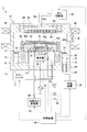
- FIG. 1 is an overall configuration diagram of a plasma processing apparatus according to an embodiment.
- the function block diagram of the control apparatus which concerns on one Embodiment. The figure for demonstrating general temperature control.
- the flowchart which showed the temperature control which concerns on one Embodiment.
- the figure for demonstrating the temperature control which concerns on one Embodiment.
- a product generated by etching a multilayer resist film and a metal-containing mask formed on the wafer during the plasma processing step of plasma etching adheres to the surface of the electrostatic chuck.
- the state of the surface of the electrostatic chuck changes and the electrostatic attraction force of the wafer decreases. Therefore, a cleaning process for cleaning the surface of the electrostatic chuck is performed while plasma processing is sequentially performed on a plurality of product wafers, and the product wafer is continuously processed while removing products on the surface of the electrostatic chuck. ing.
- the product attached to the surface of the electrostatic chuck can be efficiently removed when the temperature of the electrostatic chuck is controlled to a high temperature using the high-speed temperature control mechanism using the heater.
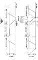
- FIG. 3 shows a general example of the set temperature of each step of the plasma processing apparatus in which the set temperature can be changed for each step in the plasma etching process in which the wafer is processed in two steps.
- the set temperature at the time of loading and unloading of the product wafer and the set temperatures of Step 1 and Step 2 during the etching process are set in advance.
- a wafer-less cleaning recipe (WLDC: Wafer-Less Dry Etching) shows a set temperature during loading and unloading and a set temperature during the cleaning process.
- Waferless cleaning is a process in which the surface of the ESC is cleaned by executing a plasma process without a wafer in the processing chamber.
- the wafer is not carried in and out, but has a set value as a recipe for convenience.
- the execution procedure of the corresponding process is set, and the set temperature of each process is also set.
- the set temperature at the time of carrying in and carrying out is the same in any recipe.
- the temperature is controlled to reach the set temperature of 20 ° C. in step 1 before the etching process of the first wafer, and a temperature stabilization waiting time occurs.
- the etching process of step 1 is executed, and then the temperature is controlled so as to reach the set temperature of 60 ° C. of step 2.
- a temperature stabilization waiting time is generated again. The etching process is executed.
- the wafer is unloaded.
- the temperature is controlled so that the set temperature at the time of unloading set in the WLDC recipe indicating the execution procedure of the next process is 50 ° C.
- a temperature stabilization waiting time also occurs.
- the cleaning process is executed.
- the set temperature 50 ° C. of the cleaning process is higher than the set temperature 20 ° C. of step 1 of the etching process.
- the set temperature is changed from 60 ° C. to 50 ° C.
- the set temperature changes from 50 ° C. to 20 ° C. when the process is changed from the cleaning process to the etching process.
- a temperature stabilization waiting time is generated each time the set temperature changes.
- the larger the temperature difference the longer the temperature stabilization wait time.
- the temperature stabilization waiting time is the time of the slanted portion in FIG. 3, and the process processing is performed when the set temperature differs between the preceding and subsequent processes due to reasons such as increasing the set temperature during the cleaning process. Temperature stabilization waiting time frequently occurs before, the throughput deteriorates and the productivity decreases.
- the temperature stabilization indicated by A and B in the temperature stabilization waiting time which is slanted in FIG. Optimize temperature setting control to reduce waiting time.
- the plasma processing apparatus 1 shown in FIG. 1 is an example of a plasma processing apparatus that can change a set temperature for each step in a plasma process that processes an object to be processed by a plurality of steps.
- the plasma processing apparatus 1 is configured as an RIE type plasma processing apparatus, and has a cylindrical chamber (processing vessel 10) made of metal such as aluminum or stainless steel.
- the processing container 10 is grounded. In the processing container 10, a plasma process such as an etching process is performed on the object to be processed.
- a mounting table 12 for mounting a semiconductor wafer W (hereinafter referred to as a wafer W) as an object to be processed is provided.
- the wafer W is subjected to fine processing such as etching by the action of plasma.
- the mounting table 12 is made of, for example, aluminum, and is supported by a cylindrical support portion 16 that extends vertically upward from the bottom of the processing container 10 via an insulating cylindrical holding portion 14.
- a focus ring 18 made of quartz, for example, surrounding the upper surface of the mounting table 12 in an annular shape is disposed.
- An exhaust path 20 is formed between the side wall of the processing vessel 10 and the cylindrical support portion 16.
- An annular baffle plate 22 is attached to the exhaust path 20.
- An exhaust port 24 is provided at the bottom of the exhaust path 20 and is connected to an exhaust device 28 via an exhaust pipe 26.
- the exhaust device 28 has a vacuum pump (not shown) and depressurizes the processing space in the processing container 10 to a predetermined degree of vacuum.
- a transfer gate valve 30 for opening and closing the loading / unloading port for the wafer W is attached to the side wall of the processing container 10.
- a high-frequency power source 32 for generating plasma is electrically connected to the mounting table 12 via a matching unit 34 and a power feed rod 36.
- the high frequency power supply 32 applies, for example, high frequency power of 60 MHz to the mounting table 12.
- the mounting table 12 also functions as a lower electrode.
- a shower head 38 which will be described later, is provided on the ceiling portion of the processing container 10 as an upper electrode having a ground potential.
- the high-frequency power source 32 is an example of a plasma source that supplies power for generating plasma and generates plasma from gas in the processing vessel 10.
- An electrostatic chuck 40 is provided on the top surface of the mounting table 12 for holding the wafer W with electrostatic attraction.
- the electrostatic chuck 40 is obtained by sandwiching an electrode 40a made of a conductive film between a pair of insulating films 40b and 40c.
- a DC power source 42 is electrically connected to the electrode 40 a via a switch 43.
- the electrostatic chuck 40 attracts and holds the wafer W on the chuck with a Coulomb force by a DC voltage from the DC power supply 42.
- the heat transfer gas supply source 52 supplies a heat transfer gas such as He gas between the upper surface of the electrostatic chuck 40 and the back surface of the wafer W through the gas supply line 54.
- the shower head 38 at the ceiling includes an electrode plate 56 having a large number of gas vent holes 56a, and an electrode support 58 that detachably supports the electrode plate 56.
- a buffer chamber 60 is provided inside the electrode support 58, and a gas supply pipe 64 connected to a gas supply source 62 is connected to a gas inlet 60 a of the buffer chamber 60. Thereby, a desired gas is supplied from the gas supply source 62 into the processing container 10.
- a magnet 66 extending annularly or concentrically is disposed around the processing vessel 10.
- a vertical RF field is formed by the high frequency power supply 32 in the plasma generation space between the shower head 38 and the mounting table 12. Due to the high frequency discharge, high density plasma is generated near the surface of the mounting table 12.
- a refrigerant pipe 70 is provided inside the mounting table 12.
- a refrigerant having a predetermined temperature is circulated and supplied to the refrigerant pipe 70 from the chiller unit 71 through the pipes 72 and 73.
- a heater 75 is embedded in the mounting table 12.
- a desired AC voltage is applied to the heater 75 from an AC power source (not shown).
- the processing temperature of the wafer W on the electrostatic chuck 40 is adjusted to a desired temperature by cooling by the chiller unit 71 and heating by the heater 75.
- These temperature controls are executed in accordance with instructions from the control device 80.
- the heater 75 may be divided into two zones, ie, the central portion and the peripheral portion of the electrostatic chuck 40, and the temperature may be controlled for each zone. According to this, temperature control with higher accuracy is possible.
- the control device 80 includes various parts attached to the plasma processing apparatus 1, such as an exhaust device 28, a high frequency power supply 32, an electrostatic chuck switch 43, a matching unit 34, a heat transfer gas supply source 52, a gas supply source 62, and a chiller unit. 71 and the heater in the electrostatic chuck 40 are controlled.
- the control device 80 is also connected to a host computer (not shown).
- the control device 80 has a CPU (Central Processing Unit), a ROM (Read Only Memory), and a RAM (Random Access Memory) (not shown).
- the CPU processes, for example, according to various recipes stored in the storage unit 85 shown in FIG. Execute.
- the recipe includes process time, process chamber temperature (upper electrode temperature, process chamber sidewall temperature, ESC temperature, etc.), pressure, applied high-frequency power, various process gas flow rates, etc., which are control information of the apparatus for a multi-step process condition.
- process control related to temperature control will be mainly described as a recipe and described below.
- the storage unit 85 in which the recipe is stored can be realized as a RAM or a ROM using, for example, a semiconductor memory, a magnetic disk, or an optical disk.
- the recipe may be provided by being stored in a storage medium and read into the storage unit 85 via a driver (not shown), or may be downloaded from a network (not shown) and stored in the storage unit 85. May be. Further, a DSP (Digital Signal Processor) may be used instead of the CPU in order to realize the functions of the above-described units.
- the function of the control device 80 may be realized by operating using software, or may be realized by operating using hardware.
- the gate valve 30 is first opened and the wafer W held on the transfer arm is loaded into the processing container 10.
- the wafer W is lifted from the transfer arm by pusher pins (not shown) protruding from the surface of the electrostatic chuck 40, and the wafer W is held on the pusher pins.
- the pusher pin is lowered into the electrostatic chuck 40, so that the wafer W is placed on the electrostatic chuck 40.
- the gate valve 30 is closed, an etching gas is introduced from the gas supply source 62 into the processing container 10 at a predetermined flow rate and flow rate ratio, and the pressure in the processing container 10 is reduced to a set value by the exhaust device 28. To do. Further, high frequency power having a predetermined power is supplied from the high frequency power supply 32 to the mounting table 12. Further, a DC voltage is applied from the DC power source 42 to the electrode 40 a of the electrostatic chuck 40 to fix the wafer W on the electrostatic chuck 40.
- the etching gas introduced in a shower form from the shower head 38 is turned into plasma by the high-frequency power from the high-frequency power source 32, thereby generating plasma between the upper electrode (shower head 38) and the lower electrode (mounting table 12). Plasma is generated in the space.
- the main surface of the wafer W is etched by radicals and ions in the generated plasma.
- the wafer W is lifted and held by the pusher pin, the gate valve 30 is opened and the transfer arm is loaded into the processing chamber 10, and then the pusher pin is lowered and the wafer W is held on the transfer arm. The Next, the transfer arm goes out of the processing container 10, and the next wafer W is loaded into the processing chamber 10 by the transfer arm. By repeating this process, the wafer W is continuously processed.
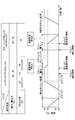
- FIG. 2 is a functional configuration diagram of the control device 80.
- the control device 80 includes a transfer control unit 81, a process execution unit 82, a storage unit 85, and a temperature control unit 86.
- the transfer control unit 81 performs a loading process for loading the wafer W into the processing container 10 of the plasma processing apparatus 1 and a unloading process for unloading the wafer W from the processing container 10.
- the carrying-in process refers to the loading of the wafer W from the gate valve 30 in a state where the wafer W is held by the transfer arm after the gate valve 30 provided in the processing container 10 is opened, and protrudes from the surface of the electrostatic chuck 40.
- the wafer W is lifted from the transfer arm by the pushed pusher pin, and the wafer W is held on the pusher pin.
- the pusher pin is lowered into the electrostatic chuck, whereby the wafer W Until it is placed on the electrostatic chuck 40.
- the wafer W is lifted and held by the pusher pin, the gate valve 30 is opened and the transfer arm is loaded into the processing chamber 10, and then the pusher pin is lowered and the wafer W is moved. The process is held until the transfer arm is held out of the processing container 10.
- the storage unit 85 stores in advance a plurality of recipes for executing an etching process and a WLDC recipe for executing a wafer rescreening process.
- the process execution unit 82 includes an etching execution unit 83 and a cleaning execution unit 84.
- the etching execution unit 83 executes a plasma etching process including a plurality of steps.
- the etching execution unit 83 selects a desired process recipe from among a plurality of process recipes stored in the storage unit 85, and executes an etching process according to the recipe.
- the cleaning execution unit 84 executes a cleaning process according to the WLDC recipe stored in the storage unit 85.
- the temperature controller 86 controls the temperature of the electrostatic chuck 40 provided in the processing container 10.
- the temperature control unit 86 performs first temperature control for controlling the set temperature of the next process in accordance with the end timing of the executed etching process, or the next process in parallel with the carry-in process or the carry-out process. At least one of the second temperature control to control to the set temperature is performed.
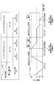
- FIG. 4 is a flowchart showing temperature control processing of the electrostatic chuck 40 (wafer W) using the control device 80 according to the present embodiment.
- the variable n indicating the number of steps is initially set to “1” in advance before this processing is started. Further, before the start of this process, the processing chamber is set to a set temperature of 20 ° C. when the etching process recipe is loaded as shown in the upper table of FIG.
- the transfer control unit 81 starts a wafer W transfer process (step S500).
- the transfer control unit 81 determines whether the wafer W has been transferred from the gate valve 30 (step S505).
- the etching execution unit 83 executes the etching process of Step 1 (Step S510). Thereby, as shown in the lower graph of FIG. 5, the etching process of step 1 of the first wafer is executed.
- the etching execution unit 83 determines whether or not this step or the entire process including this step is completed (step S515).
- the temperature control unit 86 determines whether there is a change in the set temperature of the next step of the etching process recipe (step S520).
- the temperature control unit 86 controls to the set temperature of the next step (step S525) and waits without starting the next process until the temperature becomes stable (step S530).
- the etching execution unit 83 increases the number of steps n by 1 (step S535), returns to step S510, and executes the etching process of step 2.
- the temperature rises after the processing of step 1 of the first wafer and waits for temperature stabilization until it reaches 60 ° C. After the temperature reaches 60 ° C. and stabilizes, An etching process is being performed.
- step S515 the temperature control unit 86 immediately moves to step S535 and increments the number of steps by one, and then proceeds to step S510.
- step 2 the etching process of step 2 is executed. In this way, the etching process (steps S510 to S535) is repeated until the final step.
- the temperature control unit 86 controls the temperature to the set temperature of the next recipe indicating the execution procedure of the next process, and the conveyance control.
- the unit 81 performs a wafer unloading process (step S540).
- the next process is waferless dry cleaning (WLDC)
- the wafer loading process is not performed after the wafer unloading process.
- the temperature is changed to the set temperature of the next recipe in parallel with the wafer carry-out process.
- the temperature control unit 86 pre-reads the set temperature of the next recipe and immediately after the end of the immediately preceding process, the set temperature of the next recipe is displayed in parallel with the wafer unloading process. In the graph of FIG. The temperature is controlled to a set temperature of 50 ° C. when the recipe is carried out. Thereby, the temperature stabilization waiting time can be shortened.
- the process execution unit 82 executes the process according to the type of the next process (step S550). To do.
- the next process is waferless dry cleaning WLDC. Therefore, the cleaning execution unit 84 of the process execution unit 82 executes waferless dry cleaning (step S555).
- step S565 the temperature control unit 86 sets the temperature at the time of carrying out the cleaning recipe, that is, the set temperature of the first step of the next recipe (20 ° C. in the graph of FIG. 5). Is pre-read and temperature control is performed (temperature pre-read control; an example of first temperature control).
- the transfer control unit 81 performs a wafer carry-in process in parallel (parallel processing of temperature control and transfer control; an example of second temperature control).
- the previous process is waferless dry cleaning, the wafer unloading process is not performed, and only the second wafer W loading process is performed. Therefore, since the temperature control of the next recipe and the wafer carry-in process are performed in parallel, the temperature stabilization waiting time can be shortened.
- step S570 When the temperature of the electrostatic chuck reaches 20 ° C. which is the set temperature of the next process and is stabilized and the unloading of the wafer is finished (step S570), the etching execution unit 83 of the process execution unit 82 sets the step number to 1. (Step S575), the process returns to step S510, and the etching process of step 1 of the second wafer W is executed.
- step S550 Even when it is determined in step S550 that the type of the next process is an etching process, the etching execution unit 83 sets the step number to 1 (step S580), and returns to step S510 to return to the second wafer. The etching process of W is executed.
- the temperature stabilization waiting time of the electrostatic chuck of the plasma processing apparatus 1 is shortened, so that the temperature of the wafer W can be adjusted to a desired temperature at high speed.
- the set temperature at the time of loading and unloading can be set to different temperatures, and the temperature at the time of the cleaning process is controlled to be higher than the temperature at the time of the etching process.
- the reactant deposited on the electric chuck 40 can be effectively removed.
- the temperature stabilization waiting time of the cleaning process can be shortened by pre-reading and controlling the set temperature of the next recipe at the end of one process. Furthermore, the temperature stabilization waiting time before carrying out or carrying in the wafer can also be shortened by performing the carry-in process and the carry-out process of the wafer W in parallel with the temperature stabilization wait by the pre-reading control of the set temperature.
- the temperature control method according to the present embodiment can greatly reduce the temperature stabilization waiting time as compared with a general temperature control method. As a result, throughput during wafer processing can be increased and productivity can be increased.
- Temperature control variations Here, variations of the temperature control timing will be described.
- the temperature setting for the cleaning process and the unloading of the wafer are started almost simultaneously at the end of one process.
- the temperature setting for the etching process of the second wafer W and the wafer loading are started almost simultaneously.
- the temperature control of the present embodiment in which the set temperature of the next recipe is prefetched at the end of one process is the first temperature control that controls the set temperature of the next process according to the timing of the end of the executed plasma process. It is an example, and the timing of the first temperature control for prefetching the set temperature of the next recipe is not limited to the time when one process is completed.
- the timing of the first temperature control may be within a predetermined time in conjunction with the end of one process, or may be during a wafer unloading process performed after the end of one process, It may be during the wafer carry-in process performed after the end of one process.
- the longer the elapsed time from the end of one process to the start of the first temperature control the longer the temperature stabilization wait time, and the effect of this embodiment is reduced.
- the temperature control of this embodiment in which the temperature control (waiting for temperature stabilization) and the wafer unloading process are performed in parallel is the second temperature control for controlling to the set temperature of the next process in parallel with the loading process or the unloading process.
- the start timing of the parallel processing of the wafer carry-in or carry-out process and the second temperature control is not limited to the end of one process.
- the timing of the second temperature control may be during either the wafer loading or unloading process. If the two processes are partially parallel, the one of the processes may be performed in parallel. It does not have to be included in any one of the other processes.
- the set temperature of the next process controlled by the temperature controller 86 in the first and second temperature control is the same as the set temperature of the next process in advance as the set temperature at the time of carrying out the wafer of the recipe being executed.
- the temperature control unit 86 can perform the first and second temperature control using the set temperature at the time of carrying out the wafer of the recipe being executed as the set temperature of the next process.
- the temperature control unit 86 sets the set temperature at the time of next wafer transfer to the next process.
- the first and second temperature control can be performed using the temperature.
- the temperature control unit 86 may pre-control the temperature of the set temperature of the next process set by the operator or the like. it can.
- the solid line temperature transition in the upper part of FIG. 6 indicates the result of executing the temperature control according to the present embodiment
- the solid line temperature transition in the lower part of FIG. 6 indicates the result of executing the above-described general temperature control.
- the temperature transition of the broken line in the lower part of FIG. 6 shows the temperature transition of the present embodiment in the upper part of FIG. 6 by a broken line for comparison of the temperature stabilization waiting time.
- the temperature of the electrostatic chuck is controlled to a set temperature at the time of wafer loading before the wafer is loaded, and the temperature is stable. In this state, the wafer carry-in process is started (lower stage in FIG. 6, time t1). After completion of the wafer carry-in process (time t2), the temperature is controlled to the set temperature of the second wafer process, and after the temperature is stabilized, the next process is started (time t3).
- the wafer carry-in process cannot be started until the temperature of the electrostatic chuck is controlled to the set temperature at the time of carrying the wafer. Therefore, in the temperature control according to the present embodiment, as shown in the upper part of FIG. 6, temperature monitoring during wafer loading is not performed. In this embodiment, temperature monitoring is started after the wafer carry-in process is completed. Thereby, the wafer carry-in process and the temperature control (temperature stabilization wait) can be processed in parallel. Comparing the upper and lower time charts of FIG. 6, in the temperature system according to the present embodiment, the temperature stabilization waiting time is shortened compared to general temperature control, and the start time of the second wafer processing is shortened. It can be visually understood that the throughput is improved.
- the temperature control according to the present embodiment has been described above by taking as an example the case where the etching process of the first wafer ⁇ the cleaning process ⁇ the etching process of the second wafer is performed.
- the temperature control according to the present embodiment will be described below by taking as an example a case where the etching process of the first wafer ⁇ the etching process of the second wafer is performed.
- a plasma processing apparatus that can change the set temperature for each step in a plasma process that processes a wafer by a plurality of steps is premised on a process that requires high-speed temperature control.
- the upper table in FIG. 7 shows the first etching process recipe 1 and the second etching process recipe 1 when the second wafer etching process is performed immediately after the first wafer etching process. Has been.
- the graph in the lower part of FIG. 7 shows the temperature control result of this embodiment when the second wafer is etched immediately after the first wafer is etched.
- the temperature in the processing container 10 is controlled to a set temperature of 20 ° C. when the process recipe is loaded as shown in the upper table of FIG.
- the transfer control unit 81 starts control of the wafer W loading process.
- the etching execution unit 83 performs the etching process of Step 1 on the first wafer W.
- the temperature is maintained at 20 ° C.
- the temperature control unit 86 controls the temperature to the set temperature of 60 ° C. in step 2 according to the recipe 1, and waits until the inside of the processing container 10 is stabilized at the set temperature.
- the etching execution unit 83 executes the etching process of Step 2. During the etching process of step 2 of the first wafer, the temperature is maintained at 60 ° C.
- the temperature control unit 86 changes the set temperature to execute the next process, and the transfer control unit 81 performs the wafer unloading process in parallel. Specifically, the temperature control unit 86 controls the temperature by changing the temperature setting to the set temperature of 40 ° C. when the recipe 1 is carried out.
- the set temperature is changed to the set temperature of 40 ° C. of step 1 of recipe 2 as the first wafer is carried out, and the temperature is stabilized. Until then, the temperature is controlled in parallel with the wafer unloading and loading steps.
- the temperature stabilization waiting time can be shortened by pre-reading the set temperature of the next recipe and controlling to the set temperature of the next process immediately after the end of one process.
- the temperature stabilization waiting time can also be shortened by performing the temperature control and the wafer unloading and loading processes in parallel. As a result, the throughput at the time of wafer manufacture can be increased and the productivity can be increased.
- the set temperature of the final step of the process at the end timing of the executed plasma process may be different from the set temperature of the first step of the next process. Also in this case, the temperature stabilization waiting time can be shortened and the throughput at the time of wafer manufacture can be increased.
- the temperature control For example, according to the temperature control according to the present invention, at least one of the first temperature control (preset read control of the set temperature) or the second temperature control (parallel processing of wafer loading or unloading and temperature control) is executed. Just do it. However, when both the first temperature control and the second temperature control are executed, there is a high possibility that the temperature stabilization waiting time can be shortened compared with the case where either one is executed, which can further contribute to an improvement in throughput. . In particular, when the set temperatures of the wafer carry-in process and the carry-out process are different, it is preferable to execute both the first temperature control and the second temperature control.
- the temperature control according to the present invention can be used not only for waferless dry cleaning and plasma processing of product wafers, but also for dry cleaning using wafers and plasma processes using dummy wafers.
- the temperature control according to the present invention has been described in the case where the set temperature is different between the process of the wafer after the process processing and the next wafer process, it is not limited thereto.
- the first temperature control or the first temperature control of the processing chamber is performed in parallel with the wafer loading process in order to process the first wafer from the idle state. 2 temperature control may be performed.
- the first temperature control or the second temperature control may be performed at the timing of lot switching.
- the plasma process capable of controlling the temperature according to the present invention is not limited to the etching process, and any process such as film formation, ashing, and sputtering may be used.
- the temperature control method according to the present invention can be used not only for electrostatic chucks in plasma processing apparatuses but also for temperature control of upper electrodes, deposition shields, processing containers, and the like.
- the temperature control method according to the present invention is not limited to a parallel plate type etching processing apparatus, but also a cylindrical RLSA (Radial Line Slot Antenna) plasma processing apparatus, an ICP (Inductively Coupled Plasma) plasma processing apparatus, and a microwave plasma processing. It can be used for any plasma processing apparatus such as an apparatus.
Landscapes
- Engineering & Computer Science (AREA)
- Physics & Mathematics (AREA)
- Chemical & Material Sciences (AREA)
- General Physics & Mathematics (AREA)
- Manufacturing & Machinery (AREA)
- Condensed Matter Physics & Semiconductors (AREA)
- Computer Hardware Design (AREA)
- Microelectronics & Electronic Packaging (AREA)
- Power Engineering (AREA)
- Plasma & Fusion (AREA)
- Automation & Control Theory (AREA)
- Analytical Chemistry (AREA)
- Chemical Kinetics & Catalysis (AREA)
- General Chemical & Material Sciences (AREA)
- Materials Engineering (AREA)
- Mechanical Engineering (AREA)
- Metallurgy (AREA)
- Organic Chemistry (AREA)
- Drying Of Semiconductors (AREA)
- Container, Conveyance, Adherence, Positioning, Of Wafer (AREA)
- Chemical Vapour Deposition (AREA)
Abstract
Description
近年、複数のステップによりウエハを処理するプラズマプロセスにおいてステップ毎に設定温度を変えることが可能な機構を備えたプラズマ処理装置が提案されている。このような機構には、例えば静電チャック(ESC:Electrostatic Chuck)の温度をプロセス毎又はステップ毎に高速に制御可能な高速温度制御技術として、静電チャックの表面温度をヒータにて高速に温度調整する機構が利用されている。
まず、本発明の一実施形態に係る温度制御方法を実行するプラズマ処理装置の全体構成について、図1を参照しながら説明する。
図2は、制御装置80の機能構成図である。制御装置80は、搬送制御部81、プロセス実行部82、記憶部85及び温度制御部86を有する。
図4は、本実施形態に係る制御装置80を用いた静電チャック40(ウエハW)の温度制御処理を示したフローチャートである。なお、本処理が開始される前に、ステップ数を示す変数nは予め「1」に初期設定されている。また、本処理が開始される前に処理室内は、図5の上段の表に示したエッチングプロセスレシピ搬入時の設定温度20℃に設定されている。
以上に説明した制御部80の動作により、プラズマ処理装置1の静電チャックの温度安定待ち時間が短縮されるのでウエハWの温度を高速に所望の温度に調整できる。その際、複数のステップによりウエハWを処理するプラズマプロセスにおいて搬入時と搬出時の設定温度を異なる温度に設定可能とし、エッチング処理時の温度よりクリーニング処理時の温度を高く制御することにより、静電チャック40上に堆積した反応物を効果的に除去することができる。
ここで、上記温度制御のタイミングについて、そのバリエーションを説明する。本実施形態では、クリーニング処理のための温度設定とウエハの搬出とは一のプロセスの終了時にほぼ同時に開始した。また、本実施形態では、2枚目のウエハWのエッチング処理のための温度設定とウエハの搬入とはほぼ同時に開始した。
次に、本実施形態における温度制御の監視機能について、図6を参照しながら説明する。図6上段の実線の温度推移は、本実施形態に係る温度制御を実行した結果を示し、図6下段の実線の温度推移は、上述した一般的な温度制御を実行した結果を示す。図6下段の破線の温度推移は、温度安定待ち時間の比較のために図6上段の本実施形態の温度推移を破線で示したものである。
これに対して、以下では、1枚目のウエハのエッチング処理→2枚目のウエハのエッチング処理とプロセスが実行される場合を例に挙げて、本実施形態に係る温度制御について説明する。ただし、この場合であっても、複数のステップによりウエハを処理するプラズマプロセスにおいてステップ毎に設定温度を変えることが可能なプラズマ処理装置において、高速な温度制御が要求されるプロセスが前提となる。
以上、添付図面を参照しながら本発明の好適な実施形態について詳細に説明したが、本発明はかかる例に限定されない。本発明の属する技術の分野における通常の知識を有する者であれば、特許請求の範囲に記載された技術的思想の範疇において、各種の変更例または修正例に想到し得ることは明らかであり、これらについても、当然に本発明の技術的範囲に属するものと了解される。
10 処理容器
12 載置台(下部電極)
32 高周波電源
38 シャワーヘッド(上部電極)
40 静電チャック
62 ガス供給源
71 チラーユニット
75 ヒ-タ
80 制御装置
81 搬送制御部
82 プロセス実行部
83 エッチング実行部
84 クリーニング実行部
85 記憶部
86 温度制御部
Claims (11)
- 複数のステップにより被処理体を処理するプラズマプロセスにおいてステップ毎に設定温度を変えることが可能なプラズマ処理装置の温度制御方法であって、
前記プラズマ処理装置の処理容器内へ被処理体を搬入する搬入工程又は被処理体を搬出する搬出工程の少なくともいずれかを行う搬送工程と、
前記複数のステップからなるプラズマプロセスを実行するプロセス実行工程と、
前記実行されたプラズマプロセスの終了のタイミングに応じて次のプロセスの設定温度に制御する第1の温度制御、又は前記搬入工程或いは前記搬出工程に並行して前記次のプロセスの設定温度に制御する第2の温度制御、の少なくともいずれかを行う温度制御工程と、
を含むことを特徴とする温度制御方法。 - 前記温度制御工程では、前記実行されたプラズマプロセスの終了のタイミングにおけるプロセスの最終ステップの設定温度と、次のプロセスの最初のステップの設定温度とが異なっていることを特徴とする請求項1に記載の温度制御方法。
- 前記搬入工程は、前記処理容器内に設けられた搬送用のゲートバルブが開口してから、搬送アーム上に保持された被処理体が前記処理容器内に搬入され、プッシャーピンにより保持されてから該処理容器内の載置台上に載置されるまでであることを特徴とする請求項1に記載の温度制御方法。
- 前記搬出工程は、前記プラズマプロセス実行後に被処理体がプッシャーピンにより保持されてから、搬送アーム上に保持され、前記搬送用のゲートバルブから搬出されるまでであることを特徴とする請求項1に記載の温度制御方法。
- 前記搬入工程と前記搬出工程の設定温度が異なる場合、前記第1の温度制御及び前記第2の温度制御を行うことを特徴とする請求項1に記載の温度制御方法。
- 前記温度制御工程は、前記第1の温度制御を行う場合、一のプラズマプロセスの終了とともに前記次のプロセスの設定温度に制御することを特徴とする請求項1に記載の温度制御方法。
- 前記温度制御工程は、前記第2の温度制御を行う場合、前記被処理体の搬出又は搬入とともに前記次のプロセスの設定温度に制御することを特徴とする請求項1に記載の温度制御方法。
- 前記温度制御工程では、前記次のプロセスの設定温度は、複数のステップからなる前記一のプラズマプロセスのいずれかのステップの設定温度より高いことを特徴とする請求項6に記載の温度制御方法。
- 前記温度制御工程は、前記搬送工程前及び前記搬送工程中に温度監視は行わず、前記搬送工程後に温度監視を開始することを特徴とする請求項1に記載の温度制御方法。
- 複数のステップにより被処理体を処理するプラズマプロセスにおいてステップ毎に設定温度を変えることが可能なプラズマ処理装置の制御装置であって、
前記プラズマ処理装置の処理容器内へ被処理体を搬入する搬入工程又は被処理体を搬出する搬出工程の少なくともいずれかを行う搬送制御部と、
前記複数のステップからなるプラズマプロセスを実行するプロセス実行部と、
前記実行されたプラズマプロセスの終了のタイミングに応じて次のプロセスの設定温度に制御する第1の温度制御、又は前記搬入工程或いは前記搬出工程に並行して前記次のプロセスの設定温度に制御する第2の温度制御、の少なくともいずれかを行う温度制御部と、
を備えることを特徴とする制御装置。 - 処理容器と、
前記処理容器内にガスを供給するガス供給源と、
プラズマを生成するためのパワーを供給し、ガスからプラズマを生成するプラズマ源と、
前記処理容器内に設けられた載置台、上部電極、デポシールド又は前記処理容器の少なくともいずれかの温度を制御する温度制御部と、
前記プラズマ処理装置の処理容器内へ被処理体を搬入する搬入工程又は被処理体を搬出する搬出工程の少なくともいずれかを行う搬送制御部と、
前記生成されたプラズマにより前記複数のステップからなるプラズマプロセスを実行するプロセス実行部と、を備え、
前記温度制御部は、
前記実行されたプラズマプロセスの終了のタイミングに応じて次のプロセスの設定温度に制御する第1の温度制御、又は前記搬入工程或いは前記搬出工程に並行して前記次のプロセスの設定温度に制御する第2の温度制御、の少なくともいずれかを行うことを特徴とするプラズマ処理装置。
Priority Applications (2)
| Application Number | Priority Date | Filing Date | Title |
|---|---|---|---|
| US14/354,649 US10254774B2 (en) | 2011-11-08 | 2012-10-30 | Temperature control method, control apparatus, and plasma processing apparatus |
| KR1020147012222A KR102015679B1 (ko) | 2011-11-08 | 2012-10-30 | 온도 제어 방법, 제어 장치 및 플라즈마 처리 장치 |
Applications Claiming Priority (4)
| Application Number | Priority Date | Filing Date | Title |
|---|---|---|---|
| JP2011-244539 | 2011-11-08 | ||
| JP2011244539A JP5933222B2 (ja) | 2011-11-08 | 2011-11-08 | 温度制御方法、制御装置及びプラズマ処理装置 |
| US201161560952P | 2011-11-17 | 2011-11-17 | |
| US61/560,952 | 2011-11-17 |
Publications (1)
| Publication Number | Publication Date |
|---|---|
| WO2013069510A1 true WO2013069510A1 (ja) | 2013-05-16 |
Family
ID=48289888
Family Applications (1)
| Application Number | Title | Priority Date | Filing Date |
|---|---|---|---|
| PCT/JP2012/078077 WO2013069510A1 (ja) | 2011-11-08 | 2012-10-30 | 温度制御方法、制御装置及びプラズマ処理装置 |
Country Status (5)
| Country | Link |
|---|---|
| US (1) | US10254774B2 (ja) |
| JP (1) | JP5933222B2 (ja) |
| KR (1) | KR102015679B1 (ja) |
| TW (1) | TWI557797B (ja) |
| WO (1) | WO2013069510A1 (ja) |
Families Citing this family (6)
| Publication number | Priority date | Publication date | Assignee | Title |
|---|---|---|---|---|
| JP6159172B2 (ja) * | 2013-06-26 | 2017-07-05 | 東京エレクトロン株式会社 | 温度制御方法及びプラズマ処理装置 |
| JP6287018B2 (ja) * | 2013-10-04 | 2018-03-07 | 富士通株式会社 | 可視化方法、表示方法、情報処理装置、可視化プログラム及び表示プログラム |
| WO2020031224A1 (ja) * | 2018-08-06 | 2020-02-13 | 株式会社日立ハイテクノロジーズ | プラズマ処理方法およびプラズマアッシング装置 |
| JP2021042409A (ja) * | 2019-09-09 | 2021-03-18 | 東京エレクトロン株式会社 | プラズマ処理装置及び温度制御方法 |
| JP7394668B2 (ja) | 2020-03-13 | 2023-12-08 | 東京エレクトロン株式会社 | 温度制御方法およびプラズマ処理装置 |
| CN114080662A (zh) | 2020-06-16 | 2022-02-22 | 株式会社日立高新技术 | 等离子处理装置以及等离子处理方法 |
Citations (3)
| Publication number | Priority date | Publication date | Assignee | Title |
|---|---|---|---|---|
| JPH08158071A (ja) * | 1994-12-05 | 1996-06-18 | Sumitomo Metal Ind Ltd | プラズマプロセス装置 |
| JPH09260474A (ja) * | 1996-03-22 | 1997-10-03 | Sony Corp | 静電チャックおよびウエハステージ |
| JPH11345771A (ja) * | 1998-05-29 | 1999-12-14 | Hitachi Ltd | 枚葉式真空処理方法及び装置 |
Family Cites Families (14)
| Publication number | Priority date | Publication date | Assignee | Title |
|---|---|---|---|---|
| US5089441A (en) * | 1990-04-16 | 1992-02-18 | Texas Instruments Incorporated | Low-temperature in-situ dry cleaning process for semiconductor wafers |
| JPH08288230A (ja) * | 1995-04-18 | 1996-11-01 | Kokusai Electric Co Ltd | 電気炉の加熱制御装置 |
| US5589041A (en) * | 1995-06-07 | 1996-12-31 | Sony Corporation | Plasma sputter etching system with reduced particle contamination |
| JP3245369B2 (ja) * | 1996-11-20 | 2002-01-15 | 東京エレクトロン株式会社 | 被処理体を静電チャックから離脱する方法及びプラズマ処理装置 |
| JP2000021964A (ja) * | 1998-07-06 | 2000-01-21 | Ngk Insulators Ltd | 静電チャックのパーティクル発生低減方法および半導体製造装置 |
| EP1319244A1 (en) * | 2000-09-20 | 2003-06-18 | Kla-Tencor Inc. | Methods and systems for semiconductor fabrication processes |
| US6921724B2 (en) * | 2002-04-02 | 2005-07-26 | Lam Research Corporation | Variable temperature processes for tunable electrostatic chuck |
| KR100770128B1 (ko) * | 2005-07-26 | 2007-10-24 | 삼성에스디아이 주식회사 | 플라즈마 디스플레이 장치 |
| US7723648B2 (en) | 2006-09-25 | 2010-05-25 | Tokyo Electron Limited | Temperature controlled substrate holder with non-uniform insulation layer for a substrate processing system |
| US7960297B1 (en) * | 2006-12-07 | 2011-06-14 | Novellus Systems, Inc. | Load lock design for rapid wafer heating |
| US20080237184A1 (en) * | 2007-03-30 | 2008-10-02 | Mamoru Yakushiji | Method and apparatus for plasma processing |
| US8194384B2 (en) * | 2008-07-23 | 2012-06-05 | Tokyo Electron Limited | High temperature electrostatic chuck and method of using |
| JP4611409B2 (ja) * | 2008-09-03 | 2011-01-12 | 晃俊 沖野 | プラズマ温度制御装置 |
| JP6219251B2 (ja) * | 2014-09-17 | 2017-10-25 | 東芝メモリ株式会社 | 半導体製造装置 |
-
2011
- 2011-11-08 JP JP2011244539A patent/JP5933222B2/ja active Active
-
2012
- 2012-10-30 WO PCT/JP2012/078077 patent/WO2013069510A1/ja active Application Filing
- 2012-10-30 US US14/354,649 patent/US10254774B2/en active Active
- 2012-10-30 KR KR1020147012222A patent/KR102015679B1/ko active IP Right Grant
- 2012-11-01 TW TW101140597A patent/TWI557797B/zh active
Patent Citations (3)
| Publication number | Priority date | Publication date | Assignee | Title |
|---|---|---|---|---|
| JPH08158071A (ja) * | 1994-12-05 | 1996-06-18 | Sumitomo Metal Ind Ltd | プラズマプロセス装置 |
| JPH09260474A (ja) * | 1996-03-22 | 1997-10-03 | Sony Corp | 静電チャックおよびウエハステージ |
| JPH11345771A (ja) * | 1998-05-29 | 1999-12-14 | Hitachi Ltd | 枚葉式真空処理方法及び装置 |
Also Published As
| Publication number | Publication date |
|---|---|
| KR102015679B1 (ko) | 2019-08-28 |
| US10254774B2 (en) | 2019-04-09 |
| TWI557797B (zh) | 2016-11-11 |
| TW201334061A (zh) | 2013-08-16 |
| JP5933222B2 (ja) | 2016-06-08 |
| JP2013102041A (ja) | 2013-05-23 |
| US20140288726A1 (en) | 2014-09-25 |
| KR20140090180A (ko) | 2014-07-16 |
Similar Documents
| Publication | Publication Date | Title |
|---|---|---|
| JP6100672B2 (ja) | 温度制御機構、温度制御方法及び基板処理装置 | |
| WO2013069510A1 (ja) | 温度制御方法、制御装置及びプラズマ処理装置 | |
| JP2019192734A (ja) | プラズマエッチング方法及びプラズマ処理装置 | |
| KR102143272B1 (ko) | 기판 처리 장치, 기판 적재 기구, 및 기판 처리 방법 | |
| TW201543571A (zh) | 蝕刻方法 | |
| JP2015154047A (ja) | エッチング方法、及びプラズマ処理装置 | |
| TWI619164B (zh) | 用於電漿蝕刻操作的基材支撐件 | |
| US10546723B2 (en) | Plasma processing method | |
| KR20210029100A (ko) | 플라즈마 처리 장치, 처리 방법 및 상부 전극 구조 | |
| JP6159172B2 (ja) | 温度制御方法及びプラズマ処理装置 | |
| US9818582B2 (en) | Plasma processing method | |
| TWI719958B (zh) | 電漿蝕刻方法 | |
| JP7154105B2 (ja) | クリーニング方法及びプラズマ処理装置 | |
| TWI831956B (zh) | 清潔處理方法及電漿處理裝置 | |
| CN110021524B (zh) | 蚀刻方法 | |
| JP2006351814A (ja) | クリーニング方法、コンピュータプログラム及び成膜装置 | |
| JP2020205361A (ja) | プラズマ処理方法及びプラズマ処理装置 | |
| JP7382848B2 (ja) | 基板処理方法および基板処理装置 | |
| KR20210032904A (ko) | 실리콘 산화막을 에칭하는 방법 및 플라즈마 처리 장치 | |
| KR20210035073A (ko) | 플라즈마 처리 방법 및 플라즈마 처리 장치 | |
| JP2020167279A (ja) | プラズマ処理装置 | |
| JP7160291B2 (ja) | エッチング方法、及びエッチング装置 | |
| US20230298860A1 (en) | Apparatus And Method Of Treating Substrate | |
| JP2021114551A (ja) | エッチング方法及びプラズマ処理装置 | |
| JP2022027040A (ja) | プラズマ処理装置及びプラズマ処理方法 |
Legal Events
| Date | Code | Title | Description |
|---|---|---|---|
| 121 | Ep: the epo has been informed by wipo that ep was designated in this application |
Ref document number: 12848016 Country of ref document: EP Kind code of ref document: A1 |
|
| WWE | Wipo information: entry into national phase |
Ref document number: 14354649 Country of ref document: US |
|
| ENP | Entry into the national phase |
Ref document number: 20147012222 Country of ref document: KR Kind code of ref document: A |
|
| NENP | Non-entry into the national phase |
Ref country code: DE |
|
| 122 | Ep: pct application non-entry in european phase |
Ref document number: 12848016 Country of ref document: EP Kind code of ref document: A1 |