WO2013015303A1 - 光学部材 - Google Patents
光学部材 Download PDFInfo
- Publication number
- WO2013015303A1 WO2013015303A1 PCT/JP2012/068794 JP2012068794W WO2013015303A1 WO 2013015303 A1 WO2013015303 A1 WO 2013015303A1 JP 2012068794 W JP2012068794 W JP 2012068794W WO 2013015303 A1 WO2013015303 A1 WO 2013015303A1
- Authority
- WO
- WIPO (PCT)
- Prior art keywords
- refractive index
- index layer
- multilayer film
- dielectric multilayer
- optical member
- Prior art date
- Legal status (The legal status is an assumption and is not a legal conclusion. Google has not performed a legal analysis and makes no representation as to the accuracy of the status listed.)
- Ceased
Links
Images




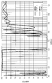

Classifications
-
- G—PHYSICS
- G02—OPTICS
- G02B—OPTICAL ELEMENTS, SYSTEMS OR APPARATUS
- G02B5/00—Optical elements other than lenses
- G02B5/20—Filters
- G02B5/28—Interference filters
- G02B5/281—Interference filters designed for the infrared light
- G02B5/282—Interference filters designed for the infrared light reflecting for infrared and transparent for visible light, e.g. heat reflectors, laser protection
-
- G—PHYSICS
- G02—OPTICS
- G02B—OPTICAL ELEMENTS, SYSTEMS OR APPARATUS
- G02B5/00—Optical elements other than lenses
- G02B5/20—Filters
- G02B5/28—Interference filters
- G02B5/285—Interference filters comprising deposited thin solid films
-
- G—PHYSICS
- G02—OPTICS
- G02B—OPTICAL ELEMENTS, SYSTEMS OR APPARATUS
- G02B5/00—Optical elements other than lenses
- G02B5/20—Filters
- G02B5/28—Interference filters
- G02B5/285—Interference filters comprising deposited thin solid films
- G02B5/286—Interference filters comprising deposited thin solid films having four or fewer layers, e.g. for achieving a colour effect
Definitions
- the present invention relates to an optical member having a dielectric multilayer film.
- An imaging device such as a digital still camera images a subject using a solid-state imaging device such as a CCD (Charge Coupled Device) or a CMOS image sensor (Complementary Metal Oxide Semiconductor Semiconductor Image Sensor).
- a solid-state imaging device such as a CCD (Charge Coupled Device) or a CMOS image sensor (Complementary Metal Oxide Semiconductor Semiconductor Image Sensor).
- CCD Charge Coupled Device
- CMOS image sensor Complementary Metal Oxide Semiconductor Semiconductor Image Sensor
- a filter used for such applications is required to have a high light transmittance in the visible wavelength range.
- a plurality of high refractive index layers and low refractive index layers are alternately stacked.
- a dielectric multilayer film is used.
- a filter having a dielectric multilayer film has an incident angle dependency of light, and when applied to an imaging device, the cutoff wavelength moves depending on the incident angle of light incident on the filter through an imaging lens.
- the color may change between the center and the periphery of the photographed image.
- incident angle dependency of light is simply referred to as incident angle dependency.
- a first dielectric multilayer film and a second dielectric multilayer film are provided, and the width of the reflection band of the first dielectric multilayer film is set to the second dielectric multilayer film.
- the position of the short wavelength side edge of the second dielectric multilayer film is between the short wavelength side edge and the long wavelength side edge of the reflection band of the first dielectric multilayer film.
- a method is known in which the average refractive index of the entire first dielectric multilayer film is made higher than the average refractive index of the entire second dielectric multilayer film.
- Patent Document 2 is such an example.
- a first selective transmission multilayer film composed of a high refractive index layer and a medium refractive index layer, and a second selective transmission multilayer composed of a high refractive index layer and a low refractive index layer having a large refractive index ratio A method of combining with a membrane is known. In such a method, the incidence angle dependency is reduced by the first selective transmission multilayer film including the high refractive index layer and the medium refractive index layer.
- Patent Document 3 is such an example.
- a method of using a high dielectric multilayer film in combination with a dielectric multilayer film having a low average refractive index composed of a high refractive index layer and a low refractive index layer is also known. It needs to be formed and is not necessarily excellent in productivity.
- the present invention has been made in order to solve the above problems, and is a dielectric multilayer in which a high refractive index layer having a refractive index of 2 or more and a low refractive index layer having a refractive index of 1.6 or less are alternately laminated.
- an object is to reduce the incident angle dependency.
- the optical member of the present invention is a unit refractive index layer formed of a transparent base, a high refractive index layer having a refractive index of 2 or more, and a low refractive index layer having a refractive index of 1.6 or less. And a dielectric multilayer film in which a plurality of layers are stacked.
- the total number of the unit refractive index layers in the dielectric multilayer film is 15 or more, and the optical film thickness of the high refractive index layer in the unit refractive index layer is n H d H ,
- the optical film thickness of the low refractive index layer is n L d L
- the number of unit refractive index layers satisfying n H d H / n L d L ⁇ 3 in the dielectric multilayer film is 10 or more. It is characterized by that.
- the optical member of the present invention has a dielectric multilayer film in which a plurality of unit refractive index layers each including a high refractive index layer having a refractive index of 2 or more and a low refractive index layer having a refractive index of 1.6 or less are laminated.
- the total number of unit refractive index layers in the dielectric multilayer film is 15 or more, and the number of unit refractive index layers in the dielectric multilayer film satisfying n H d H / n L d L ⁇ 3 By setting it to 10 or more, the incident angle dependency can be effectively reduced.
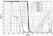
- FIG. 3 is a diagram showing the spectral transmittance of the optical member of Example 1.
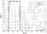
- FIG. 6 is a diagram showing the spectral transmittance of the optical member of Example 2.
- FIG. 6 is a diagram showing the spectral transmittance of the optical member of Example 3.
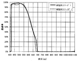
- FIG. 10 is a diagram showing the spectral transmittance of the optical member of Example 4.
- the optical member 1 of the present invention includes a transparent substrate 2 and a dielectric multilayer film 3 formed on the transparent substrate 2.
- the dielectric multilayer film 3 is formed by laminating a plurality of unit refractive index layers 33 including a high refractive index layer 31 having a refractive index of 2 or more and a low refractive index layer 32 having a refractive index of 1.6 or less.
- the refractive index means a refractive index for light having a wavelength of 550 nm.
- the optical member 1 of the present invention is characterized in that the total number of unit refractive index layers 33 in the dielectric multilayer film 3 is 15 or more. Further, when the optical film thickness of the high refractive index layer 31 in the unit refractive index layer 33 is n H d H and the optical film thickness of the low refractive index layer 32 is n L d L , n H d in the dielectric multilayer film 3 is obtained.
- the number of unit refractive index layers 33 satisfying H / n L d L ⁇ 3 is 10 or more.
- the dielectric multilayer film 3 does not necessarily need to be composed only of the unit refractive index layer 33.
- the unit refractive index layer 33 is formed in one or both of the thickness direction, that is, the stacking direction of the unit refractive index layers 33.
- the high refractive index layer 31 or the low refractive index layer 32 may be present alone.
- n H d H / n L d L may be the same or different from each other.
- such a dielectric multilayer film 3 may be referred to as a first dielectric multilayer film 3.
- the refractive index is increased by setting the number of unit refractive index layers 33 satisfying n H d H / n L d L ⁇ 3 in the dielectric multilayer film 3 to 10 or more.
- the incident angle dependency can be effectively reduced. Specifically, the difference between the 50% transmission wavelength at the incident angle of 0 ° and the 50% transmission wavelength at the incident angle of 30 ° in the cutoff band between the transmission band and the reflection band, usually in the cutoff band near 650 nm.
- the difference may be referred to as an infrared-side half-value wavelength shift amount or simply a wavelength shift amount.
- the number of the unit refractive index layers 33 satisfying n H d H / n L d L ⁇ 5 is 10 or more from the viewpoint of more effectively reducing the incident angle dependency. It is preferable.
- the number of unit refractive index layers 33 to be formed is preferably larger from the viewpoint of reducing the incident angle dependency and improving the transmittance ripple, that is, the flatness of the spectral transmittance.
- the total number of unit refractive index layers 33 in the dielectric multilayer film 3 is preferably 30 or more, and more preferably 35 or more.
- the number of unit refractive index layers 33 satisfying n H d H / n L d L ⁇ 3, preferably n H d H / n L d L ⁇ 5 in the dielectric multilayer film 3 is preferably 15 or more. 18 or more is more preferable.
- the difference between the 50% transmission wavelength at an incident angle of 0 ° and the 50% transmission wavelength at an incident angle of 30 °, particularly in the cutoff band near 650 nm, is 16 nm or less. It is easy to reduce the transmittance ripple.
- the number of unit refractive index layers 33 to be formed is preferably large from the viewpoint of shielding the infrared region, but is preferably suppressed from the viewpoint of productivity. Therefore, the total number of unit refractive index layers 33 in the dielectric multilayer film 3 is preferably 45 or less, and more preferably 40 or less.
- n H d H / n L d L ⁇ 3 in the dielectric multilayer film 3 preferably the number of layers of the n H d H / n L d L ⁇ 5 units refractive index layer 33 that satisfies is preferably 35 or less 30 or less is more preferable.
- the number of unit refractive index layers 33 satisfying 5 ⁇ n H d H / n L d L ⁇ 8 is preferably 10 or more, and more preferably 15 or more.
- the difference between the 50% transmission wavelength at the incident angle of 0 ° and the 50% transmission wavelength at the incident angle of 30 ° in the cutoff band near 650 nm is set to 16 nm or less, and the transmittance ripple is reduced. It's easy to do.
- the average n H d H / n L d L which is the average value of n H d H / n L d L in the whole of the rate layer 33 is preferably 4.5 to 6.
- the average n H d H / n L d L is preferably 4.5 to 5.3.
- n H d H / n L d L of each unit refractive index layer 33 in the dielectric multilayer film 3 is not necessarily limited as long as the above conditions are satisfied, but is preferably 0.1 to 25, more preferably 0.2 to 20. .
- n H d H / n L d L ⁇ 3 preferably n H d H / n L d L ⁇ 5. More preferably, 5 ⁇ n H d H / n L d L ⁇ 8 is satisfied.
- the average optical thickness n H d H is the average value of the optical thickness n H d H of the high refractive index layer 31 in the dielectric multilayer film 3 is preferably 200 ⁇ 310 nm, more preferably 210 ⁇ 300 nm.
- the average optical thickness n L d L is the average value of the optical thickness n L d L of the low refractive index layer 32 in the dielectric multilayer film 3 is preferably 40 ⁇ 70 nm, more preferably 40 ⁇ 65 nm.
- thickness n H d average optical thickness n H d H is the average value of H is preferably 210 ⁇ 270 nm, more preferably 220 ⁇ 260 nm.
- the average optical thickness n L d L is the average value of the optical thickness n L d L of the low refractive index layer 32 in the dielectric multilayer film 3 is preferably 45 ⁇ 70 nm, more preferably 45 ⁇ 65 nm.
- the optical film thickness n H d H of each high refractive index layer 31 in the dielectric multilayer film 3 is not necessarily limited as long as the above conditions are satisfied, but is preferably 10 to 350 nm.
- the optical film thickness n L d L of each low refractive index layer 32 in the dielectric multilayer film 3 is not necessarily limited as long as the above conditions are satisfied, but is preferably 10 to 140 nm.
- the constituent material of the high refractive index layer 31 is not necessarily limited as long as the refractive index is 2 or more, and examples thereof include TiO 2 , Nb 2 O 5 , Ta 2 O 5 , and composite oxides thereof.
- the constituent material of the low refractive index layer 32 is not necessarily limited as long as the refractive index is 1.6 or less, and examples thereof include SiO 2 , MgF 2 , and composite oxides thereof.
- the high refractive index layer 31 and the low refractive index layer 32 can contain an additive for adjusting the refractive index within a range satisfying the refractive index.
- examples include O 3 , ZnO, ZrO 2 , NiO, ITO (Indium Tin Oxide), ATO (Antimony doped Tin Oxide), and MgO.
- the high refractive index layer 31 and the low refractive index layer 32 are preferably made of a single constituent material.
- the film thickness adjusting mechanism for forming the dielectric multilayer film 3 only needs to correspond to two constituent materials, and only two types of film materials are available, so productivity in the film forming process is increased. Can be improved.
- the high refractive index layer 31 and the low refractive index layer 32 are formed by, for example, a sputtering method, a vacuum evaporation method, an ion beam method, an ion plating method, or a CVD method. According to these forming methods, each refractive index layer can be formed relatively easily while controlling the thickness of each refractive index layer with high accuracy. Further, since the sputtering method or the ion plating method is a so-called plasma atmosphere treatment, the adhesion of the dielectric multilayer film 3 to the transparent substrate 2 can be improved.
- the transparent substrate 2 may be either colorless or colored, and the shape thereof is not particularly limited as long as it transmits light in the visible wavelength range.
- a plate shape, a film shape, a block Shape, lens shape and the like For example, a plate shape, a film shape, a block Shape, lens shape and the like.
- the constituent material of the transparent substrate 2 is glass, crystal, crystal such as lithium niobate, sapphire, polyester resin such as polyethylene terephthalate (PET), polybutylene terephthalate (PBT), polyethylene, polypropylene, ethylene vinyl acetate copolymer And polyolefin resins such as norbornene resin, polyacrylate and polymethyl methacrylate, urethane resin, vinyl chloride resin, fluororesin, polycarbonate resin, polyvinyl butyral resin, and polyvinyl alcohol resin. These materials may have an absorption characteristic for at least one of the ultraviolet wavelength region and the infrared wavelength region.
- polyester resin such as polyethylene terephthalate (PET), polybutylene terephthalate (PBT), polyethylene, polypropylene, ethylene vinyl acetate copolymer
- polyolefin resins such as norbornene resin, polyacrylate and polymethyl methacrylate, urethane resin, vinyl chloride resin, fluor
- Glass can be used by appropriately selecting characteristics such as the presence or absence of an alkali component and the size of a linear expansion coefficient from a transparent material in the visible wavelength range in consideration of an apparatus to be used, a place where the glass is disposed, and the like.
- Borosilicate glass is preferable because it is easy to process and can suppress generation of scratches and foreign matters on the optical surface, and glass containing no alkali component is preferable because of good adhesion and weather resistance.
- the glass may be an absorption type glass having absorption in an infrared wavelength region in which CuO or the like is added to fluorophosphate glass or phosphate glass.
- the transparent substrate 2 preferably has absorption in the infrared wavelength region.
- the transparent substrate 2 has absorption in the infrared wavelength region, so that color correction close to human visibility characteristics can be performed.
- the dielectric multilayer film 3 is used for the purpose of complementing a portion where the transparent substrate 2 is not sufficiently absorbed. By using the dielectric multilayer film 3, spectral characteristics with low incident angle dependency can be obtained, and thus the spectral characteristics of the transparent substrate 2 are not adversely affected. Therefore, it is possible to obtain the optical member 1 having good characteristics as a near-infrared cut filter for an imaging device.
- Crystals such as quartz, lithium niobate, and sapphire are used as low-pass filters and wave plates for reducing moiré and false colors in imaging devices such as digital still cameras, digital video cameras, surveillance cameras, in-vehicle cameras, and webcams.
- the optical member 1 is provided with functions of a low-pass filter and a wave plate, and for example, the imaging device can be reduced in size and thickness.
- a cover for protecting a solid-state image sensor is hermetically attached to a solid-state image sensor or a solid-state image sensor package in the image pickup apparatus.
- this cover By using this cover as the transparent substrate 2, the infrared ray shielding function can be imparted to the cover, and the incident angle dependency can be reduced.
- the material for the cover include crystal, glass, and resin, but crystal or glass is preferable from the viewpoint of heat resistance.
- the resin is selected, a material having excellent heat resistance, for example, an organic-inorganic hybrid material containing an acrylic resin, a silicone resin, a fluororesin, silsesquioxane, or the like is preferable.
- the dielectric multilayer film 3 may include the following adjustment unit.
- the dielectric multilayer film 3 is capable of obtaining a spectral characteristic having a low incident angle dependency.
- the infrared half-value wavelength shift amount can be further reduced.
- the infrared-side half-value wavelength shift amount of the optical member 1 can be 10 nm or less.
- the adjustment unit is characterized by high dependence on the incident angle in the spectral characteristics by itself, and waveform deformation at oblique incidence. Specifically, the near-infrared-side half-wavelength waveform by the adjustment unit changes greatly with oblique incidence, resulting in a smaller wavelength shift amount near the near-infrared-side half-value wavelength due to the entire dielectric multilayer film 3. .
- the waveform shift near the half-infrared wavelength near the infrared side due to the dielectric multilayer film 3 other than the adjustment unit shifts in parallel in a similar shape with oblique incidence, but the waveform shift by the adjustment unit is accompanied by waveform deformation, that is, not in a similar shape. shift.
- the wavelength shift amount is basically small, and the wavelength shift amount of the near-infrared half-value wavelength can be extremely reduced by utilizing waveform deformation. It should be noted that such waveform deformation at the time of oblique incidence of the adjusting portion is caused by a change in the optical film thickness accompanying a change in the incident angle.
- the adjustment unit is composed of at least a part of a high refractive index layer 31 having a refractive index of 2 or more and a low refractive index layer 32 having a refractive index of 1.6 or less in the dielectric multilayer film 3.
- refractive index layer 31 and the total number of layers and the low refractive index layer 32 is 10 or more layers, and the average optical thickness of T H of the high refractive index layer 31, and an average optical thickness of the low refractive index layer 32 T L
- T H / T L is 1.5 or less, it is preferable. By setting it as such, it can be set as the above-mentioned spectral characteristics.
- the average optical film thickness TL of the low refractive index layer 32 is obtained by dividing the total optical film thickness of the low refractive index layer 32 constituting the adjustment unit by the number of layers of the low refractive index layer 32 constituting the adjustment unit. It is a thing.
- the adjustment part does not necessarily need to be continuously formed of 10 layers or more, and may be formed by being divided into two or more parts. When formed in a divided manner, the number of layers in at least one portion is preferably 10 or more. In the case of being divided and formed, it is not always necessary that T H / T L is 1.5 or less for each part, and T H / T L is 1. It only needs to be 5 or less.
- the total number of layers in the adjustment unit is preferably as the fundamental number increases because it becomes easier to obtain the predetermined spectral characteristics, but is preferably 100 layers or less and more preferably 50 layers or less from the viewpoint of productivity.
- T H / TL is not necessarily limited as long as it is 1.5 or less, but is preferably 1.0 or less and more preferably 0.9 or less because predetermined spectral characteristics are easily obtained.
- T H / T L is usually preferably 0.1 or more, and more preferably 0.3 or more.
- the average wavelength shift amount at a transmittance of 1 to 95% in the infrared cut-off region with and without using the adjusting portion in the dielectric multilayer film 3 is almost the same. This is presumably because the influence on the waveform shift at oblique incidence in the dielectric multilayer film 3 is dominated by the spectral characteristics due to the configuration of the dielectric multilayer film 3 other than the adjustment section.
- the adjustment unit can be used to reduce the waveform shift in the region where the transmittance exceeds 50%, and thereby the incident angle in the red wavelength range. Since the dependency can be reduced, it is possible to contribute to image improvement in the imaging apparatus.
- the optical member 1 having the adjusting portion has the following spectral characteristics. That is, it is preferable that the shift amount in the wavelength region where the near-infrared transmittance is 50% to 90% when the incident angle ⁇ is changed from 0 ° to 30 ° is 10 nm or less. Thereby, the wavelength shift of the red wavelength range (near 630 nm) is suppressed, which can contribute to image improvement in the imaging apparatus.
- the near-infrared half-value wavelength is preferably in the range of 600 to 700 nm and more preferably in the range of 620 to 680 nm when the incident angle ⁇ is 0 °.
- the optical member 1 has a transparent substrate 2 on the side opposite to the main surface on which the first dielectric multilayer film 3 is provided, as shown in FIG.
- a second dielectric multilayer film 4 can be provided on the main surface to shield the longer wavelength region of the ultraviolet wavelength region and the infrared wavelength region.
- a plurality of unit refractive index layers 43 each including a high refractive index layer 41 having a refractive index of 2 or more and a low refractive index layer 42 having a refractive index of 1.6 or less are stacked.
- the total number of unit refractive index layers 43 in the second dielectric multilayer film 4 is preferably 3 or more, and more preferably 4 or more, from the viewpoint of effectively shielding light in the ultraviolet wavelength region and infrared wavelength region.
- the total number of unit refractive index layers 43 in the second dielectric multilayer film 4 is preferably 55 or less, more preferably 50 or less, from the viewpoint of productivity and the like.
- n H d H / n L d L which is an average value of n H d H / n L d L of the entire unit refractive index layer 43 in the second dielectric multilayer film 4 is 0.8 to 1.5. Is preferable, and 0.9 to 1.4 is more preferable.
- the n H d H / n L d L value of each unit refractive index layer 43 in the second dielectric multilayer film 4 is not necessarily limited as long as the above conditions are satisfied, but is preferably 0.1 to 10, 1 to 8 are preferred.
- the average optical thickness n H d H is the average value of the optical thickness n H d H of the high refractive index layer 41 of the second dielectric multilayer film 4 is preferably 100 ⁇ 250 nm, more preferably 120 ⁇ 230 nm.
- the average optical thickness n L d L is the average value of the optical thickness n L d L of the low refractive index layer 42 of the second dielectric multilayer film 4 is preferably 100 ⁇ 230nm, 120 ⁇ 210nm Gayori preferable.
- the optical film thickness n H d H of each high refractive index layer 41 in the second dielectric multilayer film 4 is not necessarily limited as long as the above conditions are satisfied, but is preferably 10 to 310 nm, and more preferably 15 to 300 nm.
- the optical film thickness n L d L of each low refractive index layer 42 in the second dielectric multilayer film 4 is not necessarily limited as long as the above conditions are satisfied, but is preferably 5 to 310 nm, and more preferably 10 to 300 nm.
- the constituent material of the high refractive index layer 41 is not necessarily limited as long as the refractive index is 2 or more. Examples thereof include TiO 2 , Nb 2 O 5 , Ta 2 O 5 , and composite oxides thereof.
- the constituent material of the low refractive index layer 42 is not necessarily limited as long as the refractive index is 1.6 or less, and examples thereof include SiO 2 , MgF 2 , and composite oxides thereof.
- the high refractive index layer 41 and the low refractive index layer 42 can contain an additive for adjusting the refractive index within a range satisfying the refractive index.
- examples include O 3 , ZnO, ZrO 2 , NiO, ITO (Indium Tin Oxide), ATO (Antimony doped Tin Oxide), and MgO.
- the high refractive index layer 41 and the low refractive index layer 42 are formed by, for example, a sputtering method, a vacuum evaporation method, an ion beam method, an ion plating method, or a CVD method. According to these forming methods, each refractive index layer can be formed relatively easily while controlling the thickness of each refractive index layer with high accuracy. Further, since the sputtering method or the ion plating method is a so-called plasma atmosphere treatment, the adhesion of the second dielectric multilayer film 4 to the transparent substrate 2 can be improved.
- the optical member 1 has a difference between a 50% transmission wavelength at an incident angle of 0 ° and a 50% transmission wavelength at an incident angle of 30 ° in a cutoff band between a transmission band and a reflection band, usually in a cutoff band near 650 nm. Is preferably 20 nm or less, and more preferably 18 nm or less.
- the layer of the unit refractive index layer 33 that satisfies n H d H / n L d L ⁇ 3, preferably n H d H / n L d L ⁇ 5, in the first dielectric multilayer film 3.
- the number By setting the number to 10 or more, more preferably 15 or more, and even more preferably 18 or more, for example, the difference between the 50% transmission wavelength at an incident angle of 0 ° and the 50% transmission wavelength at an incident angle of 30 ° is reduced to 16 nm or less. You can also.
- the optical member 1 is used as, for example, a near-infrared cut filter such as a digital still camera, a digital video camera, a surveillance camera, an in-vehicle camera, a web camera, or an automatic exposure meter, that is, a visibility correction filter.
- a near-infrared cut filter such as a digital still camera, a digital video camera, a surveillance camera, an in-vehicle camera, a web camera
- an automatic exposure meter that is, a visibility correction filter.
- the optical member 1 is disposed, for example, between an imaging lens and a solid-state imaging device.
- the automatic exposure meter for example, it is arranged in front of the light receiving element.
- the optical member 1 is arranged such that the main surface side on which the first dielectric multilayer film 3 is laminated is the light incident side, for example, the imaging lens side when it is arranged between the imaging lens and the solid-state imaging device. Is done. By adopting such an arrangement, it is possible to effectively reduce the incident angle dependency and suppress a change in color at the center portion and the peripheral portion of the captured image.
- the optical member 1 may be disposed at a position away from the front surface of the solid-state imaging device, or may be directly attached to the solid-state imaging device or the package of the solid-state imaging device, as already described.
- a cover that protects the solid-state imaging device may be used as the optical member 1. Further, it may be directly attached to a low-pass filter using a crystal such as quartz or lithium niobate for reducing moire and false color.
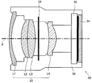
- FIG. 3 is a cross-sectional view schematically showing an embodiment of an imaging apparatus having a solid-state imaging device.
- the imaging device 50 includes, for example, a solid-state imaging device 51, a cover glass 52, a lens group 53, a diaphragm 54, and a housing 55 for fixing them.
- the lens group 53 is disposed on the imaging surface side of the solid-state imaging device 51, and includes, for example, a first lens L1, a second lens L2, a third lens L3, and a fourth lens L4.
- the stop 54 is disposed between the third lens L3 and the fourth lens L4.
- the cover glass 52 is disposed on the lens group 53 side of the solid-state image sensor 51 and protects the solid-state image sensor 51 from the external environment.
- the solid-state imaging device 51 is an electronic component that converts light that has passed through the lens group 53 into an electrical signal, and is, for example, a CCD or a CMOS.
- the solid-state image sensor 51, the cover glass 52, the lens group 53, and the stop 54 are disposed along the optical axis x.
- the imaging device 50 In the imaging device 50, light incident from the subject side passes through the first lens L 1, the second lens L 2, the third lens L 3, the diaphragm 54, the fourth lens L 4, and the cover glass 52, and the solid-state imaging device. 51 is incident.
- the solid-state image sensor 51 converts the incident light into an electric signal and outputs it as an image signal.
- the optical member 1 is used as, for example, the cover glass 52 and the lens group 53, that is, the first lens L1, the second lens L2, the third lens L3, or the fourth lens L4.
- the first dielectric multilayer film 3 and the second dielectric multilayer film 4 of the optical member 1 use the cover glass or lens group of a conventional imaging device as the transparent base material 2, and the surface of the transparent base material 2. Is provided.
- optical member 1 will be described more specifically with reference to examples.
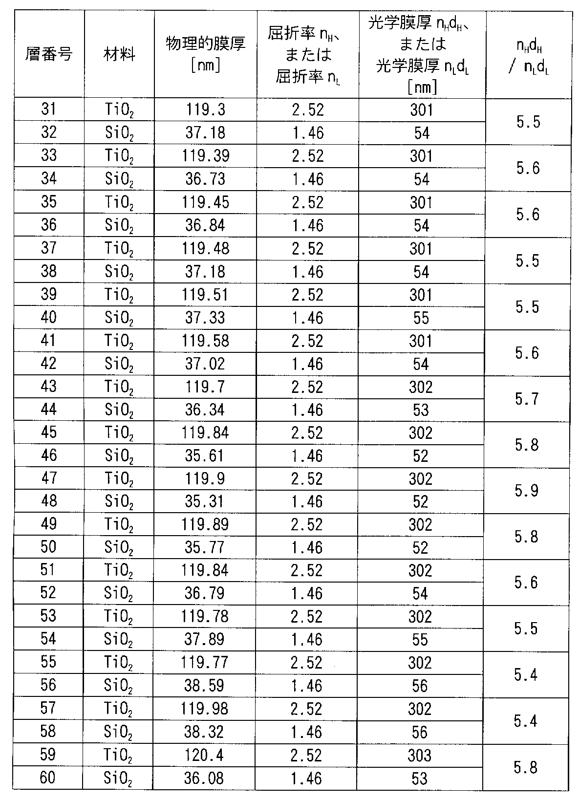
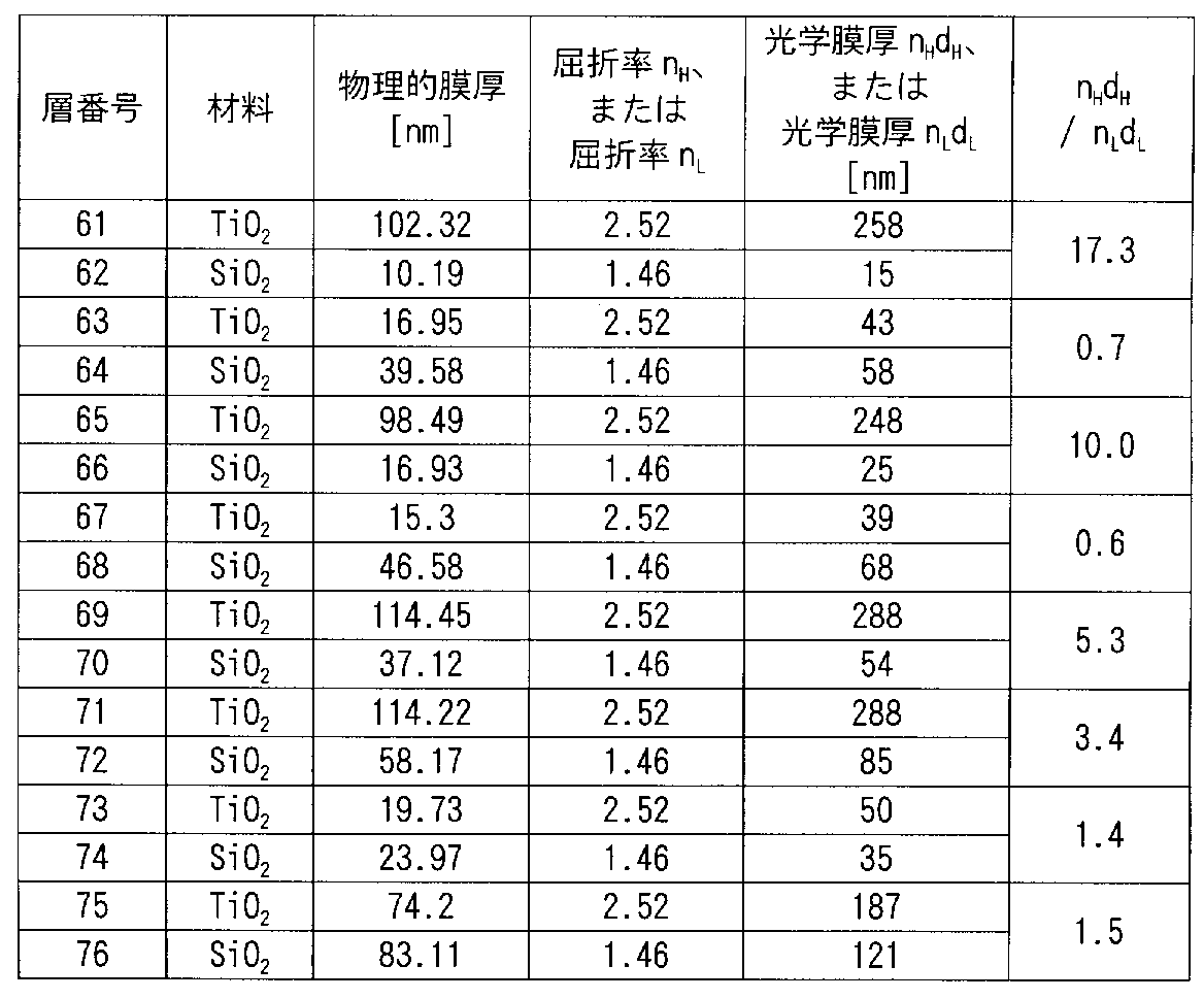
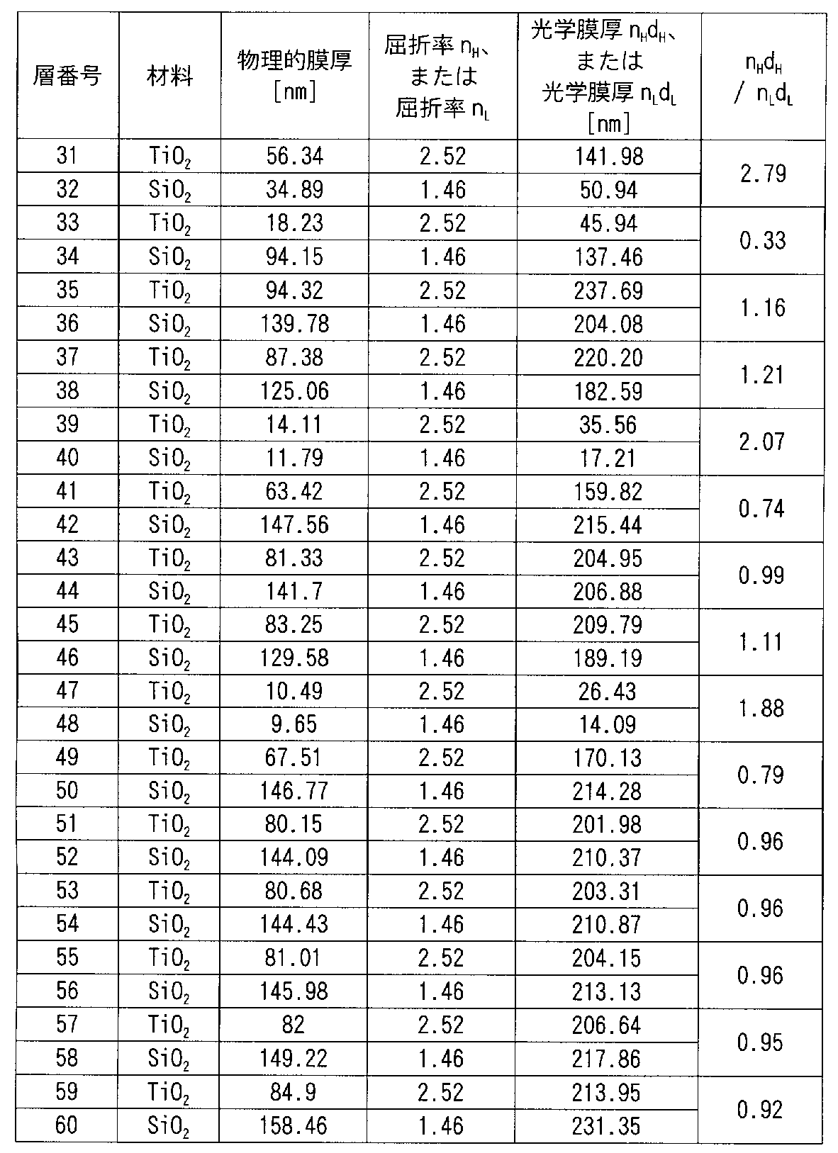
- Example 1 A TiO 2 film as a high refractive index layer 31 and an SiO 2 film as a low refractive index layer 32 are formed on one surface of a 1 mm thick soda glass plate as the transparent substrate 2 as shown in Tables 1 to 3.
- the first dielectric multilayer film 3 is formed by alternately laminating. Further, as shown in Tables 4 to 6, the TiO 2 film as the high refractive index layer 41 and the SiO 2 film as the low refractive index layer 42 are alternately stacked on the other surface of the transparent substrate 2.
- the dielectric multilayer film 4 is formed, and the optical member 1 is manufactured.
- the total number of layers including the high refractive index layer 31 and the low refractive index layer 32 is 76, that is, the total number of unit refractive index layers 33 is 38, n H d
- the number of unit refractive index layers 33 satisfying H 2 / n L d L ⁇ 3 is 28, and the number of unit refractive index layers 33 satisfying n H d H / n L d L ⁇ 5 is 25, 5 ⁇ n
- the number of unit refractive index layers 33 satisfying H d H / n L d L ⁇ 8 is 23, the average n H d H / n L d L is 4.8, the average optical film thickness n H d H is 232 nm, The average optical film thickness n L d L is 54 nm.
- the total number of layers of the high refractive index layer 41 and the low refractive index layer 42 is 90, that is, the total number of unit refractive index layers 43 is 45, and the average n H d H / N L d L is 1.2, the average optical film thickness n H d H is 143 nm, and the average optical film thickness n L d L is 145 nm.
- the transmittance in the range of 350 to 395 nm is less than 3%, and the average transmittance in the range of 430 to 630 nm is 95% or more.
- the minimum transmittance is 90% or more, the average transmittance in the range of 700 to 1000 nm is less than 0.1%, the maximum transmittance in the same range is less than 0.5%, and the average transmittance in the range of 1000 to 1100 nm is 0.00. Less than 5%, the maximum transmittance in the same range is less than 2%, and the transmittance is 50% within the range of 415 ⁇ 10 nm and the range of 650 ⁇ 6 nm.
- a TiO 2 film and a SiO 2 film are alternately laminated on one surface of a glass plate similar to the glass plate used in Example 1 to shield the infrared wavelength region.
- a multilayer film is formed.
- the TiO 2 film and the SiO 2 film are alternately laminated on the other surface of the glass plate as shown in Tables 4-6. Then, a dielectric multilayer film for shielding the ultraviolet wavelength region and the infrared wavelength region is formed to manufacture an optical member.
- ⁇ 0 is the central wavelength 760 nm of the reflection band.
- a TiO 2 film and a SiO 2 film are alternately laminated on one surface of a glass plate similar to the glass plate used in Example 1 to shield the infrared wavelength region.
- a multilayer film is formed.
- the TiO 2 film and the SiO 2 film are alternately laminated on the other surface of the glass plate as shown in Tables 4-6. Then, a dielectric multilayer film for shielding the ultraviolet wavelength region and the infrared wavelength region is formed to manufacture an optical member.
- ⁇ 0 is the central wavelength of the reflection band, 680 nm.
- FIG. 4 shows the spectral transmittance when the incident angle ⁇ is 0 ° in the wavelength range of 600 to 700 nm and the spectral transmittance when the incident angle ⁇ is 30 ° for the optical members of Example 1 and Comparative Examples 1 and 2. Indicates the rate.
- FIG. 4 shows the spectral transmittance when the incident angle ⁇ is 0 ° in the wavelength range of 600 to 700 nm and the spectral transmittance when the incident angle ⁇ is 30 ° for the optical members of Example 1 and Comparative Examples 1 and 2. Indicates the rate.
- the refractive index of the high refractive index layer takes wavelength dependency into consideration.
- the number of layers is 10 or more, specifically at n H d H / n L d L ⁇ 3 layer number which satisfies the 28, n H d H / n L d L ⁇ 5 number of layers is 25 to satisfy the
- the difference between the 50% transmission wavelength when the incident angle ⁇ is 0 ° and the 50% transmission wavelength when the incident angle ⁇ is 30 ° in the cutoff band near 650 nm is 16 nm.
- the incident angle dependency can be effectively reduced.
- the optical member 1 of Example 1 can effectively reduce the incident angle dependency, and can effectively improve the transmittance ripple, that is, the flatness of the spectral transmittance.
- Example 2 As shown in Table 13, a TiO 2 film as the high refractive index layer 31 and an SiO 2 film as the low refractive index layer 32 are alternately formed on one surface of a 1 mm thick soda glass plate as the transparent substrate 2. By stacking, the first dielectric multilayer film 3 is formed, and the optical member 1 is manufactured.
- the total number of layers including the high refractive index layer 31 and the low refractive index layer 32 is 30, that is, the total number of unit refractive index layers 33 is 15, n H d
- the number of unit refractive index layers 33 satisfying H 1 / n L d L ⁇ 3 is 13, and the number of unit refractive index layers 33 satisfying n H d H / n L d L ⁇ 5 is 12, 5 ⁇ n
- the number of unit refractive index layers 33 satisfying H d H / n L d L ⁇ 8 is 12, the average n H d H / n L d L is 5.5, the average optical film thickness n H d H is 283 nm, The average optical film thickness n L d L is 48 nm.
- the transmittance in the range of 360 to 395 nm is less than 3%, and the average transmittance in the range of 430 to 630 nm is 95% or more.
- the minimum transmittance is 90% or more, and the transmittance is 50% within the range of 415 ⁇ 10 nm and 650 ⁇ 6 nm.
- the spectral transmittance when the incident angle ⁇ was 0 ° and the spectral transmittance when the incident angle ⁇ was 30 ° were determined by optical simulation.
- FIG. 6 shows the spectral transmittance when the incident angle ⁇ is 0 ° in the wavelength range of 350 to 1100 nm, and the spectral transmittance when the incident angle ⁇ is 30 °.
- the refractive index of the high refractive index layer takes wavelength dependency into consideration.
- the number of unit refractive index layers 33 satisfying n H d H / n L d L ⁇ 3 in the first dielectric multilayer film 3 is 13, and n H d H / n L
- the 50% transmission wavelength and the incident angle ⁇ are 30 ° when the incident angle ⁇ is 0 ° in the cutoff band near 650 nm.
- the difference from the 50% transmission wavelength can be 16 nm, and the incident angle dependency can be effectively reduced.
- Example 3 On one surface of a near-infrared cut filter glass (NF-50 glass manufactured by Asahi Glass Co., Ltd., having a glass thickness of 0.3 mm) as the transparent substrate 2, TiO as the high refractive index layer 31 as shown in Tables 14 to 16 2 film and the SiO 2 film as a low-refractive index layer 32 to form the first dielectric multilayer film 3 stacked alternately. Further, as shown in Table 17, a TiO 2 film as the high refractive index layer 41 and an SiO 2 film as the low refractive index layer 42 are alternately laminated on the other surface of the transparent substrate 2 to form the second The dielectric multilayer film 4 is formed, and the optical member 1 is manufactured.
- NF-50 glass manufactured by Asahi Glass Co., Ltd. having a glass thickness of 0.3 mm
- the total number of layers including the high refractive index layer 31 and the low refractive index layer 32 is 76, that is, the total number of unit refractive index layers 33 is 38, n H d
- the number of unit refractive index layers 33 satisfying H 2 / n L d L ⁇ 3 is 28, and the number of unit refractive index layers 33 satisfying n H d H / n L d L ⁇ 5 is 20, 5 ⁇ n
- the number of unit refractive index layers 33 satisfying H d H / n L d L ⁇ 8 is 17, the average n H d H / n L d L is 5.1, the average optical film thickness n H d H is 247 nm, The average optical film thickness n L d L is 58 nm.
- the total number of layers including the high refractive index layer 41 and the low refractive index layer 42 is 12, that is, the total number of unit refractive index layers 43 is 6, and the average n H d H / N L d L is 1.1, the average optical film thickness n H d H is 211 nm, and the average optical film thickness n L d L is 190 nm.
- the transmittance in the range of 350 to 395 nm is less than 3%, and the average transmittance in the range of 430 to 545 nm is 95% or more.
- the minimum transmittance is 90% or more, the average transmittance in the range of 700 to 1000 nm is less than 0.1%, the maximum transmittance in the same range is less than 0.5%, and the average transmittance in the range of 1000 to 1100 nm is 0.00. Less than 5%, the maximum transmittance in the same range is less than 2%, and the transmittance is 50% within the range of 415 ⁇ 10 nm and the range of 640 ⁇ 6 nm.
- the spectral transmittance when the incident angle ⁇ was 0 ° and the spectral transmittance when the incident angle ⁇ was 30 ° were determined by optical simulation.
- FIG. 7 shows the spectral transmittance when the incident angle ⁇ is 0 ° in the wavelength range of 400 to 1100 nm, and the spectral transmittance when the incident angle ⁇ is 30 °.
- the refractive index of each refractive index layer does not consider wavelength dependence.
- the optical member 1 of Example 3 in which the transparent substrate 2 was changed also has an incident angle ⁇ with respect to a 50% transmission wavelength of 638 nm when the incident angle ⁇ in the cutoff band is 0 °.
- the 50% transmission wavelength when the incident angle ⁇ is 30 ° can be 635 nm, and the 20% transmission wavelength 686 nm when the incident angle ⁇ is 0 ° in the same cutoff band.
- the wavelength can be 671 nm, and the incident angle dependency can be effectively reduced.
- Comparative Example 3 As shown in Tables 18 and 19, mainly a TiO 2 film and an Al 2 O 3 film are alternately laminated on one surface of a glass plate similar to the glass plate used in Example 1 for shielding the infrared wavelength region.
- the dielectric multilayer film is formed.
- the films described in the layer numbers 1, 2, and 35 are adjustment layers, and the film having the layer numbers 3 to 34 is a dielectric multilayer film for shielding the infrared wavelength region.
- the TiO 2 film and the SiO 2 film are alternately laminated on the other surface of the glass plate as shown in Tables 4-6.
- a dielectric multilayer film for shielding the ultraviolet wavelength region and the infrared wavelength region is formed to manufacture an optical member.
- the infrared multi-layer shielding dielectric multilayer films shown in Tables 18 and 19 have a high refractive index layer and a middle refractive index layer (made of constituent materials having a refractive index of more than 1.6 and less than 2). This is a repeated configuration.
- Comparative Example 4 As shown in Tables 18 and 19, TiO 2 films and Al 2 O 3 films similar to those of Comparative Example 3 are alternately laminated on one surface of a glass plate similar to the glass plate used in Example 1. A dielectric multilayer film for shielding the outer wavelength region is formed. The difference from Comparative Example 3 is that no dielectric multilayer film is formed on the other surface of the glass plate.
- the spectral transmittance when the incident angle ⁇ was 0 ° and the spectral transmittance when the incident angle ⁇ was 30 ° were determined by optical simulation.
- 8 and 9 show the spectral transmittance when the incident angle ⁇ is 0 ° in the wavelength range of 300 to 1300 nm, and the spectral transmittance when the incident angle ⁇ is 30 °.
- the refractive index of each refractive index layer takes wavelength dependency into consideration.
- the 50% transmission wavelength and the incident angle ⁇ are 30 ° when the incident angle ⁇ is 0 ° in the cutoff band near 650 nm.
- the difference from the 50% transmission wavelength is as large as 22 nm, and the incident angle dependency cannot be reduced.
- Example 4 On one surface of a 1 mm thick soda glass plate as the transparent substrate 2, a TiO 2 film as a high refractive index layer 31 and an SiO 2 film as a low refractive index layer 32 as shown in Tables 20 and 21.
- the first dielectric multilayer film 3 is formed by alternately stacking, and the optical member 1 is manufactured.
- the total number of layers including the high refractive index layer 31 and the low refractive index layer 32 is 42, that is, the total number of unit refractive index layers 33 is 21, n H d
- the number of unit refractive index layers 33 satisfying H 1 / n L d L ⁇ 3 is 13, and the number of unit refractive index layers 33 satisfying n H d H / n L d L ⁇ 5 is 13, 5 ⁇ n
- the number of unit refractive index layers 33 satisfying H d H / n L d L ⁇ 8 is 8, the average n H d H / n L d L is 5.2, and the average optical film thickness n H d H is 99.
- the average optical film thickness n L d L is 45.8 nm and 45.8 nm.
- the layer numbers 1 to 10 and 29 to 42 of the first dielectric multilayer film 3 also function as an adjusting unit.
- the adjustment unit is T H / TL is 0.87.
- the transmittance in the range of 360 to 395 nm is less than 3%, and the average transmittance in the range of 430 to 630 nm is 95% or more.
- the minimum transmittance is 90% or more in the range of 415 ⁇ 10 nm, specifically in the range of 415 to 416 nm, and in the range of 650 ⁇ 15 nm, specifically in the range of 660 to 661 nm. % Has a point.
- the spectral transmittance when the incident angle ⁇ was 0 ° and the spectral transmittance when the incident angle ⁇ was 30 ° were determined by optical simulation.
- FIG. 10 shows the spectral transmittance when the incident angle ⁇ is 0 ° in the wavelength range of 350 to 1100 nm, and the spectral transmittance when the incident angle ⁇ is 30 °.
- the refractive index of each refractive index layer takes wavelength dependency into consideration.
- the number of unit refractive index layers 33 satisfying n H d H / n L d L ⁇ 3 in the first dielectric multilayer film 3 is 13, and n H d H / n L
- the 50% transmission wavelength and the incident angle ⁇ are 30 ° when the incident angle ⁇ is 0 ° in the cutoff band near 650 nm.
- the difference from the 50% transmission wavelength can be 8 nm, and the incident angle dependency can be effectively reduced.
- the waveform shift between the incident angle ⁇ of 0 ° and the incident angle ⁇ of 30 ° in the cutoff band near 650 nm is parallel. In other words, it is considered that the waveform is deformed.
- the wavelength shift amount when the incident angle ⁇ in this range changes from 0 ° to 30 ° is 10 nm. It can be seen that the amount of wavelength shift is very small.
- the wavelength region where the near infrared transmittance is less than 50% has a larger wavelength shift amount than the wavelength shift amount in the wavelength region where the transmittance is 50 to 90%. Therefore, by using a part of the first dielectric multilayer film 3 as an adjustment unit, the wavelength shift amount depending on the incident angle on the near infrared side is made non-uniform, and the incident angle dependency of the wavelength range in the red region is reduced. Can be small.
- SYMBOLS 1 Optical member, 2 ... Transparent base material, 3 ... 1st dielectric multilayer film, 4 ... 2nd dielectric multilayer film, 31 ... High refractive index layer, 32 ... Low refractive index layer, 41 ... High refractive index Layer, 42 ... low refractive index layer, 50 ... imaging device, 51 ... solid-state imaging device, 52 ... cover glass, 53 ... lens group, 54 ... stop, 55 ... casing.
Landscapes
- Physics & Mathematics (AREA)
- General Physics & Mathematics (AREA)
- Optics & Photonics (AREA)
- Optical Filters (AREA)
Abstract
光学部材1は、透明基材2と、該透明基材2に形成され、屈折率が2以上の高屈折率層31と屈折率が1.6以下の低屈折率層32とからなる単位屈折率層33が複数積層された誘電体多層膜3とを有する。光学部材1は、特に、誘電体多層膜3における単位屈折率層3の全層数が15以上、かつ単位屈折率層3における高屈折率層31の光学膜厚をnHdH、低屈折率層32の光学膜厚をnLdLとしたとき、誘電体多層膜3におけるnHdH/nLdL≧3を満足する単位屈折率層3の層数が10以上である。
Description
本発明は、誘電体多層膜を有する光学部材に関する。
デジタルスチルカメラ等の撮像装置では、CCD(Charge Coupled Device)やCMOSイメージセンサ(Complementary Metal Oxide Semiconductor Image Sensor)等の固体撮像素子を用いて被写体を撮像している。これらの固体撮像素子は可視域から1100nm付近の近赤外波長域に亘る分光感度を有しており、単体では良好な色再現性を得ることができないことから、赤外波長域の光を遮蔽するフィルタを用いて人の通常の視感度に補正している。すなわち、撮像レンズから固体撮像素子までの光路中に赤外波長域の光を遮蔽するフィルタを設けている。このような用途に用いられるフィルタには、可視波長域の光の透過率が高いことが要求され、例えば、特許文献1にあるように高屈折率層と低屈折率層とを交互に複数積層した誘電体多層膜が用いられる。
しかしながら、誘電体多層膜を有するフィルタは、光の入射角依存性を有しており、撮像装置に適用した場合、撮像レンズを通してフィルタに入射する光の入射角によってカットオフ波長が移動するため、撮影した画像の中心部と周辺部とで色目が変化することがある。以下、光の入射角依存性は単に入射角依存性という。
入射角依存性を低減する方法として、例えば第1の誘電体多層膜と第2の誘電体多層膜とを設け、第1の誘電体多層膜の反射帯域の幅を第2の誘電体多層膜の反射帯域の幅より狭くするとともに、第2の誘電体多層膜の短波長側エッジの位置を第1の誘電体多層膜の反射帯域の短波長側エッジと長波長側エッジとの間とし、特に第1の誘電体多層膜全体の平均屈折率を第2の誘電体多層膜全体の平均屈折率よりも高くする方法が知られている。このような方法では、平均屈折率が高い第1の誘電体多層膜によって入射角依存性を低減し、第2の誘電体多層膜と合わせて広い反射帯域を確保する。特許文献2はこのような例である。
また、ダイクロイックミラーとして、高屈折率層と中屈折率層とからなる第1の選択透過多層膜と、屈折率比の大きい高屈折率層と低屈折率層とからなる第2の選択透過多層膜とを組み合わせる方法が知られている。このような方法では、高屈折率層と中屈折率層とからなる第1の選択透過多層膜によって入射角依存性を低減する。特許文献3はこのような例である。
特許文献2にも記載されるように、単に誘電体多層膜の平均屈折率を高くした場合、例えば、TiO2からなる高屈折率層と、SiO2よりも屈折率の高いTa2O5等からなる中屈折率層とを交互に繰り返し積層した場合、反射帯域の幅が狭く、かつ反射率が低くなりやすい。このため、特許文献2、3に記載されるように、TiO2からなる高屈折率層とSiO2よりも屈折率の高いTa2O5等からなる中屈折率層とからなる平均屈折率が高い誘電体多層膜と、高屈折率層と低屈折率層とからなる平均屈折率が低い誘電体多層膜とを併用する方法も知られているが、構成材料の異なる屈折率層を追加で形成する必要があり、必ずしも生産性に優れない。
本発明は、上記課題を解決するためになされたものであって、屈折率が2以上の高屈折率層と屈折率が1.6以下の低屈折率層とを交互に積層した誘電体多層膜を有する光学部材において、入射角依存性の低減を目的とする。
本発明の光学部材は、透明基材と、前記透明基材に形成され、屈折率が2以上の高屈折率層と屈折率が1.6以下の低屈折率層とからなる単位屈折率層が複数積層された誘電体多層膜とを有する。本発明の光学部材は、特に、前記誘電体多層膜における前記単位屈折率層の全層数が15以上、かつ前記単位屈折率層における前記高屈折率層の光学膜厚をnHdH、前記低屈折率層の光学膜厚をnLdLとしたとき、前記誘電体多層膜におけるnHdH/nLdL≧3を満足する単位屈折率層の層数が10以上であることを特徴とする。
本発明の光学部材によれば、屈折率が2以上の高屈折率層と屈折率が1.6以下の低屈折率層とからなる単位屈折率層が複数積層された誘電体多層膜を有するものであって、誘電体多層膜における単位屈折率層の全層数を15以上、かつ誘電体多層膜におけるnHdH/nLdL≧3を満足する単位屈折率層の層数を10以上とすることで、入射角依存性を効果的に低減できる。
以下、本発明の光学部材について説明する。本発明の光学部材1は、透明基材2と、この透明基材2に形成された誘電体多層膜3とを有する。誘電体多層膜3は、屈折率が2以上の高屈折率層31と屈折率が1.6以下の低屈折率層32とからなる単位屈折率層33が複数積層されて構成される。なお、屈折率は、波長550nmの光に対する屈折率を意味する。
本発明の光学部材1は、誘電体多層膜3における単位屈折率層33の全層数が15以上であることを特徴とする。また、単位屈折率層33における高屈折率層31の光学膜厚をnHdH、低屈折率層32の光学膜厚をnLdLとしたとき、誘電体多層膜3におけるnHdH/nLdL≧3を満足する単位屈折率層33の層数が10以上であることを特徴とする。
なお、誘電体多層膜3は、必ずしも単位屈折率層33のみから構成される必要はなく、厚さ方向、すなわち単位屈折率層33の積層方向の一方または双方に、単位屈折率層33を構成しない単独で存在する高屈折率層31または低屈折率層32を有してもよい。また、nHdH/nLdL≧3を満足する10以上の単位屈折率層33については、互いにnHdH/nLdLが同一であってもよいし、異なってもよい。以下では、このような誘電体多層膜3を第1の誘電体多層膜3と記すことがある。
本発明の光学部材1によれば、特に誘電体多層膜3におけるnHdH/nLdL≧3を満足する単位屈折率層33の層数を10以上とすることで、屈折率が2以上の高屈折率層31と屈折率が1.6以下の低屈折率層32とからなる単位屈折率層33を複数積層するものにおいて、入射角依存性を効果的に低減できる。具体的には、透過帯域と反射帯域との間のカットオフ帯域、通常は650nm付近のカットオフ帯域における入射角0°における50%透過波長と入射角30°における50%透過波長との差を例えば16nm以下に低減できる。以下、上記差を赤外線側半値波長シフト量または単に波長シフト量と記す場合がある。本発明の光学部材1においては、入射角依存性をより効果的に低減する観点から、nHdH/nLdL≧5を満足する単位屈折率層33の層数が10以上であることが好ましい。
誘電体多層膜3における単位屈折率層33の全層数、および誘電体多層膜3におけるnHdH/nLdL≧3、好ましくはnHdH/nLdL≧5を満足する単位屈折率層33の層数は、入射角依存性を低減するとともに、透過率リップル、すなわち分光透過率の平坦性を改善する観点から、より多いことが好ましい。例えば、誘電体多層膜3における単位屈折率層33の全層数は、30以上が好ましく、35以上がより好ましい。また、誘電体多層膜3におけるnHdH/nLdL≧3、好ましくはnHdH/nLdL≧5を満足する単位屈折率層33の層数は、15以上が好ましく、18以上がより好ましい。誘電体多層膜3における単位屈折率層33の全層数、および誘電体多層膜3におけるnHdH/nLdL≧3、好ましくはnHdH/nLdL≧5を満足する単位屈折率層33の層数を上記範囲とすることで、特に650nm付近のカットオフ帯域における入射角0°における50%透過波長と入射角30°における50%透過波長との差を16nm以下に低減するとともに、透過率リップルを低減しやすい。
誘電体多層膜3における単位屈折率層33の全層数、および誘電体多層膜3におけるnHdH/nLdL≧3、好ましくはnHdH/nLdL≧5を満足する単位屈折率層33の層数は、赤外域遮蔽の観点からは多いことが好ましいが、生産性の観点からは抑制することが好ましい。従って、誘電体多層膜3における単位屈折率層33の全層数は45以下が好ましく、40以下がより好ましい。また、誘電体多層膜3におけるnHdH/nLdL≧3、好ましくはnHdH/nLdL≧5を満足する単位屈折率層33の層数は、35以下が好ましく、30以下がより好ましい。
また、誘電体多層膜3におけるnHdH/nLdL≧3、好ましくはnHdH/nLdL≧5を満足する単位屈折率層33は、5≦nHdH/nLdL≦8を満足することが好ましい。誘電体多層膜3における5≦nHdH/nLdL≦8を満足する単位屈折率層33の層数は、10以上が好ましく、15以上がより好ましい。このようなものとすることで、650nm付近のカットオフ帯域における入射角0°における50%透過波長と入射角30°における50%透過波長との差を16nm以下とするとともに、透過率リップルを低減しやすい。
誘電体多層膜3における単位屈折率層33の全体、すなわちnHdH/nLdL≧3を満足する単位屈折率層33とnHdH/nLdL<3である単位屈折率層33とを合わせた全体におけるnHdH/nLdLの平均値である平均nHdH/nLdLは4.5~6が好ましい。特に、誘電体多層膜3における単位屈折率層33の全層数が多い場合、例えば誘電体多層膜3における単位屈折率層33の全層数が30以上の場合、平均nHdH/nLdLは4.5~5.3が好ましい。
誘電体多層膜3における個々の単位屈折率層33のnHdH/nLdLは、上記条件を満たせば必ずしも制限されないが、0.1~25が好ましく、0.2~20が好ましい。なお、上記したように、誘電体多層膜3における10以上の単位屈折率層33については、nHdH/nLdL≧3、好ましくはnHdH/nLdL≧5を満足し、より好ましくは5≦nHdH/nLdL≦8を満足する。
誘電体多層膜3における高屈折率層31の光学膜厚nHdHの平均値である平均光学膜厚nHdHは、200~310nmが好ましく、210~300nmがより好ましい。誘電体多層膜3における低屈折率層32の光学膜厚nLdLの平均値である平均光学膜厚nLdLは、40~70nmが好ましく、40~65nmがより好ましい。特に、誘電体多層膜3における単位屈折率層33の全層数が多い場合、例えば誘電体多層膜3における単位屈折率層33の全層数が30以上の場合、高屈折率層31の光学膜厚nHdHの平均値である平均光学膜厚nHdHは、210~270nmが好ましく、220~260nmがより好ましい。また、誘電体多層膜3における低屈折率層32の光学膜厚nLdLの平均値である平均光学膜厚nLdLは、45~70nmが好ましく、45~65nmがより好ましい。
誘電体多層膜3における個々の高屈折率層31の光学膜厚nHdHは、上記条件を満たすものであれば必ずしも制限されないが、10~350nmが好ましい。誘電体多層膜3における個々の低屈折率層32の光学膜厚nLdLについても、上記条件を満たすものであれば必ずしも制限されないが、10~140nmが好ましい。
高屈折率層31の構成材料は、屈折率が2以上であれば必ずしも制限されないが、例えば、TiO2、Nb2O5、Ta2O5、これらの複合酸化物等が挙げられる。また、低屈折率層32の構成材料についても、屈折率が1.6以下であれば必ずしも制限されないが、例えば、SiO2、MgF2、これらの複合酸化物等が挙げられる。高屈折率層31、低屈折率層32には、上記屈折率を満たす範囲内で、屈折率を調整するための添加剤を含有させることができる。添加剤としては、例えば、SiO2、Al2O3、CeO2、FeO2、HfO2、In2O3、MgF2、Nb2O3、SnO2、Ta2O3、TiO2、Y2O3、ZnO、ZrO2、NiO、ITO(Indium Tin Oxide)、ATO(Antimony doped Tin Oxide)、MgO等が挙げられる。
前記高屈折率層31および前記低屈折率層32は、それぞれ単一の構成材料からなることが好ましい。このようにすることで、誘電体多層膜3を形成する際の膜厚調整機構が2つの構成材料にのみ対応すればよく、また膜材料も2種類のみとなるため、成膜工程における生産性を向上させることが可能となる。
高屈折率層31、低屈折率層32は、例えば、スパッタリング法、真空蒸着法、イオンビーム法、イオンプレーティング法、CVD法により形成する。これらの形成方法によれば、各屈折率層の厚さを高精度に制御しながら、各屈折率層を比較的容易に形成できる。また、スパッタリング法やイオンプレーティング法は、いわゆるプラズマ雰囲気処理であることから、透明基材2に対する誘電体多層膜3の密着性を向上できる。
透明基材2は、無色および有色のいずれであってもよく、可視波長域の光を透過するものであれば、その形状は特に限定されるものではなく、例えば、板状、フィルム状、ブロック状、レンズ状等が挙げられる。
透明基材2の構成材料としては、ガラス、水晶、ニオブ酸リチウム、サファイヤ等の結晶、ポリエチレンテレフタレート(PET)、ポリブチレンテレフタレート(PBT)等のポリエステル樹脂、ポリエチレン、ポリプロピレン、エチレン酢酸ビニル共重合体等のポリオレフィン樹脂、ノルボルネン樹脂、ポリアクリレート、ポリメチルメタクリレート等のアクリル樹脂、ウレタン樹脂、塩化ビニル樹脂、フッ素樹脂、ポリカーボネート樹脂、ポリビニルブチラール樹脂、ポリビニルアルコール樹脂等が挙げられる。これらの材料は、紫外波長域および赤外波長域の少なくとも一方に対して吸収特性を有するものであってもよい。
ガラスは、可視波長域で透明な材料から、使用する装置、配置する場所等を考慮して、アルカリ成分の有無や線膨張係数の大きさ等の特性を適宜選択して使用できる。硼珪酸ガラスは、加工が容易で、光学面における傷や異物等の発生を抑制できるために好ましく、アルカリ成分を含まないガラスは、接着性、耐候性等が良好なために好ましい。また、ガラスとしては、フツリン酸塩系ガラスやリン酸塩系ガラスにCuO等が添加された赤外波長域に吸収を有する吸収型のガラスであってもよい。
透明基板2は、赤外波長域に吸収を有することが好ましい。本発明の光学部材1を撮像装置用の近赤外線カットフィルタとして用いる場合、透明基板2が赤外波長域に吸収を有することで、人の視感度特性に近い色補正が可能となる。誘電体多層膜3は、透明基板2の吸収が十分でない部分を補完する目的で用いられる。誘電体多層膜3を用いることで、入射角依存性の低い分光特性が得られるため、透明基板2の分光特性に悪影響を及ぼすことがない。そのため、撮像装置用の近赤外線カットフィルタとして良好な特性を有する光学部材1を得ることが可能となる。
水晶、ニオブ酸リチウム、サファイヤ等の結晶は、デジタルスチルカメラ、デジタルビデオカメラ、監視カメラ、車載用カメラ、ウェブカメラ等の撮像装置において、モアレや偽色を低減するためのローパスフィルタや波長板として使用されており、光学部材1にローパスフィルタや波長板の機能を付与し、例えば撮像装置を小型化および薄型化できる。
撮像装置における固体撮像素子または固体撮像素子パッケージには、一般に固体撮像素子を保護するためのカバーが気密封着される。このカバーを透明基材2として利用することで、該カバーに赤外線遮蔽機能を付与するとともに、入射角依存性を低減できる。カバーの材料としては、結晶、ガラス、樹脂が挙げられるが、耐熱性の観点から結晶またはガラスが好ましい。樹脂を選択する場合、耐熱性に優れる材料、例えば、アクリル樹脂、シリコーン樹脂、フッ素樹脂、シルセスキオキサン等を含有する有機無機ハイブリッド材料等が好ましい。
誘電体多層膜3は、以下の調整部を含んでもよい。誘電体多層膜3は、入射角依存性が低い分光特性が得られるものであるが、その一部の構成を調整部とすることで、特に赤外線側半値波長シフト量をより小さくすることができる。例えば、調整部を含む誘電体多層膜3によれば、光学部材1の赤外線側半値波長シフト量を10nm以下にできる。
調整部は、単独での分光特性における入射角依存性が高く、斜入射時に波形変形を生じることが特徴である。具体的には、調整部による近赤外側半値波長付近の波形が斜入射とともに大きく変化することで、誘電体多層膜3の全体による近赤外側半値波長付近の波長シフト量が結果的に小さくなる。調整部以外の誘電体多層膜3による近赤外側半値波長付近の波形シフトは斜入射とともに相似形で平行にシフトするが、調整部による波形シフトは波形変形を伴いながら、つまり相似形でない形でシフトする。これらを組み合わせることで、基本的には波長シフト量が小さく、かつ波形変形を利用することで近赤外側半値波長の波長シフト量を極めて小さくすることが可能である。なお、このような調整部の斜入射時の波形変形は、入射角度の変化に伴う光学的膜厚変化から生じている。
調整部は、誘電体多層膜3における屈折率が2以上の高屈折率層31と屈折率が1.6以下の低屈折率層32との少なくとも一部から構成されるものであって、高屈折率層31と低屈折率層32との合計層数が10層以上、かつ、高屈折率層31の平均光学膜厚をTH、低屈折率層32の平均光学膜厚をTLとしたとき、TH/TLが1.5以下のものが好ましい。このようなものとすることで、上記したような分光特性とすることができる。
なお、高屈折率層31の平均光学膜厚THは、調整部を構成する高屈折率層31の光学膜厚の合計を、調整部を構成する高屈折率層31の層数で除したものである。同様に、低屈折率層32の平均光学膜厚TLは、調整部を構成する低屈折率層32の光学膜厚の合計を、調整部を構成する低屈折率層32の層数で除したものである。ここで、調整部は、必ずしも10層以上が連続して形成される必要はなく、2以上の部分に分割して形成されてもよい。分割して形成される場合、少なくとも1つの部分の層数は10層以上であることが好ましい。また、分割して形成される場合、それぞれの部分については必ずしもTH/TLが1.5以下となっている必要はなく、全ての部分を合わせた全体についてTH/TLが1.5以下となっていればよい。
調整部の合計層数は、基本的に多くなるほど所定の分光特性を得やすくなるために好ましいが、生産性等の観点から100層以下が好ましく、50層以下が好ましい。また、TH/TLについても、1.5以下であれば必ずしも制限されないが、所定の分光特性を得やすいことから1.0以下が好ましく、0.9以下がより好ましい。TH/TLは、通常、0.1以上が好ましく、0.3以上がより好ましい。
誘電体多層膜3で調整部を用いた場合と用いない場合との赤外側カットオフ領域の透過率1~95%での平均波長シフト量はほとんど変わらない。これは、誘電体多層膜3における斜入射での波形シフトへの影響は、調整部以外の誘電体多層膜3の構成による分光特性が支配的であるためと考えられる。しかしながら、光学部材を撮像装置用の近赤外線カットフィルタとして用いる場合には、調整部を用いることで透過率が50%を超える領域の波形シフトを小さくでき、これにより赤色域の波長範囲の入射角依存性を小さくすることができるため、撮像装置における画像向上に寄与することができる。
上記観点から、調整部を有する光学部材1は、以下の分光特性を有することが好ましい。すなわち、入射角θが0°から30°に変化した際の近赤外側の透過率が50%~90%となる波長領域のシフト量が10nm以下になることが好ましい。これにより、赤色域の波長範囲(630nm付近)の波長シフトが抑制され、撮像装置における画像向上に寄与することができる。また、この効果を得るために、近赤外側半値波長は、入射角θが0°のとき600~700nmの範囲にあることが好ましく、620~680nmの範囲にあることがより好ましい。
光学部材1には、上記した第1の誘電体多層膜3に加えて、図2に示すように、透明基材2の第1の誘電体多層膜3が設けられる主面とは反対側の主面に、紫外波長域および赤外波長域の長波長側の領域を遮蔽する第2の誘電体多層膜4を設けることができる。
第2の誘電体多層膜4としては、屈折率が2以上の高屈折率層41と屈折率が1.6以下の低屈折率層42とからなる単位屈折率層43を複数積層したものが挙げられる。第2の誘電体多層膜4における単位屈折率層43の全層数は、紫外線波長域および赤外波長域の光を効果的に遮蔽する観点から、3以上が好ましく、4以上がより好ましい。また、第2の誘電体多層膜4における単位屈折率層43の全層数は、生産性等との観点から、55以下が好ましく、50以下がより好ましい。
第2の誘電体多層膜4における単位屈折率層43の全体のnHdH/nLdLの平均値である平均nHdH/nLdLは、0.8~1.5が好ましく、0.9~1.4がより好ましい。また、第2の誘電体多層膜4における個々の単位屈折率層43のnHdH/nLdL値は、上記条件を満たせば必ずしも制限されないが、0.1~10が好ましく、0.1~8が好ましい。
第2の誘電体多層膜4における高屈折率層41の光学膜厚nHdHの平均値である平均光学膜厚nHdHは、100~250nmが好ましく、120~230nmがより好ましい。また、第2の誘電体多層膜4における低屈折率層42の光学膜厚nLdLの平均値である平均光学膜厚nLdLは、100~230nmが好ましく、120~210nmがより好ましい。
第2の誘電体多層膜4における個々の高屈折率層41の光学膜厚nHdHは、上記条件を満たせば必ずしも制限されないが、10~310nmが好ましく、15~300nmがより好ましい。第2の誘電体多層膜4における個々の低屈折率層42の光学膜厚nLdLについても、上記条件を満たせば必ずしも制限されないが、5~310nmが好ましく、10~300nmがより好ましい。
高屈折率層41の構成材料は、屈折率が2以上であれば必ずしも制限されないが、例えば、TiO2、Nb2O5、Ta2O5、これらの複合酸化物等が挙げられる。また、低屈折率層42の構成材料についても、屈折率が1.6以下であれば必ずしも制限されないが、例えば、SiO2、MgF2、これらの複合酸化物等が挙げられる。高屈折率層41、低屈折率層42には、上記屈折率を満たす範囲内で、屈折率を調整するための添加剤を含有させることができる。添加剤としては、例えば、SiO2、Al2O3、CeO2、FeO2、HfO2、In2O3、MgF2、Nb2O3、SnO2、Ta2O3、TiO2、Y2O3、ZnO、ZrO2、NiO、ITO(Indium Tin Oxide)、ATO(Antimony doped Tin Oxide)、MgO等が挙げられる。
高屈折率層41、低屈折率層42は、例えば、スパッタリング法、真空蒸着法、イオンビーム法、イオンプレーティング法、CVD法により形成する。これらの形成方法によれば、各屈折率層の厚さを高精度に制御しながら、各屈折率層を比較的容易に形成できる。また、スパッタリング法やイオンプレーティング法はいわゆるプラズマ雰囲気処理であることから、透明基材2に対する第2の誘電体多層膜4の密着性を向上できる。
光学部材1は、透過帯域と反射帯域との間のカットオフ帯域、通常は650nm付近のカットオフ帯域において、入射角0°における50%透過波長と入射角30°における50%透過波長との差が20nm以下であることが好ましく、18nm以下であることがより好ましい。光学部材1においては、第1の誘電体多層膜3におけるnHdH/nLdL≧3、好ましくはnHdH/nLdL≧5を満足する単位屈折率層33の層数を10以上、より好ましくは15以上、さらに好ましくは18以上とすることで、例えば入射角0°における50%透過波長と入射角30°における50%透過波長との差を16nm以下に低減することもできる。
光学部材1は、例えば、デジタルスチルカメラ、デジタルビデオカメラ、監視カメラ、車載用カメラ、ウェブカメラ等の撮像装置や自動露出計等の近赤外線カットフィルタ、すなわち視感度補正フィルタとして用いられる。デジタルスチルカメラ、デジタルビデオカメラ、監視カメラ、車載用カメラ、ウェブカメラ等の撮像装置においては、光学部材1は、例えば撮像レンズと固体撮像素子との間に配置される。自動露出計においては、例えば受光素子の前面に配置される。
通常、光学部材1は、第1の誘電体多層膜3が積層された主面側が光線入射側、例えば撮像レンズと固体撮像素子との間に配置される場合の撮像レンズ側となるように配置される。このような配置とすることで、入射角依存性を効果的に低減し、撮影される画像の中心部と周辺部とにおける色目の変化を抑制できる。
撮像装置では、固体撮像素子の前面から離れた位置に光学部材1を配置してもよいし、固体撮像素子、または固体撮像素子のパッケージに直接貼着してもよいし、既に説明したように固体撮像素子を保護するカバーを光学部材1としてもよい。また、モアレや偽色を低減するための水晶やニオブ酸リチウム等の結晶を使用したローパスフィルタに直接貼着してもよい。
図3は、固体撮像素子を有する撮像装置の一実施形態を概略的に示す断面図である。撮像装置50は、例えば、固体撮像素子51、カバーガラス52、レンズ群53、絞り54、およびこれらを固定する筐体55を有する。
レンズ群53は、固体撮像素子51の撮像面側に配置され、例えば、第1のレンズL1、第2のレンズL2、第3のレンズL3、および第4のレンズL4を有する。絞り54は、第3のレンズL3と第4のレンズL4との間に配置される。カバーガラス52は、固体撮像素子51のレンズ群53側に配置され、外部環境から固体撮像素子51を保護する。固体撮像素子51は、レンズ群53を通過した光を電気信号に変換する電子部品であり、例えばCCDやCMOS等である。固体撮像素子51、カバーガラス52、レンズ群53、および絞り54は、光軸xに沿って配置される。
撮像装置50では、被写体側より入射した光は、第1のレンズL1、第2のレンズL2、第3のレンズL3、絞り54、第4のレンズL4、およびカバーガラス52を通って固体撮像素子51に入射する。この入射した光を固体撮像素子51が電気信号に変換し、画像信号として出力する。
光学部材1は、例えば、カバーガラス52、レンズ群53、すなわち第1のレンズL1、第2のレンズL2、第3のレンズL3、もしくは第4のレンズL4として用いられる。言い換えれば、光学部材1の第1の誘電体多層膜3や第2の誘電体多層膜4は、従来の撮像装置のカバーガラスやレンズ群を透明基材2とし、この透明基材2の表面に設けられる。撮像装置50のカバーガラス52やレンズ群53に光学部材1を適用することで、入射角依存性を効果的に低減し、撮影される画像の中心部と周辺部とにおける色目の変化を抑制できる。
以下、実施例を参照して光学部材1についてより具体的に説明する。
(実施例1)
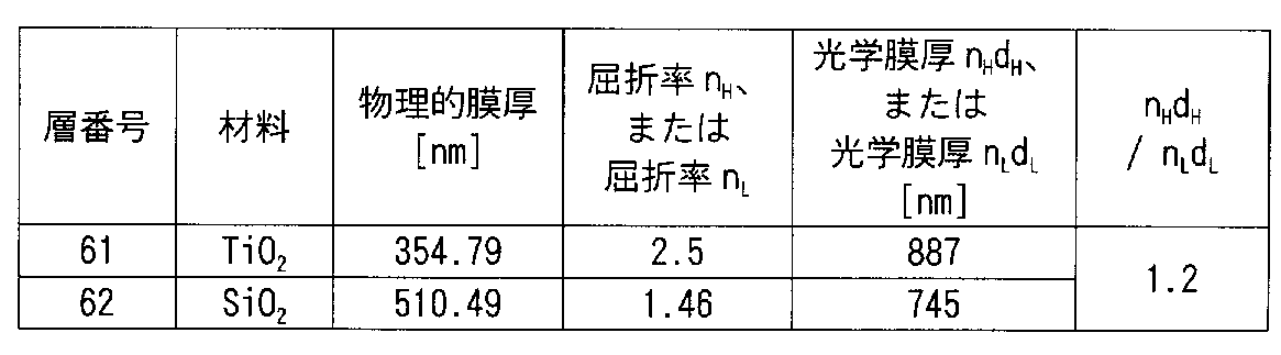
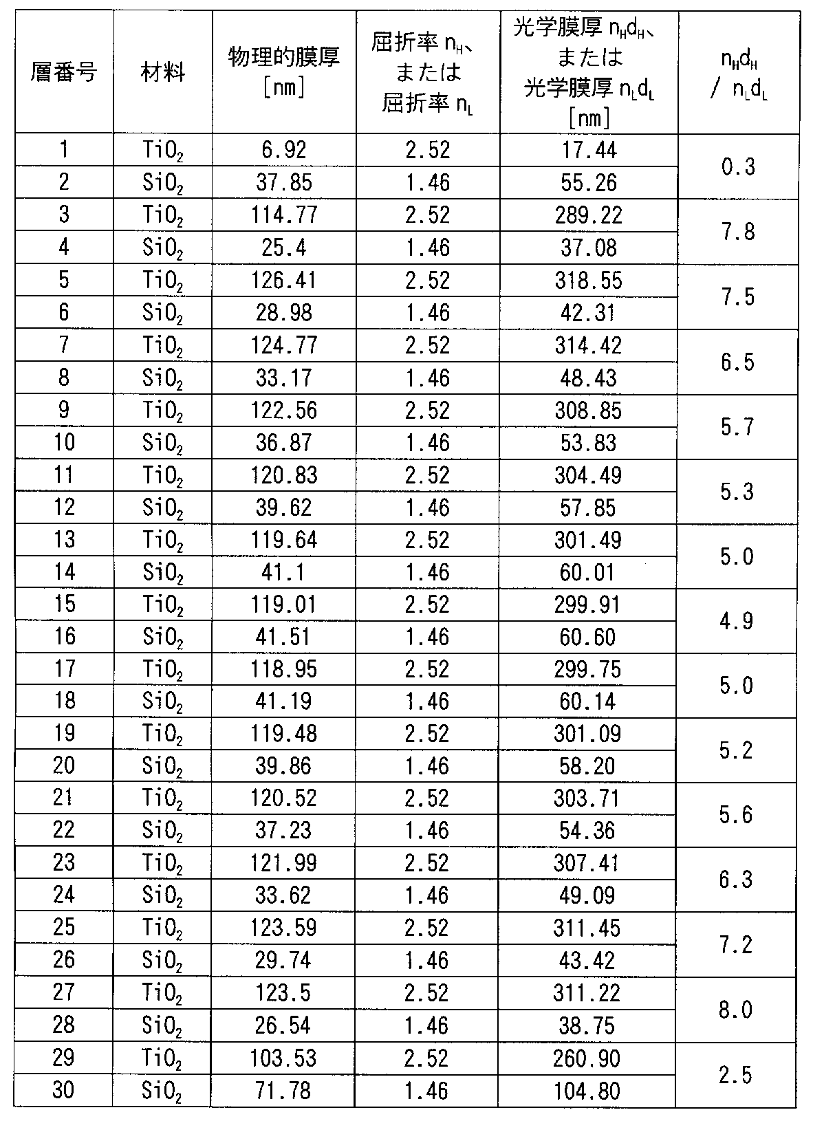
透明基材2としての厚さ1mmのソーダガラス板の一方の表面に、表1~3に示すように高屈折率層31としてのTiO2膜と低屈折率層32としてのSiO2膜とを交互に積層して第1の誘電体多層膜3を形成する。また、該透明基材2の他方の表面に、表4~6に示すように高屈折率層41としてのTiO2膜と低屈折率層42としてのSiO2膜とを交互に積層して第2の誘電体多層膜4を形成し、光学部材1を製造する。
透明基材2としての厚さ1mmのソーダガラス板の一方の表面に、表1~3に示すように高屈折率層31としてのTiO2膜と低屈折率層32としてのSiO2膜とを交互に積層して第1の誘電体多層膜3を形成する。また、該透明基材2の他方の表面に、表4~6に示すように高屈折率層41としてのTiO2膜と低屈折率層42としてのSiO2膜とを交互に積層して第2の誘電体多層膜4を形成し、光学部材1を製造する。
なお、第1の誘電体多層膜3については、高屈折率層31と低屈折率層32とを合わせた全層数は76、すなわち単位屈折率層33の全層数は38、nHdH/nLdL≧3を満足する単位屈折率層33の層数は28、nHdH/nLdL≧5を満足する単位屈折率層33の層数は25、5≦nHdH/nLdL≦8を満足する単位屈折率層33の層数は23、平均nHdH/nLdLは4.8、平均光学膜厚nHdHは232nm、平均光学膜厚nLdLは54nmとする。
第2の誘電体多層膜4については、高屈折率層41と低屈折率層42とを合わせた全層数は90、すなわち単位屈折率層43の全層数は45、平均nHdH/nLdLは1.2、平均光学膜厚nHdHは143nm、平均光学膜厚nLdLは145nmとする。
また、実施例1の光学部材1は、入射角θが0°のときにおいて、350~395nmの範囲における透過率が3%未満、430~630nmの範囲における平均透過率が95%以上、同範囲における最低透過率が90%以上、700~1000nmの範囲における平均透過率が0.1%未満、同範囲における最大透過率が0.5%未満、1000~1100nmの範囲における平均透過率が0.5%未満、同範囲における最大透過率が2%未満を満たし、かつ415±10nmの範囲内および650±6nmの範囲内に透過率が50%となる点を有するものである。


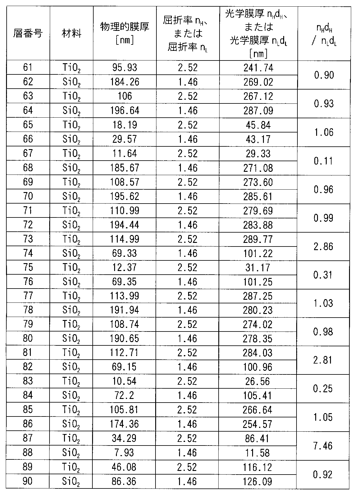
(比較例1)
実施例1で使用したガラス板と同様のガラス板の一方の表面に、表7~9に示すようにTiO2膜とSiO2膜とを交互に積層して赤外波長域遮蔽用の誘電体多層膜を形成する。また、該ガラス板の他方の表面に、実施例1の光学部材1における第2の誘電体多層膜4と同様、表4~6に示すようにTiO2膜とSiO2膜とを交互に積層して紫外線波長域および赤外波長領域遮蔽用の誘電体多層膜を形成し、光学部材を製造する。なお、表7~9に示される赤外波長域遮蔽用の誘電体多層膜は、基本的に各屈折率膜の光学膜厚をλ0/4としたものである。ここで、λ0は反射帯域の中心波長760nmである。
実施例1で使用したガラス板と同様のガラス板の一方の表面に、表7~9に示すようにTiO2膜とSiO2膜とを交互に積層して赤外波長域遮蔽用の誘電体多層膜を形成する。また、該ガラス板の他方の表面に、実施例1の光学部材1における第2の誘電体多層膜4と同様、表4~6に示すようにTiO2膜とSiO2膜とを交互に積層して紫外線波長域および赤外波長領域遮蔽用の誘電体多層膜を形成し、光学部材を製造する。なお、表7~9に示される赤外波長域遮蔽用の誘電体多層膜は、基本的に各屈折率膜の光学膜厚をλ0/4としたものである。ここで、λ0は反射帯域の中心波長760nmである。
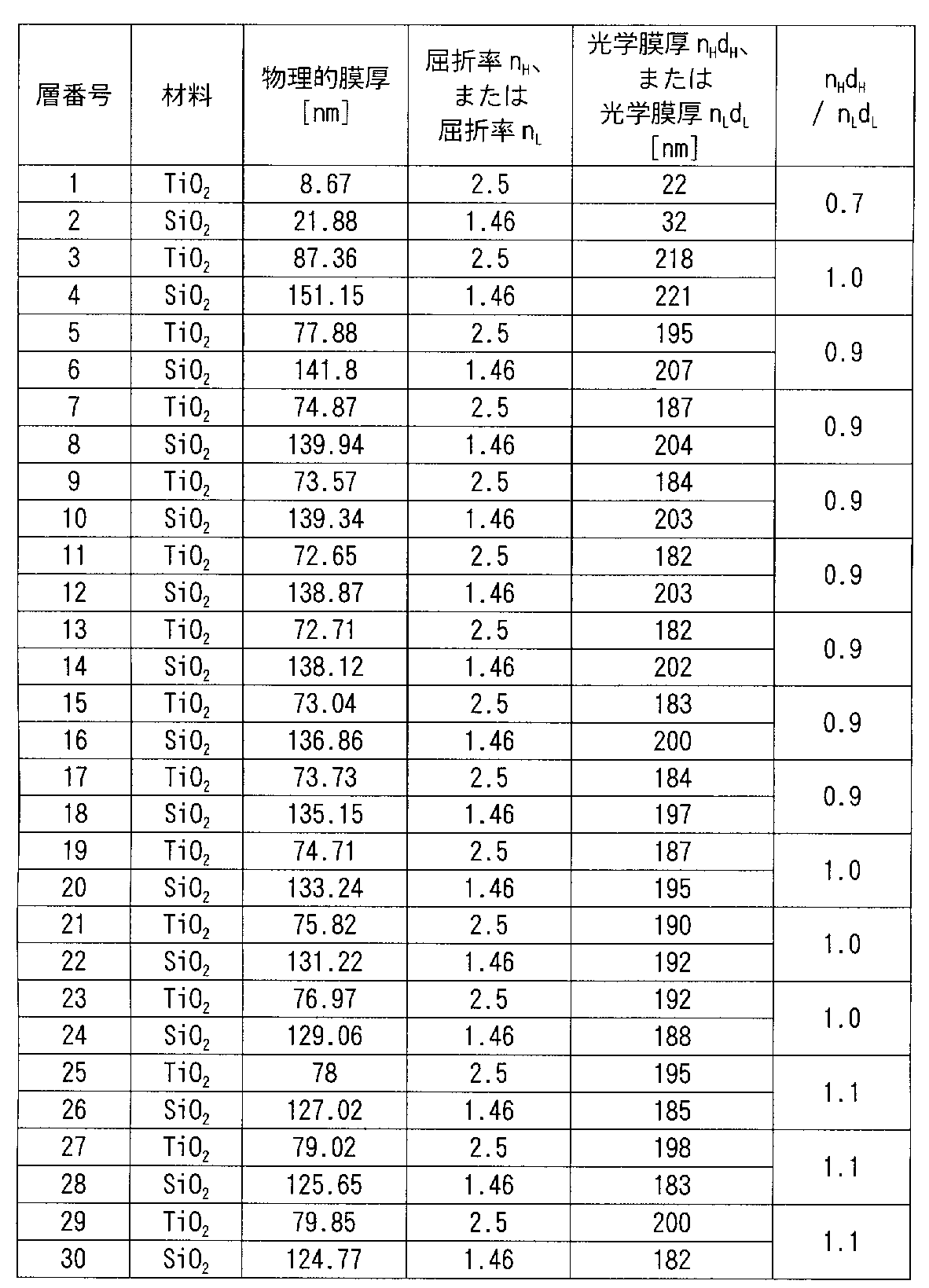
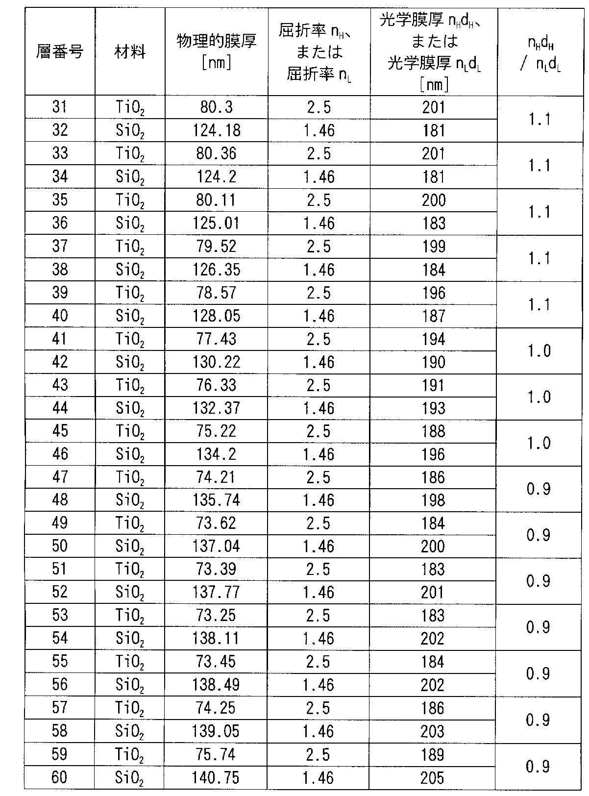
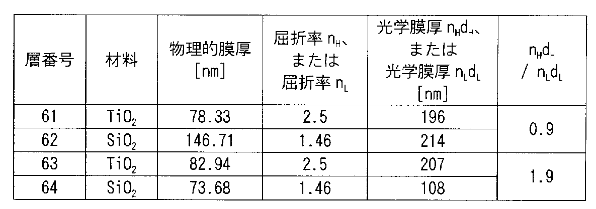
(比較例2)
実施例1で使用したガラス板と同様のガラス板の一方の表面に、表10~12に示すようにTiO2膜とSiO2膜とを交互に積層して赤外波長域遮蔽用の誘電体多層膜を形成する。また、該ガラス板の他方の表面に、実施例1の光学部材1における第2の誘電体多層膜4と同様、表4~6に示すようにTiO2膜とSiO2膜とを交互に積層して紫外線波長域および赤外波長域遮蔽用の誘電体多層膜を形成し、光学部材を製造する。なお、表10~12に示される赤外波長域遮蔽用の誘電体多層膜は、基本的に各屈折率膜の光学膜厚を5λ0/4としたものである。ここで、λ0は反射帯域の中心波長680nmである。
実施例1で使用したガラス板と同様のガラス板の一方の表面に、表10~12に示すようにTiO2膜とSiO2膜とを交互に積層して赤外波長域遮蔽用の誘電体多層膜を形成する。また、該ガラス板の他方の表面に、実施例1の光学部材1における第2の誘電体多層膜4と同様、表4~6に示すようにTiO2膜とSiO2膜とを交互に積層して紫外線波長域および赤外波長域遮蔽用の誘電体多層膜を形成し、光学部材を製造する。なお、表10~12に示される赤外波長域遮蔽用の誘電体多層膜は、基本的に各屈折率膜の光学膜厚を5λ0/4としたものである。ここで、λ0は反射帯域の中心波長680nmである。


次に、実施例1、比較例1、2の光学部材について、光学シミュレーションにより、入射角θが0°のときの分光透過率、および入射角θが30°のときの分光透過率を求めた。図4に、実施例1、比較例1、2の光学部材について、600~700nmの波長範囲における入射角θが0°のときの分光透過率、および入射角θが30°のときの分光透過率を示す。また、図5に、実施例1の光学部材について、300~1200nmの波長範囲における入射角θが0°のときの分光透過率、および入射角θが30°のときの分光透過率を示す。なお、前記光学シミュレーションにおいて、高屈折率層の屈折率は、波長依存性を考慮した。
図4からも明らかなように、第1の誘電体多層膜3におけるnHdH/nLdL≧3、好ましくはnHdH/nLdL≧5を満足する単位屈折率層33の層数が10以上、具体的にはnHdH/nLdL≧3を満足する層数が28、nHdH/nLdL≧5を満足する層数が25である実施例1の光学部材1については、650nm付近のカットオフ帯域における入射角θが0°のときの50%透過波長と入射角θが30°のときの50%透過波長との差を16nmとでき、入射角依存性を効果的に低減できる。また、図5から明らかなように、実施例1の光学部材1については、入射角依存性を効果的に低減できるとともに、透過率リップル、すなわち分光透過率の平坦性も効果的に改善できる。
(実施例2)
透明基材2としての厚さ1mmのソーダガラス板の一方の表面に、表13に示すように高屈折率層31としてのTiO2膜と低屈折率層32としてのSiO2膜とを交互に積層して第1の誘電体多層膜3を形成し、光学部材1を製造する。
透明基材2としての厚さ1mmのソーダガラス板の一方の表面に、表13に示すように高屈折率層31としてのTiO2膜と低屈折率層32としてのSiO2膜とを交互に積層して第1の誘電体多層膜3を形成し、光学部材1を製造する。
なお、第1の誘電体多層膜3については、高屈折率層31と低屈折率層32とを合わせた全層数は30、すなわち単位屈折率層33の全層数は15、nHdH/nLdL≧3を満足する単位屈折率層33の層数は13、nHdH/nLdL≧5を満足する単位屈折率層33の層数は12、5≦nHdH/nLdL≦8を満足する単位屈折率層33の層数は12、平均nHdH/nLdLは5.5、平均光学膜厚nHdHは283nm、平均光学膜厚nLdLは48nmとする。
また、実施例2の光学部材1は、入射角θが0°のときにおいて、360~395nmの範囲における透過率が3%未満、430~630nmの範囲における平均透過率が95%以上、同範囲における最低透過率が90%以上、415±10nmの範囲内および650±6nmの範囲内に透過率が50%となる点を有するものである。
次に、実施例2の光学部材1について、光学シミュレーションにより、入射角θが0°のときの分光透過率、および入射角θが30°のときの分光透過率を求めた。図6に、350~1100nmの波長範囲における入射角θが0°のときの分光透過率、および入射角θが30°のときの分光透過率を示す。なお、前記光学シミュレーションにおいて、高屈折率層の屈折率は、波長依存性を考慮した。
図6からも明らかなように、第1の誘電体多層膜3におけるnHdH/nLdL≧3を満足する単位屈折率層33の層数が13、nHdH/nLdL≧5を満足する単位屈折率層33の層数が12であるものについても、650nm付近のカットオフ帯域における入射角θが0°のときの50%透過波長と入射角θが30°のときの50%透過波長との差を16nmにでき、入射角依存性を効果的に低減できる。
(実施例3)
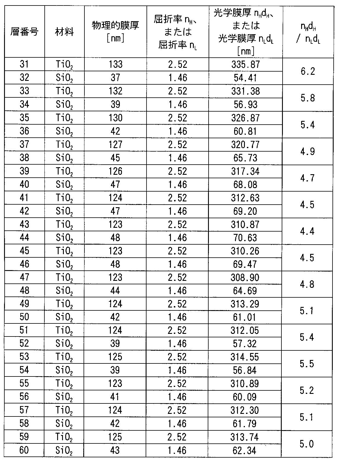
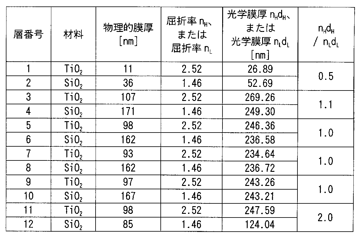
透明基材2としての近赤外線カットフィルタガラス(旭硝子株式会社製NF-50ガラスでガラス厚みは0.3mm)の一方の表面に、表14~16に示すように高屈折率層31としてのTiO2膜と低屈折率層32としてのSiO2膜とを交互に積層して第1の誘電体多層膜3を形成する。また、該透明基材2の他方の表面に、表17に示すように高屈折率層41としてのTiO2膜と低屈折率層42としてのSiO2膜とを交互に積層して第2の誘電体多層膜4を形成し、光学部材1を製造する。
透明基材2としての近赤外線カットフィルタガラス(旭硝子株式会社製NF-50ガラスでガラス厚みは0.3mm)の一方の表面に、表14~16に示すように高屈折率層31としてのTiO2膜と低屈折率層32としてのSiO2膜とを交互に積層して第1の誘電体多層膜3を形成する。また、該透明基材2の他方の表面に、表17に示すように高屈折率層41としてのTiO2膜と低屈折率層42としてのSiO2膜とを交互に積層して第2の誘電体多層膜4を形成し、光学部材1を製造する。
なお、第1の誘電体多層膜3については、高屈折率層31と低屈折率層32とを合わせた全層数は76、すなわち単位屈折率層33の全層数は38、nHdH/nLdL≧3を満足する単位屈折率層33の層数は28、nHdH/nLdL≧5を満足する単位屈折率層33の層数は20、5≦nHdH/nLdL≦8を満足する単位屈折率層33の層数は17、平均nHdH/nLdLは5.1、平均光学膜厚nHdHは247nm、平均光学膜厚nLdLは58nmとする。
第2の誘電体多層膜4については、高屈折率層41と低屈折率層42とを合わせた全層数は12、すなわち単位屈折率層43の全層数は6、平均nHdH/nLdLは1.1、平均光学膜厚nHdHは211nm、平均光学膜厚nLdLは190nmとする。
また、実施例3の光学部材1は、入射角θが0°のときにおいて、350~395nmの範囲における透過率が3%未満、430~545nmの範囲における平均透過率が95%以上、同範囲における最低透過率が90%以上、700~1000nmの範囲における平均透過率が0.1%未満、同範囲における最大透過率が0.5%未満、1000~1100nmの範囲における平均透過率が0.5%未満、同範囲における最大透過率が2%未満を満たし、かつ415±10nmの範囲内および640±6nmの範囲内に透過率が50%となる点を有するものである。


次に、実施例3の光学部材1について、光学シミュレーションにより、入射角θが0°のときの分光透過率、および入射角θが30°のときの分光透過率を求めた。図7に、400~1100nmの波長範囲における入射角θが0°のときの分光透過率、および入射角θが30°のときの分光透過率を示す。なお、前記光学シミュレーションにおいて、各屈折率層の屈折率は、波長依存性を考慮していない。
図7からも明らかなように、透明基材2を変更した実施例3の光学部材1についても、カットオフ帯域における入射角θが0°のときの50%透過波長638nmに対して入射角θが30°のときの50%透過波長を635nmにでき、また同カットオフ帯域における入射角θが0°のときの20%透過波長686nmに対して入射角θが30°のときの20%透過波長を671nmにでき、入射角依存性を効果的に低減できる。
(比較例3)
実施例1で使用したガラス板と同様のガラス板の一方の表面に、表18、19に示すように主としてTiO2膜とAl2O3膜とを交互に積層して赤外波長域遮蔽用の誘電体多層膜を形成する。なお、層番号の1、2、35に記載される膜は調整層であり、層番号の3~34からなる膜が赤外波長域遮蔽用の誘電体多層膜である。また、該ガラス板の他方の表面に、実施例1の光学部材1における第2の誘電体多層膜4と同様、表4~6に示すようにTiO2膜とSiO2膜とを交互に積層して紫外線波長域および赤外波長域遮蔽用の誘電体多層膜を形成し、光学部材を製造する。なお、表18、19に示される赤外波長域遮蔽用の誘電体多層膜は、高屈折率層と中屈折率層(屈折率が1.6を超え、2未満の構成材料からなる)との繰り返し構成である。
実施例1で使用したガラス板と同様のガラス板の一方の表面に、表18、19に示すように主としてTiO2膜とAl2O3膜とを交互に積層して赤外波長域遮蔽用の誘電体多層膜を形成する。なお、層番号の1、2、35に記載される膜は調整層であり、層番号の3~34からなる膜が赤外波長域遮蔽用の誘電体多層膜である。また、該ガラス板の他方の表面に、実施例1の光学部材1における第2の誘電体多層膜4と同様、表4~6に示すようにTiO2膜とSiO2膜とを交互に積層して紫外線波長域および赤外波長域遮蔽用の誘電体多層膜を形成し、光学部材を製造する。なお、表18、19に示される赤外波長域遮蔽用の誘電体多層膜は、高屈折率層と中屈折率層(屈折率が1.6を超え、2未満の構成材料からなる)との繰り返し構成である。


(比較例4)
実施例1で使用したガラス板と同様のガラス板の一方の表面に、表18、19に示すように比較例3と同様のTiO2膜とAl2O3膜とを交互に積層して赤外波長域遮蔽用の誘電体多層膜を形成する。なお、比較例3との相違点は、ガラス板の他方の表面に誘電体多層膜を形成していないことである。
実施例1で使用したガラス板と同様のガラス板の一方の表面に、表18、19に示すように比較例3と同様のTiO2膜とAl2O3膜とを交互に積層して赤外波長域遮蔽用の誘電体多層膜を形成する。なお、比較例3との相違点は、ガラス板の他方の表面に誘電体多層膜を形成していないことである。
次に、比較例3、4の光学部材1について、光学シミュレーションにより、入射角θが0°のときの分光透過率、および入射角θが30°のときの分光透過率を求めた。図8および図9に、300~1300nmの波長範囲における入射角θが0°のときの分光透過率、および入射角θが30°のときの分光透過率を示す。なお、前記光学シミュレーションにおいて、各屈折率層の屈折率は、波長依存性を考慮している。
図8および図9からも明らかなように、本発明を満足しない光学部材については、650nm付近のカットオフ帯域における入射角θが0°のときの50%透過波長と入射角θが30°のときの50%透過波長との差が22nmと大きく、入射角依存性を低減することができない。
(実施例4)
透明基材2としての厚さ1mmのソーダガラス板の一方の表面に、表20、21に示すように高屈折率層31としてのTiO2膜と低屈折率層32としてのSiO2膜とを交互に積層して第1の誘電体多層膜3を形成し、光学部材1を製造する。
透明基材2としての厚さ1mmのソーダガラス板の一方の表面に、表20、21に示すように高屈折率層31としてのTiO2膜と低屈折率層32としてのSiO2膜とを交互に積層して第1の誘電体多層膜3を形成し、光学部材1を製造する。
なお、第1の誘電体多層膜3については、高屈折率層31と低屈折率層32とを合わせた全層数は42、すなわち単位屈折率層33の全層数は21、nHdH/nLdL≧3を満足する単位屈折率層33の層数は13、nHdH/nLdL≧5を満足する単位屈折率層33の層数は13、5≦nHdH/nLdL≦8を満足する単位屈折率層33の層数は8、平均nHdH/nLdLは5.2、平均光学膜厚nHdHは99.4nm、平均光学膜厚nLdLは75.8nmとする。
また、第1の誘電体多層膜3の層番号1~10及び29~42は調整部としても機能する。該調整部は、該調整部に含まれる高屈折率層31の平均光学膜厚をTH、該調整部に含まれる低屈折率層32の平均光学膜厚をTLとしたとき、TH/TLが0.87である。
また、実施例4の光学部材1は、入射角θが0°のときにおいて、360~395nmの範囲における透過率が3%未満、430~630nmの範囲における平均透過率が95%以上、同範囲における最低透過率が90%以上、415±10nmの範囲内、具体的には415~416nmの範囲内、および650±15nmの範囲内、具体的には660~661nmの範囲内に透過率が50%となる点を有するものである。


次に、実施例4の光学部材1について、光学シミュレーションにより、入射角θが0°のときの分光透過率、および入射角θが30°のときの分光透過率を求めた。図10に、350~1100nmの波長範囲における入射角θが0°のときの分光透過率、および入射角θが30°のときの分光透過率を示す。なお、前記光学シミュレーションにおいて、各屈折率層の屈折率は、波長依存性を考慮している。
図10からも明らかなように、第1の誘電体多層膜3におけるnHdH/nLdL≧3を満足する単位屈折率層33の層数が13、nHdH/nLdL≧5を満足する単位屈折率層33の層数が13であるものについても、650nm付近のカットオフ帯域における入射角θが0°のときの50%透過波長と入射角θが30°のときの50%透過波長との差を8nmにでき、入射角依存性を効果的に低減できる。
これは、第1の誘電体多層膜3の一部を調整部として用いたことにより、650nm付近のカットオフ帯域における入射角θが0°と入射角θが30°との波形シフトが平行とならず、波形が変形していることに起因していると考えられる。具体的には、図10に示すとおり、近赤外側の透過率が50~90%となる波長領域において、この範囲における入射角θが0°から30°に変化した場合の波長シフト量は10nm以下であり、波長シフト量が非常に小さいことがわかる。また、近赤外線の透過率が50%未満となる波長領域は、前記透過率が50~90%となる波長領域の波長シフト量と比べ、波長シフト量が大きい。よって、第1の誘電体多層膜3の一部を調整部とすることで、近赤外側の入射角に依存する波長シフト量を不均一化させ、赤色域の波長範囲の入射角依存性を小さくすることができる。
1…光学部材、2…透明基材、3…第1の誘電体多層膜、4…第2の誘電体多層膜、31…高屈折率層、32…低屈折率層、41…高屈折率層、42…低屈折率層、50…撮像装置、51…固体撮像素子、52…カバーガラス、53…レンズ群、54…絞り、55…筐体。
Claims (11)
- 透明基材と、前記透明基材に形成され、屈折率が2以上の高屈折率層と屈折率が1.6以下の低屈折率層とからなる単位屈折率層が複数積層された誘電体多層膜とを有する光学部材であって、
前記誘電体多層膜における前記単位屈折率層の全層数が15以上、かつ前記単位屈折率層における前記高屈折率層の光学膜厚をnHdH、前記低屈折率層の光学膜厚をnLdLとしたとき、前記誘電体多層膜におけるnHdH/nLdL≧3を満足する単位屈折率層の層数が10以上であることを特徴とする光学部材。 - 前記誘電体多層膜における前記単位屈折率層の全層数が15以上、かつ前記誘電体多層膜における前記nHdH/nLdL≧5を満足する単位屈折率層の層数が10以上である請求項1記載の光学部材。
- 前記誘電体多層膜における前記単位屈折率層の全層数が30以上、かつ前記誘電体多層膜における前記nHdH/nLdL≧5を満足する単位屈折率層の層数が15以上である請求項2記載の光学部材。
- 前記誘電体多層膜における前記単位屈折率層の全体におけるnHdH/nLdLの平均値である平均nHdH/nLdLが4.5~5.3である請求項2または3記載の光学部材。
- 前記誘電体多層膜は、前記高屈折率層および前記低屈折率層の一部から構成される合計層数が10層以上の調整部を有するものであって、前記調整部は、前記調整部に含まれる前記高屈折率層の平均光学膜厚をTH、前記調整部に含まれる前記低屈折率層の平均光学膜厚をTLとしたとき、TH/TLが1.5以下であることを特徴とする請求項1乃至4のいずれか1項記載の光学部材。
- 透過帯域と反射帯域との間のカットオフ帯域における入射角0°における50%透過波長と入射角30°における50%透過波長との差が20nm以下である請求項1乃至5のいずれか1項記載の光学部材。
- 前記高屈折率層は、TiO2、Nb2O5、Ta2O5、およびこれらの複合酸化物から選ばれる1種からなり、前記低屈折率層は、SiO2、MgF2、およびこれらの複合酸化物から選ばれる1種からなる請求項1乃至6のいずれか1項記載の光学部材。
- 前記透明基材は板状である請求項1乃至7のいずれか1項記載の光学部材。
- 前記透明基材はレンズ状である請求項1乃至8のいずれか1項記載の光学部材。
- 前記透明基材は赤外波長域に吸収を有する請求項1乃至9のいずれか1項記載の光学部材。
- 視感度補正フィルタとして用いられることを特徴とする請求項1乃至10のいずれか1項記載の光学部材。
Priority Applications (3)
| Application Number | Priority Date | Filing Date | Title |
|---|---|---|---|
| CN201280037552.9A CN103718070B (zh) | 2011-07-28 | 2012-07-25 | 光学部件 |
| JP2013525735A JP6034785B2 (ja) | 2011-07-28 | 2012-07-25 | 光学部材 |
| US14/166,080 US9322965B2 (en) | 2011-07-28 | 2014-01-28 | Optical member |
Applications Claiming Priority (2)
| Application Number | Priority Date | Filing Date | Title |
|---|---|---|---|
| JP2011-165942 | 2011-07-28 | ||
| JP2011165942 | 2011-07-28 |
Related Child Applications (1)
| Application Number | Title | Priority Date | Filing Date |
|---|---|---|---|
| US14/166,080 Continuation US9322965B2 (en) | 2011-07-28 | 2014-01-28 | Optical member |
Publications (1)
| Publication Number | Publication Date |
|---|---|
| WO2013015303A1 true WO2013015303A1 (ja) | 2013-01-31 |
Family
ID=47601144
Family Applications (1)
| Application Number | Title | Priority Date | Filing Date |
|---|---|---|---|
| PCT/JP2012/068794 Ceased WO2013015303A1 (ja) | 2011-07-28 | 2012-07-25 | 光学部材 |
Country Status (4)
| Country | Link |
|---|---|
| US (1) | US9322965B2 (ja) |
| JP (1) | JP6034785B2 (ja) |
| CN (1) | CN103718070B (ja) |
| WO (1) | WO2013015303A1 (ja) |
Cited By (17)
| Publication number | Priority date | Publication date | Assignee | Title |
|---|---|---|---|---|
| JP2013178338A (ja) * | 2012-02-28 | 2013-09-09 | Asahi Glass Co Ltd | 近赤外線カットフィルター |
| JP5617063B1 (ja) * | 2012-12-28 | 2014-10-29 | 旭硝子株式会社 | 近赤外線カットフィルタ |
| JP2014215576A (ja) * | 2013-04-30 | 2014-11-17 | 東海光学株式会社 | 赤外線カットフィルター |
| WO2014199991A1 (ja) * | 2013-06-11 | 2014-12-18 | 日本電気硝子株式会社 | カバー部材、表示装置及びカバー部材の製造方法 |
| JP2015011319A (ja) * | 2013-07-02 | 2015-01-19 | 旭硝子株式会社 | 近赤外線カットフィルタ |
| JP2015011333A (ja) * | 2013-07-02 | 2015-01-19 | 光伸光学工業株式会社 | Irカットフィルタ |
| JP2015045821A (ja) * | 2013-08-29 | 2015-03-12 | 旭硝子株式会社 | 波長選択光学フィルタ |
| CN104516038A (zh) * | 2013-09-30 | 2015-04-15 | 鸿富锦精密工业(深圳)有限公司 | 红外截止滤光片 |
| CN104597537A (zh) * | 2013-10-30 | 2015-05-06 | 日本电波工业株式会社 | 光学零件 |
| US20150160386A1 (en) * | 2012-08-29 | 2015-06-11 | Asahi Glass Company, Limited | Near-infrared cut filter |
| JP2016070965A (ja) * | 2014-09-26 | 2016-05-09 | 旭硝子株式会社 | 近赤外線カットフィルタ |
| JP2016114683A (ja) * | 2014-12-12 | 2016-06-23 | 日本放送協会 | フィルタ及び撮像装置 |
| JP2018006668A (ja) * | 2016-07-07 | 2018-01-11 | 旭硝子株式会社 | 撮像装置 |
| JP2019012121A (ja) * | 2017-06-29 | 2019-01-24 | Agc株式会社 | 光学フィルタおよび撮像装置 |
| US10746908B2 (en) | 2015-09-25 | 2020-08-18 | AGC Inc. | Optical filter and imaging device |
| JP2021009389A (ja) * | 2019-07-02 | 2021-01-28 | エーエーシー オプティックス ソリューションズ ピーティーイー リミテッド | レンズモジュール及び結像システム |
| JP2021184022A (ja) * | 2020-05-21 | 2021-12-02 | Agc株式会社 | 近赤外線カットフィルタ |
Families Citing this family (15)
| Publication number | Priority date | Publication date | Assignee | Title |
|---|---|---|---|---|
| CA2838581A1 (en) | 2011-06-06 | 2012-12-13 | Asahi Glass Company, Limited | Optical filter, solid-state imaging element, imaging device lens and imaging device |
| CN202177716U (zh) * | 2011-07-22 | 2012-03-28 | 浙江水晶光电科技股份有限公司 | 高像素影像系统用滤光片 |
| JP6119747B2 (ja) | 2012-06-04 | 2017-04-26 | 旭硝子株式会社 | 近赤外線カットフィルタ |
| TWI756606B (zh) | 2012-07-16 | 2022-03-01 | 美商唯亞威方案公司 | 光學濾波器及感測器系統 |
| US9989684B2 (en) | 2015-01-23 | 2018-06-05 | Materion Corporation | Near infrared optical interference filters with improved transmission |
| KR102700673B1 (ko) | 2015-02-18 | 2024-08-30 | 마테리온 코포레이션 | 개선된 투과를 갖는 근적외선 광학 간섭 필터 |
| US10555397B2 (en) | 2016-01-28 | 2020-02-04 | Ecosense Lighting Inc. | Systems and methods for providing tunable warm white light |
| JP6767792B2 (ja) * | 2016-07-01 | 2020-10-14 | オリンパス株式会社 | 偏波分離素子、光学系及び光学機器 |
| WO2018083953A1 (ja) * | 2016-11-07 | 2018-05-11 | 東レ株式会社 | 光源ユニット |
| CN106405716B (zh) * | 2016-11-24 | 2018-11-06 | 福建福特科光电股份有限公司 | 消偏振分光片 |
| WO2019006076A1 (en) * | 2017-06-30 | 2019-01-03 | University Of Massachusetts | DEVICES WITH OPTICAL TRANSMISSION AND MANUFACTURE |
| CN108387963B (zh) * | 2018-04-20 | 2021-05-25 | 大连理工大学 | 一种多孔层状结构生色材料及其制备方法 |
| CN110824599B (zh) | 2018-08-14 | 2021-09-03 | 白金科技股份有限公司 | 一种红外带通滤波器 |
| DE102019120668A1 (de) | 2019-07-31 | 2021-02-04 | Leica Camera Aktiengesellschaft | Sensoreinheit |
| CN119148270A (zh) * | 2024-08-21 | 2024-12-17 | 中国科学院上海技术物理研究所 | 一种以硅为基底的宽角度位相差消偏反射镜 |
Citations (7)
| Publication number | Priority date | Publication date | Assignee | Title |
|---|---|---|---|---|
| JPH05207350A (ja) * | 1992-01-24 | 1993-08-13 | Copal Co Ltd | 赤外カットフィルタ付カメラ |
| JPH11101913A (ja) * | 1997-09-29 | 1999-04-13 | Nikon Corp | 光学素子 |
| JP2002040239A (ja) * | 2000-07-26 | 2002-02-06 | Toshiba Lighting & Technology Corp | 光干渉膜構成体およびハロゲン電球 |
| JP2002296414A (ja) * | 2001-01-25 | 2002-10-09 | Canon Inc | 光学素子、それを用いた液晶プロジェクター及びカメラ |
| JP2005114812A (ja) * | 2003-10-03 | 2005-04-28 | Sun Tec Kk | 複合誘電体多層膜フィルタ |
| JP2006285196A (ja) * | 2005-03-11 | 2006-10-19 | Seiko Epson Corp | 光学多層膜、光学素子、反射ミラーおよびプロジェクタ |
| JP2010078714A (ja) * | 2008-09-24 | 2010-04-08 | Panasonic Electric Works Co Ltd | 広域熱線カットフィルタ |
Family Cites Families (8)
| Publication number | Priority date | Publication date | Assignee | Title |
|---|---|---|---|---|
| US4309075A (en) * | 1979-10-05 | 1982-01-05 | Optical Coating Laboratory, Inc. | Multilayer mirror with maximum reflectance |
| US4373782A (en) * | 1980-06-03 | 1983-02-15 | Optical Coating Laboratory, Inc. | Non-polarizing thin film edge filter |
| JPH11202127A (ja) | 1998-01-14 | 1999-07-30 | Canon Inc | ダイクロイックミラー |
| US20070030569A1 (en) * | 2005-08-04 | 2007-02-08 | Guardian Industries Corp. | Broad band antireflection coating and method of making same |
| JP2007183525A (ja) | 2005-12-07 | 2007-07-19 | Murakami Corp | 誘電体多層膜フィルタ |
| JP2008070825A (ja) | 2006-09-15 | 2008-03-27 | Agc Techno Glass Co Ltd | 赤外線遮蔽膜 |
| CN101266309A (zh) * | 2008-04-25 | 2008-09-17 | 同济大学 | 具有宽的低反射旁通带的单峰窄带反射滤光片 |
| WO2011071052A1 (ja) | 2009-12-07 | 2011-06-16 | 旭硝子株式会社 | 光学部材、近赤外線カットフィルタ、固体撮像素子、撮像装置用レンズ、およびそれらを用いた撮像・表示装置 |
-
2012
- 2012-07-25 WO PCT/JP2012/068794 patent/WO2013015303A1/ja not_active Ceased
- 2012-07-25 JP JP2013525735A patent/JP6034785B2/ja active Active
- 2012-07-25 CN CN201280037552.9A patent/CN103718070B/zh active Active
-
2014
- 2014-01-28 US US14/166,080 patent/US9322965B2/en active Active
Patent Citations (7)
| Publication number | Priority date | Publication date | Assignee | Title |
|---|---|---|---|---|
| JPH05207350A (ja) * | 1992-01-24 | 1993-08-13 | Copal Co Ltd | 赤外カットフィルタ付カメラ |
| JPH11101913A (ja) * | 1997-09-29 | 1999-04-13 | Nikon Corp | 光学素子 |
| JP2002040239A (ja) * | 2000-07-26 | 2002-02-06 | Toshiba Lighting & Technology Corp | 光干渉膜構成体およびハロゲン電球 |
| JP2002296414A (ja) * | 2001-01-25 | 2002-10-09 | Canon Inc | 光学素子、それを用いた液晶プロジェクター及びカメラ |
| JP2005114812A (ja) * | 2003-10-03 | 2005-04-28 | Sun Tec Kk | 複合誘電体多層膜フィルタ |
| JP2006285196A (ja) * | 2005-03-11 | 2006-10-19 | Seiko Epson Corp | 光学多層膜、光学素子、反射ミラーおよびプロジェクタ |
| JP2010078714A (ja) * | 2008-09-24 | 2010-04-08 | Panasonic Electric Works Co Ltd | 広域熱線カットフィルタ |
Cited By (22)
| Publication number | Priority date | Publication date | Assignee | Title |
|---|---|---|---|---|
| JP2013178338A (ja) * | 2012-02-28 | 2013-09-09 | Asahi Glass Co Ltd | 近赤外線カットフィルター |
| US20150160386A1 (en) * | 2012-08-29 | 2015-06-11 | Asahi Glass Company, Limited | Near-infrared cut filter |
| US10073202B2 (en) * | 2012-08-29 | 2018-09-11 | Asahi Glass Company, Limited | Near-infrared cut filter |
| JP5617063B1 (ja) * | 2012-12-28 | 2014-10-29 | 旭硝子株式会社 | 近赤外線カットフィルタ |
| JP2014215576A (ja) * | 2013-04-30 | 2014-11-17 | 東海光学株式会社 | 赤外線カットフィルター |
| WO2014199991A1 (ja) * | 2013-06-11 | 2014-12-18 | 日本電気硝子株式会社 | カバー部材、表示装置及びカバー部材の製造方法 |
| JPWO2014199991A1 (ja) * | 2013-06-11 | 2017-02-23 | 日本電気硝子株式会社 | カバー部材、表示装置及びカバー部材の製造方法 |
| JP2015011333A (ja) * | 2013-07-02 | 2015-01-19 | 光伸光学工業株式会社 | Irカットフィルタ |
| JP2015011319A (ja) * | 2013-07-02 | 2015-01-19 | 旭硝子株式会社 | 近赤外線カットフィルタ |
| JP2015045821A (ja) * | 2013-08-29 | 2015-03-12 | 旭硝子株式会社 | 波長選択光学フィルタ |
| CN104516038A (zh) * | 2013-09-30 | 2015-04-15 | 鸿富锦精密工业(深圳)有限公司 | 红外截止滤光片 |
| JP2015111241A (ja) * | 2013-10-30 | 2015-06-18 | 日本電波工業株式会社 | 光学部品 |
| CN104597537A (zh) * | 2013-10-30 | 2015-05-06 | 日本电波工业株式会社 | 光学零件 |
| JP2016070965A (ja) * | 2014-09-26 | 2016-05-09 | 旭硝子株式会社 | 近赤外線カットフィルタ |
| JP2016114683A (ja) * | 2014-12-12 | 2016-06-23 | 日本放送協会 | フィルタ及び撮像装置 |
| US10746908B2 (en) | 2015-09-25 | 2020-08-18 | AGC Inc. | Optical filter and imaging device |
| JP2018006668A (ja) * | 2016-07-07 | 2018-01-11 | 旭硝子株式会社 | 撮像装置 |
| JP2019012121A (ja) * | 2017-06-29 | 2019-01-24 | Agc株式会社 | 光学フィルタおよび撮像装置 |
| JP2021140177A (ja) * | 2017-06-29 | 2021-09-16 | Agc株式会社 | 光学フィルタおよび撮像装置 |
| JP2021009389A (ja) * | 2019-07-02 | 2021-01-28 | エーエーシー オプティックス ソリューションズ ピーティーイー リミテッド | レンズモジュール及び結像システム |
| JP2021184022A (ja) * | 2020-05-21 | 2021-12-02 | Agc株式会社 | 近赤外線カットフィルタ |
| JP7491052B2 (ja) | 2020-05-21 | 2024-05-28 | Agc株式会社 | 近赤外線カットフィルタ |
Also Published As
| Publication number | Publication date |
|---|---|
| US9322965B2 (en) | 2016-04-26 |
| CN103718070A (zh) | 2014-04-09 |
| JP6034785B2 (ja) | 2016-11-30 |
| CN103718070B (zh) | 2016-09-07 |
| JPWO2013015303A1 (ja) | 2015-02-23 |
| US20140139912A1 (en) | 2014-05-22 |
Similar Documents
| Publication | Publication Date | Title |
|---|---|---|
| JP6034785B2 (ja) | 光学部材 | |
| CN107255841B (zh) | 近红外线截止滤波器 | |
| JP5617063B1 (ja) | 近赤外線カットフィルタ | |
| JP6003895B2 (ja) | 近赤外線カットフィルター | |
| KR101674036B1 (ko) | 광학 필터 | |
| US9726797B2 (en) | Near-infrared cut filter | |
| JP5973747B2 (ja) | 近赤外線カットフィルター | |
| WO2014034386A1 (ja) | 近赤外線カットフィルタ | |
| JP6383980B2 (ja) | 近赤外線カットフィルタ | |
| JP2004354735A (ja) | 光線カットフィルタ | |
| JP6136661B2 (ja) | 近赤外線カットフィルタ | |
| JP5287362B2 (ja) | 光学フィルタおよび撮像システム |
Legal Events
| Date | Code | Title | Description |
|---|---|---|---|
| 121 | Ep: the epo has been informed by wipo that ep was designated in this application |
Ref document number: 12817903 Country of ref document: EP Kind code of ref document: A1 |
|
| ENP | Entry into the national phase |
Ref document number: 2013525735 Country of ref document: JP Kind code of ref document: A |
|
| NENP | Non-entry into the national phase |
Ref country code: DE |
|
| 122 | Ep: pct application non-entry in european phase |
Ref document number: 12817903 Country of ref document: EP Kind code of ref document: A1 |