WO2013005488A1 - 発光装置および表示装置 - Google Patents
発光装置および表示装置 Download PDFInfo
- Publication number
- WO2013005488A1 WO2013005488A1 PCT/JP2012/063053 JP2012063053W WO2013005488A1 WO 2013005488 A1 WO2013005488 A1 WO 2013005488A1 JP 2012063053 W JP2012063053 W JP 2012063053W WO 2013005488 A1 WO2013005488 A1 WO 2013005488A1
- Authority
- WO
- WIPO (PCT)
- Prior art keywords
- reflection
- light
- total reflectance
- light emitting
- region
- Prior art date
- Legal status (The legal status is an assumption and is not a legal conclusion. Google has not performed a legal analysis and makes no representation as to the accuracy of the status listed.)
- Ceased
Links
Images






Classifications
-
- F—MECHANICAL ENGINEERING; LIGHTING; HEATING; WEAPONS; BLASTING
- F21—LIGHTING
- F21V—FUNCTIONAL FEATURES OR DETAILS OF LIGHTING DEVICES OR SYSTEMS THEREOF; STRUCTURAL COMBINATIONS OF LIGHTING DEVICES WITH OTHER ARTICLES, NOT OTHERWISE PROVIDED FOR
- F21V5/00—Refractors for light sources
- F21V5/04—Refractors for light sources of lens shape
-
- F—MECHANICAL ENGINEERING; LIGHTING; HEATING; WEAPONS; BLASTING
- F21—LIGHTING
- F21V—FUNCTIONAL FEATURES OR DETAILS OF LIGHTING DEVICES OR SYSTEMS THEREOF; STRUCTURAL COMBINATIONS OF LIGHTING DEVICES WITH OTHER ARTICLES, NOT OTHERWISE PROVIDED FOR
- F21V7/00—Reflectors for light sources
-
- F—MECHANICAL ENGINEERING; LIGHTING; HEATING; WEAPONS; BLASTING
- F21—LIGHTING
- F21V—FUNCTIONAL FEATURES OR DETAILS OF LIGHTING DEVICES OR SYSTEMS THEREOF; STRUCTURAL COMBINATIONS OF LIGHTING DEVICES WITH OTHER ARTICLES, NOT OTHERWISE PROVIDED FOR
- F21V7/00—Reflectors for light sources
- F21V7/0091—Reflectors for light sources using total internal reflection
-
- G—PHYSICS
- G02—OPTICS
- G02F—OPTICAL DEVICES OR ARRANGEMENTS FOR THE CONTROL OF LIGHT BY MODIFICATION OF THE OPTICAL PROPERTIES OF THE MEDIA OF THE ELEMENTS INVOLVED THEREIN; NON-LINEAR OPTICS; FREQUENCY-CHANGING OF LIGHT; OPTICAL LOGIC ELEMENTS; OPTICAL ANALOGUE/DIGITAL CONVERTERS
- G02F1/00—Devices or arrangements for the control of the intensity, colour, phase, polarisation or direction of light arriving from an independent light source, e.g. switching, gating or modulating; Non-linear optics
- G02F1/01—Devices or arrangements for the control of the intensity, colour, phase, polarisation or direction of light arriving from an independent light source, e.g. switching, gating or modulating; Non-linear optics for the control of the intensity, phase, polarisation or colour
- G02F1/13—Devices or arrangements for the control of the intensity, colour, phase, polarisation or direction of light arriving from an independent light source, e.g. switching, gating or modulating; Non-linear optics for the control of the intensity, phase, polarisation or colour based on liquid crystals, e.g. single liquid crystal display cells
- G02F1/133—Constructional arrangements; Operation of liquid crystal cells; Circuit arrangements
- G02F1/1333—Constructional arrangements; Manufacturing methods
- G02F1/1335—Structural association of cells with optical devices, e.g. polarisers or reflectors
- G02F1/1336—Illuminating devices
- G02F1/133602—Direct backlight
- G02F1/133603—Direct backlight with LEDs
-
- G—PHYSICS
- G02—OPTICS
- G02F—OPTICAL DEVICES OR ARRANGEMENTS FOR THE CONTROL OF LIGHT BY MODIFICATION OF THE OPTICAL PROPERTIES OF THE MEDIA OF THE ELEMENTS INVOLVED THEREIN; NON-LINEAR OPTICS; FREQUENCY-CHANGING OF LIGHT; OPTICAL LOGIC ELEMENTS; OPTICAL ANALOGUE/DIGITAL CONVERTERS
- G02F1/00—Devices or arrangements for the control of the intensity, colour, phase, polarisation or direction of light arriving from an independent light source, e.g. switching, gating or modulating; Non-linear optics
- G02F1/01—Devices or arrangements for the control of the intensity, colour, phase, polarisation or direction of light arriving from an independent light source, e.g. switching, gating or modulating; Non-linear optics for the control of the intensity, phase, polarisation or colour
- G02F1/13—Devices or arrangements for the control of the intensity, colour, phase, polarisation or direction of light arriving from an independent light source, e.g. switching, gating or modulating; Non-linear optics for the control of the intensity, phase, polarisation or colour based on liquid crystals, e.g. single liquid crystal display cells
- G02F1/133—Constructional arrangements; Operation of liquid crystal cells; Circuit arrangements
- G02F1/1333—Constructional arrangements; Manufacturing methods
- G02F1/1335—Structural association of cells with optical devices, e.g. polarisers or reflectors
- G02F1/1336—Illuminating devices
- G02F1/133602—Direct backlight
- G02F1/133605—Direct backlight including specially adapted reflectors
-
- F—MECHANICAL ENGINEERING; LIGHTING; HEATING; WEAPONS; BLASTING
- F21—LIGHTING
- F21Y—INDEXING SCHEME ASSOCIATED WITH SUBCLASSES F21K, F21L, F21S and F21V, RELATING TO THE FORM OR THE KIND OF THE LIGHT SOURCES OR OF THE COLOUR OF THE LIGHT EMITTED
- F21Y2101/00—Point-like light sources
-
- F—MECHANICAL ENGINEERING; LIGHTING; HEATING; WEAPONS; BLASTING
- F21—LIGHTING
- F21Y—INDEXING SCHEME ASSOCIATED WITH SUBCLASSES F21K, F21L, F21S and F21V, RELATING TO THE FORM OR THE KIND OF THE LIGHT SOURCES OR OF THE COLOUR OF THE LIGHT EMITTED
- F21Y2115/00—Light-generating elements of semiconductor light sources
- F21Y2115/10—Light-emitting diodes [LED]
-
- H—ELECTRICITY
- H10—SEMICONDUCTOR DEVICES; ELECTRIC SOLID-STATE DEVICES NOT OTHERWISE PROVIDED FOR
- H10H—INORGANIC LIGHT-EMITTING SEMICONDUCTOR DEVICES HAVING POTENTIAL BARRIERS
- H10H20/00—Individual inorganic light-emitting semiconductor devices having potential barriers, e.g. light-emitting diodes [LED]
- H10H20/80—Constructional details
- H10H20/85—Packages
- H10H20/855—Optical field-shaping means, e.g. lenses
- H10H20/856—Reflecting means
-
- H—ELECTRICITY
- H10—SEMICONDUCTOR DEVICES; ELECTRIC SOLID-STATE DEVICES NOT OTHERWISE PROVIDED FOR
- H10W—GENERIC PACKAGES, INTERCONNECTIONS, CONNECTORS OR OTHER CONSTRUCTIONAL DETAILS OF DEVICES COVERED BY CLASS H10
- H10W72/00—Interconnections or connectors in packages
- H10W72/851—Dispositions of multiple connectors or interconnections
- H10W72/874—On different surfaces
- H10W72/884—Die-attach connectors and bond wires
-
- H—ELECTRICITY
- H10—SEMICONDUCTOR DEVICES; ELECTRIC SOLID-STATE DEVICES NOT OTHERWISE PROVIDED FOR
- H10W—GENERIC PACKAGES, INTERCONNECTIONS, CONNECTORS OR OTHER CONSTRUCTIONAL DETAILS OF DEVICES COVERED BY CLASS H10
- H10W74/00—Encapsulations, e.g. protective coatings
Definitions
- the present invention relates to a light emitting device provided in a backlight unit that irradiates light on the back surface of a display panel, and a display device including the light emitting device.
- liquid crystal is sealed between two transparent substrates, and when a voltage is applied, the orientation of the liquid crystal molecules is changed and the light transmittance is changed to optically display a predetermined image or the like. Is done.
- the liquid crystal itself is not a light emitter.
- the back side of a transmissive display panel is irradiated with light using a cold cathode tube (CCFL), a light emitting diode (LED) as a light source, or the like.
- CCFL cold cathode tube
- LED light emitting diode
- a backlight unit is provided.
- light sources such as cold-cathode tubes and LEDs are arranged on the bottom surface to emit light
- light sources such as cold-cathode tubes and LEDs are arranged on the edge of a transparent plate called a light guide plate.
- a transparent plate called a light guide plate.
- LEDs have excellent characteristics such as low power consumption, long life, and reduced environmental impact by not using mercury, but they are expensive in price, and until the blue LED is invented, the white LED is The use of the backlight unit as a light source was delayed due to the absence of light and the higher directivity. However, in recent years, high color rendering high-intensity white LEDs are rapidly spreading in lighting applications, and the LEDs are becoming cheaper accordingly. Therefore, as a light source of a backlight unit, a transition from a cold cathode tube to an LED is performed. Is progressing.
- the edge light type is more effective than the direct type from the viewpoint of irradiating light with uniform brightness in the surface direction on the back surface of the display panel.
- the edge light type backlight unit has a problem that heat generated by the light source is concentrated due to the light source being concentrated on the edge portion of the light guide plate, and the bezel portion of the display panel is enlarged. Arise.
- the edge light type backlight unit has a great restriction on partial dimming control (local dimming), which is attracting attention as a control method capable of improving the quality and power saving of a display image. There is a problem that it is not possible to control a small divided area where high quality and power saving can be achieved.
- the luminance of the irradiated object is in the plane direction of the irradiated object. Studies are being conducted on a method capable of irradiating the display panel with light so as to be uniform.
- Patent Document 1 discloses an inverted cone light emission including a light emitting element, a resin lens having an inverted conical recess provided so as to cover the light emitting element, and a reflecting plate provided around the resin lens.
- An element lamp is disclosed.
- Patent Document 2 discloses a light source unit that includes a light emitting element and a light guide reflector that guides light while reflecting light emitted from the light emitting element in a direction orthogonal to the optical axis.
- the light emitting element is provided at the center of the bottom of the reflecting plate, the outer shape of the reflecting plate is square, and the side wall of the reflecting plate is perpendicular to the bottom of the reflecting plate. Is provided.
- the outer shape of the reflector is a polygonal shape, the distance from the light emitting element to the polygonal corner is longer than the distance to the side, and as a result, the portion of the display panel that faces the corner The amount of light applied is smaller than the amount of light applied to the portion facing the side, and the amount of light applied to the display panel becomes non-uniform.
- An object of the present invention is to irradiate a display panel with light so that the luminance of the display panel is uniform in the surface direction of the display panel in a light emitting device used in a backlight unit of the display device including the display panel. It is possible to provide a light-emitting device that can be thinned and a display device including the light-emitting device.
- the present invention is a light emitting device for irradiating an irradiated object, A light emitting unit for irradiating the irradiated body with light; A reflective member provided around the light emitting unit, The reflective member is The outer shape when viewed in plan from the irradiated body side is a polygonal shape, When viewed in plan from the irradiated body side, the average total reflectance in the corner portion of the reflecting member and the first reflecting region that is the region between the corner portion and the light emitting portion is the side of the reflecting member.
- the light emitting unit is a light emitting device characterized in that the light emitting unit is disposed in a central portion of the reflecting member when viewed in plan from the irradiated body side.
- the reflecting member is In the first reflection region, having a first reference reflection portion having a predetermined total reflectance, and a high reflection portion having a total reflectance higher than the predetermined total reflectance,
- the total reflectance of the corner portion, the side portion, and the second reflection region is preferably equal to the predetermined total reflectance.
- the reflecting member is In the second reflection region, having a second reference reflection part having a predetermined total reflectance, and a first low reflection part having a total reflectance lower than the predetermined total reflectance,
- the total reflectance of the corner portion, the side portion, and the first reflection region is preferably equal to the predetermined total reflectance.
- the reflecting member is In the side, having a third reference reflection portion having a predetermined total reflectance, and a second low reflection portion having a total reflectance lower than the predetermined total reflectance,
- the total reflectance of the corner portion, the first reflection region, and the second reflection region is preferably equal to the predetermined total reflectance.
- the reflecting member is In the first reflection region, having a first reference reflection portion having a predetermined total reflectance, and a high reflection portion having a total reflectance higher than the predetermined total reflectance, In the second reflection region, having a second reference reflection portion having the predetermined total reflectance, and a first low reflection portion having a total reflectance lower than the predetermined total reflectance, It is preferable that the total reflectance of the corner portion and the side portion is equal to the predetermined total reflectance.
- a diffuse reflection range of the high reflection portion is narrower than a diffuse reflection range of the second reflection region.
- a diffuse reflection range of the first low reflection portion is wider than a diffuse reflection range of the first reflection region.
- a diffuse reflection range of the second low reflection portion is wider than a diffuse reflection range of the first reflection region.
- the diffuse reflection range of the high reflection portion is narrower than the diffuse reflection range of the first reference reflection portion
- the diffuse reflection range of the first low reflection portion is wider than the diffuse reflection range of the first reference reflection portion
- the diffuse reflection range of the second reference reflection portion is equal to the diffuse reflection range of the first reference reflection portion.
- the reflecting member has a base portion that surrounds the light emitting element, and an inclined portion that surrounds the base portion and is inclined so as to approach the irradiated body as the distance from the light emitting element increases.
- the present invention also provides a display panel, And a lighting device including the light emitting device for irradiating light on the back surface of the display panel.
- the reflecting member has a larger average total reflectance in the corner portion and the first reflecting region than in the average total reflectance in the side portion and the second reflecting region.
- the ratio of the amount of light that is reflected at the first reflection region and the corners and reaches the irradiated body to the amount of light that is reflected at the two reflective regions and the side and reaches the irradiated body is increased as compared with the conventional case. . That is, the ratio of the amount of light reaching the portion facing the corner portion of the reflecting member in the irradiated body to the amount of light reaching the portion facing the side portion of the reflecting member in the irradiated body is increased as compared with the prior art. As a result, the light irradiated to the irradiated object can be made uniform.
- the first reflection region, the corner portion, the side portion, and the high reflection portion having a higher total reflectivity than the total reflectivity of the second reflection region are irradiated by the first reflection region. It is possible to increase the amount of light reaching the portion facing the corner of the reflecting member in the body. Therefore, the ratio of the amount of light reaching the portion facing the corner of the reflecting member in the irradiated body to the amount of light reaching the portion facing the side of the reflecting member in the irradiated body is increased as compared with the conventional case. It is possible to make the light irradiated to the irradiated body uniform.
- the first low reflection portion formed in the second reflection region and having a total reflectance lower than that of the second reference reflection portion, the corner portion, the side portion, and the first reflection region It is possible to reduce the amount of light reaching the portion facing the side of the reflecting member in the irradiated body. Therefore, the ratio of the amount of light reaching the portion facing the corner of the reflecting member in the irradiated body to the amount of light reaching the portion facing the side of the reflecting member in the irradiated body is increased as compared with the conventional case. It is possible to make the light irradiated to the irradiated body uniform.
- the second low reflection formed on the side portion of the reflection member and having a total reflectance lower than the total reflectance of the third reference reflection portion, the corner portion, the first reflection region, and the second reflection region.
- the portion can reduce the amount of light reaching the portion of the irradiated body that faces the side of the reflecting member. Therefore, the ratio of the amount of light reaching the portion facing the corner of the reflecting member in the irradiated body to the amount of light reaching the portion facing the side of the reflecting member in the irradiated body is increased as compared with the conventional case. It is possible to make the light irradiated to the irradiated body uniform.
- the first reflection region, the corner portion, the side portion, and the high reflection portion having a higher total reflectivity than the total reflectivity of the second reflection region are irradiated by the first reflection region.
- the amount of light that reaches the part facing the corner of the reflecting member in the body can be increased and formed in the second reflecting region of the reflecting member, the first reference reflecting part, the second reference reflecting part, the high reflecting part,
- the amount of light reaching the part facing the side part of the reflecting member in the irradiated body can be reduced by the first low reflection part having a total reflectance lower than the total reflectance of the corner part and the side part.
- the ratio of the amount of light reaching the portion facing the corner of the reflecting member in the irradiated body to the amount of light reaching the portion facing the side of the reflecting member in the irradiated body is increased as compared with the conventional case. It is possible to make the light irradiated to the irradiated body uniform.
- the diffuse reflection range of the high reflection portion is narrower than the diffuse reflection range of the second reflection region. That is, the light reflected by the high reflection portion diffuses in a narrower range than the light reflected by the second reflection region. This further increases the ratio of the amount of light reaching the portion facing the corner of the reflecting member in the irradiated body to the amount of light reaching the portion facing the side portion of the reflecting member in the irradiated body. It is possible to make the light irradiated to the irradiated body uniform.
- the diffuse reflection range of the first low reflection portion is wider than the diffuse reflection range of the first reflection region. That is, the light reflected by the first low reflection portion diffuses over a wider range than the light reflected by the first reflection region. This further increases the ratio of the amount of light reaching the portion facing the corner of the reflecting member in the irradiated body to the amount of light reaching the portion facing the side portion of the reflecting member in the irradiated body. It is possible to make the light irradiated to the irradiated body uniform.
- the diffuse reflection range of the second low reflection portion is wider than the diffuse reflection range of the first reflection region. That is, the light reflected by the second low reflection portion diffuses over a wider range than the light reflected by the first reflection region. This further increases the ratio of the amount of light reaching the portion facing the corner of the reflecting member in the irradiated body to the amount of light reaching the portion facing the side portion of the reflecting member in the irradiated body. It is possible to make the light irradiated to the irradiated body uniform.
- the diffuse reflection range of the high reflection part is narrower than the diffuse reflection range of the first reference reflection part, and the diffuse reflection range of the first low reflection part is larger than the diffuse reflection range of the first reference reflection part.
- the diffuse reflection range of the second reference reflection portion is equal to the diffuse reflection range of the first reference reflection portion. That is, the light reflected by the first low reflection part diffuses over a wider range than the light reflected by the high reflection part. This further increases the ratio of the amount of light reaching the portion facing the corner of the reflecting member in the irradiated body to the amount of light reaching the portion facing the side portion of the reflecting member in the irradiated body. It is possible to make the light irradiated to the irradiated body uniform.
- the inclined portion is inclined so as to approach the irradiated body as the distance from the light emitting element increases, so that the light emitted from the light emitting element faces the side of the reflecting member in the irradiated body and It is easy to reach the part facing the corner. Therefore, the light irradiated to the irradiated object can be made uniform.
- the display device emits light to the back surface of the display panel by the illumination device including the light emitting device, so that a higher quality image can be displayed.
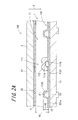
- FIG. 2 is a diagram schematically showing a cross section of the liquid crystal display device when cut along a cutting plane line AA in FIG.
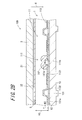
- FIG. 2 is a diagram schematically showing a cross section of the liquid crystal display device when cut along a cutting plane line BB in FIG. 1.
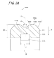
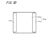
- a base and an LED chip It is a figure which shows a base and an LED chip.
- FIG. 1 is an exploded perspective view showing the configuration of the liquid crystal display device 100 according to the first embodiment of the present invention.
- FIG. 2A is a diagram schematically showing a cross section of the liquid crystal display device 100 when cut along the cutting plane line AA in FIG.
- FIG. 2B is a diagram schematically showing a cross section of the liquid crystal display device 100 taken along the cutting plane line BB in FIG.
- the liquid crystal display device 100 which is a display device of the present invention is a device that displays an image on a display screen by outputting image information in a television receiver or a personal computer.
- the display screen is formed by a liquid crystal panel 2 that is a transmissive display panel having liquid crystal elements, and the liquid crystal panel 2 is formed in a rectangular flat plate shape.
- the liquid crystal panel 2 two surfaces in the thickness direction are a front surface 21 and a back surface 22.
- the liquid crystal display device 100 displays an image so as to be visible when viewed from the front surface 21 toward the rear surface 22.
- the liquid crystal display device 100 includes a liquid crystal panel 2 and a backlight unit 1 including a light emitting device according to the present invention.
- the liquid crystal panel 2 is supported by the side wall portion 132 in parallel with the bottom surface 131a of the bottom portion 131 of the frame member 13 included in the backlight unit 1.
- the liquid crystal panel 2 includes two substrates and is formed in a rectangular plate shape when viewed from the thickness direction.
- the liquid crystal panel 2 is a TFT (thin film) liquid crystal is injected into the gap between the two substrates.
- the liquid crystal panel 2 exhibits a display function by being irradiated with light from the backlight unit 1 disposed on the back surface 22 side as a backlight.
- the two substrates are provided with drivers (source drivers) for driving the pixels in the liquid crystal panel 2, various elements, and wirings.
- a diffusion plate 3 is disposed between the liquid crystal panel 2 and the backlight unit 1 in parallel with the liquid crystal panel 2.
- a prism sheet may be disposed between the liquid crystal panel 2 and the diffusion plate 3.
- the diffusion plate 3 prevents the luminance from being locally biased by diffusing the light emitted from the backlight unit 1 in the surface direction.
- the prism sheet directs the traveling direction of the light reaching from the back surface 22 side through the diffusion plate 3 to the front surface 21 side.
- the traveling direction of light includes a lot of components in the surface direction as vector components.
- the prism sheet converts the traveling direction of light containing a lot of vector components in the surface direction into the traveling direction of light containing many components in the thickness direction.
- the prism sheet is formed with a large number of lens or prism-shaped portions arranged in the plane direction, thereby reducing the diffusion of light traveling in the thickness direction. Therefore, the luminance can be increased in the display by the liquid crystal display device 100.
- the backlight unit 1 is a direct type backlight device that irradiates the liquid crystal panel 2 with light from the back surface 22 side.
- the backlight unit 1 includes a plurality of light emitting devices 11 that irradiate light to the liquid crystal panel 2, a plurality of printed circuit boards 12, and a frame member 13.
- the frame member 13 is a basic structure of the backlight unit 1, and includes a flat plate-like bottom portion 131 that faces the liquid crystal panel 2 at a predetermined interval, and a side wall portion 132 that is connected to the bottom portion 131 and rises from the bottom portion 131.
- the bottom 131 is formed in a rectangular shape when viewed from the thickness direction, and its size is slightly larger than that of the liquid crystal panel 2.
- the side wall part 132 is formed to rise from the two end parts forming the short side of the bottom part 131 and the two end parts forming the long side to the front surface 21 side of the liquid crystal panel 2. As a result, four flat side wall portions 132 are formed around the bottom portion 131.
- the printed circuit board 12 is fixed to the bottom 131 of the frame member 13.
- a plurality of light emitting devices 11 are provided on the printed circuit board 12.
- the printed circuit board 12 is, for example, a substrate made of glass epoxy having conductive layers formed on both sides.
- the plurality of light emitting devices 11 irradiate the liquid crystal panel 2 with light.
- a plurality of printed circuit boards 12 provided with a plurality of light emitting devices 11 are disposed so as to face the entire back surface 22 of the liquid crystal panel 2 through the diffusion plate 3 as a group.
- the light emitting devices 11 are provided in a matrix.
- Each light emitting device 11 is formed in a square when viewed in a plan view in the X direction perpendicular to the bottom 131 of the frame member 13, and the brightness of the surface of the diffusion plate 3 on the liquid crystal panel 2 side is defined to be 6000 cd / m 2.
- the length of one side is 40 mm, for example.
- Each of the plurality of light emitting devices 11 includes a light emitting unit 111 and a reflecting member 113 provided around the light emitting unit 111 on the printed circuit board 12.
- the light emitting unit 111 includes a light emitting diode (LED) chip 111a that is a light emitting element, a base 111b that supports the LED chip 111a, and a lens 112 that is an optical member.
- LED light emitting diode
- FIG. 3A is a diagram showing a positional relationship between the LED chip 111a supported by the base 111b and the lens 112.
- FIG. 3A is a diagram showing a positional relationship between the LED chip 111a supported by the base 111b and the lens 112.
- the base 111b is a member for supporting the LED chip 111a.
- the base 111b is formed in a square when the support surface for supporting the LED chip 111a is viewed in plan in the X direction, and the length L1 of one side of the square is, for example, 3 mm. Moreover, the height of the base 111b is 1 mm, for example.
- the base 111b includes a base main body 111g made of ceramics and two electrodes 111c provided on the base main body 111c.
- the LED chip 111a is formed on the base 111b.
- An adhesive member 111f fixes the base body 111g serving as a support surface to the center of the upper surface.
- the two electrodes 111c are spaced apart from each other, and are respectively provided over the top surface, the side surface, and the bottom surface of the base body 111g.
- the two terminals (not shown) of the LED chip 111a and the two electrodes 111c are connected to each other by two bonding wires 111d.
- the LED chip 111a and the bonding wire 111d are sealed with a transparent resin 111e such as silicon resin.
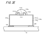
- FIG. 3E shows the LED chip 111 a and the base 111 b mounted on the printed circuit board 12.
- the LED chip 111a is mounted on the printed circuit board 12 via the base 111b, and emits light in a direction away from the printed circuit board 12.
- the LED chip 111a is located at the center of the base 111b when the light emitting device 11 is viewed in plan in the X direction.
- the light emission control by the LED chips 111 a can be controlled independently of each other. Thereby, the backlight unit 1 can perform partial dimming control (local dimming).
- solder is respectively applied to the two connection terminal portions 121 of the conductive layer pattern included in the printed circuit board 12, and the base is attached to the solder.
- the base 111b and the LED chip 111a fixed to the base 111b are placed on the printed circuit board 12 by, for example, an automatic machine (not shown) so that the two electrodes 111c provided on the bottom surface of the main body 111g match each other.
- the printed circuit board 12 on which the base 111b and the LED chip 111a fixed to the base 111b are placed is sent to a reflow bath that irradiates infrared rays, and the solder is heated to about 260 ° C., and the base 111b, the printed circuit board 12, Is soldered.
- the lens 112 is provided in contact with the LED chip 111a by insert molding so as to cover the base 111b that supports the LED chip 111a, and reflects or refracts light emitted from the LED chip 111a in a plurality of directions. That is, light is diffused.
- the lens 112 is a transparent lens, and is made of, for example, silicon resin or acrylic resin.
- the upper surface 112a which is the surface facing the liquid crystal panel 2, is curved with a recess in the center, and the side surface 112b is formed in a substantially cylindrical shape parallel to the optical axis S of the LED chip 111a.
- the diameter L2 in the cross section orthogonal to the base is, for example, 10 mm and is provided to extend outward with respect to the base 111b. That is, the lens 112 is larger than the base 111b in the direction orthogonal to the optical axis S of the LED chip 111a (the diameter L2 of the lens 112 is larger than the length L1 of one side of the support surface of the base 111b).
- the lens 112 is provided to extend outward with respect to the base 111b, so that the light emitted from the LED chip 111a can be diffused by the lens 112 over a wide range.
- the height H1 of the lens 112 is 4.5 mm, for example, and is smaller than the diameter L2.
- the lens 112 has a length (diameter L2) in a direction orthogonal to the optical axis S of the LED chip 111a larger than the height H1. The light incident on the lens 112 is diffused in the direction intersecting the optical axis S inside the lens 112.
- the reason why the diameter L2 is set to be larger than the height H1 is to make the backlight unit 1 thin and to uniformly irradiate the liquid crystal panel 2.
- uneven illuminance tends to occur on the back surface 22 of the liquid crystal panel 2, and as a result, uneven brightness tends to occur on the front surface 21 of the liquid crystal panel 2.
- the lens 112 By making the diameter L2 of the light source larger than the height H1, the backlight unit 1 can be made thinner and the liquid crystal panel 2 can be uniformly irradiated with light.
- the diameter L2 of the lens 112 is made smaller than the height H1 of the lens 112, not only thinning and uniform irradiation become difficult, but also in insert molding for molding the lens 112 in accordance with the LED chip 111a. There arises a problem that the balance tends to deteriorate. Further, when soldering the light emitting unit 111 composed of the LED chip 111a and the base 111b and the insert-molded lens 112 to the printed circuit board 12, the balance is easily lost, and there is a problem in assembly.
- the upper surface 112a of the lens 112 includes a central portion 1121, a first curved portion 1122, and a second curved portion 1123.
- the curved upper surface 112a having a dent in the central portion reflects the first light that is reflected and emitted from the side surface 112b, and the first light that is refracted outward is emitted from the upper surface 112a.
- a second region. The first region is formed in the first curved portion 1122, and the second region is formed in the second curved portion 1123.
- the central portion 1121 is formed at the central portion of the upper surface 112a facing the liquid crystal panel 2, and the center of the central portion 1121 (that is, the optical axis of the lens 112) is located on the optical axis S of the LED chip 111a.
- the central portion 1121 is formed in a circular shape parallel to the light emitting surface of the LED chip 111a, and its diameter L3 is, for example, 1 mm.
- the central portion 1121 has a circular bottom surface instead of the circular shape, and a conical side surface protruding from the bottom surface toward the LED chip 111a. You may make it a shape.
- the central portion 1121 is formed to irradiate light to a region facing the central portion 1121 in the diffusion plate 3 that is an irradiated body.
- the central portion 1121 is a portion facing the LED chip 111a, most of the light emitted from the LED chip 111a reaches the central portion 1121, and when most of the light is transmitted as it is, it faces the central portion 1121.
- the illuminance of the area to be markedly increased. Therefore, it is preferable that the shape of the central portion 1121 is the side shape of the cone. In the case of the conical side surface shape, most of the light is reflected by the central portion 1121 and less light is transmitted through the central portion 1121, so that the illuminance of the region facing the central portion 1121 can be suppressed.
- the first curved portion 1122 is connected to the outer peripheral edge of the central portion 1121 and extends outward in one of the directions of the optical axis S of the LED chip 111a (direction toward the liquid crystal panel 2). It is an annular curved surface that is curved so as to be convex in one direction. The shape of this curved surface is designed so that the light emitted from the LED chip 111a is totally reflected.
- the light that has reached the first curved portion 1122 is totally reflected by the first curved portion 1122, and then passes through the side surface 112b of the lens to the reflecting member 113. Head.
- the light that has reached the reflecting member 113 is diffused by the reflecting member 113, and is irradiated on a region that is not opposed to the LED chip 111a in the diffusing plate 3 that is an irradiated body. Thereby, the irradiation light quantity to the area
- the first curved portion 1122 is formed so that the incident angle of the light emitted from the LED chip 111a is greater than or equal to the critical angle ⁇ in order to totally reflect the light emitted from the LED chip 111a.
- the lens 112 is made of an acrylic resin
- the critical angle ⁇ is 42.1 °
- the first curved portion 1122 is formed in a shape with an incident angle of 42.1 ° or more.
- the second curved portion 1123 is connected to the outer peripheral edge of the first curved portion 1122, and extends outward in the optical axis S direction of the LED chip 111a (in a direction away from the liquid crystal panel 2). It is an annular curved surface that is curved so as to be convex in one direction in the optical axis S direction.
- the lens 112 is provided such that the bottom surface thereof abuts on a base portion 1131 of a reflection member 113 described later.
- the light that has reached the second curved portion 1123 is refracted in the direction toward the light emitting portion 111 when passing through the second curved portion 1123, and the diffusing plate 3 and the reflecting member. Head to 113.
- the light reaching the reflection member 113 is diffused and travels toward the diffusion plate 3.
- the light traveling toward the diffusion plate 3 by the second curved portion 1123 is mainly irradiated to a region different from the region irradiated with light by the central portion 1121 and the first curved portion 1122 in the diffusion plate 3.
- the amount of light is complemented. Since the second curved portion 1123 needs to transmit light, the incident angle is less than 42.1 ° so as not to totally reflect the light emitted from the LED chip 111a.
- the lens 112 is formed with the first curved portion 1122 that totally reflects the light emitted from the LED chip 111a toward the side surface 112b of the lens 112 at the outer peripheral edge portion of the central portion 1121.
- a second curved portion 1123 that refracts the light emitted from the LED chip 111a is formed at the outer peripheral edge of the curved portion 1122.
- the LED chip 111a generally has high directivity, the amount of light near the optical axis S is extremely large, and the amount of light decreases as the light emission angle with respect to the optical axis S increases.
- the first curved portion 1122 that totally reflects light toward the region is formed around the central portion 1121 through which the optical axis S passes. The amount of irradiation light can be increased.
- the second curved portion 1123 is formed adjacent to the periphery of the central portion 1121, and the first curved portion 1122 is formed adjacent to the second curved portion 1123,
- the emission angle of the light toward the first curved portion 1122 with respect to the optical axis S increases, and as a result, the amount of light that is totally reflected by the first curved portion 1122 and applied to the region is reduced.
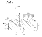
- FIG. 4 is a diagram for explaining the optical path of the light emitted from the LED chip 111a.
- Light emitted from the LED chip 111 a enters the lens 112 and is diffused by the lens 112. Specifically, of the light incident on the lens 112, the light that has reached the central portion 1121 on the upper surface 112a facing the liquid crystal panel 2 is emitted in the direction of the arrow A1 toward the liquid crystal panel 2, and the first curved portion.
- the light that has reached 1122 is totally reflected and emitted from the side surface 112b in the direction of the arrow A2, and the light that has reached the second curved portion 1123 is refracted outward (in a direction away from the LED chip 111a) and is refracted.
- the LED chip 111a and the lens 112 are such that the center of the lens 112 (that is, the optical axis of the lens 112) is positioned on the optical axis S of the LED chip 111a, and the lens 112 contacts the LED chip 111a. It is formed in advance so as to be in contact with each other with high accuracy.
- the LED chip 111a and the lens 112 can be pre-aligned and formed by insert molding, and the LED chip 111a supported by the base 111b is fitted into the lens 112 formed into a predetermined shape. The method of combining can be mentioned.
- the LED chip 111a and the lens 112 are formed by being previously aligned by insert molding.
- Molding is performed by injecting a resin, which is a raw material of the lens 112, from a resin inlet into a space formed when the upper surface mold and the lower surface mold are combined.
- the resin as the raw material of the lens 112 is injected from the resin injection port. You may make it shape
- the backlight unit 1 can accurately reflect and refract the light emitted from the LED chip 111a by the lens 112 in contact with the LED chip 111a, so that the distance from the diffusion plate 3 to the printed board 12 Even in the thin liquid crystal display device 100 with a small H3, the liquid crystal panel 2 can be irradiated with light so that the luminance of the liquid crystal panel 2 is uniform in the surface direction.
- the reflecting member 113 will be described with reference to FIGS.
- FIG. 5 is a perspective view of the reflecting member 113 and the lens 112
- FIG. 6 is a diagram when the reflecting member 113 and the lens 112 are viewed in plan in the X direction.
- the reflection member 113 is a member that reflects incident light toward the liquid crystal panel 2.
- the reflection member 113 has a polygonal outer shape when viewed in plan in the X direction, for example, a square shape.
- the reflection member 113 has a square flat plate-like base portion 1131 having an opening at the center and a length of one side of 38.8 mm, and surrounds the base portion 1131 so as to move away from the printed circuit board 12 as the distance from the LED chip 111a increases.
- the reflecting member 113 constituted by the base portion 1131 and the inclined portion 1132 is provided in an inverted dome shape centering on the LED chip 111a (not shown in FIGS. 5 and 6) provided in the lens 112.
- the reflecting member 113 has a square outer shape when seen in a plan view in the X direction, and is configured to be symmetrical with respect to the square diagonal line. Further, the center point of the square shape is configured to be 90 ° rotationally symmetric.
- the base 1131 is formed so that each square side when viewed in plan in the X direction is parallel to the row direction or the column direction of the plurality of LED chips 111a arranged in a matrix.
- the base 1131 is formed along the printed circuit board 12 and has a square opening at the center when viewed in plan in the X direction.
- the length of one side of the square opening is approximately the same as the length L1 of one side of the base 111b that supports the LED chip 111a, and the base 111b is inserted through this opening.
- the inclined portion 1132 is a generic name for four trapezoidal flat plates 1132a having a trapezoidal main surface.
- the shorter base 1132aa of the trapezoid is connected to each side of the base 1131 having a square shape, and the longer base 1132ab is separated from the printed circuit board 12 more than the base 1131 in the X direction.
- the adjacent trapezoidal flat plates 1132a are connected to each other on the side 1132ac.
- the inclination angle ⁇ 1 between the trapezoidal flat plate 1132a and the printed board 12 shown in FIG. 2A is, for example, 80 °. Further, the height H2 of the inclined portion 1132 in the X direction is, for example, 3.5 mm.
- the base portion 1131 and the inclined portion 1132 are made of highly bright PET (Polyethylene Terephthalate) and aluminum.
- High-brightness PET is foamable PET containing a fluorescent agent, and examples thereof include E60V (trade name) manufactured by Toray Industries, Inc.
- the thickness of the base portion 1131 and the inclined portion 1132 is, for example, 0.1 to 0.5 mm.
- a region that becomes a corner of the square reflection member 113 in the inclined portion 1132 is referred to as a corner portion 113 b.
- a region that is a side of the square-shaped reflecting member 113 in the inclined portion 1132 and that excludes the corner portion 113b is referred to as a side portion 113a.
- a region overlapping the lens 112 in the base portion 1131 when viewed in plan in the X direction is referred to as a central portion 113c.
- first reflection region 113d a region between the corner portion 113b and the central portion 113c in the base portion 1131 is referred to as a first reflection region 113d.
- the width L4 of the first reflective region 113d is 10 mm to 25 mm.
- second reflection region 113e a region between the side portion 113a and the central portion 113c in the base portion 1131 is referred to as a second reflection region 113e.
- the width L5 of the second reflection region 113e is 15 mm to 35 mm.
- the first reference reflecting portion 113f is a portion where the total reflectance with respect to visible light emitted from the LED chip 111a is a predetermined value, for example, 90% to 99% in the first reflecting region 113d.
- the high reflection portion 113g is a portion having a total reflectance higher than that of the first reference reflection portion 113f in the first reflection region 113d.
- the highly reflective portion 113g is formed by sticking a highly bright PET sheet on the base portion 1131.
- the reflective member 113 having the high reflection portion 113g may be formed by molding a high-brightness PET or the like using a mold having a mirror finish on a part thereof. In this case, a part of the base portion 1131 becomes the high reflection portion 113g.
- the total reflectance of the high reflection portion 113g is 97%.
- the total reflectance of the first reference reflecting portion 113f is 94%.
- the total reflectance of the second reflection region 113e, the side portions 113a, the corner portions 113b, and the central portion 113c is also 94%.
- the total reflectance is the sum of the specular reflectance and the diffuse reflectance as defined in JIS H 0201: 1998, and can be measured according to JIS K 7375.
- the diffuse reflection range of the high reflection portion 113g is narrower than the diffuse reflection range of the second reflection region 113e.
- the diffuse reflection range is a numerical value indicating the degree of light spreading when diffuse reflection occurs on a certain surface. More specifically, when light of a predetermined spot diameter is incident on a certain surface at a predetermined incident angle so as to have a predetermined illuminance, it is sufficiently larger than the spot diameter from the centroid position of that surface. It is provided at a certain distance, and at every position where illuminance exceeding a predetermined illuminance threshold is detected by a detector having a detection surface having an area sufficiently smaller than the area of a virtual spherical surface having a radius of the certain distance.
- the diffuse reflection range of the high reflection portion 113g is, for example, 1/3 to 1/8 times the diffuse reflection range of the second reflection region 113e.
- the diffuse reflection ranges of the first reference reflection portion 113f, the side portions 113a, the corner portions 113b, and the central portion 113c are equal to the diffuse reflection range of the second reflection region 113e.
- one high reflection portion 113g is provided in one first reflection region 113d.
- the high reflection portion 113g is formed in a square shape at the central portion of the first reflection region 113d, and the length of one side of the square shape is, for example, 5 mm.
- the region other than the high reflection portion 113g is the first reference reflection portion 113f. Note that the number, shape, and size of the high reflection portions 113g are not limited to those described above.
- FIG. 7 shows a modification of the first embodiment.
- one isosceles triangular high reflection portion 113g is formed in each of the first reflection regions 113d at a portion surrounded by the corner portion 113b.
- the length of the hypotenuse of the isosceles triangle-shaped highly reflective portion 113g is, for example, 8 mm.
- the reflection members 113 configured as described above and provided in each of the plurality of light emitting devices 11 are integrally formed with each other.
- an extrusion molding process can be cited.
- the reflecting member 113 is made of aluminum, A press working can be mentioned.
- integrally forming the reflection members 113 respectively provided in the plurality of light emitting units 111 the accuracy of the arrangement positions of the plurality of light emitting units 111 with respect to the printed circuit board 12 can be improved, and Since the number of operations for attaching the reflecting member 113 can be reduced during the assembly operation, the efficiency of the assembly operation can be improved.
- FIG. 8 is a perspective view of the light emitting unit 111 and the reflecting member 113 shown in FIG. 6, and the lens 112 is omitted.
- the light reaching the central portion 1121 on the upper surface 112 a facing the liquid crystal panel 2 is directed toward the liquid crystal panel 2.
- the light that is emitted in the direction of the arrow A1 and reaches the first curved portion 1122 is reflected and emitted from the side surface 112b in the direction of the arrow A2 and the light that reaches the second curved portion 1123 is refracted outward. Then, it is emitted toward the liquid crystal panel 2 in the direction of the arrow A3.
- Part of the light traveling from the central portion 113c of the reflecting member 113 toward the corner portion 113b in the plane direction orthogonal to the X direction travels as shown in the optical path A4 in FIG. 8, and is mirrored by the high reflecting portion 113g of the first reflecting region 113d. Reflected and diffusely reflected to reach the corner 113b. When the light reaches the corner 113b, specular reflection and diffuse reflection occur at the corner 113b, and the light reaches the portion facing the corner 113b in the liquid crystal panel 2.
- part of the light traveling from the central portion 113c of the reflecting member 113 to the side portion 113a in the plane direction orthogonal to the X direction travels as in the optical path A5 shown in FIG. 8, and is specularly reflected and diffused by the second reflecting region 113e. It is reflected and reaches the side 113a.
- specular reflection and diffuse reflection occur at the side 113a, and reaches the portion of the liquid crystal panel 2 that faces the side 113a.
- the reflection member 113 includes a high reflection portion 113g having a total reflectance higher than that of the first reference reflection portion 113f, the side portions 113a, the corner portions 113b, and the second reflection region 113e in the first reflection region 113d. Therefore, the average total reflectance at the corner portion 113b and the first reflection region 113d is higher than the average total reflectance at the side portion 113a and the second reflection region 113e.
- the average total reflectivity is an average value of the total reflectivity, with the total reflectivity weighted by the area of the surface having the reflectivity.
- the average total reflectivity at the corner portion 113b and the first reflection region 113d is higher than the average total reflectivity at the side portion 113a of the reflection member 113 and the second reflection region 113e.
- the ratio of the amount of light that is reflected by the first reflecting region 113d and the corner 113b and reaches the liquid crystal panel 2 to the amount of light that is reflected by the reflecting region 113e and the side portion 113a and reaches the liquid crystal panel 2 is conventionally higher than the ratio. Will also increase. That is, the ratio of the amount of light reaching the portion facing the corner 113b in the liquid crystal panel 2 to the amount of light reaching the portion facing the side 113a in the liquid crystal panel 2 is increased as compared with the conventional case.
- the backlight unit 1 can make the light irradiated to the liquid crystal panel 2 uniform, and the liquid crystal display device 100 provided with the backlight unit 1 can display a higher quality image.
- the diffuse reflection range of the high reflection portion 113g is narrower than the diffuse reflection range of the second reflection region 113e. That is, the light reflected by the high reflection portion 113g diffuses in a narrower range than the light reflected by the second reflection region 113e. Accordingly, the ratio of the amount of light reaching the portion facing the corner 113b of the reflecting member 113 in the liquid crystal panel 2 to the amount of light reaching the portion facing the side 113a of the reflecting member 113 in the liquid crystal panel 2 is conventionally determined.
- the backlight unit 1 can make the light applied to the liquid crystal panel 2 more uniform.
- the reflecting member 113 includes a base portion 1131 and an inclined portion 1132. Since the inclined portion 1132 is inclined so as to approach the liquid crystal panel 2 as the distance from the LED chip 111a increases, the light emitted from the LED chip 111a is exposed to the side 113a of the reflecting member 113 in the liquid crystal panel 2 and the corners. It is easy to reach the part facing the portion 113b. Therefore, the backlight unit 1 can make the light applied to the liquid crystal panel 2 more uniform.
- FIG. 9 is a diagram when the reflecting member 120 and the lens 112 are viewed in plan in the X direction.
- the reflection member 120 includes a side part 120a, a corner part 120b, a center part 120c, a first reflection area 120d, and a second reflection area 120e when viewed in plan in the X direction.
- the side part 120a, the corner part 120b, the central part 120c, the first reflection area 120d, and the second reflection area 120e are respectively the side part 113a, the corner part 113b, the central part 113c, and the first reflection area in the first embodiment. 113d and the second reflection region 113e.
- the second reference area 120e is provided with a second reference reflection part 120f and a first low reflection part 120g.
- the second reference reflecting portion 120f is a portion where the total reflectance with respect to visible light emitted from the LED chip 111a is a predetermined value, for example, 90% to 99% in the second reflecting region 120e.
- the first low reflection portion 120g is a portion where the total reflectance in the second reflection region 120e is lower than the total reflectance of the second reference reflection portion 120f.
- the first low reflection portion 120g is formed by coloring a part of the reflection member 120 with a black or gray colorant. Note that the surface of the colored portion may be roughened by sandblasting or the like.
- the total reflectance of the first low reflection portion 120g is, for example, 40% to 80%, and 75% in the present embodiment.
- the total reflectance of the second reference reflecting portion 120f is 94%.
- the total reflectance of the first reflection region 120d, the side portions 120a, the corner portions 120b, and the central portion 120c is also 94%.
- the diffuse reflection range of the first low reflection portion 120g is wider than the diffuse reflection range of the first reflection region 120d.
- the diffuse reflection range of the first low reflection portion 120g is, for example, 1.2 to 5 times the diffuse reflection range of the first reflection region 120d.
- the diffuse reflection range of the second reference reflection portion 120f, the side portion 120a, the corner portion 120b, and the central portion 120c is equal to the diffuse reflection range of the first reflection region 120d.
- one first low reflection portion 120g is provided in one second reflection region 120e.
- the first low reflection part 120g is formed in a rectangular shape extending from the central part 120c of the reflection member 120 toward the side part 120a in the central part of the second reflection region 120e, and the length of the long side of the rectangular shape is For example, it is 15 mm, and the length of the short side is, for example, 3 mm.
- the region other than the first low reflection portion 120g is a second reference reflection portion 120f. Note that the number, shape, and size of the first low reflection portions 120g are not limited to those described above.
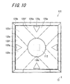
- FIG. 10 shows a modification of the second embodiment.
- the regular triangular first low reflection portions 120g are formed one by one so as to protrude in the direction from the side portion 120a to the central portion 120c in each second reflection region 120e. Yes.
- the length of one side of the regular low triangular first low reflection portion 120g is, for example, 3 mm.
- the light emitted from the LED chip 111a is reflected by the reflection member 120 and applied to the liquid crystal panel 2.
- the reflection member 120 includes a first low reflection portion having a total reflectance lower than that of the second reference reflection portion 120f, the side portion 120a, the corner portion 120b, and the first reflection region 120d in the second reflection region 120e. Since it has 120 g, the average total reflectance in the corner portion 120b and the first reflection region 120d is higher than the average total reflectance in the side portion 120a and the second reflection region 120e.
- the average total reflectivity at the corner portion 120b and the first reflection region 120d is higher than the average total reflectivity at the side portion 120a of the reflection member 120 and the second reflection region 120e.
- the ratio of the amount of light that is reflected by the first reflection region 120d and the corner portion 120b and reaches the liquid crystal panel 2 to the amount of light that is reflected by the reflection region 120e and the side portion 120a and reaches the liquid crystal panel 2 has been Will also increase. That is, the ratio of the amount of light reaching the portion facing the corner portion 120b in the liquid crystal panel 2 to the amount of light reaching the portion facing the side portion 120a in the liquid crystal panel 2 is increased as compared with the conventional case.
- the backlight unit 1 can make the light irradiated to the liquid crystal panel 2 uniform, and the liquid crystal display device 100 provided with the backlight unit 1 can display a higher quality image.
- the diffuse reflection range of the first low reflection portion 120g is wider than the diffuse reflection range of the first reflection region 120d. That is, the light reflected by the first low reflection part 120g is diffused in a wider range than the light reflected by the first reflection region 120d. Accordingly, the ratio of the amount of light reaching the portion facing the corner portion 120b of the reflective member 120 in the liquid crystal panel 2 to the amount of light reaching the portion facing the side portion 120a of the reflective member 120 in the liquid crystal panel 2 is conventionally determined.
- the backlight unit 1 can make the light applied to the liquid crystal panel 2 more uniform.
- FIG. 11 is a diagram when the reflecting member 130 and the lens 112 are viewed in plan in the X direction.
- the reflection member 130 includes a side portion 130a, a corner portion 130b, a central portion 130c, a first reflection region 130d, and a second reflection region 130e when viewed in plan in the X direction.
- the side part 130a, the corner part 130b, the central part 130c, the first reflection area 130d, and the second reflection area 130e are respectively the side part 113a, the corner part 113b, the central part 113c, and the first reflection area in the first embodiment. 113d and the second reflection region 113e.
- the side portion 130a is provided with a third reference reflection portion 130f and a second low reflection portion 130g.
- the third reference reflecting portion 130f is a portion where the total reflectance with respect to visible light emitted from the LED chip 111a is a predetermined value, for example, 90% to 99% in the side portion 130a.
- the second low reflection portion 130g is a portion where the total reflectance in the side portion 130a is lower than the total reflectance of the third reference reflection portion 130f.
- the second low reflection portion 130g is formed by coloring a part of the reflection member 130 with a black or gray colorant. Note that the surface of the colored portion may be roughened by sandblasting or the like.
- the total reflectance of the second low reflection portion 130g is, for example, 40% to 80%, and 75% in this embodiment. Further, the total reflectance of the third reference reflecting portion 130f is 94%. Furthermore, the total reflectance of the first reflection region 130d, the second reflection region 130e, the corner portion 130b, and the central portion 130c is also 94%.
- the diffuse reflection range of the second low reflection portion 130g is wider than the diffuse reflection range of the first reflection region 130d.
- the diffuse reflection range of the second low reflection portion 130g is, for example, 2 to 8 times the diffuse reflection range of the first reflection region 130d.
- the diffuse reflection range of the third reference reflective portion 130f, the second reflective region 130e, the corner portion 130b, and the central portion 130c is equal to the diffuse reflective range of the first reflective region 130d.
- one second low reflection portion 130g is provided in one side portion 130a.
- the second low reflection portion 130g is formed in a rectangular shape extending along the longitudinal direction of the side portion 130a at the center portion of the side portion 130a, and the length of the long side of the rectangular shape is, for example, 8 mm.
- the length of the short side is 1.5 mm, for example.
- a region other than the second low reflection portion 130g is a third reference reflection portion 130f. Note that the number, shape, and size of the second low reflection portions 130g are not limited to those described above.
- the light emitted from the LED chip 111a is reflected by the reflection member 130 and applied to the liquid crystal panel 2.
- the reflection member 130 has a second low reflection portion having a total reflectance lower than that of the third reference reflection portion 130f, the corner portion 130b, the first reflection region 130d, and the second reflection region 130e on the side portion 130a. Since it has 130 g, the average total reflectance in the corner portion 130 b and the first reflection region 130 d is higher than the average total reflectance in the side portion 130 a and the second reflection region 130 e.
- the average total reflectance at the corner portion 130b and the first reflection region 130d is higher than the average total reflectance at the side portion 130a and the second reflection region 130e of the reflection member 130.
- the ratio of the amount of light reflected by the first reflective region 130d and the corner portion 130b and reaching the liquid crystal panel 2 to the amount of light reflected by the reflective region 130e and the side portion 130a and reaching the liquid crystal panel 2 has been conventionally increased. Will also increase. That is, the ratio of the amount of light reaching the portion facing the corner portion 130b in the liquid crystal panel 2 to the amount of light reaching the portion facing the side portion 130a in the liquid crystal panel 2 is increased as compared with the conventional case.
- the backlight unit 1 can make the light irradiated to the liquid crystal panel 2 uniform, and the liquid crystal display device 100 provided with the backlight unit 1 can display a higher quality image.
- the diffuse reflection range of the second low reflection portion 130g is wider than the diffuse reflection range of the first reflection region 130d. That is, the light reflected by the second low reflection part 130g is diffused in a wider range than the light reflected by the first reflection region 130d. Accordingly, the ratio of the amount of light reaching the portion facing the corner portion 130b of the reflecting member 130 in the liquid crystal panel 2 to the amount of light reaching the portion facing the side portion 130a of the reflecting member 130 in the liquid crystal panel 2 is conventionally determined.
- the backlight unit 1 can make the light applied to the liquid crystal panel 2 more uniform.
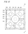
- FIG. 12 is a diagram when the reflecting member 140 and the lens 112 are viewed in plan in the X direction.
- the reflection member 140 includes a side portion 140a, a corner portion 140b, a center portion 140c, a first reflection region 140d, and a second reflection region 140e when viewed in plan in the X direction.
- the side part 140a, the corner part 140b, the central part 140c, the first reflection area 140d, and the second reflection area 140e are respectively the side part 113a, the corner part 113b, the central part 113c, and the first reflection area in the first embodiment. 113d and the second reflection region 113e.
- the first reference reflecting portion 140f is a portion where the total reflectance with respect to visible light emitted from the LED chip 111a is a predetermined value, for example, 90% to 99% in the first reflecting region 140d.
- the high reflection portion 140g is a portion having a total reflectance higher than that of the first reference reflection portion 140f in the first reflection region 140d.
- the high reflection part 140g is formed by sticking a high-brightness PET sheet on the reflection member 140.
- the reflecting member 140 having the high reflection portion 140g may be formed by molding a high-brightness PET or the like using a mold having a mirror-finished part.
- the second reference area 140e is provided with a second reference reflection part 140h and a first low reflection part 140i.
- the second reference reflection part 140h is a part in which the total reflectance is equal to the total reflectance of the first reference reflection part 140f in the second reflection region 140e.
- the first low reflection portion 140i is a portion where the total reflectance in the second reflection region 140e is lower than the total reflectance of the second reference reflection portion 140h.
- the first low reflection portion 140i is formed by coloring a part of the reflection member 140 with a black or gray colorant. Note that the surface of the colored portion may be roughened by sandblasting or the like.
- the total reflectance of the high reflection portion 140g is 97%.
- the total reflectance of the first low reflection portion 140i is, for example, 40% to 80%, and is 75% in the present embodiment.
- the total reflectance of the first reference reflection part 140f, the second reference reflection part 140h, the side part 140a, the corner part 140b, and the center part 140c is 94%.
- the diffuse reflection range of the high reflection portion 140g is narrower than the diffuse reflection range of the second reference reflection portion 140h of the second reflection region 140e.
- the diffuse reflection range of the high reflection portion 140g is, for example, 1/3 to 1/8 times the diffuse reflection range of the second reference reflection portion 140h.
- the diffuse reflection range of the first low reflection portion 140i is wider than the diffuse reflection range of the first reference reflection portion 140f of the first reflection region 140d.
- the diffuse reflection range of the first low reflection portion 140i is, for example, the diffuse reflection range of the first reference reflection portion 140f. 1.2 times to 5 times.
- the diffuse reflection ranges of the first reference reflection part 140f, the second reference reflection part 120h, the side part 120a, the corner part 120b, and the center part 120c are equal to each other.
- one high reflection portion 140g is provided in one first reflection region 140d.
- the high reflection portion 140g is formed in a square shape at the central portion of the first reflection region 140d, and the length of one side of the square shape is, for example, 5 mm.
- the region other than the high reflection portion 140g is a first reference reflection portion 140f. Note that the number, shape, and size of the high reflection portions 140g are not limited to those described above.
- one first low reflection portion 140i is provided in one second reflection region 140e.
- the first low reflection portion 140i is formed in a rectangular shape at the center of the second reflection region 140e, and the length of the long side of the rectangular shape is, for example, 15 mm, and the length of the short side is, for example, 2 mm.
- the region other than the first low reflection portion 140i is the second reference reflection portion 140h. Note that the number, shape, and size of the first low reflection portions 140i are not limited to those described above.
- the light emitted from the LED chip 111a is reflected by the reflection member 140 and applied to the liquid crystal panel 2.
- the reflection member 140 has a total reflection higher than the total reflection rate of the first reference reflection part 140f, the side part 140a, the corner part 140b, the second reference reflection part 140h, and the first low reflection part 140i in the first reflection region 140d.
- High reflection part 140g having a refractive index, and total reflection of second reference reflection part 140h, side part 140a, corner part 140b, first reference reflection part 140f, and high reflection part 140g in second reflection region 140e.
- a first low reflection portion 140i having a total reflectance lower than the first reflectance. Therefore, the average total reflectivity at the corner portion 140b and the first reflection region 140d is higher than the average total reflectivity at the side portion 140a and the second reflection region 140e.
- the average total reflectance in the corner portion 140b and the first reflection region 140d is higher than the average total reflectance in the side portion 140a and the second reflection region 140e of the reflection member 140.
- the ratio of the amount of light that is reflected by the first reflection region 140d and the corner portion 140b and reaches the liquid crystal panel 2 to the amount of light that is reflected by the reflection region 140e and the side portion 140a and reaches the liquid crystal panel 2 is conventionally higher than that of FIG. Will also increase. That is, the ratio of the amount of light reaching the portion facing the corner portion 140b in the liquid crystal panel 2 to the amount of light reaching the portion facing the side portion 140a in the liquid crystal panel 2 is increased as compared with the conventional case.
- the backlight unit 1 can make the light irradiated to the liquid crystal panel 2 uniform, and the liquid crystal display device 100 provided with the backlight unit 1 can display a higher quality image.
- the diffuse reflection range of the high reflection portion 140g is narrower than the diffuse reflection range of the second reflection region 140e, and the diffuse reflection range of the first low reflection portion 140i is equal to that of the first reflection region 140d. It is wider than the diffuse reflection range. That is, the light reflected by the high reflection portion 140g diffuses in a narrower range than the light reflected by the second reflection region 140e, and the light reflected by the first low reflection portion 140i is reflected by the second reflection region 140e. Diffuses over a wider area than the reflected light.
- the ratio of the amount of light reaching the portion facing the corner portion 140b of the reflecting member 140 in the liquid crystal panel 2 to the amount of light reaching the portion facing the side portion 140a of the reflecting member 140 in the liquid crystal panel 2 is conventionally determined.
- the backlight unit 1 can make the light applied to the liquid crystal panel 2 more uniform.
- Liquid crystal panel 100 Liquid crystal display device 111a LED chip 111b Base 112 Lens 113,120,130,140 Reflective member 113a, 120a, 130a, 140a Side part 113b, 120b, 130b, 140b Corner
Landscapes
- Physics & Mathematics (AREA)
- Nonlinear Science (AREA)
- General Engineering & Computer Science (AREA)
- Engineering & Computer Science (AREA)
- Optics & Photonics (AREA)
- General Physics & Mathematics (AREA)
- Crystallography & Structural Chemistry (AREA)
- Chemical & Material Sciences (AREA)
- Mathematical Physics (AREA)
- Planar Illumination Modules (AREA)
- Liquid Crystal (AREA)
- Fastening Of Light Sources Or Lamp Holders (AREA)
- Non-Portable Lighting Devices Or Systems Thereof (AREA)
- Led Device Packages (AREA)
Abstract
本発明は、表示パネルを備える表示装置のバックライトユニットに用いられる発光装置において、表示パネルの輝度がその表示パネルの面方向において均一となるように、光を表示パネルに照射することができ、薄型化が可能な発光装置、および、この発光装置を備える表示装置に関する。バックライトユニット(1)に、プリント基板(12)と、基台(111b)、LEDチップ(111a)、およびレンズ(112)を有する複数の発光部(111)と、発光部(111)を取り囲む反射部材(113)とを設け、反射部材(113)の第1反射領域(113d)に高反射部(113g)を形成する。
Description
本発明は、表示パネルの背面に光を照射するバックライトユニットに設けられる発光装置、この発光装置を備える表示装置に関する。
表示パネルは、2枚の透明基板の間に液晶が封入され、電圧が印加されることにより液晶分子の向きが変えられ光透過率を変化させることで予め定められた映像等が光学的に表示される。この表示パネルには、液晶自体が発光体ではないので、たとえば透過型の表示パネルの背面側に冷陰極管(CCFL)、発光ダイオード(LED:Light Emitting Diode)などを光源とした光を照射するバックライトユニットが備えられる。
バックライトユニットには、冷陰極管やLED等の光源を底面に並べて光を出す直下型と、冷陰極管やLED等の光源を導光板と呼ばれる透明な板のエッジ部に配して、導光板エッジから光を通して背面に設けられたドット印刷やパターン形状によって前面に光を出すエッジライト型とがある。
LEDは、低消費電力、長寿命、水銀を使わないことによる環境負荷低減などの優れた特性を有するが、価格的に高価であることと、青色発光LEDが発明されるまでは白色発光LEDは無かったことと、さらに強い指向性を有していることとから、バックライトユニットの光源としての利用が遅れていた。しかしながら近年、照明用途で、高演色高輝度白色LEDが急速に普及しており、それに伴ってLEDが安価になってきているので、バックライトユニットの光源としては、冷陰極管からLEDへの移行が進んでいる。
LEDは強い指向性を有するので、表示パネルの背面において面方向に輝度を均一化して光を照射するという観点では、直下型よりもエッジライト型が有効である。しかしながら、エッジライト型のバックライトユニットは、導光板のエッジ部に集中して光源が配置されることにより光源によって生じた熱が集中するという問題とともに、表示パネルのベゼル部が大きくなるという問題が生じる。さらに、エッジライト型のバックライトユニットは、表示画像の高品質化および省電力化が可能な制御方法として注目されている部分的な調光制御(ローカルディミング)についても制約が大きく、表示画像の高品質化および省電力化が達成可能な小分割領域の制御ができないという問題がある。
そこで、部分的な調光制御に有利な直下型のバックライトユニットにおいて、強い指向性を有するLEDを光源として用いた場合であっても、被照射体の輝度がその被照射体の面方向において均一となるように、光を表示パネルに照射することが可能な方法の検討が進められている。
たとえば、特許文献1には、発光素子と、その発光素子を覆うように設けられた逆円錐形状の窪みを有する樹脂レンズと、樹脂レンズの周囲に設けられた反射板とを備える逆円錐型発光素子ランプが開示されている。また、特許文献2には、発光素子と、発光素子から出射された光を光軸と直交する方向に反射させながら導光する導光反射体とを備える光源ユニットが開示されている。
特許文献1および2に開示される技術では、発光素子から出射された強い指向性を有する光を、発光素子の光軸と交差する方向に拡散させ、面方向において光を表示パネルに照射することができる。
近年、表示装置の薄型化に対する要求が高まってきており、このような薄型化された表示装置に備えられる直下型の発光装置においては、発光素子から出射された光を発光素子の光軸と交差する方向に精度よく拡散させることが求められる。しかしながら、特許文献1および2に開示される技術では、上記の要求を充分に満足することはできない。
たとえば、特許文献2に開示される技術では、発光素子が反射板の底部の中心に設けられ、反射板の外形状は四角形状であり、反射板の側壁は、反射板の底部に対して垂直に設けられている。このように反射板の外形状が多角形状であると、発光素子から多角形状の角部までの距離は、辺部までの距離よりも長くなり、その結果、表示パネルにおいて角部に臨む部分に照射される光量は、辺部に臨む部分に照射される光量よりも少なくなり、表示パネルへの照射光量が不均一になってしまう。
本発明の目的は、表示パネルを備える表示装置のバックライトユニットに用いられる発光装置において、表示パネルの輝度がその表示パネルの面方向において均一となるように、光を表示パネルに照射することができ、薄型化が可能な発光装置、および、この発光装置を備える表示装置を提供することである。
本発明は、被照射体を照射する発光装置であって、
被照射体に光を照射する発光部と、
前記発光部の周囲に設けられる反射部材と、を備え、
前記反射部材は、
前記被照射体側から平面視したときの外形状が多角形状であり、
前記被照射体側から平面視したときにおける、前記反射部材の角部と前記角部および前記発光部の間の領域である第1反射領域とにおける平均的な全反射率が、前記反射部材の辺部と前記辺部および前記発光部の間の領域である第2反射領域とにおける平均的な全反射率よりも大きく、
前記発光部は、前記被照射体側から平面視したときに、前記反射部材の中央部に配置されることを特徴とする発光装置である。
被照射体に光を照射する発光部と、
前記発光部の周囲に設けられる反射部材と、を備え、
前記反射部材は、
前記被照射体側から平面視したときの外形状が多角形状であり、
前記被照射体側から平面視したときにおける、前記反射部材の角部と前記角部および前記発光部の間の領域である第1反射領域とにおける平均的な全反射率が、前記反射部材の辺部と前記辺部および前記発光部の間の領域である第2反射領域とにおける平均的な全反射率よりも大きく、
前記発光部は、前記被照射体側から平面視したときに、前記反射部材の中央部に配置されることを特徴とする発光装置である。
また本発明において、前記反射部材は、
前記第1反射領域内に、所定の全反射率を有する第1基準反射部と、前記所定の全反射率よりも高い全反射率を有する高反射部と、を有し、
前記角部、前記辺部、および前記第2反射領域の全反射率は、前記所定の全反射率に等しいことが好ましい。
前記第1反射領域内に、所定の全反射率を有する第1基準反射部と、前記所定の全反射率よりも高い全反射率を有する高反射部と、を有し、
前記角部、前記辺部、および前記第2反射領域の全反射率は、前記所定の全反射率に等しいことが好ましい。
また本発明において、前記反射部材は、
前記第2反射領域内に、所定の全反射率を有する第2基準反射部と、前記所定の全反射率よりも低い全反射率を有する第1低反射部と、を有し、
前記角部、前記辺部、および前記第1反射領域の全反射率は、前記所定の全反射率に等しいことが好ましい。
前記第2反射領域内に、所定の全反射率を有する第2基準反射部と、前記所定の全反射率よりも低い全反射率を有する第1低反射部と、を有し、
前記角部、前記辺部、および前記第1反射領域の全反射率は、前記所定の全反射率に等しいことが好ましい。
また本発明において、前記反射部材は、
前記辺部内に、所定の全反射率を有する第3基準反射部と、前記所定の全反射率よりも低い全反射率を有する第2低反射部と、を有し、
前記角部、前記第1反射領域、および前記第2反射領域の全反射率は、前記所定の全反射率に等しいことが好ましい。
前記辺部内に、所定の全反射率を有する第3基準反射部と、前記所定の全反射率よりも低い全反射率を有する第2低反射部と、を有し、
前記角部、前記第1反射領域、および前記第2反射領域の全反射率は、前記所定の全反射率に等しいことが好ましい。
また本発明において、前記反射部材は、
前記第1反射領域内に、所定の全反射率を有する第1基準反射部と、前記所定の全反射率よりも高い全反射率を有する高反射部と、を有し、
前記第2反射領域内に、前記所定の全反射率を有する第2基準反射部と、前記所定の全反射率よりも低い全反射率を有する第1低反射部と、を有し、
前記角部および前記辺部の全反射率は、前記所定の全反射率に等しいことが好ましい。
前記第1反射領域内に、所定の全反射率を有する第1基準反射部と、前記所定の全反射率よりも高い全反射率を有する高反射部と、を有し、
前記第2反射領域内に、前記所定の全反射率を有する第2基準反射部と、前記所定の全反射率よりも低い全反射率を有する第1低反射部と、を有し、
前記角部および前記辺部の全反射率は、前記所定の全反射率に等しいことが好ましい。
また本発明において、前記高反射部の拡散反射範囲は、前記第2反射領域の拡散反射範囲よりも狭いことが好ましい。
また本発明において、前記第1低反射部の拡散反射範囲は、前記第1反射領域の拡散反射範囲よりも広いことが好ましい。
また本発明において、前記第2低反射部の拡散反射範囲は、前記第1反射領域の拡散反射範囲よりも広いことが好ましい。
また本発明において、前記高反射部の拡散反射範囲は、前記第1基準反射部の拡散反射範囲よりも狭く、
前記第1低反射部の拡散反射範囲は、前記第1基準反射部の拡散反射範囲よりも広く、
前記第2基準反射部の拡散反射範囲は、前記第1基準反射部の拡散反射範囲に等しいことが好ましい。
前記第1低反射部の拡散反射範囲は、前記第1基準反射部の拡散反射範囲よりも広く、
前記第2基準反射部の拡散反射範囲は、前記第1基準反射部の拡散反射範囲に等しいことが好ましい。
また本発明において、前記反射部材は、前記発光素子を取り囲む基部と、前記基部を取り囲み、前記発光素子から離れるにつれて前記被照射体に近づくように傾斜する傾斜部と、を有することが好ましい。
また本発明は、表示パネルと、
前記表示パネルの背面に光を照射する前記発光装置を含む照明装置とを備えることを特徴とする表示装置である。
前記表示パネルの背面に光を照射する前記発光装置を含む照明装置とを備えることを特徴とする表示装置である。
本発明によれば、反射部材は、辺部と第2反射領域とにおける平均的な全反射率よりも、角部と第1反射領域とにおける平均的な全反射率の方が大きいので、第2反射領域および辺部で反射されて被照射体に到達する光の量に対する、第1反射領域および角部で反射されて被照射体に到達する光の量の比が、従来よりも増加する。すなわち、被照射体において反射部材の辺部に臨む部分に到達する光の量に対する、被照射体において反射部材の角部に臨む部分に到達する光の量の比が、従来よりも増加する。その結果、被照射体に照射される光を均一化することができる。
本発明によれば、第1反射領域に形成され、第1基準反射部、角部、辺部、および第2反射領域の全反射率よりも高い全反射率を有する高反射部により、被照射体において反射部材の角部に臨む部分に到達する光の量を増やすことができる。したがって、被照射体において反射部材の辺部に臨む部分に到達する光の量に対する、被照射体において反射部材の角部に臨む部分に到達する光の量の比を、従来よりも増加させることができ、被照射体に照射される光を均一化することができる。
本発明によれば、第2反射領域に形成され、第2基準反射部、角部、辺部、および第1反射領域の全反射率よりも低い全反射率を有する第1低反射部により、被照射体において反射部材の辺部に臨む部分に到達する光の量を減らすことができる。したがって、被照射体において反射部材の辺部に臨む部分に到達する光の量に対する、被照射体において反射部材の角部に臨む部分に到達する光の量の比を、従来よりも増加させることができ、被照射体に照射される光を均一化することができる。
本発明によれば、反射部材の辺部に形成され、第3基準反射部、角部、第1反射領域、および第2反射領域の全反射率よりも低い全反射率を有する第2低反射部により、被照射体において反射部材の辺部に臨む部分に到達する光の量を減らすことができる。したがって、被照射体において反射部材の辺部に臨む部分に到達する光の量に対する、被照射体において反射部材の角部に臨む部分に到達する光の量の比を、従来よりも増加させることができ、被照射体に照射される光を均一化することができる。
本発明によれば、第1反射領域に形成され、第1基準反射部、角部、辺部、および第2反射領域の全反射率よりも高い全反射率を有する高反射部により、被照射体において反射部材の角部に臨む部分に到達する光の量を増やすことができるとともに、反射部材の第2反射領域に形成され、第1基準反射部、第2基準反射部、高反射部、角部、および辺部の全反射率よりも低い全反射率を有する第1低反射部により、被照射体において反射部材の辺部に臨む部分に到達する光の量を減らすことができる。したがって、被照射体において反射部材の辺部に臨む部分に到達する光の量に対する、被照射体において反射部材の角部に臨む部分に到達する光の量の比を、従来よりも増加させることができ、被照射体に照射される光を均一化することができる。
本発明によれば、高反射部の拡散反射範囲は、第2反射領域の拡散反射範囲よりも狭い。すなわち、高反射部で反射される光は、第2反射領域で反射される光よりも狭い範囲に拡散する。これによって、被照射体において反射部材の辺部に臨む部分に到達する光の量に対する、被照射体において反射部材の角部に臨む部分に到達する光の量の比を、従来よりもさらに増加させることができ、被照射体に照射される光を均一化することができる。
本発明によれば、第1低反射部の拡散反射範囲は、第1反射領域の拡散反射範囲よりも広い。すなわち、第1低反射部で反射される光は、第1反射領域で反射される光よりも広い範囲に拡散する。これによって、被照射体において反射部材の辺部に臨む部分に到達する光の量に対する、被照射体において反射部材の角部に臨む部分に到達する光の量の比を、従来よりもさらに増加させることができ、被照射体に照射される光を均一化することができる。
本発明によれば、第2低反射部の拡散反射範囲は、第1反射領域の拡散反射範囲よりも広い。すなわち、第2低反射部で反射される光は、第1反射領域で反射される光よりも広い範囲に拡散する。これによって、被照射体において反射部材の辺部に臨む部分に到達する光の量に対する、被照射体において反射部材の角部に臨む部分に到達する光の量の比を、従来よりもさらに増加させることができ、被照射体に照射される光を均一化することができる。
本発明によれば、高反射部の拡散反射範囲は、第1基準反射部の拡散反射範囲よりも狭く、第1低反射部の拡散反射範囲は、第1基準反射部の拡散反射範囲よりも広く、第2基準反射部の拡散反射範囲は、第1基準反射部の拡散反射範囲に等しい。すなわち、第1低反射部で反射される光は、高反射部で反射される光よりも広い範囲に拡散する。これによって、被照射体において反射部材の辺部に臨む部分に到達する光の量に対する、被照射体において反射部材の角部に臨む部分に到達する光の量の比を、従来よりもさらに増加させることができ、被照射体に照射される光を均一化することができる。
本発明によれば、傾斜部は、発光素子から離れるにつれて被照射体に近づくように傾斜しているので、発光素子から出射された光が、被照射体において反射部材の辺部に臨む部分および角部に臨む部分に到達し易い。したがって、被照射体に照射される光を均一化することができる。
本発明によれば、表示装置は前記発光装置を含む照明装置によって表示パネルの背面に光を照射するので、より高画質の画像を表示することができる。
本発明の目的、特色、および利点は、下記の詳細な説明と図面とからより明確になるであろう。
液晶表示装置の構成を示す分解斜視図である。
図1における切断面線A-Aで切断したときの液晶表示装置の断面を模式的に示す図である。
図1における切断面線B-Bで切断したときの液晶表示装置の断面を模式的に示す図である。
基台に支持されたLEDチップとレンズとの位置関係を示す図である。
基台とLEDチップとを示す図である。
基台とLEDチップとを示す図である。
基台とLEDチップとを示す図である。
プリント基板に実装されたLEDチップおよび基台を示す図である。
LEDチップから出射された光の光路を説明するための図である。
反射部材およびレンズの斜視図である。
反射部材およびレンズをX方向に平面視したときの図である。
第1実施形態の変形例を示す図である。
発光部および反射部材の斜視図である。
反射部材およびレンズをX方向に平面視したときの図である。
第2実施形態の変形例を示す図である。
反射部材およびレンズをX方向に平面視したときの図である。
反射部材およびレンズをX方向に平面視したときの図である。
以下図面を参考にして本発明の好適な実施形態を詳細に説明する。
図1は、本発明の第1実施形態に係る液晶表示装置100の構成を示す分解斜視図である。図2Aは、図1における切断面線A-Aで切断したときの液晶表示装置100の断面を模式的に示す図である。図2Bは、図1における切断面線B-Bで切断したときの液晶表示装置100の断面を模式的に示す図である。本発明の表示装置である液晶表示装置100は、テレビジョン受像機またはパーソナルコンピュータなどにおいて、画像情報を出力することによって画像を表示画面に表示する装置である。表示画面は、液晶素子を有する透過型の表示パネルである液晶パネル2によって形成され、液晶パネル2は、矩形平板状に形成される。液晶パネル2において、厚み方向の2つの面を、前面21および背面22とする。液晶表示装置100は画像を、前面21から背面22に向かう方向に見て視認可能に表示する。
図1は、本発明の第1実施形態に係る液晶表示装置100の構成を示す分解斜視図である。図2Aは、図1における切断面線A-Aで切断したときの液晶表示装置100の断面を模式的に示す図である。図2Bは、図1における切断面線B-Bで切断したときの液晶表示装置100の断面を模式的に示す図である。本発明の表示装置である液晶表示装置100は、テレビジョン受像機またはパーソナルコンピュータなどにおいて、画像情報を出力することによって画像を表示画面に表示する装置である。表示画面は、液晶素子を有する透過型の表示パネルである液晶パネル2によって形成され、液晶パネル2は、矩形平板状に形成される。液晶パネル2において、厚み方向の2つの面を、前面21および背面22とする。液晶表示装置100は画像を、前面21から背面22に向かう方向に見て視認可能に表示する。
液晶表示装置100は、液晶パネル2と、本発明に係る発光装置を含むバックライトユニット1とを備える。液晶パネル2は、バックライトユニット1が備えるフレーム部材13の底部131の底面131aと平行に、側壁部132により支持される。液晶パネル2は、2枚の基板を含み、厚み方向から見て長方形の板状に形成される。液晶パネル2は、TFT(thin film
transistor)等のスイッチング素子を含み、2枚の基板の隙間には液晶が注入されている。液晶パネル2は、背面22側に配置されるバックライトユニット1からの光がバックライトとして照射されることによって、表示機能を発揮する。前記2枚の基板には、液晶パネル2における画素の駆動制御用のドライバー(ソースドライバ)、種々の素子および配線が設けられている。
transistor)等のスイッチング素子を含み、2枚の基板の隙間には液晶が注入されている。液晶パネル2は、背面22側に配置されるバックライトユニット1からの光がバックライトとして照射されることによって、表示機能を発揮する。前記2枚の基板には、液晶パネル2における画素の駆動制御用のドライバー(ソースドライバ)、種々の素子および配線が設けられている。
また、液晶表示装置100において、液晶パネル2とバックライトユニット1との間には、拡散板3が、液晶パネル2に平行に配置される。なお、液晶パネル2と拡散板3との間に、プリズムシートを配置してもよい。
拡散板3は、バックライトユニット1から照射される光を、面方向に拡散することによって、輝度が局所的に偏ることを防止する。プリズムシートは、拡散板3を介して背面22側から到達した光の進行の向きを、前面21側に向ける。拡散板3では、輝度が面方向に偏ることを防ぐために、光の進行方向は、ベクトル成分として、面方向の成分を多く含む。これに対しプリズムシートは、面方向のベクトル成分を多く含む光の進行方向を、厚み方向の成分を多く含む光の進行方向に変換する。具体的には、プリズムシートは、レンズまたはプリズム状に形成される部分が面方向に多数並んで形成され、これによって、厚み方向に進行する光の拡散度を小さくする。したがって、液晶表示装置100による表示において、輝度を上昇させることができる。
バックライトユニット1は、液晶パネル2に背面22側から光を照射する直下型のバックライト装置である。バックライトユニット1は、液晶パネル2に光を照射する複数の発光装置11と、複数のプリント基板12と、フレーム部材13とを含む。
フレーム部材13は、バックライトユニット1の基本構造体であり、液晶パネル2と予め定められた間隔をあけて対向する平板状の底部131と、底部131に連なり底部131から立ち上がる側壁部132とからなる。底部131は、厚み方向から見て長方形に形成され、その大きさは液晶パネル2よりも少し大き目である。側壁部132は、底部131のうち短辺を成す2つの端部と、長辺を成す2つの端部とから液晶パネル2の前面21側に立ち上がって形成される。これによって、平板状の側壁部132が底部131の周囲に4つ、形成される。
プリント基板12は、フレーム部材13の底部131に固定される。このプリント基板12上には、複数の発光装置11が設けられる。プリント基板12は、たとえば、導電層が両面に形成されたガラスエポキシからなる基板である。
複数の発光装置11は、液晶パネル2に光を照射するものである。本実施形態では、複数の発光装置11を1つの群として、拡散板3を介して液晶パネル2の背面22の全体にわたって対向するように、複数の発光装置11が設けられたプリント基板12を複数並列に配列することで、発光装置11がマトリクス状に設けられる。各発光装置11は、フレーム部材13の底部131に垂直なX方向に平面視したときに正方形に形成され、拡散板3の液晶パネル2側の面の輝度が6000cd/m2となるように規定され、一辺の長さは、たとえば40mmである。
複数の発光装置11は、それぞれ、発光部111と、プリント基板12上において発光部111の周囲に設けられる反射部材113とを備える。発光部111は、発光素子である発光ダイオード(LED)チップ111aと、LEDチップ111aを支持する基台111bと、光学部材であるレンズ112とを含む。
図3Aは、基台111bに支持されたLEDチップ111aとレンズ112との位置関係を示す図である。
基台111bは、LEDチップ111aを支持するための部材である。この基台111bは、LEDチップ111aを支持する支持面が、X方向に平面視したときに正方形に形成され、正方形の一辺の長さL1は、たとえば3mmである。また、基台111bの高さは、たとえば1mmである。
図3B~図3Dは、基台111bとLEDチップ111aとを示す図であり、図3Bが平面図であり、図3Cが正面図であり、図3Dが底面図である。図3B~図3Dに示すように、基台111bは、セラミックスからなる基台本体111gと、基台本体111cに設けられる2つの電極111cとを含んでおり、LEDチップ111aは、基台111bの支持面となる基台本体111gの上面中央部に、接着部材111fで固定されている。2つの電極111cは、互いに離間しており、それぞれ、基台本体111gの上面、側面、および底面に亘って設けられる。
LEDチップ111aの図示しない2つの端子と、2つの電極111cとは、2つのボンディングワイヤ111dによってそれぞれ接続されている。そして、LEDチップ111aおよびボンディングワイヤ111dは、シリコン樹脂などの透明樹脂111eによって封止されている。
図3Eに、プリント基板12に実装されるLEDチップ111aおよび基台111bを示す。LEDチップ111aは、基台111bを介してプリント基板12に実装され、プリント基板12から離れる方向に光を出射する。LEDチップ111aは、発光装置11をX方向に平面視したときに、基台111bの中央部に位置する。複数の発光装置11において、それぞれのLEDチップ111aによる光の出射の制御は、互いに独立して制御可能である。これによって、バックライトユニット1は、部分的な調光制御(ローカルディミング)が可能である。
プリント基板12へLEDチップ111aおよび基台111bを実装するときは、まず、プリント基板12が備える導電層パターンの2つの接続端子部121の上に、それぞれ、はんだを付け、そのはんだに、基台本体111gの底面に設けられる2つの電極111cがそれぞれ合致するように、たとえば図示しない自動機によって、プリント基板12に、基台111bおよび基台111bに固定されているLEDチップ111aを載せる。基台111bおよび基台111bに固定されているLEDチップ111aを載せたプリント基板12は、赤外線を照射するリフロー槽に送られ、はんだは約260℃に熱せられ、基台111bとプリント基板12とがはんだ付けされる。
レンズ112は、LEDチップ111aを支持する基台111bを覆うように、LEDチップ111aに、インサート成形により、当接して設けられ、LEDチップ111aから出射した光を複数の方向に反射または屈折させる。すなわち、光を拡散させる。レンズ112は、透明なレンズであり、たとえばシリコン樹脂やアクリル樹脂などからなる。
レンズ112は、液晶パネル2に対向する面である上面112aが中央部に凹みを有して湾曲し、側面112bがLEDチップ111aの光軸Sと平行な略円柱状に形成され、光軸Sに直交する断面における直径L2がたとえば10mmであり、基台111bに対して外方に延出して設けられている。すなわち、レンズ112は、LEDチップ111aの光軸Sに直交する方向に関して基台111bよりも大きい(レンズ112の直径L2は、基台111bの支持面の一辺の長さL1よりも大きい)。このように、レンズ112が基台111bに対して外方に延出して設けられることによって、LEDチップ111aから出射した光をレンズ112により広範囲に拡散させることができる。
また、レンズ112の高さH1は、たとえば4.5mmであり、直径L2よりも小さい。換言すれば、レンズ112は、LEDチップ111aの光軸Sに直交する方向の長さ(直径L2)が、高さH1よりも大きい。このレンズ112に入射した光は、レンズ112の内部において光軸Sに交差する方向に拡散される。
上記のように、直径L2を高さH1よりも大きく設定するのは、バックライトユニット1の薄型化と液晶パネル2への光の均一照射のためである。バックライトユニット1を薄型化するためには、レンズ112の高さH1を小さく、すなわち、レンズ112を極力薄くする必要がある。しかしながら、レンズ112を薄くすると、液晶パネル2の背面22に照度むらが発生し易くなり、その結果、液晶パネル2の前面21に輝度むらが発生し易くなる。特に、隣接するLED111aの間の距離が長い場合、液晶パネル2の背面22において隣接するLEDチップ111aの間の領域は、LEDチップ111aから遠く離れており、照射光量が少なくなるので、その領域とLEDチップ111aに近接する領域との間で、照度むら(輝度むら)が生じ易くなる。LEDチップ111aから照射された光を、レンズ112を介して、LEDチップ111aから遠く離れた領域に照射させるには、レンズ112の直径L2をある程度大きくする必要があり、本実施形態では、レンズ112の直径L2を、高さH1よりも大きくすることで、バックライトユニット1の薄型化と液晶パネル2への光の均一照射とを可能にしている。
なお、仮に、レンズ112の高さH1よりも、レンズ112の直径L2を小さくした場合、薄型化および均一照射が困難となるばかりでなく、LEDチップ111aに合わせてレンズ112を成形するインサート成形において、バランスが悪くなり易いという課題が生じる。また、LEDチップ111aおよび基台111bと、インサート成形されたレンズ112とからなる発光部111をプリント基板12にはんだ付けする際に、バランスを崩し易く、組立上にも課題が生じる。
レンズ112の上面112aは、中央部分1121と、第1湾曲部分1122と、第2湾曲部分1123とを含んで構成される。レンズ112において、中央部に凹みを有して湾曲した上面112aは、到達した光を反射させて側面112bから出射させる第1領域と、到達した光を外方に屈折させて上面112aから出射させる第2領域とを有する。第1領域は第1湾曲部分1122に形成され、第2領域は第2湾曲部分1123に形成される。
中央部分1121は、液晶パネル2に対向する上面112aの中央部に形成され、中央部分1121の中心(すなわち、レンズ112の光軸)は、LEDチップ111aの光軸S上に位置する。中央部分1121は、LEDチップ111aの発光面に平行な円形状に形成され、その直径L3は、たとえば1mmである。なお、本発明の他の実施形態としては、中央部分1121の形状を、上記円形状の代わりに、上記円形状を仮想的な底面とし、この底面からLEDチップ111aに向かって突出する円錐の側面形状にしてもよい。
中央部分1121は、被照射体である拡散板3において、中央部分1121に対向する領域に光を照射するために形成されている。ただし、中央部分1121はLEDチップ111aに対向する部分であるので、LEDチップ111aから出射される光の大半が中央部分1121に到達し、その大半の光がそのまま透過した場合、中央部分1121に対向する領域の照度が際立って大きくなる。そこで、中央部分1121の形状を、上記円錐の側面形状とすることが好ましい。上記円錐の側面形状とした場合、大半の光が中央部分1121で反射され、中央部分1121を透過する光は少なくなるので、中央部分1121に対向する領域の照度を抑えることができる。
第1湾曲部分1122は、中央部分1121の外周縁端部に連なり、外方に向かうにつれてLEDチップ111aの光軸S方向の一方(液晶パネル2に向かう方向)に延び、内方および光軸S方向の一方に凸となるように湾曲した環状の曲面である。この曲面の形状は、LEDチップ111aから出射された光が全反射するように設計される。
より詳細には、LEDチップ111aから出射された光のうち、第1湾曲部分1122に到達した光は、第1湾曲部分1122で全反射した後、レンズの側面112bを透過し、反射部材113へ向かう。反射部材113に到達した光は、反射部材113で拡散され、被照射体である拡散板3において、LEDチップ111aに対向していない領域に照射される。これにより、LEDチップ111aに対向していない領域への照射光量を増加させることができる。
第1湾曲部分1122は、LEDチップ111aから出射された光を全反射するために、LEDチップ111aから出射された光の入射角度が、臨界角φ以上となるように形成される。たとえば、レンズ112の材質をアクリル樹脂とするとき、アクリル樹脂の屈折率は1.49であり、空気の屈折率は1であるので、sinφ=1/1.49となる。この式から、臨界角φは42.1°となり、第1湾曲部分1122は、入射角度が42.1°以上となる形状に形成される。
第2湾曲部分1123は、第1湾曲部分1122の外周縁端部に連なり、外方に向かうにつれてLEDチップ111aの光軸S方向の他方(液晶パネル2から離反する方向)に延び、外方および光軸S方向の一方に凸となるように湾曲した環状の曲面である。本実施形態では、レンズ112は、その底面が後述する反射部材113の基部1131に当接して設けられる。
LEDチップ111aから出射された光のうち、第2湾曲部分1123に到達した光は、第2湾曲部分1123を透過するときに、発光部111に向かう方向に屈折して、拡散板3および反射部材113に向かう。反射部材113に到達した光は、拡散して拡散板3に向かう。このように第2湾曲部分1123により拡散板3へ向かう光は、拡散板3において、中央部分1121および第1湾曲部分1122により光が照射される領域とは異なる領域に主に照射され、これによって光量の補完が行われる。なお、第2湾曲部分1123は、光を透過する必要があるので、LEDチップ111aから出射された光を全反射しないように、入射角度が42.1°未満となる形状に形成される。
このように、レンズ112は、中央部分1121の外周縁端部に、LEDチップ111aから出射された光をレンズ112の側面112bへ向けて全反射させる第1湾曲部分1122が形成され、その第1湾曲部分1122の外周縁端部に、LEDチップ111aから出射された光を屈折させる第2湾曲部分1123が形成されている。LEDチップ111aは一般的に指向性が強く、光軸S付近の光量が極めて大きく、光軸Sに対する光の出射角度が大きくなればなるほど光量が小さくなる。したがって、LEDチップ111aの光軸S(すなわち、レンズ112の光軸)から比較的遠い領域への照射光量を大きくするためには、光軸Sに対する出射角度が大きな光を、この領域へ向けるのではなく、出射角度が小さな光を、この領域へ向ける必要がある。本実施形態では、上記のように、光軸Sが通る中央部分1121の周囲に、上記領域へ向けて光を全反射させる第1湾曲部分1122が隣接して形成されるので、この領域への照射光量を大きくすることができる。これに対して、仮に、中央部分1121の周囲に、第2湾曲部分1123を隣接させて形成し、その第2湾曲部分1123の周囲に、第1湾曲部分1122を隣接して形成した場合、第1湾曲部分1122へ向かう光の光軸Sに対する出射角度が大きくなり、その結果、第1湾曲部分1122で全反射されて上記領域に照射される光の量は少なくなってしまう。
図4は、LEDチップ111aから出射された光の光路を説明するための図である。LEDチップ111aから出射した光は、レンズ112に入射し、このレンズ112で拡散される。具体的には、レンズ112に入射した光のうち、液晶パネル2に対向する上面112aにおいて中央部分1121に到達した光は、液晶パネル2に向けて矢符A1方向に出射され、第1湾曲部分1122に到達した光は、全反射して側面112bから矢符A2方向に出射され、第2湾曲部分1123に到達した光は、外方(LEDチップ111aから遠ざかる方向)に屈折して液晶パネル2に向けて矢符A3方向に出射される。
また、本実施形態では、LEDチップ111aとレンズ112とは、レンズ112の中心(すなわち、レンズ112の光軸)がLEDチップ111aの光軸S上に位置し、レンズ112がLEDチップ111aに当接するように、予め高精度に位置合わせされて形成されている。このように、LEDチップ111aとレンズ112とを、予め位置合わせして形成する方法としては、インサート成形、所定の形状に成形されたレンズ112に、基台111bに支持されたLEDチップ111aを嵌合させる方法などを挙げることができる。本実施形態では、LEDチップ111aとレンズ112とは、インサート成形により、予め位置合わせされて形成されている。
インサート成形する際には、大きく分けて、上面金型と下面金型とを使用する。上面金型と下面金型とを合わせた際に形成される空間に、LEDチップ111aを保持した状態で、レンズ112の原料となる樹脂を樹脂流入口から注入することにより成形する。なお、上面金型と下面金型とを合わせた際に形成される空間に、基台111bに支持されたLEDチップ111aを保持した状態で、レンズ112の原料となる樹脂を樹脂注入口から注入することにより成形するようにしてもよい。このように、LEDチップ111aとレンズ112とをインサート成形により形成することによって、レンズ112がLEDチップ111aに当接するように、高精度に位置合わせすることができる。これによって、バックライトユニット1は、LEDチップ111aから出射した光を、LEDチップ111aに当接したレンズ112により、精度よく反射および屈折させることができるので、拡散板3からプリント基板12までの距離H3が小さい薄型化された液晶表示装置100においても、液晶パネル2の輝度がその面方向において均一となるように、光を液晶パネル2に照射することができる。
図5および図6を用いて反射部材113について説明する。図5は、反射部材113およびレンズ112の斜視図であり、図6は、反射部材113およびレンズ112をX方向に平面視したときの図である。反射部材113は、入射する光を液晶パネル2へ向けて反射する部材である。反射部材113は、X方向に平面視したときの外形状が多角形状、たとえば正方形状である。反射部材113は、中心に開口部が設けられた、1辺の長さが38.8mmの正方形平板状の基部1131と、基部1131を取り囲み、LEDチップ111aから遠ざかるにつれてプリント基板12から遠ざかるように傾斜して形成される傾斜部1132とを有する。基部1131と傾斜部1132とによって構成される反射部材113は、レンズ112内に設けられるLEDチップ111a(図5および図6では不図示)を中心とした逆ドーム状に設けられる。
本実施形態では、反射部材113は、X方向に平面視したときの外形状が正方形状であり、その正方形状の対角線について線対称に構成される。また、正方形状の中心点について90°回転対称に構成される。
基部1131は、X方向に平面視したときの正方形状の各辺が、マトリクス状に配置される複数のLEDチップ111aの行方向または列方向と平行になるように形成される。また、基部1131は、プリント基板12に沿って形成され、X方向に平面視したときに、中央部に正方形状の開口部が設けられる。この正方形状の開口部の1辺の長さは、LEDチップ111aを支持する基台111bの1辺の長さL1と同程度であり、この開口部に基台111bが挿通される。
傾斜部1132は、主面が台形状の4つの台形状平板1132aの総称である。各台形状平板1132aにおいて、台形状の短い方の底辺1132aaは、正方形状である基部1131の各辺にそれぞれ連なり、長い方の底辺1132abは、X方向において、基部1131よりもプリント基板12から離間した位置に設けられる。隣接する台形状平板1132a同士は、側辺1132ac同士が連なる。
図2Aに示す、台形状平板1132aとプリント基板12との間の傾斜角度θ1は、たとえば80°である。また、X方向における傾斜部1132の高さH2は、たとえば3.5mmである。
基部1131および傾斜部1132は、高輝性PET(Polyethylene
Terephthalate)、アルミニウムなどからなる。高輝性PETとは、蛍光剤を含有した発泡性PETであり、たとえば、東レ株式会社製のE60V(商品名)などを挙げることができる。基部1131および傾斜部1132の厚みは、たとえば0.1~0.5mmである。
Terephthalate)、アルミニウムなどからなる。高輝性PETとは、蛍光剤を含有した発泡性PETであり、たとえば、東レ株式会社製のE60V(商品名)などを挙げることができる。基部1131および傾斜部1132の厚みは、たとえば0.1~0.5mmである。
図6に示すように、X方向に平面視したとき、傾斜部1132において、正方形状の反射部材113の角となる領域を、角部113bと称する。また、X方向に平面視したとき、傾斜部1132において、正方形状の反射部材113の辺となる領域であって、角部113bを除く領域を、辺部113aと称する。また、X方向に平面視したとき、基部1131において、レンズ112と重なる領域を、中央部113cと称する。また、X方向に平面視したとき、基部1131において、角部113bと中央部113cとの間の領域を、第1反射領域113dと称する。第1反射領域113dの幅L4は、10mm~25mmである。また、X方向に平面視したとき、基部1131において、辺部113aと中央部113cとの間の領域を、第2反射領域113eと称する。第2反射領域113eの幅L5は、15mm~35mmである。
第1反射領域113dには、第1基準反射部113fと高反射部113gとが設けられる。第1基準反射部113fは、第1反射領域113dにおいて、LEDチップ111aから出射される可視光に対する全反射率が、所定の値、たとえば、90%~99%となる部分である。高反射部113gは、第1反射領域113dにおいて、全反射率が、第1基準反射部113fの全反射率よりも高い部分である。
高反射部113gは、基部1131上に、高輝性PETシートを貼り付けることで形成される。また、一部分が鏡面仕上げされた金型を用いて、高輝性PETなどを成形加工することによって、高反射部113gを有する反射部材113を形成してもよい。この場合、基部1131の一部分が高反射部113gとなる。
本実施形態では、高反射部113gの全反射率は、97%である。また、第1基準反射部113fの全反射率は、94%である。さらに、第2反射領域113e、辺部113a、角部113b、および中央部113cの全反射率も、94%である。全反射率は、JIS H 0201:1998で規定されているように、鏡面反射率と拡散反射率との和であり、JIS K 7375に準拠して測定することができる。
本実施形態では、高反射部113gの拡散反射範囲は、第2反射領域113eの拡散反射範囲よりも狭い。ここで、拡散反射範囲とは、ある面において拡散反射が生じるときの光の拡がり具合を示す数値である。より詳細には、ある面に対して、所定の照度となるように、所定のスポット径の光を所定の入射角度で入射させた場合に、その面の図心位置からスポット径よりも充分大きな一定距離離間して設けられ、この一定距離を半径とする仮想的な球面の面積よりも充分に小さな面積の検出面を有する検出器によって、所定の照度閾値以上の照度が検出される位置すべてに、その検出器を移動させたときの検出面の軌跡がなす、上記仮想的な球面の一部の曲面の面積として定義される。この曲面の面積が大きいとき、拡散反射による光の拡がり具合が大きいことを示し、この曲面の面積が小さいとき、拡散反射による光の拡がり具合が小さいことを示す。
高反射部113gの拡散反射範囲は、たとえば、第2反射領域113eの拡散反射範囲の1/3倍~1/8倍である。なお、本実施形態では、第1基準反射部113f、辺部113a、角部113b、および中央部113cの拡散反射範囲は、第2反射領域113eの拡散反射範囲に等しい。
本実施形態では、高反射部113gは、1つの第1反射領域113d内に1つ設けられる。高反射部113gは、第1反射領域113dの中央部において正方形状に形成されており、正方形状の1辺の長さは、たとえば、5mmである。また、第1反射領域113dにおいて、高反射部113g以外の領域は、第1基準反射部113fとなっている。なお、高反射部113gの数や、形状・大きさは、上記したものに限られない。
図7に、第1実施形態の変形例を示す。この変形例では、2等辺3角形状の高反射部113gが、各第1反射領域113dにおいて角部113bに囲まれる部分に、それぞれ1つずつ形成されている。2等辺3角形状の高反射部113gの斜辺の長さは、たとえば、8mmである。
上記のように構成され、複数の発光装置11にそれぞれ備えられる反射部材113は、互いに一体的に成形されるのが好ましい。複数の反射部材113を一体成形する方法としては、反射部材113が発泡性PETにより構成されている場合には押出し成型加工を挙げることができ、反射部材113がアルミニウムにより構成されている場合にはプレス加工を挙げることができる。このように、複数の発光部111にそれぞれ備えられる反射部材113を一体成形することによって、複数の発光部111のプリント基板12に対する配置位置の精度を向上することができるとともに、バックライトユニット1の組立作業時に、反射部材113を取り付ける作業数を低減することができるので、組立作業の効率を向上することができる。
以上のように構成されるバックライトユニット1を備える液晶表示装置100における、LEDチップ111aから出射した光の光路について図4および図8を用いて説明する。図8は、発光部111および図6に示す反射部材113の斜視図であり、レンズ112を省略している。
上述したように、バックライトユニット1において、LEDチップ111aから出射し、レンズ112に入射した光のうち、液晶パネル2に対向する上面112aにおいて中央部分1121に到達した光は、液晶パネル2に向けて矢符A1方向に出射され、第1湾曲部分1122に到達した光は、反射して側面112bから矢符A2方向に出射され、第2湾曲部分1123に到達した光は、外方に屈折して液晶パネル2に向けて矢符A3方向に出射される。このように出射される光は、X方向に直交する面方向において、等方的に拡がる。
X方向に直交する面方向において反射部材113の中央部113cから角部113bに向かう光の一部は、図8に示す光路A4のように進み、第1反射領域113dの高反射部113gで鏡面反射および拡散反射されて、角部113bに到達する。角部113bに光が到達すると、角部113bで鏡面反射および拡散反射が生じ、液晶パネル2において角部113bに臨む部分に光が到達する。
また、X方向に直交する面方向において反射部材113の中央部113cから辺部113aに向かう光の一部は、図8に示す光路A5のように進み、第2反射領域113eで鏡面反射および拡散反射されて、辺部113aに到達する。辺部113aに光が到達すると、辺部113aで鏡面反射および拡散反射が生じ、液晶パネル2において辺部113aに臨む部分に到達する。
このように、LEDチップ111aから出射された光は、反射部材113によって反射されて液晶パネル2に照射される。反射部材113は、第1反射領域113dに、第1基準反射部113f、辺部113a、角部113b、および第2反射領域113eの全反射率よりも高い全反射率を有する高反射部113gを有するので、辺部113aと第2反射領域113eとにおける平均的な全反射率よりも、角部113bと第1反射領域113dとにおける平均的な全反射率の方が高くなる。ここで、平均的な全反射率とは、全反射率に対して、その反射率を有する面の面積を重みとした、全反射率の平均値である。
反射部材113の辺部113aと第2反射領域113eとにおける平均的な全反射率よりも、角部113bと第1反射領域113dとにおける平均的な全反射率の方が高くなる結果、第2反射領域113eおよび辺部113aで反射されて液晶パネル2に到達する光の量に対する、第1反射領域113dおよび角部113bで反射されて液晶パネル2に到達する光の量の比が、従来よりも増加する。すなわち、液晶パネル2において辺部113aに臨む部分に到達する光の量に対する、液晶パネル2において角部113bに臨む部分に到達する光の量の比が、従来よりも増加する。これによって、バックライトユニット1は、液晶パネル2に照射される光を均一化することができ、バックライトユニット1を備える液晶表示装置100は、より高画質の画像を表示することができる。
また本実施形態では、高反射部113gの拡散反射範囲は、第2反射領域113eの拡散反射範囲よりも狭くなっている。すなわち、高反射部113gで反射される光は、第2反射領域113eで反射される光よりも狭い範囲に拡散する。これによって、液晶パネル2において反射部材113の辺部113aに臨む部分に到達する光の量に対する、液晶パネル2において反射部材113の角部113bに臨む部分に到達する光の量の比を、従来よりもさらに増加させることができ、バックライトユニット1は、液晶パネル2に照射される光をより均一化することができる。
また本実施形態では、反射部材113は、基部1131と傾斜部1132とから構成される。傾斜部1132は、LEDチップ111aから離れるにつれて液晶パネル2に近づくように傾斜しているので、LEDチップ111aから出射された光が、液晶パネル2において反射部材113の辺部113aに臨む部分および角部113bに臨む部分に到達し易い。したがって、バックライトユニット1は、液晶パネル2に照射される光をより均一化することができる。
次に、図9を用いて、本発明の第2実施形態について説明する。第2実施形態は、反射部材113の代わりに、反射部材120を備えること以外は、第1実施形態と同様に構成されるので、反射部材120についてのみ説明する。また、反射部材120は、反射部材113とほぼ同様に構成されるので、反射部材113との間の相違点を主に説明する。
図9は、反射部材120およびレンズ112をX方向に平面視したときの図である。反射部材120は、X方向に平面視したとき、辺部120aと、角部120bと、中央部120cと、第1反射領域120dと、第2反射領域120eとから構成される。辺部120a、角部120b、中央部120c、第1反射領域120d、および第2反射領域120eは、それぞれ、第1実施形態における、辺部113a、角部113b、中央部113c、第1反射領域113d、および第2反射領域113eに対応する。
第2反射領域120eには、第2基準反射部120fと第1低反射部120gとが設けられる。第2基準反射部120fは、第2反射領域120eにおいて、LEDチップ111aから出射される可視光に対する全反射率が、所定の値、たとえば、90%~99%となる部分である。第1低反射部120gは、第2反射領域120eにおいて、全反射率が、第2基準反射部120fの全反射率よりも低い部分である。
第1低反射部120gは、反射部材120の一部を、黒またはグレイの着色剤によって着色することで形成される。なお、着色した部分の表面を、サンドブラスト処理などで荒らしてもよい。
第1低反射部120gの全反射率は、たとえば、40%~80%であり、本実施形態では75%である。また、第2基準反射部120fの全反射率は、94%である。さらに、第1反射領域120d、辺部120a、角部120b、および中央部120cの全反射率も、94%である。
本実施形態では、第1低反射部120gの拡散反射範囲は、第1反射領域120dの拡散反射範囲よりも広い。第1低反射部120gの拡散反射範囲は、たとえば、第1反射領域120dの拡散反射範囲の1.2倍~5倍である。なお、本実施形態では、第2基準反射部120f、辺部120a、角部120b、および中央部120cの拡散反射範囲は、第1反射領域120dの拡散反射範囲に等しい。
本実施形態では、第1低反射部120gは、1つの第2反射領域120e内に1つ設けられる。第1低反射部120gは、第2反射領域120eの中央部において、反射部材120の中央部120cから辺部120aへ向かって延びる長方形状に形成されており、長方形状の長辺の長さは、たとえば、15mmであり、短辺の長さは、たとえば、3mmである。また、第2反射領域120eにおいて、第1低反射部120g以外の領域は、第2基準反射部120fとなっている。なお、第1低反射部120gの数や、形状・大きさは、上記したものに限られない。
図10に、第2実施形態の変形例を示す。この変形例では、正3角形状の第1低反射部120gが、各第2反射領域120eにおいて、辺部120aから中央部120cへ向かう方向に凸となるように、それぞれ1つずつ形成されている。正3角形状の第1低反射部120gの1辺の長さは、たとえば、3mmである。
このように構成される反射部材120を備えるバックライトユニット1では、LEDチップ111aから出射された光は、反射部材120によって反射されて液晶パネル2に照射される。反射部材120は、第2反射領域120eに、第2基準反射部120f、辺部120a、角部120b、および第1反射領域120dの全反射率よりも低い全反射率を有する第1低反射部120gを有するので、辺部120aと第2反射領域120eとにおける平均的な全反射率よりも、角部120bと第1反射領域120dとにおける平均的な全反射率の方が高くなる。
反射部材120の辺部120aと第2反射領域120eとにおける平均的な全反射率よりも、角部120bと第1反射領域120dとにおける平均的な全反射率の方が高くなる結果、第2反射領域120eおよび辺部120aで反射されて液晶パネル2に到達する光の量に対する、第1反射領域120dおよび角部120bで反射されて液晶パネル2に到達する光の量の比が、従来よりも増加する。すなわち、液晶パネル2において辺部120aに臨む部分に到達する光の量に対する、液晶パネル2において角部120bに臨む部分に到達する光の量の比が、従来よりも増加する。これによって、バックライトユニット1は、液晶パネル2に照射される光を均一化することができ、バックライトユニット1を備える液晶表示装置100は、より高画質の画像を表示することができる。
また本実施形態では、第1低反射部120gの拡散反射範囲は、第1反射領域120dの拡散反射範囲よりも広くなっている。すなわち、第1低反射部120gで反射される光は、第1反射領域120dで反射される光よりも広い範囲に拡散する。これによって、液晶パネル2において反射部材120の辺部120aに臨む部分に到達する光の量に対する、液晶パネル2において反射部材120の角部120bに臨む部分に到達する光の量の比を、従来よりもさらに増加させることができ、バックライトユニット1は、液晶パネル2に照射される光をより均一化することができる。
次に、図11を用いて、本発明の第3実施形態について説明する。第3実施形態は、反射部材113の代わりに、反射部材130を備えること以外は、第1実施形態と同様に構成されるので、反射部材130についてのみ説明する。また、反射部材130は、反射部材113とほぼ同様に構成されるので、反射部材113との間の相違点を主に説明する。
図11は、反射部材130およびレンズ112をX方向に平面視したときの図である。反射部材130は、X方向に平面視したとき、辺部130aと、角部130bと、中央部130cと、第1反射領域130dと、第2反射領域130eとから構成される。辺部130a、角部130b、中央部130c、第1反射領域130d、および第2反射領域130eは、それぞれ、第1実施形態における、辺部113a、角部113b、中央部113c、第1反射領域113d、および第2反射領域113eに対応する。
辺部130aには、第3基準反射部130fと第2低反射部130gとが設けられる。第3基準反射部130fは、辺部130aにおいて、LEDチップ111aから出射される可視光に対する全反射率が、所定の値、たとえば、90%~99%となる部分である。第2低反射部130gは、辺部130aにおいて、全反射率が、第3基準反射部130fの全反射率よりも低い部分である。
第2低反射部130gは、反射部材130の一部を、黒またはグレイの着色剤によって着色することで形成される。なお、着色した部分の表面を、サンドブラスト処理などで荒らしてもよい。
第2低反射部130gの全反射率は、たとえば、40%~80%であり、本実施形態では75%である。また、第3基準反射部130fの全反射率は、94%である。さらに、第1反射領域130d、第2反射領域130e、角部130b、および中央部130cの全反射率も、94%である。
本実施形態では、第2低反射部130gの拡散反射範囲は、第1反射領域130dの拡散反射範囲よりも広い。第2低反射部130gの拡散反射範囲は、たとえば、第1反射領域130dの拡散反射範囲の2倍~8倍である。なお、本実施形態では、第3基準反射部130f、第2反射領域130e、角部130b、および中央部130cの拡散反射範囲は、第1反射領域130dの拡散反射範囲に等しい。
本実施形態では、第2低反射部130gは、1つの辺部130a内に1つ設けられる。第2低反射部130gは、辺部130aの中央部において、辺部130aの長手方向に沿って延びる長方形状に形成されており、長方形状の長辺の長さは、たとえば、8mmであり、短辺の長さは、たとえば、1.5mmである。また、辺部130aにおいて、第2低反射部130g以外の領域は、第3基準反射部130fとなっている。なお、第2低反射部130gの数や、形状・大きさは、上記したものに限られない。
このように構成される反射部材130を備えるバックライトユニット1では、LEDチップ111aから出射された光は、反射部材130によって反射されて液晶パネル2に照射される。反射部材130は、辺部130aに、第3基準反射部130f、角部130b、第1反射領域130d、および第2反射領域130eの全反射率よりも低い全反射率を有する第2低反射部130gを有するので、辺部130aと第2反射領域130eとにおける平均的な全反射率よりも、角部130bと第1反射領域130dとにおける平均的な全反射率の方が高くなる。
反射部材130の辺部130aと第2反射領域130eとにおける平均的な全反射率よりも、角部130bと第1反射領域130dとにおける平均的な全反射率の方が高くなる結果、第2反射領域130eおよび辺部130aで反射されて液晶パネル2に到達する光の量に対する、第1反射領域130dおよび角部130bで反射されて液晶パネル2に到達する光の量の比が、従来よりも増加する。すなわち、液晶パネル2において辺部130aに臨む部分に到達する光の量に対する、液晶パネル2において角部130bに臨む部分に到達する光の量の比が、従来よりも増加する。これによって、バックライトユニット1は、液晶パネル2に照射される光を均一化することができ、バックライトユニット1を備える液晶表示装置100は、より高画質の画像を表示することができる。
また本実施形態では、第2低反射部130gの拡散反射範囲は、第1反射領域130dの拡散反射範囲よりも広くなっている。すなわち、第2低反射部130gで反射される光は、第1反射領域130dで反射される光よりも広い範囲に拡散する。これによって、液晶パネル2において反射部材130の辺部130aに臨む部分に到達する光の量に対する、液晶パネル2において反射部材130の角部130bに臨む部分に到達する光の量の比を、従来よりもさらに増加させることができ、バックライトユニット1は、液晶パネル2に照射される光をより均一化することができる。
次に、図12を用いて、本発明の第4実施形態について説明する。第4実施形態は、反射部材113の代わりに、反射部材140を備えること以外は、第1実施形態と同様に構成されるので、反射部材140についてのみ説明する。また、反射部材140は、反射部材113とほぼ同様に構成されるので、反射部材113との間の相違点を主に説明する。
図12は、反射部材140およびレンズ112をX方向に平面視したときの図である。反射部材140は、X方向に平面視したとき、辺部140aと、角部140bと、中央部140cと、第1反射領域140dと、第2反射領域140eとから構成される。辺部140a、角部140b、中央部140c、第1反射領域140d、および第2反射領域140eは、それぞれ、第1実施形態における、辺部113a、角部113b、中央部113c、第1反射領域113d、および第2反射領域113eに対応する。
第1反射領域140dには、第1基準反射部140fと高反射部140gとが設けられる。第1基準反射部140fは、第1反射領域140dにおいて、LEDチップ111aから出射される可視光に対する全反射率が、所定の値、たとえば、90%~99%となる部分である。高反射部140gは、第1反射領域140dにおいて、全反射率が、第1基準反射部140fの全反射率よりも高い部分である。
高反射部140gは、反射部材140上に、高輝性PETシートを貼り付けることで形成される。また、一部分が鏡面仕上げされた金型を用いて、高輝性PETなどを成形加工することによって、高反射部140gを有する反射部材140を形成してもよい。
第2反射領域140eには、第2基準反射部140hと第1低反射部140iとが設けられる。第2基準反射部140hは、第2反射領域140eにおいて、全反射率が、第1基準反射部140fの全反射率に等しい部分である。第1低反射部140iは、第2反射領域140eにおいて、全反射率が、第2基準反射部140hの全反射率よりも低い部分である。
第1低反射部140iは、反射部材140の一部を、黒またはグレイの着色剤によって着色することで形成される。なお、着色した部分の表面を、サンドブラスト処理などで荒らしてもよい。
本実施形態では、高反射部140gの全反射率は、97%である。また、第1低反射部140iの全反射率は、たとえば、40%~80%であり、本実施形態では75%である。さらに、第1基準反射部140f、第2基準反射部140h、辺部140a、角部140b、および中央部140cの全反射率は、94%である。
本実施形態では、高反射部140gの拡散反射範囲は、第2反射領域140eの第2基準反射部140hの拡散反射範囲よりも狭い。高反射部140gの拡散反射範囲は、たとえば、第2基準反射部140hの拡散反射範囲の1/3倍~1/8倍である。また、本実施形態では、第1低反射部140iの拡散反射範囲は、第1反射領域140dの第1基準反射部140fの拡散反射範囲よりも広い。第1低反射部140iの拡散反射範囲は、たとえば、第1基準反射部140fの拡散反射範囲の。1.2倍~5倍である。なお、本実施形態では、第1基準反射部140f、第2基準反射部120h、辺部120a、角部120b、および中央部120cの拡散反射範囲は、互いに等しい。
本実施形態では、高反射部140gは、1つの第1反射領域140d内に1つ設けられる。高反射部140gは、第1反射領域140dの中央部において正方形状に形成されており、正方形状の1辺の長さは、たとえば、5mmである。また、第1反射領域140dにおいて、高反射部140g以外の領域は、第1基準反射部140fとなっている。なお、高反射部140gの数や、形状・大きさは、上記したものに限られない。
また、本実施形態では、第1低反射部140iは、1つの第2反射領域140e内に1つ設けられる。第1低反射部140iは、第2反射領域140eの中央部において長方形状に形成されており、長方形状の長辺の長さは、たとえば、15mmであり、短辺の長さは、たとえば、2mmである。また、第2反射領域140eにおいて、第1低反射部140i以外の領域は、第2基準反射部140hとなっている。なお、第1低反射部140iの数や、形状・大きさは、上記したものに限られない。
このように構成される反射部材140を備えるバックライトユニット1では、LEDチップ111aから出射された光は、反射部材140によって反射されて液晶パネル2に照射される。反射部材140は、第1反射領域140dに、第1基準反射部140f、辺部140a、角部140b、第2基準反射部140h、および第1低反射部140iの全反射率よりも高い全反射率を有する高反射部140gを有し、かつ、第2反射領域140eに、第2基準反射部140h、辺部140a、角部140b、第1基準反射部140f、および高反射部140gの全反射率よりも低い全反射率を有する第1低反射部140iを有する。したがって、辺部140aと第2反射領域140eとにおける平均的な全反射率よりも、角部140bと第1反射領域140dとにおける平均的な全反射率の方が高くなる。
反射部材140の辺部140aと第2反射領域140eとにおける平均的な全反射率よりも、角部140bと第1反射領域140dとにおける平均的な全反射率の方が高くなる結果、第2反射領域140eおよび辺部140aで反射されて液晶パネル2に到達する光の量に対する、第1反射領域140dおよび角部140bで反射されて液晶パネル2に到達する光の量の比が、従来よりも増加する。すなわち、液晶パネル2において辺部140aに臨む部分に到達する光の量に対する、液晶パネル2において角部140bに臨む部分に到達する光の量の比が、従来よりも増加する。これによって、バックライトユニット1は、液晶パネル2に照射される光を均一化することができ、バックライトユニット1を備える液晶表示装置100は、より高画質の画像を表示することができる。
また本実施形態では、高反射部140gの拡散反射範囲は、第2反射領域140eの拡散反射範囲よりも狭くなっており、第1低反射部140iの拡散反射範囲は、第1反射領域140dの拡散反射範囲よりも広くなっている。すなわち、高反射部140gで反射される光は、第2反射領域140eで反射される光よりも狭い範囲に拡散し、第1低反射部140iで反射される光は、第2反射領域140eで反射される光よりも広い範囲に拡散する。これによって、液晶パネル2において反射部材140の辺部140aに臨む部分に到達する光の量に対する、液晶パネル2において反射部材140の角部140bに臨む部分に到達する光の量の比を、従来よりもさらに増加させることができ、バックライトユニット1は、液晶パネル2に照射される光をより均一化することができる。
本発明は、その精神または主要な特徴から逸脱することなく、他のいろいろな形態で実施できる。したがって、前述の実施形態はあらゆる点で単なる例示に過ぎず、本発明の範囲は特許請求の範囲に示すものであって、明細書本文には何ら拘束されない。さらに、特許請求の範囲に属する変形や変更は全て本発明の範囲内のものである。
1 バックライトユニット
2 液晶パネル
100 液晶表示装置
111a LEDチップ
111b 基台
112 レンズ
113,120,130,140 反射部材
113a,120a,130a,140a 辺部
113b,120b,130b,140b 角部
113c,120c,130c,140c 中央部
113d,120d,130d,140d 第1反射領域
113e,120e,130e,140e 第2反射領域
113f,140f 第1基準反射部
113g,140g 高反射部
120f,140h 第2基準反射部
120g,140i 第1低反射部
130f 第3基準反射部
130g 第2低反射部
2 液晶パネル
100 液晶表示装置
111a LEDチップ
111b 基台
112 レンズ
113,120,130,140 反射部材
113a,120a,130a,140a 辺部
113b,120b,130b,140b 角部
113c,120c,130c,140c 中央部
113d,120d,130d,140d 第1反射領域
113e,120e,130e,140e 第2反射領域
113f,140f 第1基準反射部
113g,140g 高反射部
120f,140h 第2基準反射部
120g,140i 第1低反射部
130f 第3基準反射部
130g 第2低反射部
Claims (11)
- 被照射体を照射する発光装置であって、
被照射体に光を照射する発光部と、
前記発光部の周囲に設けられる反射部材と、を備え、
前記反射部材は、
前記被照射体側から平面視したときの外形状が多角形状であり、
前記被照射体側から平面視したときにおける、前記反射部材の角部と前記角部および前記発光部の間の領域である第1反射領域とにおける平均的な全反射率が、前記反射部材の辺部と前記辺部および前記発光部の間の領域である第2反射領域とにおける平均的な全反射率よりも大きく、
前記発光部は、前記被照射体側から平面視したときに、前記反射部材の中央部に配置されることを特徴とする発光装置。 - 前記反射部材は、
前記第1反射領域内に、所定の全反射率を有する第1基準反射部と、前記所定の全反射率よりも高い全反射率を有する高反射部と、を有し、
前記角部、前記辺部、および前記第2反射領域の全反射率は、前記所定の全反射率に等しいことを特徴とする請求項1に記載の発光装置。 - 前記反射部材は、
前記第2反射領域内に、所定の全反射率を有する第2基準反射部と、前記所定の全反射率よりも低い全反射率を有する第1低反射部と、を有し、
前記角部、前記辺部、および前記第1反射領域の全反射率は、前記所定の全反射率に等しいことを特徴とする請求項1に記載の発光装置。 - 前記反射部材は、
前記辺部内に、所定の全反射率を有する第3基準反射部と、前記所定の全反射率よりも低い全反射率を有する第2低反射部と、を有し、
前記角部、前記第1反射領域、および前記第2反射領域の全反射率は、前記所定の全反射率に等しいことを特徴とする請求項1に記載の発光装置。 - 前記反射部材は、
前記第1反射領域内に、所定の全反射率を有する第1基準反射部と、前記所定の全反射率よりも高い全反射率を有する高反射部と、を有し、
前記第2反射領域内に、前記所定の全反射率を有する第2基準反射部と、前記所定の全反射率よりも低い全反射率を有する第1低反射部と、を有し、
前記角部および前記辺部の全反射率は、前記所定の全反射率に等しいことを特徴とする請求項1に記載の発光装置。 - 前記高反射部の拡散反射範囲は、前記第2反射領域の拡散反射範囲よりも狭いことを特徴とする請求項2に記載の発光装置。
- 前記第1低反射部の拡散反射範囲は、前記第1反射領域の拡散反射範囲よりも広いことを特徴とする請求項3に記載の発光装置。
- 前記第2低反射部の拡散反射範囲は、前記第1反射領域の拡散反射範囲よりも広いことを特徴とする請求項4に記載の発光装置。
- 前記高反射部の拡散反射範囲は、前記第1基準反射部の拡散反射範囲よりも狭く、
前記第1低反射部の拡散反射範囲は、前記第1基準反射部の拡散反射範囲よりも広く、
前記第2基準反射部の拡散反射範囲は、前記第1基準反射部の拡散反射範囲に等しいことを特徴とする請求項5に記載の発光装置。 - 前記反射部材は、前記発光素子を取り囲む基部と、前記基部を取り囲み、前記発光素子から離れるにつれて前記被照射体に近づくように傾斜する傾斜部と、を有することを特徴とする請求項1~9のいずれか1つに記載の発光装置。
- 表示パネルと、
前記表示パネルの背面に光を照射する発光装置を含む照明装置とを備え、
前記発光装置は、請求項1~10のいずれか1つに記載の発光装置であることを特徴とする表示装置。
Priority Applications (2)
| Application Number | Priority Date | Filing Date | Title |
|---|---|---|---|
| US14/130,223 US20140140046A1 (en) | 2011-07-06 | 2012-05-22 | Light-emitting device and display apparatus |
| CN201280041392.5A CN103765619B (zh) | 2011-07-06 | 2012-05-22 | 发光装置和显示装置 |
Applications Claiming Priority (2)
| Application Number | Priority Date | Filing Date | Title |
|---|---|---|---|
| JP2011150474A JP5175956B2 (ja) | 2011-07-06 | 2011-07-06 | 発光装置および表示装置 |
| JP2011-150474 | 2011-07-06 |
Publications (1)
| Publication Number | Publication Date |
|---|---|
| WO2013005488A1 true WO2013005488A1 (ja) | 2013-01-10 |
Family
ID=47436846
Family Applications (1)
| Application Number | Title | Priority Date | Filing Date |
|---|---|---|---|
| PCT/JP2012/063053 Ceased WO2013005488A1 (ja) | 2011-07-06 | 2012-05-22 | 発光装置および表示装置 |
Country Status (5)
| Country | Link |
|---|---|
| US (1) | US20140140046A1 (ja) |
| JP (1) | JP5175956B2 (ja) |
| CN (1) | CN103765619B (ja) |
| TW (1) | TWI475290B (ja) |
| WO (1) | WO2013005488A1 (ja) |
Cited By (1)
| Publication number | Priority date | Publication date | Assignee | Title |
|---|---|---|---|---|
| CN108533981A (zh) * | 2017-03-02 | 2018-09-14 | 展晶科技(深圳)有限公司 | 发光元件 |
Families Citing this family (7)
| Publication number | Priority date | Publication date | Assignee | Title |
|---|---|---|---|---|
| WO2016208484A1 (ja) * | 2015-06-26 | 2016-12-29 | ソニー株式会社 | 発光装置、表示装置および照明装置 |
| CN109212826B (zh) * | 2017-06-29 | 2021-07-27 | 中强光电股份有限公司 | 光源模块 |
| KR102788558B1 (ko) * | 2018-10-01 | 2025-03-31 | 엘지이노텍 주식회사 | 조명 장치 |
| TWI854915B (zh) | 2019-03-08 | 2024-09-01 | 日商日亞化學工業股份有限公司 | 光源裝置 |
| CN110646983A (zh) * | 2019-10-09 | 2020-01-03 | 深圳市隆利科技股份有限公司 | 面光源的背光装置及显示设备 |
| WO2022073223A1 (zh) * | 2020-10-10 | 2022-04-14 | 瑞仪(广州)光电子器件有限公司 | 反射结构、背光模组及显示装置 |
| CN116964520A (zh) * | 2021-06-29 | 2023-10-27 | 三星电子株式会社 | 显示装置 |
Citations (5)
| Publication number | Priority date | Publication date | Assignee | Title |
|---|---|---|---|---|
| JP2004311456A (ja) * | 2003-02-19 | 2004-11-04 | Kyocera Corp | 発光素子収納用パッケージおよび発光装置 |
| JP2007123904A (ja) * | 2005-10-27 | 2007-05-17 | Barco Nv | 一体型のledデバイスであって、該デバイスを用いて作られるledディスプレイの画像の質を向上させるためにピクセル充填率を大きくしたデバイス |
| JP2007165787A (ja) * | 2005-12-16 | 2007-06-28 | Toshiba Corp | 発光装置及びその製造方法 |
| JP2009212287A (ja) * | 2008-03-04 | 2009-09-17 | Stanley Electric Co Ltd | Ledパッケージ |
| JP2010534413A (ja) * | 2007-07-25 | 2010-11-04 | エルジー イノテック カンパニー リミテッド | 発光素子パッケージ及びその製造方法 |
Family Cites Families (3)
| Publication number | Priority date | Publication date | Assignee | Title |
|---|---|---|---|---|
| US3701898A (en) * | 1970-07-29 | 1972-10-31 | Esquire Inc | Light reflector system |
| KR101347486B1 (ko) * | 2006-01-31 | 2014-01-02 | 쓰리엠 이노베이티브 프로퍼티즈 컴파니 | 유연성 포일 구조를 구비한 led 조명 조립체 |
| US8890905B2 (en) * | 2009-08-18 | 2014-11-18 | Dolby Laboratories Licensing Corporation | Reflectors with spatially varying reflectance/absorption gradients for color and luminance compensation |
-
2011
- 2011-07-06 JP JP2011150474A patent/JP5175956B2/ja active Active
-
2012
- 2012-05-22 CN CN201280041392.5A patent/CN103765619B/zh not_active Expired - Fee Related
- 2012-05-22 WO PCT/JP2012/063053 patent/WO2013005488A1/ja not_active Ceased
- 2012-05-22 US US14/130,223 patent/US20140140046A1/en not_active Abandoned
- 2012-05-29 TW TW101119200A patent/TWI475290B/zh active
Patent Citations (5)
| Publication number | Priority date | Publication date | Assignee | Title |
|---|---|---|---|---|
| JP2004311456A (ja) * | 2003-02-19 | 2004-11-04 | Kyocera Corp | 発光素子収納用パッケージおよび発光装置 |
| JP2007123904A (ja) * | 2005-10-27 | 2007-05-17 | Barco Nv | 一体型のledデバイスであって、該デバイスを用いて作られるledディスプレイの画像の質を向上させるためにピクセル充填率を大きくしたデバイス |
| JP2007165787A (ja) * | 2005-12-16 | 2007-06-28 | Toshiba Corp | 発光装置及びその製造方法 |
| JP2010534413A (ja) * | 2007-07-25 | 2010-11-04 | エルジー イノテック カンパニー リミテッド | 発光素子パッケージ及びその製造方法 |
| JP2009212287A (ja) * | 2008-03-04 | 2009-09-17 | Stanley Electric Co Ltd | Ledパッケージ |
Cited By (1)
| Publication number | Priority date | Publication date | Assignee | Title |
|---|---|---|---|---|
| CN108533981A (zh) * | 2017-03-02 | 2018-09-14 | 展晶科技(深圳)有限公司 | 发光元件 |
Also Published As
| Publication number | Publication date |
|---|---|
| CN103765619B (zh) | 2016-08-31 |
| JP5175956B2 (ja) | 2013-04-03 |
| US20140140046A1 (en) | 2014-05-22 |
| TW201305669A (zh) | 2013-02-01 |
| TWI475290B (zh) | 2015-03-01 |
| JP2013016752A (ja) | 2013-01-24 |
| CN103765619A (zh) | 2014-04-30 |
Similar Documents
| Publication | Publication Date | Title |
|---|---|---|
| JP5449274B2 (ja) | 照明装置、および表示装置 | |
| JP5401534B2 (ja) | 発光装置、照明装置、および表示装置 | |
| JP5509154B2 (ja) | 発光装置および表示装置 | |
| JP5228089B2 (ja) | 発光装置および表示装置 | |
| JP5175956B2 (ja) | 発光装置および表示装置 | |
| JP5999983B2 (ja) | 照明装置および表示装置 | |
| JP6088750B2 (ja) | 照明装置および表示装置 | |
| JP2012204337A (ja) | 照明装置および表示装置 | |
| JP5386551B2 (ja) | 発光装置、表示装置、および反射部材の設計方法 | |
| JP2013038136A (ja) | 発光装置および表示装置 | |
| KR102016517B1 (ko) | 백라이트 유닛 및 이를 포함하는 표시장치 | |
| JP2012248769A (ja) | 発光装置および表示装置 | |
| JP2012204336A (ja) | 照明装置および表示装置 | |
| JP5999984B2 (ja) | 照明装置および表示装置 | |
| JP2013037783A (ja) | 照明装置および表示装置 | |
| JP2013021136A (ja) | 発光装置および表示装置 | |
| WO2013015000A1 (ja) | 発光装置および表示装置 | |
| JP2013020896A (ja) | 照明装置および表示装置 | |
| JP2013131328A (ja) | 照明装置および表示装置 | |
| JP2013246954A (ja) | 照明装置および表示装置 |
Legal Events
| Date | Code | Title | Description |
|---|---|---|---|
| 121 | Ep: the epo has been informed by wipo that ep was designated in this application |
Ref document number: 12807201 Country of ref document: EP Kind code of ref document: A1 |
|
| NENP | Non-entry into the national phase |
Ref country code: DE |
|
| WWE | Wipo information: entry into national phase |
Ref document number: 14130223 Country of ref document: US |
|
| 122 | Ep: pct application non-entry in european phase |
Ref document number: 12807201 Country of ref document: EP Kind code of ref document: A1 |