WO2013005457A1 - 電力変換装置 - Google Patents
電力変換装置 Download PDFInfo
- Publication number
- WO2013005457A1 WO2013005457A1 PCT/JP2012/056345 JP2012056345W WO2013005457A1 WO 2013005457 A1 WO2013005457 A1 WO 2013005457A1 JP 2012056345 W JP2012056345 W JP 2012056345W WO 2013005457 A1 WO2013005457 A1 WO 2013005457A1
- Authority
- WO
- WIPO (PCT)
- Prior art keywords
- switch
- smoothing capacitor
- discharge path
- inrush current
- current prevention
- Prior art date
Links
Images


Classifications
-
- H—ELECTRICITY
- H02—GENERATION; CONVERSION OR DISTRIBUTION OF ELECTRIC POWER
- H02M—APPARATUS FOR CONVERSION BETWEEN AC AND AC, BETWEEN AC AND DC, OR BETWEEN DC AND DC, AND FOR USE WITH MAINS OR SIMILAR POWER SUPPLY SYSTEMS; CONVERSION OF DC OR AC INPUT POWER INTO SURGE OUTPUT POWER; CONTROL OR REGULATION THEREOF
- H02M7/00—Conversion of ac power input into dc power output; Conversion of dc power input into ac power output
- H02M7/02—Conversion of ac power input into dc power output without possibility of reversal
- H02M7/04—Conversion of ac power input into dc power output without possibility of reversal by static converters
- H02M7/12—Conversion of ac power input into dc power output without possibility of reversal by static converters using discharge tubes with control electrode or semiconductor devices with control electrode
- H02M7/125—Avoiding or suppressing excessive transient voltages or currents
-
- H—ELECTRICITY
- H02—GENERATION; CONVERSION OR DISTRIBUTION OF ELECTRIC POWER
- H02M—APPARATUS FOR CONVERSION BETWEEN AC AND AC, BETWEEN AC AND DC, OR BETWEEN DC AND DC, AND FOR USE WITH MAINS OR SIMILAR POWER SUPPLY SYSTEMS; CONVERSION OF DC OR AC INPUT POWER INTO SURGE OUTPUT POWER; CONTROL OR REGULATION THEREOF
- H02M1/00—Details of apparatus for conversion
- H02M1/42—Circuits or arrangements for compensating for or adjusting power factor in converters or inverters
- H02M1/4208—Arrangements for improving power factor of AC input
- H02M1/4233—Arrangements for improving power factor of AC input using a bridge converter comprising active switches
-
- H—ELECTRICITY
- H02—GENERATION; CONVERSION OR DISTRIBUTION OF ELECTRIC POWER
- H02M—APPARATUS FOR CONVERSION BETWEEN AC AND AC, BETWEEN AC AND DC, OR BETWEEN DC AND DC, AND FOR USE WITH MAINS OR SIMILAR POWER SUPPLY SYSTEMS; CONVERSION OF DC OR AC INPUT POWER INTO SURGE OUTPUT POWER; CONTROL OR REGULATION THEREOF
- H02M7/00—Conversion of ac power input into dc power output; Conversion of dc power input into ac power output
- H02M7/02—Conversion of ac power input into dc power output without possibility of reversal
- H02M7/04—Conversion of ac power input into dc power output without possibility of reversal by static converters
- H02M7/06—Conversion of ac power input into dc power output without possibility of reversal by static converters using discharge tubes without control electrode or semiconductor devices without control electrode
- H02M7/066—Conversion of ac power input into dc power output without possibility of reversal by static converters using discharge tubes without control electrode or semiconductor devices without control electrode particular circuits having a special characteristic
-
- Y—GENERAL TAGGING OF NEW TECHNOLOGICAL DEVELOPMENTS; GENERAL TAGGING OF CROSS-SECTIONAL TECHNOLOGIES SPANNING OVER SEVERAL SECTIONS OF THE IPC; TECHNICAL SUBJECTS COVERED BY FORMER USPC CROSS-REFERENCE ART COLLECTIONS [XRACs] AND DIGESTS
- Y02—TECHNOLOGIES OR APPLICATIONS FOR MITIGATION OR ADAPTATION AGAINST CLIMATE CHANGE
- Y02B—CLIMATE CHANGE MITIGATION TECHNOLOGIES RELATED TO BUILDINGS, e.g. HOUSING, HOUSE APPLIANCES OR RELATED END-USER APPLICATIONS
- Y02B70/00—Technologies for an efficient end-user side electric power management and consumption
- Y02B70/10—Technologies improving the efficiency by using switched-mode power supplies [SMPS], i.e. efficient power electronics conversion e.g. power factor correction or reduction of losses in power supplies or efficient standby modes
Definitions
- the present invention relates to a power conversion device that converts AC power into DC power, and more particularly, to a power conversion device that includes a circuit that improves an input power factor.
- this conventional power converter includes a diode bridge 12 connected to an AC power source 1 via a main relay 10, and an inrush current preventing resistor 4 and a reactor 13 downstream of the diode bridge 12.
- the inverter circuit 14 is constituted by a single-phase inverter connected to the DC voltage source 19, the diodes 15 and 16, and the semiconductor switch elements 17 and 18, and a rectifier diode 20 and a short-circuit switch 21 are arranged downstream of the inverter circuit 14. And a connected smoothing capacitor 22.
- the charging relay 2a is connected in parallel to the inrush current prevention resistor 4.
- the positive electrode of the smoothing capacitor 22 is connected between the inrush current preventing resistor 4 and the reactor 13 via the discharge resistor 11 and the discharge relay 5a.
- 31 is a rectification voltage detection circuit
- 32 is a DC voltage detection circuit
- 33 is a smoothing capacitor voltage detection circuit.
- the AC input from the AC power source 1 is full-wave rectified by the diode bridge 12 and input to the inverter circuit 14 via the reactor 13.
- the inverter circuit 14 performs PWM control on the input current from the diode bridge 12 so that the input power factor from the AC power supply 1 is approximately “1”, accumulates energy in the DC voltage source 19, and DC voltage of the smoothing capacitor 22. Is made to follow a predetermined target voltage. According to such a conventional power converter, it is possible to improve the input power factor and reduce power loss and noise.
- the above-described conventional power conversion device has a main relay 10 for cutting off or connecting between the AC power source 1 and the power conversion device, and an operation start time. Need two relays, a charging relay 2a for bypassing the inrush current preventing resistor 4 for preventing the inrush current.
- siloxane causing malfunctions in electronic components there are many contact failures in relays, and when silicone that generates low molecular siloxane is used in sealed components, siloxane is generated due to the operating heat of the components. And adheres to the relay contacts. Especially in relay contacts with a large number of on / off times, the contact is always shocked, so the siloxane adhering to the surface of the contact is oxidized and decomposed into silicon dioxide (SiO2), which acts as an electrical insulator and causes contact failure.
- SiO2 silicon dioxide
- There is a problem of causing For example, the above-described problem occurs when a material containing silicone is used for the adhesive or heat dissipation sheet of the component. For this reason, it is said that it is better not to use relays as much as possible.
- the above-described conventional power converter includes an inrush current preventing resistor 4 for preventing an inrush current at the start of operation and a discharge resistor 11 for discharging the electric charge stored in the smoothing capacitor 22 at the end of the operation. It is necessary to provide each resistor, and each resistor is expensive and is not used because it is not used during normal operation. For this reason, there existed a subject that a power converter device enlarged and manufacturing cost became high.
- the present invention has been made to solve the above-mentioned problems in the conventional power converter, and has an object to provide a small and inexpensive power converter by reducing the number of components.
- a power conversion device is connected to an inverter circuit connected to a subsequent stage of an AC power supply, a smoothing capacitor connected to a subsequent stage of the inverter circuit via a rectifier diode, and connected to a previous stage of the inverter circuit, and when turned on, An amount of electricity based on the output of the AC power supply is input to the inverter circuit, and a charge switch that cuts off the input of the amount of electricity to the inverter circuit when off, an inrush current prevention switch, and a subsequent stage of the inrush current prevention switch And an inrush current prevention circuit having an inrush current prevention resistor connected in series, wherein the inrush current prevention circuit is connected in parallel to the charge switch.
- the power conversion device includes an AC / AC circuit configured by a rectifier circuit connected to a subsequent stage of an AC power source and rectifying the output of the AC power source, and a semiconductor switch element connected between output terminals of the rectifier circuit.
- a DC converter, a smoothing capacitor connected to the subsequent stage of the AC / DC converter via a rectifier diode, and connected between the subsequent stage of the rectifier circuit and the semiconductor switch element.
- the output of the rectifier circuit is Inrush current prevention comprising a charge switch that inputs to the semiconductor switch element and shuts off the input to the semiconductor switch element when it is off, an inrush current prevention switch, and a resistor connected to a subsequent stage of the inrush current prevention switch And the inrush current prevention circuit is connected in parallel to the charging switch.
- a power conversion device is connected to an inverter circuit connected to a subsequent stage of an AC power supply, a smoothing capacitor connected to a subsequent stage of the inverter circuit via a rectifier diode, and connected to a previous stage of the inverter circuit, and when turned on, An amount of electricity based on the output of the AC power supply is input to the inverter circuit, and a charge switch that cuts off the input of the amount of electricity to the inverter circuit when off, an inrush current prevention switch, and a subsequent stage of the inrush current prevention switch An inrush current prevention circuit having an inrush current prevention resistor connected in series, and the inrush current prevention circuit is connected in parallel to the charging switch, so that a semiconductor switch element may be used for the inrush current prevention switch.
- the power conversion device includes an AC / AC circuit configured by a rectifier circuit connected to a subsequent stage of an AC power source and rectifying the output of the AC power source, and a semiconductor switch element connected between output terminals of the rectifier circuit.
- a DC converter, a smoothing capacitor connected to the subsequent stage of the AC / DC converter via a rectifier diode, and connected between the subsequent stage of the rectifier circuit and the semiconductor switch element.
- the output of the rectifier circuit is Inrush current prevention comprising a charge switch that inputs to the semiconductor switch element and shuts off the input to the semiconductor switch element when it is off, an inrush current prevention switch, and a resistor connected to a subsequent stage of the inrush current prevention switch And the inrush current prevention circuit is connected in parallel to the charging switch, so that the inrush current prevention switch is semiconductive.
- a switch element can be used, and a single charge switch can be used for power conversion, reducing the problem of relay contact failure due to low-molecular siloxane and improving circuit safety. Therefore, it is possible to prevent an increase in scale and cost.
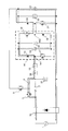
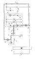
- FIG. 1 is a configuration diagram of a power conversion device according to Embodiment 1 of the present invention.
- the power conversion device includes elements from a diode bridge 12 as a rectifier circuit for full-wave rectification of an AC input from an AC power supply 1 to a smoothing capacitor 22 through a plurality of elements to be described later.
- the smoothing capacitor 22 side is viewed from the diode bridge 12, the side near the diode bridge 12, that is, the side far from the smoothing capacitor 22 is the previous stage, and the side far from the diode bridge 12, that is, the side close to the smoothing capacitor 22. Is referred to as the latter stage. Therefore, the smoothing capacitor 22 is disposed at the rearmost stage of the power conversion device.
- a charging relay 2 as a charging switch, a rectified current detection circuit 30 as a current detection means, and a reactor 13 as a current limiting means are sequentially connected in series.
- the inrush current prevention circuit 7 is configured by a series connection body of an inrush current prevention switch 3 and an inrush current prevention resistor 4, and is connected to the charging relay 2 in parallel.
- the inrush current prevention switch 3 is configured by a MOSFET in which a diode is connected in antiparallel, or an IGBT in which a diode is connected in antiparallel.
- the rectified voltage detection circuit 31 as voltage detection means is provided in parallel to the diode bridge 12.
- An inverter circuit 14 composed of a single-phase inverter is connected to the subsequent stage of the reactor 13 connected to the positive electrode side of the diode bridge 12.
- the inverter circuit 14 is connected to the first diode 15, the first semiconductor switch element 17 connected to the anode of the first diode 15, the second diode 16, and the cathode of the second diode 16.
- the second semiconductor switch element 18 is constituted by a bridge circuit.
- Each of the first semiconductor switch element 17 and the second semiconductor switch element 18 is configured by a MOSFET or IGBT in which diodes are connected in antiparallel.
- the inverter circuit 14 includes a first series circuit formed by connecting a first semiconductor switch element 17 and a first diode 15 in series, and a second semiconductor switch element 18 and a second diode 16 connected in series.
- the first series circuit and the second series circuit are connected in parallel, and the DC voltage source 19 includes the first series circuit and the first series circuit. It is connected between the parallel connection points of the series circuit and the second series circuit.
- One end 141 which is a connection point between the first semiconductor switch element 17 and the first diode 15 of the inverter circuit 14, is connected to the output terminal of the reactor 13 described above.
- the reactor 13 described above may be connected in series to the subsequent stage of the inverter circuit 14.
- the other end 142 which is a connection point between the second semiconductor switch element 18 and the second diode 16 of the inverter circuit 14 is connected to one end of the short-circuit switch 21 and the anode of the rectifier diode 20 as a rectifier element.
- the positive electrode that is one end of the smoothing capacitor 22 is connected to the cathode of the rectifier diode 20 and one end of the discharge switch 5 described later.
- the negative electrode that is the other end of the smoothing capacitor 22 is connected to the other end of the short-circuit switch 21 and the diode bridge 12. Each is connected to the negative terminal.
- a smoothing capacitor voltage detection circuit 33 as voltage detecting means is connected to the smoothing capacitor 22 in parallel.
- the short-circuit switch 21 is composed of a MOSFET or IGBT having diodes connected in antiparallel.
- the discharge switch 5 is connected to the positive electrode of the smoothing capacitor 22 and the cathode of the rectifier diode 20, and the other end is connected to a connection point between the inrush current prevention resistor 4 and the inrush current prevention switch 3.
- the discharge switch 5 is composed of a MOSFET or IGBT having diodes connected in antiparallel.
- the rectification current detection circuit 30 as current detection means inputs the detection value of the output current of the diode bridge 12 to the control unit 6 via the signal line 41b, and the rectification voltage detection circuit 31 detects the output voltage of the diode bridge 12. The value is input to the control unit 6 through the control line 41a.
- the DC voltage source voltage detection circuit 32 inputs the detected value of the voltage of the DC voltage source 19 to the control unit 6 via the control line 41c, and the smoothing capacitor voltage detection circuit 33 detects the detected value of the voltage of the smoothing capacitor 22. Is input to the control unit 6 through the control line 41d.
- the control unit 6 also includes a discharge switch 5, an inrush current prevention switch 3, a first semiconductor switch 17, a second semiconductor switch element 18, and a control line 40a, 40b, 40d, 40e, and 40f, respectively. Connected to the gate terminal of the short-circuit switch 21, the discharge switch 5, the inrush current prevention switch 3, the first semiconductor switch 17, the second semiconductor switch element 18, and the on-off control of the short-circuit switch 21 are performed.
- short circuit switch 21 showed what comprised the diode or MOSFET by which antiparallel connection was carried out, it is not restricted to this, A mechanical switch etc. may be sufficient.
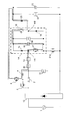
- FIG. 2 is an explanatory diagram for explaining an inrush current preventing operation in the power conversion device according to the first embodiment of the present invention.
- the charging relay 2 When the operation is started, the charging relay 2 is turned off and the inrush current prevention switch 3 is turned on, so that the AC power source 1, the diode bridge 12, the inrush current prevention switch 3, the inrush current prevention resistor as shown by a thick solid line in FIG. 4, an inrush current flows through a path that sequentially passes through the reactor 13, the first diode 14 of the inverter 14, the second semiconductor switch 18, the rectifier diode 20, the smoothing capacitor 22, and the diode bridge 12. This inrush current is reduced by the inrush current preventing resistor 4.
- control unit 6 determines the voltage value of the DC voltage source 19 and the voltage value of the smoothing capacitor 22 input from the DC voltage source voltage detection circuit 32 and the smoothing capacitor voltage detection circuit 33 via the control lines 41c and 41d.
- the charging relay 2 is turned on via the control line 40c, the inrush current prevention switch 3 is turned off via the control line 40d, and the power conversion operation is started.
- FIG. 3 is an explanatory diagram showing a path of a current flowing during a power conversion operation in the power conversion device according to the first embodiment of the present invention.
- the path through which the current flows is changed to a path indicated by a thick solid line in FIG. 3 or a part of the thick solid line indicated by a dotted line.
- the AC power source 1, the diode bridge 12, the reactor 13, the inverter circuit 14, the smoothing capacitor 22, the diode bridge 12, and the AC power source 1 are routed, and the following normal power conversion operation is performed.
- the output of the AC power source 1 that is full-wave rectified by the diode bridge 12 is connected to one end 141 of the inverter circuit 14 via the charging relay 2.
- the peak value of the input voltage input to the inverter circuit 14 is set to a value slightly higher than the DC voltage of the smoothing capacitor 22 controlled to the target voltage.
- the control unit 6 when the control unit 6 turns off both the first semiconductor switch element 17 and the second semiconductor switch 18 of the inverter circuit 14 via the control lines 40d and 40e, the input current from the diode bridge 12 is changed to the reactor 13
- the DC voltage source 19 is charged from one end 141 of the inverter circuit 14 via the first diode 15 via the first and the other end 142.
- the control unit 6 turns on only the first semiconductor switch element 17, the input current from the diode bridge 12 passes through the first semiconductor switch element 17 and the second diode 16 and the inverter circuit 14. Is output from the other end 142.
- the input current input from the diode bridge 12 to the one end 141 of the inverter circuit 14 is the same as that of the first diode 15 and the first diode 15.
- the signal is output from the other end 142 of the inverter circuit 14 via the second semiconductor switch element 18.
- the controller 6 simultaneously turns on the first semiconductor switch element 17 and the second semiconductor switch element 18, the input current input from the diode bridge 12 to the one end 141 of the inverter circuit 14 is the first current switch element 17.
- the DC voltage source 19 is discharged via the semiconductor switch 17 and output from the output terminal 142 via the second semiconductor switch 18.
- the control unit 16 performs four types of combination control of the first semiconductor switch element 17 and the second semiconductor switch element 18. Then, the control unit 6 controls the input current so that the input power factor from the AC power supply 1 is approximately “1” by PWM control of the inverter circuit 14 and superimposes the generated voltage of the inverter 14 on the input voltage. .
- the short-circuit switch 21 is controlled by the control unit 6 through the control line 40f so that the short-circuit switch 21 is turned on only in the short-circuit phase range centered on the zero-cross phase of the input voltage and input current.
- the power conversion apparatus according to Embodiment 1 of the present invention operates to improve the input power factor and reduce power loss and noise by such control.
- the smoothing capacitor 22 when a voltage equal to or higher than the rated voltage of the DC voltage source 19 is applied to the smoothing capacitor 22, if the DC voltage source 19 and the smoothing capacitor 22 are simultaneously discharged, the voltage of the smoothing capacitor 22 is applied to the DC voltage source 19. As a result, the DC voltage source 19 and surrounding elements may be destroyed due to over-rating, and in order to avoid this, it is necessary to increase the rating of the DC voltage source, etc. End up.
- the first semiconductor switch element 17, the second semiconductor switch element 18, and the short-circuit switch 21 are controlled as described below to prevent inrush current.
- the size of the resistor 4 is reduced.
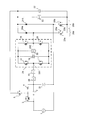
- FIG. 4 is an explanatory diagram showing a path of a current that flows when the smoothing capacitor is discharged in the power conversion device according to Embodiment 1 of the present invention. Shows the path flowing through the power conversion device according to Embodiment 1 of the present invention with a thick solid line.
- the control device 6 when discharging the smoothing capacitor 22 or the DC voltage source 19, as described above, the control device 6 first turns off the charging relay 2 and the inrush current prevention switch 3, respectively. The power is not supplied from the power source 1 to the power converter, and the discharge switch 5 is turned on. Next, the control device 6 turns on the first semiconductor switch element 17, turns off the second semiconductor switch 18, and turns on the short-circuit switch 21. As a result, as shown by a thick solid line in FIG. 4, the charge charged in the smoothing capacitor 22 is changed to the positive electrode of the smoothing capacitor 22, the discharge switch 5, the inrush current prevention resistor 4, the reactor 13, and the first semiconductor switch 17. The second capacitor 16, the short-circuit switch 21, and the negative electrode of the smoothing capacitor 22 flow in the first discharge path, and the smoothing capacitor 22 is discharged.
- This discharge path is also referred to herein as the first discharge path.
- FIG. 5 illustrates the path of the current that flows when the DC voltage source is discharged in the power converter according to Embodiment 1 of the present invention. It is a figure and the path
- the control unit 6 turns off the charging relay 2 and the inrush current prevention switch 3 and turns on the discharge switch 5.
- the control unit 6 turns on the first semiconductor switch element 17 and the second semiconductor switch 18 and turns off the short-circuit switch 21.
- the charge charged in the DC voltage source 19 is changed to the positive electrode of the DC voltage source 19, the second semiconductor switch element 18, the rectifier diode 20, the discharge switch 5, the inrush current.
- the current flows through a second discharge path configured in the order of the prevention resistor 4, the reactor 13, the first semiconductor switch element 17, and the negative electrode of the DC voltage source 19, and the DC voltage source 19 is discharged.
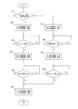
- FIG. 6 is a flowchart showing a discharge path switching determination algorithm in the power conversion device according to Embodiment 1 of the present invention.
- the determination algorithm shown in FIG. 6 corresponds to switching means in the control unit 6.
- step S ⁇ b> 1 it is determined whether or not the voltage value of the smoothing capacitor 22 is greater than the voltage value of the DC voltage source 19, and the voltage value of the smoothing capacitor 22 is greater than or equal to the voltage value of the DC voltage source 19. If it is determined (Yes), the process proceeds to step S2, and the power converter circuit is set so that the first discharge path is valid and the second discharge path is invalid. That is, as described above, the charging relay 2 and the inrush current prevention switch 3 are turned off, the discharge switch 5 is turned on, the first semiconductor switch element 17 is turned on, and the second semiconductor switch 18 is turned off. Then, the short-circuit switch 21 is turned on to form a first discharge path indicated by a thick solid line in FIG.
- the first semiconductor switch element 17 may be turned off and the second semiconductor switch element 18 may be turned on.
- a part of the first discharge path is a path indicated by a dotted line in FIG.
- step S3 it is determined whether or not the voltage value of the smoothing capacitor 22 is equal to or higher than a predetermined threshold value Vth as a predetermined value. If it is determined in step S3 that the voltage value of the smoothing capacitor 22 is less than the threshold value Vth (No), the process proceeds to step S4 so that the first discharge path is invalid and the second discharge path is valid.
- the circuit of the power converter that is, as described above, the charging relay 2 and the inrush current prevention switch 3 are turned off, the discharge switch 5 is turned on, the first semiconductor switch element 17 and the second semiconductor switch 18 are turned on, respectively.
- the short-circuit switch 21 is turned off, and a second discharge path indicated by a thick solid line in FIG. 5 is formed. As a result, the DC voltage source 19 discharges through the second discharge path.
- step S3 determines whether or not the voltage value of the smoothing capacitor 22 is greater than or equal to the threshold value Vth. If it is determined in step S5 that the voltage value of the DC voltage source 19 is less than the threshold value Vth (No), the process proceeds to step S6, where the first discharge path and the second discharge path are invalidated, and the discharge operation is performed. Exit. In order to invalidate both the first discharge path and the second discharge path, both the first semiconductor switch element 17 and the second semiconductor switch element 18 may be turned off. On the other hand, if it is determined in step S6 that the voltage value of the DC voltage source 19 is equal to or greater than the threshold value Vth (Yes), step S5 is repeated.
- step S7 When it is determined in step S1 that the voltage value of the smoothing capacitor 22 is less than the voltage value of the DC voltage source 19 (No), in step S7, the first discharge path is disabled, and the second The discharge path is enabled and the DC voltage source 19 starts to be discharged. That is, the charging relay 2 and the inrush current prevention switch 3 are turned off, the discharge switch 5 is turned on, the first semiconductor switch element 17 and the second semiconductor switch 18 are turned on, and the short-circuit switch 21 is turned on. And a second discharge path indicated by a thick solid line in FIG. 5 is formed. As a result, the DC voltage source 19 discharges through the second discharge path.
- step S8 it is determined whether or not the voltage value of the DC voltage source 19 is equal to or greater than a predetermined threshold value Vth. If it is determined in step S8 that the voltage value of the DC voltage source 19 is less than the threshold value Vth (No), the first discharge path is set valid and the second discharge path is set invalid in step S9.
- the discharge of the smoothing capacitor 22 is started. That is, as described above, the charging relay 2 and the inrush current prevention switch 3 are turned off, the discharge switch 5 is turned on, the first semiconductor switch element 17 is turned on, and the second semiconductor switch 18 is turned off. Then, the short-circuit switch 21 is turned on, the first discharge path indicated by the thick solid line in FIG. 4 is formed, and the smoothing capacitor 22 is discharged.
- step S8 determines whether or not the voltage value of the smoothing capacitor 22 is greater than or equal to a threshold value Vth. If it is determined in step S10 that the voltage value of the smoothing capacitor 22 is less than the threshold value Vth (No), the process proceeds to step S6, in which the first discharge path is disabled and the second discharge path is disabled. Exit. To disable the first discharge path and disable the second discharge path in step S6, it is possible to turn off the discharge switch S5 and the short-circuit switch S21. On the other hand, if it is determined in step S10 that the voltage value of the smoothing capacitor 22 is greater than or equal to the threshold value Vth (Yes), step S10 is repeated.
- the switching determination algorithm executed in the above-described control unit 6 is a flowchart when the voltage value is used as a threshold value.
- the present invention is not limited to this.
- switching determination is performed using the current value as a threshold value. May be. That is, the current detection means 30 for detecting the current flowing through the first discharge path and the second discharge path is provided, and the switching means in the control unit 6 is configured so that the first discharge path and the second discharge path are as described above.
- the current value detected by the current detection means 30 falls below a predetermined value after discharging one of the smoothing capacitor and the DC voltage source with either one of the discharge paths enabled.
- the discharge path is switched so as to invalidate one of the valid discharge paths and validate the other invalid discharge path.
- the inrush current preventing resistor 4 is connected in series between the output stage of the diode bridge 12 and the inverter circuit 14, but this is not limitative. Instead, it may be connected to the subsequent stage of the reactor 13 or the subsequent stage of the inverter circuit 14.
- the cathode side of the rectifier diode 20 is connected to the positive electrode of the smoothing capacitor 22. However, even if the anode side of the rectifier diode 20 is connected to the negative electrode side of the smoothing capacitor 22, An operation similar to that in the first embodiment can be obtained.
- the inverter circuit 14 is configured by one single-phase inverter.
- a plurality of single-phase inverters are connected in series.
- an inverter circuit may be configured. That is, FIG. 7 is a block diagram showing a modification of the power conversion device according to Embodiment 1 of the present invention.
- the inverter circuit 100 includes a first single-phase inverter 14a and a second single-phase inverter 14b.
- One end 14a1 of the first single-phase inverter 14a is connected to the subsequent stage of the reactor 13, and the other end 14a2 is connected to one end 14b1 of the second single-phase inverter 14b.
- a short-circuit switch 21 and a rectifier diode 20 are connected in parallel to the other end 14b2 of the second single-phase inverter 14b.
- the DC voltage source 19 of the first single-phase inverter 14a and the DC voltage source 19 of the second single-phase inverter 14b are set to the same voltage value.
- the 1st single phase inverter 14a and the 2nd single phase inverter 14b are mutually connected in series by the alternating current side terminal.
- Other configurations are the same as those in FIG.
- the smoothing capacitor 22 and the DC voltage sources 19 of the first single-phase inverter 14a and the second single-phase inverter 14b have different discharge paths. Since discharge is performed, it is necessary to switch the discharge path. The switching is basically the same as the discharge path switching determination algorithm shown in FIG. In the following description, the first discharge path in steps S2 and S9 shown in FIG. 6 is set to be valid, the second discharge path is set to be invalid, and the first discharge path in steps S4 and S7. Only the setting for invalidating the first discharge path and the setting for invalidating the first discharge path and the second discharge path in step S6 will be described.
- the charging relay 2 and the inrush current prevention switch 3 are turned off, and the discharge switch 5 is turned on.
- one of the first semiconductor switch element 17 and the second semiconductor switch element 18 in the first single-phase inverter 14a is turned on, the other is turned off, and the second single-phase inverter is turned on. This is performed by turning on one of the first semiconductor switch element 17 and the second semiconductor switch element 18 in 14b, turning the other off, and turning on the short-circuit switch 21.
- a first discharge path is formed without passing through the DC voltage source 19 of the first single-phase inverter 14a and the second single-phase inverter 14b, and the smoothing capacitor 22 starts discharging through the first discharge path. .
- the charging relay 2 and the inrush current prevention switch 3 are turned off, and the discharge switch 5 is turned off.
- the first semiconductor switch element 17 and the second semiconductor switch 18 of the first single-phase inverter 14a are simultaneously turned on, and the second single-phase inverter 14b is connected to the first semiconductor switch element 17 and the first semiconductor switch element 17a.
- One of the two semiconductor switch elements 18 is turned on, the other is turned off, and the short-circuit switch 21 is turned off.
- the DC voltage source 19 of the first single-phase inverter 14a forms a second discharge path without passing through the DC voltage source 19 of the second single-phase inverter 14b, and the first single-phase inverter 14a
- the discharge of the DC voltage source 19 can be started.
- the first semiconductor switch element 17 and the second semiconductor switch 18 of the second single-phase inverter 14b are turned on simultaneously, and the first semiconductor switch element 17 and the second semiconductor switch element 17 of the first single-phase inverter 14a are turned on.
- One of the semiconductor switch elements 18 is turned on and the other is turned off.
- the DC voltage source 19 of the second single-phase inverter 14b can be discharged through the second discharge path without passing through the DC voltage source 19 of the first single-phase inverter 14b.
- the single-phase inverters 14a and 14b are turned on simultaneously. However, in this case, since the discharge current becomes large, the DC voltage sources of the first single-phase inverter 14a and the second single-phase inverter 14b as described above. Should be discharged separately.
- step S6 in order to invalidate the first discharge path and invalidate the second discharge path in step S6, the discharge switch S5 and the short-circuit switch S21 can be turned off, respectively.
- the inrush current preventing resistor 4 is connected in series between the output stage of the diode bridge 12 and the inverter circuit 14, but the present invention is not limited to this. For example, you may connect in series between the 1 single phase inverter 14a and the 2nd single phase inverter 14b.
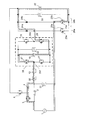
- FIG. FIG. 8 is a configuration diagram of a power conversion device according to Embodiment 2 of the present invention.
- the power conversion device according to the second embodiment of the present invention is the same as the power conversion device according to the first embodiment except for the connection position of the short-circuit switch 21a.
- a short-circuit switch 21 a is connected between the negative electrode of the DC voltage source 19 and the negative electrode of the smoothing capacitor 22 in the inverter circuit 14. Yes.
- one end of the short-circuit switch 21 a is connected to the negative electrode of the DC voltage source 19, and the other end of the short-circuit switch 21 a is connected to the negative electrode of the diode bridge 12 and the negative electrode of the smoothing capacitor 22.
- FIG. 9 is an explanatory diagram showing a path of a current that flows when the smoothing capacitor is discharged in the power conversion device according to the second embodiment of the present invention.
- the control unit 6 turns off the charging relay 2 and the inrush current prevention switch 3, turns on the discharge switch 5, and the first semiconductor switch element of the inverter circuit 14. 17 is turned on, the second semiconductor switch element 18 is turned off, and the short-circuit switch element 21a is turned on.
- FIG. 10 is an explanatory diagram showing a path of a current that flows when the DC voltage source is discharged in the power conversion device according to the second embodiment of the present invention.
- the control unit 6 turns off the charging relay 2 and the inrush current prevention switch 3, turns on the discharge switch 5, and switches the first semiconductor switch element 17 and the first semiconductor switch element 17.
- the two semiconductor switches 18 are turned on, and the short-circuit switch 21a is turned off. Accordingly, as shown by a thick solid line in FIG.
- the positive electrode of the DC voltage source 19 the positive electrode of the DC voltage source 19, the second semiconductor switch element 18, the rectifier diode 20, the discharge switch 5, the inrush current preventing resistor 4, the reactor 13, and the first semiconductor switch.
- the charge charged in the DC voltage source 19 flows through the second discharge path constituted by the element 17 and the negative electrode of the DC voltage source 19, and the DC voltage source 19 is discharged.
- the power conversion device according to the second embodiment of the present invention can achieve the same effect as the power conversion device according to the first embodiment described above, and since the short-circuit switch 21a is connected to the negative electrode side of the DC voltage source 19, the short-circuit switch 21a It is possible to reduce the number of circuit elements through which a current passes when is turned on, and to reduce the burden on the circuit elements during discharging. Further, the conduction loss can be reduced as a power converter, and as a result, the conversion efficiency of the entire power converter can be improved.
- the inverter circuit 14 is composed of one single-phase inverter.
- a plurality of single-phase inverters are connected in series.
- an inverter circuit may be configured. That is, FIG. 11 is a block diagram showing a modification of the power conversion device according to Embodiment 2 of the present invention.
- the inverter circuit 100 includes a first single-phase inverter 14a and a second single-phase inverter 14b.
- One end 14a1 of the first single-phase inverter 14a is connected to the subsequent stage of the reactor 13, and the other end 14a2 is connected to one end 14b1 of the second single-phase inverter 14b.
- the anode of the rectifier diode 20 is connected to the other end 14b2 of the second single-phase inverter 14b.
- the first single-phase inverter 14a and the second single-phase inverter 14b are connected to each other at their AC terminals.
- the DC voltage source 19 of the first single-phase inverter 14a and the DC voltage source 19 of the second single-phase inverter 14b are set to the same voltage value.
- the inverter circuit 100 when the inverter circuit 100 is configured by connecting a plurality of single-phase inverters 14a and 14b in series, the single-phase inverter connected to the final stage among the plurality of single-phase inverters 14a and 14b.
- the short-circuit switch 21a By connecting the short-circuit switch 21a to the negative electrode side of the DC voltage source 19 in the inverter 14b, the same operation as in the case of FIG.
- the first single-phase inverter 14a and the first single-phase inverter 14a and the second single-phase inverter 14b are discharged when the smoothing capacitor 22 is discharged and when the DC voltage source 19 of the first single-phase inverter 14a and the second single-phase inverter 14b are discharged.
- On / off control of the first semiconductor switch element 17 and the second semiconductor switch element 18 of the two single-phase inverters 14b is the same as in the case of FIG.
- the inrush current prevention circuit 7 is connected in series to the output stage of the diode bridge 12, but the present invention is not limited to this.
- the first single phase You may connect in series between the inverter 14a and the 2nd single phase inverter 14b.
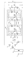
- FIG. 12 is a configuration diagram of a power conversion device according to Embodiment 3 of the present invention.
- the power converter according to Embodiment 3 of the present invention does not include the diode bridge 12 as in Embodiments 1 and 2, and one end of the AC power supply 1 is charged.
- the inrush current prevention switch 3 and the inrush current prevention resistor 4 are directly connected to the relay 2 and are connected in parallel with the charging relay 2.
- the output stage of the charging relay 2 is connected to the rectified current detection circuit 30 and the reactor 13, and one end 291 of an inverter circuit 29 configured by a single-phase inverter is connected in series to the subsequent stage.
- the rectified voltage detection circuit 31 is provided in parallel with the AC power supply 1.
- the inverter circuit 29 includes a first semiconductor switch element 17, a second semiconductor switch element 18, and a third semiconductor switch made of an IGBT in which diodes are connected in antiparallel, a MOSFET in which a diode is built in between source and drain, and the like. It is composed of an element 27, a fourth semiconductor switch element 28, and a DC power source 19.
- a DC voltage source voltage detection circuit 32 is connected in parallel with the DC voltage source 19.
- the other end 292 of the inverter circuit 29 is connected to a series connection point of a first short-circuit switch 23a made of a semiconductor switch element such as a MOSFET to which a diode 25a is connected in antiparallel, and a first rectifier diode 24a. Furthermore, a series connection point of the second short-circuit switch 23 b made of a semiconductor switch element such as a MOSFET to which the diode 25 b is connected in anti-parallel is connected to the other end of the AC power supply 1.
- the first short-circuit switch 23a and the first rectifier diode 24a constitute a first series circuit 26a
- the second short-circuit switch element 23b and the second rectifier diode 24b constitute a second series circuit 26b.
- the first series circuit 26a and the second series circuit 26b are connected in parallel, and both terminals of the smoothing capacitor 22 are connected to the output stage.
- a smoothing capacitor voltage detection circuit 33 is connected in parallel to the smoothing capacitor 22.
- the first short-circuit switch 23a and the second short-circuit switch 23b are not limited to semiconductor switch elements, and may be configured by mechanical switches or the like. In this case, the diodes 25a and 25b are reversed. Connect in parallel.
- the power converter according to Embodiment 3 of the present invention differs from the power converter according to Embodiment 1 and Embodiment 2 in the configuration of a short-circuit switch or the like, but is otherwise the same.
- FIG. 13 is an explanatory diagram for explaining an inrush current preventing operation in the power conversion device according to the third embodiment of the present invention, and shows a path through which a current flows immediately after the operation is started by a thick solid line.
- the charge relay 2 and the discharge switch 5 are turned off, the first semiconductor switch element 27 and the second semiconductor switch 28 are turned on, and the third semiconductor switch element 17 and the fourth semiconductor switch are turned on.
- the semiconductor switch 18 is turned off, the second short-circuit switch 23b is turned on, and the first short-circuit switch 23a is turned off. In this state, the inrush current prevention switch 3 is turned on.
- the inrush current is reduced by the inrush current preventing resistor 4.
- the charging relay 2 is turned on, the inrush current prevention switch 3 is turned off, the third semiconductor switch element 27 is turned off, the first semiconductor switch element 17 is turned on, and the first short-circuit switch 23a is turned on.
- the path through which the current flows from the AC power source 1 is the AC power source 1, the charging relay 2, the reactor 13, the first semiconductor switch element 17, the fourth semiconductor switch element 28, the first short-circuit switch 23a, and the second short-circuit switch. 23b, the path is changed to the AC power source 1.
- FIG. 14 is an explanatory diagram showing a path of a current that flows when the smoothing capacitor is discharged in the power conversion device according to Embodiment 3 of the present invention.
- the charge relay 2 and the inrush current prevention switch 3 are turned off, the discharge switch 5 is turned on, the first semiconductor switch element 17 and the fourth semiconductor switch 28 are turned on, and the second semiconductor switch element 18
- the third semiconductor switch 27 is turned off, the first short-circuit switch 23a is turned on, and the second short-circuit switch 23b is turned off.
- the electric charge charged in the smoothing capacitor 22 is changed to the positive electrode of the smoothing capacitor 22, the discharge switch 5, the inrush current prevention resistor 4, the reactor 13, and the first semiconductor switch element 17. Then, the fourth semiconductor switch element 28, the first short-circuit switch 23a, and the negative electrode of the smoothing capacitor 22 flow through the first discharge path, and the smoothing capacitor 22 is discharged.
- FIG. 15 is an explanatory diagram showing a path of a current that flows when the DC voltage source is discharged in the power conversion device according to Embodiment 3 of the present invention.
- the charging relay 2 and the inrush current prevention switch 3 are turned off, the discharge switch 5 is turned on, and the first semiconductor switch element 17 and the second semiconductor switch element 18 are turned on.
- the third semiconductor switch element 27 and the fourth semiconductor switch element 28 are turned off, respectively, and the first short circuit switch 23a and the second short circuit switch 23b are turned off.
- the charge charged in the DC voltage source 19 is changed to the positive electrode of the DC voltage source 19, the second semiconductor switch element 18, the first rectifier diode 24 a, and the discharge switch 5.
- the same effect as in the first embodiment can be obtained, and further, the diode bridge 12 used in the first embodiment is unnecessary, so that the number of parts can be reduced and the device configuration can be simplified. Become. Further, since the number of elements through which current passes can be reduced, conduction loss can be reduced, and the conversion efficiency of the entire power conversion device can be improved.
- the inverter circuit 100 may be configured by connecting a plurality of single-phase inverters in series as shown in FIG. good.
- the inrush current preventing resistor 4 may be connected in series between the first single-phase inverter 14a and the second inverter 14b.
- the rectifier diodes 20, 24a, and 24b are connected to the smoothing capacitor 22 as rectifier elements.
- a semiconductor switch is connected, and the same is achieved by on / off control. You may make it operate
- one end of the discharge switch 5 is connected to the positive electrode side of the smoothing capacitor 22, but the present invention is not limited to this, and may be connected to the negative electrode side of the smoothing capacitor 22.
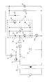
- FIG. 16 is a configuration diagram of a power conversion device according to Embodiment 4 of the present invention.
- an inverter circuit constituted by a single-phase inverter is provided.
- a fourth embodiment includes a PFC (Power Factor Correction) converter.
- an IGBT in which a diode is connected in antiparallel
- a semiconductor switch element 42 made up of a MOSFET in which a diode is built in between source and drain
- a diode 41 connected between the two forms a PFC converter.
- Other configurations are the same as those of the above-described embodiment.
- the control unit 6 turns off the charging relay 2, turns off the discharge switch 5, and prevents inrush current. Turn on the switch. Thereby, the inrush current from the diode bridge 12 is prevented. Thereafter, when it is determined that the voltage value of the smoothing capacitor 22 detected by the smoothing capacitor voltage detection circuit 33 is equal to or higher than a predetermined voltage value, the control unit 6 turns on the charging relay 2 and turns off the inrush current prevention switch 3. Then, the discharge switch 5 is turned off. Thereby, the smoothing capacitor 22 is charged through the charging path of the AC power source 1, the diode bridge 12, the charging resistor 2, the reactor 40, the rectifier diode 41, the smoothing capacitor 22, the diode bridge 12, and the AC power source 1.
- the control unit 6 turns off the charging relay 2, turns off the inrush current prevention switch 3, and turns on the discharging switch 5. And thereby, the charge stored in the smoothing capacitor 22 is formed in the order of the positive electrode of the smoothing capacitor 22, the discharge switch 5, the inrush current prevention resistor 4, the reactor 40, the semiconductor switch element 42, and the negative electrode of the smoothing capacitor 22. 5, the smoothing capacitor 22 is discharged.
- the same effects as those of the first embodiment described above can be obtained, and the number of parts can be reduced, thereby simplifying the apparatus configuration. Moreover, since the number of elements through which current passes can be reduced, conduction loss can be reduced, and the conversion efficiency of the entire power conversion device can be improved.
- the present invention can be used in the field of power conversion devices that convert alternating current power into direct current power, and is particularly useful in the field of in-vehicle power conversion devices mounted on vehicles such as automobiles, and further in the automobile industry and the like. is there.
Abstract
【課題】構成部品の数を減らし、小型且つ安価な電力変換装置を提供する。 【構成】交流電源1の後段に接続されインバータ回路14と、前記インバータ回路14の後段に整流素子20を介して接続された平滑コンデンサ22と、前記インバータ回路14の前段に接続され、オンのとき前記交流電源1の出力に基づく電気量を前記インバータ回路14へ入力し、オフのとき前記インバータ回路14への前記電気量の入力を遮断する充電スイッチ2と、突入電流防止スイッチ3と前記突入電流防止スイッチ3の後段に直列接続された突入電流防止抵抗4とを有する突入電流防止回路7とを備え、前記突入電流防止回路7は、前記充電スイッチ2に並列接続されていることを特徴とする。
Description
この発明は、交流電力を直流電力に変換する電力変換装置、更に詳しくは、入力力率を改善する回路を備えた電力変換装置に関するものである。
従来の電力変換装置としては、特許文献1に開示されている技術が知られている。この従来の電力変換装置は、図17に示すように、交流電源1にメインリレー10を介して接続されるダイオードブリッジ12と、ダイオードブリッジ12の後段に突入電流防止抵抗4とリアクトル13を介して接続され、直流電圧源19とダイオード15、16、及び半導体スイッチ素子17、18からなる単相インバータにより構成されたインバータ回路14と、インバータ回路14の後段に整流ダイオード20と短絡スイッチ21を介して接続された平滑コンデンサ22とを備えている。
突入電流防止抵抗4には充電リレー2aが並列接続されている。又、平滑コンデンサ22の正極は、放電抵抗11と放電リレー5aを介して突入電流防止抵抗4とリアクトル13との間に接続されている。尚、31は整流電圧検出回路、32は直流電圧検出回路、33は平滑コンデンサ電圧検出回路である。
このように構成された従来の電力変換装置に於いて、交流電源1からの交流入力は、ダイオードブリッジ12により全波整流され、リアクトル13を介してインバータ回路14に入力される。インバータ回路14は、交流電源1からの入力力率が概ね「1」になるようにダイオードブリッジ12からの入力電流をPWM制御し、直流電圧源19にエネルギーを蓄積すると共に平滑コンデンサ22の直流電圧を所定の目標電圧に追随させる。このような従来の電力変換装置によれば、入力力率の改善、電力損失及びノイズの低減化を図ることができる。
しかしながら、前述の従来の電力変換装置は、平滑コンデンサ22を充電する充電動作を行なうためには、交流電源1と電力変換装置との間を遮断又は接続するためのメインリレー10と、動作開始時の突入電流を防止する突入電流防止抵抗4をバイパスするための充電リレー2aとの、2つのリレーを必要としている。
一般に、電子部品に対してシロキサンが不具合を誘発する例としてはリレーの接点不良が多く、密閉された部品に低分子シロキサンを発生させるシリコーンを使用していると、部品の動作熱によりシロキサンが発生し、リレー接点上に付着する。特にオン/オフ回数の多いリレー接点では、常時、接点に衝撃が与えられるので、接点の表面に付着したシロキサンが酸化分解して二酸化珪素(SiO2)となり、これが電気絶縁物として作用して接点障害を引き起こすという課題がある。例えば、部品の接着剤や放熱シートにシリコーンを含有する素材を使用している場合に前述の課題が発生する。このため、リレーは極力使用しないほうがよいとされている。
一方、リレーの代わりにMOSFET(Metal Oxide Semiconductor Field Effect Transistor)、或いはIGBT(Insulated Gate Bipolar Transistor)等の半導体素子をスイッチとして使用すると、半導体スイッチ素子のオン抵抗はリレーのオン抵抗に比べて高いため、電力損失が大きくなってしまう。従って、電力変換装置の高効率化のためには半導体スイッチ素子よりリレーを使用した方がよい。
又、前述の従来の電力変換装置は、動作開始時の突入電流を防止するための突入電流防止抵抗4と動作終了時の平滑コンデンサ22に蓄えられた電荷を放電するための放電抵抗11を夫々設ける必要があり、各抵抗はコストが高く、さらに通常の動作時は使用しないため無駄である。このため、電力変換装置が大型化し、製造コストが高くなるという課題があった。
この発明は、従来の電力変換装置に於ける前述のような課題を解消するために成されたものであって、構成部品の数を減らし、小型且つ安価な電力変換装置を提供することを目的とする。
この発明による電力変換装置は、交流電源の後段に接続されインバータ回路と、前記インバータ回路の後段に整流ダイオードを介して接続された平滑コンデンサと、前記インバータ回路の前段に接続され、オンのとき前記交流電源の出力に基づく電気量を前記インバータ回路へ入力し、オフのとき前記インバータ回路への前記電気量の入力を遮断する充電スイッチと、突入電流防止スイッチと、前記突入電流防止スイッチの後段に直列接続された突入電流防止抵抗とを有する突入電流防止回路とを備え、前記突入電流防止回路は、前記充電スイッチに並列接続されていることを特徴とするものである。
又、この発明による電力変換装置は、交流電源の後段に接続され前記交流電源の出力を整流する整流回路と、前記整流回路の出力端子間に接続された半導体スイッチ素子とにより構成されたAC/DCコンバータと、前記AC/DCコンバータの後段に整流ダイオードを介して接続された平滑コンデンサと、前記整流回路の後段と前記半導体スイッチ素子との間に接続され、オンのとき前記整流回路の出力を前記半導体アスイッチ素子へ入力し、オフのとき前記半導体スイッチ素子への入力を遮断する充電スイッチと、突入電流防止スイッチと、前記突入電流防止スイッチの後段に接続された抵抗とを有する突入電流防止回路とを備え、前記突入電流防止回路は、前記充電スイッチに並列接続されていることを特徴とするものである。
この発明による電力変換装置は、交流電源の後段に接続されインバータ回路と、前記インバータ回路の後段に整流ダイオードを介して接続された平滑コンデンサと、前記インバータ回路の前段に接続され、オンのとき前記交流電源の出力に基づく電気量を前記インバータ回路へ入力し、オフのとき前記インバータ回路への前記電気量の入力を遮断する充電スイッチと、突入電流防止スイッチと、前記突入電流防止スイッチの後段に直列接続された突入電流防止抵抗とを有する突入電流防止回路とを備え、前記突入電流防止回路は、前記充電スイッチに並列接続されているので、突入電流防止スイッチに半導体スイッチ素子を使用することができ、又、電力変換時に使用する充電スイッチを1つにする構成をとることができ、低分子シロキサンによるリレーの接点不良の問題を軽減し、回路の安全性の向上、大規模化及びコストアップの防止を図ることができる。
又、この発明による電力変換装置は、交流電源の後段に接続され前記交流電源の出力を整流する整流回路と、前記整流回路の出力端子間に接続された半導体スイッチ素子とにより構成されたAC/DCコンバータと、前記AC/DCコンバータの後段に整流ダイオードを介して接続された平滑コンデンサと、前記整流回路の後段と前記半導体スイッチ素子との間に接続され、オンのとき前記整流回路の出力を前記半導体アスイッチ素子へ入力し、オフのとき前記半導体スイッチ素子への入力を遮断する充電スイッチと、突入電流防止スイッチと、前記突入電流防止スイッチの後段に接続された抵抗とを有する突入電流防止回路とを備え、前記突入電流防止回路は、前記充電スイッチに並列接続されているので、突入電流防止スイッチに半導体スイッチ素子を使用することができ、又、電力変換時に使用する充電スイッチを1つにする構成をとることができ、低分子シロキサンによるリレーの接点不良の問題を軽減し、回路の安全性の向上、大規模化及びコストアップの防止を図ることができる。
実施の形態1.
以下、この発明の実施の形態1による電力変換装置について説明する。図1はこの発明の実施の形態1による電力変換装置の構成図である。図1に於いて、電力変換装置は、交流電源1からの交流入力を全波整流する整流回路としてのダイオードブリッジ12から後述する複数の要素を経て平滑コンデンサ22までの要素で構成されている。以下の説明に於いて、ダイオードブリッジ12から平滑コンデンサ22側を見て、ダイオードブリッジ12に近い側、つまり平滑コンデンサ22から遠い側を前段、ダイオードブリッジ12から遠い側、つまり平滑コンデンサ22に近い側を後段、と称する。従って、平滑コンデンサ22は、電力変換装置の最も後段に配設されていることになる。
以下、この発明の実施の形態1による電力変換装置について説明する。図1はこの発明の実施の形態1による電力変換装置の構成図である。図1に於いて、電力変換装置は、交流電源1からの交流入力を全波整流する整流回路としてのダイオードブリッジ12から後述する複数の要素を経て平滑コンデンサ22までの要素で構成されている。以下の説明に於いて、ダイオードブリッジ12から平滑コンデンサ22側を見て、ダイオードブリッジ12に近い側、つまり平滑コンデンサ22から遠い側を前段、ダイオードブリッジ12から遠い側、つまり平滑コンデンサ22に近い側を後段、と称する。従って、平滑コンデンサ22は、電力変換装置の最も後段に配設されていることになる。
ダイオードブリッジ12の後段には、充電スイッチとしての充電リレー2、電流検出手段としての整流電流検出回路30、限流手段としてのリアクトル13が、順次直列に接続されている。突入電流防止回路7は、突入電流防止スイッチ3と突入電流防止抵抗4との直列接続体により構成され、充電リレー2に並列に接続されている。突入電流防止スイッチ3は、ダイオードが逆並列に接続されたMOSFET、若しくはダイオードが逆並列に接続されたIGBTにより構成されている。電圧検出手段としての整流電圧検出回路31は、ダイオードブリッジ12に対して並列に設けられている。
ダイオードブリッジ12の正極側に接続されたリアクトル13の後段には、単相インバータにより構成されたインバータ回路14が接続されている。インバータ回路14は、第1のダイオード15と、この第1のダイオード15のアノードに接続された第1の半導体スイッチ素子17と、第2のダイオード16と、この第2のダイオード16のカソードに接続された第2の半導体スイッチ素子18とから成るブリッジ回路により構成されている。第1の半導体スイッチ素子17と第2の半導体スイッチ素子18は、夫々、ダイオードが逆並列に接続されたMOSFET若しくはIGBTにより構成されている。
インバータ回路14は、第1の半導体スイッチ素子17と第1のダイオード15とを直列接続してなる第1の直列回路と、第2の半導体スイッチ素子18と第2のダイオード16とを直列接続してなる第2の直列回路と、直流電圧源19とを備えた単相インバータ回路により構成され、第1の直列回路と第2の直列回路は並列接続され、直流電圧源19は、第1の直列回路と第2の直列回路の並列接続点の間に接続されている。
インバータ回路14の第1の半導体スイッチ素子17と第1のダイオード15との接続点である一端141は、前述のリアクトル13の出力端に接続されている。尚、前述のリアクトル13は、インバータ回路14の後段に直列接続されてもよい。
インバータ回路14の第2の半導体スイッチ素子18と第2のダイオード16との接続点である他端142は、短絡スイッチ21の一端と整流素子としての整流ダイオード20のアノードに接続されている。平滑コンデンサ22の一端である正極は、整流ダイオード20のカソードと後述する放電スイッチ5の一端に夫々接続され、平滑コンデンサ22の他端である負極は、短絡スイッチ21の他端とダイオードブリッジ12の負極側端子に夫々接続されている。電圧検出手段としての平滑コンデンサ電圧検出回路33は、平滑コンデンサ22に並列に接続されている。尚、短絡スイッチ21は、ダイオードが逆並列に接続されたMOSFET若しくはIGBTにより構成されている。
放電スイッチ5の一端は、平滑コンデンサ22の正極と整流ダイオード20のカソードに接続され、他端は、突入電流防止抵抗4と突入電流防止スイッチ3との接続点に接続されている。放電スイッチ5は、ダイオードが逆並列に接続されたMOSFET若しくはIGBTにより構成されている。
電流検出手段としての整流電流検出回路30は、ダイオードブリッジ12の出力電流の検出値を信号線41bを介して制御部6に入力し、整流電圧検出回路31は、ダイオードブリッジ12の出力電圧の検出値を制御線41aを介して制御部6に入力する。又、直流電圧源電圧検出回路32は、直流電圧源19の電圧の検出値を制御線41cを介して制御部6に入力し、平滑コンデンサ電圧検出回路33は、平滑コンデンサ22の電圧の検出値を制御線41dを介して制御部6に入力する。
又、制御部6は、制御線40a、40b、40d、40e、40fを介して、夫々、放電スイッチ5、突入電流防止スイッチ3、第1の半導体スイッチ17、第2の半導体スイッチ素子18、及び短絡スイッチ21のゲート端子に接続されており、放電スイッチ5、突入電流防止スイッチ3、第1の半導体スイッチ17、第2の半導体スイッチ素子18、及び短絡スイッチ21のオン/オフの制御を行う。
尚、短絡スイッチ21は、ダイオードが逆並列接続されたMOSFET若しくはIGBTにより構成したものを示したが、これに限るものではなく、機械式のスイッチ等であっても良い。
次に、この発明の実施の形態1による電力変換装置の動作を説明する。電力変換装置の動作開始時である起動時に於いて、交流電源1を投入した直後は電力変換装置に突入電流が流れるため、制御部6は制御線40cを介して充電リレー2をオフとし、制御線40bを介して突入電流防止スイッチ3をオンとする。図2は、この発明の実施の形態1による電力変換装置に於ける、突入電流防止動作を説明する説明図である。動作開始時には充電リレー2をオフとし、突入電流防止スイッチ3をオンとすることにより、図2に太い実線で示すように、交流電源1、ダイオードブリッジ12、突入電流防止スイッチ3、突入電流防止抵抗4、リアクトル13、インバータ14の第1のダイオード14、第2の半導体スイッチ18、整流ダイオード20、平滑コンデンサ22、及びダイオードブリッジ12を順次経由する経路で突入電流が流れる。この突入電流は、突入電流防止抵抗4により低減される。
次に、制御部6は、制御線41c、41dを介して直流電圧源電圧検出回路32、及び平滑コンデンサ電圧検出回路33から入力された直流電圧源19の電圧値、及び平滑コンデンサ22の電圧値が、所定値以上であることを確認して後、制御線40cを介して充電リレー2をオンとし、制御線40dを介して突入電流防止スイッチ3をオフとして電力変換動作に入る。
図3は、この発明の実施の形態1による電力変換装置に於ける、電力変換動作時に流れる電流の経路を示す説明図である。充電リレー2をオンとし、突入電流防止スイッチ3をオフにすることにより、電流の流れる経路が、図3に太い実線で示す経路、又は太い実線の一部が点線で示す経路に変更された経路で示すように、交流電源1、ダイオードブリッジ12、リアクトル13、インバータ回路14、平滑コンデンサ22、ダイオードブリッジ12、及び交流電源1に至る経路となり、次に述べる通常の電力変換動作が行なわれる。
即ち、充電リレー2がオンとなり突入電流防止スイッチ3がオフとなることにより、ダイオードブリッジ12により全波整流された交流電源1の出力は、充電リレー2を介してインバータ回路14の一端141と、平滑コンデンサ22の負極間に印加される。尚、インバータ回路14に入力される入力電圧のピーク値は、目標電圧に制御される平滑コンデンサ22の直流電圧よりも僅かに高い値に設定されている。
ここで、制御部6が制御線40d、40eを介してインバータ回路14の第1の半導体スイッチ素子17と第2の半導体スイッチ18を共にオフにすると、ダイオードブリッジ12からの入力電流は、リアクトル13を介してインバータ回路14の一端141から第1のダイオード15を経由して直流電圧源19を充電し、他端142から出力される。又、制御部6が第1の半導体スイッチ素子17のみをオンとしたときは、ダイオードブリッジ12からの入力電流は、第1の半導体スイッチ素子17と第2のダイオード16を経由してインバータ回路14の他端142から出力される。
更に、制御部6がインバータ回路14の第2の半導体スイッチ素子18のみをオンとしたときは、ダイオードブリッジ12からインバータ回路14の一端141に入力された入力電流は、第1のダイオード15と第2の半導体スイッチ素子18を経由して、インバータ回路14の他端142から出力される。又、制御部6が第1の半導体スイッチ素子17と第2の半導体スイッチ素子18を同時にオンとしたときは、ダイオードブリッジ12からインバータ回路14の一端141に入力された入力電流は、第1の半導体スイッチ17を経由して直流電圧源19を放電し、第2の半導体スイッチ18を経由して出力端142から出力される。
このように、制御部16は、第1の半導体スイッチ素子17と第2の半導体スイッチ素子18の4種類の組み合わせ制御を行なう。そして、制御部6は、インバータ回路14のPWM制御により、交流電源1からの入力力率が概ね「1」となるように入力電流を制御すると共に、インバータ14の発生電圧を入力電圧に重畳させる。短絡スイッチ21は、入力電圧及び入力電流のゼロクロス位相を中央とする短絡位相範囲でのみオンとなるように、制御線40fを介して制御部6により制御され、平滑コンデンサ22の直流電圧を所定の目標電圧に追従させる。この発明の実施の形態1による電力変換装置は、このような制御により、入力力率の改善、及び電力損失及びノイズの低減化を図るように動作する。
次に、この発明の実施の形態1による電力変換装置に於ける、平滑コンデンサ22と直流電圧源19の放電時の動作について説明する。平滑コンデンサ22を放電させる場合、及び直流電圧源19を放電させる場合には、制御部6は、充電リレー2及び突入電流防止スイッチ3をオフとして、交流電源1から電力を供給しない状態とする。
平滑コンデンサ22と直流電圧源19の放電を同時に行うことは好ましくない。これは、直流電圧源19と平滑コンデンサ22を同時に放電させると、突入電流防止抵抗4に過大な電流が流れることになり、突入電流防止抵抗4はそれに耐えうる定格のものを選定しなければならず、突入電流防止抵抗4は大型化しコストもかかるというデメリットがあるからである。
又、例えば、直流電圧源19の定格電圧以上の電圧が平滑コンデンサ22に印加されている場合、直流電圧源19と平滑コンデンサ22を同時に放電させると、平滑コンデンサ22の電圧が直流電圧源19に印加されることになり、定格オーバーとなって直流電圧源19や周囲の素子が破壊する恐れがあり、これを回避するために、結局、直流電圧源等の定格を上げる必要があり、大型化してしまう。
そこで、平滑コンデンサ22と直流電圧源19の放電を別々に行うように、以下述べるように第1の半導体スイッチ素子17、第2の半導体スイッチ素子18、及び短絡スイッチ21を制御し、突入電流防止抵抗4の小型化を図る。
先ず、平滑コンデンサ22の放電時の動作について説明する。図4は、この発明の実施の形態1による電力変換装置に於ける、平滑コンデンサを放電するときに流れる電流の経路を示す説明図であり、放電開始直後に平滑コンデンサ22に充電されていた電荷がこの発明の実施の形態1に係る電力変換装置に流れる経路を太い実線で示したものである。
図4に於いて、平滑コンデンサ22の放電時、若しくは直流電圧源19の放電時には、前述したように、制御装置6は、最初に、充電リレー2、突入電流防止スイッチ3を夫々オフとして、交流電源1から電力変換装置に電力を供給しない状態とし、且つ、放電スイッチ5をオンとする。次に、制御装置6は、第1の半導体スイッチ素子17をオン、第2の半導体スイッチ18をオフ、短絡スイッチ21をオンとする。これにより、図4に太い実線にて示すように、平滑コンデンサ22に充電されている電荷が、平滑コンデンサ22の正極、放電スイッチ5、突入電流防止抵抗4、リアクトル13、第1の半導体スイッチ17、第2のダイオード16、短絡スイッチ21、平滑コンデンサ22の負極の順で構成される第1の放電経路を流れ、平滑コンデンサ22の放電が行なわれる。
尚、第1の半導体スイッチ素子17をオフとし、第2の半導体スイッチ素子18をオンとしたときには、図4に点線にて示すように、平滑コンデンサ22の正極、放電スイッチ5、突入電流防止抵抗4、リアクトル13、第1のダイオード15、第2の半導体スイッチ18、短絡スイッチ21、平滑コンデンサ22の負極、の順で構成される放電経路を平滑コンデンサ22の電荷が放電される。この放電経路も、ここでは、第1の放電経路と称する。
次に、直流電圧源19の放電時の動作について説明する、図5は、この発明の実施の形態1による電力変換装置に於ける、直流電圧源を放電するときに流れる電流の経路を示す説明図であり、直流電圧源19に充電されている電荷がこの発明の実施の形態1に係る電力変換装置に流れる経路を太い実線で示している。
図5に於いて、前述したように、制御部6は、充電リレー2と突入電流防止スイッチ3は、夫々、オフとし、放電スイッチ5をオンとする。次に、制御部6は、第1の半導体スイッチ素子17、第2の半導体スイッチ18を夫々オンとし、短絡スイッチ21をオフとする。これにより、図5に太い実線で示すように、直流電圧源19に充電されている電荷が、直流電圧源19の正極、第2の半導体スイッチ素子18、整流ダイオード20、放電スイッチ5、突入電流防止抵抗4、リアクトル13、第1の半導体スイッチ素子17、直流電圧源19の負極の順で構成される第2の放電経路に流れ、直流電圧源19の放電を行う。
以上述べたように、平滑コンデンサ22と直流電圧源19とは、異なる放電経路で放電を行なうので、その放電経路の切り替えが必要である。図6は、この発明の実施の形態1による電力変換装置に於ける、放電経路の切り替え判定アルゴリズムを示すフローチャートである。図6に示す放電経の路切り替え判定は、制御部6に於いて行われる。図6に示す判定アルゴリズムは、制御部6に於ける切り替え手段に相当する。
図6に於いて、先ず、ステップS1では、平滑コンデンサ22の電圧値が直流電圧源19の電圧値より大きいか否かを判定し、平滑コンデンサ22の電圧値が直流電圧源19の電圧値以上と判定された場合(Yes)は、ステップS2に進み、第1の放電経路が有効、第2の放電経路が無効となるように電力変換装置の回路設定を行なう。即ち、前述したように、充電リレー2、突入電流防止スイッチ3を夫々オフとし、且つ、放電スイッチ5をオンにすると共に、第1の半導体スイッチ素子17をオン、第2の半導体スイッチ18をオフ、短絡スイッチ21をオンとし、図4の太い実線で示す第1の放電経路を形成する。尚、第1の半導体スイッチ素子17をオフ、第2の半導体スイッチ素子18をオンとしてもよく、この場合は第1の放電経路の一部が図4の点線で示す経路となる。このようにして第1の放電経路を形成することにより、平滑コンデンサ22は第1の放電経路により放電を行なう。
次に、ステップS3に於いて平滑コンデンサ22の電圧値が予め定められた所定値としての所定の閾値Vth以上か否かを判定する。ステップS3に於いて、平滑コンデンサ22の電圧値が閾値Vth未満と判定された場合(No)は、ステップS4に進み、第1の放電経路が無効、第2の放電経路が有効となるように電力変換装置の回路設定を行なう。即ち、前述したように、充電リレー2及び、突入電流防止スイッチ3を夫々オフとし、放電スイッチ5をオンにすると共に、第1の半導体スイッチ素子17、第2の半導体スイッチ18を夫々オンとし、且つ、短絡スイッチ21をオフとし、図5に太い実線で示す第2の放電経路を形成する。これにより、直流電圧源19は第2の放電経路により放電を行なう。
一方、ステップS3に於いて平滑コンデンサ22の電圧値が閾値Vth以上と判定された場合(Yes)は、ステップS3を繰り返す。次に、ステップS4からステップS5に進み、直流電圧源19の電圧値が閾値Vth以上か否かを判定する。ステップS5に於いて、直流電圧源19の電圧値が閾値Vth未満と判定された場合(No)は、ステップS6に進み、第1の放電経路及び第2の放電経路を夫々無効とし、放電動作を終了する。第1の放電経路及び第2の放電経路を共に無効とするには、第1の半導体スイッチ素子17及び第2の半導体スイッチ素子18を共にオフとすればよい。一方、ステップS6に於いて、直流電圧源19の電圧値が閾値Vth以上と判定された場合(Yes)は、ステップS5を繰り返す。
前述のステップS1に於いて、平滑コンデンサ22の電圧値が直流電圧源19の電圧値未満と判定されたとき(No)は、ステップS7に於いて、第1の放電経路を無効、第2の放電経路を有効とし、直流電圧源19の放電を開始する。即ち、充電リレー2及び、突入電流防止スイッチ3を夫々オフとし、放電スイッチ5をオンにすると共に、第1の半導体スイッチ素子17、第2の半導体スイッチ18を夫々オンとし、且つ、短絡スイッチ21をオフとし、図5に太い実線で示す第2の放電経路を形成する。これにより、直流電圧源19は第2の放電経路により放電を行なう。
次に、ステップS8に於いて、直流電圧源19の電圧値が所定の閾値Vth以上か否かを判定する。ステップS8に於いて、直流電圧源19の電圧値が閾値Vth未満と判定された場合(No)は、ステップS9に於いて、第1の放電経路が有効、第2の放電経路が無効と設定され、平滑コンデンサ22の放電を開始する。即ち、前述したように、充電リレー2、突入電流防止スイッチ3を夫々オフとし、且つ、放電スイッチ5をオンにすると共に、第1の半導体スイッチ素子17をオン、第2の半導体スイッチ18をオフ、短絡スイッチ21をオンとし、図4の太い実線で示す第1の放電経路を形成し、平滑コンデンサ22の放電を行う。
一方、ステップS8に於いて直流電圧源19の電圧値が閾値Vth以上と判定された場合(Yes)は、ステップS8を繰り返す。次に、ステップS10に於いて、平滑コンデンサ22の電圧値が閾値Vth以上か否かを判定する。ステップS10に於いて、平滑コンデンサ22の電圧値が閾値Vth未満と判定された場合(No)は、ステップS6に進み、第1の放電経路を無効、第2の放電経路を無効とし、放電動作を終了する。ステップS6に於ける第1の放電経路を無効、第2の放電経路を無効とするには、放電スイッチS5、及び短絡スイッチS21を、夫々オフとすることで行なうことができる。一方、ステップS10に於いて平滑コンデンサ22の電圧値が閾値Vth以上と判定された場合(Yes)は、ステップS10を繰り返す。
尚、前述の制御部6に於いて実行される切り替え判定アルゴリズムは、電圧値を閾値とした場合のフローチャートを図示したが、これに限るものではなく、例えば、電流値を閾値として切り替え判定を行ってもよい。即ち、第1の放電経路と第2の放電経路を流れる電流を検出する電流検出手段30を備え、制御部6に於ける切り替え手段は、前述のようにして第1の放電経路と第2の放電経路とのうちの何れか一方を有効として平滑コンデンサと直流電圧源とのうちの何れか一方を放電した後に、電流検出手段30により検出した電流値が予め定めた所定値を下回った場合に、有効としている一方の放電経路を無効とし、且つ無効としている他方の放電経路を有効とするように放電経路を切り替えるものである。
尚、以上述べたこの発明の実施の形態1による電力変換装置では、突入電流防止抵抗4をダイオードブリッジ12の出力段とインバータ回路14との間に直列に接続しているが、これに限るものではなく、リアクトル13の後段、或いはインバータ回路14の後段に接続しても良い。又、前述の実施の形態1では、整流ダイオード20のカソード側を平滑コンデンサ22の正極に接続していたが、整流ダイオード20のアノード側を平滑コンデンサ22の負極側に接続しても、前述の実施の形態1の場合と同様の動作を得ることができる。
更に、前述の実施の形態1では、インバータ回路14は、1つの単相インバータで構成されたものを示したが、実施の形態1の変形例として、複数個の単相インバータを直列に接続してインバータ回路を構成するようにしても良い。即ち、図7は、この発明の実施の形態1による電力変換装置の変形例を示す構成図である。
図7に於いて、インバータ回路100は、第1の単相インバータ14aと、第2の単相インバータ14bとにより構成されている。第1の単相インバータ14aの一端14a1はリアクトル13の後段に接続され、他端14a2は第2の単相インバータ14bの一端14b1に接続されている。第2の単相インバータ14bの他端14b2には、短絡スイッチ21と整流ダイオード20とが並列に接続されている。第1の単相インバータ14aの直流電圧源19と第2の単相インバータ14bの直流電圧源19は、同一の電圧値に設定される。このように、第1の単相インバータ14aと第2の単相インバータ14bは、その交流側端子で相互に直列接続されている。その他の構成は、図1と同様である。
図7に示す実施の形態1の変形例に於いても、平滑コンデンサ22と、第1の単相インバータ14aと第2の単相インバータ14bの夫々の直流電圧源19とは、異なる放電経路で放電を行なうので、その放電経路の切り替えが必要であるが、その切り換えは前述の図6に示す放電経路の切り替え判定アルゴリズムと基本的には同様である。以下の説明では、図6に示すステップS2とステップS9に於ける第1の放電経路を有効、第2の放電経路を無効とする設定、及びステップS4とステップS7に於ける第1の放電経路を無効、第1の放電経路を有効とする設定、並びに、ステップS6に於ける第1の放電経路を無効、第2の放電経路を無効とする設定についてのみ説明する。
先ず、ステップS2とステップS9に於ける第1の放電経路を有効、第2の放電経路を無効とする設定は、充電リレー2、突入電流防止スイッチ3を夫々オフとし、且つ、放電スイッチ5をオンとし、更に、第1の単相インバータ14aに於ける第1の半導体スイッチ素子17と第2の半導体スイッチ素子18のうちの何れか一方をオン、他方をオフとし、第2の単相インバータ14bに於ける第1の半導体スイッチ素子17と第2の半導体スイッチ素子18のうちの何れか一方をオン、他方をオフとし、そして短絡スイッチ21をオンにすることにより行われる。これにより第1の単相インバータ14aと第2の単相インバータ14bの直流電圧源19を経由せずに第1の放電経路が形成され、平滑コンデンサ22は第1の放電経路により放電を開始する。
次に、ステップS4とステップS7に於ける第1の放電経路を無効、第1の放電経路を有効とする設定は、充電リレー2及び、突入電流防止スイッチ3を夫々オフとし、放電スイッチ5をオンにすると共に、第1の単相インバータ14aの第1の半導体スイッチ素子17と第2の半導体スイッチ18を同時にオンとし、第2の単相インバータ14bは、第1の半導体スイッチ素子17と第2の半導体スイッチ素子18のうちの一方をオン、他方をオフとし、且つ、短絡スイッチ21をオフにすることにより行なわれる。これにより第1の単相インバータ14aの直流電圧源19は、第2の単相インバータ14bの直流電圧源19を経由せずに第2の放電経路が形成され、第1の単相インバータ14aの直流電圧源19の放電を開始することができる。次に、第2の単相インバータ14bの第1の半導体スイッチ素子17と第2の半導体スイッチ18を同時にオンとし、且つ、第1の単相インバータ14aの第1の半導体スイッチ素子17と第2の半導体スイッチ素子18のうちの一方をオン、他方をオフとする。これにより第2の単相インバータ14bの直流電圧源19は、第1の単相インバータ14bの直流電圧源19を経由せずに第2の放電経路により放電を行なうことができる。
尚、第1の単相インバータ14aと第2の単相インバータ14bの各第1の半導体スイッチ素子17と各第2の半導体スイッチ素子18を全て同時にオンとすれば、各単相インバータ14a、14bの各直流電圧源19を同時に放電させることも可能であるが、この場合は放電電流が大きくなるので、前述のように第1の単相インバータ14aと第2の単相インバータ14bの直流電圧源は、別々に放電させたほうがよい。
次に、ステップS6に於ける第1の放電経路を無効、第2の放電経路を無効とするには、放電スイッチS5、及び短絡スイッチS21を、夫々オフとすることで行なうことができる。
尚、この実施の形態1の変形例に於いても、突入電流防止抵抗4はダイオードブリッジ12の出力段とインバータ回路14との間に直列に接続されているが、これに限るものではなく、例えば、1の単相インバータ14aと第2の単相インバータ14bとの間に直列に接続しても良い。
実施の形態2.
図8は、この発明の実施の形態2による電力変換装置の構成図である。この発明の実施の形態2による電力変換装置は、実施の形態1による電力変換装置に対して、短絡スイッチ21aの接続位置が異なるが、それ以外は同様である。この発明の実施の形態2による電力変換装置では、図8に示すように、インバータ回路14に於ける直流電圧源19の負極と平滑コンデンサ22の負極との間に、短絡スイッチ21aが接続されている。更に詳しく述べれば、短絡スイッチ21aの一端は直流電圧源19の負極に接続され、短絡スイッチ21aの他端はダイオードブリッジ12の負極、及び平滑コンデンサ22の負極に接続されている。
図8は、この発明の実施の形態2による電力変換装置の構成図である。この発明の実施の形態2による電力変換装置は、実施の形態1による電力変換装置に対して、短絡スイッチ21aの接続位置が異なるが、それ以外は同様である。この発明の実施の形態2による電力変換装置では、図8に示すように、インバータ回路14に於ける直流電圧源19の負極と平滑コンデンサ22の負極との間に、短絡スイッチ21aが接続されている。更に詳しく述べれば、短絡スイッチ21aの一端は直流電圧源19の負極に接続され、短絡スイッチ21aの他端はダイオードブリッジ12の負極、及び平滑コンデンサ22の負極に接続されている。
この発明の実施の形態2による電力変換装置に於いて、平滑コンデンサ22の放電は以下のようにして行なわれる。即ち、図9は、この発明の実施の形態2による電力変換装置に於ける、平滑コンデンサを放電するときに流れる電流の経路を示す説明図である。図9に於いて、平滑コンデンサ22を放電するときには、制御部6は、充電リレー2と突入電流防止スイッチ3を夫々オフとし、放電スイッチ5をオンとし、インバータ回路14の第1の半導体スイッチ素子17をオン、第2の半導体スイッチ素子18をオフとし、短絡スイッチ素子21aをオンにする。これにより、太い実線で示すように、平滑コンデンサ22の正極、放電スイッチ5、突入電流防止抵抗4、リアクトル13、第1の半導体スイッチ素子17、短絡スイッチ素子21a、平滑コンデンサ22の負極から構成される第1の放電経路に平滑コンデンサ22に充電されている電荷が流れ、平滑コンデンサ22は放電する。
次に、インバータ回路14に於ける直流電圧源19の放電は以下のようにして行なわれる。即ち、図10は、この発明の実施の形態2による電力変換装置に於ける、直流電圧源を放電するときに流れる電流の経路を示す説明図である。図10に於いて、直流電圧源19を放電するときには、制御部6は、充電リレー2と突入電流防止スイッチ3を夫々オフとし、放電スイッチ5をオンとし、第1の半導体スイッチ素子17及び第2の半導体スイッチ18を夫々オンとし、短絡スイッチ21aをオフとする。これにより、図10に太い実線で示すように、直流電圧源19の正極、第2の半導体スイッチ素子18、整流ダイオード20、放電スイッチ5、突入電流防止抵抗4、リアクトル13、第1の半導体スイッチ素子17、直流電圧源19の負極から構成される第2の放電経路に、直流電圧源19に充電されている電荷が流れ、直流電圧源19は放電する。
この発明の実施の形態2による電力変換装置は、前述の実施の形態1による電力変換装置と同様の効果が得られると共に、短絡スイッチ21aを直流電圧源19の負極側に接続したため、短絡スイッチ21aをオンとしているときに電流が通過する回路素子数を低減することができ、放電時に回路素子にかかる負担を低減できる。又、電力変換装置としても導通損失が低減でき、ひいては電力変換装置全体の変換効率を向上できる効果を奏する。
尚、前述の実施の形態2では、インバータ回路14は、1つの単相インバータで構成されたものを示したが、実施の形態2の変形例として、複数個の単相インバータを直列に接続してインバータ回路を構成するようにしても良い。即ち、図11は、この発明の実施の形態2による電力変換装置の変形例を示す構成図である。
図11に於いて、インバータ回路100は、第1の単相インバータ14aと、第2の単相インバータ14bとにより構成されている。第1の単相インバータ14aの一端14a1はリアクトル13の後段に接続され、他端14a2は第2の単相インバータ14bの一端14b1に接続されている。第2の単相インバータ14bの他端14b2には、整流ダイオード20のアノードが接続されている。このように第1の単相インバータ14aと第2の単相インバータ14bは、その交流側端子で相互に直哲に接続されている。尚、第1の単相インバータ14aの直流電圧源19と第2の単相インバータ14bの直流電圧源19は、同一の電圧値に設定される。
図11に示すように、複数個の単相インバータ14a、14bを直列接続してインバータ回路100を構成した場合は、複数個の単相インバータ14a、14bの内、最終段に接続された単相インバータ14bに於ける直流電圧源19の負極側に、短絡スイッチ21aを接続することで、前述の図10の場合と同様に動作して同様の効果を奏する。
尚、平滑コンデンサ22の放電時、及び第1の単相インバータ14aの直流電圧源19と第2の単相インバータ14bの直流電圧源19の放電時に於ける、第1の単相インバータ14aと第2の単相インバータ14bの第1の半導体スイッチ素子17、第2の半導体スイッチ素子18のオン、オフ制御については、前述の図7の場合と同様である。
又、この実施の形態2の変形例に於いても、突入電流防止回路7はダイオードブリッジ12の出力段に直列に接続されているが、これに限るものではなく、例えば、第1の単相インバータ14aと第2の単相インバータ14bの間に直列に接続しても良い。
実施の形態3.
図12は、この発明の実施の形態3による電力変換装置の構成図である。この発明の実施の形態3による電力変換装置は、図12に示すように、実施の形態1及び実施の形態2の場合のようなダイオードブリッジ12を備えておらず、交流電源1の一端が充電リレー2に直接接続され、突入電流防止スイッチ3及び突入電流防止抵抗4は、充電リレー2と並列に接続されている。充電リレー2の出力段は、整流電流検出回路30とリアクトル13に接続され、その後段に単相インバータにて構成されたインバータ回路29の一端291が直列接続されている。整流電圧検出回路31は、交流電源1と並列に設けられている。
図12は、この発明の実施の形態3による電力変換装置の構成図である。この発明の実施の形態3による電力変換装置は、図12に示すように、実施の形態1及び実施の形態2の場合のようなダイオードブリッジ12を備えておらず、交流電源1の一端が充電リレー2に直接接続され、突入電流防止スイッチ3及び突入電流防止抵抗4は、充電リレー2と並列に接続されている。充電リレー2の出力段は、整流電流検出回路30とリアクトル13に接続され、その後段に単相インバータにて構成されたインバータ回路29の一端291が直列接続されている。整流電圧検出回路31は、交流電源1と並列に設けられている。
インバータ回路29は、ダイオードが逆並列に接続されたIGBTやソース・ドレイン間にダイオードが内蔵されたMOSFET等から成る第1の半導体スイッチ素子17、第2の半導体スイッチ素子18、第3の半導体スイッチ素子27、第4の半導体スイッチ素子28、及び直流電源源19から構成されている。又、直流電圧源19に並列に直流電圧源電圧検出回路32が接続されている。
又、インバータ回路29の他端292は、ダイオード25aが逆並列接続されたMOSFET等の半導体スイッチ素子から成る第1の短絡スイッチ23aと第1の整流ダイオード24aの直列接続点に接続されている。更に、ダイオード25bが逆並列接続されたMOSFET等の半導体スイッチ素子から成る第2の短絡スイッチ23bと第2の整流ダイオード24bとの直列接続点が、交流電源1の他端に接続されている。第1の短絡スイッチ23aと第1の整流ダイオード24aは、第1の直列回路26aを構成し、第2の短絡スイッチ素子23bと第2の整流ダイオード24bは第2の直列回路26bを構成する。
第1の直列回路26aと第2の直列回路26bは並列接続され、その出力段に平滑コンデンサ22の両端子が接続されている。又、平滑コンデンサ22に並列に平滑コンデンサ電圧検出回路33が接続されている。この場合、第1の短絡スイッチ23aと第2の短絡スイッチ23bは、半導体スイッチ素子に限るものではなく、機械式のスイッチ等で構成してもよいが、その場合にはダイオード25a、25bを逆並列接続する。
この発明の実施の形態3による電力変換装置は、実施の形態1及び実施の形態2による電力変換装置に対して短絡スイッチ等の構成に於いて異なるが、それ以外は同様である。
図13は、この発明の実施の形態3による電力変換装置に於ける、突入電流防止動作を説明する説明図であって、動作開始直後に電流が流れる経路を太い実線で示している。図13に於いて、動作開始時、充電リレー2と放電スイッチ5を夫々オフとし、第1の半導体スイッチ素子27と第2の半導体スイッチ28をオンとし、第3の半導体スイッチ素子17と第4の半導体スイッチ18をオフとし、第2の短絡スイッチ23bをオンとし、第1の短絡スイッチ23aをオフにする。そしてこの状態で突入電流防止スイッチ3をオンとする。
これにより、太い実線で示すように、交流電源1、突入電流防止スイッチ3、突入電流防止抵抗4、リアクトル13、第3の半導体スイッチ素子27、直流電圧源19、第4の半導体スイッチ素子28、第1の整流ダイオード24a、平滑コンデンサ22、第2の短絡スイッチ23b、交流電源1、という経路に電流が流れて、直流電圧源19及び平滑コンデンサ22が充電される。突入電流防止抵抗4により突入電流が低減される。
その後、充電リレー2をオンとし、突入電流防止スイッチ3をオフとし、第3の半導体スイッチ素子27をオフとし、第1の半導体スイッチ素子17をオンとし、第1の短絡スイッチ23aをオンにすると、交流電源1から電流が流れる経路が、交流電源1、充電リレー2、リアクトル13、第1の半導体スイッチ素子17、第4の半導体スイッチ素子28、第1の短絡スイッチ23a、第2の短絡スイッチ23b、交流電源1という経路に変わる。
次に、平滑コンデンサ22の放電動作について説明する。図14は、この発明の実施の形態3による電力変換装置に於ける、平滑コンデンサを放電するときに流れる電流の経路を示す説明図である。最初に、充電リレー2、突入電流防止スイッチ3を夫々オフとし、放電スイッチ5をオンとし、第1の半導体スイッチ素子17と第4の半導体スイッチ28をオンとし、第2の半導体スイッチ素子18と第3の半導体スイッチ27をオフとし、第1の短絡スイッチ23aをオンとし、第2の短絡スイッチ23bをオフとする。
これにより、図14に太い実線で示すように、平滑コンデンサ22に充電されている電荷が、平滑コンデンサ22の正極、放電スイッチ5、突入電流防止抵抗4、リアクトル13、第1の半導体スイッチ素子17、第4の半導体スイッチ素子28、第1の短絡スイッチ23a、平滑コンデンサ22の負極、の順で構成される第1の放電経路を流れ、平滑コンデンサ22の放電を行う。
次に、インバータ回路29に於ける直流電圧源19の放電動作について説明する。図15は、この発明の実施の形態3による電力変換装置に於ける、直流電圧源を放電するときに流れる電流の経路を示す説明図である。直流電圧源19を放電させるためには、先ず、充電リレー2、突入電流防止スイッチ3を夫々オフとし、放電スイッチ5をオンとし、第1の半導体スイッチ素子17と第2の半導体スイッチ素子18を夫々オンとし、第3の半導体スイッチ素子27と第4の半導体スイッチ素子28を夫々オフとし、第1の短絡スイッチ23aと第2の短絡スイッチ23bをオフとする。
これにより、図15に太い実線で示すように、直流電圧源19に充電されている電荷が、直流電圧源19の正極、第2の半導体スイッチ素子18、第1の整流ダイオード24a、放電スイッチ5、突入電流防止抵抗4、リアクトル13、第1の半導体スイッチ素子17、直流電圧源19の負極、の順で構成される第2の放電経路に流れ、直流電圧源19の放電を行う。
この実施の形態3では、前述の実施の形態1と同様の効果が得られると共に、更に、実施の形態1で用いたダイオードブリッジ12を不要としているため、部品点数を低減でき装置構成が簡単になる。又、電流が通過する素子数が低減できるため導通損失を低減でき、電力変換装置全体の変換効率を向上できる。
尚、この実施の形態3に於いても、実施の形態1に於ける変形例を示す図7で示したように、複数個の単相インバータを直列接続してインバータ回路100を構成しても良い。この場合、突入電流防止抵抗4は、第1の単相インバータ14aと第2のインバータ14bの間に直列に接続しても良い。
又、前述の各実施の形態では、平滑コンデンサ22に、整流素子として整流ダイオード20、24a、24bを接続したが、これら整流ダイオードに替わって半導体スイッチを接続し、そのオン/オフ制御により同様の動作をさせるようにしても良い。
又、前述の各実施の形態では、放電スイッチ5の一端は平滑コンデンサ22の正極側に接続されているが、これに限るものではなく、平滑コンデンサ22の負極側に接続されても良い。
実施の形態4.
図16は、この発明の実施の形態4による電力変換装置の構成図である。実施の形態1乃至3では、単相インバータにより構成されたインバータ回路を備えていたが、このインバータ回路に代えて、実施の形態4では、PFC(Power Factor Correction)コンバータを備えたものである。
図16は、この発明の実施の形態4による電力変換装置の構成図である。実施の形態1乃至3では、単相インバータにより構成されたインバータ回路を備えていたが、このインバータ回路に代えて、実施の形態4では、PFC(Power Factor Correction)コンバータを備えたものである。
図16に於いて、ダイオードが逆並列に接続されたIGBTやソース・ドレイン間にダイオードが内蔵されたMOSFET等から成る半導体アスイッチ素子42と、この半導体スイッチ素子42の一端と平滑コンデンサ22の一端との間に接続されたダイオード41とは、PFCコンバータを構成する。尚、その他の構成は前述の実施の形態と同様である。
次に、実施の形態4に於ける電力変換装置の動作について説明する。充電開始時には、平滑コンデンサ電圧検出回路33が検出する平滑コンデンサ22の電圧値が所定の電圧値未満のときは、制御部6は充電リレー2をオフとし、放電スイッチ5をオフとし、突入電流防止スイッチをオンとする。これにより、ダイオードブリッジ12からの突入電流を防止する。その後、平滑コンデンサ電圧検出回路33が検出する平滑コンデンサ22の電圧値が所定の電圧値以上あると判断した場合には、制御部6は充電リレー2をオンとし、突入電流防止スイッチ3をオフとし、放電スイッチ5をオフとする。これにより、交流電源1、ダイオードブリッジ12、充電抵抗2、リアクトル40、整流ダイオード41、平滑コンデンサ22、ダイオードブリッジ12、交流電源1の充電経路により、平滑コンデンサ22の充電が行われる。
次に放電動作時について説明する。即ち、平滑コンデンサ電圧検出回路33が検出する平滑コンデンサ22の電圧値が所定値以上のときは、制御部6は充電リレー2をオフとし、突入電流防止スイッチ3をオフとし、放電スイッチ5をオンとする。これにより、平滑コンデンサ22に蓄えられている電荷は、平滑コンデンサ22の正極、放電スイッチ5、突入電流防止抵抗4、リアクトル40、半導体スイッチ素子42、平滑コンデンサ22の負極、の順に形成される第5の放電経路を流れ、平滑コンデンサ22は放電する。
この実施の形態4では、前述の実施の形態1と同様の効果が得られると共に、部品点数を低減でき装置構成が簡単になる。又、電流が通過する素子数が低減できるため導通損失を低減でき、電力変換装置全体の変換効率を向上できる。
この発明は、交流電力を直流電力に変換する電力変換装置の分野に利用可能であり、特に自動車等の車両に搭載される車載用電力変換装置の分野、更には自動車産業等に於いて有用である。
1 交流電源 2 充電リレー
3 突入電流防止スイッチ 4 突入電流防止抵抗
5 放電スイッチ 6 制御部
7 突入電流防止回路 12 ダイオードブリッジ
13 リアクトル 14、29、100 インバータ回路
14a 第1の単相インバータ 14b 第2の単相インバータ
15 第1のダイオード 16 第2のダイオード
17 第1の半導体スイッチ素子 18 第2の半導体スイッチ素子
19 直流電圧源 20 整流ダイオード
21、21a 短絡スイッチ 22 平滑コンデンサ
23a 第1の短絡スイッチ 23b 第2の短絡スイッチ
24a 第1の整流ダイオード 24b 第2の整流ダイオード
25a、25b ダイオード 26a 第1の直列回路
26b 第2の直列回路 27 第3の半導体スイッチ素子
28 第4の半導体スイッチ素子 30 整流電流検出回路
31 整流電圧検出回路 32 直流電圧源検出回路
33 平滑コンデンサ電圧検出回路
40a、40b、40c、40d、40e、40f 制御線
41a、41b、41c 信号線
Claims (32)
- 交流電源の後段に接続されインバータ回路と、
前記インバータ回路の後段に整流素子を介して接続された平滑コンデンサと、
前記インバータ回路の前段に接続され、オンのとき前記交流電源の出力に基づく電気量を前記インバータ回路へ入力し、オフのとき前記インバータ回路への前記電気量の入力を遮断する充電スイッチと、
突入電流防止スイッチと、前記突入電流防止スイッチの後段に直列接続された突入電流防止抵抗とを有する突入電流防止回路と、
を備え、
前記突入電流防止回路は、前記充電スイッチに並列接続されている、
ことを特徴とする電力変換装置。 - 前記充電スイッチと前記突入電流防止スイッチのオン/オフを制御する制御部と、
前記平滑コンデンサの電圧値を検出する電圧検出手段と、
を備え、
前記制御部は、前記電圧検出手段が検出した前記平滑コンデンサの電圧値に基づいて、前記制御を行なう、
ことを特徴とする請求項1に記載の電力変換装置。 - 前記制御部は、動作開始時には、前記充電スイッチをオフとし、前記突入電流防止スイッチをオンとする、
ことを特徴とする請求項2に記載の電力変換装置。 - 前記制御部は、
前記電圧検出手段により検出した電圧値が所定値未満ときは、前記充電スイッチをオフとし、前記突入電流防止用スイッチをオンとし、
前記電圧検出手段により検出した電圧値が前記所定値以上のときは、前記充電スイッチをオンとし、前記突入電流防止スイッチをオフとする、
ことを特徴とする請求項2又は3に記載の電力変換装置。 - 前記突入電流防止スイッチと前記突入電流防止抵抗との間に一端が接続され、他端が前記平滑コンデンサの一端に接続された放電スイッチを備え、
前記放電スイッチは、オンのとき前記平滑コンデンサの一端を前記突入電流防止抵抗の前段に接続し、オフのとき前記平滑コンデンサの一端と前記突入電流防止抵抗の前段との接続を遮断する、
ことを特徴とする請求項1乃至4のうちの何れか一項に記載の電力変換装置。 - 前記制御部は、前記充電スイッチと前記突入電流防止スイッチと前記放電スイッチのオン/オフを制御し、
前記電圧検出手段が検出した前記平滑コンデンサの電圧値に基づいて、前記制御を行なう、
ことを特徴とする請求項5に記載の電力変換装置。 - 前記制御部は、
前記電圧検出手段により検出した電圧値が所定値以上のときは、前記充電スイッチと前記突入電流防止スイッチを夫々オフとし、前記放電スイッチをンとする、
ことを特徴とする請求項6に記載の電力変換装置。 - 前記交流電源の出力を整流する整流回路を備え、
前記インバータ回路は、第1の半導体スイッチ素子と第1のダイオードとを直列接続してなる第1の直列回路と、第2の半導体スイッチ素子と第2のダイオードとを直列接続してなる第2の直列回路と、直流電圧源とを備えた単相インバータ回路により構成され、
前記第1の直列回路と前記第2の直列回路は、並列接続され、
前記直流電圧源は、前記第1の直列回路と前記第2の直列回路の並列接続点の間に接続されている、
ことを特徴とする請求項1乃至7のうちの何れか一項に記載の電力変換装置。 - 前記インバータ回路は、前記単相インバータ回路を複数個直列に接続して構成されている、
ことを特徴とする請求項8に記載の電力変換装置。 - 前記整流素子の一端はインバータ回路の後段に接続され、前記整流素子の他端は前記平滑コンデンサの一端に接続され、
前記平滑コンデンサの他端は、短絡スイッチを介して前記整流素子の一端に接続されている、
ことを特徴とする請求項8又は9に記載の電力変換装置。 - 前記放電スイッチと、前記突入電流防止抵抗と、前記インバータ回路の少なくとも1つの半導体スイッチ素子と、前記短絡スイッチと、前記平滑コンデンサとを含む第1の放電経路と、
前記インバータ回路の少なくとも1つの半導体スイッチ素子と、前記整流素子と、前記放電スイッチと、前記突入電流防止抵抗と、前記直流電圧源とを含む第2の放電経路とを備え、
前記制御部は、前記第1の放電経路と前記第2の放電経路とを切り替える切り替え手段を備えている、
ことを特徴とする請求項10に記載の電力変換装置。 - 前記平滑コンデンサの電圧値を検出する平滑コンデンサ電圧検出手段と、
前記直流電圧源の電圧値を検出する直流電圧源電圧検出手段と、
を備え、
前記切り替え手段は、
前記検出した前記平滑コンデンサの電圧値と前記検出した直流電圧源の電圧値とを比較し、前記平滑コンデンサの電圧値が前記直流電圧源の電圧値以上の場合は、前記第1の放電経路を有効とし且つ前記第2の放電経路を無効とし、前記平滑コンデンサの電圧値が前記直流電圧源の電圧値未満の場合は、前記第2の放電経路を有効とし且つ前記第1の放電経路を無効として、前記切り替えを行なう、
ことを特徴とする請求項11に記載の電力変換装置。 - 前記切り替え手段は、前記第1の放電経路と前記第2の放電経路とのうちの何れか一方を有効として前記平滑コンデンサと前記直流電圧源とのうちの何れか一方を放電した後に、前記放電した前記平滑コンデンサの電圧値又は前記直流電圧源の電圧値が予め定めた所定値を下回った場合、前記有効としている前記一方の放電経路を無効とし、且つ無効としている他方の放電経路を有効とする、
ことを特徴とする請求項12に記載の電力変換装置。 - 前記第1の放電経路と前記第2の放電経路を流れる電流を検出する電流検出手段を備え、
前記切り替え手段は、前記第1の放電経路と前記第2の放電経路とのうちの何れか一方を有効として前記平滑コンデンサと前記直流電圧源とのうちの何れか一方を放電した後に、前記検出した前記放電経路を流れる電流値が予め定めた所定値を下回った場合、前記有効としている前記一方の放電経路を無効とし、且つ無効としている他方の放電経路を有効とする、
ことを特徴とする請求項12に記載の電力変換装置。 - 前記充電スイッチの一端は、前記交流電源の一端に接続され、
前記インバータ回路は、第1の半導体スイッチ素子と第3の半導体スイッチ素子とを直列接続してなる第1の直列回路と、第2の半導体スイッチ素子と第4の半導体スイッチ素子とを直列接続してなる第2の直列回路と、直流電圧源とを備えた単相インバータにより構成され、
前記第1の直列回路と前記第2の直列回路は、並列接続され、
前記直流電圧源は、前記第1の直列回路と前記第2の直列回路の並列接続点の間に接続されている、
ことを特徴とする請求項1乃至7のうちの何れか一項に記載の電力変換装置。 - 前記インバータ回路は、前記単相インバータ回路を複数個直列に接続して構成されている、
ことを特徴とする請求項15に記載の電力変換装置。 - 前記突入電流防止スイッチと前記突入電流防止抵抗との間に一端が接続され、他端が前記平滑コンデンサの一端に接続された放電スイッチを備え、
前記放電スイッチは、オンのとき前記平滑コンデンサの一端を前記突入電流防止抵抗の前段に接続し、オフのとき前記平滑コンデンサの一端と前記突入電流防止抵抗の前段との接続を遮断する、
ことを特徴とする請求項15又は16に記載の電力変換装置。 - 前記第2の半導体スイッチ素子と前記第4の半導体スイッチ素子との直列接続点に一端が接続され、他端が前記平滑コンデンサの一端に接続された第1の整流素子と、
前記交流電源の他端に一端が接続され、他端が前記平滑コンデンサの一端に接続された第2の整流素子と、
前記第1の整流素子の一端と前記平滑コンデンサの他端との間に接続された第1の短絡スイッチと、
前記第2の整流素子の一端と前記平滑コンデンサの他端との間に接続された第2の短絡スイッチと、
を備えたことを特徴とする請求項15乃至17のうちの何れか一項に記載の電力変換装置。 - 前記放電スイッチと、前記突入電流防止抵抗と、前記インバータ回路の少なくとも1つの半導体スイッチ素子と、前記第1の短絡スイッチと、前記平滑コンデンサとを含む第1の放電経路と、
前記インバータ回路の少なくとも1つの半導体スイッチ素子と、前記第1の整流素子と、前記放電スイッチと、前記突入電流防止抵抗と、前記直流電圧源とを含む第2の放電経路とを備え、
前記制御部は、前記第1の放電経路と前記第2の放電経路とを切り替える切り替え手段を備えている、
ことを特徴とする請求項18に記載の電力変換装置。 - 前記平滑コンデンサの電圧値を検出する平滑コンデンサ電圧検出手段と、
前記直流電圧源の電圧値を検出する直流電圧源電圧検出手段と、
を備え、
前記切り替え手段は、
前記検出した前記平滑コンデンサの電圧値と前記検出した直流電圧源の電圧値とを比較し、前記平滑コンデンサの電圧値が前記直流電圧源の電圧値以上の場合は、前記第1の放電経路を有効とし且つ前記第2の放電経路を無効とし、前記平滑コンデンサの電圧値が前記直流電圧源の電圧値未満の場合は、前記第2の放電経路を有効とし且つ前記第1の放電経路を無効として、前記切り替えを行なう、
ことを特徴とする請求項19記載の電力変換装置。 - 前記切り替え手段は、前記第1の放電経路と前記第2の放電経路とのうちの何れか一方を有効として前記平滑コンデンサと前記直流電圧源とのうちの何れか一方を放電した後に、前記放電した前記平滑コンデンサの電圧値又は前記直流電圧源の電圧値が予め定めた所定値を下回った場合、前記有効としている前記一方の放電経路を無効とし、且つ無効としている他方の放電経路を有効とする、
ことを特徴とする請求項20に記載の電力変換装置。 - 前記第1の放電経路と前記第2の放電経路を流れる電流を検出する電流検出手段を備え、
前記切り替え手段は、前記第1の放電経路と前記第2の放電経路とのうちの何れか一方を有効として前記平滑コンデンサと前記直流電圧源とのうちの何れか一方を放電した後に、前記検出した前記放電経路を流れる電流値が予め定めた所定値を下回った場合、前記有効としている前記一方の放電経路を無効とし、且つ無効としている他方の放電経路を有効とする、
ことを特徴とする請求項20に記載の電力変換装置。 - 前記インバータ回路の前段若しくは後段に接続された限流手段を備えている、
ことを特徴とする請求項1乃至22うちの何れか一項に記載の電力変換装置。 - 交流電源の後段に接続され前記交流電源の出力を整流する整流回路と、前記整流回路の出力端子間に接続された半導体スイッチ素子と、により構成されたAC/DCコンバータと、
前記AC/DCコンバータの後段に整流素子を介して接続された平滑コンデンサと、
前記整流回路の後段と前記半導体スイッチ素子との間に接続され、オンのとき前記整流回路の出力を前記半導体スイッチ素子へ入力し、オフのとき前記半導体スイッチ素子への入力を遮断する充電スイッチと、
突入電流防止スイッチと、前記突入電流防止スイッチの後段に接続された抵抗とを有する突入電流防止回路と、
を備え、
前記突入電流防止回路は、前記充電スイッチに並列接続されている、
ことを特徴とする電力変換装置。 - 前記充電スイッチと前記突入電流防止スイッチのオン/オフを制御する制御部と、
前記平滑コンデンサの電圧値を検出する電圧検出手段と、
を備え、
前記制御部は、前記電圧検出手段が検出した前記平滑コンデンサの電圧値に基づいて、前記制御を行なう、
ことを特徴とする請求項24に記載の電力変換装置。 - 前記制御部は、動作開始時には、前記充電スイッチをオフとし、前記突入電流防止スイッチをオンとする、
ことを特徴とする請求項25に記載の電力変換装置。 - 前記制御部は、
前記電圧検出手段により検出した電圧値が所定値未満ときは、前記充電スイッチをオフとし、前記突入電流防止用スイッチをオンとし、
前記電圧検出手段により検出した電圧値が前記所定値以上のときは、前記充電スイッチをオンとし、前記突入電流防止スイッチをオフとする、
ことを特徴とする請求項25又は26に記載の電力変換装置。 - 前記突入電流防止スイッチと前記突入電流防止抵抗との間に一端が接続され、他端が前記平滑コンデンサの一端に接続された放電スイッチを備え、
前記放電スイッチは、オンのとき前記平滑コンデンサの一端を前記突入電流防止抵抗の前段に接続し、オフのとき前記平滑コンデンサの一端と前記突入電流防止抵抗の前段との接続を遮断する、
ことを特徴とする請求項24乃至27のうちの何れか一項に記載の電力変換装置。 - 前記制御部は、前記充電スイッチと前記突入電流防止スイッチと前記放電スイッチのオン/オフを制御し、
前記電圧検出手段が検出した前記平滑コンデンサの電圧値に基づいて、前記制御を行なう、
ことを特徴とする請求項28に記載の電力変換装置。 - 前記制御部は、
前記電圧検出手段により検出した電圧値が所定値以上のときは、前記充電スイッチと前記突入電流防止スイッチを夫々オフとし、前記放電スイッチをンとする、
ことを特徴とする請求項28又は29に記載の電力変換装置。 - 前記放電スイッチと、前記突入電流防止抵抗と、前記AC/DCコンバータの半導体スイッチ素子と、前記平滑コンデンサとを含む放電経路を備え、
前記制御部は、前記検出した平滑コンデンサの電圧値が予め設定した所定値以上の場合は、前記放電経路を有効とし、前記平滑コンデンサの電圧値が前記所定値未満の場合は、前記放電経路を無効とする、
ことを特徴とする請求項24乃至29のうちの何れか一項に記載の電力変換装置。 - 前記放電経路を流れる電流を検出する電流検出手段を備え、
前記制御部は、前記放電経路を有効として前記平滑コンデンサを放電した後に、前記検出した前記放電経路を流れる電流値が予め定めた所定値を下回った場合、前記有効としている前記放電経路を無効とする、
ことを特徴とする請求項31に記載の電力変換装置。
Priority Applications (6)
| Application Number | Priority Date | Filing Date | Title |
|---|---|---|---|
| CN201280019172.2A CN103493353B (zh) | 2011-07-06 | 2012-03-13 | 功率转换装置 |
| EP12807802.9A EP2731248B1 (en) | 2011-07-06 | 2012-03-13 | Power conversion device |
| US14/002,786 US9484831B2 (en) | 2011-07-06 | 2012-03-13 | Electric-power conversion system |
| US14/882,529 US9634574B2 (en) | 2011-07-06 | 2015-10-14 | Electric-power conversion system having inrush current prevention circuit |
| US14/882,515 US9608535B2 (en) | 2011-07-06 | 2015-10-14 | Electric-power conversion system having plurality of single-phase inverter circuits |
| US14/882,523 US9608536B2 (en) | 2011-07-06 | 2015-10-14 | Electric-power conversion system including single-phase inverter |
Applications Claiming Priority (2)
| Application Number | Priority Date | Filing Date | Title |
|---|---|---|---|
| JP2011-149764 | 2011-07-06 | ||
| JP2011149764A JP5230777B2 (ja) | 2011-07-06 | 2011-07-06 | 電力変換装置 |
Related Child Applications (3)
| Application Number | Title | Priority Date | Filing Date |
|---|---|---|---|
| US14/002,786 A-371-Of-International US9484831B2 (en) | 2011-07-06 | 2012-03-13 | Electric-power conversion system |
| US14/882,515 Division US9608535B2 (en) | 2011-07-06 | 2015-10-14 | Electric-power conversion system having plurality of single-phase inverter circuits |
| US14/882,529 Division US9634574B2 (en) | 2011-07-06 | 2015-10-14 | Electric-power conversion system having inrush current prevention circuit |
Publications (1)
| Publication Number | Publication Date |
|---|---|
| WO2013005457A1 true WO2013005457A1 (ja) | 2013-01-10 |
Family
ID=47436818
Family Applications (1)
| Application Number | Title | Priority Date | Filing Date |
|---|---|---|---|
| PCT/JP2012/056345 WO2013005457A1 (ja) | 2011-07-06 | 2012-03-13 | 電力変換装置 |
Country Status (5)
| Country | Link |
|---|---|
| US (4) | US9484831B2 (ja) |
| EP (1) | EP2731248B1 (ja) |
| JP (1) | JP5230777B2 (ja) |
| CN (1) | CN103493353B (ja) |
| WO (1) | WO2013005457A1 (ja) |
Cited By (2)
| Publication number | Priority date | Publication date | Assignee | Title |
|---|---|---|---|---|
| JP2014057452A (ja) * | 2012-09-13 | 2014-03-27 | Mitsubishi Electric Corp | 電力変換装置及び電源システム |
| CN110880859A (zh) * | 2018-09-06 | 2020-03-13 | 三菱电机株式会社 | 半导体模块及电力转换装置 |
Families Citing this family (14)
| Publication number | Priority date | Publication date | Assignee | Title |
|---|---|---|---|---|
| JP5822209B2 (ja) * | 2009-12-23 | 2015-11-24 | マーベル ワールド トレード リミテッド | スタートアップ電源 |
| EP2710724A2 (en) | 2011-05-16 | 2014-03-26 | Marvell World Trade Ltd. | High-voltage startup circuit |
| JP5955484B1 (ja) * | 2015-03-19 | 2016-07-20 | 三菱電機株式会社 | コンバータユニットシステム及びコンバータユニット |
| JP6129450B1 (ja) * | 2016-02-08 | 2017-05-17 | 三菱電機株式会社 | 電力変換装置 |
| US10263534B2 (en) | 2016-02-08 | 2019-04-16 | Mitsubishi Electric Corporation | Power conversion device |
| EP3301805A1 (de) * | 2016-09-30 | 2018-04-04 | Fronius International GmbH | Verfahren zum betreiben eines wechselrichters und wechselrichter |
| JP6522568B2 (ja) * | 2016-10-17 | 2019-05-29 | コーセル株式会社 | スイッチング電源装置及びその制御方法 |
| DE102017204044A1 (de) * | 2017-02-14 | 2018-08-16 | Ellenberger & Poensgen Gmbh | Verfahren und Spannungsvervielfacher zur Wandlung einer Eingangsspannung sowie Trennschaltung |
| JP6923337B2 (ja) * | 2017-03-30 | 2021-08-18 | 住友重機械工業株式会社 | パワーコンポーネント |
| JP6945170B2 (ja) * | 2017-04-24 | 2021-10-06 | パナソニックIpマネジメント株式会社 | 電力変換システム |
| KR20210023033A (ko) * | 2019-08-21 | 2021-03-04 | 엘지전자 주식회사 | 전력 변환 회로, 인버터 장치 및 인버터 장치의 구동 방법 |
| US11258248B2 (en) * | 2020-01-08 | 2022-02-22 | Astee International Limited | Input overvoltage protection circuits for power supplies |
| JP6968315B1 (ja) * | 2020-12-23 | 2021-11-17 | 三菱電機株式会社 | 電力変換装置 |
| CN114551156B (zh) * | 2022-02-28 | 2023-08-29 | 西安思丹德信息技术有限公司 | 一种控制容性负载的继电器触点保护电路 |
Citations (6)
| Publication number | Priority date | Publication date | Assignee | Title |
|---|---|---|---|---|
| JPS62107591U (ja) * | 1985-12-23 | 1987-07-09 | ||
| JPH06245485A (ja) * | 1993-02-18 | 1994-09-02 | Toshiba Corp | インバータ装置 |
| JPH0833338A (ja) * | 1994-07-15 | 1996-02-02 | Matsushita Electric Works Ltd | 平滑コンデンサの放電回路 |
| JP2005318754A (ja) * | 2004-04-30 | 2005-11-10 | Mitsubishi Electric Corp | 電動機駆動用インバータ装置 |
| WO2007129469A1 (ja) * | 2006-05-08 | 2007-11-15 | Mitsubishi Electric Corporation | 電力変換装置 |
| JP2009095160A (ja) | 2007-10-10 | 2009-04-30 | Mitsubishi Electric Corp | 電力変換装置 |
Family Cites Families (20)
| Publication number | Priority date | Publication date | Assignee | Title |
|---|---|---|---|---|
| JPH07288979A (ja) * | 1994-04-18 | 1995-10-31 | Japan Steel Works Ltd:The | コンバータ回路および電動射出成形機 |
| US6445165B1 (en) * | 2001-09-21 | 2002-09-03 | International Business Machines Corporation | Circuit for limiting inrush current to a power source |
| US7068016B2 (en) * | 2002-11-01 | 2006-06-27 | International Rectifier Corporation | One cycle control PFC boost converter integrated circuit with inrush current limiting, fan motor speed control and housekeeping power supply controller |
| US6949915B2 (en) * | 2003-07-24 | 2005-09-27 | Harman International Industries, Incorporated | Opposed current converter power factor correcting power supply |
| US6930483B2 (en) * | 2003-08-01 | 2005-08-16 | General Electric Company | Method/system for switched frequency ripple reduction in MRI gradient coils |
| JP4043481B2 (ja) * | 2004-06-25 | 2008-02-06 | 三洋電機株式会社 | インバータ装置 |
| US7276883B2 (en) | 2004-08-12 | 2007-10-02 | International Rectifier Corporation | Self-driven synchronous rectified boost converter with inrush current protection using bidirectional normally on device |
| US7355368B2 (en) | 2004-08-12 | 2008-04-08 | International Rectifier Corporation | Efficient in-rush current limiting circuit with dual gated bidirectional hemts |
| CN1909319A (zh) * | 2005-06-27 | 2007-02-07 | 国际整流器公司 | 具有双栅极双向hemt的高效涌流限制电路 |
| TW200713762A (en) * | 2005-09-06 | 2007-04-01 | Acbel Polytech Inc | AC-DC converter capable of actively suppressing inrush current |
| JP2007288992A (ja) * | 2006-03-20 | 2007-11-01 | Hitachi Ltd | 半導体回路 |
| US7598714B2 (en) * | 2006-07-12 | 2009-10-06 | Harman International Industries, Incorporated | Amplifier employing interleaved signals for PWM ripple suppression |
| JP4240141B1 (ja) * | 2007-10-09 | 2009-03-18 | ダイキン工業株式会社 | 直接形交流電力変換装置 |
| US7746040B2 (en) * | 2008-04-11 | 2010-06-29 | Flextronics Ap, Llc | AC to DC converter with power factor correction |
| JP5254357B2 (ja) * | 2008-12-12 | 2013-08-07 | 三菱電機株式会社 | 電力変換装置 |
| CN102379081B (zh) * | 2009-04-01 | 2014-03-05 | 三菱电机株式会社 | 电力变换装置 |
| DE102009037723B4 (de) * | 2009-08-17 | 2016-08-11 | Siemens Aktiengesellschaft | Verfahren zum Entladen eines Zwischenkreiskondensators eines Spannungszwischenkreis-Umrichters |
| DE102009037859B4 (de) * | 2009-08-18 | 2017-02-23 | Fujitsu Technology Solutions Intellectual Property Gmbh | Eingangsschaltung für ein elektrisches Gerät, Verwendung einer Eingangsschaltung und elektrisches Gerät |
| US8558492B2 (en) * | 2009-11-13 | 2013-10-15 | Lg Electronics Inc. | Apparatus for driving motor of electric vehicle |
| KR20130049880A (ko) * | 2011-11-07 | 2013-05-15 | 삼성에스디아이 주식회사 | 배터리 팩 및 이의 제어 방법 |
-
2011
- 2011-07-06 JP JP2011149764A patent/JP5230777B2/ja active Active
-
2012
- 2012-03-13 EP EP12807802.9A patent/EP2731248B1/en active Active
- 2012-03-13 CN CN201280019172.2A patent/CN103493353B/zh active Active
- 2012-03-13 WO PCT/JP2012/056345 patent/WO2013005457A1/ja active Application Filing
- 2012-03-13 US US14/002,786 patent/US9484831B2/en active Active
-
2015
- 2015-10-14 US US14/882,529 patent/US9634574B2/en active Active
- 2015-10-14 US US14/882,523 patent/US9608536B2/en active Active
- 2015-10-14 US US14/882,515 patent/US9608535B2/en active Active
Patent Citations (6)
| Publication number | Priority date | Publication date | Assignee | Title |
|---|---|---|---|---|
| JPS62107591U (ja) * | 1985-12-23 | 1987-07-09 | ||
| JPH06245485A (ja) * | 1993-02-18 | 1994-09-02 | Toshiba Corp | インバータ装置 |
| JPH0833338A (ja) * | 1994-07-15 | 1996-02-02 | Matsushita Electric Works Ltd | 平滑コンデンサの放電回路 |
| JP2005318754A (ja) * | 2004-04-30 | 2005-11-10 | Mitsubishi Electric Corp | 電動機駆動用インバータ装置 |
| WO2007129469A1 (ja) * | 2006-05-08 | 2007-11-15 | Mitsubishi Electric Corporation | 電力変換装置 |
| JP2009095160A (ja) | 2007-10-10 | 2009-04-30 | Mitsubishi Electric Corp | 電力変換装置 |
Non-Patent Citations (1)
| Title |
|---|
| See also references of EP2731248A4 |
Cited By (2)
| Publication number | Priority date | Publication date | Assignee | Title |
|---|---|---|---|---|
| JP2014057452A (ja) * | 2012-09-13 | 2014-03-27 | Mitsubishi Electric Corp | 電力変換装置及び電源システム |
| CN110880859A (zh) * | 2018-09-06 | 2020-03-13 | 三菱电机株式会社 | 半导体模块及电力转换装置 |
Also Published As
| Publication number | Publication date |
|---|---|
| US9608535B2 (en) | 2017-03-28 |
| US20160036346A1 (en) | 2016-02-04 |
| US9484831B2 (en) | 2016-11-01 |
| CN103493353A (zh) | 2014-01-01 |
| EP2731248B1 (en) | 2017-09-20 |
| US20160036347A1 (en) | 2016-02-04 |
| EP2731248A4 (en) | 2015-10-07 |
| US20130336028A1 (en) | 2013-12-19 |
| EP2731248A1 (en) | 2014-05-14 |
| US9608536B2 (en) | 2017-03-28 |
| US20160036348A1 (en) | 2016-02-04 |
| JP2013017346A (ja) | 2013-01-24 |
| US9634574B2 (en) | 2017-04-25 |
| JP5230777B2 (ja) | 2013-07-10 |
| CN103493353B (zh) | 2016-01-27 |
Similar Documents
| Publication | Publication Date | Title |
|---|---|---|
| JP5230777B2 (ja) | 電力変換装置 | |
| KR102087573B1 (ko) | 인버터용 작동 상태 회로, 및 인버터의 작동 상태 설정 방법 | |
| JP5389730B2 (ja) | 電力変換システムの放電装置 | |
| CN101277085B (zh) | 电动机驱动装置 | |
| US20140091853A1 (en) | Switching circuit | |
| CN109715432B (zh) | 用于运行整流器的方法以及根据该方法工作的整流器 | |
| JP2015159684A (ja) | 回転電機制御装置 | |
| TW201338322A (zh) | 發電系統及其開關裝置 | |
| JP6884922B2 (ja) | 電力変換装置 | |
| JP2005051901A (ja) | 電力変換装置 | |
| US20120229068A1 (en) | Inverter | |
| JP6953885B2 (ja) | 電源装置および遮断スイッチ回路 | |
| TWI622244B (zh) | 電力轉換系統 | |
| JP2012249494A (ja) | 電源回生装置 | |
| JP2008104276A (ja) | インバータ装置 | |
| WO2021005793A1 (ja) | 直流分電盤 | |
| RU2476968C2 (ru) | Приводная система и соответствующий способ управления | |
| JPH10136674A (ja) | 電動機制御機器のパワー回路 | |
| JP5253491B2 (ja) | 電力変換装置 | |
| JP6746046B1 (ja) | 電力変換装置 | |
| JP2004032913A (ja) | サーボモータの制動方法 | |
| JPH11355905A (ja) | 電力変換装置の遮断システム | |
| JP5621314B2 (ja) | 電力変換システムの放電制御装置 | |
| WO2019116499A1 (ja) | 鉄道車両用電力変換システム | |
| JP6164788B1 (ja) | 車両用電源供給システム、及び車両用電源供給システムの制御方法 |
Legal Events
| Date | Code | Title | Description |
|---|---|---|---|
| 121 | Ep: the epo has been informed by wipo that ep was designated in this application |
Ref document number: 12807802 Country of ref document: EP Kind code of ref document: A1 |
|
| WWE | Wipo information: entry into national phase |
Ref document number: 14002786 Country of ref document: US |
|
| REEP | Request for entry into the european phase |
Ref document number: 2012807802 Country of ref document: EP |
|
| WWE | Wipo information: entry into national phase |
Ref document number: 2012807802 Country of ref document: EP |
|
| NENP | Non-entry into the national phase |
Ref country code: DE |