WO2013002389A1 - Iii族窒化物半導体素子、及び、iii族窒化物半導体素子の製造方法 - Google Patents
Iii族窒化物半導体素子、及び、iii族窒化物半導体素子の製造方法 Download PDFInfo
- Publication number
- WO2013002389A1 WO2013002389A1 PCT/JP2012/066769 JP2012066769W WO2013002389A1 WO 2013002389 A1 WO2013002389 A1 WO 2013002389A1 JP 2012066769 W JP2012066769 W JP 2012066769W WO 2013002389 A1 WO2013002389 A1 WO 2013002389A1
- Authority
- WO
- WIPO (PCT)
- Prior art keywords
- layer
- contact layer
- nitride semiconductor
- group iii
- iii nitride
- Prior art date
Links
- 239000004065 semiconductor Substances 0.000 title claims abstract description 243
- 150000004767 nitrides Chemical class 0.000 title claims abstract description 148
- 238000004519 manufacturing process Methods 0.000 title claims abstract description 49
- 238000000034 method Methods 0.000 title claims abstract description 46
- 229910002601 GaN Inorganic materials 0.000 claims abstract description 333
- JMASRVWKEDWRBT-UHFFFAOYSA-N Gallium nitride Chemical compound [Ga]#N JMASRVWKEDWRBT-UHFFFAOYSA-N 0.000 claims abstract description 261
- 239000002019 doping agent Substances 0.000 claims abstract description 61
- 239000000758 substrate Substances 0.000 claims description 124
- 239000011777 magnesium Substances 0.000 claims description 119
- 229910052751 metal Inorganic materials 0.000 claims description 45
- 239000002184 metal Substances 0.000 claims description 45
- 238000005253 cladding Methods 0.000 claims description 35
- OKTJSMMVPCPJKN-UHFFFAOYSA-N Carbon Chemical compound [C] OKTJSMMVPCPJKN-UHFFFAOYSA-N 0.000 claims description 26
- 229910052799 carbon Inorganic materials 0.000 claims description 26
- UFHFLCQGNIYNRP-UHFFFAOYSA-N Hydrogen Chemical compound [H][H] UFHFLCQGNIYNRP-UHFFFAOYSA-N 0.000 claims description 21
- 239000001257 hydrogen Substances 0.000 claims description 21
- 229910052739 hydrogen Inorganic materials 0.000 claims description 21
- 229910052749 magnesium Inorganic materials 0.000 claims description 19
- FYYHWMGAXLPEAU-UHFFFAOYSA-N Magnesium Chemical group [Mg] FYYHWMGAXLPEAU-UHFFFAOYSA-N 0.000 claims description 18
- 239000012535 impurity Substances 0.000 claims description 18
- 239000012298 atmosphere Substances 0.000 claims description 11
- 229910052737 gold Inorganic materials 0.000 claims description 11
- 229910052763 palladium Inorganic materials 0.000 claims description 9
- 229910052759 nickel Inorganic materials 0.000 claims description 6
- IJGRMHOSHXDMSA-UHFFFAOYSA-N Atomic nitrogen Chemical compound N#N IJGRMHOSHXDMSA-UHFFFAOYSA-N 0.000 description 36
- 239000007789 gas Substances 0.000 description 33
- 238000010586 diagram Methods 0.000 description 18
- 229910052757 nitrogen Inorganic materials 0.000 description 18
- 239000013078 crystal Substances 0.000 description 17
- KDLHZDBZIXYQEI-UHFFFAOYSA-N palladium Substances [Pd] KDLHZDBZIXYQEI-UHFFFAOYSA-N 0.000 description 17
- XCZXGTMEAKBVPV-UHFFFAOYSA-N trimethylgallium Chemical compound C[Ga](C)C XCZXGTMEAKBVPV-UHFFFAOYSA-N 0.000 description 16
- 230000004888 barrier function Effects 0.000 description 15
- 230000007423 decrease Effects 0.000 description 15
- 229910052738 indium Inorganic materials 0.000 description 12
- APFVFJFRJDLVQX-UHFFFAOYSA-N indium atom Chemical compound [In] APFVFJFRJDLVQX-UHFFFAOYSA-N 0.000 description 12
- 238000005259 measurement Methods 0.000 description 12
- 239000000463 material Substances 0.000 description 9
- 239000012299 nitrogen atmosphere Substances 0.000 description 9
- IBEFSUTVZWZJEL-UHFFFAOYSA-N trimethylindium Chemical compound C[In](C)C IBEFSUTVZWZJEL-UHFFFAOYSA-N 0.000 description 9
- 230000005684 electric field Effects 0.000 description 8
- PXHVJJICTQNCMI-UHFFFAOYSA-N Nickel Chemical compound [Ni] PXHVJJICTQNCMI-UHFFFAOYSA-N 0.000 description 7
- 230000006872 improvement Effects 0.000 description 7
- 230000001603 reducing effect Effects 0.000 description 7
- 229910002704 AlGaN Inorganic materials 0.000 description 6
- 238000004458 analytical method Methods 0.000 description 6
- 239000010931 gold Substances 0.000 description 5
- 229910052782 aluminium Inorganic materials 0.000 description 4
- XAGFODPZIPBFFR-UHFFFAOYSA-N aluminium Chemical compound [Al] XAGFODPZIPBFFR-UHFFFAOYSA-N 0.000 description 4
- QVGXLLKOCUKJST-UHFFFAOYSA-N atomic oxygen Chemical compound [O] QVGXLLKOCUKJST-UHFFFAOYSA-N 0.000 description 4
- 150000001875 compounds Chemical class 0.000 description 4
- 239000000470 constituent Substances 0.000 description 4
- 230000002349 favourable effect Effects 0.000 description 4
- 238000010438 heat treatment Methods 0.000 description 4
- 239000001301 oxygen Substances 0.000 description 4
- 229910052760 oxygen Inorganic materials 0.000 description 4
- JLTRXTDYQLMHGR-UHFFFAOYSA-N trimethylaluminium Chemical compound C[Al](C)C JLTRXTDYQLMHGR-UHFFFAOYSA-N 0.000 description 4
- GYHNNYVSQQEPJS-UHFFFAOYSA-N Gallium Chemical compound [Ga] GYHNNYVSQQEPJS-UHFFFAOYSA-N 0.000 description 3
- 229910004298 SiO 2 Inorganic materials 0.000 description 3
- 230000006378 damage Effects 0.000 description 3
- 230000000694 effects Effects 0.000 description 3
- 229910052733 gallium Inorganic materials 0.000 description 3
- 238000003475 lamination Methods 0.000 description 3
- QGZKDVFQNNGYKY-UHFFFAOYSA-N Ammonia Chemical compound N QGZKDVFQNNGYKY-UHFFFAOYSA-N 0.000 description 2
- -1 InGaN Inorganic materials 0.000 description 2
- 229910010413 TiO 2 Inorganic materials 0.000 description 2
- 230000004913 activation Effects 0.000 description 2
- 238000005452 bending Methods 0.000 description 2
- 230000015572 biosynthetic process Effects 0.000 description 2
- 230000000903 blocking effect Effects 0.000 description 2
- 238000004364 calculation method Methods 0.000 description 2
- 230000015556 catabolic process Effects 0.000 description 2
- 230000008859 change Effects 0.000 description 2
- 238000003776 cleavage reaction Methods 0.000 description 2
- 238000006731 degradation reaction Methods 0.000 description 2
- 150000002739 metals Chemical class 0.000 description 2
- 230000004048 modification Effects 0.000 description 2
- 238000012986 modification Methods 0.000 description 2
- 230000003287 optical effect Effects 0.000 description 2
- 230000008569 process Effects 0.000 description 2
- 239000010453 quartz Substances 0.000 description 2
- 239000002994 raw material Substances 0.000 description 2
- 229910052594 sapphire Inorganic materials 0.000 description 2
- 239000010980 sapphire Substances 0.000 description 2
- 230000007017 scission Effects 0.000 description 2
- 238000005204 segregation Methods 0.000 description 2
- VYPSYNLAJGMNEJ-UHFFFAOYSA-N silicon dioxide Inorganic materials O=[Si]=O VYPSYNLAJGMNEJ-UHFFFAOYSA-N 0.000 description 2
- 230000003685 thermal hair damage Effects 0.000 description 2
- 238000007740 vapor deposition Methods 0.000 description 2
- 238000000927 vapour-phase epitaxy Methods 0.000 description 2
- 239000011701 zinc Substances 0.000 description 2
- BLRPTPMANUNPDV-UHFFFAOYSA-N Silane Chemical compound [SiH4] BLRPTPMANUNPDV-UHFFFAOYSA-N 0.000 description 1
- 229910021529 ammonia Inorganic materials 0.000 description 1
- 230000005540 biological transmission Effects 0.000 description 1
- 239000012159 carrier gas Substances 0.000 description 1
- 230000007547 defect Effects 0.000 description 1
- 230000006866 deterioration Effects 0.000 description 1
- QBJCZLXULXFYCK-UHFFFAOYSA-N magnesium;cyclopenta-1,3-diene Chemical compound [Mg+2].C1C=CC=[C-]1.C1C=CC=[C-]1 QBJCZLXULXFYCK-UHFFFAOYSA-N 0.000 description 1
- 230000010355 oscillation Effects 0.000 description 1
- 238000010422 painting Methods 0.000 description 1
- 230000000704 physical effect Effects 0.000 description 1
- 230000000630 rising effect Effects 0.000 description 1
- 229910000077 silane Inorganic materials 0.000 description 1
- 229910052710 silicon Inorganic materials 0.000 description 1
- 230000003746 surface roughness Effects 0.000 description 1
- JBQYATWDVHIOAR-UHFFFAOYSA-N tellanylidenegermanium Chemical compound [Te]=[Ge] JBQYATWDVHIOAR-UHFFFAOYSA-N 0.000 description 1
- 238000001039 wet etching Methods 0.000 description 1
- 229910052725 zinc Inorganic materials 0.000 description 1
Images

Classifications
-
- H—ELECTRICITY
- H10—SEMICONDUCTOR DEVICES; ELECTRIC SOLID-STATE DEVICES NOT OTHERWISE PROVIDED FOR
- H10H—INORGANIC LIGHT-EMITTING SEMICONDUCTOR DEVICES HAVING POTENTIAL BARRIERS
- H10H20/00—Individual inorganic light-emitting semiconductor devices having potential barriers, e.g. light-emitting diodes [LED]
- H10H20/80—Constructional details
- H10H20/81—Bodies
- H10H20/816—Bodies having carrier transport control structures, e.g. highly-doped semiconductor layers or current-blocking structures
-
- H—ELECTRICITY
- H01—ELECTRIC ELEMENTS
- H01S—DEVICES USING THE PROCESS OF LIGHT AMPLIFICATION BY STIMULATED EMISSION OF RADIATION [LASER] TO AMPLIFY OR GENERATE LIGHT; DEVICES USING STIMULATED EMISSION OF ELECTROMAGNETIC RADIATION IN WAVE RANGES OTHER THAN OPTICAL
- H01S5/00—Semiconductor lasers
- H01S5/30—Structure or shape of the active region; Materials used for the active region
- H01S5/34—Structure or shape of the active region; Materials used for the active region comprising quantum well or superlattice structures, e.g. single quantum well [SQW] lasers, multiple quantum well [MQW] lasers or graded index separate confinement heterostructure [GRINSCH] lasers
- H01S5/343—Structure or shape of the active region; Materials used for the active region comprising quantum well or superlattice structures, e.g. single quantum well [SQW] lasers, multiple quantum well [MQW] lasers or graded index separate confinement heterostructure [GRINSCH] lasers in AIIIBV compounds, e.g. AlGaAs-laser, InP-based laser
-
- B—PERFORMING OPERATIONS; TRANSPORTING
- B82—NANOTECHNOLOGY
- B82Y—SPECIFIC USES OR APPLICATIONS OF NANOSTRUCTURES; MEASUREMENT OR ANALYSIS OF NANOSTRUCTURES; MANUFACTURE OR TREATMENT OF NANOSTRUCTURES
- B82Y20/00—Nanooptics, e.g. quantum optics or photonic crystals
-
- H—ELECTRICITY
- H01—ELECTRIC ELEMENTS
- H01S—DEVICES USING THE PROCESS OF LIGHT AMPLIFICATION BY STIMULATED EMISSION OF RADIATION [LASER] TO AMPLIFY OR GENERATE LIGHT; DEVICES USING STIMULATED EMISSION OF ELECTROMAGNETIC RADIATION IN WAVE RANGES OTHER THAN OPTICAL
- H01S5/00—Semiconductor lasers
- H01S5/04—Processes or apparatus for excitation, e.g. pumping, e.g. by electron beams
- H01S5/042—Electrical excitation ; Circuits therefor
-
- H—ELECTRICITY
- H01—ELECTRIC ELEMENTS
- H01S—DEVICES USING THE PROCESS OF LIGHT AMPLIFICATION BY STIMULATED EMISSION OF RADIATION [LASER] TO AMPLIFY OR GENERATE LIGHT; DEVICES USING STIMULATED EMISSION OF ELECTROMAGNETIC RADIATION IN WAVE RANGES OTHER THAN OPTICAL
- H01S5/00—Semiconductor lasers
- H01S5/30—Structure or shape of the active region; Materials used for the active region
- H01S5/34—Structure or shape of the active region; Materials used for the active region comprising quantum well or superlattice structures, e.g. single quantum well [SQW] lasers, multiple quantum well [MQW] lasers or graded index separate confinement heterostructure [GRINSCH] lasers
- H01S5/343—Structure or shape of the active region; Materials used for the active region comprising quantum well or superlattice structures, e.g. single quantum well [SQW] lasers, multiple quantum well [MQW] lasers or graded index separate confinement heterostructure [GRINSCH] lasers in AIIIBV compounds, e.g. AlGaAs-laser, InP-based laser
- H01S5/34333—Structure or shape of the active region; Materials used for the active region comprising quantum well or superlattice structures, e.g. single quantum well [SQW] lasers, multiple quantum well [MQW] lasers or graded index separate confinement heterostructure [GRINSCH] lasers in AIIIBV compounds, e.g. AlGaAs-laser, InP-based laser with a well layer based on Ga(In)N or Ga(In)P, e.g. blue laser
-
- H—ELECTRICITY
- H10—SEMICONDUCTOR DEVICES; ELECTRIC SOLID-STATE DEVICES NOT OTHERWISE PROVIDED FOR
- H10H—INORGANIC LIGHT-EMITTING SEMICONDUCTOR DEVICES HAVING POTENTIAL BARRIERS
- H10H20/00—Individual inorganic light-emitting semiconductor devices having potential barriers, e.g. light-emitting diodes [LED]
- H10H20/80—Constructional details
- H10H20/81—Bodies
- H10H20/822—Materials of the light-emitting regions
- H10H20/824—Materials of the light-emitting regions comprising only Group III-V materials, e.g. GaP
- H10H20/825—Materials of the light-emitting regions comprising only Group III-V materials, e.g. GaP containing nitrogen, e.g. GaN
-
- H—ELECTRICITY
- H01—ELECTRIC ELEMENTS
- H01L—SEMICONDUCTOR DEVICES NOT COVERED BY CLASS H10
- H01L21/00—Processes or apparatus adapted for the manufacture or treatment of semiconductor or solid state devices or of parts thereof
- H01L21/02—Manufacture or treatment of semiconductor devices or of parts thereof
- H01L21/02104—Forming layers
- H01L21/02365—Forming inorganic semiconducting materials on a substrate
- H01L21/02518—Deposited layers
- H01L21/02521—Materials
- H01L21/02538—Group 13/15 materials
- H01L21/0254—Nitrides
-
- H—ELECTRICITY
- H01—ELECTRIC ELEMENTS
- H01L—SEMICONDUCTOR DEVICES NOT COVERED BY CLASS H10
- H01L21/00—Processes or apparatus adapted for the manufacture or treatment of semiconductor or solid state devices or of parts thereof
- H01L21/02—Manufacture or treatment of semiconductor devices or of parts thereof
- H01L21/02104—Forming layers
- H01L21/02365—Forming inorganic semiconducting materials on a substrate
- H01L21/02518—Deposited layers
- H01L21/0257—Doping during depositing
- H01L21/02573—Conductivity type
- H01L21/02576—N-type
-
- H—ELECTRICITY
- H01—ELECTRIC ELEMENTS
- H01L—SEMICONDUCTOR DEVICES NOT COVERED BY CLASS H10
- H01L21/00—Processes or apparatus adapted for the manufacture or treatment of semiconductor or solid state devices or of parts thereof
- H01L21/02—Manufacture or treatment of semiconductor devices or of parts thereof
- H01L21/02104—Forming layers
- H01L21/02365—Forming inorganic semiconducting materials on a substrate
- H01L21/02518—Deposited layers
- H01L21/0257—Doping during depositing
- H01L21/02573—Conductivity type
- H01L21/02579—P-type
-
- H—ELECTRICITY
- H01—ELECTRIC ELEMENTS
- H01L—SEMICONDUCTOR DEVICES NOT COVERED BY CLASS H10
- H01L21/00—Processes or apparatus adapted for the manufacture or treatment of semiconductor or solid state devices or of parts thereof
- H01L21/02—Manufacture or treatment of semiconductor devices or of parts thereof
- H01L21/02104—Forming layers
- H01L21/02365—Forming inorganic semiconducting materials on a substrate
- H01L21/02612—Formation types
- H01L21/02617—Deposition types
- H01L21/0262—Reduction or decomposition of gaseous compounds, e.g. CVD
-
- H—ELECTRICITY
- H01—ELECTRIC ELEMENTS
- H01S—DEVICES USING THE PROCESS OF LIGHT AMPLIFICATION BY STIMULATED EMISSION OF RADIATION [LASER] TO AMPLIFY OR GENERATE LIGHT; DEVICES USING STIMULATED EMISSION OF ELECTROMAGNETIC RADIATION IN WAVE RANGES OTHER THAN OPTICAL
- H01S2304/00—Special growth methods for semiconductor lasers
- H01S2304/04—MOCVD or MOVPE
-
- H—ELECTRICITY
- H01—ELECTRIC ELEMENTS
- H01S—DEVICES USING THE PROCESS OF LIGHT AMPLIFICATION BY STIMULATED EMISSION OF RADIATION [LASER] TO AMPLIFY OR GENERATE LIGHT; DEVICES USING STIMULATED EMISSION OF ELECTROMAGNETIC RADIATION IN WAVE RANGES OTHER THAN OPTICAL
- H01S5/00—Semiconductor lasers
- H01S5/0014—Measuring characteristics or properties thereof
-
- H—ELECTRICITY
- H01—ELECTRIC ELEMENTS
- H01S—DEVICES USING THE PROCESS OF LIGHT AMPLIFICATION BY STIMULATED EMISSION OF RADIATION [LASER] TO AMPLIFY OR GENERATE LIGHT; DEVICES USING STIMULATED EMISSION OF ELECTROMAGNETIC RADIATION IN WAVE RANGES OTHER THAN OPTICAL
- H01S5/00—Semiconductor lasers
- H01S5/02—Structural details or components not essential to laser action
- H01S5/0201—Separation of the wafer into individual elements, e.g. by dicing, cleaving, etching or directly during growth
- H01S5/0202—Cleaving
-
- H—ELECTRICITY
- H01—ELECTRIC ELEMENTS
- H01S—DEVICES USING THE PROCESS OF LIGHT AMPLIFICATION BY STIMULATED EMISSION OF RADIATION [LASER] TO AMPLIFY OR GENERATE LIGHT; DEVICES USING STIMULATED EMISSION OF ELECTROMAGNETIC RADIATION IN WAVE RANGES OTHER THAN OPTICAL
- H01S5/00—Semiconductor lasers
- H01S5/04—Processes or apparatus for excitation, e.g. pumping, e.g. by electron beams
- H01S5/042—Electrical excitation ; Circuits therefor
- H01S5/0421—Electrical excitation ; Circuits therefor characterised by the semiconducting contacting layers
-
- H—ELECTRICITY
- H01—ELECTRIC ELEMENTS
- H01S—DEVICES USING THE PROCESS OF LIGHT AMPLIFICATION BY STIMULATED EMISSION OF RADIATION [LASER] TO AMPLIFY OR GENERATE LIGHT; DEVICES USING STIMULATED EMISSION OF ELECTROMAGNETIC RADIATION IN WAVE RANGES OTHER THAN OPTICAL
- H01S5/00—Semiconductor lasers
- H01S5/30—Structure or shape of the active region; Materials used for the active region
- H01S5/305—Structure or shape of the active region; Materials used for the active region characterised by the doping materials used in the laser structure
- H01S5/3054—Structure or shape of the active region; Materials used for the active region characterised by the doping materials used in the laser structure p-doping
- H01S5/3063—Structure or shape of the active region; Materials used for the active region characterised by the doping materials used in the laser structure p-doping using Mg
-
- H—ELECTRICITY
- H01—ELECTRIC ELEMENTS
- H01S—DEVICES USING THE PROCESS OF LIGHT AMPLIFICATION BY STIMULATED EMISSION OF RADIATION [LASER] TO AMPLIFY OR GENERATE LIGHT; DEVICES USING STIMULATED EMISSION OF ELECTROMAGNETIC RADIATION IN WAVE RANGES OTHER THAN OPTICAL
- H01S5/00—Semiconductor lasers
- H01S5/30—Structure or shape of the active region; Materials used for the active region
- H01S5/32—Structure or shape of the active region; Materials used for the active region comprising PN junctions, e.g. hetero- or double- heterostructures
- H01S5/3202—Structure or shape of the active region; Materials used for the active region comprising PN junctions, e.g. hetero- or double- heterostructures grown on specifically orientated substrates, or using orientation dependent growth
- H01S5/320275—Structure or shape of the active region; Materials used for the active region comprising PN junctions, e.g. hetero- or double- heterostructures grown on specifically orientated substrates, or using orientation dependent growth semi-polar orientation
-
- H—ELECTRICITY
- H01—ELECTRIC ELEMENTS
- H01S—DEVICES USING THE PROCESS OF LIGHT AMPLIFICATION BY STIMULATED EMISSION OF RADIATION [LASER] TO AMPLIFY OR GENERATE LIGHT; DEVICES USING STIMULATED EMISSION OF ELECTROMAGNETIC RADIATION IN WAVE RANGES OTHER THAN OPTICAL
- H01S5/00—Semiconductor lasers
- H01S5/30—Structure or shape of the active region; Materials used for the active region
- H01S5/32—Structure or shape of the active region; Materials used for the active region comprising PN junctions, e.g. hetero- or double- heterostructures
- H01S5/3211—Structure or shape of the active region; Materials used for the active region comprising PN junctions, e.g. hetero- or double- heterostructures characterised by special cladding layers, e.g. details on band-discontinuities
-
- H—ELECTRICITY
- H10—SEMICONDUCTOR DEVICES; ELECTRIC SOLID-STATE DEVICES NOT OTHERWISE PROVIDED FOR
- H10H—INORGANIC LIGHT-EMITTING SEMICONDUCTOR DEVICES HAVING POTENTIAL BARRIERS
- H10H20/00—Individual inorganic light-emitting semiconductor devices having potential barriers, e.g. light-emitting diodes [LED]
- H10H20/80—Constructional details
- H10H20/81—Bodies
- H10H20/817—Bodies characterised by the crystal structures or orientations, e.g. polycrystalline, amorphous or porous
Definitions
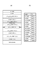
- the first and second contact layers are preferably made of gallium nitride. Since GaN is a gallium nitride-based semiconductor that is a binary compound, good crystal quality can be provided when the first and second contact layers are made of GaN.
- the carbon impurity concentration in the first contact layer is 1 ⁇ 10 17 cm ⁇ 3 or less.
- the contact resistance and the operating voltage of the device are improved.
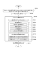
- the group III nitride semiconductor device 11 includes an electrode 41 (for example, a cathode).
- the electrode 41 is provided on the back surface 13b of the substrate 13 and is in direct contact with the back surface 13b.
- the electrode 41 is made of, for example, Pd, Ti / Al, or the like.
- TMG the supply of TMG is stopped and the substrate temperature is raised.
- TMG, NH 3 , Cp 2 Mg, and atmospheric gas are supplied to the growth furnace 10 to grow and form the p-type GaN electron block layer 65a at a substrate temperature of about 900 degrees Celsius.
- nitrogen it is preferable to supply nitrogen as an atmospheric gas.
- TMG, TMI, NH 3 , Cp 2 Mg and nitrogen are supplied to the growth reactor 10 to grow and form the Mg-doped InGaN optical guide layer 65b at a substrate temperature of about 840 degrees Celsius.
- a low-concentration Mg-doped GaN contact layer 65e (corresponding to the contact layer 25a) and a high-concentration Mg-doped GaN contact layer 65f (corresponding to the contact layer 25b) are grown and formed.
- TMG, NH 3 , Cp 2 Mg, and atmospheric gas are supplied to the growth reactor 10 at about 900 degrees Celsius to grow and form the low-concentration Mg-doped GaN contact layer 65e.
- the thickness of the low-concentration Mg-doped GaN contact layer 65e is about 40 nm.
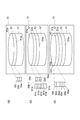
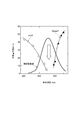
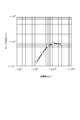
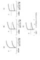
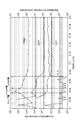
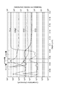
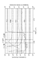
- FIGS. 13 to 15 show SIMS results obtained by analyzing the structure of the epitaxial stack from the surface side.
- the epitaxial laminated structure used in this analysis is a structure in which an undoped GaN cap layer is laminated on the high-concentration Mg-doped GaN contact layer 65f in order to accurately measure the atomic concentration of the contact layer.
- the horizontal axis of each figure shows the depth from the surface (p-side surface) of this epitaxial stack.
- the analysis results from the surface of the epitaxial stack (p-side surface) to about 200 nm are shown.
- the SIMS results shown in FIGS. 13 to 15 include analysis results for magnesium (Mg), aluminum (Al), and indium (In) as markers.
Landscapes
- Physics & Mathematics (AREA)
- Optics & Photonics (AREA)
- General Physics & Mathematics (AREA)
- Chemical & Material Sciences (AREA)
- Engineering & Computer Science (AREA)
- Nanotechnology (AREA)
- Condensed Matter Physics & Semiconductors (AREA)
- Electromagnetism (AREA)
- Biophysics (AREA)
- Crystallography & Structural Chemistry (AREA)
- Life Sciences & Earth Sciences (AREA)
- Led Devices (AREA)
- Semiconductor Lasers (AREA)
Priority Applications (3)
| Application Number | Priority Date | Filing Date | Title |
|---|---|---|---|
| EP12805410.3A EP2728683A1 (en) | 2011-06-29 | 2012-06-29 | Group iii nitride semiconductor element and method for manufacturing group iii nitride semiconductor element |
| KR1020137031086A KR20130141709A (ko) | 2011-06-29 | 2012-06-29 | Iii족 질화물 반도체 소자 및 iii족 질화물 반도체 소자의 제조 방법 |
| CN201280032130.2A CN103650263A (zh) | 2011-06-29 | 2012-06-29 | Iii族氮化物半导体元件及iii族氮化物半导体元件的制造方法 |
Applications Claiming Priority (4)
| Application Number | Priority Date | Filing Date | Title |
|---|---|---|---|
| JP2011-144664 | 2011-06-29 | ||
| JP2011144664 | 2011-06-29 | ||
| JP2012-111478 | 2012-05-15 | ||
| JP2012111478A JP2013033930A (ja) | 2011-06-29 | 2012-05-15 | Iii族窒化物半導体素子、及び、iii族窒化物半導体素子の製造方法 |
Publications (1)
| Publication Number | Publication Date |
|---|---|
| WO2013002389A1 true WO2013002389A1 (ja) | 2013-01-03 |
Family
ID=47424274
Family Applications (1)
| Application Number | Title | Priority Date | Filing Date |
|---|---|---|---|
| PCT/JP2012/066769 WO2013002389A1 (ja) | 2011-06-29 | 2012-06-29 | Iii族窒化物半導体素子、及び、iii族窒化物半導体素子の製造方法 |
Country Status (7)
Families Citing this family (15)
| Publication number | Priority date | Publication date | Assignee | Title |
|---|---|---|---|---|
| JP5781032B2 (ja) * | 2012-07-30 | 2015-09-16 | 株式会社東芝 | 半導体発光素子 |
| JP2015170803A (ja) * | 2014-03-10 | 2015-09-28 | 住友電気工業株式会社 | III族窒化物半導体素子、p型コンタクト構造、III族窒化物半導体素子を作製する方法 |
| JP6249868B2 (ja) * | 2014-04-18 | 2017-12-20 | サンケン電気株式会社 | 半導体基板及び半導体素子 |
| KR101636625B1 (ko) * | 2014-12-18 | 2016-07-05 | 고려대학교 산학협력단 | p형 반도체 박막 구조물의 형성 방법 및 이를 이용한 p형 오믹 전극의 제조 방법 |
| TWI581453B (zh) * | 2014-12-23 | 2017-05-01 | 錼創科技股份有限公司 | 半導體發光元件 |
| US20170207365A1 (en) * | 2016-01-20 | 2017-07-20 | Google Inc. | Layered active region light emitting diode |
| DE102017121484A1 (de) | 2017-06-21 | 2018-12-27 | Osram Opto Semiconductors Gmbh | Halbleiterkörper und Verfahren zur Herstellung eines Halbleiterkörpers |
| JP7043802B2 (ja) * | 2017-11-16 | 2022-03-30 | 住友電気工業株式会社 | 垂直共振型面発光レーザ、垂直共振型面発光レーザを作製する方法 |
| DE112019000483T5 (de) * | 2018-01-23 | 2020-10-29 | Sony Semiconductor Solutions Corporation | Halbleiterlaser und elektronische vorrichtung |
| JP6785455B2 (ja) * | 2018-05-11 | 2020-11-18 | パナソニックIpマネジメント株式会社 | 発光ダイオード素子、及び発光ダイオード素子の製造方法 |
| US11228160B2 (en) * | 2018-11-15 | 2022-01-18 | Sharp Kabushiki Kaisha | AlGaInPAs-based semiconductor laser device and method for producing same |
| JP7288936B2 (ja) * | 2021-09-21 | 2023-06-08 | 日機装株式会社 | 窒化物半導体発光素子 |
| CN114497304B (zh) * | 2022-01-28 | 2024-12-27 | 安徽格恩半导体有限公司 | 一种半导体元件 |
| CN114824019B (zh) * | 2022-04-08 | 2024-09-24 | 安徽格恩半导体有限公司 | 一种半导体发光元件 |
| WO2024257516A1 (ja) * | 2023-06-12 | 2024-12-19 | パナソニックホールディングス株式会社 | 窒化物半導体発光素子及び窒化物半導体発光素子の製造方法 |
Citations (5)
| Publication number | Priority date | Publication date | Assignee | Title |
|---|---|---|---|---|
| JPH0897471A (ja) | 1994-09-20 | 1996-04-12 | Toyoda Gosei Co Ltd | 3族窒化物半導体発光素子 |
| JP2003023179A (ja) * | 2001-07-06 | 2003-01-24 | Ricoh Co Ltd | p型III族窒化物半導体およびその作製方法および半導体装置およびその作製方法 |
| JP2010067953A (ja) * | 2009-06-29 | 2010-03-25 | Sumitomo Electric Ind Ltd | 窒化物系半導体光素子、窒化物系半導体光素子のためのエピタキシャルウエハ、及び半導体発光素子を製造する方法 |
| JP2010263176A (ja) * | 2008-08-04 | 2010-11-18 | Sumitomo Electric Ind Ltd | GaN系半導体光素子、GaN系半導体光素子を作製する方法、及びエピタキシャルウエハ |
| JP2011029244A (ja) * | 2009-07-21 | 2011-02-10 | Nec Corp | 半導体、半導体の製造方法、半導体素子、半導体発光素子、半導体素子または半導体発光素子の製造方法 |
Family Cites Families (16)
| Publication number | Priority date | Publication date | Assignee | Title |
|---|---|---|---|---|
| JPH10173227A (ja) * | 1996-12-06 | 1998-06-26 | Toyoda Gosei Co Ltd | GaN系素子 |
| JP2004214337A (ja) * | 2002-12-27 | 2004-07-29 | Nichia Chem Ind Ltd | 窒化物半導体発光素子 |
| JP2005203411A (ja) * | 2004-01-13 | 2005-07-28 | Matsushita Electric Ind Co Ltd | 窒化物半導体発光素子 |
| JP2006229008A (ja) * | 2005-02-18 | 2006-08-31 | Opnext Japan Inc | 半導体レーザ素子 |
| JP2007227832A (ja) * | 2006-02-27 | 2007-09-06 | Matsushita Electric Ind Co Ltd | 窒化物半導体素子 |
| JP2009071162A (ja) * | 2007-09-14 | 2009-04-02 | Rohm Co Ltd | 半導体装置及び半導体装置の製造方法 |
| JP4462330B2 (ja) * | 2007-11-02 | 2010-05-12 | 住友電気工業株式会社 | Iii族窒化物電子デバイス |
| US8569794B2 (en) * | 2008-03-13 | 2013-10-29 | Toyoda Gosei Co., Ltd. | Group III nitride semiconductor device and method for manufacturing the same, group III nitride semiconductor light-emitting device and method for manufacturing the same, and lamp |
| JP5218117B2 (ja) * | 2008-03-18 | 2013-06-26 | 三菱電機株式会社 | 窒化物半導体積層構造及び光半導体装置並びにその製造方法 |
| JP5334501B2 (ja) * | 2008-09-02 | 2013-11-06 | 日立電線株式会社 | 窒化物半導体素子 |
| KR101142672B1 (ko) * | 2008-09-11 | 2012-05-11 | 스미토모덴키고교가부시키가이샤 | 질화물계 반도체 광소자, 질화물계 반도체 광소자용의 에피택셜 웨이퍼, 및 반도체 발광 소자를 제조하는 방법 |
| JP5262533B2 (ja) * | 2008-09-30 | 2013-08-14 | 豊田合成株式会社 | 半導体装置の製造方法 |
| JP2011009610A (ja) * | 2009-06-29 | 2011-01-13 | Sharp Corp | 窒化物半導体レーザ素子及びウェハ |
| JP5381439B2 (ja) * | 2009-07-15 | 2014-01-08 | 住友電気工業株式会社 | Iii族窒化物半導体光素子 |
| JP5635246B2 (ja) * | 2009-07-15 | 2014-12-03 | 住友電気工業株式会社 | Iii族窒化物半導体光素子及びエピタキシャル基板 |
| JP5310382B2 (ja) * | 2009-08-24 | 2013-10-09 | 住友電気工業株式会社 | Iii族窒化物半導体光素子、及びiii族窒化物半導体光素子を作製する方法 |
-
2012
- 2012-05-15 JP JP2012111478A patent/JP2013033930A/ja active Pending
- 2012-06-29 CN CN201280032130.2A patent/CN103650263A/zh active Pending
- 2012-06-29 EP EP12805410.3A patent/EP2728683A1/en not_active Withdrawn
- 2012-06-29 TW TW101123757A patent/TW201310705A/zh unknown
- 2012-06-29 KR KR1020137031086A patent/KR20130141709A/ko not_active Ceased
- 2012-06-29 US US13/538,513 patent/US20130009202A1/en not_active Abandoned
- 2012-06-29 WO PCT/JP2012/066769 patent/WO2013002389A1/ja active Application Filing
Patent Citations (5)
| Publication number | Priority date | Publication date | Assignee | Title |
|---|---|---|---|---|
| JPH0897471A (ja) | 1994-09-20 | 1996-04-12 | Toyoda Gosei Co Ltd | 3族窒化物半導体発光素子 |
| JP2003023179A (ja) * | 2001-07-06 | 2003-01-24 | Ricoh Co Ltd | p型III族窒化物半導体およびその作製方法および半導体装置およびその作製方法 |
| JP2010263176A (ja) * | 2008-08-04 | 2010-11-18 | Sumitomo Electric Ind Ltd | GaN系半導体光素子、GaN系半導体光素子を作製する方法、及びエピタキシャルウエハ |
| JP2010067953A (ja) * | 2009-06-29 | 2010-03-25 | Sumitomo Electric Ind Ltd | 窒化物系半導体光素子、窒化物系半導体光素子のためのエピタキシャルウエハ、及び半導体発光素子を製造する方法 |
| JP2011029244A (ja) * | 2009-07-21 | 2011-02-10 | Nec Corp | 半導体、半導体の製造方法、半導体素子、半導体発光素子、半導体素子または半導体発光素子の製造方法 |
Non-Patent Citations (2)
| Title |
|---|
| JAPANESE JOURNAL OF APPLIED PHYSICS, vol. 39, 2000, pages 413 |
| JOURNAL OF APPLIED PHYSICS, vol. 91, no. 12, 2002, pages 9904 |
Also Published As
| Publication number | Publication date |
|---|---|
| EP2728683A1 (en) | 2014-05-07 |
| JP2013033930A (ja) | 2013-02-14 |
| US20130009202A1 (en) | 2013-01-10 |
| CN103650263A (zh) | 2014-03-19 |
| KR20130141709A (ko) | 2013-12-26 |
| TW201310705A (zh) | 2013-03-01 |
Similar Documents
| Publication | Publication Date | Title |
|---|---|---|
| WO2013002389A1 (ja) | Iii族窒化物半導体素子、及び、iii族窒化物半導体素子の製造方法 | |
| JP5003527B2 (ja) | Iii族窒化物発光素子、及びiii族窒化物系半導体発光素子を作製する方法 | |
| JP5306254B2 (ja) | 半導体発光素子 | |
| JP5316276B2 (ja) | 窒化物半導体発光素子、エピタキシャル基板、及び窒化物半導体発光素子を作製する方法 | |
| JP5842324B2 (ja) | Iii族窒化物半導体素子、iii族窒化物半導体素子を作製する方法、及びエピタキシャル基板 | |
| US8548021B2 (en) | III-nitride semiconductor laser, and method for fabricating III-nitride semiconductor laser | |
| CN102124578B (zh) | Ⅲ族氮化物半导体光元件 | |
| CN101958509B (zh) | 氮化镓类半导体激光二极管 | |
| US20110212560A1 (en) | Method for fabricating nitride semiconductor light emitting device and method for fabricating epitaxial wafer | |
| US20110042646A1 (en) | Nitride semiconductor wafer, nitride semiconductor chip, method of manufacture thereof, and semiconductor device | |
| CN101874309A (zh) | 氮化物类半导体光元件、用于氮化物类半导体光元件的外延晶片及制造半导体发光元件的方法 | |
| KR20100099066A (ko) | 질화갈륨계 반도체 광소자, 질화갈륨계 반도체 광소자를 제조하는 방법 및 에피택셜 웨이퍼 | |
| JP5326787B2 (ja) | Iii族窒化物半導体レーザダイオード、及びiii族窒化物半導体レーザダイオードを作製する方法 | |
| JP5651077B2 (ja) | 窒化ガリウム系半導体レーザ素子、及び、窒化ガリウム系半導体レーザ素子の製造方法 | |
| JP5522147B2 (ja) | 窒化物半導体発光素子、及び、窒化物半導体発光素子の作製方法 | |
| JP4788138B2 (ja) | 窒化物半導体素子 | |
| JP5012629B2 (ja) | 窒化物半導体素子の製造方法 | |
| WO2014088030A1 (ja) | 窒化物半導体発光素子、窒化物半導体発光素子を作製する方法 | |
| JP2012256948A (ja) | 半導体発光素子 | |
| JP2011188000A (ja) | Iii族窒化物半導体レーザ、及びiii族窒化物半導体レーザを作製する方法 | |
| JP2014078763A (ja) | 窒化物半導体発光素子、及び、窒化物半導体発光素子の作製方法 | |
| JP2012109624A (ja) | Iii族窒化物発光素子、及びiii族窒化物系半導体発光素子を作製する方法 | |
| JP2012044228A (ja) | Iii族窒化物半導体レーザ、及びiii族窒化物半導体レーザを作製する方法 |
Legal Events
| Date | Code | Title | Description |
|---|---|---|---|
| 121 | Ep: the epo has been informed by wipo that ep was designated in this application |
Ref document number: 12805410 Country of ref document: EP Kind code of ref document: A1 |
|
| ENP | Entry into the national phase |
Ref document number: 20137031086 Country of ref document: KR Kind code of ref document: A |
|
| NENP | Non-entry into the national phase |
Ref country code: DE |
|
| WWE | Wipo information: entry into national phase |
Ref document number: 2012805410 Country of ref document: EP |