WO2012176826A1 - インバータ装置 - Google Patents
インバータ装置 Download PDFInfo
- Publication number
- WO2012176826A1 WO2012176826A1 PCT/JP2012/065803 JP2012065803W WO2012176826A1 WO 2012176826 A1 WO2012176826 A1 WO 2012176826A1 JP 2012065803 W JP2012065803 W JP 2012065803W WO 2012176826 A1 WO2012176826 A1 WO 2012176826A1
- Authority
- WO
- WIPO (PCT)
- Prior art keywords
- phase
- frequency
- phase signal
- signal
- unit
- Prior art date
- Legal status (The legal status is an assumption and is not a legal conclusion. Google has not performed a legal analysis and makes no representation as to the accuracy of the status listed.)
- Ceased
Links
Images





Classifications
-
- H—ELECTRICITY
- H02—GENERATION; CONVERSION OR DISTRIBUTION OF ELECTRIC POWER
- H02M—APPARATUS FOR CONVERSION BETWEEN AC AND AC, BETWEEN AC AND DC, OR BETWEEN DC AND DC, AND FOR USE WITH MAINS OR SIMILAR POWER SUPPLY SYSTEMS; CONVERSION OF DC OR AC INPUT POWER INTO SURGE OUTPUT POWER; CONTROL OR REGULATION THEREOF
- H02M7/00—Conversion of AC power input into DC power output; Conversion of DC power input into AC power output
- H02M7/42—Conversion of DC power input into AC power output without possibility of reversal
- H02M7/44—Conversion of DC power input into AC power output without possibility of reversal by static converters
- H02M7/48—Conversion of DC power input into AC power output without possibility of reversal by static converters using discharge tubes with control electrode or semiconductor devices with control electrode
- H02M7/53—Conversion of DC power input into AC power output without possibility of reversal by static converters using discharge tubes with control electrode or semiconductor devices with control electrode using devices of a triode or transistor type requiring continuous application of a control signal
- H02M7/537—Conversion of DC power input into AC power output without possibility of reversal by static converters using discharge tubes with control electrode or semiconductor devices with control electrode using devices of a triode or transistor type requiring continuous application of a control signal using semiconductor devices only, e.g. single switched pulse inverters
- H02M7/5387—Conversion of DC power input into AC power output without possibility of reversal by static converters using discharge tubes with control electrode or semiconductor devices with control electrode using devices of a triode or transistor type requiring continuous application of a control signal using semiconductor devices only, e.g. single switched pulse inverters in a bridge configuration
- H02M7/53871—Conversion of DC power input into AC power output without possibility of reversal by static converters using discharge tubes with control electrode or semiconductor devices with control electrode using devices of a triode or transistor type requiring continuous application of a control signal using semiconductor devices only, e.g. single switched pulse inverters in a bridge configuration with automatic control of output voltage or current
- H02M7/53875—Conversion of DC power input into AC power output without possibility of reversal by static converters using discharge tubes with control electrode or semiconductor devices with control electrode using devices of a triode or transistor type requiring continuous application of a control signal using semiconductor devices only, e.g. single switched pulse inverters in a bridge configuration with automatic control of output voltage or current with analogue control of three-phase output
Definitions
- the present invention relates to an inverter device that converts DC power into AC power synchronized with the power system and superimposes the AC power on the power system.
- a technique for estimating a frequency shift (frequency change amount) from a reference frequency of an input AC single-phase signal is a technique necessary for a single-phase signal input device, for example, an inverter system.
- the inverter system converts, for example, DC power output from a DC power source such as a solar battery into AC power synchronized with the power system, and superimposes this AC power on the power system to supply the superimposed AC power to the load. It is.
- the output voltage signal of the inverter circuit connected to the power system is regarded as a single-phase signal, if the frequency deviation (frequency change amount) of the output voltage signal of the inverter circuit from the reference frequency can be detected, it is operated independently. Can be detected.
- Single operation refers to a state where only the inverter circuit of the power system and the inverter circuit supplies power to the load. Independent operation can occur when a power failure occurs on the power system side. For the purpose of ensuring safety or the like, when an isolated operation occurs, it is required to quickly detect this and stop the output of the inverter circuit. Therefore, speeding up or increasing the accuracy of frequency deviation detection that can be used for isolated operation detection is beneficial.
- a method for detecting the phase and frequency of a single-phase signal from the zero-cross timing of the single-phase signal is widely known. By using this method, it is possible to detect the frequency shift from the zero-cross timing of the single-phase signal.
- Patent Document 1 discloses a method of obtaining a complex vector (rotation vector) from a single-phase signal using Hilbert transform.
- Patent Documents 2 and 3 a signal having a phase difference of ⁇ / 2 with respect to a single-phase signal is generated using a filter in which an integral or differential characteristic is given to a bandpass filter, and a single-phase signal is generated using the generated signal.
- a method for estimating the phase of the signal is shown.
- JP 2003-143860 A JP 2006-129681 A JP 2008-141935 A
- the frequency can be detected only for each half cycle of the single-phase signal.
- the zero cross timing easily changes depending on noise and harmonic components included in the signal, the method using the zero cross timing is vulnerable to noise and harmonic components.
- the frequency deviation frequency change amount
- time for a plurality of periods of the single-phase signal is required to obtain substantially effective detection accuracy. Therefore, a method that can detect (including estimation) a frequency shift (frequency change amount) at higher speed or with higher accuracy is desired. Note that the methods disclosed in Patent Documents 1 to 3 cannot or are not sufficient for these demands.
- an object of the present invention is to provide an inverter device that contributes to good estimation of the frequency change amount of a single-phase signal with respect to a reference frequency.
- a first inverter device is an inverter device including an inverter circuit that converts DC power into AC power synchronized with a power system and superimposes the AC power on the power system.
- a voltage detection sensor for detecting a first single-phase signal indicating an AC voltage between the circuits, and using a reference frequency that is a reference value of the frequency of the output voltage of the power system, between the first single-phase signal and Generating a second single-phase signal having a predetermined phase difference from the first single-phase signal, and the first single-phase with respect to the reference frequency estimated based on the first single-phase signal and the second single-phase signal
- a phase adjustment of the estimated phase is performed based on the amount of change in the frequency of the signal and the estimated phase of the first single-phase signal estimated based on the first single-phase signal, and the estimated phase subjected to this phase adjustment Using DC And converting the AC power synchronized power to the power system.
- the frequency change amount may be estimated based on a product of the first and second single-phase signals.
- the reference frequency may be adjusted based on the estimated amount of change in the frequency, and the second single-phase signal may be generated using the adjusted reference frequency.
- Such adjustment of the reference frequency can contribute to improvement of the estimation accuracy of the frequency and phase of the single-phase signal.
- the reactive current component in the output alternating current of the power conversion circuit may be adjusted based on the amount of change in the frequency.
- Arbitrary phase characteristics can be realized with respect to the frequency of the single-phase signal by adjusting the reactive current component.
- the output of the inverter circuit may be stopped by detecting that the inverter circuit is operating alone.
- the 2nd inverter apparatus which concerns on this invention is provided with the inverter circuit which converts direct-current power into alternating current power synchronized with the electric power system, and superimposes this alternating current power on the said electric power system
- the single operation of the said inverter circuit is detected
- a voltage detection sensor for detecting a first single-phase signal indicating an AC voltage between the power system and the inverter circuit is provided, and a reference value of the frequency of the output voltage of the power system
- a second single-phase signal having a predetermined phase difference with the first single-phase signal is generated from the first single-phase signal, and the first single-phase signal and the second single-phase signal are used.
- a third inverter device is an inverter device including an inverter circuit that converts DC power into AC power synchronized with a power system and superimposes the AC power on the power system.
- a voltage detection sensor for detecting a first single-phase signal indicating an AC voltage between the circuits, and using a reference frequency that is a reference value of the frequency of the output voltage of the power system, between the first single-phase signal and A second single-phase signal having a predetermined phase difference is generated from the first single-phase signal, and the estimated phase of the first single-phase signal is estimated based on the first single-phase signal and the second single-phase signal. Is used to convert DC power into AC power synchronized with the power system.
- an inverter device that contributes to good estimation of the frequency change amount of a single-phase signal with respect to a reference frequency.
- FIG. 10 is a diagram illustrating a relationship between an ⁇ coordinate system and a PQ coordinate system according to the third embodiment.
- FIG. 4A is a diagram illustrating a waveform of each signal when the filter coefficient is not adjusted, and
- FIG. 5B is a diagram illustrating a waveform of each signal when the filter coefficient is adjusted.
- It is a block diagram of a single-phase signal input device according to the fourth embodiment. It is a block diagram of a single-phase signal input device according to the fifth embodiment.
- FIG. 4A is a diagram showing the waveform of each signal when phase adjustment is not performed
- FIG. 5B is a diagram showing the waveform of each signal when phase adjustment is performed.
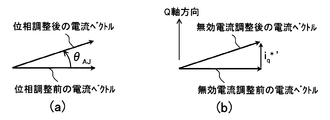
- FIG. 4A is a diagram for explaining the significance of phase adjustment
- FIG. 4B is a diagram for explaining the significance of reactive current adjustment.
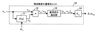
- FIG. 1 is an internal block diagram of a frequency variation estimation unit 10 (hereinafter sometimes abbreviated as estimation unit 10) according to the first embodiment of the present invention.
- the single-phase signal input device according to the first embodiment includes an estimation unit 10.
- the estimation unit 10 includes a filter 11, a multiplication unit 12, a DC component extraction unit 13, and a coefficient multiplication unit 14.
- Symbol v in is a single-phase signal of the AC input into a single-phase signal input device (the same is true in other embodiments described later).
- Type of physical quantity (voltage, current, speed, etc.) for single-phase signal v in is represented is arbitrary.
- Symbols v ⁇ and v ⁇ are also symbols representing AC single-phase signals. Unless otherwise described, the single-phase signal v ⁇ is the same as the single-phase signal v in.
- Filter 11 generates a signal v beta by performing filtering processing for delaying or advancing the phase of the filtered target signal to the signal v alpha as filtering target signal.
- the transfer function of the filter 11 is represented by F (s).
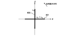
- FIG. 2 shows the ⁇ ⁇ coordinate system.
- the ⁇ ⁇ coordinate system is a two-dimensional fixed coordinate system having ⁇ and ⁇ axes as fixed axes as coordinate axes.
- the ⁇ and ⁇ axes are orthogonal to each other, and the ⁇ axis is advanced from the ⁇ axis by 90 degrees in electrical angle.
- the counterclockwise direction corresponds to the phase advance direction.
- solid line segments 601 and 602 represent the trajectories of signals v ⁇ and v ⁇ on the ⁇ coordinate system, respectively.
- the ⁇ axis is set so that the signal v ⁇ has only the ⁇ axis component.
- phase difference between the signal v beta and the signal v alpha is [pi / 2 (where, as will become apparent from the following description, the phase difference may shift from ⁇ / 2).
- a signal composed of two single-phase signals (for example, v ⁇ and v ⁇ ) can also be called a two-phase signal.
- ⁇ represents a circular ratio, and unless otherwise specified, the phase or angle is a phase or angle in electrical angle, and the unit of phase or angle expressed using ⁇ is radians.
- Reference frequency omega n is ignored the harmonic component corresponds to the angular frequency of the fundamental wave component in the signal v in.
- the reference frequency ⁇ n can be input not only to the single-phase signal input device but also to any part (including a unit, block, device, or system) described in this specification.
- filter 11 can perform filter processing using, for example, a transfer function F (s) represented by the following formula (A1) or (A2), and the signal v represented by formula (A3) is obtained by this filter processing.
- a signal v ⁇ represented by the equation (A4) is obtained from ⁇ .
- the operation symbol “s” represents a Laplace operator.
- “ ⁇ ” in the equation (A2) is a predetermined attenuation coefficient.
- V ⁇ and V ⁇ represent the amplitudes of the single-phase signals v ⁇ and v ⁇ , respectively.
- the symbol “t” represents time (more specifically, represents an elapsed time from a predetermined reference time when the signal value of the single-phase signal v ⁇ coincides with V ⁇ ).
- ⁇ is the frequency (angular frequency) of the single-phase signal v ⁇ .
- the DC component [v ⁇ ⁇ v ⁇ ] dc has a value corresponding to the frequency change amount ⁇ that is the change amount of the frequency ⁇ as viewed from the reference frequency ⁇ n .
- ⁇ ⁇ n .
- the direct current component [v ⁇ ⁇ v ⁇ ] dc is approximately proportional to the frequency change amount ⁇ . If the frequency change amount ⁇ is small with respect to the reference frequency ⁇ n (for example, sufficiently small), ⁇ is approximately proportional to ⁇ , and the DC component [v ⁇ ⁇ v ⁇ ] dc is also set to ⁇ as shown in the equation (A7). This is because it is roughly proportional.
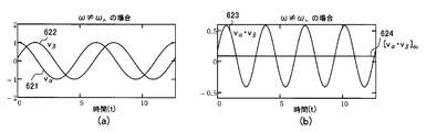
- FIG. 4 (a) shows the signal v alpha waveform 621 and the waveform 622 of the signal v beta when a ⁇ ⁇ ⁇ n, in FIG.
- the estimation unit 10 estimates the frequency change amount ⁇ using the above-described principle. That is, the multiplication unit 12 obtains a product (v ⁇ ⁇ v ⁇ ) of the single-phase signals v ⁇ and v ⁇ by multiplying the single-phase signals v ⁇ and v ⁇ .
- the DC component extraction unit 13 is, for example, a low-pass filter, and extracts a DC component [v ⁇ ⁇ v ⁇ ] dc by removing a frequency component of a predetermined frequency or higher from the product (v ⁇ ⁇ v ⁇ ).
- the frequency change amount ⁇ est may be obtained from the DC component [v ⁇ ⁇ v ⁇ ] dc .
- the DC component extraction unit 13 may obtain the DC component [v ⁇ ⁇ v ⁇ ] dc by obtaining a moving average of products (v ⁇ ⁇ v ⁇ ) for a plurality of periods, or may have a frequency of 2 ⁇ .
- the direct current component [v ⁇ ⁇ v ⁇ ] dc may be obtained by inputting the product (v ⁇ ⁇ v ⁇ ) to a band elimination filter that removes a nearby frequency.
- the direct current component extraction unit 13 may obtain the direct current component [v ⁇ ⁇ v ⁇ ] dc using a plurality of processes among the moving average process, the band removal process, and the high band removal process using the low pass filter.
- a signal having a phase difference of 90 degrees between the single-phase signal v alpha has been described above an example of obtaining a single-phase signal v beta, the phase difference between the single-phase signal v alpha and v beta is other than 90 degrees
- the single-phase signal v ⁇ may be obtained so that
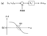
- the direct current component [v ⁇ ⁇ v ⁇ ] dc is set to a predetermined value, so that the direct current component as shown in FIG.
- the frequency change amount ⁇ est can be obtained.
- the predetermined value has a value corresponding to the phase difference between the single-phase signals v ⁇ and v ⁇ generated by the filter processing of the filter 11, and the phase difference between the single-phase signals v ⁇ and v ⁇ is 90 degrees. It is zero, but has a positive or negative value if the phase difference between the single phase signals v ⁇ and v ⁇ is other than 90 degrees.
- each part that performs a calculation operation uses the latest signal value obtained at each time point to perform the calculation itself.
- the value of the derivation target derived at an arbitrary part where the calculation operation is performed represents the instantaneous value of the derivation target.
- the value of the signal v beta filter 11 is derived at one time, the instantaneous value of the signal v beta at the time, [Delta] [omega est outputted by the estimation unit 10 at a certain time, the estimation of [Delta] [omega at the time Instantaneous value.
- ⁇ est derived by a later-described estimation unit 30 at a certain time is an estimated instantaneous value (estimated instantaneous phase) of ⁇ at the time.
- FIG. 6 is an internal block diagram of a frequency change amount estimation unit 20 (hereinafter sometimes abbreviated as estimation unit 20) according to the second embodiment of the present invention.
- the single-phase signal input device includes an estimation unit 20.
- the estimation unit 20 includes a filter 21, a multiplication unit 22, a DC component extraction unit 23, a PI control unit 24, and a subtraction unit 25.
- the estimation unit 20, a single-phase signal v in and the reference frequency omega n is input.
- the filter 21, the multiplication unit 22, and the DC component extraction unit 23 are the same as the filter 11, the multiplication unit 12, and the DC component extraction unit 13 of FIG. However, the filter 21 performs filter processing using the reference frequency omega n 'obtained by correcting the reference frequency omega n. Therefore, when using the transfer function F (s) of the formula (A1) or (A2), the filter 21 assigns “ ⁇ n ′” to “ ⁇ n ” of the formula (A1) or (A2). A single-phase signal v ⁇ is obtained.
- the DC component [v ⁇ ⁇ v ⁇ ] dc obtained by the DC component extraction unit 23 is sent to the PI control unit 24.
- a PLL Phase Locked Loop
- the PI control unit 24 uses the DC component [ v ⁇ ⁇ v ⁇ ]
- a value for converging dc to zero is output to the subtractor 25.
- Subtraction section 25 subtracts from the reference frequency omega n the output value of PI control unit 24 with respect to the subtraction section 25, it gives to the filter 21 the difference result as the reference frequency omega n '.
- the PI control unit 24 obtains an output value to the subtraction unit 25 so that the DC component [v ⁇ ⁇ v ⁇ ] dc becomes zero, that is, ( ⁇ n ′) becomes zero.
- the estimation unit 20 obtains the frequency change amount ⁇ est by multiplying the output value ( ⁇ ) of the PI control unit 24 by ( ⁇ 1).
- the estimation unit 20 adjusts the filter characteristics of the filter 21 based on the estimated frequency change amount ⁇ (that is, based on the output value of the PI control unit 24), and the subtraction unit 25 performs the adjustment.
- An adjustment part is formed.
- the amount to be adjusted is a filter coefficient ( ⁇ n ′) that determines the transfer function of the filter 21. Since the estimation unit 20 generates a two-phase signal (a two-phase signal composed of v ⁇ and v ⁇ ) adapted to the fluctuation of the frequency ⁇ , the estimation unit 20 can also be called a frequency tracking type two-phase signal generation unit. . Advantages of generating a two-phase signal adapted to fluctuations in the frequency ⁇ will be described in a third embodiment described later.
- the estimation unit 20 in FIG. 6 having a DC component functions [v ⁇ ⁇ v ⁇ ] where DC component and the DC component extraction unit 23 having a function of extracting a dc [v ⁇ ⁇ v ⁇ ] to converge dc to zero
- the PI control unit 24 is provided separately, but instead of the DC component extraction unit 23 and the PI control unit 24, an integrated control block (ie, a DC component [v ⁇ ⁇ v ⁇ A control block having a function of converging dc to zero (not shown) may be provided in the estimation unit 20.
- FIG. 3 shows an internal block diagram of a phase / frequency / frequency variation estimation unit 30 (hereinafter sometimes abbreviated as estimation unit 30) according to the third embodiment of the present invention.
- FIG. 3 further shows a two-phase signal generation unit 37 connected to the estimation unit 30.
- the single-phase signal input device according to the third embodiment includes an estimation unit 30 and a two-phase signal generation unit 37.
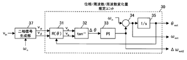
- the estimation unit 30 includes a coordinate rotation unit 31, a phase difference calculation unit 32, a PI control unit 33, an addition unit 34, and an integration unit 35.
- the PQ coordinate system and the like will be described with reference to FIG.
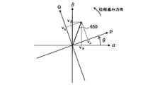
- FIG. 8 shows the relationship between the ⁇ coordinate system and the PQ coordinate system.
- the ⁇ coordinate system is a two-dimensional fixed coordinate system having ⁇ and ⁇ axes as fixed axes as coordinate axes.
- the PQ coordinate system is a two-dimensional rotation coordinate system having the rotation axes P and Q as coordinate axes.
- the P and Q axes are orthogonal to each other, and the Q axis is advanced from the P axis by an electrical angle of 90 degrees.
- the phase of the P axis viewed from the ⁇ axis is represented by ⁇ .
- ⁇ represents the advance angle of the phase of the P axis with respect to the ⁇ axis.
- reference numeral 650 represents a vector on an arbitrary coordinate system.
- Vector 650 represents the phase and amplitude state of any signal. Therefore, a signal whose phase and amplitude state are represented by the vector 650 can also be called a vector signal.
- the vector 650 is a vector that rotates in synchronization with the rotation of the PQ coordinate system. Then, since the vector 650 rotates on the ⁇ coordinate system, the vector 650 on the ⁇ coordinate system can also be called a rotation vector.
- the P-axis and Q-axis components of the vector 650 are represented by v p and v q, respectively.
- the ⁇ -axis and ⁇ -axis components of the vector 650 can be represented by v ⁇ and v ⁇ , respectively. It can be said that v ⁇ and v ⁇ are two orthogonal components (two components orthogonal to each other) of the rotation vector 650 on the ⁇ coordinate system, and v p and v q are two orthogonal components of the vector 650 on the PQ coordinate system. It can be said that.
- the frequency ⁇ of the single-phase signal v in it can be set to the angular frequency of the rotation of the PQ coordinate system. Therefore, the PQ coordinate system can be said to be a rotating coordinate system that rotates in synchronization with the frequency ⁇ .
- the phase ⁇ represents the phase of the single-phase signal vin (that is, “ ⁇ t” in the equation (A3)).
- the estimation unit 30 the estimated values of the phase ⁇ and the frequency ⁇ of the single-phase signal vin are obtained as ⁇ est and ⁇ est , respectively.
- the two-phase signal generating unit 37 using the method described in the first or second embodiment (see FIG. 1 or FIG. 6), a single-phase signal based on a single-phase signal v in and the reference frequency omega n A two-phase signal consisting of v ⁇ and v ⁇ is generated.
- the filter 11 may be provided in the two-phase signal generation unit 37.
- the estimation unit 20 may be provided in the two-phase signal generation unit 37.
- Single-phase signals v ⁇ and v ⁇ generated by the two-phase signal generation unit 37 are input to the coordinate rotation unit 31 of the estimation unit 30.
- the coordinate rotation unit 31 converts the signals v ⁇ and v ⁇ into signals v p and v q based on a phase ⁇ est output from the integration unit 35 described later. Since the vector 650 on the PQ coordinate system can be obtained by rotating the rotation vector 650 on the ⁇ coordinate system by the angle ⁇ , the coordinate rotation unit 31 performs the ⁇ coordinate system by coordinate conversion using ⁇ est as ⁇ .
- the orthogonal two components (v ⁇ and v ⁇ ) of the rotation vector 650 above can be converted to the orthogonal two components (v p and v q ) of the vector 650 on the PQ coordinate system.
- the phase difference calculation unit 32 obtains the phase difference ⁇ from v p and v q calculated by the coordinate rotation unit 31.
- Phase difference ⁇ represents the true phase theta of the single-phase signal v in, the error between the estimated value theta est phase theta.
- the estimation unit 30 makes ⁇ est coincide with ⁇ by configuring a PLL (Phase Locked Loop) according to the following equations (B2) and (B3) for converging ⁇ to zero.
- K P and K i are the proportional coefficient and integral coefficient of the proportional-integral control executed by the PI control unit 33, respectively.
- the PI control unit 33 and the addition unit 34 determine the frequency according to the equation (B2).
- ⁇ est is calculated.
- the integrator 35 calculates the phase ⁇ est by integrating the calculated frequency ⁇ est according to the equation (B3).
- the phase ⁇ est is sent to the coordinate rotation unit 31, and the coordinate rotation unit 31 performs coordinate conversion using ⁇ est as ⁇ .
- the phase theta est functions as an estimate of the phase theta of the single-phase signal v in.
- the frequency omega est which is the source of the theta est corresponds to the estimated value of the frequency omega of the single-phase signal v in.
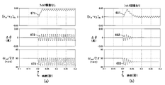
- Waveforms 671, 672, and 673 of FIG. 9A are respectively signal waveforms (time change of DC component [v ⁇ ⁇ v ⁇ ] dc , phase difference ⁇ , and frequency ⁇ est / 2 ⁇ obtained under the condition without adjustment. ), And the waveforms 681, 682, and 683 in FIG. 9B are signals having a DC component [v ⁇ ⁇ v ⁇ ] dc, a phase difference ⁇ , and a frequency ⁇ est / 2 ⁇ obtained under the adjusted condition, respectively. It represents a waveform (time change). Under the condition without adjustment, the filter 11 of FIG.
- FIG. 10 is a block diagram of a single-phase signal input device according to the fourth embodiment.
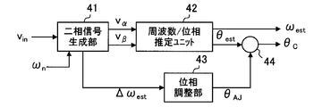
- the single-phase signal input device according to the fourth embodiment includes each part referred to by reference numerals 41 to 44.
- the two-phase signal generation unit 41 includes the estimation unit 10 of FIG. 1 or the estimation unit 20 of FIG. 6, and uses the method described in the first or second embodiment, and uses the single-phase signal v in and the reference frequency ⁇ n. Based on, a two-phase signal composed of single-phase signals v ⁇ and v ⁇ is generated and a frequency change amount ⁇ est is calculated.
- the frequency / phase estimation unit 42 (hereinafter sometimes abbreviated as the estimation unit 42) has the same configuration as the estimation unit 30 in FIG. 7, and the signals v ⁇ and v ⁇ from the two-phase signal generation unit 41 are used.
- phase adjustment unit 43 sets the phase adjustment amount ⁇ AJ based on the frequency change amount ⁇ est from the two-phase signal generation unit 41.
- the phase adjustment unit 43 sets the phase adjustment amount ⁇ AJ to zero when “
- ⁇ TH is a predetermined change amount threshold value having a positive value. However, ⁇ TH may be zero.
- the phase adjustment unit 43 can increase the absolute value of the phase adjustment amount ⁇ AJ as the absolute value
- phase adjustment portion such as the phase adjusting unit 43, corresponding to the frequency deviation of the single-phase signal v in to the reference frequency omega n, it is possible to form a phase estimator having an arbitrary phase characteristics ( The same applies to the fifth and sixth embodiments described later). The benefits of phase adjustment will be described in other embodiments described below.
- FIG. 11 is a block diagram of a single-phase signal input device according to the fifth embodiment.
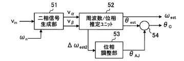
- the single-phase signal input device according to the fifth embodiment includes each part referred to by reference numerals 51 to 54.
- the two-phase signal generation unit 51 includes the estimation unit 10 in FIG. 1 or the estimation unit 20 in FIG. 6, and uses the method described in the first or second embodiment, and uses the single-phase signal v in and the reference frequency ⁇ n. To generate a two-phase signal composed of single-phase signals v ⁇ and v ⁇ .
- the frequency / phase estimation unit 52 (hereinafter sometimes abbreviated as the estimation unit 52) has the same configuration as that of the estimation unit 30 in FIG. 7, and uses the signals v ⁇ and v ⁇ from the two-phase signal generation unit 51. Based on this, the phase ⁇ est , the frequency ⁇ est, and the frequency change amount ⁇ est2 are calculated and output.
- the phase adjustment unit 53 sets the phase adjustment amount ⁇ AJ based on the frequency change amount ⁇ est2 from the estimation unit 52.
- the phase adjustment unit 53 sets the phase adjustment amount ⁇ AJ to zero when “
- the phase adjustment unit 53 can increase the absolute value of the phase adjustment amount ⁇ AJ as the absolute value
- FIG. 12 is a block diagram of a single-phase signal input device according to the sixth embodiment.
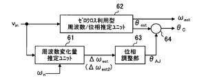
- the single-phase signal input device according to the sixth embodiment includes each part referred to by reference numerals 61 to 64.
- Frequency variation estimating unit 61 (hereinafter, sometimes abbreviated as estimation unit 61) is calculated and the frequency change [Delta] [omega est by estimating the frequency variation [Delta] [omega based on the single-phase signal v in and the reference frequency omega n Output.
- the estimation unit 61 may calculate the frequency change amount ⁇ est .
- the two-phase signal generation unit 37 and the estimation unit 30 of FIG. 7 may be provided in the estimation unit 61.
- ⁇ est2 output from the estimation unit 30 in the estimation unit 61 is set as ⁇ est from the estimation unit 61. Just output.
- Zero cross-using frequency / phase estimation unit 62 (hereinafter, sometimes abbreviated as estimation unit 62), (i.e., known zero-crossing by the signal value of the single-phase signal v in alternating detects the timing at which zero the timing detection method), obtains the phase theta and the estimated value in the form of the theta est and omega est frequency omega of the single-phase signal v in.
- the phase adjustment unit 63 sets the phase adjustment amount ⁇ AJ based on the frequency change amount ⁇ est from the estimation unit 61.
- the method of setting the phase adjustment amount ⁇ AJ in the phase adjustment unit 63 is the same as that in the phase adjustment unit 43 of FIG.
- the single-phase signal v in is assumed to be a voltage signal (i.e., signal representing a voltage value).
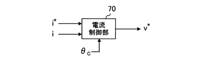
- the fourth, fifth or sixth phase obtained by the method shown in embodiment theta C i.e., may form a current control based on the phase theta C after adjustment. That is, a current control unit 70 as shown in FIG. 13 may be formed.
- the current control unit 70 calculates the voltage command value v * based on the current command value i *, the current value i, and the adjusted phase ⁇ C.
- the voltage command value v * corresponds to, for example, a voltage command value v S * in an eighth embodiment described later (see FIG. 14).
- the voltage command value v * represents, for example, a target value of the AC output voltage of the inverter circuit, and a single-phase signal v having a measured value of the AC output voltage itself or a value corresponding to the measured value as a signal value. it is in, it can be considered that.
- the current value i can be considered as an output current value of the inverter circuit, for example.
- the current command value i * is a target value of the current value i, and the current control unit 70 calculates the voltage command value v * so that the current error (i * ⁇ i) becomes zero.
- i * and i may be scalar quantities or vector quantities. A specific configuration example of the current control unit 70 will be described in an eighth embodiment described later.
- FIG. 14 is a schematic configuration diagram of an inverter system according to the eighth embodiment.
- the inverter system of FIG. 14 includes a solar battery 121 that is a DC power source, a single-phase inverter circuit 122, a control device 100 that controls the single-phase inverter circuit 122, and a power system 130 that outputs single-phase AC power. , Is provided.
- the control device 100 can also be called a power conversion control device or a power conversion control unit.
- the control device 100 is provided with each part referred to by reference numerals 101 to 107.
- a device including only the control device 100 or a device including the single-phase inverter circuit 122 and the control device 100 can be regarded as an inverter device.
- any part shown in FIG. 14 for example, the current detection sensor 125 and the voltage detection sensors 126 and 127) can also be regarded as being included in the components of the inverter device. It is.
- FIG. 14 shows an equivalent circuit of the solar cell 121.
- the solar cell 121 generates power based on solar energy and generates a DC voltage.
- DC voltage holding unit C d holds the DC voltage by storing charge corresponding to a DC voltage solar cell 121 occurs.
- the voltage detection sensor 127 detects the voltage value of the DC voltage E d held by the DC voltage holding unit C d, and sends a signal E d having the detected voltage value as a signal value to the DC voltage control unit 103.
- Single phase inverter circuit 122 having a plurality of switching elements by pulse width modulation using a switching operation of the switching elements, an AC voltage of the single-phase synchronous DC voltage from the DC voltage holding unit C d to the power grid 130 Convert.
- the AC voltage obtained by the single-phase inverter circuit 122 is output from the terminals 128 and 129 with the potential of the terminal 128 as a reference.
- the solar cell 121 may be disposed a booster circuit between the solar cell and single-phase inverter circuit 122.
- a filter circuit that removes harmonic components of the AC power output from the single-phase inverter circuit 122 is provided at the subsequent stage of the single-phase inverter circuit 122 (between the single-phase inverter circuit 122 and the current detection sensor 125). Usually placed.
- the electric power system 130 has an AC voltage source, and outputs (supplies) a single-phase AC voltage (for example, so-called commercial AC voltage) from the terminals 131 and 132 with the potential of the terminal 131 as a reference.
- a connection point 133 is provided on the wiring connecting the terminals 128 and 131 and a connection point 134 is provided on the wiring connecting the terminals 129 and 132, and an AC voltage between the connection points 133 and 134 is provided. Is connected between the interconnection points 133 and 134.
- the single-phase inverter circuit 122 converts DC power into AC power synchronized with the power system, and the AC power is superimposed on the power system and supplied to the load 135. That is, the load 135 is driven using the output AC power of the single-phase inverter circuit 122 and the output AC power of the power system 130.
- Lc represents the reactance component of the indoor wiring between the terminal 128 and the connection point 133 and the reactance component of the indoor wiring between the terminal 129 and the connection point 134
- Rc represents the resistance component of each of the indoor wirings.
- Ls represents the reactance component of the outdoor wiring connecting the terminal 131 and the interconnection point 133 and the reactance component of the outdoor wiring connecting the terminal 132 and the interconnection point 134
- Rs represents the resistance component of each outdoor wiring.
- the current detection sensor 125 detects the current value of the output current of the single-phase inverter circuit 122 and sends a signal i S having the detected current value as a signal value to the current control unit 104.
- the signal i S is not obtained by detecting the current between the terminal 128 and the interconnection point 133 (or between the terminal 129 and the interconnection point 134), but the current between the solar cell 121 and the single-phase inverter circuit 122 is obtained.
- the signal i S may be obtained by detection or by detecting the current in the single-phase inverter circuit 122.
- the voltage detection sensor 126 detects the voltage value of the output voltage of the single-phase inverter circuit 122 (that is, the voltage between the terminals 128 and 129 with reference to the potential of the terminal 128), and the signal v having the detected voltage value as a signal value. S is sent to a BPF (band pass filter) 101.
- the reference frequency ⁇ n is a frequency of the output voltage of the power system 130 (for example, a nominal frequency determined on the power system 130 side), and is, for example, 60 ⁇ 2 ⁇ or 50 ⁇ 2 ⁇ .
- BPF101 attenuates the harmonic components included in the signal v S (omega n higher-order components), and outputs the signal v S which has been made of this attenuation as the signal v S '.
- the symbols “i S ” and “v S ” are also used as symbols representing the output current and output voltage of the single-phase inverter circuit 122, respectively.
- the single phase signal input device of the fourth, fifth, or sixth embodiment can be included in the estimation / phase adjustment unit 102 (hereinafter may be abbreviated as the unit 102). That is, the unit 102 is provided with a single-phase signal input device having each part of FIG. 10, a single-phase signal input device having each part of FIG. 11, or a single-phase signal input device having each part of FIG. Can do.
- Unit 102 'receives as a single-phase signal v in, signals v S as a single-phase signal v in' signals v S from BPF101 and based on the reference frequency omega n, fourth, fifth or sixth embodiment
- the phase ⁇ C after adjustment, the frequency ⁇ est, and the frequency change amount ⁇ est are obtained according to the method described in.
- ⁇ est obtained by the unit 102 may be ⁇ est2 (see FIGS. 11 and 7).
- the phase ⁇ C derived by the unit 102 is sent to the current control unit 104, and ⁇ est or ⁇ est derived by the unit 102 is sent to the isolated operation detection unit 107.
- the DC voltage control unit 103 is given a DC voltage command value E d * in addition to the signal E d .
- DC voltage command value E d * from the solar cell 121 as the DC power source (in other words, the signal E d to maximize the output power of the single-phase inverter circuit 122) signal E d for obtaining a maximum power of Matches the value.
- the DC voltage control unit 103 calculates and outputs an effective current command value i p * using a proportional integral control or the like so that the value of the signal E d matches the command value E d * .
- the output current i S of the single-phase inverter circuit 122 is formed from an effective current and a reactive current (in other words, composed of an effective current component and a reactive current component).
- the effective current command value i p * corresponds to a target value of the effective current that forms the output current i S.
- the reactive current command value i q * shown later corresponds to the target value of the reactive current that forms the output current i S.
- the current control unit 104 uses the proportional integral control or the like to control the command value v SO *. Ask for.
- the current control unit 104 and the addition unit 105 handle the phase ⁇ C as the phase ⁇ , and generate command values v SO * and v S * for making the effective current component of the output current iS coincide with the command value i p *. To do.
- the PWM circuit 106 is configured so that the output voltage value of the single-phase inverter circuit 122 output from the BPF 101 (that is, the value of the signal v S ′) matches the voltage command value v S *. Control the switching element.
- the control device 100 through the control of the switching elements in accordance with the voltage command value v S *, realizes the control of the output AC current of the single-phase inverter circuit 122.
- the isolated operation detection unit 107 detects the isolated operation state of the single-phase inverter circuit 122 based on the frequency ⁇ est or the frequency change amount ⁇ est estimated by the unit 102 (in other words, whether or not an isolated operation has occurred). Detect).
- the single operation and the single operation state refer to a state in which only the single-phase inverter circuit 122 supplies power to the load 135. Independent operation can occur when a power failure occurs on the power system 130 side. For the purpose of ensuring safety or the like, when an isolated operation occurs, it is required to quickly detect this and stop the output of the single-phase inverter circuit 122. Therefore, when the detection unit 107 detects that an isolated operation is occurring, the control device 100 immediately stops the output of the inverter circuit 122.
- the isolated operation detection unit 107 compares the frequency ⁇ est with the reference frequency ⁇ n, and if the difference absolute value
- the isolated operation detection unit 107 compares the absolute value of ⁇ est with a predetermined threshold value TH B , and determines that an isolated operation has occurred if the absolute value of ⁇ est is greater than or equal to the threshold value TH B. If the absolute value of ⁇ est is less than the threshold value TH B , it may be determined that no isolated operation has occurred. TH B > 0.
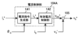
- FIG. 15 shows an internal block diagram of a current control unit 104A which is an example of the current control unit 104.
- the current control unit 104 ⁇ / b> A includes each part referred to by reference numerals 141 and 142.
- the current command generating unit 141 based on the phase theta C from unit 102, the phase theta C at after having handled as the phase theta, active current command value i p * of the output current command value i S from the DC voltage controller 103 Convert to * .
- the command value i S * is a sine wave current command value that functions as a target value for the output current i S of the interta 122.
- the effective current control unit 142 calculates the voltage command value v SO * using proportional-integral control or the like so that the output current value i S which is the value of the signal i S matches the command value i S * .
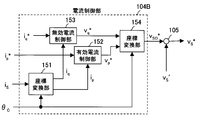
- FIG. 16 shows an internal block diagram of a current control unit 104B, which is another example of the current control unit 104.
- the current control unit 104B includes each part referred to by reference numerals 151 to 154.
- Coordinate conversion unit 151 based on the phase theta C from unit 102, in terms of dealing with phase theta C as the phase theta, coordinate transformation the output current of the inverter circuit 122 is represented by the signal i S to active current and reactive current Thus, the effective current value i p and the reactive current value i q are calculated.
- the coordinate conversion unit 151 has the same configuration as the two-phase signal generation unit 37 and the coordinate rotation unit 31 of FIG. That is, the coordinate conversion unit 151 is simply connected in the same manner as the two-phase voltage signals v p and v q are generated from the single-phase voltage signal vin in the two-phase signal generation unit 37 and the coordinate rotation unit 31.
- Two-phase current signals i p and i q are generated from the phase current signal iS.
- the output current i S can be considered to be the amount equivalent to the vector quantity, so that the output current i S output current It can also be called vector i S.
- the output current vector i S is a current vector on the PQ coordinate system.
- the active current control unit 152 is supplied with the active current command value i p * from the DC voltage control unit 103, and the reactive current control unit 153 is supplied with the reactive current command value i q * .
- Control device 100 can set zero to command value i q * .
- Active current controller 152 and the reactive current controller 153, respectively, the proportional integral control active current value i p and reactive current value i q or the like is the command value i p * and i q * and the voltage designated value v to match p * and v q * are calculated.
- Coordinate conversion unit 154 based on the phase theta C from unit 102, in terms of dealing with phase theta C as the phase theta, converts the voltage designated value v p * and v q * into voltage command values v SO *.
- the voltage command value v S * obtained using the coordinate conversion unit 154 and the addition unit 105 is expressed by Expression (C1).
- the estimation / phase adjustment unit 102 of FIG. 14 may be provided with the single-phase signal input device of FIG. 10, FIG. 11 or FIG.
- the process of generating the phase ⁇ C from the phase ⁇ est executed by the single-phase signal input device of FIG. 10, FIG. 11 or FIG. 12 is called phase adjustment. The significance of phase adjustment will be described.
- the frequency of the connection point voltage (voltage between the connection points 133 and 134) is the frequency of the output voltage of the power system 130 even if phase adjustment is performed. Therefore, the frequency of the voltages v S and v S ′ does not change from the frequency of the output voltage of the power system 130. However, if the voltage output from the power system 130 stops due to a power failure or the like, a voltage according to only the control of the control device 100 appears at the connection point and is detected by the voltage detection sensor 126.
- phase ⁇ of the voltage signal v S ′ advances.
- phase adjustment that is, ⁇ AJ > 0
- the phase of the connection point voltage advances via the phase change of the output current i S according to the phase adjustment, and the frequency of the connection point voltage is further increased. .
- the phase ⁇ of the voltage signal v S ′ is When the phase adjustment is performed so as to be delayed (that is, ⁇ AJ ⁇ 0), the phase of the connection point voltage is delayed through the phase change of the output current i S according to the phase adjustment, and the frequency of the connection point voltage is Further lower.
- the phase adjustment unit 43, 53, or 63 in the unit 102 is set so that the frequency of the connection point voltage increases or decreases. Is preferably formed (see FIG. 10, FIG. 11 or FIG. 12). That is, for example, the phase adjustment unit 43, 53, or 63 in the unit 102 sets the phase adjustment amount ⁇ AJ to zero when “
- the phase adjustment amount ⁇ AJ is set. It is better to set a negative value ( ⁇ TH ⁇ 0 as described in the fourth embodiment), and when “
- the absolute value of ⁇ AJ may be increased.
- ⁇ est2 is used as ⁇ est .
- the isolated operation detection unit 107 can detect whether or not an isolated operation has occurred based on the frequency ⁇ est or the frequency change amount ⁇ est estimated by the unit 102, and is necessary for the detection by phase adjustment. Time (the time required from when the isolated operation occurs until the isolated operation is detected) can be shortened. That is, the isolated operation detection can be speeded up.
- the inverter system of the ninth embodiment is different in that the estimation / phase adjustment unit 102 in the inverter system (FIG. 14) of the eighth embodiment operates as an estimation / phase adjustment unit 102A shown below.
- the estimation / phase adjustment unit 102A is the two-phase signal generation unit 41 and the frequency / phase estimation unit 42 in FIG. 10, or the two-phase signal generation unit 51 and the frequency / phase estimation unit 52 in FIG. 11, or the frequency in FIG. comprising a variation estimating unit 61 and the frequency / phase estimation unit 62, based on the voltage signal input v S 'and a single-phase signal v in the BPF101 to the reference frequency omega n, calculated theta est, omega est and [Delta] [omega est And output.
- ⁇ est2 is handled as ⁇ est .
- the current control unit 104 of the control device 100 performs the operation described in the eighth embodiment after using the estimated phase ⁇ est from the unit 102A as ⁇ C. Therefore, in the control device 100, the voltage command value v S * that is not affected by the phase adjustment is generated, and as a result, a current that is not affected by the phase adjustment is output from the single-phase inverter circuit 122.
- phase adjustment Even when phase adjustment is not performed, it is possible to detect an isolated operation in the same manner as when phase adjustment is performed. However, as can be understood from the effect of the phase adjustment, the detection speed of the isolated operation is faster when the phase adjustment is performed. Further, in a state where the output power of the inverter circuit 122 and the power consumption of the load 135 are balanced and no power is supplied from the power system 130 to the load 135 (hereinafter referred to as a balanced state), even if an isolated operation occurs, it is generally detected. However, if phase adjustment is performed, it is possible to reliably detect an isolated operation even in a balanced state.
- Waveforms 711, 712, and 713 in FIG. 17A are signal waveforms of the output voltage v S , the estimated frequency ⁇ est / 2 ⁇ , and the phase adjustment amount ⁇ AJ in the inverter system of the ninth embodiment that does not perform phase adjustment, respectively. (Time change). In the inverter system of the ninth embodiment, it can be considered that ⁇ AJ is always zero.
- FIGS. 17A and 17B are the signal waveforms (time) of the output voltage v S , the estimated frequency ⁇ est / 2 ⁇ , and the phase adjustment amount ⁇ AJ in the inverter system of the eighth embodiment that performs phase adjustment, respectively. Change).
- the estimated frequency ⁇ est quickly deviates from the reference frequency ⁇ n even in a balanced state. Can be detected.
- the current control unit 104C includes each part referred to by reference numerals 151 to 156.
- the reactive current adjustment unit 155 sets the reactive current adjustment amount i qAG based on ⁇ est estimated by the unit 102A of the ninth embodiment.
- the coordinate transformation unit 151 based on the phase theta est from unit 102A of the ninth embodiment, the output current i S active current and the phase theta est inverter circuit 122 on the handled as the phase theta decomposing the reactive current, thereby calculating the effective current value i p and reactive current value i q.
- the active current controller 152 and the reactive current controller 153 respectively, in proportion to the active current value i p and reactive current value i q matches the command value i p * and i q * 'integration using controls the calculated voltage designated value v p * and v q *, the coordinate transformation unit 154, based on the phase theta est from unit 102A of the ninth embodiment, after having handled the phase theta est as the phase theta
- the voltage designated values v p * and v q * are converted into voltage command values v SO * .
- the voltage command value v S * obtained using the coordinate conversion unit 154 and the addition unit 105 is expressed by Expression (D1).
- the phase corresponding to the frequency change amount ⁇ est is obtained as shown in FIG. 19A by using the adjusted phase ⁇ C for the calculation of the coordinate conversion units 151 and 154.
- the phase of the output current vector i S of the single-phase inverter circuit 122 is advanced (or delayed) by the adjustment amount ⁇ AJ .
- the current control unit 104C in FIG. 18 is used, as shown in FIG. 19B, the current command value i q * ′ corresponding to the frequency change amount ⁇ est is input to the reactive current control unit 153.
- the phase of the output current vector i S is advanced (or delayed). Therefore, also in the tenth embodiment (that is, even when the current control unit 104C is used), the same operation as that in the case of performing the phase adjustment of the eighth embodiment can be obtained, and the speed of isolated operation detection can be increased. It is done.
- the reactive current adjustment unit 155 sets the reactive current adjustment amount i qAG to zero when “
- qAG is set to a positive or negative value ( ⁇ TH ⁇ 0 as described in the fourth embodiment). More specifically, for example, the reactive current adjustment unit 155 sets a positive value for the adjustment amount i qAG when “
- the reactive current component of the output current i S is adjusted by the reactive current adjusting unit 155 and the adding unit 156 (in other words, the reactive current command value is adjusted), but the reactive current component is adjusted by the reactive power. Synonymous with adjustment.
- the frequency can be detected only for each half cycle of the single-phase signal.
- the zero cross timing easily changes depending on noise and harmonic components included in the signal, the method using the zero cross timing is vulnerable to noise and harmonic components.
- the frequency change amount ⁇ can be always estimated instead of every half cycle of the single-phase signal, so that the frequency ⁇ from the reference frequency ⁇ n can be estimated. Can be detected quickly. Further, since the fluctuation of the frequency ⁇ can be detected quickly, if the estimated value of the frequency change ⁇ by the single-phase input signal device is used for detection of the single operation (see FIG. 14), the single operation is performed using the zero cross timing. Single operation detection can be performed at a higher speed than when detection is performed.
- the filter coefficient ( ⁇ n ′) is adaptively adjusted based on the estimated value of the frequency change amount ⁇ , thereby improving the estimation accuracy of the frequency ⁇ and the phase ⁇ (FIG. 9).
- the phase of a single-phase signal may be estimated instantaneously and continuously, but the filter coefficient is fixed. Therefore, it cannot cope with frequency fluctuations.
- the filter coefficient of the two-phase signal generator is adjusted using the estimated frequency of the phase synchronizer, the phase synchronizer and the two-phase signal generator The design cannot be performed independently, and the design becomes complicated.
- phase adjustment based on the estimated value of the frequency change amount ⁇ is executed using the configuration shown in FIG. 10, FIG. 11 or FIG. 12, and current control is performed using the adjusted phase ⁇ C (FIG. 14, FIG. 15 and FIG. 16), an arbitrary phase characteristic can be realized with respect to the frequency ⁇ .
- the frequency ⁇ can be actively shifted from the reference frequency ⁇ n during the single operation. That is, since the frequency ⁇ can be shifted from the reference frequency ⁇ n in a short time after the occurrence of the isolated operation, the detection of the isolated operation can be speeded up.
- phase estimation and frequency change amount estimation can always be performed, so that high-speed frequency shift is possible (the frequency ⁇ is increased in a short time and the reference frequency ⁇ n is increased). Can be offset from).
- the estimation method can be used in combination with a method using zero-cross timing).
- the technique of the present invention is applied to a single-phase inverter device that performs system interconnection with a single-phase power system.
- the present invention includes the techniques of the above-described embodiments.
- the technology of the invention may be applied to a multi-phase inverter device (for example, a three-phase inverter device) that interconnects a multi-phase power system (for example, a three-phase power system).
- a single-phase signal v in is converted into a single-phase voltage (that is, a phase voltage or a line voltage) among a plurality of phase output voltages from a plurality of phase inverter circuits connected to a plurality of phase power systems.
- processing similar to that in each of the above-described embodiments may be performed.
- the method for deriving all the values to be derived is arbitrary. That is, for example, they may be derived by calculation, or may be derived from preset table data.
- Arbitrary portions for performing the arithmetic operation in each embodiment can be formed by software, hardware, or a combination of software and hardware.
- an arbitrary estimation unit can also be called an estimation unit or an estimation device (for example, a frequency change amount estimation unit can also be called a frequency change amount estimation unit), and a filter can be called a filter unit.
- the frequency variation estimating unit for estimating the frequency variation ⁇ on the basis of a single-phase signal v in, the phase estimator for estimating a phase ⁇ on the basis of a single-phase signal v in , and / or the frequency estimation unit for estimating the frequency ⁇ , based on the single-phase signal v in is inherent.
- the frequency change amount estimation unit corresponds to a part for obtaining the frequency change amount ⁇ est or ⁇ est2
- the phase estimation unit corresponds to a part for obtaining the phase ⁇ est
- the frequency estimation unit corresponds to a part for obtaining the frequency ⁇ est . Therefore, for example, the estimation unit 42, 52, or 62 (see FIG. 10, FIG. 11, or FIG. 12) includes a frequency change amount estimation unit, a phase estimation unit, and a frequency estimation unit, and the unit 102 or 102A (FIG. 14). Reference) also includes a frequency variation estimation unit, a phase estimation unit, and a frequency estimation unit.
Landscapes
- Engineering & Computer Science (AREA)
- Power Engineering (AREA)
- Control Of Electrical Variables (AREA)
- Supply And Distribution Of Alternating Current (AREA)
- Inverter Devices (AREA)
Abstract
【課題】基準周波数に対する単相信号の周波数変化量Δωを良好に推定する。 【解決手段】フィルタ11には、交流の単相信号vin(=vα)と、単相信号vinの周波数の基準値である基準周波数ωnとが入力される。フィルタ11は、単相信号vαに対するフィルタ処理によって、単相信号vαとの間で90度の位相差を有する単相信号vβを生成する。単相信号vα及びvβの積から直流成分[vα・vβ]dcを抽出し、直流成分[vα・vβ]dcに所定の係数を乗じることで周波数変化量Δωの推定値Δωestを算出する(Δω=ω-ωn)。
Description
本発明は、直流電力を電力系統に同期した交流電力に変換し、この交流電力を電力系統に重畳するインバータ装置に関する。
入力された交流の単相信号の、基準周波数からの周波数ずれ(周波数変化量)を推定する技術は、単相信号入力装置において必要な技術であり、例えばインバータシステムにおいて必要となる。インバータシステムは、例えば、太陽電池等の直流電源の出力する直流電力を電力系統に同期した交流電力に変換し、この交流電力を電力系統に重畳して負荷にこの重畳した交流電力を供給するものである。
インバータシステムにおいて、電力系統に接続されたインバータ回路の出力電圧信号を単相信号として捉えた場合、インバータ回路の出力電圧信号の、基準周波数からの周波数ずれ(周波数変化量)を検出できれば、単独運転の検出等を行うことができる。
インバータシステムにおいて、電力系統に接続されたインバータ回路の出力電圧信号を単相信号として捉えた場合、インバータ回路の出力電圧信号の、基準周波数からの周波数ずれ(周波数変化量)を検出できれば、単独運転の検出等を行うことができる。
単独運転とは、電力系統とインバータ回路のうちインバータ回路のみが負荷に電力を供給している状態を指す。単独運転は、電力系統側に停電が発生した場合に発生しうる。安全性確保等を目的として、単独運転の発生時には、速やかにこれを検知し、インバータ回路の出力を停止させることが求められる。故に、単独運転検出に利用可能な、周波数ずれの検出の高速化又は高精度化は有益である。
単相信号のゼロクロスタイミングから単相信号の位相や周波数を検出する方法が広く知られており、この方法を用いれば、単相信号のゼロクロスタイミングから上記周波数ずれを検出することが可能である。
尚、下記特許文献1には、ヒルベルト変換を用いて単相信号から複素ベクトル(回転ベクトル)を得る方法が示されている。また、下記特許文献2及び3には、バンドパスフィルタに積分又は微分特性を付与したフィルタを用いて単相信号との位相差がπ/2の信号を生成し、生成信号を用いて単相信号の位相を推定する方法が示されている。
上述のゼロクロスタイミングを利用する方法では、原理上、単相信号の半周期ごとしか周波数を検出することができない。また、信号に含まれるノイズや高調波成分によってゼロクロスタイミングが容易に変化するため、ゼロクロスタイミングを利用する方法は、ノイズや高調波成分に対して脆弱である。結果、ゼロクロスタイミングを利用して上記周波数ずれ(周波数変化量)を検出しようとした場合には、実質的に有効な検出精度を得るために単相信号の複数周期分の時間が必要になる。従って、周波数ずれ(周波数変化量)を、より高速に又は高精度に検出(推定を含む)できる方法が切望される。尚、特許文献1~3に示された方法は、これらの要望に対して対応できない或いは不十分である。
そこで本発明は、基準周波数に対する単相信号の周波数変化量の良好なる推定に寄与するインバータ装置を提供することを目的とする。
本発明に係る第1のインバータ装置は、直流電力を電力系統に同期した交流電力に変換し、該交流電力を前記電力系統に重畳するインバータ回路を備えたインバータ装置において、前記電力系統及前記インバータ回路間の交流電圧を示す第1単相信号を検出する電圧検出センサを備え、前記電力系統の出力電圧の周波数の基準値である基準周波数を用いて、前記第1単相信号との間で所定の位相差を有する第2単相信号を前記第1単相信号から生成し、前記第1単相信号及び前記第2単相信号に基づいて推定される前記基準周波数に対する前記第1単相信号の周波数の変化量と、前記第1単相信号に基づいて推定される前記第1単相信号の推定位相とに基づいて前記推定位相の位相調整を行い、この位相調整を行った推定位相を用いて直流電力を電力系統に同期した交流電力に変換することを特徴とする。
これにより、ゼロクロスタイミングを利用して周波数の変化量を求める方法と比べて、周波数の変化量を、より短時間で精度良く推定することが可能となる。また、推定位相の調整により、単相信号の周波数に対して任意の位相特性を実現することが可能となる。結果、単独運転時に能動的に周波数をシフトさせる制御を高速に行うことが可能となり、単独運転の高速検出につながる。
具体的には例えば、前記第1及び第2単相信号の積に基づき前記周波数の変化量を推定しても良い。
また例えば、推定した前記周波数の変化量に基づいて前記基準周波数を調整し、調整した基準周波数を用いて前記第2単相信号を生成しても良い。
このような基準周波数の調整は、単相信号の周波数や位相の推定精度向上に寄与しうる。
また例えば、前記周波数の変化量に基づき、前記電力変換回路の出力交流電流における無効電流成分を調整しても良い。
無効電流成分の調整により、単相信号の周波数に対して任意の位相特性を実現することが可能となる。
また例えば、前記周波数の変化量が所定の閾値よりも大きい場合、前記インバータ回路の単独運転が発生していると検出して前記インバータ回路の出力を停止しても良い。
本発明に係る第2のインバータ装置は、直流電力を電力系統に同期した交流電力に変換し、該交流電力を前記電力系統に重畳するインバータ回路を備え、前記インバータ回路の単独運転を検出した場合に前記インバータ回路を停止する前記インバータ装置において、前記電力系統及前記インバータ回路間の交流電圧を示す第1単相信号を検出する電圧検出センサを備え、前記電力系統の出力電圧の周波数の基準値である基準周波数を用いて、前記第1単相信号との間で所定の位相差を有する第2単相信号を前記第1単相信号から生成し、前記第1単相信号及び前記第2単相信号に基づいて推定される前記基準周波数に対する前記第1単相信号の周波数の変化量が所定の閾値よりも大きい場合、前記単独運転が発生していると検出することを特徴とする。
これにより、ゼロクロスタイミングを利用して周波数の変化量を求める方法と比べて、周波数の変化量を、より短時間で精度良く推定することが可能となる。また、この周波数の変化量を用いて単独運転の発生有無検出を行うようにすれば、ゼロクロスタイミングを利用して周波数の変化量を求める方法と比べて、より高速に単独運転の検出を行うことが可能となる。
本発明に係る第3のインバータ装置は、直流電力を電力系統に同期した交流電力に変換し、該交流電力を前記電力系統に重畳するインバータ回路を備えたインバータ装置において、前記電力系統及前記インバータ回路間の交流電圧を示す第1単相信号を検出する電圧検出センサを備え、前記電力系統の出力電圧の周波数の基準値である基準周波数を用いて、前記第1単相信号との間で所定の位相差を有する第2単相信号を前記第1単相信号から生成し、前記第1単相信号及び前記第2単相信号に基づいて推定される前記第1単相信号の推定位相を用いて直流電力を電力系統に同期した交流電力に変換する。
電力変換制御装置に上記の単相信号入力装置を設けておくことにより、ゼロクロスタイミングを利用して周波数の変化量を求める方法と比べて、周波数の変化量を、より短時間で精度良く推定することが可能となる。
本発明によれば、基準周波数に対する単相信号の周波数変化量の良好なる推定に寄与するインバータ装置を提供することが可能である。
以下、本発明の実施形態の例を、図面を参照して具体的に説明する。参照される各図において、同一の部分には同一の符号を付し、同一の部分に関する重複する説明を原則として省略する。尚、本明細書では、記述の簡略化上、情報、信号、物理量、状態量又は部材等を参照する記号又は符号を記すことによって該記号又は符号に対応する情報、信号、物理量、状態量又は部材等の名称を省略又は略記することがある。以下に、本発明に係る複数の実施形態を説明する。矛盾無き限り、複数の実施形態の内、或る実施形態に記載した事項を他の実施形態に適用することができ、複数の実施形態を組み合わせることも可能で
ある。
ある。
<<第1実施形態>>
本発明の第1実施形態を説明する。図1は、本発明の第1実施形態に係る周波数変化量推定ユニット10(以下、推定ユニット10と略記することがある)の内部ブロック図である。第1実施形態に係る単相信号入力装置は、推定ユニット10を備える。推定ユニット10は、フィルタ11、乗算部12、直流成分抽出部13及び係数乗算部14を備える。
本発明の第1実施形態を説明する。図1は、本発明の第1実施形態に係る周波数変化量推定ユニット10(以下、推定ユニット10と略記することがある)の内部ブロック図である。第1実施形態に係る単相信号入力装置は、推定ユニット10を備える。推定ユニット10は、フィルタ11、乗算部12、直流成分抽出部13及び係数乗算部14を備える。
記号vinは、単相信号入力装置に入力される交流の単相信号を表す(後述の他の実施形態においても同様)。単相信号vinが表す物理量(電圧、電流、速度など)の種類は任意である。記号vα及びvβも交流の単相信号を表す記号である。特に記述なき限り、単相信号vαは単相信号vinと同じものである。
フィルタ11は、フィルタリング対象信号の位相を遅らせる又は進ませるフィルタ処理をフィルタリング対象信号としての信号vαに施すことにより信号vβを生成する。フィルタ11の伝達関数はF(s)で表される。以下では、特に記述なき限り、フィルタ11において信号vαの位相を電気角で90度だけ遅らせる又は進ませるフィルタ処理が成されるものとする。従って、信号vβの位相は信号vαの位相よりも電気角で90度だけ遅れている或いは進んでいる。
図2に、αβ座標系を示す。αβ座標系は、固定軸であるα及びβ軸を座標軸とする二次元固定座標系である。α及びβ軸は互いに直交しており、β軸はα軸から電気角で90度だけ進んでいる。図2を含む任意の座標系を示す図において、反時計回り方向が位相の進み方向に対応する。図2において、実線線分601及び602は、それぞれαβ座標系上における信号vα及びvβの軌跡を表している。図2から分かるように、信号vαがα軸成分のみを持つようにα軸は設定される。信号vβと信号vαとの位相差はπ/2である(但し、後述の説明から明らかとなるように、該位相差はπ/2からずれうる)。2つの単相信号(例えば、vα及びvβ)から成る信号を二相信号と呼ぶこともできる。本明細書において、πは円周率を表し、特に記述なき限り、位相又は角度は電気角における位相又は角度であると共に、πを用いて表した位相又は角度の単位はラジアンである。
単相信号vinの周波数として単相信号入力装置に入力される既知の周波数を記号ωnにて表し、それを基準周波数と呼ぶ。基準周波数ωnは、高調波成分を無視した、信号vinの基本波成分の角周波数に相当する。尚、単相信号入力装置だけではなく、本明細書で述べる任意の部位(ユニット、ブロック、装置又はシステムを含む)に対して基準周波数ωnを入力することができる。
フィルタ11において信号vαの位相を電気角で90度だけ遅らせる又は進ませるフィルタ処理が成されると述べたが、フィルタ11は、基準周波数ωnが単相信号vinの周波数と一致するとみなしてフィルタ処理を行うため、単相信号vinの周波数が基準周波数ωnとずれている場合、信号vα及びvβの位相差はπ/2からΔφだけずれる。フィルタ11は、例えば下記式(A1)又は(A2)にて示される伝達関数F(s)を用いてフィルタ処理を成すことができ、このフィルタ処理によって、式(A3)にて示される信号vαから式(A4)にて示される信号vβが得られる。
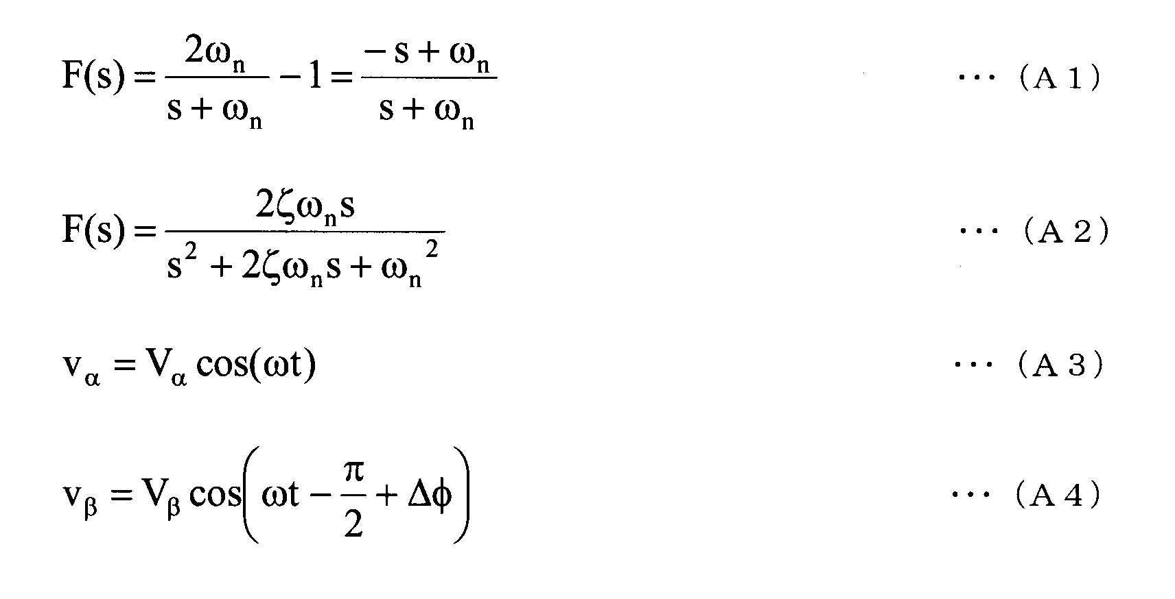
式(A1)及び(A2)並びに後述の式(B2)及び(B3)において、演算記号“s”はラプラス演算子を表す。式(A2)における“ζ”は所定の減衰係数である。Vα及びVβは、夫々、単相信号vα及びvβの振幅を表す。記号“t”は時間を表す(より詳細には、単相信号vαの信号値がVαと一致する所定の基準時刻からの経過時間を表す)。ωは、単相信号vαの周波数(角周波数)である。ω=ωnである場合、Δφはゼロであるが、ω≠ωnである場合、Δφは正又は負の角度値を有する。式(A4)に示される信号vβの位相(ωt-π/2+Δφ)は、式(A3)に示される信号vαの位相(ωt)よりも角度(π/2-Δφ)だけ遅れている。
式(A3)及び(A4)にて示される単相信号vα及びvβの積(vα・vβ)は、下記式(5)にて表され、積(vα・vβ)の直流成分を記号[vα・vβ]dcにて表すと、式(A5)から直流成分[vα・vβ]dcは式(A6)を満たす。更に、角度Δφが十分に小さいと仮定して式(A6)を近似すると式(A7)が得られる。

従って、単相信号vαの周波数ωが基準周波数ωnと一致する場合、Δφはゼロになるため直流成分[vα・vβ]dcはゼロになるが、単相信号vαの周波数ωが基準周波数ωnからずれると、フィルタ11の位相特性に起因して単相信号vα及びvβ間の位相差が90度からずれてΔφ≠0となり、結果、直流成分[vα・vβ]dcはゼロにならない。このように、直流成分[vα・vβ]dcは、基準周波数ωnから見た周波数ωの変化量である周波数変化量Δωに応じた値を持つ。Δω=ω-ωn、である。
周波数変化量Δωが基準周波数ωnに対して小さければ(例えば十分に小さければ)、直流成分[vα・vβ]dcは概ね周波数変化量Δωに比例する。周波数変化量Δωが基準周波数ωnに対して小さければ(例えば十分に小さければ)、ΔωはΔφに概ね比例し、式(A7)に示す如く直流成分[vα・vβ]dcもΔφに概ね比例するからである。従って、単相信号vα及びvβの積(vα・vβ)から直流成分[vα・vβ]dcを抽出し、抽出値に所定の係数を乗じれば周波数変化量Δωが得られる。
図3(a)に、ω=ωnである場合における信号vαの波形611及び信号vβの波形612を示し、図3(b)に、ω=ωnである場合における積(vα・vβ)の信号波形613及び直流成分[vα・vβ]dcの信号波形614を示す。図4(a)に、ω≠ωnである場合における信号vαの波形621及び信号vβの波形622を示し、図4(b)に、ω≠ωnである場合における積(vα・vβ)の信号波形623及び直流成分[vα・vβ]dcの信号波形624を示す。これらの信号波形からも、ω=ωnである場合には[vα・vβ]dc=0となる一方で、ω≠ωnである場合には[vα・vβ]dc≠0となることが分かる。
推定ユニット10では、上述の原理を利用して周波数変化量Δωを推定する。即ち、乗算部12は、単相信号vα及びvβを掛け合わせることで単相信号vα及びvβの積(vα・vβ)を求める。直流成分抽出部13は、例えばローパスフィルタであり、積(vα・vβ)から所定周波数以上の周波数成分を除去することで直流成分[vα・vβ]dcを抽出する。係数乗算部14は、直流成分[vα・vβ]dcに所定の係数Kωを乗じることで周波数変化量Δωestを求める(Δωest=[vα・vβ]dc×Kω)。周波数変化量Δωestを求めることは周波数変化量Δωを推定することに相当する。つまり、周波数変化量Δωestは周波数変化量Δωの推定値に相当し、推定誤差を無視すれば“Δωest=Δω”である。
尚、推定ユニット10において、直流成分[vα・vβ]dcと周波数変化量Δωestとの関係を定めるテーブルデータを予め用意しておき、係数乗算部14を用いる代わりに該テーブルデータを用いて直流成分[vα・vβ]dcから周波数変化量Δωestを求めるようにしても良い。また、直流成分抽出部13は、複数周期分の積(vα・vβ)の移動平均を求めることによって直流成分[vα・vβ]dcを求めても良いし、或いは、2ωの周波数近辺の周波数を除去する帯域除去フィルタに積(vα・vβ)を入力することによって直流成分[vα・vβ]dcを求めても良い。直流成分抽出部13は、移動平均処理及び帯域除去処理並びにローパスフィルタによる高域除去処理の内の複数の処理を用いて、直流成分[vα・vβ]dcを求めても良い。
また、単相信号vαとの間で90度の位相差を有する信号を単相信号vβとして求める例を上述したが、単相信号vα及びvβ間の位相差が90度以外になるように単相信号vβを求めても良い。即ち、ω=ωnであるときに単相信号vα及びvβ間の位相差が90度以外になるようなフィルタ処理をフィルタ11にて行うようにしても良い。この場合においても、式(A6)に示すのと同様にω=ωnであるならば直流成分[vα・vβ]dcは所定値に定まるため、図5(a)に示す如く直流成分[vα・vβ]dcから該所定値を差し引いて得た差分値に所定の係数Kω’を乗じることで(或いは該差分値に所定のテーブルデータを適用することで)、周波数変化量Δωestを求めることができる。上記所定値は、フィルタ11のフィルタ処理によって生じる単相信号vα及びvβ間の位相差に応じた値を持ち、単相信号vα及びvβ間の位相差が90度であるならばゼロであるが、単相信号vα及びvβ間の位相差が90度以外であるならば正又は負の値を持つ。
但し、上記所定値がゼロである場合に演算が最も簡素化されるため、単相信号vα及びvβ間の位相差が90度になるようにフィルタ処理を成すことが望ましい。更に、該位相差が90度であるとき、図5(b)に示される、ω及びΔφ間の関係の線形部分631を用いることができるため、制御にとって最も都合が良い。
尚、本実施形態及び後述の他の実施形態において、演算動作(フィルタ処理等をも含む)を行う各部位は、各時点で得られている最新の信号の値を用いて自身が成すべき演算を行い、所定の更新周期で自身が算出して出力すべき信号の値を更新する。従って、演算動作を行う任意の部位にて導出される導出対象の値は、その導出対象の瞬時値を表している。例えば、或る時刻においてフィルタ11が導出する信号vβの値は、当該時刻における信号vβの瞬時値であり、或る時刻において推定ユニット10が出力するΔωestは、当該時刻におけるΔωの推定瞬時値である。同様に例えば、後述の推定ユニット30(図7参照)が或る時刻において導出するθestは、当該時刻におけるθの推定瞬時値(推定された瞬時位相)である。
<<第2実施形態>>
本発明の第2実施形態を説明する。図6は、本発明の第2実施形態に係る周波数変化量推定ユニット20(以下、推定ユニット20と略記することがある)の内部ブロック図である。第2実施形態に係る単相信号入力装置は、推定ユニット20を備える。推定ユニット20は、フィルタ21、乗算部22、直流成分抽出部23、PI制御部24及び減算部25を備える。推定ユニット20には、単相信号vin及び基準周波数ωnが入力される。
本発明の第2実施形態を説明する。図6は、本発明の第2実施形態に係る周波数変化量推定ユニット20(以下、推定ユニット20と略記することがある)の内部ブロック図である。第2実施形態に係る単相信号入力装置は、推定ユニット20を備える。推定ユニット20は、フィルタ21、乗算部22、直流成分抽出部23、PI制御部24及び減算部25を備える。推定ユニット20には、単相信号vin及び基準周波数ωnが入力される。
フィルタ21、乗算部22及び直流成分抽出部23は、夫々、図1のフィルタ11、乗算部12及び直流成分抽出部13と同じものである。但し、フィルタ21は、基準周波数ωnを修正することで得た基準周波数ωn’を用いてフィルタ処理を行う。従って、式(A1)又は(A2)の伝達関数F(s)を利用する場合、フィルタ21は、式(A1)又は(A2)の「ωn」に「ωn’」を代入した上で単相信号vβを求める。
直流成分抽出部23にて求められた直流成分[vα・vβ]dcはPI制御部24に送られる。推定ユニット20では、直流成分[vα・vβ]dcをゼロに収束させるためのPLL(Phase Locked Loop)が形成されており、PI制御部24は、比例積分制御などを用いて直流成分[vα・vβ]dcをゼロに収束させるための値を減算部25に出力する。減算部25は、減算部25に対するPI制御部24の出力値を基準周波数ωnから差し引き、その差分結果を基準周波数ωn’としてフィルタ21に与える。
PI制御部24は、直流成分[vα・vβ]dcがゼロになるように、即ち(ω-ωn’)がゼロになるように減算部25への出力値を求めている。減算部25の機能を表す式「(ωn-(PI制御部24の出力値)=ωn’」に対し、PI制御部24の機能を表す式「ω-ωn’=0」を代入すると、PI制御部24の出力値は“ωn-ω”である。即ち、PI制御部24の出力値は周波数変化量Δω(=ω-ωn)に(-1)を乗じたものに相当する。推定ユニット20では、PI制御部24の出力値(-Δω)に対して(-1)を乗じることで周波数変化量Δωestを求める。
このように、推定ユニット20では、推定された周波数変化量Δωに基づき(即ちPI制御部24の出力値に基づき)フィルタ21のフィルタ特性が調整されており、減算部25が該調整を担うフィルタ調整部を形成する。調整の対象量は、フィルタ21の伝達関数を定めるフィルタ係数(ωn’)である。推定ユニット20では、周波数ωの変動に適応した二相信号(vα及びvβから成る二相信号)が生成されるため、推定ユニット20を周波数追従型二相信号生成部と呼ぶこともできる。周波数ωの変動に適応した二相信号を生成することの利点については、後述の第3実施形態の中で説明される。
尚、図6の推定ユニット20では、直流成分[vα・vβ]dcを抽出する機能を持つ直流成分抽出部23と直流成分[vα・vβ]dcをゼロに収束させる機能を持つPI制御部24とが別々に設けられているが、直流成分抽出部23及びPI制御部24の代わりに、それらの機能をまとめて有する一体の制御ブロック(即ち、直流成分[vα・vβ]dcをゼロに収束させる機能を持つ制御ブロック;不図示)を推定ユニット20に設けるようにしても良い。
<<第3実施形態>>
本発明の第3実施形態を説明する。図3には、本発明の第3実施形態に係る位相/周波数/周波数変化量推定ユニット30(以下、推定ユニット30と略記することがある)の内部ブロック図が示されている。図3には、更に、推定ユニット30に接続された二相信号生成部37が示されている。第3実施形態に係る単相信号入力装置は、推定ユニット30及び二相信号生成部37を備える。推定ユニット30は、座標回転部31、位相差算出部32、PI制御部33、加算部34及び積分部35を備える。推定ユニット30の動作を説明するに先立ち、図8を参照してPQ座標系等を説明する。
本発明の第3実施形態を説明する。図3には、本発明の第3実施形態に係る位相/周波数/周波数変化量推定ユニット30(以下、推定ユニット30と略記することがある)の内部ブロック図が示されている。図3には、更に、推定ユニット30に接続された二相信号生成部37が示されている。第3実施形態に係る単相信号入力装置は、推定ユニット30及び二相信号生成部37を備える。推定ユニット30は、座標回転部31、位相差算出部32、PI制御部33、加算部34及び積分部35を備える。推定ユニット30の動作を説明するに先立ち、図8を参照してPQ座標系等を説明する。
図8には、αβ座標系とPQ座標系との関係が示されている。上述したように、αβ座標系は、固定軸であるα及びβ軸を座標軸とする二次元固定座標系である。一方、PQ座標系は、回転軸であるP及びQ軸を座標軸とする二次元回転座標系である。P及びQ軸は互いに直交しており、Q軸はP軸から電気角で90度だけ進んでいる。α軸から見たP軸の位相をθにて表す。θは、α軸を基準とするP軸の位相の進み角度を表している。
図8において、符号650は任意の座標系上のベクトルを表している。ベクトル650は、任意の信号の位相及び振幅状態を表している。従って、ベクトル650によって位相及び振幅状態が表される信号を、ベクトル信号と呼ぶこともできる。今、ベクトル650が、PQ座標系の回転に同期して回転するベクトルであるとする。そうすると、αβ座標系上においてベクトル650は回転するため、αβ座標系上におけるベクトル650は回転ベクトルとも呼べる。ベクトル650のP軸及びQ軸成分を夫々vp及びvqにて表す。更に、ベクトル650のα軸及びβ軸成分を夫々vα及びvβにて表すことができる。vα及びvβは、αβ座標系上における回転ベクトル650の直交2成分(互いに直交する2つの成分)であると言え、vp及びvqは、PQ座標系上におけるベクトル650の直交2成分であると言える。
本明細書で述べる任意の部位(ユニット、ブロック、装置又はシステムを含む)において、単相信号vinの周波数ωをPQ座標系の回転における角周波数に設定することができる。従って、PQ座標系は周波数ωと同期して回転する回転座標系と言える。位相θは、単相信号vinの位相(即ち、式(A3)における“ωt”)を表している。推定ユニット30では、単相信号vinの位相θ及び周波数ωの推定値が、夫々、θest及びωestとして求められる。
図7において、二相信号生成部37は、第1又は第2実施形態で述べた方法を用いて(図1又は図6参照)、単相信号vin及び基準周波数ωnに基づき単相信号vα及びvβから成る二相信号を生成する。図1の構成を二相信号生成部37に適用する場合には、フィルタ11を二相信号生成部37に設けておけばよい。図6の構成を二相信号生成部37に適用する場合には、推定ユニット20を二相信号生成部37に設けておけばよい。
二相信号生成部37にて生成された単相信号vα及びvβは、推定ユニット30の座標回転部31に入力される。座標回転部31は、後述の積分部35から出力される位相θestに基づき信号vα及びvβを信号vp及びvqに変換する。αβ座標系上の回転ベクトル650を角度θだけ回転させることでPQ座標系上のベクトル650を得ることができるため、座標回転部31は、θestをθとして用いた座標変換によって、αβ座標系上の回転ベクトル650の直交2成分(vα及びvβ)を、PQ座標系上のベクトル650の直交2成分(vp及びvq)に変換することができる。
位相差算出部32は、座標回転部31にて算出されたvp及びvqから位相差Δθを求める。位相差Δθは、単相信号vinの真の位相θと、位相θの推定値θestとの間の誤差を表している。位相差算出部32は、下記式(B1)を用いて位相差Δθを求めることができる。座標回転部31における座標変換演算において、“θ=θest”を満たす推定値θestを用いたならば式(B1)の右辺の値はゼロになるが、“θ≠θest”を満たす推定値θestを用いたならば式(B1)の右辺の値はゼロにならない。

推定ユニット30では、Δθをゼロに収束させるための下記式(B2)及び(B3)に従うPLL(Phase Locked Loop)を構成することによってθestをθに一致させる。KP及びKiは、夫々、PI制御部33にて実行される比例積分制御の比例係数及び積分係数である。
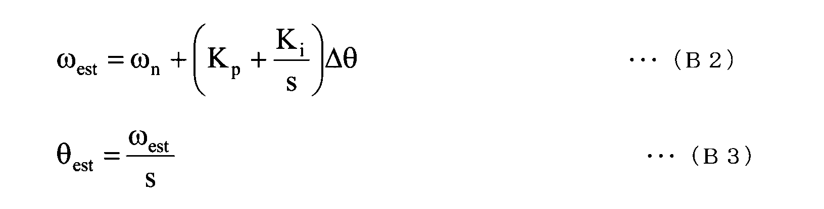
具体的には、位相差算出部32にて算出されたΔθと既知の角周波数として与えられた基準周波数ωnとに基づき、PI制御部33及び加算部34にて、式(B2)に従い周波数ωestを算出する。積分部35は、式(B3)に従い、算出された周波数ωestを積分することで位相θestを算出する。位相θestは座標回転部31に送られ、座標回転部31はθestをθとして用いて座標変換を行う。推定ユニット30では、位相差Δθがゼロに収束するようにPLLが構成されているため、位相θestは、単相信号vinの位相θの推定値として機能する。従って、θestの元となる周波数ωestは、単相信号vinの周波数ωの推定値に相当する。また、PI制御部33の出力値に相当する、式(B2)の右辺第2項は、式(B2)及び上述の関係式“Δω=ω-ωn”から分かるように、Δωの推定値として機能する。故に、PI制御部33から、Δωの推定値である周波数変化量Δωest2が出力される。推定誤差を無視すれば、Δω=Δωest2、である。
次に、図9(a)及び(b)を参照して、第2実施形態で述べたフィルタ特性の調整の作用について説明する。図9(a)の波形671、672、673は、それぞれ、調整なし条件下で得られた直流成分[vα・vβ]dc、位相差Δθ、周波数ωest/2πの信号波形(時間変化)を表し、図9(b)の波形681、682、683は、それぞれ、調整あり条件下で得られた直流成分[vα・vβ]dc、位相差Δθ、周波数ωest/2πの信号波形(時間変化)を表している。調整なし条件下では、図1のフィルタ11を用いて図7の二相信号生成部37を形成した上で、[vα・vβ]dc、Δθ及びωest/2πを求めた。調整あり条件下では、図6の推定ユニット20を用いて図7の二相信号生成部37を形成した上で、[vα・vβ]dc、Δθ及びωest/2πを求めた。
調整なし条件及び調整あり条件の夫々のシミュレーションにおいて、周波数ωn/2πを50Hz(ヘルツ)に固定し、特定のタイミングt0に単相信号vinの周波数ω/2πを50Hzから46Hzに急変させた。単相信号vinの周波数が変化したことによって信号vβの位相が変化し、これに伴ってΔθが大きく変動すると共に推定周波数ωestの変動も大きくなる。但し、図9(a)と図9(b)の対比から分かるように、第2実施形態の如くフィルタ特性を調整すると、単相信号vinの周波数変化後の推定周波数ωestの変動が改善される(変動が小さく抑えられる)。
<<第4実施形態>>
本発明の第4実施形態を説明する。図10は、第4実施形態に係る単相信号入力装置のブロック図である。第4実施形態に係る単相信号入力装置は、符号41~44によって参照される各部位を備える。
本発明の第4実施形態を説明する。図10は、第4実施形態に係る単相信号入力装置のブロック図である。第4実施形態に係る単相信号入力装置は、符号41~44によって参照される各部位を備える。
二相信号生成部41は、図1の推定ユニット10又は図6の推定ユニット20を有し、第1又は第2実施形態で述べた方法を用いて、単相信号vin及び基準周波数ωnに基づき単相信号vα及びvβから成る二相信号を生成すると共に周波数変化量Δωestを算出する。周波数/位相推定ユニット42(以下、推定ユニット42と略記することがある)は、図7の推定ユニット30と同様の構成を有し、二相信号生成部41からの信号vα及びvβに基づき単相信号vinの位相θ及び周波数ωを推定することにより、推定位相θest及び推定周波数ωestを算出及び出力する。位相調整部43は、二相信号生成部41からの周波数変化量Δωestに基づき位相調整量θAJを設定する。加算部44は、推定ユニット42からの推定位相θestに対して位相調整量θAJを加算し、加算結果を調整後の位相θCとして出力する。従って、θC=θest+θAJ、である。
位相調整部43は、“|Δωest|≦ΔωTH”が成立するときには位相調整量θAJにゼロを設定し、“|Δωest|>ΔωTH”が成立するときには位相調整量θAJに正又は負の値(角度量)を設定する。ΔωTHは、正の値を有する所定の変化量閾値である。但し、ΔωTHはゼロであっても良い。“|Δωest|>ΔωTH”の成立時、位相調整部43は、例えば、絶対値|Δωest|が増大するにつれて位相調整量θAJの絶対値を増大させることができる。
位相調整部43のような位相調整部を設けることにより、基準周波数ωnに対する単相信号vinの周波数ずれに応じた、任意の位相特性を有する位相推定部を形成することが可能となる(後述の第5及び第6実施形態においても同様)。位相調整の有益性については、後述の他の実施形態において説明する。
<<第5実施形態>>
本発明の第5実施形態を説明する。図11は、第5実施形態に係る単相信号入力装置のブロック図である。第5実施形態に係る単相信号入力装置は、符号51~54によって参照される各部位を備える。
本発明の第5実施形態を説明する。図11は、第5実施形態に係る単相信号入力装置のブロック図である。第5実施形態に係る単相信号入力装置は、符号51~54によって参照される各部位を備える。
二相信号生成部51は、図1の推定ユニット10又は図6の推定ユニット20を有し、第1又は第2実施形態で述べた方法を用いて、単相信号vin及び基準周波数ωnに基づき単相信号vα及びvβから成る二相信号を生成する。周波数/位相推定ユニット52(以下、推定ユニット52と略記することがある)は、図7の推定ユニット30と同様の構成を有し、二相信号生成部51からの信号vα及びvβに基づき位相θest、周波数ωest及び周波数変化量Δωest2を算出及び出力する。位相調整部53は、推定ユニット52からの周波数変化量Δωest2に基づき位相調整量θAJを設定する。加算部54は、推定ユニット52からの推定位相θestに対して位相調整量θAJを加算し、加算結果を調整後の位相θCとして出力する。従って、θC=θest+θAJ、である。
位相調整部53は、“|Δωest2|≦ΔωTH”が成立するときには位相調整量θAJにゼロを設定し、“|Δωest2|>ΔωTH”が成立するときには位相調整量θAJに正又は負の値(角度量)を設定する。“|Δωest2|>ΔωTH”の成立時、位相調整部53は、例えば、絶対値|Δωest2|が増大するにつれて位相調整量θAJの絶対値を増大させることができる。
<<第6実施形態>>
本発明の第6実施形態を説明する。図12は、第6実施形態に係る単相信号入力装置のブロック図である。第6実施形態に係る単相信号入力装置は、符号61~64によって参照される各部位を備える。
本発明の第6実施形態を説明する。図12は、第6実施形態に係る単相信号入力装置のブロック図である。第6実施形態に係る単相信号入力装置は、符号61~64によって参照される各部位を備える。
周波数変化量推定ユニット61(以下、推定ユニット61と略記することがある)は、単相信号vin及び基準周波数ωnに基づき周波数変化量Δωを推定することにより周波数変化量Δωestを算出及び出力する。図1又は図6の推定ユニット10又は20を推定ユニット61に設けることで、推定ユニット61に周波数変化量Δωestを算出させても良い。或いは、図7の二相信号生成部37及び推定ユニット30を推定ユニット61に設けても良く、この場合、推定ユニット61内の推定ユニット30から出力されるΔωest2をΔωestとして推定ユニット61から出力させればよい。
ゼロクロス利用型周波数/位相推定ユニット62(以下、推定ユニット62と略記することがある)は、交流の単相信号vinの信号値がゼロになるタイミングを検出することにより(即ち、公知のゼロクロスタイミング検出法により)、単相信号vinの位相θ及び周波数ωの推定値であるθest及びωestを求める。位相調整部63は、推定ユニット61からの周波数変化量Δωestに基づき位相調整量θAJを設定する。加算部64は、推定ユニット62からの推定位相θestに対して位相調整量θAJを加算し、加算結果を調整後の位相θCとして出力する。従って、θC=θest+θAJ、である。位相調整部63における位相調整量θAJの設定方法は、図10の位相調整部43におけるそれと同じである。
<<第7実施形態>>
本発明の第7実施形態を説明する。第7実施形態では、単相信号vinが電圧信号(即ち、電圧値を表す信号)であるとする。この場合、第4、第5又は第6実施形態に示された方法にて求められた位相θC、即ち、調整後の位相θCに基づいて電流制御を成しても良い。即ち、図13に示すような電流制御部70を形成しても良い。
本発明の第7実施形態を説明する。第7実施形態では、単相信号vinが電圧信号(即ち、電圧値を表す信号)であるとする。この場合、第4、第5又は第6実施形態に示された方法にて求められた位相θC、即ち、調整後の位相θCに基づいて電流制御を成しても良い。即ち、図13に示すような電流制御部70を形成しても良い。
電流制御部70は、電流指令値i*及び電流値iと調整後の位相θCとに基づいて電圧指令値v*を算出する。電圧指令値v*は、例えば、後述の第8実施形態における電圧指令値vS
*に相当する(図14参照)。電圧指令値v*は、例えば、インバータ回路の交流出力電圧の目標値を表し、該交流出力電圧の実測値そのもの又は該実測値に応じた値を信号値として有する単相信号が単相信号vinである、と考えることができる。後述の図14ではBPF101の出力信号vs’が単相信号vinに相当する。電流値iは、例えば、上記インバータ回路の出力電流値であると考えることができる。電流指令値i*は電流値iの目標値であり、電流制御部70は、電流誤差(i*-i)がゼロになるように電圧指令値v*を算出する。i*及びiは、スカラー量であっても良いし、ベクトル量であっても良い。電流制御部70の具体的な構成例については、後述の第8実施形態の中で説明する。
<<第8実施形態>>
本発明の第8実施形態を説明する。図14は、第8実施形態に係るインバータシステムの概略構成図である。
本発明の第8実施形態を説明する。図14は、第8実施形態に係るインバータシステムの概略構成図である。
図14のインバータシステムには、直流電力源である太陽電池121と、単相インバータ回路122と、単相インバータ回路122を制御する制御装置100と、単相の交流電力を出力する電力系統130と、が備えられている。制御装置100を、電力変換制御装置又は電力変換制御部と呼ぶこともできる。制御装置100には、符号101~107によって参照される各部位が備えられている。制御装置100のみを含む装置、又は、単相インバータ回路122及び制御装置100を含む装置を、インバータ装置と捉えることが可能である。単相インバータ回路122及び制御装置100以外の、図14に示される任意の部位(例えば、電流検出センサ125並びに電圧検出センサ126及び127)もインバータ装置の構成要素に含まれる、と捉えることも可能である。
図14には、太陽電池121の等価回路が示されている。太陽電池121は、太陽エネルギーに基づく発電を行い、直流電圧を発生させる。直流電圧保持部Cdは、太陽電池121が発生した直流電圧に応じた電荷を蓄えることにより該直流電圧を保持する。電圧検出センサ127は、直流電圧保持部Cdにて保持された直流電圧Edの電圧値を検出し、検出した電圧値を信号値として有する信号Edを直流電圧制御部103に送る。
複数のスイッチング素子を有する単相インバータ回路122は、各スイッチング素子のスイッチング動作を用いたパルス幅変調により、直流電圧保持部Cdからの直流電圧を電力系統130に同期する単相の交流電圧に変換する。単相インバータ回路122にて得られた交流電圧は、端子128の電位を基準として端子128及び129から出力される。尚、太陽電池121の出力電圧が低く直流電圧保持部Cdの電圧の確保が難しい場合は、太陽電池と単相インバータ回路122との間に昇圧回路を配置しても良い。また、図示しないが、単相インバータ回路122の後段(単相インバータ回路122と電流検出センサ125との間)には単相インバータ回路122の出力する交流電力の高調波成分を除去するフィルタ回路が通常配置される。
電力系統130は、交流電圧源を有し、端子131の電位を基準として端子131及び132から単相の交流電圧(例えば、いわゆる商用交流電圧)を出力する(供給している)。端子128及び131間を接続する配線上に連系点133が設けられていると共に端子129及び132間を接続する配線上に連系点134が設けられ、連系点133及び134間の交流電圧を駆動電圧として作動する負荷135が連系点133及び134間に接続されている。このように、図14のインバータシステムでは、単相インバータ回路122により直流電力を電力系統に同期した交流電力に変換し、該交流電力を前記電力系統に重畳されて負荷135へ供給される。即ち、単相インバータ回路122の出力交流電力と電力系統130の出力交流電力を用いて負荷135の駆動が成される。
Lcは、端子128及び連系点133間の屋内配線のリアクタンス成分及び端子129及び連系点134間の屋内配線のリアクタンス成分を表し、Rcは、それらの各屋内配線の抵抗成分を表している。Lsは、端子131及び連系点133を接続する屋外配線のリアクタンス成分及び端子132及び連系点134を接続する屋外配線のリアクタンス成分を表し、Rsは各屋外配線の抵抗成分を表している。
電流検出センサ125は、単相インバータ回路122の出力電流の電流値を検出し、検出電流値を信号値として有する信号iSを電流制御部104に送る。尚、端子128及び連系点133間(又は端子129及び連系点134間)の電流を検出することで信号iSを得るのではなく、太陽電池121及び単相インバータ回路122間の電流を検出することによって或いは単相インバータ回路122内の電流を検出することによって信号iSを得てもよい。
電圧検出センサ126は、単相インバータ回路122の出力電圧(即ち、端子128の電位を基準とした端子128及び129間の電圧)の電圧値を検出し、検出電圧値を信号値として有する信号vSをBPF(バンドパスフィルタ)101に送る。本実施形態において、基準周波数ωnは、電力系統130の出力電圧の周波数(例えば電力系統130側にて定められた公称周波数)であり、例えば60×2π又は50×2πである。BPF101は、信号vSに含まれる高調波成分(ωnの高次成分)を減衰させ、この減衰の成された信号vSを信号vS’として出力する。尚、高調波成分の存在が問題とならないシステムにおいては、BPF101を割愛することも可能である(この場合、vS=vS’である)。以下の説明では、記号“iS”及び“vS”を、夫々、単相インバータ回路122の出力電流及び出力電圧を表す記号としても用いる。
推定/位相調整ユニット102(以下、ユニット102と略記することがある)に、第4、第5又は第6実施形態の単相信号入力装置を内包させることができる。即ち、図10の各部位を備える単相信号入力装置、図11の各部位を備える単相信号入力装置、又は、図12の各部位を備える単相信号入力装置をユニット102に設けておくことができる。ユニット102は、BPF101からの信号vS’を単相信号vinとして受け、単相信号vinとしての信号vS’と基準周波数ωnとに基づき、第4、第5又は第6実施形態で述べた方法に従って、調整後の位相θC、周波数ωest及び周波数変化量Δωestを求める。但し、ユニット102において、ωest及びΔωestの内の一方の導出は割愛されても良い。また、ユニット102で求められるΔωestはΔωest2であっても良い(図11及び図7参照)。ユニット102が導出した位相θCは電流制御部104に送られ、ユニット102が導出したωest又はΔωestは単独運転検出部107に送られる。
直流電圧制御部103には、信号Edに加えて、直流電圧指令値Ed
*が与えられる。直流電圧指令値Ed
*は、直流電源としての太陽電池121から最大電力を得るための信号Ed(換言すれば、単相インバータ回路122の出力電力を最大にするための信号Ed)の値と合致する。直流電圧制御部103は、比例積分制御などを用いて信号Edの値が指令値Ed
*と一致するように有効電流指令値ip
*を算出及び出力する。単相インバータ回路122の出力電流iSは有効電流と無効電流から形成される(換言すれば、有効電流成分と無効電流成分から成る)。有効電流指令値ip
*は、出力電流iSを形成する有効電流の目標値に相当する。尚、後に示す無効電流指令値iq
*は(図16参照)、出力電流iSを形成する無効電流の目標値に相当する。
電流制御部104は、出力電流iS(インバータ回路122の出力電流を表す信号iS)、有効電流指令値ip
*及び位相θCに基づき、比例積分制御などを用いて指令値vSO
*を求める。加算部105は、BPF101からの信号値vS’に指令値vSO
*を加算することで(即ち“vS
*=(vSO
*+vS’)”に従って)電圧指令値vS
*を求め、求めた電圧指令値vS
*をPWM回路106に与える。電流制御部104及び加算部105は、位相θCを位相θとして取り扱った上で、出力電流iSの有効電流成分を指令値ip
*と一致させるための指令値vSO
*及びvS
*を生成する。
PWM回路106は、BPF101から出力される単相インバータ回路122の出力電圧値(即ち、信号vS’の値)が電圧指令値vS
*と一致するように、単相インバータ回路122内の各スイッチング素子を制御する。このように、制御装置100は、電圧指令値vS
*に応じた各スイッチング素子の制御を通じて、単相インバータ回路122の出力交流電流の制御を実現する。
単独運転検出部107は、ユニット102によって推定された周波数ωest又は周波数変化量Δωestに基づき、単相インバータ回路122の単独運転状態を検出する(換言すれば、単独運転が発生しているか否かを検出する)。単独運転及び単独運転状態とは、単相インバータ回路122のみが負荷135に電力を供給している状態を指す。単独運転は、電力系統130側に停電が発生した場合に発生しうる。安全性確保等を目的として、単独運転の発生時には、速やかにこれを検知し、単相インバータ回路122の出力を停止させることが求められる。従って、検出部107によって単独運転が発生していると検出された場合、制御装置100は、速やかにインバータ回路122の出力を停止させる。
単独運転が発生すると、単相インバータ回路122の出力電圧の周波数が電力系統130側にて定められた基準周波数ωnから大きくずれうる。従って例えば、単独運転検出部107は、周波数ωestと基準周波数ωnを比較し、それらの差分絶対値|ωest-ωn|が所定の閾値THA以上であるならば単独運転が発生していると判断する一方、差分絶対値|ωest-ωn|が閾値THA未満であるならば単独運転は発生していないと判断することができる。THA>0である。或いは例えば、単独運転検出部107は、Δωestの絶対値を所定の閾値THBと比較し、Δωestの絶対値が閾値THB以上であるならば単独運転が発生していると判断する一方、Δωestの絶対値が閾値THB未満であるならば単独運転は発生していないと判断しても良い。THB>0である。
図15に、電流制御部104の例である電流制御部104Aの内部ブロック図を示す。電流制御部104Aは、符号141及び142によって参照される各部位を備える。
電流指令生成部141は、ユニット102からの位相θCに基づき、位相θCを位相θとして取り扱った上で、直流電圧制御部103からの有効電流指令値ip
*を出力電流指令値iS
*に変換する。指令値iS
*は、インタータ122の出力電流iSの目標値として機能する正弦波電流指令値である。有効電流制御部142は、信号iSの値である出力電流値iSが指令値iS
*と一致するように、比例積分制御などを用いて電圧指令値vSO
*を算出する。指令値vSO
*は、(iS-iS
*)をゼロにするために出力電圧vSに追加すべき電圧量を表す。従って、加算部105では、上述したように“vS
*=(vSO
*+vS’)”により電圧指令値vS
*を求める。
図16に、電流制御部104の他の例である電流制御部104Bの内部ブロック図を示す。電流制御部104Bは、符号151~154によって参照される各部位を備える。
座標変換部151は、ユニット102からの位相θCに基づき、位相θCを位相θとして取り扱った上で、信号iSによって表されるインバータ回路122の出力電流を有効電流及び無効電流に座標変換し、これによって有効電流値ip及び無効電流値iqを算出する。座標変換部151は、図7の二相信号生成部37及び座標回転部31と同様の構成を有する。即ち、二相信号生成部37及び座標回転部31において単相の電圧信号vinから二相の電圧信号vp及びvqを生成したのと同様の方法にて、座標変換部151は、単相の電流信号iSから二相の電流信号ip及びiqを生成する。出力電流iSから電流ベクトル(有効電流及び無効電流を成分として有するベクトル)を再現するため、出力電流iSはベクトル量に準ずる量であると捉えることができ、従って出力電流iSを出力電流ベクトルiSと呼ぶこともできる。出力電流ベクトルiSはPQ座標系上の電流ベクトルである。
有効電流制御部152には直流電圧制御部103から有効電流指令値ip
*が与えられ、また、無効電流制御部153には無効電流指令値iq
*が与えられる。制御装置100は、指令値iq
*にゼロを設定しておくことができる。有効電流制御部152及び無効電流制御部153は、夫々、比例積分制御などによって有効電流値ip及び無効電流値iqが指令値ip
*及びiq
*と一致するように電圧指定値vp
*及びvq
*を算出する。座標変換部154は、ユニット102からの位相θCに基づき、位相θCを位相θとして取り扱った上で、電圧指定値vp
*及びvq
*を電圧指令値vSO
*に変換する。加算部105では、上述したように“vS
*=(vSO
*+vS’)”により電圧指令値vS
*を求める。座標変換部154及び加算部105を用いて求められる電圧指令値vS
*は、式(C1)によって表現される。

上述したように、図14の推定/位相調整ユニット102に、図10、図11又は図12の単相信号入力装置を設けておくことができる。図10、図11又は図12の単相信号入力装置で実行される、位相θestから位相θCを生成する処理を位相調整と呼ぶ。位相調整の意義について説明する。
単相インバータ回路122が電力系統130と連系しているときには、位相調整を行っても、連系点電圧(連系点133及び134間の電圧)の周波数は電力系統130の出力電圧の周波数から変化せず、よって電圧vS及びvS’の周波数も電力系統130の出力電圧の周波数から変化しない。しかしながら、停電等によって電力系統130からの電圧出力が停止すれば、制御装置100の制御のみに従った電圧が連系点に現われると共に電圧検出センサ126に検出される。
電力系統130からの電圧出力が停止した状態において、連系点電圧の周波数が基準周波数ωnよりも高いとき(即ちΔω>0であるとき)、電圧信号vS’の位相θが進むように(即ちθAJ>0となるように)位相調整を行うと、該位相調整に従う出力電流iSの位相変化を介して連系点電圧の位相が進み、連系点電圧の周波数が更に高くなる。逆に、電力系統130からの電圧出力が停止した状態において、連系点電圧の周波数が基準周波数ωnよりも低いとき(即ちΔω<0であるとき)、電圧信号vS’の位相θが遅れるように(即ちθAJ<0となるように)位相調整を行うと、該位相調整に従う出力電流iSの位相変化を介して連系点電圧の位相が遅れ、連系点電圧の周波数が更に低くなる。
電力系統130からの電圧出力が停止した状態において(即ち単独運転状態において)、このような連系点電圧の周波数の増大又は減少が生じるように、ユニット102内の位相調整部43、53又は63を形成しておくとよい(図10、図11又は図12参照)。即ち例えば、ユニット102内の位相調整部43、53又は63は、“|Δωest|≦ΔωTH”が成立するときには位相調整量θAJにゼロを設定し、“|Δωest|>ΔωTH”及び“Δωest>0”が成立するときには位相調整量θAJに正の値を設定し、“|Δωest|>ΔωTH”及び“Δωest<0”が成立するときには位相調整量θAJに負の値を設定すると良く(第4実施形態で述べたようにΔωTH≧0)、更に“|Δωest|>ΔωTH”の成立時、絶対値|Δωest|が増大するにつれて位相調整量θAJの絶対値を増大させてもよい。但し、ユニット102内に図11の位相調整部53が設けられる場合には、Δωest2がΔωestとして用いられる。
上記のような位相調整により、電力系統130からの電圧出力が停止した場合には(即ち単独運転が発生した場合には)、時間の経過と共に連系点電圧の周波数(即ち、電圧信号vS及びvS’の周波数ω)が基準周波数ωnからずれてゆくようになる。従って、単独運転検出部107は、ユニット102によって推定された周波数ωest又は周波数変化量Δωestに基づき単独運転が発生しているか否かを検出することができ、位相調整によって、その検出に必要な時間(単独運転が発生した時点から単独運転が検出されるまでに必要な時間)を短縮することができる。即ち、単独運転検出を高速化することができる。
<<第9実施形態>>
本発明の第9実施形態を説明する。第8実施形態において位相調整の有益性を説明したが、位相調整の実行は必須ではない。第9実施形態では、位相調整を行わないインバータシステムを説明する。
本発明の第9実施形態を説明する。第8実施形態において位相調整の有益性を説明したが、位相調整の実行は必須ではない。第9実施形態では、位相調整を行わないインバータシステムを説明する。
第9実施形態のインバータシステムは、第8実施形態のインバータシステム(図14)における推定/位相調整ユニット102が、次に示す推定/位相調整ユニット102Aとして動作する点で相違する。
推定/位相調整ユニット102Aは、図10の二相信号生成部41及び周波数/位相推定ユニット42、又は、図11の二相信号生成部51及び周波数/位相推定ユニット52、又は、図12の周波数変化量推定ユニット61及び周波数/位相推定ユニット62を備え、BPF101から単相信号vinとして入力される電圧信号vS’と基準周波数ωnとに基づき、θest、ωest及びΔωestを算出及び出力する。但し、ユニット102Aに図11の二相信号生成部51及び周波数/位相推定ユニット52を設ける場合には、Δωest2をΔωestとして取り扱うものとする。
制御装置100の電流制御部104は、ユニット102Aからの推定位相θestをθCとして用いた上で、第8実施形態で述べた動作を行う。従って、制御装置100では、位相調整の影響を受けていない電圧指令値vS
*が生成され、結果、位相調整の影響を受けていない電流が単相インバータ回路122から出力される。
位相調整を行わない場合においても、位相調整を行った場合と同様に単独運転の検出は可能である。但し、位相調整の作用から理解されるように、単独運転の検出速度は位相調整を行った方が速い。また、インバータ回路122の出力電力と負荷135の消費電力が釣り合っていて電力系統130から負荷135への電力供給が無い状態(以下、バランス状態という)では、単独運転が発生しても一般にその検出が困難であるが、位相調整を行えばバランス状態においても確実に単独運転の検出が可能になる。
図17(a)及び(b)を参照し、バランス状態において単独運転が発生したときの各信号波形を示す。図17(a)の波形711、712及び713は、夫々、位相調整を行わない第9実施形態のインバータシステムおける出力電圧vS、推定周波数ωest/2π及び位相調整量θAJの信号波形(時間変化)を表している。第9実施形態のインバータシステムでは、θAJは常にゼロであると考えることができる。図17(b)の波形721、722及び723は、夫々、位相調整を行う第8実施形態のインバータシステムおける出力電圧vS、推定周波数ωest/2π及び位相調整量θAJの信号波形(時間変化)を表している。図17(a)及び(b)のシミュレーションでは、特定のタイミングtA以前においてωn/2π=50(Hz)の交流電圧を電力系統130から出力させており、且つ、特定のタイミングtAに電力系統130の電圧出力を停止させることでタイミングtA以降において単独運転状態を実現させた。図17(a)及び(b)の比較から分かるように、位相調整を行えばバランス状態においても速やかに推定周波数ωestが基準周波数ωnからずれてゆくため、高速且つ確実に単独運転の発生を検出することができる。
<<第10実施形態>>
本発明の第10実施形態を説明する。図16の電流制御部104Bを用いる場合、位相θCに基づいてインバータ回路122の出力電流ベクトルiSが制御されるが、出力電流ベクトルiSの制御を介してインバータ回路122を制御する場合には、第8実施形態で述べた位相調整の代わりに、出力電流iSの無効電流成分を調整しても良い。即ち例えば、第9実施形態のインバータシステムにおいて、電流制御部104を図18の電流制御部104Cに置き換えても良い。第9実施形態のインバータシステムに、この置き換えを施したインバータシステムが、第10実施形態に係るインバータシステムである。
本発明の第10実施形態を説明する。図16の電流制御部104Bを用いる場合、位相θCに基づいてインバータ回路122の出力電流ベクトルiSが制御されるが、出力電流ベクトルiSの制御を介してインバータ回路122を制御する場合には、第8実施形態で述べた位相調整の代わりに、出力電流iSの無効電流成分を調整しても良い。即ち例えば、第9実施形態のインバータシステムにおいて、電流制御部104を図18の電流制御部104Cに置き換えても良い。第9実施形態のインバータシステムに、この置き換えを施したインバータシステムが、第10実施形態に係るインバータシステムである。
電流制御部104Cは、符号151~156によって参照される各部位を備える。無効電流調整部155は、第9実施形態のユニット102Aにて推定されたΔωestに基づき、無効電流調整量iqAGを設定する。加算部156は、無効電流指令値iq
*に対して無効電流調整量iqAGを加算し、加算結果を、調整後の無効電流指令値iq
*’として無効電流制御部153に供給する。従って、iq
*’=iq
*+iqAG、である。
電流制御部104Cにおいて、座標変換部151は、第9実施形態のユニット102Aからの位相θestに基づき、位相θestを位相θとして取り扱った上でインバータ回路122の出力電流iSを有効電流及び無効電流に分解し、これによって有効電流値ip及び無効電流値iqを算出する。θest=θである場合、ip及びiqは、インバータ回路122の出力電流ベクトルiSのP軸及びQ軸成分に一致する。
電流制御部104Cにおいて、有効電流制御部152及び無効電流制御部153は、夫々、有効電流値ip及び無効電流値iqが指令値ip
*及びiq
*’と一致するように比例積分制御などを用いて電圧指定値vp
*及びvq
*を算出し、座標変換部154は、第9実施形態のユニット102Aからの位相θestに基づき、位相θestを位相θとして取り扱った上で電圧指定値vp
*及びvq
*を電圧指令値vSO
*に変換する。加算部105では、上述したように“vS
*=(vSO
*+vS’)”により電圧指令値vS
*を求める。電流制御部104Cを用いた場合、座標変換部154及び加算部105を用いて求められる電圧指令値vS
*は、式(D1)によって表現される。

図16の電流制御部104Bを用いる場合、調整後の位相θCを座標変換部151及び154の演算に利用することで、図19(a)に示す如く、周波数変化量Δωestに応じた位相調整量θAJだけ単相インバータ回路122の出力電流ベクトルiSの位相が進められる(又は遅らされる)。一方、図18の電流制御部104Cを用いる場合には、図19(b)に示す如く、周波数変化量Δωestに応じた電流指令値iq
*’を無効電流制御部153に入力することで、出力電流ベクトルiSの位相が進められる(又は遅らされる)。従って、第10実施形態においても(即ち電流制御部104Cを用いた場合においても)、第8実施形態の位相調整を行った場合と同様の作用が得られ、単独運転検出の高速化等が図られる。
無効電流調整部155は、“|Δωest|≦ΔωTH”が成立するときには無効電流調整量iqAGにゼロを設定し、“|Δωest|>ΔωTH”が成立するときには無効電流調整量iqAGに正又は負の値を設定する(第4実施形態で述べたようにΔωTH≧0)。より具体的には例えば、無効電流調整部155は、“|Δωest|>ΔωTH”及び“Δωest>0”が成立するときには調整量iqAGに正の値を設定し、“|Δωest|>ΔωTH”及び“Δωest<0”が成立するときには調整量iqAGに負の値を設定すると良い。更に、“|Δωest|>ΔωTH”の成立時、無効電流調整部155は、絶対値|Δωest|が増大するにつれて調整量iqAGの絶対値を増大させてもよい。
尚、無効電流調整部155及び加算部156によって出力電流iSの無効電流成分が調整されるが(換言すれば、無効電流指令値が調整されるが)、無効電流成分の調整は無効電力の調整と同義である。
[総括作用・効果]
上述の各実施形態に係るユニット、装置、システムの作用及び効果について考察する。
上述の各実施形態に係るユニット、装置、システムの作用及び効果について考察する。
上述の各実施形態に係る単相入力信号装置では、単相信号vin(=vα)と、単相信号vinにフィルタ処理を施すことで得られた単相信号vβとに基づき、基準周波数ωnから見た単相信号vinの周波数変化量Δωを推定することができる。単相信号のゼロクロスタイミングから単相信号の周波数及び位相を検出する従来方法では、原理上、単相信号の半周期ごとしか周波数を検出することができない。また、信号に含まれるノイズや高調波成分によってゼロクロスタイミングが容易に変化するため、ゼロクロスタイミングを利用する方法は、ノイズや高調波成分に対して脆弱である。結果、ゼロクロスタイミングを利用してΔωを検出しようとした場合には、実質的に有効な精度のΔωを得るために単相信号の複数周期分の時間が必要になる。これに対し、上述の各実施形態に係る単相入力信号装置では、単相信号の半周期ごとではなく、常時、周波数変化量Δωの推定を行うことができるため、基準周波数ωnからの周波数ωの変動を素早く検出することができる。また、周波数ωの変動を素早く検出することができるため、単相入力信号装置による周波数変化量Δωの推定値を単独運転の検出に利用すれば(図14参照)、ゼロクロスタイミングを用いて単独運転検出を行う場合よりも、高速に単独運転検出が可能である。
また、図6に示す如く、周波数変化量Δωの推定値に基づきフィルタ係数(ωn’)を適応的に調整することで、周波数ωや位相θの推定精度を向上させることができる(図9(a)及び(b)参照)。尚、特開2003-143860号公報及び特開2006-129681号公報に記載の方法では、瞬時且つ連続的に単相信号の位相を推定することができるかもしれないが、フィルタの係数が固定されているために周波数の変動には対応できない。また、特開2008―141935号公報に記載の方法では、位相同期器の推定周波数を利用して二相信号生成器のフィルタ係数を調整しているため、位相同期器と二相信号生成器の設計を独立して行うことができず、設計が煩雑になる。
また、図10、図11又は図12に示す構成を用いて周波数変化量Δωの推定値に基づく位相調整を実行し、調整後の位相θCを用いて電流制御を行えば(図14、図15及び図16参照)、周波数ωに対して任意の位相特性を実現できる。第10実施形態の如く(図18参照)、無効電流成分を調整する場合も同様である。この位相特性をインバータ装置に利用すれば、単独運転時に周波数ωを能動的に基準周波数ωnからシフトさせることが可能となる。即ち、単独運転の発生後、短時間で周波数ωを基準周波数ωnからシフトさせることが可能となるため、単独運転の検出を高速化できる。
ゼロクロスタイミングを利用して周波数検出を行う場合でも、Δωに基づいて電流指令の位相を調整する方法が採用されうるが、この場合、ゼロクロスのタイミングでしか位相調整量を変更できないので高速な周波数シフトは困難である。これに対し、本発明の実施形態に係るインバータシステムでは、位相推定及び周波数変化量推定を常時行うことができるため、高速な周波数シフトが可能である(周波数ωを短時間で大きく基準周波数ωnからずらすことができる)。この際、図12に示す如く、位相推定にゼロクロスタイミングを利用する方式を用いても、位相調整を常時行うようにすれば高速な周波数シフトが可能である(即ち、本発明に係る周波数変化量推定方式は、ゼロクロスタイミングを利用する方式と組み合わせて用いることが可能である)。
<<変形等>>
本発明の実施形態は、特許請求の範囲に示された技術的思想の範囲内において、適宜、種々の変更が可能である。以上の実施形態は、あくまでも、本発明の実施形態の例であって、本発明ないし各構成要件の用語の意義は、以上の実施形態に記載されたものに制限されるものではない。上述の説明文中に示した具体的な数値は、単なる例示であって、当然の如く、それらを様々な数値に変更することができる。上述の実施形態に適用可能な注釈事項として、以下に、注釈1~注釈5を記す。各注釈に記載した内容は、矛盾なき限り、任意に組み合わせることが可能である。
本発明の実施形態は、特許請求の範囲に示された技術的思想の範囲内において、適宜、種々の変更が可能である。以上の実施形態は、あくまでも、本発明の実施形態の例であって、本発明ないし各構成要件の用語の意義は、以上の実施形態に記載されたものに制限されるものではない。上述の説明文中に示した具体的な数値は、単なる例示であって、当然の如く、それらを様々な数値に変更することができる。上述の実施形態に適用可能な注釈事項として、以下に、注釈1~注釈5を記す。各注釈に記載した内容は、矛盾なき限り、任意に組み合わせることが可能である。
[注釈1]
第8~第10実施形態では、単相の電力系統と系統連系を行う単相のインバータ装置に対して本発明の技術が適用されているが、上述の各実施形態の技術を包含する本発明の技術を、複数相の電力系統(例えば三相の電力系統)と系統連系を行う複数相のインバータ装置(例えば三相のインバータ装置)に適用しても良い。この場合、複数相の電力系統に接続される複数相のインバータ回路からの複数相の出力電圧の内、一相分の電圧(即ち、相電圧又は線間電圧)の信号を単相信号vinと捉えて、上述の各実施形態と同様の処理を行っても良い。
第8~第10実施形態では、単相の電力系統と系統連系を行う単相のインバータ装置に対して本発明の技術が適用されているが、上述の各実施形態の技術を包含する本発明の技術を、複数相の電力系統(例えば三相の電力系統)と系統連系を行う複数相のインバータ装置(例えば三相のインバータ装置)に適用しても良い。この場合、複数相の電力系統に接続される複数相のインバータ回路からの複数相の出力電圧の内、一相分の電圧(即ち、相電圧又は線間電圧)の信号を単相信号vinと捉えて、上述の各実施形態と同様の処理を行っても良い。
[注釈2]
各実施形態において、導出されるべき全ての値の導出方法は任意である。即ち例えば、それらを、演算によって導出するようにしてもよいし、予め設定しておいたテーブルデータから導出するようにしてもよい。
各実施形態において、導出されるべき全ての値の導出方法は任意である。即ち例えば、それらを、演算によって導出するようにしてもよいし、予め設定しておいたテーブルデータから導出するようにしてもよい。
[注釈3]
各実施形態における演算動作を行う任意の部位を、ソフトウェアによって、或いは、ハードウェアによって、或いは、ソフトウェアとハードウェアの組み合わせによって形成することができる。
各実施形態における演算動作を行う任意の部位を、ソフトウェアによって、或いは、ハードウェアによって、或いは、ソフトウェアとハードウェアの組み合わせによって形成することができる。
[注釈4]
例えば、以下のように考えることができる。上述の各実施形態において、任意の推定ユニットを推定部又は推定装置と呼ぶこともでき(例えば、周波数変化量推定ユニットを周波数変化量推定部と呼ぶこともでき)、フィルタをフィルタ部と呼ぶこともできる。上述の単相信号入力装置の幾つかには、単相信号vinに基づいて周波数変化量Δωを推定する周波数変化量推定部、単相信号vinに基づいて位相θを推定する位相推定部、及び/又は、単相信号vinに基づいて周波数ωを推定する周波数推定部が内在している。周波数変化量推定部は、周波数変化量Δωest又はΔωest2を求める部位に相当し、位相推定部は位相θestを求める部位に相当し、周波数推定部は周波数ωestを求める部位に相当する。従って、例えば、推定ユニット42、52又は62(図10、図11又は図12参照)は、周波数変化量推定部、位相推定部及び周波数推定部を内包しており、ユニット102又は102A(図14参照)も、周波数変化量推定部、位相推定部及び周波数推定部を内包している。
例えば、以下のように考えることができる。上述の各実施形態において、任意の推定ユニットを推定部又は推定装置と呼ぶこともでき(例えば、周波数変化量推定ユニットを周波数変化量推定部と呼ぶこともでき)、フィルタをフィルタ部と呼ぶこともできる。上述の単相信号入力装置の幾つかには、単相信号vinに基づいて周波数変化量Δωを推定する周波数変化量推定部、単相信号vinに基づいて位相θを推定する位相推定部、及び/又は、単相信号vinに基づいて周波数ωを推定する周波数推定部が内在している。周波数変化量推定部は、周波数変化量Δωest又はΔωest2を求める部位に相当し、位相推定部は位相θestを求める部位に相当し、周波数推定部は周波数ωestを求める部位に相当する。従って、例えば、推定ユニット42、52又は62(図10、図11又は図12参照)は、周波数変化量推定部、位相推定部及び周波数推定部を内包しており、ユニット102又は102A(図14参照)も、周波数変化量推定部、位相推定部及び周波数推定部を内包している。
[注釈5]
本明細書及び図面において下記の点に留意すべきである。上記の数と表記した墨付きかっこ内の式(式(A3)等)の記述又は図面において、所謂下付き文字として表現されているギリシャ文字(α、βを含む)は、それらの墨付きかっこ外において、下付き文字でない標準文字として表記されうる。このようなギリシャ文字における下付き文字と標準文字との相違は、電子出願用ソフトウェアが実行したフォント変換によって生じたものであり、本明細書を読むに当たり、その相違は適宜無視されるべきである。
本明細書及び図面において下記の点に留意すべきである。上記の数と表記した墨付きかっこ内の式(式(A3)等)の記述又は図面において、所謂下付き文字として表現されているギリシャ文字(α、βを含む)は、それらの墨付きかっこ外において、下付き文字でない標準文字として表記されうる。このようなギリシャ文字における下付き文字と標準文字との相違は、電子出願用ソフトウェアが実行したフォント変換によって生じたものであり、本明細書を読むに当たり、その相違は適宜無視されるべきである。

10、20 周波数変化量推定ユニット
11、21 フィルタ
12、22 乗算部
13、23 直流成分抽出部
14 係数乗算部
30 位相/周波数/周波数変化量推定ユニット
37、41、51 二相信号生成部
43、53、63 位相調整部
100、100A 制御装置
121 太陽電池
122 単相インバータ回路
125 電流検出センサ
126、127 電圧検出センサ
130 電力系統
11、21 フィルタ
12、22 乗算部
13、23 直流成分抽出部
14 係数乗算部
30 位相/周波数/周波数変化量推定ユニット
37、41、51 二相信号生成部
43、53、63 位相調整部
100、100A 制御装置
121 太陽電池
122 単相インバータ回路
125 電流検出センサ
126、127 電圧検出センサ
130 電力系統
Claims (7)
- 直流電力を電力系統に同期した交流電力に変換し、該交流電力を前記電力系統に重畳するインバータ回路を備えたインバータ装置において、
前記電力系統及前記インバータ回路間の交流電圧を示す第1単相信号を検出する電圧検出センサを備え、
前記電力系統の出力電圧の周波数の基準値である基準周波数を用いて、前記第1単相信号との間で所定の位相差を有する第2単相信号を前記第1単相信号から生成し、
前記第1単相信号及び前記第2単相信号に基づいて推定される前記基準周波数に対する前記第1単相信号の周波数の変化量と、前記第1単相信号に基づいて推定される前記第1単相信号の推定位相とに基づいて前記推定位相の位相調整を行い、
この位相調整を行った推定位相を用いて直流電力を電力系統に同期した交流電力に変換することを特徴とするインバータ装置。 - 前記第1及び第2単相信号の積に基づき前記周波数の変化量を推定することを特徴とする請求項1に記載のインバータ装置。
- 推定した前記周波数の変化量に基づいて前記基準周波数を調整し、調整した基準周波数を用いて前記第2単相信号を生成することを特徴とする請求項1又は請求項2に記載のインバータ装置。
- 前記周波数の変化量が所定の閾値よりも大きい場合、前記インバータ回路の単独運転が発生していると検出して前記インバータ回路の出力を停止することを特徴とする請求項1乃至請求項3の何れかに記載のインバータ装置。
- 前記周波数の変化量に基づき、前記電力変換回路の出力交流電流における無効電流成分を調整することを特徴とする請求項1乃至請求項4に記載のインバータ装置。
- 直流電力を電力系統に同期した交流電力に変換し、該交流電力を前記電力系統に重畳するインバータ回路を備え、前記インバータ回路の単独運転を検出した場合に前記インバータ回路を停止する前記インバータ装置において、
前記電力系統及前記インバータ回路間の交流電圧を示す第1単相信号を検出する電圧検出センサを備え、
前記電力系統の出力電圧の周波数の基準値である基準周波数を用いて、前記第1単相信号との間で所定の位相差を有する第2単相信号を前記第1単相信号から生成し、
前記第1単相信号及び前記第2単相信号に基づいて推定される前記基準周波数に対する前記第1単相信号の周波数の変化量が所定の閾値よりも大きい場合、前記単独運転が発生していると検出することを特徴とするインバータ装置。 - 直流電力を電力系統に同期した交流電力に変換し、該交流電力を前記電力系統に重畳するインバータ回路を備えたインバータ装置において、
前記電力系統及前記インバータ回路間の交流電圧を示す第1単相信号を検出する電圧検出センサを備え、
前記電力系統の出力電圧の周波数の基準値である基準周波数を用いて、前記第1単相信号との間で所定の位相差を有する第2単相信号を前記第1単相信号から生成し、
前記第1単相信号及び前記第2単相信号に基づいて推定される前記第1単相信号の推定位相を用いて直流電力を電力系統に同期した交流電力に変換することを特徴とするインバータ装置。
Priority Applications (1)
| Application Number | Priority Date | Filing Date | Title |
|---|---|---|---|
| JP2013521611A JP5637310B2 (ja) | 2011-06-24 | 2012-06-21 | インバータ装置 |
Applications Claiming Priority (2)
| Application Number | Priority Date | Filing Date | Title |
|---|---|---|---|
| JP2011-140670 | 2011-06-24 | ||
| JP2011140670 | 2011-06-24 |
Publications (1)
| Publication Number | Publication Date |
|---|---|
| WO2012176826A1 true WO2012176826A1 (ja) | 2012-12-27 |
Family
ID=47422657
Family Applications (1)
| Application Number | Title | Priority Date | Filing Date |
|---|---|---|---|
| PCT/JP2012/065803 Ceased WO2012176826A1 (ja) | 2011-06-24 | 2012-06-21 | インバータ装置 |
Country Status (2)
| Country | Link |
|---|---|
| JP (1) | JP5637310B2 (ja) |
| WO (1) | WO2012176826A1 (ja) |
Cited By (2)
| Publication number | Priority date | Publication date | Assignee | Title |
|---|---|---|---|---|
| JP6059380B1 (ja) * | 2016-03-28 | 2017-01-11 | オリジン電気株式会社 | 系統連系三相インバータ |
| US10060283B2 (en) | 2015-10-16 | 2018-08-28 | Panasonic Corporation | Rankine-cycle power-generating apparatus |
Citations (3)
| Publication number | Priority date | Publication date | Assignee | Title |
|---|---|---|---|---|
| JP2001224133A (ja) * | 2000-02-08 | 2001-08-17 | Nissin Electric Co Ltd | 無停電工事用電源装置 |
| JP2002354815A (ja) * | 2001-05-29 | 2002-12-06 | Yaskawa Electric Corp | Pwmサイクロコンバータの入力電流制御方法とpwmサイクロコンバータ装置 |
| JP2007300780A (ja) * | 2005-06-27 | 2007-11-15 | Univ Of Tokushima | 電力変換制御装置、電力変換制御方法、および電力変換制御用プログラム |
-
2012
- 2012-06-21 JP JP2013521611A patent/JP5637310B2/ja active Active
- 2012-06-21 WO PCT/JP2012/065803 patent/WO2012176826A1/ja not_active Ceased
Patent Citations (3)
| Publication number | Priority date | Publication date | Assignee | Title |
|---|---|---|---|---|
| JP2001224133A (ja) * | 2000-02-08 | 2001-08-17 | Nissin Electric Co Ltd | 無停電工事用電源装置 |
| JP2002354815A (ja) * | 2001-05-29 | 2002-12-06 | Yaskawa Electric Corp | Pwmサイクロコンバータの入力電流制御方法とpwmサイクロコンバータ装置 |
| JP2007300780A (ja) * | 2005-06-27 | 2007-11-15 | Univ Of Tokushima | 電力変換制御装置、電力変換制御方法、および電力変換制御用プログラム |
Cited By (2)
| Publication number | Priority date | Publication date | Assignee | Title |
|---|---|---|---|---|
| US10060283B2 (en) | 2015-10-16 | 2018-08-28 | Panasonic Corporation | Rankine-cycle power-generating apparatus |
| JP6059380B1 (ja) * | 2016-03-28 | 2017-01-11 | オリジン電気株式会社 | 系統連系三相インバータ |
Also Published As
| Publication number | Publication date |
|---|---|
| JP5637310B2 (ja) | 2014-12-10 |
| JPWO2012176826A1 (ja) | 2015-02-23 |
Similar Documents
| Publication | Publication Date | Title |
|---|---|---|
| JP6265826B2 (ja) | 単相系統に接続される電力変換装置 | |
| CN101647186B (zh) | 电力变换装置 | |
| JP5644396B2 (ja) | 電力変換装置の高調波電流抑制装置および高調波電流抑制方法 | |
| WO2021029313A1 (ja) | 系統連系電力変換装置 | |
| CN107248828B (zh) | 电动机控制装置及电动机控制方法 | |
| CN103430441B (zh) | 分散型电源系统 | |
| JP4988329B2 (ja) | 永久磁石モータのビートレス制御装置 | |
| CN101816121A (zh) | 直流母线电压谐波减小 | |
| JP6116829B2 (ja) | 単相電力変換装置の制御装置 | |
| JP5585371B2 (ja) | 分散型電源システム | |
| EP2763301B1 (en) | Power converter control method | |
| US20130120038A1 (en) | Phase-Locked-Loop with Quadrature Tracking Filter for Synchronizing an Electric Grid | |
| TW201330479A (zh) | 電力轉換裝置 | |
| US8816729B2 (en) | Phase-locked-loop with quadrature tracking filter for synchronizing an electric grid | |
| CN103023057A (zh) | 电网不对称故障下电压型pwm整流器输出功率控制方法 | |
| JPWO2021181629A5 (ja) | ||
| KR101380380B1 (ko) | 전력계통의 상태에 따른 적응형 위상추종 방법 및 시스템 | |
| JP2011211875A (ja) | 系統連系インバータ装置 | |
| JP2016082655A (ja) | 位相同期ループ、電力変換装置、及び、位相同期方法 | |
| JP5621103B2 (ja) | 単相信号入力装置及び系統連系装置 | |
| JP5637310B2 (ja) | インバータ装置 | |
| CN102916597A (zh) | 电压不对称时pwm整流器输入输出功率补偿控制方法 | |
| JP2011217575A (ja) | 電力変換装置 | |
| JP6729249B2 (ja) | 電力変換器の制御装置 | |
| KR101451008B1 (ko) | 계통 동기화 제어를 위한 제어장치, 제어방법, 기록매체 |
Legal Events
| Date | Code | Title | Description |
|---|---|---|---|
| 121 | Ep: the epo has been informed by wipo that ep was designated in this application |
Ref document number: 12803235 Country of ref document: EP Kind code of ref document: A1 |
|
| ENP | Entry into the national phase |
Ref document number: 2013521611 Country of ref document: JP Kind code of ref document: A |
|
| NENP | Non-entry into the national phase |
Ref country code: DE |
|
| 122 | Ep: pct application non-entry in european phase |
Ref document number: 12803235 Country of ref document: EP Kind code of ref document: A1 |