WO2012176595A1 - 封止構造及び封止方法 - Google Patents
封止構造及び封止方法 Download PDFInfo
- Publication number
- WO2012176595A1 WO2012176595A1 PCT/JP2012/063887 JP2012063887W WO2012176595A1 WO 2012176595 A1 WO2012176595 A1 WO 2012176595A1 JP 2012063887 W JP2012063887 W JP 2012063887W WO 2012176595 A1 WO2012176595 A1 WO 2012176595A1
- Authority
- WO
- WIPO (PCT)
- Prior art keywords
- sealing
- substrate
- outer end
- functional layer
- adhesive
- Prior art date
- Legal status (The legal status is an assumption and is not a legal conclusion. Google has not performed a legal analysis and makes no representation as to the accuracy of the status listed.)
- Ceased
Links
Images








Classifications
-
- H—ELECTRICITY
- H10—SEMICONDUCTOR DEVICES; ELECTRIC SOLID-STATE DEVICES NOT OTHERWISE PROVIDED FOR
- H10K—ORGANIC ELECTRIC SOLID-STATE DEVICES
- H10K59/00—Integrated devices, or assemblies of multiple devices, comprising at least one organic light-emitting element covered by group H10K50/00
- H10K59/80—Constructional details
- H10K59/87—Passivation; Containers; Encapsulations
- H10K59/871—Self-supporting sealing arrangements
-
- H—ELECTRICITY
- H10—SEMICONDUCTOR DEVICES; ELECTRIC SOLID-STATE DEVICES NOT OTHERWISE PROVIDED FOR
- H10K—ORGANIC ELECTRIC SOLID-STATE DEVICES
- H10K59/00—Integrated devices, or assemblies of multiple devices, comprising at least one organic light-emitting element covered by group H10K50/00
- H10K59/80—Constructional details
- H10K59/87—Passivation; Containers; Encapsulations
- H10K59/871—Self-supporting sealing arrangements
- H10K59/8722—Peripheral sealing arrangements, e.g. adhesives, sealants
-
- H—ELECTRICITY
- H10—SEMICONDUCTOR DEVICES; ELECTRIC SOLID-STATE DEVICES NOT OTHERWISE PROVIDED FOR
- H10K—ORGANIC ELECTRIC SOLID-STATE DEVICES
- H10K59/00—Integrated devices, or assemblies of multiple devices, comprising at least one organic light-emitting element covered by group H10K50/00
- H10K59/80—Constructional details
- H10K59/87—Passivation; Containers; Encapsulations
- H10K59/871—Self-supporting sealing arrangements
- H10K59/872—Containers
Definitions
- the present invention relates to an organic electroluminescence element (organic EL element), and relates to a sealing structure and a sealing method for sealing an organic functional layer formed on a support substrate.
- organic EL elements have been increasingly used for display displays and light-emitting elements of various electronic devices because they are thin and have excellent visibility and impact resistance.
- the organic EL element has a configuration including an organic functional layer sandwiched between a pair of electrodes on a support substrate.
- the organic functional layer includes a plurality of layers having different functions, and includes, for example, a hole injection layer, a hole transport layer, a light emitting layer, an electron transport layer, an electron injection layer, and the like.
- the sealing substrate has a smaller area than the support substrate due to electrode extraction, and has a structure in which stress tends to concentrate on the outer edge of the sealing substrate, and improves the mechanical strength of the glass. Therefore, it is difficult to perform a process such as chamfering on the outer end of the sealing substrate.
- This invention is made
- the objective is to provide the sealing structure and sealing method which can suppress the failure
- the sealing structure of the invention is: A sealing structure that seals the organic functional layer formed at a predetermined position of the supporting substrate with a glass sealing substrate through a sealing adhesive, and surrounds the organic functional layer in the supporting substrate,
- the sealing adhesive is disposed so as to protrude from the surface of the organic functional layer to the side opposite to the support substrate, and the sealing adhesive includes the organic adhesive from the side opposite to the support substrate.
- the sealing substrate is fixed so as to cover the functional layer, and the outer end portion of the sealing substrate fixed to the sealing adhesive is disposed inside the outer end portion of the sealing adhesive. It is characterized by.
- the invention according to claim 2 is the sealing structure according to claim 1,
- the sealing substrate in contact with the uncured sealing adhesive is cut at a predetermined position inside the outer end of the sealing adhesive, whereby the outer end of the sealing substrate is sealed. It is characterized by being arranged inside the outer end portion of the adhesive for use.
- the invention according to claim 3 is the sealing structure according to claim 1, Of the sealing substrate in contact with the uncured sealing adhesive and the support substrate, at least one is pressed so as to be relatively close to the other, and the outer end portion of the sealing adhesive is the sealing substrate The outer end portion of the sealing substrate is arranged on the inner side of the outer end portion of the sealing adhesive by being pushed outward from the outer end portion.
- the invention according to claim 4 is the sealing structure according to any one of claims 1 to 3,
- the sealing substrate and the support substrate are flexible substrates.
- the invention according to claim 5 is the sealing structure according to claim 4,
- the sealing substrate has a thickness of 200 ⁇ m or less.
- the sealing method of the invention according to claim 6 is: Glass is provided through a sealing adhesive that surrounds the organic functional layer formed at a predetermined position of the support substrate and is disposed so as to protrude from the surface of the organic functional layer to the side opposite to the support substrate.
- the sealing substrate that covers the organic functional layer from the side opposite to the support substrate is bonded to the sealing adhesive that is disposed in the disposing step, and an outer end portion of the sealing substrate is bonded to the sealing And an adhering step of adhering so as to be arranged inside the outer end portion of the agent.
- breakage of the glass sealing substrate can be suppressed.
- FIG. 1 It is a perspective view which shows the organic EL element of one Embodiment to which the sealing structure of this invention is applied. It is a figure for demonstrating an example of the sealing process of the organic functional layer of the organic EL element of FIG. It is a figure for demonstrating an example of the sealing process of the organic functional layer of the organic EL element of FIG. It is a figure for demonstrating an example of the sealing process of the organic functional layer of the organic EL element of FIG. It is a figure for demonstrating an example of the sealing process of the organic functional layer of the organic EL element of FIG. It is a figure for demonstrating an example of the sealing process of the organic functional layer of the organic EL element of FIG. It is a figure for demonstrating an example of the sealing process of the organic functional layer of the organic EL element of FIG.
- FIG. 1 is a perspective view schematically showing a part of an organic EL element 100 according to an embodiment to which a sealing structure of the present invention is applied.
- the organic EL element 100 of this embodiment seals an organic functional layer 2 (see FIG. 2) formed on a support substrate 1 with the support substrate 1 via a sealing adhesive 3.
- a structure is employed in which sealing is performed by bonding to the stop substrate 4.
- the side of the support substrate 1 on which the organic functional layer 2 is formed is referred to as the upper side, and the opposite side is referred to as the lower side.
- One direction orthogonal to the vertical direction is defined as the left-right direction, and a direction orthogonal to both the vertical direction and the horizontal direction is defined as the front-rear direction.
- the support substrate 1 is a flexible substrate formed from a predetermined material. That is, the support substrate 1 has flexibility by being formed to a thickness of about 200 ⁇ m, for example.
- the support substrate 1 for example, a resin film, thin film glass, metal foil, or the like can be applied.
- the resin film examples include polyester film, polyethylene film, polypropylene film, ionomer film, polyvinyl chloride film, polyvinylidene chloride film, polyvinyl alcohol film, polycarbonate film, polystyrene film, polyacrylonitrile film, and ethylene vinyl acetate copolymer film.
- silicate glass is used, for example, Preferably silica glass and borosilicate glass are used, Most preferably, alkali free glass is used.
- the thin film glass is formed into a long and thin shape (for example, a thickness of about 200 ⁇ m) by, for example, an overflow down draw method so as to have flexibility.
- a material of the metal foil for example, a metal material such as aluminum, copper, or nickel, or an alloy material such as stainless steel or an aluminum alloy can be used. In terms of surface, aluminum is preferred.
- a predetermined number of organic functional layers 2 are formed at predetermined positions on the support substrate 1. That is, the support substrate 1 is provided with a plurality of organic functional layers 2 each of which is sealed with the sealing substrate 4 in a matrix. In FIG. 1, a portion corresponding to a predetermined number of organic functional layers 2 formed at the right end of the support substrate 1 is shown in an enlarged manner.
- Each organic functional layer 2 is formed to have a substantially uniform thickness in the left-right direction and the front-rear direction, for example (see FIG. 2B and the like). Moreover, the organic functional layer 2 has the structure pinched
- the organic functional layer 2 As a formation method of the organic functional layer 2, various methods, such as a vapor deposition method, a sputtering method, CVD, PVD, the apply
- the film formation by the vapor deposition method is generally performed under vacuum, the film formation process and the sealing process may be performed in a vacuum container (not shown) also in this embodiment.
- the sealing adhesive 3 is disposed in a ring shape, for example, in a substantially “B” shape so as to surround each organic functional layer 2 on the support substrate 1. Further, the sealing adhesive 3 is disposed so as to protrude from the surface (upper surface) of the organic functional layer 2 to the side opposite to the support substrate 1 (upper side). That is, the thickness of the sealing adhesive 3 in the vertical direction is substantially equal, and is larger than the thickness of the organic functional layer 2 in the same direction. This prevents contact between the lower surface of the sealing substrate 4 provided above the sealing adhesive 3 and the upper surface of the organic functional layer 2.
- positioning shape of the adhesive agent 3 for sealing is an example, and is not restricted to this, It can change arbitrarily arbitrarily, for example, covers the upper surface of the organic functional layer 2, and each side surface of right and left, and front and back It may be arranged so as to.
- the composition of the sealing adhesive 3 is not particularly limited, and for example, a thermoplastic resin, a thermosetting resin, a photocurable resin, a low-melting glass, or the like can be applied.
- the thermoplastic resin include low-density polyethylene (LDPE), HDPE, linear low-density polyethylene (LLDPE), medium-density polyethylene, unstretched polypropylene (CPP), OPP, ONy, PET, cellophane, which are polymer films, Polyvinyl alcohol (PVA), expanded vinylon (OV), ethylene-vinyl acetate copolymer (EVOH), ethylene-propylene copolymer, ethylene-acrylic acid copolymer, ethylene-methacrylic acid copolymer, vinylidene chloride (PVDC) ) And the like.
- LDPE low-density polyethylene
- HDPE high-density polyethylene
- LLDPE linear low-density polyethylene
- CPP unstretched polypropy
- thermosetting resins include phenolic resins, epoxy resins, melamine resins, urea resins, unsaturated polyester resins, alkyd resins, acrylic resins, silicone resins, polyurethane resins, and the like.
- the photocurable resin include radical adhesives using resins such as various acrylates such as ester acrylate, urethane acrylate, epoxy acrylate, melamine acrylate, and acrylic resin acrylate, and urethane polyester, and resins such as epoxy and vinyl ether. Examples thereof include the cationic adhesive and the thiol / ene addition type resin adhesive.
- a cationic curing type ultraviolet curable epoxy resin adhesive that is not inhibited by oxygen and that undergoes a polymerization reaction even after light irradiation is preferable.
- the low-melting glass a known glass can be used. Specifically, a glass composed of a main component such as borate or lead oxide can be used. When using these low-melting-point glasses, it is preferable to perform firing at or above the softening point temperature.
- a plurality of sealing substrates 4 are arranged in a matrix so as to correspond to each of the sealing adhesives 3 surrounding each organic functional layer 2, for example. That is, each sealing substrate 4 contacts the upper edge of each sealing adhesive 3 disposed on the support substrate 1 so as to surround the organic functional layer 2, and the outer edge portion of the lower surface of the sealing substrate 4 contacts As a result, the lower surface is disposed to face the upper surface of the organic functional layer 2 on the support substrate 1.
- each sealing substrate 4 has a shape corresponding to the arrangement shape of the sealing adhesive 3 and is formed in, for example, a right-sided quadrilateral shape (for example, a square or a rectangle).
- the shape of the sealing substrate 4 is an example and is not limited thereto, and can be arbitrarily changed as appropriate.
- each sealing substrate 4 has an outer end portion 4a on the inner side of the outer end portion 3a of the sealing adhesive 3, that is, an outer end portion 3 a and an inner end portion of the sealing adhesive 3 having an annular shape. It is formed in such a size as to be disposed between 3b.
- each sealing substrate 4 is arranged such that each of the left outer end portions 4a is arranged on the right side of the left outer end portion 3a of the sealing adhesive 3, and the right outer end portion 4a Each is arranged on the left side of the right outer end 3a of the sealing adhesive 3, and each of the front outer ends 4a is rearward of the front outer end 3a of the sealing adhesive 3.
- each of the rear outer end portions 4 a is disposed in front of the rear outer end portion 3 a of the sealing adhesive 3.
- the distance along the predetermined direction (for example, the left-right direction, the front-back direction, etc.) of the outer end part 4a of the sealing substrate 4 and the outer end part 3a of the sealing adhesive 3 is, for example, that of the sealing substrate 4
- the composition (strength) and shape (particularly thickness), the composition (adhesive strength) of the sealing adhesive 3, the composition (strength) and shape of the support substrate 1, and the like can be arbitrarily changed as appropriate.
- the distance between the outer end 4a of the sealing substrate 4 and the outer end 3a of the sealing adhesive 3 is, for example, about 10 to 1000% with respect to the thickness of the sealing substrate 4. It is length.
- the sealing substrate 4 is a flexible substrate formed from glass. That is, the sealing substrate 4 has flexibility by being formed, for example, approximately equal in thickness to the support substrate 1 or thinner than the thickness. Specifically, the thickness of the sealing substrate 4 is, for example, 200 ⁇ m or less.
- the glass as a material of the sealing substrate 4 is, for example, silicate glass, silica glass, borosilicate glass, non-alkali glass, etc., like the support substrate 1.
- minute cracks C are formed on the surface of the sealing substrate 4.
- the glass substrate is divided.
- a method for dividing the glass substrate for example, there are a scribe cutting method using a diamond wheel blade and a laser stress cutting method. That is, when the sealing substrate 4 used for the organic EL element 100 is cut out to a product size, a scribe line by a wheel blade is inserted into the glass substrate constituting the sealing substrate 4, and stress is applied to a predetermined position based on the scribe line of the glass substrate. A glass substrate is parted by being added. Due to the stress applied at this time, cracks C are easily formed on the surface of the glass substrate (sealing substrate 4).
- the crack C is formed on the surface of the sealing substrate 4, particularly on the end portion, and for example, the lower surface of the sealing substrate 4 facing the support substrate 1 and any one side surface (for example, the right side surface). There are those that extend over the surface, and those that extend over the top three surfaces in addition to these two surfaces (see FIG. 1).
- a sealing adhesive is formed so as to surround the organic functional layer 2 on the support substrate 1 and to protrude to the opposite side of the support substrate 1 from the surface of the organic functional layer 2.
- An adhering step of adhering to the sealing adhesive 3 so as to be arranged inside the outer end portion 3a is performed.
- FIG. 2A to 2H are diagrams for explaining an example of the sealing process of the organic functional layer 2 of the organic EL element 100.
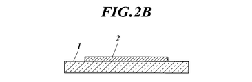
- FIG. 2A is a plan view showing a state where the organic functional layer 2 is formed on the support substrate 1
- FIG. 2B is a cross-sectional view taken along the line BB of FIG. 2A.
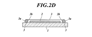
- 2C is a plan view showing a state in which the sealing adhesive 3 is disposed on the support substrate 1
- FIG. 2D is a cross-sectional view taken along the line DD in FIG. 2C.
- 2E is a plan view showing a state in which the sealing substrate 4 is disposed so as to contact the sealing adhesive 3
- FIG. 2F is a cross-sectional view taken along line FF in FIG. 2E.
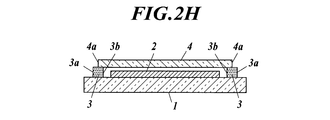
- FIG. 2G is a plan view showing a state after the sealing substrate 4 is cut
- FIG. 2H is a cross-sectional view taken along the line HH in FIG. 2G. 2A to 2H schematically show only the configuration (organic EL cell) corresponding to one organic functional layer 2 out of a plurality of organic functional layers 2 arranged in a matrix on the support substrate 1. ing.
- a support substrate 1 (see FIGS. 2A and 2B) on which an organic functional layer 2 is formed at a predetermined position on the upper surface is prepared, and the organic functional layer 2 is used using predetermined coating means (for example, screen printing).
- the sealing adhesive 3 is disposed so as to surround (disposing step; see FIGS. 2C and 2D). Specifically, the sealing adhesive 3 is disposed on the support substrate 1 so as to surround the organic functional layer 2 and so that the upper end protrudes upward from the upper surface of the organic functional layer 2.
- the sealing substrate 4 is covered so that the organic functional layer 2 on the supporting substrate 1 is covered from above and the upper end and the lower surface of the sealing adhesive 3 disposed on the supporting substrate 1 are brought into contact with each other.
- Arrange see FIGS. 2E and 2F.
- the sealing substrate 4 having a size substantially equal to that of the support substrate 1 is disposed, so that the organic functional layer 2 that is disposed in a matrix on the support substrate 1 is covered with all of the organic functional layers 2. To do.
- the position is located on the inner side of the outer end portion 3a of the sealing adhesive 3 of the sealing substrate 4 from the upper surface side of each sealing substrate 4 (FIG. 2F).
- the position indicated by the two arrows inside is cut using a predetermined cutting means (for example, a scribing method using a diamond wheel blade).
- a predetermined cutting means for example, a scribing method using a diamond wheel blade.
- the sealing adhesive 3 is cured using a predetermined curing means corresponding to the type of the sealing adhesive 3, and the sealing substrate 4 and the support substrate 1 are bonded via the sealing adhesive 3. Fix (fixing process). Thereby, the organic functional layer 2 on the support substrate 1 is sealed by the glass sealing substrate 4 through the sealing adhesive 3.
- the sealing adhesive 3 is made of glass so as to cover the organic functional layer 2 from the side opposite to the support substrate 1. 4 is fixed, and the outer end portion 4a of the sealing substrate 4 is arranged on the inner side of the outer end portion 3a of the sealing adhesive 3, so that the sealing adhesive fixed to the sealing substrate 4 is used. 3 and the support substrate 1 can be widened to increase the mechanical strength of the organic EL element 100 itself, and cracks C are formed on the lower surface of the outer end 4a of the sealing substrate 4. In this case, the sealing adhesive 3 can enter the inside of the crack C, and the outer end portion 4a where the stress of the sealing substrate 4 is easily concentrated can be appropriately protected by the sealing adhesive 3.
- the sealing substrate 4 and the support substrate 1 are made of a flexible substrate, and even if a bending stress is generated due to bending or the like, the crack C can be prevented from expanding. Therefore, even if the glass sealing substrate 4 has a smaller area than the support substrate 1, without performing a predetermined processing such as chamfering for improving the mechanical strength of the sealing substrate 4. Damage to the sealing substrate 4 can be suppressed.
- the sealing substrate 4 in contact with the sealing adhesive 3 is cut at a predetermined position inside the outer end portion 3a of the sealing adhesive 3, Since the outer end portion 4a of the sealing substrate 4 is arranged on the inner side of the outer end portion 3a of the sealing adhesive 3, even if the crack C is formed when the sealing substrate 4 is cut, the inner side of the crack C When the sealing adhesive 3 enters, the outer end portion 4 a of the sealing substrate 4 can be protected by the sealing adhesive 3.
- the sealing substrate 4 After the lower surface of the formed sealing substrate 4 is brought into contact with the sealing adhesive 3 on the support substrate 1, the sealing substrate 4 is pressed toward the support substrate 1, whereby the sealing adhesive 3.
- the outer end 3 a of the sealing substrate 4 is pushed out of the outer end 4 a of the sealing substrate 4.
- the left outer end 3 a of the sealing adhesive 3 is pushed to the left side of the left outer end 4 a of the sealing substrate 4, and the right outer end of the sealing adhesive 3
- the portion 3 a is pushed to the right side of the outer end portion 4 a on the right side of the sealing substrate 4, and the outer end portion 3 a on the front side of the sealing adhesive 3 is more than the outer end portion 4 a on the front side of the sealing substrate 4.
- the outer end portion 3a on the rear side of the sealing adhesive 3 is pushed further to the rear side than the outer end portion 4a on the rear side of the sealing substrate 4.
- the outer end portion 4 a of the sealing substrate 4 is structured to be disposed inside the outer end portion 3 a of the sealing adhesive 3.
- contact regulating means for regulating the contact between the organic functional layer 2 and the sealing adhesive 3 to be extruded may be provided.
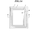
- FIGS. 3A to 3F are diagrams for explaining a modification of the sealing process of the organic functional layer 2 of the organic EL element 100.
- FIG. 3A is a plan view showing a state in which the sealing adhesive 3 is disposed on the support substrate 1
- FIG. 3B is a cross-sectional view taken along the line BB in FIG. 3A.
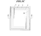
- 3C is a plan view showing a state in which the sealing substrate 4 is disposed so as to contact the sealing adhesive 3
- FIG. 3D is a cross-sectional view taken along the line DD of FIG. 3C.
- 3E is a plan view showing a state after the sealing substrate 4 is pressed
- FIG. 3F is a cross-sectional view taken along the line FF in FIG. 3E.
- a support substrate 1 (see FIGS. 2A and 2B) on which an organic functional layer 2 is formed at a predetermined position on the upper surface is prepared, and predetermined application means (for example, screen printing) is prepared in the same manner as in the above embodiment.
- the sealing adhesive 3 is disposed so as to surround the organic functional layer 2 using (a disposing step; see FIGS. 3A and 3B). Note that the amount of the sealing adhesive 3 disposed is larger than the amount of protrusion of the sealing adhesive 3 from the upper surface of the support substrate 1 in the disposing step (see FIG. 2D) of the above embodiment. preferable.
- the sealing substrate 4 is disposed so that the outer edge portion of the lower surface of each sealing substrate 4 is brought into contact with the upper end portion of each sealing adhesive 3 on the support substrate 1 (see FIGS. 3C and 3D). ). Specifically, the sealing substrate 4 is arranged so that the outer end portion 4 a of the sealing substrate 4 is superposed on the outer end portion 3 a of the sealing adhesive 3. Subsequently, before the sealing adhesive 3 is cured, the upper surface of the sealing substrate 4 is pressed toward the support substrate 1 (indicated by a white arrow in FIG. 3F), thereby The outer end portion 3a is pushed out of the outer end portion 4a of the sealing substrate 4 (in the direction indicated by two arrows in FIG. 3F).
- the outer end 4a of the sealing substrate 4 is placed inside the outer end 3a of the sealing adhesive 3 (see FIGS. 3E and 3F).
- the sealing adhesive 3 is not only pushed outward from the outer end portion 4a of the sealing substrate 4, but also moves so as to wrap around the lower end portion side of the side surface of the sealing substrate 4 to be pressed. Adhere.
- the sealing adhesive 3 is cured using a predetermined curing means corresponding to the type of the sealing adhesive 3, and the sealing substrate is interposed via the sealing adhesive 3. 4 and the support substrate 1 are fixed (fixing step).
- the support substrate 1 in contact with the sealing adhesive 3 is pressed so as to approach the sealing substrate 4 side, and the outer end 3 a of the sealing adhesive 3 is Since the outer end 4a of the sealing substrate 4 is disposed inside the outer end 3a of the sealing adhesive 3 by being pushed outward from the outer end 4a, the outer end of the sealing substrate 4 When the crack C is formed on the lower surface of the portion 4a, the sealing adhesive 4 is infiltrated into the crack C by a simple technique of pressing the sealing substrate 4, and the stress of the sealing substrate 4 is increased. Can be protected by the sealing adhesive 3.
- the sealing substrate 4 is pressed toward the support substrate 1 in order to push the outer end 3 a of the sealing adhesive 3 outward from the outer end 4 a of the sealing substrate 4.
- this is an example, and the present invention is not limited to this, and the support substrate 1 may be pressed toward the sealing substrate 4.
- the sealing method of the said embodiment and a modification may be performed in what kind of environment as long as it can prevent the penetration
- the sealing adhesive 3 was arrange
- the element 100 may be configured.
- the sealing adhesive 3 may be disposed in advance on the support substrate 1 before the sealing substrate 4 is disposed. That is, in the above embodiment and the modification, the sealing adhesive 3 is disposed so as to surround the organic functional layer 2 formed on the support substrate 1, but the seal is previously sealed at a predetermined position on the support substrate 1.
- the fixing adhesive 3 may be provided in an annular shape, and the organic functional layer 2 may be formed inside the annular sealing adhesive 3 before the sealing substrate 4 is provided.
- the sealing structure and sealing method for sealing an organic functional layer according to the present invention may be used in the manufacturing field in which an organic electroluminescence element is formed on a support substrate.
Landscapes
- Electroluminescent Light Sources (AREA)
Abstract
ガラス製の封止基板の破損を抑制する。 支持基板1の所定位置に形成された有機機能層を封止用接着剤3を介してガラス製の封止基板4により封止する有機EL素子100の封止構造であって、支持基板に、有機機能層を囲み、且つ、有機機能層の表面よりも支持基板と反対側に突出するように封止用接着剤が配設され、封止用接着剤には、支持基板と反対側から有機機能層を覆うように封止基板が固着され、封止用接着剤に固着された封止基板の外端部4aは、封止用接着剤の外端部3aよりも内側に配置されている。
Description
本発明は、有機エレクトロルミネッセンス素子(有機EL素子)に関し、支持基板に形成された有機機能層を封止する封止構造及び封止方法に関するものである。
近年、各種電子機器の表示ディスプレイや発光素子等においては、薄型化が図られるとともに視認性や耐衝撃性等に優れることから、有機EL素子の利用が進んでいる。
有機EL素子は、支持基板上に一対の電極に挟持された有機機能層を含む構成を有している。有機機能層は、機能の異なる複数の層が積層されており、例えば、正孔注入層、正孔輸送層、発光層、電子輸送層、電子注入層等を備えて構成されている。
有機EL素子は、支持基板上に一対の電極に挟持された有機機能層を含む構成を有している。有機機能層は、機能の異なる複数の層が積層されており、例えば、正孔注入層、正孔輸送層、発光層、電子輸送層、電子注入層等を備えて構成されている。
また、近年では、有機EL素子を平面状態だけでなく曲面状に湾曲させて使用する用途も増大しており、ガラス製の支持基板の薄型化に加えて可撓性基板の採用も検討されている。
ところで、有機機能層は、一般的に水分や酸素に対して極めて不安定であり、有機EL素子内に存在する水分や酸素は勿論のこと、素子の外部から侵入する水分や酸素によって劣化してしまうという問題がある。そこで、外部環境からの水分や酸素の侵入を阻止するために、極薄板ガラスの一面に透明樹脂層が貼着された封止材を用いて有機機能層を封止する手法が提案されている(例えば、特許文献1参照)。
なお、封止材の材料としては、ガラスの他にも、金属や樹脂等が知られているが、発光層からの光を封止材側から取り出すトップエミッション構造では、封止材に透明性が要求されることから、ガラスが封止材の材料としてよく用いられる。
ところで、有機機能層は、一般的に水分や酸素に対して極めて不安定であり、有機EL素子内に存在する水分や酸素は勿論のこと、素子の外部から侵入する水分や酸素によって劣化してしまうという問題がある。そこで、外部環境からの水分や酸素の侵入を阻止するために、極薄板ガラスの一面に透明樹脂層が貼着された封止材を用いて有機機能層を封止する手法が提案されている(例えば、特許文献1参照)。
なお、封止材の材料としては、ガラスの他にも、金属や樹脂等が知られているが、発光層からの光を封止材側から取り出すトップエミッション構造では、封止材に透明性が要求されることから、ガラスが封止材の材料としてよく用いられる。
しかしながら、上記特許文献1の場合、極薄板ガラスの厚さが10~70μmであることから、一面に透明樹脂層を貼着したとしても、製造される素子自体やパネルとしての強度不足が生じてしまう。特に、ガラスは、脆性材料であるため、薄型化に伴って機械的強度が低下してしまい、製造時や製造後の製品の取扱いが困難となる。
ここで、ガラス製の基板の破損は、基板自体に発生する引張応力と、当該ガラス表面に存する微少なクラックが原因であると考えられている。例えば、有機機能層をガラス製の封止基板を用いて封止した有機EL素子の場合、当該有機EL素子に発生する曲げ応力、具体的には、有機EL素子の屈曲等の際に外側に生じる引張応力が封止基板の表面に作用する。そして、封止基板の表面、特に、外端部に存するクラックに応力が集中すると、当該クラックが大きくなって当該封止基板の破損が生じてしまう。
なお、封止基板は、電極取り出しの関係上、支持基板よりも小面積とされ、当該封止基板の外端部に応力が集中し易い構造となっているとともに、ガラスの機械的強度を向上させるための当該封止基板の外端部に対する面取り加工等の処理も施し難くなっている。
ここで、ガラス製の基板の破損は、基板自体に発生する引張応力と、当該ガラス表面に存する微少なクラックが原因であると考えられている。例えば、有機機能層をガラス製の封止基板を用いて封止した有機EL素子の場合、当該有機EL素子に発生する曲げ応力、具体的には、有機EL素子の屈曲等の際に外側に生じる引張応力が封止基板の表面に作用する。そして、封止基板の表面、特に、外端部に存するクラックに応力が集中すると、当該クラックが大きくなって当該封止基板の破損が生じてしまう。
なお、封止基板は、電極取り出しの関係上、支持基板よりも小面積とされ、当該封止基板の外端部に応力が集中し易い構造となっているとともに、ガラスの機械的強度を向上させるための当該封止基板の外端部に対する面取り加工等の処理も施し難くなっている。
本発明は、上記課題に鑑みなされたものであり、その目的は、ガラス製の封止基板の破損を抑制することができる封止構造及び封止方法を提供することである。
上記課題を解決するため、請求項1に記載の発明の封止構造は、
支持基板の所定位置に形成された有機機能層を封止用接着剤を介してガラス製の封止基板により封止する封止構造であって、前記支持基板に、前記有機機能層を囲み、且つ、当該有機機能層の表面よりも前記支持基板と反対側に突出するように前記封止用接着剤が配設され、前記封止用接着剤には、前記支持基板と反対側から前記有機機能層を覆うように前記封止基板が固着され、前記封止用接着剤に固着された前記封止基板の外端部は、当該封止用接着剤の外端部よりも内側に配置されてなることを特徴としている。
支持基板の所定位置に形成された有機機能層を封止用接着剤を介してガラス製の封止基板により封止する封止構造であって、前記支持基板に、前記有機機能層を囲み、且つ、当該有機機能層の表面よりも前記支持基板と反対側に突出するように前記封止用接着剤が配設され、前記封止用接着剤には、前記支持基板と反対側から前記有機機能層を覆うように前記封止基板が固着され、前記封止用接着剤に固着された前記封止基板の外端部は、当該封止用接着剤の外端部よりも内側に配置されてなることを特徴としている。
請求項2に記載の発明は、請求項1に記載の封止構造において、
未硬化の前記封止用接着剤に接する封止基板が前記封止用接着剤の外端部よりも内側の所定位置で切断されることによって、前記封止基板の外端部が前記封止用接着剤の外端部よりも内側に配置されてなることを特徴としている。
未硬化の前記封止用接着剤に接する封止基板が前記封止用接着剤の外端部よりも内側の所定位置で切断されることによって、前記封止基板の外端部が前記封止用接着剤の外端部よりも内側に配置されてなることを特徴としている。
請求項3に記載の発明は、請求項1に記載の封止構造において、
未硬化の前記封止用接着剤に接する封止基板及び前記支持基板のうち、少なくとも一方が他方に相対的に近付くように押圧され、前記封止用接着剤の外端部が前記封止基板の外端部よりも外側に押し出されることによって、前記封止基板の外端部が前記封止用接着剤の外端部よりも内側に配置されてなることを特徴としている。
未硬化の前記封止用接着剤に接する封止基板及び前記支持基板のうち、少なくとも一方が他方に相対的に近付くように押圧され、前記封止用接着剤の外端部が前記封止基板の外端部よりも外側に押し出されることによって、前記封止基板の外端部が前記封止用接着剤の外端部よりも内側に配置されてなることを特徴としている。
請求項4に記載の発明は、請求項1~3の何れか一項に記載の封止構造において、
前記封止基板及び前記支持基板は、可撓性を有する基板であることを特徴としている。
前記封止基板及び前記支持基板は、可撓性を有する基板であることを特徴としている。
請求項5に記載の発明は、請求項4に記載の封止構造において、
前記封止基板の厚さは、200μm以下であることを特徴としている。
前記封止基板の厚さは、200μm以下であることを特徴としている。
請求項6に記載の発明の封止方法は、
支持基板の所定位置に形成される有機機能層を囲み、且つ、前記有機機能層の表面よりも前記支持基板と反対側に突出するように配設される封止用接着剤を介して、ガラス製の封止基板により前記有機機能層を封止する封止方法であって、
前記支持基板の所定位置に前記封止用接着剤を配設する配設工程と、
前記配設工程により配設された前記封止用接着剤に、前記支持基板と反対側から前記有機機能層を覆う前記封止基板を、当該封止基板の外端部が前記封止用接着剤の外端部よりも内側に配置されるように固着する固着工程とを行うことを特徴としている。
支持基板の所定位置に形成される有機機能層を囲み、且つ、前記有機機能層の表面よりも前記支持基板と反対側に突出するように配設される封止用接着剤を介して、ガラス製の封止基板により前記有機機能層を封止する封止方法であって、
前記支持基板の所定位置に前記封止用接着剤を配設する配設工程と、
前記配設工程により配設された前記封止用接着剤に、前記支持基板と反対側から前記有機機能層を覆う前記封止基板を、当該封止基板の外端部が前記封止用接着剤の外端部よりも内側に配置されるように固着する固着工程とを行うことを特徴としている。
本発明によれば、ガラス製の封止基板の破損を抑制することができる。
以下、本発明の実施形態について図面を参照して説明する。
図1は、本発明の封止構造を適用した一実施形態の有機EL素子100の一部分を模式的に示す斜視図である。
図1は、本発明の封止構造を適用した一実施形態の有機EL素子100の一部分を模式的に示す斜視図である。
図1に示すように、本実施形態の有機EL素子100は、支持基板1に形成されている有機機能層2(図2参照)を、封止用接着剤3を介して支持基板1と封止基板4とが接着されることで封止する構造を採っている。
なお、以下の説明では、支持基板1の有機機能層2が形成されている側を上側とし、反対側を下側とする。また、上下方向に直交する一方向を左右方向とし、上下方向及び左右方向の双方に直交する方向を前後方向とする。
なお、以下の説明では、支持基板1の有機機能層2が形成されている側を上側とし、反対側を下側とする。また、上下方向に直交する一方向を左右方向とし、上下方向及び左右方向の双方に直交する方向を前後方向とする。
支持基板1は、所定の材料から形成された可撓性を具備する基板である。即ち、支持基板1は、例えば、200μm程度の厚さに形成されることで、可撓性を具備する。
具体的には、支持基板1としては、例えば、樹脂フィルム、薄膜ガラス、金属箔等を適用することができる。
具体的には、支持基板1としては、例えば、樹脂フィルム、薄膜ガラス、金属箔等を適用することができる。
樹脂フィルムとしては、例えば、ポリエステルフィルム、ポリエチレンフィルム、ポリプロピレンフィルム、アイオノマーフィルム、ポリ塩化ビニルフィルム、ポリ塩化ビニリデンフィルム、ポリビニルアルコールフィルム、ポリカーボネートフィルム、ポリスチレンフィルム、ポリアクリロニトリルフィルム、エチレン酢酸ビニル共重合体フィルム、エチレン-ビニルアルコール共重合体フィルム、エチレン-メタクリル酸共重合体フィルム、ナイロン(登録商標)フィルム(ポリアミドフィルム)、ポリイミドフィルム、セロファンなどが挙げられる。
また、薄膜ガラスとしては、例えば、ケイ酸塩ガラスが用いられ、好ましくはシリカガラス、ホウ珪酸ガラスが用いられ、最も好ましくは無アルカリガラスが用いられる。また、薄膜ガラスは、可撓性を具備するように、例えば、オーバーフローダウンドロー法により長尺形状で肉薄(例えば、厚さが200μm程度)に成形されている。
金属箔の材料としては、例えばアルミニウム、銅、ニッケルなどの金属材料や、ステンレス、アルミニウム合金などの合金材料を用いることができ、可撓性を具備させる上での薄型化の加工性やコストの面ではアルミニウムが好ましい。
また、薄膜ガラスとしては、例えば、ケイ酸塩ガラスが用いられ、好ましくはシリカガラス、ホウ珪酸ガラスが用いられ、最も好ましくは無アルカリガラスが用いられる。また、薄膜ガラスは、可撓性を具備するように、例えば、オーバーフローダウンドロー法により長尺形状で肉薄(例えば、厚さが200μm程度)に成形されている。
金属箔の材料としては、例えばアルミニウム、銅、ニッケルなどの金属材料や、ステンレス、アルミニウム合金などの合金材料を用いることができ、可撓性を具備させる上での薄型化の加工性やコストの面ではアルミニウムが好ましい。
また、支持基板1の所定位置には、所定数の有機機能層2が形成されている。即ち、支持基板1には、例えば、各々が封止基板4により封止される有機機能層2がマトリックス状に複数配設されている。
なお、図1には、支持基板1の右側の端部に形成されている所定数の有機機能層2に対応する部分を拡大して示している。
なお、図1には、支持基板1の右側の端部に形成されている所定数の有機機能層2に対応する部分を拡大して示している。
各有機機能層2は、例えば、左右方向及び前後方向に略均一の厚さとなるように形成されている(図2B等参照)。また、有機機能層2は、例えば、支持基板1上に一対の電極(図示略)に挟持された構成を有している。具体的には、有機機能層2は、各種機能を有する複数の層が積層されてなり、例えば、図示は省略するが、正孔注入層、正孔輸送層、発光層、電子輸送層、電子注入層等を備えた構成が挙げられる。
なお、有機機能層2は、封止工程より前の成膜工程によって成膜される。また、有機機能層2の形成方法としては、例えば、蒸着法、スパッタ法、CVD、PVD、溶剤を用いた塗布法等の様々な方法が挙げられる。なお、蒸着法による成膜は、一般的に、真空下で行われることから、本実施形態においても、成膜工程及び封止工程が真空容器(図示略)内にて行われても良い。
なお、有機機能層2は、封止工程より前の成膜工程によって成膜される。また、有機機能層2の形成方法としては、例えば、蒸着法、スパッタ法、CVD、PVD、溶剤を用いた塗布法等の様々な方法が挙げられる。なお、蒸着法による成膜は、一般的に、真空下で行われることから、本実施形態においても、成膜工程及び封止工程が真空容器(図示略)内にて行われても良い。
封止用接着剤3は、支持基板1上の各有機機能層2を取り囲むように環状、例えば、略「ロ」字状に配設されている。
また、封止用接着剤3は、有機機能層2の表面(上面)よりも支持基板1と反対側(上側)に突出するように配設されている。即ち、封止用接着剤3の上下方向の厚さは、略等しくなっているとともに、有機機能層2の同方向の厚さよりも大きくなっている。これにより、当該封止用接着剤3よりも上側に設けられる封止基板4の下面と有機機能層2の上面との接触を防止している。
なお、封止用接着剤3の配設形状は一例であってこれに限られるものではなく、適宜任意に変更可能であり、例えば、有機機能層2の上面並びに左右及び前後の各側面を被覆するように配設されても良い。
また、封止用接着剤3は、有機機能層2の表面(上面)よりも支持基板1と反対側(上側)に突出するように配設されている。即ち、封止用接着剤3の上下方向の厚さは、略等しくなっているとともに、有機機能層2の同方向の厚さよりも大きくなっている。これにより、当該封止用接着剤3よりも上側に設けられる封止基板4の下面と有機機能層2の上面との接触を防止している。
なお、封止用接着剤3の配設形状は一例であってこれに限られるものではなく、適宜任意に変更可能であり、例えば、有機機能層2の上面並びに左右及び前後の各側面を被覆するように配設されても良い。
また、封止用接着剤3の組成は、特に限定されるものではなく、例えば、熱可塑性樹脂、熱硬化型樹脂、光硬化型樹脂、低融点ガラス等を適用することができる。
熱可塑性樹脂としては、例えば、高分子フィルムである低密度ポリエチレン(LDPE)、HDPE、線状低密度ポリエチレン(LLDPE)、中密度ポリエチレン、未延伸ポリプロピレン(CPP)、OPP、ONy、PET、セロファン、ポリビニルアルコール(PVA)、延伸ビニロン(OV)、エチレン-酢酸ビニル共重合体(EVOH)、エチレン-プロピレン共重合体、エチレン-アクリル酸共重合体、エチレン-メタクリル酸共重合体、塩化ビニリデン(PVDC)等が挙げられる。
熱硬化型樹脂としては、例えば、フェノール系樹脂、エポキシ系樹脂、メラミン系樹脂、ユリア系樹脂、不飽和ポリエステル系樹脂、アルキド系樹脂、アクリル系樹脂、シリコーン系樹脂、ポリウレタン系樹脂等が挙げられる。
光硬化型樹脂としては、例えば、エステルアクリレート、ウレタンアクリレート、エポキシアクリレート、メラミンアクリレート、アクリル樹脂アクリレート等の各種アクリレート、ウレタンポリエステル等の樹脂を用いたラジカル系接着剤や、エポキシ、ビニルエーテル等の樹脂を用いたカチオン系接着剤、チオール・エン付加型樹脂系接着剤等が挙げられる。これらのうち、酸素による阻害がなく、光照射後も重合反応が進行するカチオン硬化タイプの紫外線硬化型エポキシ樹脂接着剤が好ましい。
低融点ガラスとしては、公知のものを使用できるが、具体的には、ホウ酸塩、酸化鉛等の主成分からなるガラスを使用できる。これら低融点ガラスを使用する場合には、その軟化点温度以上で焼成を行うことが好ましい。
熱可塑性樹脂としては、例えば、高分子フィルムである低密度ポリエチレン(LDPE)、HDPE、線状低密度ポリエチレン(LLDPE)、中密度ポリエチレン、未延伸ポリプロピレン(CPP)、OPP、ONy、PET、セロファン、ポリビニルアルコール(PVA)、延伸ビニロン(OV)、エチレン-酢酸ビニル共重合体(EVOH)、エチレン-プロピレン共重合体、エチレン-アクリル酸共重合体、エチレン-メタクリル酸共重合体、塩化ビニリデン(PVDC)等が挙げられる。
熱硬化型樹脂としては、例えば、フェノール系樹脂、エポキシ系樹脂、メラミン系樹脂、ユリア系樹脂、不飽和ポリエステル系樹脂、アルキド系樹脂、アクリル系樹脂、シリコーン系樹脂、ポリウレタン系樹脂等が挙げられる。
光硬化型樹脂としては、例えば、エステルアクリレート、ウレタンアクリレート、エポキシアクリレート、メラミンアクリレート、アクリル樹脂アクリレート等の各種アクリレート、ウレタンポリエステル等の樹脂を用いたラジカル系接着剤や、エポキシ、ビニルエーテル等の樹脂を用いたカチオン系接着剤、チオール・エン付加型樹脂系接着剤等が挙げられる。これらのうち、酸素による阻害がなく、光照射後も重合反応が進行するカチオン硬化タイプの紫外線硬化型エポキシ樹脂接着剤が好ましい。
低融点ガラスとしては、公知のものを使用できるが、具体的には、ホウ酸塩、酸化鉛等の主成分からなるガラスを使用できる。これら低融点ガラスを使用する場合には、その軟化点温度以上で焼成を行うことが好ましい。
封止基板4は、例えば、各有機機能層2を囲む封止用接着剤3の各々に対応させるようにマトリックス状に複数配設されている。即ち、各封止基板4は、支持基板1上に有機機能層2を囲むように配設された各々の封止用接着剤3の上端部に当該封止基板4の下面の外縁部を接触させることで、当該下面を支持基板1上の有機機能層2の上面と対向させて配置されている。
また、各封止基板4は、封止用接着剤3の配設形状に対応させた形状をなし、例えば、直角四辺形状(例えば、正方形や長方形等)に形成されている。
なお、封止基板4の形状は、一例であってこれに限られるものではなく、適宜任意に変更可能である。
なお、封止基板4の形状は、一例であってこれに限られるものではなく、適宜任意に変更可能である。
また、各封止基板4は、その外端部4aが封止用接着剤3の外端部3aよりも内側、即ち、環状をなす封止用接着剤3の外端部3aと内端部3bの間に配置されるような寸法に形成されている。具体的には、各封止基板4は、左側の外端部4aの各々が封止用接着剤3の左側の外端部3aよりも右側に配置され、また、右側の外端部4aの各々が封止用接着剤3の右側の外端部3aよりも左側に配置され、また、前側の外端部4aの各々が封止用接着剤3の前側の外端部3aよりも後側に配置され、また、後側の外端部4aの各々が封止用接着剤3の後側の外端部3aよりも前側に配置されている。
また、封止基板4の外端部4aと封止用接着剤3の外端部3aとの所定方向(例えば、左右方向や前後方向等)に沿った距離は、例えば、封止基板4の組成(強度)や形状(特に、厚さ)、封止用接着剤3の組成(接着強度)、支持基板1の組成(強度)や形状等を考慮して適宜任意に変更可能である。具体的には、封止基板4の外端部4aと封止用接着剤3の外端部3aとの距離は、例えば、封止基板4の厚さに対して、10~1000%程度の長さとなっている。
また、封止基板4の外端部4aと封止用接着剤3の外端部3aとの所定方向(例えば、左右方向や前後方向等)に沿った距離は、例えば、封止基板4の組成(強度)や形状(特に、厚さ)、封止用接着剤3の組成(接着強度)、支持基板1の組成(強度)や形状等を考慮して適宜任意に変更可能である。具体的には、封止基板4の外端部4aと封止用接着剤3の外端部3aとの距離は、例えば、封止基板4の厚さに対して、10~1000%程度の長さとなっている。
また、封止基板4は、ガラスから形成された可撓性を具備する基板である。即ち、封止基板4は、例えば、支持基板1と略等しい厚さか、或いは、その厚さよりも薄く形成されることで、可撓性を具備する。具体的には、封止基板4の厚さは、例えば、200μm以下となっている。
なお、封止基板4の材料としてのガラスは、支持基板1と同様に、例えば、ケイ酸塩ガラス、シリカガラス、ホウ珪酸ガラス、無アルカリガラス等が挙げられる。
なお、封止基板4の材料としてのガラスは、支持基板1と同様に、例えば、ケイ酸塩ガラス、シリカガラス、ホウ珪酸ガラス、無アルカリガラス等が挙げられる。
また、封止基板4の表面には微小なクラックCが形成されている。
ここで、封止基板4にクラックCが形成される原因としては、ガラス基板の分断が挙げられる。ガラス基板を分断する方法として、例えば、ダイアモンドホイール刃によるスクライブ分断法やレーザー応力分断法等がある。即ち、有機EL素子100に用いられる封止基板4を製品寸法に切り出す場合、封止基板4を構成するガラス基板にホイール刃によるスクライブ線を入れ、ガラス基板のスクライブ線に基づく所定位置に応力が加えられることでガラス基板を分断する。このとき加えられた応力によって、ガラス基板(封止基板4)の表面にクラックCが形成され易くなる。
また、クラックCは、封止基板4の表面、特に、端部に形成され、例えば、封止基板4の支持基板1と対向する下面と何れか一の側面(例えば、右側面等)の二面に亘るものや、これらの二面に加えて上面の三面に亘るものなどがある(図1参照)。
ここで、封止基板4にクラックCが形成される原因としては、ガラス基板の分断が挙げられる。ガラス基板を分断する方法として、例えば、ダイアモンドホイール刃によるスクライブ分断法やレーザー応力分断法等がある。即ち、有機EL素子100に用いられる封止基板4を製品寸法に切り出す場合、封止基板4を構成するガラス基板にホイール刃によるスクライブ線を入れ、ガラス基板のスクライブ線に基づく所定位置に応力が加えられることでガラス基板を分断する。このとき加えられた応力によって、ガラス基板(封止基板4)の表面にクラックCが形成され易くなる。
また、クラックCは、封止基板4の表面、特に、端部に形成され、例えば、封止基板4の支持基板1と対向する下面と何れか一の側面(例えば、右側面等)の二面に亘るものや、これらの二面に加えて上面の三面に亘るものなどがある(図1参照)。
次に、有機EL素子100の有機機能層2の封止方法について、図2A~図2Hを参照して説明する。
この有機機能層2の封止方法では、支持基板1上で、有機機能層2を囲み、且つ、有機機能層2の表面よりも支持基板1と反対側に突出するように封止用接着剤3を配設する配設工程と、支持基板1と反対側から当該支持基板1に形成された有機機能層2を覆う封止基板4を、その外端部4aが封止用接着剤3の外端部3aよりも内側に配置されるように封止用接着剤3に固着する固着工程とを行う。
この有機機能層2の封止方法では、支持基板1上で、有機機能層2を囲み、且つ、有機機能層2の表面よりも支持基板1と反対側に突出するように封止用接着剤3を配設する配設工程と、支持基板1と反対側から当該支持基板1に形成された有機機能層2を覆う封止基板4を、その外端部4aが封止用接着剤3の外端部3aよりも内側に配置されるように封止用接着剤3に固着する固着工程とを行う。
図2A~図2Hは、有機EL素子100の有機機能層2の封止処理の一例を説明するための図である。このうち、図2Aは、支持基板1上に有機機能層2が形成された状態を示す平面図であり、図2Bは、図2AのB-B線における断面図である。また、図2Cは、支持基板1上に封止用接着剤3が配設された状態を示す平面図であり、図2Dは、図2CのD-D線における断面図である。また、図2Eは、封止用接着剤3に接触させるように封止基板4が配置された状態を示す平面図であり、図2Fは、図2EのF-F線における断面図である。また、図2Gは、封止基板4の切断後の状態を示す平面図であり、図2Hは、図2GのH-H線における断面図である。
なお、図2A~図2Hには、支持基板1にマトリックス状に複数配設される有機機能層2のうち、一の有機機能層2に対応する構成(有機ELセル)のみを模式的に示している。
なお、図2A~図2Hには、支持基板1にマトリックス状に複数配設される有機機能層2のうち、一の有機機能層2に対応する構成(有機ELセル)のみを模式的に示している。
先ず、例えば、上面の所定位置に有機機能層2が形成された支持基板1(図2A及び図2B参照)を用意し、所定の塗布手段(例えば、スクリーン印刷等)を用いて有機機能層2を囲むように封止用接着剤3を配設する(配設工程;図2C及び図2D参照)。具体的には、支持基板1上に、有機機能層2を取り囲むように環状に、且つ、上端部が有機機能層2の上面よりも上方向に突出するように封止用接着剤3を配設する。
次に、支持基板1上の有機機能層2を上方から覆い、且つ、支持基板1上に配設された封止用接着剤3の上端部と下面とを接触させるように封止基板4を配設する(図2E及び図2F参照)。具体的には、支持基板1と略等しい寸法の封止基板4が配設されることで、当該支持基板1にマトリックス状に複数配設されている有機機能層2の全てを覆った状態とする。
続けて、封止用接着剤3の硬化前に、各封止基板4の上面側から、当該封止基板4の封止用接着剤3の外端部3aよりも内側となる位置(図2F中の二つの矢印で示す位置)を、所定の切断手段(例えば、ダイアモンドホイール刃を用いたスクライブ法等)を用いて切断する。これにより、各封止基板4の外端部4aが、各封止用接着剤3の外端部3aよりも内側に配置されて、当該封止基板4の下面の外縁部が封止用接着剤3と接触した状態となる(図2G及び図2H参照)。
その後、封止用接着剤3の種類に対応する所定の硬化手段を用いて当該封止用接着剤3を硬化させ、封止用接着剤3を介して封止基板4と支持基板1とを固着させる(固着工程)。
これにより、支持基板1上の有機機能層2を封止用接着剤3を介してガラス製の封止基板4により封止する。
その後、封止用接着剤3の種類に対応する所定の硬化手段を用いて当該封止用接着剤3を硬化させ、封止用接着剤3を介して封止基板4と支持基板1とを固着させる(固着工程)。
これにより、支持基板1上の有機機能層2を封止用接着剤3を介してガラス製の封止基板4により封止する。
以上のように、本実施形態の有機EL素子100の封止構造によれば、封止用接着剤3に、支持基板1と反対側から有機機能層2を覆うようにガラス製の封止基板4が固着され、当該封止基板4の外端部4aが封止用接着剤3の外端部3aよりも内側に配置されているので、封止基板4と固着される封止用接着剤3と支持基板1との接触面積を広くして、有機EL素子100自体の機械的強度を向上させることができるだけでなく、封止基板4の外端部4aの下面にクラックCが形成されている場合に、クラックCの内側に封止用接着剤3を浸入させて当該封止基板4の応力が集中しやすい外端部4aを封止用接着剤3により適正に保護することができる。即ち、クラックCの内側に封止用接着剤3が浸入することにより当該封止用接着剤3と封止基板4との接触面積を大きくして、封止基板4の機械的強度を向上させることができ、封止基板4及び支持基板1が可撓性を有する基板から構成され、屈曲等により曲げ応力が発生しても、クラックCが拡大することを抑制することができる。
従って、ガラス製の封止基板4が支持基板1よりも小面積であっても、当該封止基板4の機械的強度を向上させるための面取り加工等の所定の加工処理を行うことなく、当該封止基板4の破損を抑制することができる。
従って、ガラス製の封止基板4が支持基板1よりも小面積であっても、当該封止基板4の機械的強度を向上させるための面取り加工等の所定の加工処理を行うことなく、当該封止基板4の破損を抑制することができる。
また、封止用接着剤3の硬化前に、封止用接着剤3に接する封止基板4が封止用接着剤3の外端部3aよりも内側の所定位置で切断されることによって、封止基板4の外端部4aが封止用接着剤3の外端部3aよりも内側に配置されるので、封止基板4の切断時にクラックCが形成されても、当該クラックCの内側に封止用接着剤3が浸入することにより、封止基板4の外端部4aを封止用接着剤3により保護することができる。
なお、本発明は、上記実施形態に限定されることなく、本発明の趣旨を逸脱しない範囲にて、種々の改良並びに設計の変更を行っても良い。
以下に、有機EL素子100の有機機能層2の封止処理の変形例について、図面を参照して説明する。また、変形例は、下記に詳細に説明する以外の点で、上記実施形態と略同様の構成をなし、その説明は省略する。
以下に、有機EL素子100の有機機能層2の封止処理の変形例について、図面を参照して説明する。また、変形例は、下記に詳細に説明する以外の点で、上記実施形態と略同様の構成をなし、その説明は省略する。
<変形例>
この有機EL素子100の有機機能層2の封止処理の変形例では、封止用接着剤3の硬化前に、封止用接着剤3に接する支持基板1及び封止基板4のうち、少なくとも一方が他方に相対的に近付くように押圧されることで、封止用接着剤3の外端部3aが封止基板4の外端部4aよりも外側に押し出される(図3F参照)。
即ち、所定の寸法(例えば、外端部4aが封止用接着剤3の外端部3aと上下に重なるか、或いは、その外端部3aよりも外側に配置される程度の寸法等)に形成された封止基板4の下面を支持基板1上の封止用接着剤3に接触させた後、当該封止基板4が支持基板1側に押圧されることで、封止用接着剤3の外端部3aが封止基板4の外端部4aよりも外側に押し出される。具体的には、封止用接着剤3の左側の外端部3aが封止基板4の左側の外端部4aよりも左側に押し出され、また、封止用接着剤3の右側の外端部3aが封止基板4の右側の外端部4aよりも右側に押し出され、また、封止用接着剤3の前側の外端部3aが封止基板4の前側の外端部4aよりも前側に押し出され、また、封止用接着剤3の後側の外端部3aが封止基板4の後側の外端部4aよりも後側に押し出される。これにより、封止基板4の外端部4aが封止用接着剤3の外端部3aよりも内側に配置された構造をなす。
この有機EL素子100の有機機能層2の封止処理の変形例では、封止用接着剤3の硬化前に、封止用接着剤3に接する支持基板1及び封止基板4のうち、少なくとも一方が他方に相対的に近付くように押圧されることで、封止用接着剤3の外端部3aが封止基板4の外端部4aよりも外側に押し出される(図3F参照)。
即ち、所定の寸法(例えば、外端部4aが封止用接着剤3の外端部3aと上下に重なるか、或いは、その外端部3aよりも外側に配置される程度の寸法等)に形成された封止基板4の下面を支持基板1上の封止用接着剤3に接触させた後、当該封止基板4が支持基板1側に押圧されることで、封止用接着剤3の外端部3aが封止基板4の外端部4aよりも外側に押し出される。具体的には、封止用接着剤3の左側の外端部3aが封止基板4の左側の外端部4aよりも左側に押し出され、また、封止用接着剤3の右側の外端部3aが封止基板4の右側の外端部4aよりも右側に押し出され、また、封止用接着剤3の前側の外端部3aが封止基板4の前側の外端部4aよりも前側に押し出され、また、封止用接着剤3の後側の外端部3aが封止基板4の後側の外端部4aよりも後側に押し出される。これにより、封止基板4の外端部4aが封止用接着剤3の外端部3aよりも内側に配置された構造をなす。
なお、当該封止基板4が支持基板1側に押圧されることで、封止用接着剤3の内端部3bが内側(有機機能層2側)に押し出されるため、例えば、支持基板1上の有機機能層2側に、当該有機機能層2と押し出される封止用接着剤3との接触を規制する接触規制手段(図示略)を設けても良い。
次に、有機EL素子100の有機機能層2の封止方法について、図3A~図3Fを参照して説明する。
図3A~図3Fは、有機EL素子100の有機機能層2の封止処理の変形例を説明するための図である。このうち、図3Aは、支持基板1上に封止用接着剤3が配設された状態を示す平面図であり、図3Bは、図3AのB-B線における断面図である。図3Cは、封止用接着剤3に接触させるように封止基板4が配置された状態を示す平面図であり、図3Dは、図3CのD-D線における断面図である。図3Eは、封止基板4の押圧後の状態を示す平面図であり、図3Fは、図3EのF-F線における断面図である。
図3A~図3Fは、有機EL素子100の有機機能層2の封止処理の変形例を説明するための図である。このうち、図3Aは、支持基板1上に封止用接着剤3が配設された状態を示す平面図であり、図3Bは、図3AのB-B線における断面図である。図3Cは、封止用接着剤3に接触させるように封止基板4が配置された状態を示す平面図であり、図3Dは、図3CのD-D線における断面図である。図3Eは、封止基板4の押圧後の状態を示す平面図であり、図3Fは、図3EのF-F線における断面図である。
先ず、例えば、上面の所定位置に有機機能層2が形成された支持基板1(図2A及び図2B参照)を用意し、上記実施形態と同様に、所定の塗布手段(例えば、スクリーン印刷等)を用いて有機機能層2を囲むように封止用接着剤3を配設する(配設工程;図3A及び図3B参照)。
なお、封止用接着剤3の配設量は、支持基板1上面からの封止用接着剤3の突出量が上記実施形態の配設工程(図2D参照)の場合よりも大きくなるのが好ましい。
なお、封止用接着剤3の配設量は、支持基板1上面からの封止用接着剤3の突出量が上記実施形態の配設工程(図2D参照)の場合よりも大きくなるのが好ましい。
次に、各封止基板4の下面の外縁部を支持基板1上の各封止用接着剤3の上端部と接触させるように当該封止基板4を配設する(図3C及び図3D参照)。具体的には、封止用接着剤3の外端部3aに封止基板4の外端部4aを上下に重ね合わせるようにして当該封止基板4を配置する。
続けて、封止用接着剤3の硬化前に、封止基板4の上面を支持基板1側(図3F中の白抜きの矢印で示す)に押圧することにより、封止用接着剤3の外端部3aを封止基板4の外端部4aよりも外側(図3F中の二つの矢印で示す方向)に押し出す。これにより、封止基板4の外端部4aが封止用接着剤3の外端部3aよりも内側に配置された状態となる(図3E及び図3F参照)。このとき、封止用接着剤3は、封止基板4の外端部4aよりも外側に押し出されるだけでなく、押圧される封止基板4の側面の下端部側にも回り込むように移動して付着する。
続けて、封止用接着剤3の硬化前に、封止基板4の上面を支持基板1側(図3F中の白抜きの矢印で示す)に押圧することにより、封止用接着剤3の外端部3aを封止基板4の外端部4aよりも外側(図3F中の二つの矢印で示す方向)に押し出す。これにより、封止基板4の外端部4aが封止用接着剤3の外端部3aよりも内側に配置された状態となる(図3E及び図3F参照)。このとき、封止用接着剤3は、封止基板4の外端部4aよりも外側に押し出されるだけでなく、押圧される封止基板4の側面の下端部側にも回り込むように移動して付着する。
その後、上記実施形態と同様に、封止用接着剤3の種類に対応する所定の硬化手段を用いて当該封止用接着剤3を硬化させ、封止用接着剤3を介して封止基板4と支持基板1とを固着させる(固着工程)。
従って、この変形例によれば、封止用接着剤3に接する支持基板1が封止基板4側に近付くように押圧され、封止用接着剤3の外端部3aが封止基板4の外端部4aよりも外側に押し出されることによって、封止基板4の外端部4aが封止用接着剤3の外端部3aよりも内側に配置されるので、封止基板4の外端部4aの下面にクラックCが形成されている場合に、封止基板4を押圧するという簡単な手法で、クラックCの内側に封止用接着剤3を浸入させて当該封止基板4の応力が集中しやすい外端部4aを封止用接着剤3により保護することができる。
よって、上記実施形態と同様に、ガラス製の封止基板4が支持基板1よりも小面積であっても、当該封止基板4の機械的強度を向上させるための面取り加工等の所定の加工処理を行うことなく、当該封止基板4の破損を抑制することができる。
よって、上記実施形態と同様に、ガラス製の封止基板4が支持基板1よりも小面積であっても、当該封止基板4の機械的強度を向上させるための面取り加工等の所定の加工処理を行うことなく、当該封止基板4の破損を抑制することができる。
なお、上記変形例では、封止用接着剤3の外端部3aを封止基板4の外端部4aよりも外側に押し出すために、封止基板4を支持基板1側に押圧するようにしたが、一例であってこれに限られるものではなく、支持基板1を封止基板4側に押圧するようにしても良い。
また、上記実施形態及び変形例の封止方法は、有機EL素子100の外部環境からの水分や酸素の侵入を阻止可能であれば如何なる環境で行われも良く、例えば、真空(低圧)環境であっても良いし、窒素等の不活性ガスにより置換された大気圧環境であっても良い。
さらに、上記実施形態及び変形例では、封止用接着剤3を環状に配設して中空構造の有機EL素子100を構成するようにしたが、一例であってこれに限られるものではなく、有機機能層2の上面並びに左右及び前後の各側面、当該有機機能層2の外側の支持基板1の上面が露出されている部分にも封止用接着剤3を充填して密封構造の有機EL素子100を構成しても良い。
また、封止用接着剤3は、封止基板4を配設する前であれば、支持基板1に予め配設しておいても良い。即ち、上記実施形態及び変形例では、支持基板1に形成された有機機能層2を囲むように封止用接着剤3を配設するようにしたが、予め支持基板1上の所定位置に封止用接着剤3を環状に配設しておき、封止基板4を配設する前に、環状の封止用接着剤3の内側に有機機能層2を形成するようにしても良い。
加えて、今回開示された実施形態は、全ての点で例示であって制限的なものではないと考えられるべきである。本発明の範囲は、上記した説明ではなくて特許請求の範囲によって示され、特許請求の範囲と均等の意味及び範囲内での全ての変更が含まれることが意図される。
本発明に係る有機機能層を封止する封止構造及び封止方法は、有機エレクトロルミネッセンス素子を支持基板に形成させる製造分野において利用可能性がある。
100 有機EL素子
1 支持基板
2 有機機能層
3 封止用接着剤
3a 外端部
4 封止基板
4a 外端部
1 支持基板
2 有機機能層
3 封止用接着剤
3a 外端部
4 封止基板
4a 外端部
Claims (6)
- 支持基板の所定位置に形成された有機機能層を封止用接着剤を介してガラス製の封止基板により封止する封止構造であって、
前記支持基板に、前記有機機能層を囲み、且つ、当該有機機能層の表面よりも前記支持基板と反対側に突出するように前記封止用接着剤が配設され、
前記封止用接着剤には、前記支持基板と反対側から前記有機機能層を覆うように前記封止基板が固着され、
前記封止用接着剤に固着された前記封止基板の外端部は、当該封止用接着剤の外端部よりも内側に配置されてなることを特徴とする封止構造。 - 未硬化の前記封止用接着剤に接する封止基板が前記封止用接着剤の外端部よりも内側の所定位置で切断されることによって、前記封止基板の外端部が前記封止用接着剤の外端部よりも内側に配置されてなることを特徴とする請求項1に記載の封止構造。
- 未硬化の前記封止用接着剤に接する封止基板及び前記支持基板のうち、少なくとも一方が他方に相対的に近付くように押圧され、前記封止用接着剤の外端部が前記封止基板の外端部よりも外側に押し出されることによって、前記封止基板の外端部が前記封止用接着剤の外端部よりも内側に配置されてなることを特徴とする請求項1に記載の封止構造。
- 前記封止基板及び前記支持基板は、可撓性を有する基板であることを特徴とする請求項1~3の何れか一項に記載の封止構造。
- 前記封止基板の厚さは、200μm以下であることを特徴とする請求項4に記載の封止構造。
- 支持基板の所定位置に形成される有機機能層を囲み、且つ、前記有機機能層の表面よりも前記支持基板と反対側に突出するように配設される封止用接着剤を介して、ガラス製の封止基板により前記有機機能層を封止する封止方法であって、
前記支持基板の所定位置に前記封止用接着剤を配設する配設工程と、
前記配設工程により配設された前記封止用接着剤に、前記支持基板と反対側から前記有機機能層を覆う前記封止基板を、当該封止基板の外端部が前記封止用接着剤の外端部よりも内側に配置されるように固着する固着工程とを行うことを特徴とする封止方法。
Applications Claiming Priority (2)
| Application Number | Priority Date | Filing Date | Title |
|---|---|---|---|
| JP2011135910 | 2011-06-20 | ||
| JP2011-135910 | 2011-06-20 |
Publications (1)
| Publication Number | Publication Date |
|---|---|
| WO2012176595A1 true WO2012176595A1 (ja) | 2012-12-27 |
Family
ID=47422435
Family Applications (1)
| Application Number | Title | Priority Date | Filing Date |
|---|---|---|---|
| PCT/JP2012/063887 Ceased WO2012176595A1 (ja) | 2011-06-20 | 2012-05-30 | 封止構造及び封止方法 |
Country Status (2)
| Country | Link |
|---|---|
| JP (1) | JPWO2012176595A1 (ja) |
| WO (1) | WO2012176595A1 (ja) |
Cited By (1)
| Publication number | Priority date | Publication date | Assignee | Title |
|---|---|---|---|---|
| JPWO2017094086A1 (ja) * | 2015-11-30 | 2018-09-13 | パイオニア株式会社 | 発光装置 |
Citations (5)
| Publication number | Priority date | Publication date | Assignee | Title |
|---|---|---|---|---|
| JPH11185956A (ja) * | 1997-12-18 | 1999-07-09 | Tdk Corp | 有機el素子の製造方法および有機el素子 |
| JP2007200846A (ja) * | 2006-01-27 | 2007-08-09 | Samsung Sdi Co Ltd | 有機電界発光表示装置及びその製造方法 |
| WO2010077412A1 (en) * | 2008-12-30 | 2010-07-08 | Vitex Systems, Inc. | Method for encapsulating environmentally sensitive devices |
| JP2011113704A (ja) * | 2009-11-25 | 2011-06-09 | Seiko Epson Corp | 有機el装置、有機el装置の製造方法、電子機器 |
| JP2011119169A (ja) * | 2009-12-07 | 2011-06-16 | Seiko Epson Corp | 電気光学装置、及び電気光学装置の製造方法 |
-
2012
- 2012-05-30 JP JP2013521511A patent/JPWO2012176595A1/ja active Pending
- 2012-05-30 WO PCT/JP2012/063887 patent/WO2012176595A1/ja not_active Ceased
Patent Citations (5)
| Publication number | Priority date | Publication date | Assignee | Title |
|---|---|---|---|---|
| JPH11185956A (ja) * | 1997-12-18 | 1999-07-09 | Tdk Corp | 有機el素子の製造方法および有機el素子 |
| JP2007200846A (ja) * | 2006-01-27 | 2007-08-09 | Samsung Sdi Co Ltd | 有機電界発光表示装置及びその製造方法 |
| WO2010077412A1 (en) * | 2008-12-30 | 2010-07-08 | Vitex Systems, Inc. | Method for encapsulating environmentally sensitive devices |
| JP2011113704A (ja) * | 2009-11-25 | 2011-06-09 | Seiko Epson Corp | 有機el装置、有機el装置の製造方法、電子機器 |
| JP2011119169A (ja) * | 2009-12-07 | 2011-06-16 | Seiko Epson Corp | 電気光学装置、及び電気光学装置の製造方法 |
Cited By (1)
| Publication number | Priority date | Publication date | Assignee | Title |
|---|---|---|---|---|
| JPWO2017094086A1 (ja) * | 2015-11-30 | 2018-09-13 | パイオニア株式会社 | 発光装置 |
Also Published As
| Publication number | Publication date |
|---|---|
| JPWO2012176595A1 (ja) | 2015-02-23 |
Similar Documents
| Publication | Publication Date | Title |
|---|---|---|
| KR101989940B1 (ko) | 발광 장치 및 발광 장치의 제작 방법 | |
| KR102334815B1 (ko) | 발광 장치 및 박리 방법 | |
| TWI808631B (zh) | 發光裝置 | |
| EP2685516B1 (en) | Method of manufacturing a display panel | |
| US8557637B2 (en) | Method for fabricating the flexible electronic device | |
| JP6285654B2 (ja) | 表示パネルの製造方法 | |
| US20150364718A1 (en) | Package structure for flexible organic light emitting diode device, method for packaging the same and flexible display device | |
| CN103177998B (zh) | 可挠式器件的取下方法 | |
| US9490448B2 (en) | OLED device packaging method and OLED device packaged with same | |
| US9853243B2 (en) | Flexible display and method for fabricating the same | |
| CN104600092B (zh) | Oled触控显示装置及其制造方法 | |
| CN108461523B (zh) | 有机发光二极管显示面板及其制作方法 | |
| CN110265580A (zh) | 一种柔性显示装置及其制备方法 | |
| TWI596756B (zh) | 用於顯示面板的母面板及使用該母面板製造顯示面板之方法 | |
| TWI470704B (zh) | 環境敏感電子元件的封裝方法 | |
| KR101596725B1 (ko) | 충전 필름 및 이를 이용한 유기 발광 디스플레이 장치의 제조 방법 | |
| WO2016143636A1 (ja) | 積層体及びその製造方法 | |
| JP2017024368A (ja) | 積層体及びその製造方法並びに電子デバイス及びその製造方法 | |
| KR102003769B1 (ko) | 유기 발광 표시 장치의 봉지용 금속 시트 및 그것을 이용한 봉지 방법 | |
| JP2018025776A (ja) | フレキシブル表示器及びキャリア基板の分離方法 | |
| KR102397800B1 (ko) | 측변 구부림 구조를 갖는 표시 장치 및 그 제조 방법 | |
| KR101947070B1 (ko) | 플렉서블 필름을 이용한 표시장치의 제조 방법 | |
| WO2012176595A1 (ja) | 封止構造及び封止方法 | |
| US20140220313A1 (en) | Light blocking sheet, method for manufacturing light blocking sheet, and transparent display device | |
| JP2016096218A (ja) | 積層基板の製造方法及び電子デバイスの製造方法 |
Legal Events
| Date | Code | Title | Description |
|---|---|---|---|
| 121 | Ep: the epo has been informed by wipo that ep was designated in this application |
Ref document number: 12803114 Country of ref document: EP Kind code of ref document: A1 |
|
| ENP | Entry into the national phase |
Ref document number: 2013521511 Country of ref document: JP Kind code of ref document: A |
|
| NENP | Non-entry into the national phase |
Ref country code: DE |
|
| 122 | Ep: pct application non-entry in european phase |
Ref document number: 12803114 Country of ref document: EP Kind code of ref document: A1 |