WO2012172986A1 - 半導体素子、半導体素子の製造方法、発光ダイオード、発光ダイオードの製造方法、光電変換素子、太陽電池、照明装置、バックライトおよび表示装置 - Google Patents
半導体素子、半導体素子の製造方法、発光ダイオード、発光ダイオードの製造方法、光電変換素子、太陽電池、照明装置、バックライトおよび表示装置 Download PDFInfo
- Publication number
- WO2012172986A1 WO2012172986A1 PCT/JP2012/064088 JP2012064088W WO2012172986A1 WO 2012172986 A1 WO2012172986 A1 WO 2012172986A1 JP 2012064088 W JP2012064088 W JP 2012064088W WO 2012172986 A1 WO2012172986 A1 WO 2012172986A1
- Authority
- WO
- WIPO (PCT)
- Prior art keywords
- core
- conductivity type
- type semiconductor
- shell
- semiconductor
- Prior art date
- Legal status (The legal status is an assumption and is not a legal conclusion. Google has not performed a legal analysis and makes no representation as to the accuracy of the status listed.)
- Ceased
Links
Images
















Classifications
-
- H—ELECTRICITY
- H10—SEMICONDUCTOR DEVICES; ELECTRIC SOLID-STATE DEVICES NOT OTHERWISE PROVIDED FOR
- H10H—INORGANIC LIGHT-EMITTING SEMICONDUCTOR DEVICES HAVING POTENTIAL BARRIERS
- H10H20/00—Individual inorganic light-emitting semiconductor devices having potential barriers, e.g. light-emitting diodes [LED]
- H10H20/80—Constructional details
- H10H20/81—Bodies
- H10H20/817—Bodies characterised by the crystal structures or orientations, e.g. polycrystalline, amorphous or porous
-
- H—ELECTRICITY
- H10—SEMICONDUCTOR DEVICES; ELECTRIC SOLID-STATE DEVICES NOT OTHERWISE PROVIDED FOR
- H10F—INORGANIC SEMICONDUCTOR DEVICES SENSITIVE TO INFRARED RADIATION, LIGHT, ELECTROMAGNETIC RADIATION OF SHORTER WAVELENGTH OR CORPUSCULAR RADIATION
- H10F10/00—Individual photovoltaic cells, e.g. solar cells
- H10F10/10—Individual photovoltaic cells, e.g. solar cells having potential barriers
- H10F10/14—Photovoltaic cells having only PN homojunction potential barriers
-
- H—ELECTRICITY
- H10—SEMICONDUCTOR DEVICES; ELECTRIC SOLID-STATE DEVICES NOT OTHERWISE PROVIDED FOR
- H10F—INORGANIC SEMICONDUCTOR DEVICES SENSITIVE TO INFRARED RADIATION, LIGHT, ELECTROMAGNETIC RADIATION OF SHORTER WAVELENGTH OR CORPUSCULAR RADIATION
- H10F30/00—Individual radiation-sensitive semiconductor devices in which radiation controls the flow of current through the devices, e.g. photodetectors
- H10F30/20—Individual radiation-sensitive semiconductor devices in which radiation controls the flow of current through the devices, e.g. photodetectors the devices having potential barriers, e.g. phototransistors
- H10F30/21—Individual radiation-sensitive semiconductor devices in which radiation controls the flow of current through the devices, e.g. photodetectors the devices having potential barriers, e.g. phototransistors the devices being sensitive to infrared, visible or ultraviolet radiation
- H10F30/22—Individual radiation-sensitive semiconductor devices in which radiation controls the flow of current through the devices, e.g. photodetectors the devices having potential barriers, e.g. phototransistors the devices being sensitive to infrared, visible or ultraviolet radiation the devices having only one potential barrier, e.g. photodiodes
- H10F30/221—Individual radiation-sensitive semiconductor devices in which radiation controls the flow of current through the devices, e.g. photodetectors the devices having potential barriers, e.g. phototransistors the devices being sensitive to infrared, visible or ultraviolet radiation the devices having only one potential barrier, e.g. photodiodes the potential barrier being a PN homojunction
-
- H—ELECTRICITY
- H10—SEMICONDUCTOR DEVICES; ELECTRIC SOLID-STATE DEVICES NOT OTHERWISE PROVIDED FOR
- H10F—INORGANIC SEMICONDUCTOR DEVICES SENSITIVE TO INFRARED RADIATION, LIGHT, ELECTROMAGNETIC RADIATION OF SHORTER WAVELENGTH OR CORPUSCULAR RADIATION
- H10F71/00—Manufacture or treatment of devices covered by this subclass
-
- H—ELECTRICITY
- H10—SEMICONDUCTOR DEVICES; ELECTRIC SOLID-STATE DEVICES NOT OTHERWISE PROVIDED FOR
- H10F—INORGANIC SEMICONDUCTOR DEVICES SENSITIVE TO INFRARED RADIATION, LIGHT, ELECTROMAGNETIC RADIATION OF SHORTER WAVELENGTH OR CORPUSCULAR RADIATION
- H10F77/00—Constructional details of devices covered by this subclass
- H10F77/10—Semiconductor bodies
- H10F77/14—Shape of semiconductor bodies; Shapes, relative sizes or dispositions of semiconductor regions within semiconductor bodies
- H10F77/147—Shapes of bodies
-
- H—ELECTRICITY
- H10—SEMICONDUCTOR DEVICES; ELECTRIC SOLID-STATE DEVICES NOT OTHERWISE PROVIDED FOR
- H10F—INORGANIC SEMICONDUCTOR DEVICES SENSITIVE TO INFRARED RADIATION, LIGHT, ELECTROMAGNETIC RADIATION OF SHORTER WAVELENGTH OR CORPUSCULAR RADIATION
- H10F77/00—Constructional details of devices covered by this subclass
- H10F77/10—Semiconductor bodies
- H10F77/14—Shape of semiconductor bodies; Shapes, relative sizes or dispositions of semiconductor regions within semiconductor bodies
- H10F77/148—Shapes of potential barriers
-
- H—ELECTRICITY
- H10—SEMICONDUCTOR DEVICES; ELECTRIC SOLID-STATE DEVICES NOT OTHERWISE PROVIDED FOR
- H10F—INORGANIC SEMICONDUCTOR DEVICES SENSITIVE TO INFRARED RADIATION, LIGHT, ELECTROMAGNETIC RADIATION OF SHORTER WAVELENGTH OR CORPUSCULAR RADIATION
- H10F77/00—Constructional details of devices covered by this subclass
- H10F77/20—Electrodes
- H10F77/206—Electrodes for devices having potential barriers
- H10F77/211—Electrodes for devices having potential barriers for photovoltaic cells
-
- H—ELECTRICITY
- H10—SEMICONDUCTOR DEVICES; ELECTRIC SOLID-STATE DEVICES NOT OTHERWISE PROVIDED FOR
- H10F—INORGANIC SEMICONDUCTOR DEVICES SENSITIVE TO INFRARED RADIATION, LIGHT, ELECTROMAGNETIC RADIATION OF SHORTER WAVELENGTH OR CORPUSCULAR RADIATION
- H10F77/00—Constructional details of devices covered by this subclass
- H10F77/20—Electrodes
- H10F77/244—Electrodes made of transparent conductive layers, e.g. transparent conductive oxide [TCO] layers
-
- H—ELECTRICITY
- H10—SEMICONDUCTOR DEVICES; ELECTRIC SOLID-STATE DEVICES NOT OTHERWISE PROVIDED FOR
- H10H—INORGANIC LIGHT-EMITTING SEMICONDUCTOR DEVICES HAVING POTENTIAL BARRIERS
- H10H20/00—Individual inorganic light-emitting semiconductor devices having potential barriers, e.g. light-emitting diodes [LED]
- H10H20/80—Constructional details
- H10H20/81—Bodies
- H10H20/819—Bodies characterised by their shape, e.g. curved or truncated substrates
- H10H20/821—Bodies characterised by their shape, e.g. curved or truncated substrates of the light-emitting regions, e.g. non-planar junctions
-
- H—ELECTRICITY
- H10—SEMICONDUCTOR DEVICES; ELECTRIC SOLID-STATE DEVICES NOT OTHERWISE PROVIDED FOR
- H10W—GENERIC PACKAGES, INTERCONNECTIONS, CONNECTORS OR OTHER CONSTRUCTIONAL DETAILS OF DEVICES COVERED BY CLASS H10
- H10W72/00—Interconnections or connectors in packages
- H10W72/01—Manufacture or treatment
- H10W72/0198—Manufacture or treatment batch processes
-
- Y—GENERAL TAGGING OF NEW TECHNOLOGICAL DEVELOPMENTS; GENERAL TAGGING OF CROSS-SECTIONAL TECHNOLOGIES SPANNING OVER SEVERAL SECTIONS OF THE IPC; TECHNICAL SUBJECTS COVERED BY FORMER USPC CROSS-REFERENCE ART COLLECTIONS [XRACs] AND DIGESTS
- Y02—TECHNOLOGIES OR APPLICATIONS FOR MITIGATION OR ADAPTATION AGAINST CLIMATE CHANGE
- Y02E—REDUCTION OF GREENHOUSE GAS [GHG] EMISSIONS, RELATED TO ENERGY GENERATION, TRANSMISSION OR DISTRIBUTION
- Y02E10/00—Energy generation through renewable energy sources
- Y02E10/50—Photovoltaic [PV] energy
- Y02E10/547—Monocrystalline silicon PV cells
Definitions
- the present invention relates to a rod-shaped semiconductor element, a manufacturing method thereof, a light emitting diode using such a semiconductor element, a manufacturing method of the light emitting diode, a photoelectric conversion element, a solar cell, a lighting device, a backlight, and a display device.
- Patent Document 1 Japanese Patent Laid-Open No. 2008-2008. -53730 is a nanowire photovoltaic device.
- FIG. 45 is a diagram for explaining the basic configuration of the nanowire photovoltaic device 900.
- a bottom contact 906 is formed on a substrate 908, and an elongated nanostructure 901 (first conductivity type semiconductor core) made of a first conductivity type semiconductor material.
- first conductivity type semiconductor core first conductivity type semiconductor core
- porous nanotemplate 902 formed on the lower contact 906.
- a conformal layer 903 (second conductivity type semiconductor shell) made of a second conductivity type semiconductor material is formed around the nanostructure 901, and the conductive transparent material 904 and the upper contact are formed on the conformal layer 903. 905 is formed.
- the elongated nanostructure 901 is formed by growing a metal nanoparticle serving as a catalyst by a CVD (Chemical Vapor Deposition) method or the like.
- the semiconductor element is configured by the first conductive type semiconductor core and the second conductive type semiconductor shell formed so as to cover the first conductive type core.
- the area of the PN junction is increased to obtain high power generation efficiency.
- the first conductive type semiconductor core (elongated nanostructure) is grown using a metal catalyst, it is unavoidable that crystal defects are caused by contamination with metal atoms serving as the catalyst. Such a crystal defect forms a deep level in a PN junction composed of a first conductivity type semiconductor core and a second conductivity type semiconductor shell (conformal layer 903), and causes a carrier defect. This results in a decrease in the efficiency of the solar cell due to recombination.
- the elongated nanostructure 901 gradually grows on the substrate with the metal nanoparticles serving as a catalyst as a growth point. Therefore, the lower part (substrate side) of the elongated nanostructure 901 is formed in the initial stage of growth, and the upper part is formed in the late stage. That is, the formation time differs between the lower part and the upper part of the elongated nanostructure 901. Therefore, the crystallinity of the first-conductivity-type semiconductor core (elongated nanostructure 901) tends to be non-uniform, resulting in non-uniform quality of the PN junction formed on the side surface of the first-conductivity-type semiconductor core. There was a problem that it was easy to become.
- this problem becomes particularly prominent when a PN junction is formed over a wide range on the side surface of the first conductivity type semiconductor core.
- an object of the present invention is to provide a semiconductor element having a good PN junction on the side surface and having good electrical characteristics.
- the subject of this invention is the manufacturing method of such a semiconductor element, the light emitting diode using such a semiconductor element, the manufacturing method of the light emitting diode, the photoelectric conversion element using such a semiconductor element, a solar cell,
- An object is to provide an illumination device, a backlight, and a display device.
- the semiconductor element of the present invention is A rod-shaped core, A first conductivity type semiconductor shell disposed to cover at least a part of the outer peripheral surface of the core; And a second conductivity type semiconductor shell arranged to cover at least a part of the outer peripheral surface of the first conductivity type semiconductor shell.
- the function as the core of the semiconductor element and the function as one side of the PN junction are the first conductive type semiconductor core, It can be shared by the conductive type semiconductor shell. Therefore, other characteristics of the rod-shaped semiconductor element can be improved while maintaining the characteristics of the PN junction constituted by the first conductivity type semiconductor shell and the second conductivity type semiconductor shell, In addition, manufacturing costs can be reduced. Further, by improving the characteristics of the PN junction, for example, when a semiconductor element is used as a photoelectric conversion element, the conversion efficiency can be improved, and when the semiconductor element is used as a light emitting diode, the light emission efficiency is improved. Can be made.
- the rod-shaped core and the first conductivity type semiconductor shell each share the function as the core of the semiconductor element and the function as one side of the PN junction. Can be fulfilled. Therefore, other characteristics of the rod-shaped semiconductor element can be improved at the same time while maintaining the characteristics of the PN junction composed of the first conductivity type semiconductor shell and the second conductivity type semiconductor shell. Also, the manufacturing cost can be reduced. Further, by improving the characteristics of the PN junction, for example, when a semiconductor element is used as a photoelectric conversion element, the conversion efficiency can be improved, and when used as a light emitting diode, the light emission efficiency can be improved. it can.
- the core is a first conductivity type semiconductor core
- the concentration of impurities imparting conductivity to the semiconductor core is higher than the concentration of impurities imparting conductivity to the semiconductor shell of the first conductivity type.
- the semiconductor element of the present invention is a rod-like semiconductor element and the shape of the first conductive type semiconductor core is elongated, it is important to keep the resistance of the first conductive type semiconductor core sufficiently low. This is because, when the resistance of the first conductivity type semiconductor core is not sufficiently low, a voltage drop occurs in the first conductivity type semiconductor core, causing deterioration of the characteristics of the semiconductor element. For example, when the semiconductor element is a solar cell, the power generation efficiency is deteriorated, and when the semiconductor element is a light emitting diode, the light emission efficiency is deteriorated.
- the characteristics of the PN junction constituted by the first conductivity type semiconductor shell and the second conductivity type semiconductor shell can be improved, and the resistance of the first conductivity type semiconductor core can be sufficiently increased. It becomes possible to make it small.
- the good characteristics of the PN junction and the goodness of the first conductivity type semiconductor core This is because it is possible to obtain a good balance between electrical conductivity.
- the core is a first conductivity type semiconductor core
- the resistivity of the semiconductor core is smaller than the resistivity of the first conductivity type semiconductor shell.
- the resistance of the first conductivity type semiconductor core is small, the characteristics of the PN junction constituted by the first conductivity type semiconductor shell and the second conductivity type semiconductor shell can be further improved. .
- the semiconductor shell of the first conductivity type is made of a material different from that of the core,
- the crystal defect density of the first conductivity type semiconductor shell is smaller than the crystal defect density of the core.
- the function as the core of the semiconductor element and the function as one side of the PN junction can be shared by the rod-shaped core and the first conductivity type semiconductor shell.
- the light emitting diode of the present invention is The semiconductor element of the present invention is provided.
- the light emission efficiency of the light emitting diode can be improved.
- a light emitting layer is provided between the first conductive type semiconductor shell and the second conductive type semiconductor shell.
- the light emission efficiency of the light emitting diode can be further improved.
- the band gap of the substance constituting the core is larger than the band gap of the substance constituting the light emitting layer.
- light generated in the light emitting layer is hardly absorbed by the rod-shaped core or the first conductivity type semiconductor core, so that the light emitting efficiency of the light emitting diode can be increased.
- a substrate A plurality of the semiconductor elements disposed on the substrate; Wiring for electrically connecting the semiconductor elements.
- the arrangement interval of the semiconductor elements having the function of light emitting diodes can be freely set on the substrate. Therefore, both the efficiency and reliability of the light emitting diode can be improved by efficiently escaping the semiconductor element having the function of the light emitting diode to the substrate and suppressing the temperature rise of the light emitting diode.
- the photoelectric conversion element of the present invention is The semiconductor element of the present invention is provided.
- the conversion efficiency of the photoelectric conversion element can be improved.
- a method for manufacturing a semiconductor element of the present invention includes A core forming step of forming a rod-shaped core on the substrate; A first shell forming step of covering at least a part of the outer peripheral surface of the rod-shaped core with a semiconductor shell of a first conductivity type; And a second shell forming step of covering at least a part of the outer peripheral surface of the first conductivity type shell with a second conductivity type semiconductor shell.
- the first conductivity type semiconductor shell is formed after the rod-shaped semiconductor core is formed, the first conductivity type semiconductor having uniform and good crystallinity is formed on the surface of the first conductivity type semiconductor shell. Is exposed. Thereafter, since at least a part of the outer peripheral surface of the first conductivity type shell is covered with the second conductivity type semiconductor shell, the first conductivity type semiconductor shell and the second conductivity type semiconductor shell have good characteristics. A PN junction can be obtained.
- the rod-shaped core is separately formed prior to the formation of the first conductivity type semiconductor shell, the rod-shaped core can have a property suitable for fulfilling the function as the core of the rod-shaped semiconductor element.
- the function as the core of the rod-shaped semiconductor element and the function as one side of the PN junction can be shared by the first conductivity type semiconductor core and the first conductivity type semiconductor shell. Therefore, it is possible to improve other characteristics of the rod-shaped semiconductor element while maintaining the characteristics of the PN junction composed of the first conductivity type semiconductor shell and the second conductivity type semiconductor shell, The manufacturing cost can be reduced. Further, by improving the characteristics of the PN junction, for example, when a semiconductor element is used as a photoelectric conversion element, the conversion efficiency is improved, and when it is used as a light emitting diode, the light emission efficiency is improved.
- the core forming step includes etching a part of a material constituting the core formed on the substrate.
- the cross-sectional shape of the rod-shaped core can be freely changed. Therefore, for example, the crystal orientation of the side surface of the rod-shaped core can be made favorable, and the characteristics of the semiconductor element can be improved.
- Annealing is performed after the core step and before the first shell forming step.
- crystallinity can be improved by recovering the crystal defects of the rod-shaped core. Therefore, it is possible to further improve the crystallinity of the first conductivity type semiconductor shell to be formed in the first shell formation step performed later.
- a part of the core formed in the core formation step is removed by wet etching.
- crystallinity can be improved by recovering the crystal defects of the rod-shaped core. Therefore, it is possible to further improve the crystallinity of the first conductivity type semiconductor shell formed in the first shell formation step performed later.
- a rod-shaped core is grown on the substrate.
- the substrate and the rod-shaped core are in contact with each other with the same area as the cross-sectional area of the rod-shaped core.
- the diameter of the rod-shaped core is from nanoscale to microscale, the cross-sectional area is small.
- the rod-shaped cores are discretely formed on the substrate. Therefore, warpage of the substrate due to mismatch of lattice constants between the material constituting the substrate and the material constituting the rod-shaped core can be suppressed. Therefore, the accuracy of the photolithography process in the process for forming the semiconductor element can be improved, and the yield of the semiconductor element can be improved.
- an annealing process at a temperature higher than the temperature for forming the core is performed.
- the crystallinity can be improved by recovering the rod-like crystal defects, so that the crystallinity of the second-conductivity-type semiconductor shell and the light emitting layer formed thereafter is excellent. Can be.
- the method for manufacturing the light emitting diode of the present invention includes: A core forming step of forming a plurality of rod-shaped cores on the first substrate; A first shell forming step of covering at least a part of the outer peripheral surfaces of the plurality of rod-shaped cores with a first conductivity type semiconductor shell; A second shell forming step of covering at least a part of the outer peripheral surface of the first conductivity type semiconductor shell with a second conductivity type semiconductor shell; Each of the rod-shaped cores, the first conductivity type semiconductor shell covering the cores, and the second conductivity type semiconductor covering the first conductivity type semiconductor shells covering the cores.
- a semiconductor element separation step of separating the integral structure with the shell from the first substrate for each of the rod-shaped cores and taking out a plurality of semiconductor elements; And a semiconductor element arranging step of arranging a plurality of the semiconductor elements on the second substrate.
- a semiconductor element as a constituent element is covered with a first conductivity type semiconductor shell and a second conductivity type shell after a rod-shaped core is formed on a first substrate. Therefore, the PN junction area per unit substrate area, that is, the light emission area can be greatly increased, and the manufacturing cost can be reduced.
- the rod-shaped core is formed of the first conductive type semiconductor shell. Since it is formed separately prior to formation, the rod-shaped core can be formed to have a property suitable for functioning as a core of a rod-shaped semiconductor element. Therefore, other characteristics of the rod-shaped semiconductor element can be improved while maintaining the characteristics of the PN junction constituted by the first conductivity type semiconductor shell and the second conductivity type semiconductor shell.
- the arrangement interval of the semiconductor elements having the function of light-emitting diodes can be freely set. Therefore, both the efficiency and reliability of the light emitting diode can be improved by efficiently escaping the semiconductor element having the function of the light emitting diode to the substrate and suppressing the temperature rise of the light emitting diode. Therefore, a highly efficient and highly reliable light emitting diode can be manufactured at low cost.
- the solar cell of the present invention is characterized by including the photoelectric conversion element of the present invention.
- the power generation efficiency of the solar cell can be increased.
- the lighting device of the present invention is characterized by including the light emitting diode of the present invention.
- the backlight of the present invention is characterized by including the light emitting diode of the present invention.
- the display device of the present invention is characterized by including the light emitting diode of the present invention.
- the function as the core of the semiconductor element and the function as one side of the PN junction can be shared by the rod-shaped core and the first conductivity type semiconductor shell. Therefore, other characteristics of the rod-shaped semiconductor element can be improved while maintaining the characteristics of the PN junction constituted by the first conductivity type semiconductor shell and the second conductivity type semiconductor shell, In addition, manufacturing costs can be reduced. Further, by improving the characteristics of the PN junction, for example, when a semiconductor element is used as a photoelectric conversion element, the conversion efficiency can be improved, and when used as a light emitting diode, the light emission efficiency can be improved. it can.
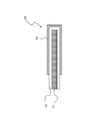
- FIG. 1 is a longitudinal sectional view including a central axis of a semiconductor element 10 having an elongated rod-like shape according to a first embodiment of the present invention
- FIG. 2 is a radial sectional view of the semiconductor element 10. .
- the semiconductor element 10 includes a rod-shaped first conductive type semiconductor core 11, a first conductive type semiconductor shell 12, and a second conductive type semiconductor shell 13.
- the first-conductivity-type semiconductor shell 12 covers the entire side surface of the rod-shaped first-conductivity-type semiconductor core 11 (the entire outer peripheral surface of the rod-shaped semiconductor-core 11) and one end.
- the shell 13 covers the surface of the first conductivity type semiconductor shell 12.
- the second conductivity type semiconductor shell 13 does not cover the entire surface of the first conductivity type semiconductor shell 12 and does not cover the other end portion 19 of the rod-shaped first conductivity type semiconductor core 11. Yes.
- the second conductive type semiconductor shell 13 covers only a part of the outer peripheral surface of the first conductive type semiconductor shell 12.
- FIG. 2 is a cross-sectional view in the diameter direction in a region where the surface of the first conductivity type semiconductor shell 12 is covered by the second conductivity type semiconductor shell 13.
- the interface between the first conductivity type semiconductor shell 12 and the second conductivity type semiconductor shell 13 constitutes a PN junction. Since the second conductivity type semiconductor shell 13 covers the first conductivity type semiconductor shell 12 on the side surface excluding the other end portion of the first conductivity type semiconductor core 11, at least the side surface portion of the rod-shaped semiconductor element 10. In some cases, a PN junction is formed.
- Si, Ge, SiGe, GaAs, GaN, AlGaN, GaP, and InP can be used for the first conductivity type semiconductor core 11, but this is not restrictive. Further, n-type or p-type may be selected as the first conductivity type.
- the cross-sectional shape in the diameter direction of the first conductive type semiconductor core 11 is not limited to a circle, and may be a triangle, a quadrangle, a hexagon, an ellipse, or the like.
- Si, Ge, SiGe, GaAs, GaN, AlGaN, GaP, and InP can be used for the first conductivity type semiconductor shell 12, but this is not restrictive. Further, the same material as that of the first conductivity type semiconductor core 11 is not necessarily used.
- the second conductivity type semiconductor shell 13 is preferably selected from the same material as the first conductive type semiconductor shell 12.
- the second conductivity type is p-type when the first conductivity type is n-type and n-type when the first conductivity type is p-type.
- the size of the rod-shaped semiconductor element 10 is preferably nanometer size or micrometer size.
- the length of the rod-shaped semiconductor element 10 can be 10 nm to 100 ⁇ m.
- the diameter of the first conductivity type semiconductor core 11 is 2 nm to 20 ⁇ m
- the thickness of the first conductivity type semiconductor shell 12 is 1 nm to 1 ⁇ m
- the thickness of the second conductivity type semiconductor shell 13 is The thickness can be 1 nm to 1 ⁇ m. More preferably, the length of the rod-shaped semiconductor element 10 is 500 nm to 50 ⁇ m
- the diameter of the first conductive type semiconductor core 11 is 100 nm to 5 ⁇ m
- the thickness of the first conductive type semiconductor shell 12 is 10 nm to 500 nm.
- the thickness of the second conductivity type semiconductor shell 13 is 10 nm to 500 nm.
- the 1st conductivity type semiconductor shell 12 covered the whole outer peripheral surface of the rod-shaped 1st conductivity type semiconductor core 11, in this invention, the 1st conductivity type semiconductor shell is Further, it may be configured to cover only a part of the outer peripheral surface of the rod-shaped core.
- the first conductivity type semiconductor shell is formed on the outer peripheral surface of the semiconductor core 11 that is not covered by the second conductivity type semiconductor shell 13, that is, on the other end 19 of the semiconductor core 11. The structure which does not cover the corresponding outer peripheral surface may be sufficient.
- the rod-shaped semiconductor element 10 can function as a photoelectric conversion element.
- the first conductivity type semiconductor core 11 and the first conductivity type semiconductor shell 12 may be n-type silicon, and the second conductivity type semiconductor shell 13 may be p-type silicon. This is because if such an element is formed, an electromotive force is generated by irradiating the element with light.
- the rod-shaped semiconductor element 10 which is a photoelectric conversion element can be used as an optical sensor or a solar cell.
- the rod-shaped semiconductor element 10 can function as a light emitting diode.
- the first conductivity type semiconductor core 11 and the first conductivity type semiconductor shell 12 are n-type gallium nitride, and the second conductivity type semiconductor shell 13 is p-type gallium nitride.
- the first conductivity type semiconductor core 11 and the first conductivity type semiconductor shell 12 may be n-type gallium arsenide, and the second conductivity type semiconductor shell 13 may be p-type gallium arsenide.
- light can be extracted by applying a forward voltage between the first conductive type semiconductor core 11 and the second conductive type semiconductor shell 13 of the element. Therefore, the rod-shaped semiconductor element 10 can function as a light emitting diode.
- the rod-shaped semiconductor element 10 that is a light-emitting diode can be used as a lighting device, a backlight, or a display device.
- the semiconductor element 10 of the present embodiment is a rod-shaped semiconductor element, and includes a first conductive type semiconductor core 11 and a first conductive type semiconductor shell 12 formed so as to cover the first conductive type semiconductor core 11. And a second conductivity type semiconductor shell 13 formed so as to cover the first conductivity type semiconductor shell 12.
- the function as the core of the rod-shaped semiconductor element and the function as one side of the PN junction can be shared by the first conductivity type semiconductor core 11 and the first conductivity type semiconductor shell 12. it can. Therefore, it is possible to improve other characteristics of the rod-shaped semiconductor element while maintaining the characteristics of the PN junction constituted by the first conductive type semiconductor shell 12 and the second conductive type semiconductor shell 13 in good condition. Further, the manufacturing cost can be reduced.
- the conversion efficiency can be improved, and when the semiconductor element is used as a light emitting diode, the light emission efficiency is improved. Can be made. Examples of characteristics that can be improved as well as the characteristics of the PN junction and the reason why the manufacturing cost can be reduced will be described later.
- the impurity concentration giving the conductivity type in the first conductivity type semiconductor core 11 is preferably larger than the impurity concentration giving the conductivity type in the first conductivity type semiconductor shell 12.
- the impurity that imparts conductivity to the semiconductor include phosphorus and arsenic that impart n-type conductivity, and boron that imparts p-type conductivity when the semiconductor is silicon.
- an impurity imparting conductivity type to a semiconductor when the semiconductor is gallium nitride, there are silicon that imparts n-type conductivity, magnesium that imparts p-type conductivity, and the like.
- the characteristics of the PN junction composed of the first conductive type semiconductor shell 12 and the second conductive type semiconductor shell 13 can be improved, and the resistance of the first conductive type semiconductor core 11 can be made sufficiently small. Can do.
- the semiconductor element 10 of the present embodiment is a rod-shaped semiconductor element, and the first conductive type semiconductor core 11 has an elongated shape. Therefore, the resistance of the first conductive type semiconductor core 11 is kept sufficiently low. Is particularly important.
- the resistance of the first conductivity type semiconductor core is not sufficiently low, a voltage drop occurs in the first conductivity type semiconductor core, causing deterioration of the characteristics of the semiconductor element.
- the semiconductor element is a solar cell, the power generation efficiency is deteriorated, and when the semiconductor element is a light emitting diode, the light emission efficiency is deteriorated.
- the crystallinity of the semiconductor tends to deteriorate.
- the first conductive type semiconductor core 11 and the first conductive type semiconductor shell 12 are provided, the function as the core of the rod-shaped semiconductor element and the one side of the PN junction are provided.
- the functions can be shared by these layers, and the resistance of the first conductivity type semiconductor core 11 can be made sufficiently low. Therefore, both the characteristics of the PN junction and the conductivity of the first conductivity type semiconductor core 11 can be achieved.
- the resistivity of the first conductivity type semiconductor core 11 is preferably smaller than the resistivity of the first conductivity type semiconductor shell 12.
- this configuration agrees that the impurity concentration giving the conductivity type in the semiconductor core 11 of the first conductivity type is higher than the impurity concentration giving the conductivity type in the semiconductor shell 12 of the first conductivity type. Accordingly, it is possible to improve the characteristics of the PN junction constituted by the first conductivity type semiconductor shell 12 and the second conductivity type semiconductor shell 13 and sufficiently reduce the resistance of the first conductivity type semiconductor core 11. It becomes possible to do.
- the effect that the characteristics of the PN junction and the conductivity of the first conductivity type semiconductor core 11 are compatible is that the ratio of the diameter and length of the first conductivity type semiconductor shell 12 exceeds 1:10. Becomes prominent.
- the crystal defect density of the first conductivity type semiconductor shell 12 is preferably smaller than the crystal defect density of the first conductivity type semiconductor core 11. Thereby, the characteristics of the PN junction constituted by the first conductive type semiconductor shell 12 and the second conductive type semiconductor shell 13 can be improved, and various manufacturing methods are possible or necessary. It is possible to reduce the manufacturing cost by keeping the grade of the apparatus and the environment low. This is because it is not necessary to increase the crystallinity of the first conductivity type semiconductor core 11 more than necessary. A specific method for manufacturing the semiconductor element 10 including the semiconductor core 11 of the first conductivity type will be described later.
- the semiconductor element of the first embodiment and the semiconductor element described in the following embodiment both have the following common features. That is, a rod-shaped semiconductor element, a core, a first conductivity type semiconductor shell formed so as to cover the core, and a second conductivity type formed so as to cover the first conductivity type semiconductor shell. It has a semiconductor shell.
- the core may be made of a first conductivity type semiconductor.
- the first conductive type semiconductor shell is also regarded as a part of the core. That is, it is a rod-shaped semiconductor element, and covers a two-layer core comprising an inner core and a first conductivity type semiconductor outer core formed to cover the inner core, and the two-layer core. And a second conductivity type semiconductor shell formed as described above.
- the inner core may be made of a first conductivity type semiconductor.
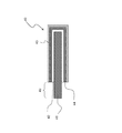
- FIG. 3 is a longitudinal sectional view of the semiconductor element 20 according to the second embodiment of the present invention.
- the first conductivity type semiconductor shell 22 is formed on the entire side surface of the rod-shaped first conductivity type semiconductor core 21 (the outer periphery of the rod-shaped first conductivity type semiconductor core 21. Covering the entire surface) and one end.
- the second conductivity type semiconductor shell 23 covers the entire side surface of the first conductivity type semiconductor shell 22 (the entire outer peripheral surface of the first conductivity type semiconductor shell 22) and one end.
- the semiconductor element 20 is different from the semiconductor element 10 of the first embodiment shown in FIGS. 1 and 2 in that the second conductive type semiconductor shell 23 is other than the other end of the surface of the first conductive type semiconductor shell 22. It covers all of the part. Therefore, when an electrode is to be connected to the first conductivity type semiconductor core 21, the other end of the semiconductor element 20 (on the left side of the semiconductor element 20 in FIG. 3) is exposed to the exposed portion of the first conductivity type semiconductor core 21. It is necessary to connect an electrode or to remove a part of the second conductivity type semiconductor shell 23 to expose the first conductivity type semiconductor shell 22 and to connect the electrode to the exposed portion. Specific materials, sizes, applications, effects obtained, and the like constituting the semiconductor element 20 are the same as those of the semiconductor element 10 of the first embodiment.
- FIG. 4 is a cross-sectional view in the longitudinal direction of the semiconductor element 30 according to the third embodiment of the present invention.
- a side surface and one end of a rod-shaped core 31 are covered with a first conductivity type semiconductor shell 32. Further, the surface of the first conductivity type semiconductor shell 32 is covered with the second conductivity type semiconductor shell 33.
- the semiconductor element 30 is different from the semiconductor element 10 of the first embodiment shown in FIGS. 1 and 2 in that the material of the rod-shaped core 31 and the first conductivity type semiconductor shell 32 is different.
- the crystal defect density of the first conductivity type semiconductor shell 32 is preferably smaller than the crystal defect density of the rod-shaped core 31. Accordingly, the function as the core of the rod-shaped semiconductor element and the function as one side of the PN junction can be shared by the rod-shaped core and the first conductivity type semiconductor shell. Therefore, while maintaining the characteristics of the PN junction composed of the first conductive type semiconductor shell and the second conductive type semiconductor shell, the other characteristics of the rod-shaped semiconductor element are improved at the same time, or Manufacturing costs can be reduced.
- the characteristics of the PN junction for example, when a semiconductor element is used as a photoelectric conversion element, the conversion efficiency is improved, and when the semiconductor element is used as a light emitting diode, the light emission efficiency is improved. Examples of characteristics that can be improved together with the characteristics of the PN junction and the reason why the manufacturing cost can be reduced will be described later.
- the material of the rod-shaped core 31 and the first conductivity type semiconductor shell 32 for example, GaN is selected as the material of the rod-shaped core 31, and n-type silicon is selected as the material of the first conductivity type semiconductor shell 32. Can do. In this case, p-type silicon may be used for the second conductivity type semiconductor shell 33. In this case, because the Young's modulus of the rod-shaped core 31 is larger than that of the first conductivity type semiconductor shell, it is possible to obtain good PN characteristics while improving the rigidity of the semiconductor element 30.
- the semiconductor element when the semiconductor element is separated from the grown substrate and arranged on another substrate, the semiconductor element may bend due to the surface tension of the liquid when the semiconductor element immersed in the liquid is dried.
- the above configuration is effective in such a case.
- the material of the rod-shaped core 31 and the material of the first conductive type semiconductor shell 32 for example, sapphire is used as the material of the rod-shaped core 31 and n is used as the material of the first conductive type semiconductor shell 32.
- a type of gallium nitride can be selected.
- p-type gallium nitride can be selected for the second conductivity type semiconductor shell 33.
- the rod-shaped core can be made from expensive gallium nitride to cheaper sapphire, the manufacturing cost can be reduced while maintaining good PN characteristics.
- an undoped gallium nitride grown by HVPE (Hydride Vapor Phase Epitaxy) method as the material of the rod-shaped core 31
- HVPE Hadride Vapor Phase Epitaxy
- n-type gallium nitride having a low crystal defect can be selected.
- p-type gallium nitride can be used for the second conductivity type semiconductor shell 33.
- the rod-shaped core 31 is formed by the HVPE method that can grow at a relatively high speed although there are many crystal defects, and the first conductivity type semiconductor shell 32 is an n-type gallium nitride having a low crystal defect. This is because the manufacturing cost can be reduced while maintaining good PN characteristics.
- the rod-shaped core 31 is not the first conductivity type semiconductor core.
- the rod-shaped core is composed of the first conductivity type semiconductor core, and the first The conductive type semiconductor shell is made of a material different from that of the first conductive type semiconductor core, and the crystal defect density of the first conductive type semiconductor shell is higher than the crystal defect density of the first conductive type semiconductor core. May be configured to be smaller.
- FIG. 5 is a longitudinal sectional view of a semiconductor device 40 according to the fourth embodiment of the present invention.
- the side surface and one end of a rod-shaped first conductivity type semiconductor core 41 are covered with a first conductivity type semiconductor shell 42.
- the light emitting layer 44 covers the surface of the first conductivity type semiconductor shell 42. Further, the surface of the light emitting layer 44 is covered with a second conductivity type semiconductor shell 43.
- the first conductivity type semiconductor shell 42, the light emitting layer 44 and the second conductivity type semiconductor shell 43 do not cover the entire surface of the first conductivity type semiconductor core 41, and the first conductivity type semiconductor shell 42, light emission
- the layer 44 and the second conductivity type semiconductor shell 43 are configured not to cover the other end portion 49 of the rod-shaped first conductivity type semiconductor core 41.
- the semiconductor element 40 functions as a light emitting diode.
- the semiconductor element 40 is different from the semiconductor element 10 of the first embodiment shown in FIGS. 1 and 2 in that the first conductivity type semiconductor shell 42 covers the entire side surface of the rod-shaped first conductivity type semiconductor core 41.
- the light emitting layer 44 is formed between the first conductive type semiconductor shell 42 and the second conductive type semiconductor shell 43.
- the impurity concentration giving the conductivity type is preferably larger than the impurity concentration giving the conductivity type in the first conductivity type semiconductor shell 42.
- the resistivity of the rod-shaped first conductivity type semiconductor core 41 is preferably smaller than the resistivity of the first conductivity type semiconductor shell 42. If it does so, while the crystallinity of the light emitting layer 44 formed on the rod-shaped 1st conductivity type semiconductor core 41 can be improved, luminous efficiency can be improved, and also the rod-shaped 1st conductivity type semiconductor core 41. This is because the resistance of the light emitting layer 44 can be made sufficiently small to emit light uniformly over the entire surface of the light emitting layer 44.
- the band gap of the material constituting the rod-shaped first conductivity type semiconductor core 41 is preferably larger than the band gap of the material constituting the light emitting layer 44.
- the rod-shaped first conductivity type semiconductor core 41 can be made of n-type GaN, and the light emitting layer 44 can be made of InGaN.
- the first conductivity type semiconductor shell 42 and the second conductivity type semiconductor shell 43 may be n-type GaN and p-type GaN, respectively.
- a rod-shaped core made of sapphire or the like may be used. Even in this case, the band gap of sapphire is larger than the band gap of the light emitting layer made of InGaN.
- a transparent electrode such as ITO (Indium Tin Oxide) on the surface of the second conductivity type semiconductor shell 43.
- ITO Indium Tin Oxide
- the same potential can be applied to the entire surface of the second conductivity type semiconductor shell 43, so that the light emission unevenness can be reduced and the light emission efficiency can be improved, and the emitted light passes through the electrode for the time being. This is because light can be extracted efficiently.
- 6 to 14 are diagrams for explaining an example of the method of manufacturing the semiconductor element according to the fourth embodiment, and show an example of a procedure for forming the semiconductor element.
- the core material or the number of shell formations is changed in the following procedure. Thus, it can be formed similarly.
- a procedure for forming a semiconductor element made of gallium nitride is shown, but a semiconductor element made of another material can be formed by the same procedure.
- a sapphire substrate 61 is prepared.
- a silicon oxide film 62 provided with an opening is formed on the sapphire substrate 61.
- a silicon oxide film 62 having a thickness of, for example, 1 ⁇ m is formed on the sapphire substrate 61 by a CVD (Chemical Vapor Deposition) method, and then, for example, 1 ⁇ m is formed on the silicon oxide film 62 by a photolithography process.
- the opening having a size is patterned so that a part of the surface of the sapphire substrate 61 is exposed.
- metal catalyst particles 63 made of nickel are formed in the openings of the silicon oxide film 62 and in the portions where the sapphire substrate 61 is exposed.
- nickel having a thickness of 3 nm is formed by sputtering on the entire surface of the sapphire substrate 61 on which the patterned silicon oxide film 62 is formed, and annealed at a temperature of about 900 ° C. , Make the nickel agglomerate.
- the growth temperature is set to a temperature of about 850 ° C.
- trimethylgallium (TMG) and ammonia (NH 3 ) are used as the growth gas
- silane (SiH 4 ) is used for supplying n-type impurities
- hydrogen By supplying H 2 ), an n-type GaN semiconductor core having Si as an impurity can be grown.
- the sapphire substrate 61 on which the rod-shaped first conductivity type semiconductor core 64 made of n-type GaN is grown is annealed at a temperature higher than the temperature at which the rod-shaped first conductivity type semiconductor core 64 made of n-type GaN is grown. It is preferable to process.
- the annealing temperature for example, a temperature higher than 850 ° C. and not higher than 1200 ° C. can be adopted.
- the crystal defects of the rod-shaped first conductivity type semiconductor core 64 made of n-type GaN can be recovered, and the crystallinity of the first conductivity type semiconductor core 64 can be improved. Therefore, it is possible to further improve the crystallinity of the first conductivity type semiconductor shell 65 made of an n-type GaN film formed in the first shell formation step performed later.
- the first conductive type semiconductor shell made of an n-type GaN film with a thickness of 200 nm, for example. 65 is formed (first shell forming step).
- the first conductivity type semiconductor shell 65 made of the n-type GaN film can be formed at 900 ° C., for example, using an MOCVD apparatus.
- This n-type GaN film may be formed on the silicon oxide film 62, and later, if necessary, the n-type GaN film on the silicon oxide film 62 may be removed by anisotropic dry etching. good.
- the first conductive semiconductor shell 65 made of the n-type GaN film is formed again on the side surface and the upper surface of the rod-shaped first conductive semiconductor core 64 made of the n-type GaN, thereby obtaining uniform and crystalline properties. A good n-type GaN crystal can be exposed on the surface.
- a light emitting layer 66 made of an InGaN film for example, with a thickness of 5 nm is formed on the side surface and the upper surface of the first conductivity type semiconductor shell 65 made of an n-type GaN film.
- the light emitting layer 66 made of this InGaN film is formed using a MOCVD apparatus, for example, with a growth temperature set at about 750 ° C., using TMG, NH 3 and trimethylindium (TMI) as growth gases, and H 2 as a carrier gas. Can be grown by feeding.
- the light emitting layer 66 made of this InGaN film may have a multiple quantum well structure (MQW) by stacking a plurality of GaN films or AlGaN films as block layers.
- This InGaN film may be formed on the silicon oxide film 62, or the InGaN film on the silicon oxide film 62 may be removed later by anisotropic dry etching if necessary.
- a second conductivity type semiconductor shell 67 made of a p-type GaN film with a thickness of, for example, 100 nm is formed on the side surface and upper surface of the light emitting layer 66 made of InGaN film (second Shell forming step).
- the second conductivity type semiconductor shell 67 made of the p-type GaN film is set to a growth temperature of, for example, about 800 ° C. using a MOCVD apparatus, TMG and NH 3 are used as growth gases, and p-type impurities are used as p-type impurities.
- TMG and NH 3 are used as growth gases
- p-type impurities are used as p-type impurities.
- the silicon oxide film 62 is removed by wet etching with hydrofluoric acid (HF). Thereby, a part of the first conductivity type semiconductor shell 65 made of the n-type GaN film is exposed.
- HF hydrofluoric acid
- the sapphire substrate 61 and the rod-shaped structure formed on the surface thereof are immersed in a liquid such as water and irradiated with ultrasonic waves, thereby removing the rod-shaped structure from the substrate.
- Disconnect semiconductor element isolation step. In this way, the separated individual rod-shaped structure, that is, the semiconductor element 60 having the function of a light emitting diode is manufactured.
- n-type silicon can be grown as a rod-shaped first conductive type semiconductor core and first conductive type semiconductor shell, and p-type silicon can be grown as a second conductive type semiconductor shell without forming a light emitting layer.
- a semiconductor element having a function of a photoelectric conversion element can be formed.
- the core-forming step of forming the rod-shaped core 64 on the substrate 61 and the rod-shaped core 64 are formed and then covered with the first conductivity type semiconductor shell 65.
- a first shell forming step and a second shell forming step of forming a first conductive type shell 65 and then covering the first conductive type shell 65 with a second conductive type semiconductor shell 67 are provided.
- the first conductivity type semiconductor shell 65 is formed after the rod-shaped semiconductor core 64 is formed, the first conductivity type semiconductor having a uniform and good crystallinity is formed on the surface of the first conductivity type semiconductor shell 65. Exposed. Therefore, the crystallinity of the light emitting layer 66 formed on the first conductivity type semiconductor shell 67 can be improved.
- the first conductive type semiconductor shell is exposed on the surface of the first conductive type semiconductor shell, so that the first conductive type semiconductor shell is then exposed.
- a PN junction having good characteristics can be obtained by the second conductive type semiconductor shell formed to cover the first conductive type semiconductor shell.
- the rod-shaped core 64 is formed separately from the first conductivity type semiconductor shell 65 prior to the formation of the first conductivity type semiconductor shell 65, the first conductivity type semiconductor shell 65 and Can be formed independently. Therefore, the core 64 of the rod-shaped semiconductor element can be formed to have a property suitable for fulfilling the function as the core of the rod-shaped semiconductor element.
- the function as the core of the rod-shaped semiconductor element and the function as one side of the PN junction can be shared by the first conductivity type semiconductor core 64 and the first conductivity type semiconductor shell 65. Therefore, it is possible to improve other characteristics of the rod-shaped semiconductor element while maintaining the characteristics of the PN junction constituted by the first conductivity type semiconductor shell 65 and the second conductivity type semiconductor shell 67 well. In addition, the manufacturing cost can be reduced.
- the characteristics of the PN junction for example, when a semiconductor element is used as a photoelectric conversion element, the conversion efficiency is improved, and when the semiconductor element is used as a light emitting diode, the light emission efficiency is improved.
- the core forming step is performed by growing a rod-shaped core 64 on the substrate 61.
- the substrate 61 and the rod-shaped core 64 are in contact with each other in the same area as the cross-sectional area of the rod-shaped core 64. Since the diameter of the rod-shaped core 64 is from nanoscale to microscale and the cross-sectional area is small, the rod-shaped core 64 can be formed on the substrate 61 with high density.
- the rod-shaped cores 64 are discretely formed on the substrate 61. Therefore, warpage of the substrate 61 due to a mismatch between the lattice constants of the material constituting the substrate 61 and the material constituting the rod-shaped core 64 can be suppressed. Therefore, the accuracy of the photolithography process in the process of forming the semiconductor element can be improved, and the yield of the semiconductor element can be easily improved.
- the annealing process is performed at a temperature higher than the temperature for forming the core 64.
- the crystal defects of the core 64 can be improved by recovering the crystal defects of the core 64. Therefore, the crystallinity of the second conductivity type semiconductor shell 67 and the light emitting layer 66 formed thereafter can be further improved.
- the impurity concentration of the semiconductor core 64 which gives conductivity type to the rod-shaped first conductivity type semiconductor core 64 made of n-type GaN is the semiconductor which gives conductivity type to the first conductivity type semiconductor shell 65 made of n-type GaN film.
- the impurity concentration of the shell 65 is preferably larger.
- the resistivity of the rod-shaped first conductivity type semiconductor core 64 made of n-type GaN is preferably smaller than the resistivity of the first conductivity type semiconductor shell 65 made of an n-type GaN film.
- the crystallinity of the light emitting layer 66 made of the InGaN film formed on the first conductivity type semiconductor shell 65 made of the n-type GaN film can be improved, and the light emission efficiency can be improved. This is because the resistance of the rod-shaped first conductivity type semiconductor core 64 made of n-type GaN can be sufficiently reduced.
- the band gap of the material constituting the rod-shaped first conductivity type semiconductor core 64 is preferably larger than the band gap of the material constituting the light emitting layer 66.
- the rod-shaped first conductivity type semiconductor core 64 is made of n-type GaN
- the light emitting layer 66 is made of InGaN.
- 15 to 17 are diagrams for explaining other procedures for manufacturing the semiconductor device of the fourth embodiment.
- This modification is different from the procedure shown in FIGS. 6 to 14 only in that metal catalyst particles are not used when growing a rod-shaped first conductivity type semiconductor core.
- the description of the procedure similar to the above method is omitted in principle.
- a silicon oxide film 72 provided with an opening is formed on a sapphire substrate 71. This is exactly the same as the procedure described in FIG.
- n-type GaN having a length of 10 ⁇ m is grown on the exposed sapphire substrate 71 corresponding to the opening of the silicon oxide film 72 using a MOCVD apparatus.
- a rod-shaped first conductive type semiconductor core 74 is formed (core forming step).
- metal catalyst grains are not used, crystal growth needs to be performed at a relatively high temperature of about 1050 ° C.
- the rod-shaped first conductivity type semiconductor core 74 made of n-type GaN for example, the first conductivity type semiconductor made of an n-type GaN film with a thickness of 200 nm.
- the shell 75 is formed (first shell forming step).
- the metal catalyst particles are not used when growing the rod-shaped first conductivity type semiconductor core 74, so that there is no metal contamination and the rod-shaped first conductivity type semiconductor core 74 can be improved. . Accordingly, it is possible to further improve the crystallinity of the first conductive type semiconductor shell 75 and the second conductive type semiconductor shell formed on the rod-shaped first conductive type semiconductor core 74.
- FIG. 18 is a longitudinal sectional view of a semiconductor device 50 according to a fifth embodiment of the present invention.
- the semiconductor element 50 As shown in FIG. 18, in the semiconductor element 50, the side surface and one end of the rod-shaped first conductivity type semiconductor core 51 are covered with the first conductivity type semiconductor shell 52.
- the light emitting layer 54 covers the surface of the first conductivity type semiconductor shell 52. Further, the surface of the light emitting layer 54 is covered with a second conductivity type semiconductor shell 53.
- the semiconductor element 50 is different from the semiconductor element 40 shown in FIG. 5 in that the first conductive type semiconductor shell 52, the light emitting layer 54 and the second conductive type semiconductor shell 53 are different from the first conductive type semiconductor shell 52. It covers all surfaces except the end face of the end. Therefore, when an electrode is to be connected to the first conductivity type semiconductor core 51, the other end of the semiconductor element 50 (on the left side of the semiconductor element 50 in FIG.
- FIGS. 19 to 23 are views for explaining an example of a method for manufacturing the semiconductor element (see FIG. 18) of the fifth embodiment, and are diagrams showing an example of a procedure for forming the semiconductor element.
- the semiconductor element (refer FIG. 3) of 2nd Embodiment can be formed by the method similar to the method demonstrated below by changing the formation frequency of a shell in the method demonstrated below.
- a procedure for forming a semiconductor element made of gallium nitride is shown as an example, but a semiconductor element made of another material can also be formed by a procedure similar to the procedure described below.
- an n-type GaN film 82 is formed on the surface of the sapphire substrate 81.
- the n-type GaN film 82 can be formed by, for example, an MOCVD apparatus, and can be formed to a thickness of 10 ⁇ m, for example.
- a silicon oxide film is deposited on the n-type GaN film 82 and patterned by a photolithography process to form a hard mask 83 made of a silicon oxide film.
- the silicon oxide film can be deposited with a thickness of 1 ⁇ m by, for example, a CVD method, and the hard mask 83 made of the silicon oxide film has a circular shape with a diameter of 1 ⁇ m, for example, in a cross section perpendicular to the thickness direction. It can be composed of triangles, squares, hexagons, and the like.
- the n-type GaN film is etched by anisotropic dry etching using the hard mask 83 made of a silicon oxide film as a mask, and a rod-shaped first conductivity type made of n-type GaN.
- the semiconductor core 84 is formed (core formation step).
- the shape of the hard mask 83 made of a silicon oxide film the cross-sectional shape of the rod-shaped first conductivity type semiconductor core 84 can be freely changed. Therefore, for example, if the surface of the n-type GaN film 82 is grown so as to be a c-plane, the hard mask 83 made of a silicon oxide film is formed into a triangle, so that a rod-shaped first conductivity type semiconductor core 84 is formed. All the side surfaces can be nonpolar surfaces (a-plane and m-plane).
- the annealing temperature can be 700 ° C. to 1200 ° C., for example.
- the crystal defects of the rod-shaped first conductivity type semiconductor core 84 made of n-type GaN can be recovered and the crystallinity of the semiconductor core 84 can be improved. Therefore, it is possible to further improve the crystallinity of the first conductivity type semiconductor shell made of the n-type GaN film formed in the first shell formation step performed later.
- a sapphire substrate 81 on which a rod-shaped first-conductivity-type semiconductor core 84 made of n-type GaN is formed is immersed in, for example, hot phosphoric acid at 150 ° C., and a crystal defect layer generated by etching in the core forming step is removed. It can be selectively removed. Also in this case, the crystal defects of the semiconductor core 84 can be improved by recovering the crystal defects of the rod-shaped first conductivity type semiconductor core 84 made of n-type GaN. Therefore, it is possible to further improve the crystallinity of the first conductivity type semiconductor shell made of the n-type GaN film formed in the first shell formation step performed later.
- the first conductive semiconductor shell made of n-type GaN film with a thickness of, for example, 200 nm is formed on the side surface and upper surface of the rod-shaped first conductive semiconductor core 84 made of n-type GaN. 85 is formed (first shell forming step). As described above, the first conductive semiconductor shell 85 made of the n-type GaN film is formed again on the side surface and the upper surface of the rod-shaped first conductive semiconductor core 84 made of the n-type GaN, thereby obtaining uniform and crystalline properties. A good n-type GaN crystal can be exposed on the surface.
- the rod-shaped first-conductivity-type semiconductor core 84 made of n-type GaN is formed by etching, and thus is damaged by etching. Therefore, by forming the first conductivity type semiconductor shell 85 made of the n-type GaN film, the effect of reducing crystal defects on the surface of the first conductivity type semiconductor is increased.
- a light emitting layer 86 made of an InGaN film is formed with a thickness of, for example, 5 nm on the side surface and the upper surface of the first conductivity type semiconductor shell 85 made of an n-type GaN film.
- a second conductivity type semiconductor shell 87 made of a p-type GaN film is formed to a thickness of, for example, 100 nm on a side surface and an upper surface of the light emitting layer 86 made of an InGaN film (second shell forming step).
- the formation conditions of the rod-shaped first conductive type semiconductor core 84, the light emitting layer 86 made of InGaN film, and the second conductive type semiconductor shell 87 made of p-type GaN film are the same as those in the procedure for forming the semiconductor device of the fourth embodiment. It may be the same as that.
- the rod-shaped structure is separated from the substrate by immersing the sapphire substrate 81 and the rod-shaped structure formed on the surface thereof in a liquid such as water and irradiating ultrasonic waves ( Semiconductor element separation step).
- a liquid such as water and irradiating ultrasonic waves
- n-type silicon can be grown as the rod-shaped first conductive type semiconductor core and the first conductive type semiconductor shell, and p-type silicon can be grown as the second conductive type semiconductor shell without forming the light emitting layer.
- a semiconductor element having a function of a photoelectric conversion element can be formed.
- the core forming step of forming the rod-shaped core 84 on the substrate 81, and the first-conductivity-type semiconductor shell 85 after the rod-shaped core 84 is formed Forming a first shell covering the first conductive type shell 85 and forming a second shell covering the first conductive type shell 85 directly or indirectly with the second conductive type semiconductor shell 87. Process.
- the first conductive type semiconductor shell 85 is formed after the rod-shaped semiconductor core 84 is formed by such a method, the surface of the first conductive type semiconductor shell 85 is uniform and has good crystallinity.
- the first conductivity type semiconductor can be exposed. Therefore, the crystallinity of the light emitting layer 86 formed on the first conductivity type semiconductor shell 85 can be improved.
- the uniform and highly crystalline first conductive type semiconductor is exposed on the surface of the first conductive type semiconductor shell. Can do. Accordingly, when the light emitting layer is not formed on the first conductivity type semiconductor shell, the first conductivity type semiconductor shell and the second conductivity type semiconductor shell formed so as to cover the first conductivity type semiconductor shell. Thus, a PN junction having good characteristics can be obtained.
- the rod-shaped semiconductor element core is suitable for functioning as a core of the rod-shaped semiconductor element. Can be formed. Therefore, the function as the core of the rod-shaped semiconductor element and the function as one side of the PN junction can be shared by the first conductivity type semiconductor core and the first conductivity type semiconductor shell. Therefore, it is possible to improve other characteristics of the rod-shaped semiconductor element while maintaining the characteristics of the PN junction composed of the first conductive type semiconductor shell and the second conductive type semiconductor shell, or to improve the manufacturing process. Costs can be reduced. Therefore, by improving the characteristics of the PN junction, for example, when a semiconductor element is used as a photoelectric conversion element, the conversion efficiency is improved, and when the semiconductor element is used as a light emitting diode, the light emission efficiency is improved.
- the core forming step is performed by etching a part of the substrate surface made of the material constituting the core.
- the cross-sectional shape of the rod-shaped core can be freely changed by photolithography. Therefore, for example, the crystal orientation of the side surface of the rod-shaped core can be made favorable, and the characteristics of the semiconductor element can be improved.
- the crystal defect of a rod-shaped core can be recovered and crystallinity can be improved. Therefore, it is possible to further improve the crystallinity of the first conductivity type semiconductor shell to be formed in the first shell formation step performed later.
- a part of the core formed in the core forming step is removed by wet etching after the core forming step and before the first shell forming step. This is also because the crystal defects of the rod-shaped core can be improved by recovering the crystal defects of the rod-shaped core. Therefore, it is possible to further improve the crystallinity of the first conductivity type semiconductor shell to be formed in the first shell formation step performed later.
- the crystal defects of the rod-shaped core can be improved by recovering the crystal defects of the rod-shaped core, so that the crystallinity of the second conductivity type semiconductor shell and the light emitting layer formed thereafter can be further improved.
- the impurity concentration of the semiconductor core 84 that gives conductivity to the rod-shaped first conductivity type semiconductor core 84 made of n-type GaN is the semiconductor that gives conductivity to the first conductivity type semiconductor shell 85 made of n-type GaN film.
- the impurity concentration of the shell 85 is preferably larger.
- the resistivity of the rod-shaped first conductivity type semiconductor core 84 made of n-type GaN is preferably smaller than the resistivity of the first conductivity type semiconductor shell 85 made of an n-type GaN film.
- the crystallinity of the light emitting layer 86 made of the InGaN film formed on the first conductivity type semiconductor shell 85 made of the n-type GaN film is improved, the light emission efficiency is improved, and the rod-like shape made of the n-type GaN is improved. This is because the resistance of the first conductivity type semiconductor core 84 can be sufficiently reduced.
- the band gap of the material constituting the rod-shaped first conductivity type semiconductor core 84 is preferably larger than the band gap of the material constituting the light emitting layer 86.
- the rod-shaped first conductivity type semiconductor core 84 is made of n-type GaN
- the light emitting layer 86 is made of InGaN.
- FIG. 24 is a cross-sectional view of the solar cell according to the sixth embodiment of the present invention.
- This solar cell includes a plurality of semiconductor elements 150 according to an embodiment of the present invention.
- an n-type silicon layer 102 serving as a lower electrode is formed on a sapphire substrate 101.
- a silicon oxide film 103 having an opening is formed on the n-type silicon layer 102.
- Part of the first conductivity type semiconductor core 104 made of rod-shaped n-type silicon is filled in the opening.
- the semiconductor core 104 stands upright from the opening.
- the semiconductor core 104 is electrically connected to the n-type silicon layer 102 serving as a lower electrode.
- a first conductivity type semiconductor shell 105 made of an n-type silicon film and a second conductivity type semiconductor shell 106 made of a p-type silicon film are provided on the side and top surfaces of the first conductivity type semiconductor core 104 made of n-type silicon.
- a first conductivity type semiconductor shell 105 made of an n-type silicon film and a second conductivity type semiconductor shell 106 made of a p-type silicon film are provided on the side and top surfaces of the first conductivity type semiconductor core 104 made of n-type silicon.
- a second conductivity type semiconductor shell 106 made of a p-type silicon film are provided on the side and top surfaces of the first conductivity type semiconductor core 104 made of n-type silicon.
- the first conductive semiconductor core 104 made of rod-shaped n-type silicon, the first conductive semiconductor shell 105 made of n-type silicon film, and the second conductive semiconductor shell 106 made of p-type silicon film, photoelectric conversion
- a semiconductor element 150 having an element function is formed.
- the plurality of semiconductor elements 150 are discretely formed on the sapphire substrate 101, and transparent electrodes 107 made of ITO are filled in the gaps and above the plurality of semiconductor elements 150. Further, a metal electrode 109 serving as an upper electrode is formed on a part of the transparent electrode 107.
- the diameter of the first conductivity type semiconductor core 104 made of rod-shaped n-type silicon can be set to, for example, 500 nm.
- the thickness of the first conductivity type semiconductor shell 105 made of an n-type silicon film can be set to 200 nm, for example.
- the thickness of the second conductivity type semiconductor shell 106 made of a p-type silicon film can be set to 200 nm, for example.
- the concentration of phosphorus atoms that give n-type to the first conductivity type semiconductor core 104 made of rod-shaped n-type silicon can be, for example, 1 ⁇ 10 19 cm ⁇ 3 . Further, the concentration of phosphorus atoms that give the n-type to the first conductivity type semiconductor shell 105 made of an n-type silicon film can be, for example, 1 ⁇ 10 17 cm ⁇ 3 .
- the resistivity of the first conductivity type semiconductor core 104 made of rod-shaped n-type silicon is 6 ⁇ 10 ⁇ 3 ⁇ cm, and the resistivity of the first conductivity type semiconductor shell 105 made of n-type silicon film. Is 9 ⁇ 10 ⁇ 2 ⁇ cm.
- the crystal defect density of the first conductivity type semiconductor shell 105 made of the n-type silicon film is smaller than the crystal defect density of the first conductivity type semiconductor core 104 made of rod-shaped n-type silicon. Therefore, this solar cell has excellent electrical characteristics of a PN junction composed of the first conductivity type semiconductor shell 105 made of n-type silicon film and the second conductivity type semiconductor shell 106 made of p-type silicon film. Therefore, the electrical resistance of the first conductivity type semiconductor core 104 made of rod-shaped n-type silicon can be reduced, and the conversion efficiency of the solar cell can be improved.
- FIGS. 25 to 28 are diagrams for explaining an example of the method for manufacturing the solar cell according to the sixth embodiment, and show an example of a procedure for forming the solar cell.
- a sapphire substrate 101 is prepared.
- an n-type silicon layer (film) 102 is epitaxially grown on the sapphire substrate 101 to a thickness of, for example, 200 nm by the CVD method.
- a silicon oxide film 103 having an opening is formed on an n-type silicon layer 102, and a rod-shaped first conductivity type semiconductor core 104 made of n-type silicon is formed by a CVD method.
- a CVD method To grow from the opening (core growth step).
- catalytic metal particles made of gold may be formed in the opening in order to promote growth.
- first conductive type semiconductor shell 105 made of n-type silicon is formed on the side surface and upper surface of the rod-shaped first conductive type semiconductor core 104 made of n-type silicon (first shell forming step).
- second conductivity type semiconductor shell 106 made of p type silicon is formed on the side surface and upper surface of the first conductivity type semiconductor shell 105 made of n type silicon (second shell formation step).
- a first conductive type semiconductor core 104 made of rod-shaped n-type silicon
- a first conductive type semiconductor shell 105 made of n-type silicon film
- a second conductive type semiconductor shell 106 made of p-type silicon film.
- a semiconductor element 150 having a function of a photoelectric conversion element is configured.
- a transparent electrode 107 made of an ITO layer is formed by sputtering or CVD so as to fill between and above the plurality of semiconductor elements 150. Then, the metal layer is patterned on the transparent electrode 107 to form the metal electrode 109 to be the upper electrode, and the solar cell 100 is completed.
- the solar cell of this embodiment includes the semiconductor element 150 of one embodiment of the present invention that has the function of a photoelectric conversion element. Therefore, the conversion efficiency of the solar cell can be improved.
- FIG. 29 is a cross-sectional view of a light emitting diode according to a seventh embodiment of the present invention.
- This light emitting diode includes a plurality of semiconductor elements 250 according to an embodiment of the present invention.
- an n-type GaN layer 202 serving as a lower electrode is formed on a sapphire substrate 201. Further, a silicon oxide film 203 having an opening is formed on the n-type GaN layer 202. Part of the first conductivity type semiconductor core 204 made of rod-shaped n-type GaN is filled in the opening. The semiconductor core 204 stands upright from the opening. The semiconductor core 204 is electrically connected to the n-type GaN layer 202 serving as a lower electrode.
- first conductivity type semiconductor core 204 made of rod-shaped n-type GaN
- first conductivity type semiconductor shell 205 made of n-type GaN film
- light emitting layer 210 made of InGaN film
- p-type GaN A second conductivity type semiconductor shell 206 made of a film is laminated in this order.
- the semiconductor shell 205, the light emitting layer 210, and the semiconductor shell 206 cover the side surface and the upper surface of the semiconductor core 204.
- the semiconductor shell 206 constitutes a semiconductor element 250 having a function of a photoelectric conversion element.
- the plurality of semiconductor elements 250 are discretely formed on the sapphire substrate 201, and transparent electrodes 207 made of ITO are filled in the gaps and above the plurality of semiconductor elements 250. Further, a metal electrode 209 serving as an upper electrode is formed on a part of the transparent electrode 207.
- the diameter of the first conductivity type semiconductor core 204 made of rod-shaped n-type GaN can be set to 1 ⁇ m, for example.
- the thickness of the first conductivity type semiconductor shell 205 made of an n-type GaN film can be set to 400 nm, for example.
- the thickness of the light emitting layer 210 made of an InGaN film can be set to 5 nm, for example.
- the thickness of the second conductivity type semiconductor shell 206 made of a p-type GaN film can be set to 200 nm, for example.
- the concentration of silicon atoms giving n-type to the first conductivity type semiconductor core 204 made of rod-shaped n-type GaN can be set to 1 ⁇ 10 19 cm ⁇ 3 , for example. Further, the concentration of silicon atoms that give n-type to the first conductivity type semiconductor shell 205 made of the n-type GaN film can be set to 1 ⁇ 10 17 cm ⁇ 3 , for example.
- the resistivity of the first conductivity type semiconductor core 204 made of rod-shaped n-type GaN is about 2 ⁇ 10 ⁇ 3 ⁇ cm
- the resistivity of the first conductivity type semiconductor shell 205 made of n-type GaN film is about 3 ⁇ 10 ⁇ 1 ⁇ cm.
- the crystal defect density of the first conductivity type semiconductor shell 205 made of the n-type GaN film is smaller than the crystal defect density of the first conductivity type semiconductor core 204 made of the rod-like n-type GaN. Therefore, the electrical characteristics of the PN junction composed of the first conductivity type semiconductor shell 205 made of the n-type GaN film and the second conductivity type semiconductor shell 206 made of the p-type GaN film can be kept good.
- the electrical resistance of the first conductivity type semiconductor core 204 made of rod-shaped n-type GaN can be reduced, and the light emission efficiency of the light emitting diode can be improved.
- the light emitting diode of this embodiment includes the semiconductor element 250 of one embodiment of the present invention having the function of a light emitting diode. Therefore, the light emission efficiency of the light emitting diode can be improved.
- FIG. 30 is a schematic cross-sectional view of a light emitting diode according to an eighth embodiment of the present invention.
- This light-emitting diode includes a plurality of semiconductor elements 350A and 350B according to an embodiment of the present invention. Specifically, in the light emitting diode 300, a plurality of light emitting diode elements 350A and 350B are disposed on a glass substrate 311. The shape of the end of the light emitting diode element 350A is slightly different from the shape of the end of the light emitting diode element 350B. This is because two directions are allowed when the light emitting diode element is arranged on the glass substrate 311. However, this difference does not affect the operation of the light emitting diode of this embodiment.
- Each of the light emitting diode elements 350A and 350B includes a first conductive type semiconductor core 304 made of rod-shaped n-type GaN, a first conductive type semiconductor shell 305 made of an n-type GaN film, a light emitting layer 310 made of an InGaN film, and p.
- membrane is comprised.
- the diameter of the first conductivity type semiconductor core 304 made of rod-shaped n-type GaN can be set to 1 ⁇ m, for example.
- the thickness of the first conductivity type semiconductor shell 305 made of an n-type GaN film can be set to 400 nm, for example.
- the thickness of the light emitting layer 310 made of the InGaN film can be set to 5 nm, for example.
- the thickness of the second conductivity type semiconductor shell 306 made of a p-type GaN film can be set to 200 nm, for example.
- the concentration of silicon atoms that give n-type to the first conductivity type semiconductor core 304 made of rod-shaped n-type GaN can be set to 1 ⁇ 10 19 cm ⁇ 3 , for example. Further, the concentration of silicon atoms that give the n-type to the first conductivity type semiconductor shell 305 made of the n-type GaN film can be, for example, 1 ⁇ 10 17 cm ⁇ 3 .
- the resistivity of the first conductivity type semiconductor core 304 made of rod-shaped n-type GaN is about 2 ⁇ 10 ⁇ 2 ⁇ cm
- the resistivity of the first conductivity type semiconductor shell 305 made of an n-type GaN film is about 3 ⁇ 10 ⁇ 1 ⁇ cm.
- the crystal defect density of the first conductivity type semiconductor shell 305 made of the n-type GaN film is smaller than the crystal defect density of the first conductivity type semiconductor core 304 made of the rod-shaped n-type GaN. Therefore, the electrical characteristics of the PN junction composed of the first conductivity type semiconductor shell 305 made of the n-type GaN film and the second conductivity type semiconductor shell 306 made of the p-type GaN film can be kept good.
- the electric resistance of the first conductive type semiconductor core 304 made of rod-shaped n-type GaN can be reduced, and the light emission efficiency of the light emitting diode element can be improved.
- the number of the light emitting diode elements 350A and 350B can be changed according to the required light quantity. If the above-described size is adopted as the size of the light emitting diode element, for example, a preferable amount of light can be obtained by arranging 1,000 to 100,000 light emitting diode elements on one glass substrate.
- a first electrode 312 and a second electrode 313 are formed on the glass substrate 311. This is formed in order to arrange the light emitting diode elements 350A and 350B at predetermined positions on the glass substrate 311 as will be described later.
- An interlayer insulating film 314 made of a silicon oxide film is formed on the glass substrate 311 and the light emitting diode elements 350A and 350B.
- metal wirings 315 and 316 are electrically connected to the light emitting diode elements 350A and 350B through contact holes opened in the interlayer insulating film 314. By applying a voltage between the metal wires 315 and 316, the light emitting diode elements 350A and 350B emit light.
- 31 to 39 are views for explaining an example of the manufacturing method of the light emitting diode according to the eighth embodiment, and show an example of a procedure for forming the light emitting diode.
- the light emitting diode element of the fifth embodiment is formed according to the procedure described with reference to FIGS. Specifically, as described above, the light emitting diode element is formed with a core forming step of forming a plurality of rod-shaped cores on the first substrate, and after forming the plurality of rod-shaped cores, the first conductivity type semiconductor is formed.
- a plurality of rod-shaped semiconductor elements each having a semiconductor shell and a second conductivity type semiconductor shell are formed through a semiconductor element separation step of separating the semiconductor element from the substrate.
- first and second electrodes 312 and 313 are formed on the surface of a glass substrate 311 which is a second substrate different from the first substrate.
- the first and second electrodes 312 and 313 can be formed using photolithography or printing technology.
- pads are formed on the metal electrodes 312 and 313 so that a potential is applied from the outside.
- the previously prepared light emitting diode elements are arranged on the metal electrodes 312, 313 facing each other (semiconductor element arranging step).
- the number of array regions in which the light-emitting diode elements are arrayed is 8 ⁇ 3. However, in actuality, any number of array regions can be used.
- FIG. 32 is a schematic sectional view taken along line XIX-XIX in FIG.
- isopropyl alcohol (IPA) 321 including a light emitting diode element 350 is thinly applied on a glass substrate 311.
- the material to be applied may be ethylene glycol, propylene glycol, methanol, ethanol, or acetone in addition to IPA321, or may be a mixture of two or more of these materials, or IPA and those Of these, a mixture of one or more materials may be used.
- IPA 321 a liquid made of another organic material, water, or the like can be used instead of the IPA 321, a liquid made of another organic material, water, or the like can be used.
- the light emitting diode element 350 is the semiconductor element of the fifth embodiment (see FIG. 6).
- an insulating film of about 10 nm to 30 nm may be coated on the entire surface of the glass substrate 311 so as to cover the metal electrodes 312 and 313.
- the thickness of the IPA 321 that is applied and includes the light emitting diode element 350 is such that the light emitting diode element 350 can move in the liquid so that the light emitting diode element 350 can be arranged in a subsequent step of arranging the light emitting diode element 350. It is. Therefore, the thickness of the applied IPA 321 is equal to or greater than the thickness of the light emitting diode element 350, and can be, for example, several ⁇ m to several mm. If the applied thickness is too thin, the light emitting diode element 350 is difficult to move. Conversely, if it is too thick, the time for drying the liquid becomes long.
- the amount of the light emitting diode element 350 is preferably 1 ⁇ 10 4 cm ⁇ 3 to 1 ⁇ 10 7 cm ⁇ 3 with respect to the amount of IPA.
- a frame is formed on the outer periphery of the metal electrode on which the light emitting diode element 350 is arranged, and the IPA 321 including the light emitting diode element 350 is formed in the frame to have a desired thickness. May be filled.
- the IPA 321 including the light emitting diode element 350 has viscosity, it can be applied to a desired thickness without requiring a frame.
- a potential difference of 1 V is applied between the metal electrodes 312,313.
- the potential difference between the metal electrodes 312 and 313 can be 0.1 to 10V.
- the voltage is 0.1 V or less, the arrangement of the bar light emitting diode elements 350 is deteriorated. Therefore, it is preferably 1 to 5V, and more preferably about 1V.
- FIG. 33 is a diagram for explaining the principle in which the light emitting diode elements 350 are arranged on the metal electrodes 312 and 313.
- a potential VL is applied to the metal electrode 312 and a potential VR (VL ⁇ VR) is applied to the metal electrode 313, a negative charge is induced in the metal electrode 312 and a positive charge is applied to the metal electrode 313. Is induced.
- a positive charge is induced on the side close to the metal electrode 312 and a negative charge is induced on the side close to the metal electrode 313 in the rod-shaped light emitting diode element 350.
- the charge is induced in the light emitting diode element 350 by electrostatic induction.
- the light-emitting diode element 350 placed in the electric field is caused to induce charges on the surface until the internal electric field becomes zero.
- an attractive force is exerted between the electrodes 312, 313 and the light emitting diode element 350 by electrostatic force, and the light emitting diode element 350 is aligned along the lines of electric force generated between the metal electrodes 312, 313,
- the electrodes 312 and 313 are arranged so as to crosslink.
- the electric field in the liquid is gradually weakened due to the induction of electric charges on the insulating film, so that the light-emitting diode element 350 is stably placed on the electrodes 312 and 313. I can't stop it.
- the AC voltage indicative of the V R to indicate Figure 34B the V L in FIG. 34A it is preferable that applied between the metal electrodes 312 and 313.
- a reference potential is applied to the metal electrode 313, and an AC voltage with an amplitude V PPL / 2 is applied to the metal electrode 312.
- the frequency of the AC voltage applied to the metal electrode 312 is preferably 10 Hz to 1 MHz, and more preferably 50 Hz to 1 kHz because the arrangement is most stable.
- the AC voltage applied between the metal electrodes 312 and 313 is not limited to a sine wave, but may be any one that periodically varies, such as a rectangular wave, a triangular wave, and a sawtooth wave.
- V PPL was preferably about 1V.
- the glass substrate 311 is heated to evaporate the liquid and dry the light emitting diode elements 350. Align and fix so as to crosslink.
- FIG. 35 shows a plan view of the glass substrate 311 on which the light emitting diode elements 350 are arranged.
- FIG. 36 shows a cross-sectional view of the glass substrate 311 on which the light emitting diode elements 350 are arranged.
- the light emitting diode element 350A is arranged with the exposed side of the first conductivity type core made of rod-shaped n-type GaN facing the left side, and the light emitting diode element 350B has the exposed side facing the right side. Arranged in the state. This is because two directions are allowed when the light emitting diode element is arranged on the metal electrodes 312 and 313.
- a photoresist 317 is patterned on the glass substrate 311 so that a part of the light emitting diode elements 350A and 350B is exposed. Then, in the opening of the photoresist 317, the light emitting layer 310 made of the InGaN film and the second conductivity type semiconductor shell 306 made of the p-type GaN film are removed by etching. As this etching, dry etching having strong isotropic property is appropriate. Thereafter, the photoresist 317 is removed.
- an interlayer insulating film 314 is applied on the glass substrate 311.
- the interlayer insulating film 314 can be formed, for example, by applying 2 ⁇ m of a silicon oxide film.
- an opening is provided in the interlayer insulating film 314.
- a metal is deposited by sputtering or the like, thereby filling the opening of the interlayer insulating film 314 and forming a metal film on the interlayer insulating film 314.
- the metal film is patterned by photolithography to form metal wirings 315 and 316, and the light emitting diode elements 350A and 350B are wired to complete the light emitting diode 300.
- the light-emitting diode of the present embodiment includes the light-emitting diode elements 350A and 350B of the embodiment of the present invention having the function of a light-emitting diode. Therefore, the light emission efficiency of the light emitting diode can be improved.
- the light emitting diode of the above embodiment includes a substrate 311 different from the substrate of the light emitting diode elements 350A and 350B, and light emitting diode elements 350A and 350B which are semiconductor elements of one embodiment of the present invention disposed on the substrate 311; Wirings 315 and 316 that electrically connect the light emitting diode elements 350A and 350B are provided. Therefore, the arrangement interval of the light emitting diode elements (semiconductor elements having a light emitting diode function) 350A and 350B can be freely set on the substrate 311.
- the light emitting diode elements 350A and 350B which are semiconductor elements having the function of the light emitting diode, can be accurately arranged at predetermined positions, the light emitting diode elements 350A and 350B can be efficiently released to the substrate, The temperature rise of the light emitting diode can be suppressed. Therefore, both the efficiency and reliability of the light emitting diode can be improved.
- the above-described procedure for forming the light-emitting diode includes a core forming step of forming a plurality of rod-shaped cores on a first substrate, and after forming the plurality of rod-shaped cores, a first conductivity type semiconductor shell A first shell forming step of covering, a second shell forming step of forming the first conductivity type shell and then covering with a second conductivity type semiconductor shell, the rod-shaped core, and the first conductivity type semiconductor shell And a semiconductor element separating step of separating a plurality of semiconductor elements each having a second conductivity type semiconductor shell from the substrate, and a semiconductor element arranging step of disposing the plurality of semiconductor elements on the second substrate.
- the semiconductor element is covered with the first conductivity type semiconductor shell and the second conductivity type shell after the rod-shaped core is formed on the first substrate. Therefore, the PN junction area per unit substrate area, that is, the light emitting area can be greatly increased, and the manufacturing cost can be reduced.
- the rod-shaped core is formed by forming the first conductive type semiconductor shell. Therefore, the core of the rod-shaped semiconductor element can be formed so as to have a property suitable for functioning as the core of the rod-shaped semiconductor element. Therefore, other characteristics of the rod-shaped semiconductor element can be improved while maintaining the characteristics of the PN junction constituted by the first conductivity type semiconductor shell and the second conductivity type semiconductor shell.
- the arrangement interval of the semiconductor elements having the function of light emitting diodes can be freely set. Therefore, both the efficiency and reliability of the light emitting diode can be improved by efficiently escaping the semiconductor element having the function of the light emitting diode to the substrate and suppressing the temperature rise of the light emitting diode. Therefore, the highly efficient and highly reliable light emitting diode 300 can be manufactured at low cost.
- FIG. 40 is a side view of the lighting apparatus according to the ninth embodiment of the present invention.
- FIG. 41 is a view of the light emitting device built in the lighting device as viewed from the side
- FIG. 42 is a view of the light emitting device as viewed from above.
- a light emitting device 404 is configured by mounting the light emitting diode 406 (see FIG. 30) of the eighth embodiment on a square heat sink 405.
- the illumination device 400 is an LED bulb that incorporates the light emitting device 404.
- the lighting device 400 includes a base 401 as a power source connection part that is fitted in an external socket and connected to a commercial power source, and a conical heat radiation part 402 having one end connected to the base 401 and the other end gradually expanding in diameter. And a translucent part 403 that covers the other end of the heat dissipating part 402. Since the illumination device of the ninth embodiment includes the light emitting diode of the eighth embodiment, low power consumption can be realized.
- FIG. 43 is a plan view of a backlight according to the tenth embodiment of the present invention.
- a plurality of light emitting diodes 502 are mounted in a grid pattern at predetermined intervals on a rectangular support substrate 501 as an example of a heat sink.
- the light emitting diode 502 the light emitting diode of the eighth embodiment (see FIG. 30) is used. Since the backlight of the tenth embodiment includes the light emitting diode of the eighth embodiment, low power consumption can be realized.
- FIG. 44 is a circuit diagram of one pixel of the display device (LED display) according to the eleventh embodiment of the present invention.
- This display device uses a semiconductor element according to an embodiment of the present invention (semiconductor elements according to the first to fifth embodiments) having a function as a light emitting diode according to the present invention as a self-luminous element of a pixel.
- This display device is an active matrix address system, and a selection voltage pulse is supplied to the row address line X1, and a data signal is sent to the column address line Y1.
- the selection voltage pulse is input to the gate of the transistor T1 and the transistor T1 is turned on, the data signal is transmitted from the source to the drain of the transistor T1, and the data signal is stored as a voltage in the capacitor C. .
- the transistor T2 is a transistor for driving the semiconductor element 640 having a function as a light-emitting diode, and the semiconductor element 640 having a function as the light-emitting diode includes the first to fifth embodiments (FIGS. 1 and 5). 3, FIG. 4, FIG. 5, and FIG. 6) can be used.
- the semiconductor element 640 functioning as a light emitting diode is connected to the power source Vs through the transistor T2. Therefore, when the transistor T2 is turned on by the data signal from the transistor T1, the semiconductor element 640 having a function as a light emitting diode can be driven by the power source Vs.
- one pixel shown in FIG. 44 is arranged in a matrix.
- a semiconductor element 640 having a function as a light emitting diode of each pixel arranged in a matrix and transistors T1 and T2 are formed on a substrate.
- the light emitting diode of the present invention may be used in an LED display different from the above embodiment or a display device other than the LED display.
- the following steps may be performed.
- the semiconductor element (light-emitting diode element) 640 having the function of a light-emitting diode can be simply described as a core forming step of forming a plurality of rod-shaped cores on a first substrate, and after forming the plurality of rod-shaped cores.
- a plurality of rod-shaped semiconductor elements each having a core, a first conductivity type semiconductor shell, and a second conductivity type semiconductor shell are formed through a semiconductor element separation step of separating from the substrate.
- the transistors T1 and T2 are formed on a substrate such as glass by using a normal TFT (thin film transistor) manufacturing method.
- a first electrode and a second electrode for disposing the semiconductor element 640 having a function as a light emitting diode are formed over the substrate on which the transistors T1 and T2 which are TFTs are formed.
- the semiconductor element 640 having a function as a light emitting diode is disposed at a predetermined position on the substrate by using the method described with reference to FIGS. Thereafter, an upper wiring process is performed to connect the semiconductor element 640 functioning as a light emitting diode to the drain of the transistor T2 and the ground line.
- the backlight of this embodiment includes the semiconductor elements of the first to fifth embodiments having a function as a light emitting diode as a self-light emitting device of each pixel, the light emission efficiency can be increased. , Low power consumption can be realized.
- the light emitting layer exists between the first conductive type semiconductor shell and the second conductive type semiconductor shell.
- the light emitting layer is Between the first conductivity type semiconductor shell and the second conductivity type semiconductor shell, such as provided outside the radial direction of the second conductivity type semiconductor shell (the radial direction of the rod-shaped core) You don't have to.
- an invention obtained by combining a part or all of two or more different embodiments described above constitutes a new embodiment of the present invention, and of course, the invention of an embodiment described above.
- an invention created by combining the above-described invention of a certain modification constitutes a new embodiment of the present invention.
- the invention created by combining two or more invention specific matters from the contents of all the embodiments and all the modifications performed in the description of the above specification is a new implementation of the present invention. Of course, it is included in the form.
Landscapes
- Led Devices (AREA)
- Photovoltaic Devices (AREA)
Abstract
第1導電型の半導体コア11の外周面の少なくとも一部を覆うように第1導電型の半導体シェル12を形成する。また、第1導電型の半導体シェル12の外周面の少なくとも一部を覆うように第2導電型の半導体シェル13を形成する。このようにして、半導体素子10の側面に良好なPN接合を形成して、半導体素子10において良好な電気的特性を実現する。
Description
本発明は、棒状の半導体素子およびその製造方法、並びに、そのような半導体素子を用いた発光ダイオード、発光ダイオードの製造方法、光電変換素子、太陽電池、照明装置、バックライトおよび表示装置に関する。
従来、第1導電型の半導体コアと、該第1導電型のコアを覆うように形成された第2導電型の半導体シェルからなる半導体素子を用いた装置としては、特許文献1(特開2008-53730号)に開示されているナノワイヤ光起電力装置がある。
図45は、そのナノワイヤ光起電力装置900の基本構成を説明する図である。
図45に示すように、このナノワイヤ光起電力装置900は、基板908上に下部接点906が形成され、第1導電型の半導体材料からなる細長いナノ構造体901(第1導電型の半導体コア)が、下部接点906上に形成された多孔質ナノテンプレート902から直立している。ナノ構造体901の周囲には、第2導電型の半導体材料からなるコンフォーマル層903(第2導電型の半導体シェル)が形成され、更にコンフォーマル層903上に導電性透明材料904および上部接点905が形成されている。
上記細長いナノ構造体901は、触媒となる金属ナノ粒子を用いてCVD(Chemical Vapor Deposition)法等で成長させられて形成されている。引用文献1の発明では、このように、第1導電型の半導体コアと、該第1導電型のコアを覆うように形成された第2導電型の半導体シェルとで半導体素子を構成して、PN接合の面積を大きくして、高い発電効率を得るようにしている。
しかしながら、上記従来技術では、金属触媒を用いて第1導電型の半導体コア(細長いナノ構造体)を成長させているため、触媒となる金属原子による汚染で結晶欠陥が生じることが避けがたい。そして、このような結晶欠陥は、第1導電型の半導体コアと、第2導電型の半導体シェル(コンフォーマル層903)とで構成されるPN接合において、深い準位を形成して、キャリアの再結合による太陽電池の効率の低下をもたらす。
また、細長いナノ構造体901は、触媒となる金属ナノ粒子が成長点となって基板上で徐々に成長していく。このため、細長いナノ構造体901の下部(基板側)は、成長の初期段階で形成され、上部は後期段階で形成される。すなわち、細長いナノ構造体901の下部と上部では形成される時期が異なっている。それゆえ、第1導電型の半導体コア(細長いナノ構造体901)の結晶性が不均一になりやすく、結果として第1導電型の半導体コアの側面に形成されたPN接合の品質が不均一になり易いという問題があった。
ここで、この問題は、第1導電型の半導体コア側面上の広い範囲にわたってPN接合を形成する場合に、特に顕著になる。
そこで、本発明の課題は、良好なPN接合を側面に有して、良好な電気的特性を有する半導体素子を提供することにある。
また、本発明の課題は、そのような半導体素子の製造方法、そのような半導体素子を用いた発光ダイオード、その発光ダイオードの製造方法、そのような半導体素子を用いた光電変換素子、太陽電池、照明装置、バックライトおよび表示装置を提供することにある。
上記課題を解決するため、この発明の半導体素子は、
棒状のコアと、
上記コアの外周面の少なくとも一部を覆うように配置された第1導電型の半導体シェルと、
上記第1導電型の半導体シェルの外周面の少なくとも一部を覆うように配置された第2導電型の半導体シェルと
を備えることを特徴としている。
棒状のコアと、
上記コアの外周面の少なくとも一部を覆うように配置された第1導電型の半導体シェルと、
上記第1導電型の半導体シェルの外周面の少なくとも一部を覆うように配置された第2導電型の半導体シェルと
を備えることを特徴としている。
本発明において、上記棒状のコアが、第1導電側の半導体コアである場合、半導体素子のコアとしての機能と、PN接合の片側としての機能を、第1導電型の半導体コアと、第1導電型の半導体シェルとで分担することができる。それゆえ、第1導電型の半導体シェルと、第2導電型の半導体シェルとで構成されるPN接合の特性を良好に保ったまま、棒状の半導体素子の他の特性を向上させることができ、また、製造のコストも低減することが可能となる。また、PN接合の特性が向上することにより、例えば、半導体素子を光電変換素子として用いた場合は、変換効率を向上させることができ、半導体素子を発光ダイオードとして用いた場合は、発光効率を向上させることができる。
また、上記棒状のコアが、半導体コアでない場合も、半導体素子のコアとしての機能と、PN接合の片側としての機能を、それぞれ棒状のコアと、第1導電型の半導体シェルとが分担して、果たすことができる。それゆえ、第1導電型の半導体シェルと、第2導電型の半導体シェルとで構成されるPN接合の特性を良好に保ったまま、棒状の半導体素子の他の特性も同時に向上させることができ、また、製造のコストも低減することが可能となる。また、PN接合の特性が向上することにより、例えば、半導体素子を光電変換素子として用いた場合は、変換効率が向上させることができ、発光ダイオードとして用いた場合は、発光効率が向上させることができる。
また、一実施形態では、
上記コアは、第1導電型の半導体コアであり、
上記半導体コアに導電性を与える不純物の濃度は、上記第1導電型の半導体シェルに導電性を与える不純物の濃度よりも大きくなっている。
上記コアは、第1導電型の半導体コアであり、
上記半導体コアに導電性を与える不純物の濃度は、上記第1導電型の半導体シェルに導電性を与える不純物の濃度よりも大きくなっている。
本発明の半導体素子は、棒状の半導体素子であって、第1導電型の半導体コアの形状も細長いものであるから、第1導電型の半導体コアの抵抗を十分低く保つことが重要になる。第1導電型の半導体コアの抵抗が十分に低くない場合、第1導電型の半導体コア内で電圧降下を起こして半導体素子の特性悪化の原因となるからである。例えば、半導体素子が太陽電池である場合は、発電効率が悪化し、発光ダイオードである場合は、発光効率が悪化する原因となるからである。
上記実施形態によれば、第1導電型の半導体シェルと第2導電型の半導体シェルとで構成されるPN接合の特性を向上することができるとともに、第1導電型の半導体コアの抵抗を十分に小さくすることが可能となる。
一般的には、半導体中の不純物濃度が高くなるにつれて半導体の結晶性が悪化する傾向があるから、上記実施形態によれば、PN接合の良好な特性と、第1導電型の半導体コアの良好な導電性の両立を獲得できるからである。
また、一実施形態では、
上記コアは、第1導電型の半導体コアであり、
上記半導体コアの抵抗率は、上記第1導電型の半導体シェルの抵抗率よりも小さくなっている。
上記コアは、第1導電型の半導体コアであり、
上記半導体コアの抵抗率は、上記第1導電型の半導体シェルの抵抗率よりも小さくなっている。
上記実施形態によれば、第1導電型の半導体コアの抵抗が小さいから、第1導電型の半導体シェルと第2導電型の半導体シェルで構成されるPN接合の特性を更に向上させることができる。
また、一実施形態では、
上記第1導電型の半導体シェルは、上記コアと異なる材質からなり、
上記第1導電型の半導体シェルの結晶欠陥密度が、上記コアの結晶欠陥密度よりも小さい。
上記第1導電型の半導体シェルは、上記コアと異なる材質からなり、
上記第1導電型の半導体シェルの結晶欠陥密度が、上記コアの結晶欠陥密度よりも小さい。
上記実施形態によれば、半導体素子のコアとしての機能と、PN接合の片側としての機能を、棒状のコアと、第1導電型の半導体シェルとで分担させることができる。
また、本発明の発光ダイオードは、
本発明の半導体素子を備えることを特徴としている。
本発明の半導体素子を備えることを特徴としている。
本発明によれば、発光ダイオードの発光効率を向上させることができる。
また、一実施形態では、
上記第1導電型の半導体シェルと、上記第2導電型の半導体シェルとの間に発光層を備える。
上記第1導電型の半導体シェルと、上記第2導電型の半導体シェルとの間に発光層を備える。
上記実施形態によれば、発光ダイオードの発光効率を更に向上させることができる。
また、一実施形態では、
上記コアを構成する物質のバンドギャップは、上記発光層を構成する物質のバンドギャップよりも大きくなっている。
上記コアを構成する物質のバンドギャップは、上記発光層を構成する物質のバンドギャップよりも大きくなっている。
上記実施形態によれば、発光層で発生した光が棒状のコアまたは第1導電型の半導体コアで殆ど吸収されることがないため、発光ダイオードの発光効率を高くすることができる。
また、一実施形態では、
基板と、
上記基板上に配置された複数の上記半導体素子と、
上記半導体素子を電気的に接続する配線と
を備えている。
基板と、
上記基板上に配置された複数の上記半導体素子と、
上記半導体素子を電気的に接続する配線と
を備えている。
上記実施形態によれば、上記基板上において、発光ダイオードの機能を有する半導体素子の配置間隔を自由に設定することができる。したがって、上記発光ダイオードの機能を有する半導体素子を効率よく基板に逃がして、発光ダイオードの温度上昇を抑制することにより、発光ダイオードの効率と信頼性を共に向上することが可能となる。
また、本発明の光電変換素子は、
本発明の半導体素子を備えることを特徴としている。
本発明の半導体素子を備えることを特徴としている。
本発明によれば、光電変換素子の変換効率を向上させることができる。
また、本発明の半導体素子の製造方法は、
基板上に棒状のコアを形成するコア形成工程と、
上記棒状のコアの外周面の少なくとも一部を第1導電型の半導体シェルで覆う第1のシェル形成工程と、
上記第1導電型のシェルの外周面の少なくとも一部を第2導電型の半導体シェルで覆う第2のシェル形成工程と
を備えることを特徴としている。
基板上に棒状のコアを形成するコア形成工程と、
上記棒状のコアの外周面の少なくとも一部を第1導電型の半導体シェルで覆う第1のシェル形成工程と、
上記第1導電型のシェルの外周面の少なくとも一部を第2導電型の半導体シェルで覆う第2のシェル形成工程と
を備えることを特徴としている。
本発明によれば、棒状の半導体コアを形成した後に、第1導電型の半導体シェルを形成するので、第1導電型の半導体シェルの表面には均一で結晶性のよい第1導電型の半導体が露出する。その後、上記第1導電型のシェルの外周面の少なくとも一部を、第2導電型の半導体シェルで覆うので、第1導電型の半導体シェルと第2導電型の半導体シェルとで良好な特性を持つPN接合を得ることができる。一方、上記棒状のコアは、第1導電型の半導体シェルの形成に先立って別途形成されているので、棒状の半導体素子のコアとしての機能を果たすのにふさわしい性質を持たせることができる。したがって、棒状の半導体素子のコアとしての機能と、PN接合の片側としての機能を、第1導電型の半導体コアと、第1導電型の半導体シェルとで分担することができる。したがって、第1導電型の半導体シェルと、第2導電型の半導体シェルとで構成されるPN接合の特性を良好に保ったまま、棒状の半導体素子の他の特性を向上させることができ、また、製造コストを低減することが可能となる。また、PN接合の特性が向上することにより、例えば、半導体素子を光電変換素子として用いた場合は、変換効率が向上し、発光ダイオードとして用いた場合は、発光効率が向上する。
また、一実施形態では、
上記コア形成工程は、基板上に形成されたコアを構成する物質の一部をエッチングすることを含む。
上記コア形成工程は、基板上に形成されたコアを構成する物質の一部をエッチングすることを含む。
上記実施形態によれば、棒状のコアの断面形状を自由に変えることが可能となる。したがって、例えば、棒状のコアの側面の結晶方位を好ましいものにできて、半導体素子の特性を向上させることが可能となる。
また、一実施形態では、
上記コア工程の後であって、上記第1のシェル形成工程の前に、アニール処理を行なう。
上記コア工程の後であって、上記第1のシェル形成工程の前に、アニール処理を行なう。
上記実施形態によれば、棒状のコアの結晶欠陥を回復して、結晶性を改善することができる。そのため、この後に行う第1のシェル形成工程で成膜する第1導電型の半導体シェルの結晶性を更に向上させることができる。
また、一実施形態では、
上記コア形成工程の後であって、上記第1のシェル形成工程の前に、上記コア形成工程で形成されたコアの一部をウェットエッチングにより除去する。
上記コア形成工程の後であって、上記第1のシェル形成工程の前に、上記コア形成工程で形成されたコアの一部をウェットエッチングにより除去する。
上記実施形態によれば、棒状のコアの結晶欠陥を回復して、結晶性を改善することができる。そのため、この後に行う第1のシェル形成工程で成膜する第1導電型の半導体シェルの結晶性を更に向上することができる。
また、一実施形態では、
上記コア形成工程は、基板上に棒状のコアを成長させる。
上記コア形成工程は、基板上に棒状のコアを成長させる。
上記実施形態によれば、基板と、棒状のコアとは、棒状のコアの断面積と同じ面積で接することとなる。ここで、棒状のコアの直径は、ナノスケールからマイクロスケールであるから、断面積は小さい。更には、棒状のコアは、基板上に離散的に形成されている。したがって、基板を構成する物質と、棒状のコアを構成する物質との格子定数のミスマッチによる基板の反りを抑制することができる。したがって、半導体素子を形成するプロセスにおけるフォトリソグラフィ工程の精度を向上して半導体素子の歩留まりを向上することができる。
また、一実施形態では、
上記コア形成工程の後であって、上記第1のシェル形成工程の前に、上記コアを形成する温度よりも高温のアニール処理を行なう。
上記コア形成工程の後であって、上記第1のシェル形成工程の前に、上記コアを形成する温度よりも高温のアニール処理を行なう。
上記実施形態によれば、棒状の結晶欠陥を回復して結晶性を良好なものにすることができるので、その後に形成される第2導電型の半導体シェルや発光層の結晶性を良好なものにすることができる。
また、本発明の発光ダイオードの製造方法は、
第1の基板上に複数の棒状のコアを形成するコア形成工程と、
上記複数の棒状のコアの外周面の少なくとも一部を、第1導電型の半導体シェルで覆う第1のシェル形成工程と、
上記第1導電型の半導体シェルの外周面の少なくとも一部を、第2導電型の半導体シェルで覆う第2のシェル形成工程と、
上記各棒状のコアと、その各コアを覆っている上記第1導電型の半導体シェルと、その各コアを覆っている上記第1導電型の半導体シェルを覆っている上記第2導電型の半導体シェルとの一体構造を、上記棒状のコア毎に上記第1の基板から切り離して、複数の半導体素子を取り出す半導体素子切り離し工程と、
複数の上記半導体素子を第2の基板上に配置する半導体素子配列工程と
を備えることを特徴としている。
第1の基板上に複数の棒状のコアを形成するコア形成工程と、
上記複数の棒状のコアの外周面の少なくとも一部を、第1導電型の半導体シェルで覆う第1のシェル形成工程と、
上記第1導電型の半導体シェルの外周面の少なくとも一部を、第2導電型の半導体シェルで覆う第2のシェル形成工程と、
上記各棒状のコアと、その各コアを覆っている上記第1導電型の半導体シェルと、その各コアを覆っている上記第1導電型の半導体シェルを覆っている上記第2導電型の半導体シェルとの一体構造を、上記棒状のコア毎に上記第1の基板から切り離して、複数の半導体素子を取り出す半導体素子切り離し工程と、
複数の上記半導体素子を第2の基板上に配置する半導体素子配列工程と
を備えることを特徴としている。
本発明によれば、構成要素である半導体素子が、第1の基板上で、棒状のコアが形成された後、第1導電型の半導体シェルおよび第2導電型のシェルで覆われるようになっているから、単位基板面積当りのPN接合面積、すなわち、発光面積を非常に大きくすることができて、製造コストを低減することができる。
更には、第1導電型の半導体シェルと、第2導電型の半導体シェルとで良好な特性を持つPN接合を得ることができるのみならず、上記棒状のコアは第1導電型の半導体シェルの形成に先立って別途形成されているので、棒状のコアを、棒状の半導体素子のコアとしての機能を果たすのにふさわしい性質を有するように形成することができる。したがって、第1導電型の半導体シェルと、第2導電型の半導体シェルとで構成されるPN接合の特性を良好に保ったまま、棒状の半導体素子の他の特性を向上させることができる。
更には、上記第1の基板とは別の上記第2の基板上に複数の上記半導体素子を配列するので、発光ダイオードの機能を有する半導体素子の配置間隔を自由に設定することができる。したがって、上記発光ダイオードの機能を有する半導体素子を効率よく基板に逃がして、発光ダイオードの温度上昇を抑制することにより、発光ダイオードの効率と信頼性とを共に向上することができる。したがって、高効率で高信頼性の発光ダイオードを低コストで製造することができる。
また、本発明の太陽電池は、本発明の光電変換素子を備えることを特徴としている。
本発明によれば、太陽電池の発電効率を高くすることができる。
また、本発明の照明装置は、本発明の発光ダイオードを備えることを特徴としている。
本発明によれば、照明装置の低消費電力化を実現することができる。
また、本発明のバックライトは、本発明の発光ダイオードを備えることを特徴としている。
本発明によれば、バックライトの低消費電力化を実現することができる。
また、本発明の表示装置は、本発明の発光ダイオードを備えることを特徴としている。
本発明によれば、表示装置の低消費電力化を実現することができる。
本発明の半導体素子によれば、半導体素子のコアとしての機能と、PN接合の片側としての機能を、それぞれ棒状のコアと、第1導電型の半導体シェルとで分担することができる。それゆえ、第1導電型の半導体シェルと、第2導電型の半導体シェルとで構成されるPN接合の特性を良好に保ったまま、棒状の半導体素子の他の特性を向上させることができ、また、製造のコストも低減することが可能となる。また、PN接合の特性が向上することにより、例えば、半導体素子を光電変換素子として用いた場合は、変換効率が向上させることができ、発光ダイオードとして用いた場合は、発光効率が向上させることができる。
以下、本発明の半導体素子、発光素子の製造方法、発光ダイオード、光電変換素子、照明装置、バックライト、表示装置および太陽電池を図示の実施の形態により詳細に説明する。
(第1実施形態)
図1は、本発明の第1実施形態の細長い棒状の形状を有する半導体素子10の中心軸を含む長手方向の断面図であり、図2は、その半導体素子10の径方向の断面図である。
図1は、本発明の第1実施形態の細長い棒状の形状を有する半導体素子10の中心軸を含む長手方向の断面図であり、図2は、その半導体素子10の径方向の断面図である。
図1および図2に示すように、この半導体素子10は、棒状の第1導電型の半導体コア11と、第1導電型の半導体シェル12と、第2導電型の半導体シェル13とを備える。上記第1導電型の半導体シェル12は、棒状の第1導電型の半導体コア11の側面の全面(棒状の半導体コア11の外周面の全面)および一端を覆っており、第2導電型の半導体シェル13は、第1導電型の半導体シェル12の表面を覆っている。
上記第2導電型の半導体シェル13は、第1導電型の半導体シェル12の表面全てを覆っておらず、棒状の第1導電型の半導体コア11の他端部19を覆わない構成になっている。上記第2導電型の半導体シェル13は、第1導電型の半導体シェル12の外周面の一部のみを覆っている。尚、図2は、第1導電型の半導体シェル12の表面を第2導電型の半導体シェル13が覆っている領域における直径方向の断面図である。
上記第1導電型の半導体シェル12と第2導電型の半導体シェル13の界面はPN接合を構成している。第1導電型の半導体コア11の他端部を除く側面において、第2導電型の半導体シェル13が第1導電型の半導体シェル12を覆っているから、棒状の半導体素子10の側面部の少なくとも一部にはPN接合が形成されることになるのである。
上記第1導電型の半導体コア11は、例えばSi、Ge、SiGe、GaAs、GaN、AlGaN、GaP、InPを用いることができるが、この限りではない。また、第1導電型としてn型を選択してもp型を選択してもよい。なお、第1導電型の半導体コア11の直径方向の断面形状は、円に限らず、三角形、四角形、六角形や楕円などでもよい。
また、第1導電型の半導体シェル12は、例えばSi、Ge、SiGe、GaAs、GaN、AlGaN、GaP、InPを用いることができるが、この限りではない。また、必ずしも第1導電型の半導体コア11と同じ物質を用いる必要はない。
また、第2導電型の半導体シェル13は、例えばSi、Ge、SiGe、GaAs、GaN、AlGaN、GaP、InPを用いることができるが、この限りではない。第2導電型の半導体シェル13は、第1導電型の半導体シェル12と同じ物質を選択することが好ましい。第2導電型は、第1導電型がn型の場合はp型、第1導電型がp型の場合はn型となる。
また、棒状の半導体素子10の大きさは、ナノメーターサイズまたはマイクロメーターサイズとすることが好ましい。例えば、棒状の半導体素子10の長さは、10nm~100μmとすることができる。また、例えば、第1導電型の半導体コア11の直径は、2nm~20μm、第1導電型の半導体シェル12の厚さは、1nm~1μm、第2導電型の半導体シェル13の厚さは、1nm~1μmとすることができる。より好ましくは、棒状の半導体素子10の長さは、500nm~50μm、第1導電型の半導体コア11の直径は、100nm~5μm、第1導電型の半導体シェル12の厚さは、10nm~500nm、第2導電型の半導体シェル13の厚さは、10nm~500nmである。
また、上記実施形態では、第1導電型の半導体シェル12は、棒状の第1導電型の半導体コア11の外周面の全面を覆っていたが、この発明では、第1導電型の半導体シェルは、棒状のコアの外周面の一部のみを覆うような構成であっても良い。例えば、第1導電型の半導体シェルは、図1を参照して、半導体コア11の外周面において第2導電型の半導体シェル13が覆わない外周面部、すなわち、半導体コア11の他端部19に対応する外周面を、覆わない構成であっても良い。
棒状の半導体素子10は、光電変換素子として機能させることができる。例えば、第1導電型の半導体コア11および第1導電型の半導体シェル12を、n型シリコン、第2導電型の半導体シェル13を、p型シリコンとすればよい。このような素子を形成すれば、この素子に光を照射することにより起電力が生じることになるからである。また、光電変換素子である棒状の半導体素子10は、光センサや太陽電池として用いることができる。
棒状の半導体素子10は、発光ダイオードとして機能させることができる。このためには、例えば、第1導電型の半導体コア11および第1導電型の半導体シェル12を、n型ガリウムナイトライド、第2導電型の半導体シェル13を、p型ガリウムナイトライドとすればよい。あるいは、第1導電型の半導体コア11および第1導電型の半導体シェル12を、n型ガリウム砒素、第2導電型の半導体シェル13を、p型ガリウム砒素としてもよい。このような素子を形成すると、その素子の第1導電型の半導体コア11と、第2導電型の半導体シェル13との間に順方向電圧を印加することにより、光を取り出すことができる。したがって、棒状の半導体素子10を、発光ダイオードとして機能させることができる。発光ダイオードである棒状の半導体素子10は、照明装置、バックライト、表示装置として用いることができる。
本実施形態の半導体素子10は、棒状の半導体素子であって、第1導電型の半導体コア11と、第1導電型の半導体コア11を覆うように形成された第1導電型の半導体シェル12と、第1導電型の半導体シェル12を覆うように形成された第2導電型の半導体シェル13とを備えたことを特徴とする。
このような構成により、棒状の半導体素子のコアとしての機能と、PN接合の片側としての機能を、第1導電型の半導体コア11と、第1導電型の半導体シェル12とに分担させることができる。したがって、第1導電型の半導体シェル12と第2導電型の半導体シェル13とで構成されるPN接合の特性を良好に保ったまま、棒状の半導体素子の他の特性を向上させることができて、製造コストも低減することができる。
また、PN接合の特性が向上することにより、例えば、半導体素子を光電変換素子として用いた場合は、変換効率を向上させることができ、半導体素子を発光ダイオードとして用いた場合は、発光効率を向上させることができる。PN接合の特性と同じく向上可能な特性の例および製造コストが低減できる理由は後述する。
上記第1導電型の半導体コア11において導電型を与える不純物濃度は、第1導電型の半導体シェル12において導電型を与える不純物濃度より大きいことが好ましい。ここで、半導体に導電型を与える不純物としては、例えば、半導体がシリコンの場合は、n型の導電型を与えるリンや砒素、p型の導電型を与えるボロンなどがある。また、半導体に導電型を与える不純物としては、半導体がガリウムナイトライドの場合は、n型の導電型を与えるシリコン、p型の導電型を与えるマグネシウムなどがある。
これにより、第1導電型の半導体シェル12と第2導電型の半導体シェル13で構成されるPN接合の特性を向上することができるとともに、第1導電型の半導体コア11の抵抗を十分に小さくすることできる。
本実施の形態の半導体素子10は、棒状の半導体素子であって、第1導電型の半導体コア11の形状も細長いものであるから、第1導電型の半導体コア11の抵抗を十分低く保つことが特に重要になる。
仮に、第1導電型の半導体コアの抵抗が十分に低くない場合、第1導電型の半導体コア内で電圧降下が発生して、半導体素子の特性悪化の原因となるからである。そして、例えば、半導体素子が太陽電池である場合は、発電効率が悪化し、発光ダイオードである場合は、発光効率が、悪化する原因となるからである。
ここで、一般には、半導体中の不純物濃度が高くなるにつれて、半導体の結晶性が悪化する傾向がある。上記実施形態によれば、第1導電型の半導体コア11と、第1導電型の半導体シェル12とを有しているから、棒状の半導体素子のコアとしての機能と、PN接合の片側としての機能を、それらの層で分担させることができて、第1導電型の半導体コア11の抵抗を十分に低くすることができる。したがって、PN接合の特性と、第1導電型の半導体コア11の導電性とを両立できるのである。
詳しくは、第1導電型の半導体コア11の抵抗率は、第1導電型の半導体シェル12の抵抗率より小さいことが好ましい。ここで、この構成は、第1導電型の半導体コア11において導電型を与える不純物濃度は、第1導電型の半導体シェル12において導電型を与える不純物濃度より大きいことと同意である。したがって、第1導電型の半導体シェル12と第2導電型の半導体シェル13とで構成されるPN接合の特性を向上することができるとともに、第1導電型の半導体コア11の抵抗を十分に小さくすることが可能となるのである。
尚、上記PN接合の特性と、第1導電型の半導体コア11の導電性とが両立できるという効果は、第1導電型の半導体シェル12の直径と長さの比が1:10を超える場合に顕著となる。
第1導電型の半導体シェル12の結晶欠陥密度は、第1導電型の半導体コア11の結晶欠陥密度より小さくすることが好ましい。これにより、第1導電型の半導体シェル12と第2導電型の半導体シェル13とで構成されるPN接合の特性を向上することができるとともに、多様な製造方法が可能となり、または、必要となる装置や環境のグレードを低く抑え、製造コストを低減することが可能となる。なぜならば、第1導電型の半導体コア11の結晶性を必要以上に高くする必要がなくなるためである。第1導電型の半導体コア11を含めた、半導体素子10の具体的な製造方法は後述する。
尚、上記第1実施形態の半導体素子と、以下の実施形態で説明する半導体素子は、いずれも以下の共通した特徴を有している。すなわち、棒状の半導体素子であって、コアと、上記コアを覆うように形成された第1導電型の半導体シェルと、上記第1導電型の半導体シェルを覆うように形成された第2導電型の半導体シェルを備えている。上記コアは第1導電型の半導体からなっていてもよい。
ここで、上記特徴は、上記第1導電型の半導体シェルもコアの一部とみなすと、次のように言い換えることもできる。すなわち、棒状の半導体素子であって、インナーコアと、そのインナーコアを覆うように形成された第1導電型の半導体アウターコアとからなる2層構造のコアと、その2層構造のコアを覆うように形成された第2導電型の半導体シェルとを備えている。上記インナーコアは第1導電型の半導体からなっていてもよい。以上、本実施形態の半導体素子が共通して有する特徴を、2つの異なる言い方で述べたが、実質は同じことを述べているに過ぎない。尚、上記第1実施形態およびこれ以降の実施形態では、前者の用語で統一して説明を行っている。
(第2実施形態)
図3は、本発明の第2実施形態の半導体素子20の長手方向の断面図である。
図3は、本発明の第2実施形態の半導体素子20の長手方向の断面図である。
図3に示すように、この半導体素子20では、第1導電型の半導体シェル22は、棒状の第1導電型の半導体コア21の側面の全面(棒状の第1導電型の半導体コア21の外周面の全面)および一端を覆っている。
また、第2導電型の半導体シェル23は、第1導電型の半導体シェル22の側面の全面(第1導電型の半導体シェル22の外周面の全面)および一端を覆っている。
上記半導体素子20が、図1および図2に示第1実施形態の半導体素子10と異なる点は、第2導電型の半導体シェル23が、第1導電型の半導体シェル22の表面の他端以外の部分の全てを覆っていることである。そのため、第1導電型の半導体コア21に電極を接続しようとする場合は、半導体素子20の他端(図3における半導体素子20の左側)で第1導電型の半導体コア21が露出した部分に電極を接続するか、第2導電型の半導体シェル23の一部を除去して第1導電型の半導体シェル22を露出させ、この露出した部分に電極を接続する必要がある。半導体素子20を構成する具体的な材料、大きさ、用途、得られる効果等は、第1実施形態の半導体素子10と同様である。
(第3実施形態)
図4は、本発明の第3実施形態の半導体素子30の長手方向の断面図である。
図4は、本発明の第3実施形態の半導体素子30の長手方向の断面図である。
図4に示すように、この半導体素子30は、棒状のコア31の側面および一端を、第1導電型の半導体シェル32が覆っている。更に、第1導電型の半導体シェル32の表面を、第2導電型の半導体シェル33が覆っている。半導体素子30が、図1および図2に示す第1実施形態の半導体素子10と異なる点は、棒状のコア31と第1導電型の半導体シェル32の材質が異なる点である。
第1導電型の半導体シェル32の結晶欠陥密度は、棒状のコア31の結晶欠陥密度より小さなことが好ましい。これにより、棒状の半導体素子のコアとしての機能と、PN接合の片側としての機能を、棒状のコアと、第1導電型の半導体シェルとで分担することができる。それゆえ、第1導電型の半導体シェルと、第2導電型の半導体シェルとで構成されるPN接合の特性を良好に保ったまま、棒状の半導体素子の他の特性も同時に向上し、または、製造のコストを低減することが可能となる。PN接合の特性が向上することにより、例えば、半導体素子を光電変換素子として用いた場合は、変換効率が向上し、半導体素子を発光ダイオードとして用いた場合は、発光効率が向上する。PN接合の特性とともに向上可能な特性の例、および、製造コストが低減できる理由は後述する。
棒状のコア31と第1導電型の半導体シェル32の材質の組み合わせとしては、例えば、棒状のコア31の材料としてGaNを、第1導電型の半導体シェル32の材料としてn型のシリコンを選ぶことができる。また、この場合、第2導電型の半導体シェル33には、p型のシリコンを用いればよい。この場合、棒状のコア31のヤング率は、第1導電型の半導体シェルよりも大きいので、半導体素子30の剛性を向上しつつ、良好なPN特性を得ることができるからである。
後述するように、半導体素子を成長した基板から切り離し、他の基板へ配列する場合は、液体に浸された半導体素子を乾燥する際に、液体の表面張力により半導体素子が曲がる場合がある。上記構成はこのような場合に効果を発揮する。
棒状のコア31の材質と、第1導電型の半導体シェル32の材質との他の組合せとしては、例えば、棒状のコア31の材料としてサファイアを、第1導電型の半導体シェル32の材料としてn型のガリウムナイトライドを選ぶことができる。また、この場合、第2導電型の半導体シェル33には、p型のガリウムナイトライドを選ぶことができる。この場合は、棒状のコアを高価なガリウムナイトライドからより安価なサファイアとすることができるので、良好なPN特性を保ちつつ、製造コストを低減することができる。
棒状のコア31の材質と、第1導電型の半導体シェル32の材質との他の組合せとしては、棒状のコア31の材料としてHVPE(Hydride Vapor Phase Epitaxy)法で成長した無ドープのガリウムナイトライドを、第1導電型の半導体シェル32の材料として低結晶欠陥のn型のガリウムナイトライドを選ぶことができる。また、この場合、第2導電型の半導体シェル33には、p型のガリウムナイトライドを用いることができる。この場合は、結晶欠陥が多いものの比較的高速に成長できるHVPE法により棒状のコア31を形成し、第1導電型の半導体シェル32は低結晶欠陥のn型のガリウムナイトライドとするため、良好なPN特性を保ちつつ、製造コストを低減することができるからである。尚、この実施形態では、棒状のコア31が、第1導電型の半導体コアではなかったが、この発明では、棒状のコアを、第1導電型の半導体コアで構成して、かつ、第1導電型の半導体シェルを、上記第1導電型の半導体コアと異なる材質で構成し、かつ、第1導電型の半導体シェルの結晶欠陥密度が、上記第1導電型の半導体コアの結晶欠陥密度よりも小さくなるように構成しても良い。
(第4実施形態)
図5は、本発明の第4実施形態の半導体素子40の長手方向の断面図である。
図5は、本発明の第4実施形態の半導体素子40の長手方向の断面図である。
図5に示すように、この半導体素子40は、棒状の第1導電型の半導体コア41の側面および一端を、第1導電型の半導体シェル42が覆っている。そして、第1導電型の半導体シェル42の表面を、発光層44が覆っている。更に、発光層44の表面を、第2導電型の半導体シェル43が覆っている。
第1導電型の半導体シェル42、発光層44および第2導電型の半導体シェル43は、第1導電型の半導体コア41の表面全てを覆っておらず、第1導電型の半導体シェル42、発光層44および第2導電型の半導体シェル43は、棒状の第1導電型の半導体コア41の他端部49を覆わない構成になっている。この半導体素子40は、発光ダイオードとして機能するようになっている。
この半導体素子40が、図1および図2に示す第1実施形態の半導体素子10と異なる点は、第1導電型の半導体シェル42が棒状の第1導電型の半導体コア41の全側面を覆っていない点と、第1導電型の半導体シェル42と、第2導電型の半導体シェル43との間に発光層44が形成されている点である。このように第1導電型の半導体シェル42と、第2導電型の半導体シェル43との間に発光層44を設けることにより、発光ダイオードである半導体素子40の発光効率を向上させることができる。
棒状の第1導電型の半導体コア41において導電型を与える不純物濃度は、第1導電型の半導体シェル42において導電型を与える不純物濃度より大きいことが好ましい。もしくは、棒状の第1導電型の半導体コア41の抵抗率は、第1導電型の半導体シェル42の抵抗率より小さいことが好ましい。そのようにすると、棒状の第1導電型の半導体コア41上に形成される発光層44の結晶性を向上させて発光効率を向上させることができるとともに、棒状の第1導電型の半導体コア41の抵抗を十分に小さくして発光層44の全面において均一に発光させることができるからである。
棒状の第1導電型の半導体コア41を構成する物質のバンドギャップは、発光層44を構成する物質のバンドギャップよりも大きいことが好ましい。具体的には、例えば、棒状の第1導電型の半導体コア41をn型GaNとし、発光層44をInGaNとすることができる。また、第1導電型の半導体シェル42および第2導電型の半導体シェル43は、それぞれn型GaNおよびp型GaNとすることができる。なお、棒状の第1導電型の半導体コア41の代わりに、サファイアなどからなる棒状のコアを用いてもよい。この場合でも、InGaNからなる発光層のバンドギャップよりも、サファイアのバンドギャップの方が大きくなっている。
このような構成とすることにより、発光層44で発生した光が、棒状のコア41または第1導電型の半導体シェル42で吸収されることがないため、発光ダイオードの発光効率を高くすることができる。
なお、第2導電型の半導体シェル43の表面に、更にITO(Indium Tin Oxide)などの透明電極を形成することが好ましい。これにより、第2導電型の半導体シェル43の全面に同じ電位を印加することができるので、発光ムラを低減して発光効率を向上することができると共に、発光した光が当面電極を通過するため、効率よく光を取り出すことができるからである。
図6~図14は、上記第4実施形態の半導体素子の製造方法の一例を説明するための図であり、その半導体素子を形成する手順の一例を示す図である。
尚、上記第1実施形態の半導体素子(図1および図2参照)および第2実施形態の半導体素子(図3参照)は、以下に示す手順において、コアの材料またはシェルの形成回数を変えることにより、同様に形成することが可能である。
また、ここでは、例としてガリウムナイトライドからなる半導体素子を形成する手順を示すが、他の材料からなる半導体素子も同様の手順で形成することができる。
まず、図6に示すように、サファイア基板61を準備する。
次に、図7に示すように、開口部が設けられたシリコン酸化膜62を、サファイア基板61上に形成する。具体的には、CVD(Chemical Vapor Deposition)法により、サファイア基板61上に、例えば1μmの厚さでシリコン酸化膜62を成膜し、その後、フォトリソグラフィ工程により、シリコン酸化膜62に例えば1μmの大きさの開口部をパターニングして、サファイア基板61表面の一部を露出させるようにする。
次に、図8に示すように、ニッケルからなる金属触媒粒63を、シリコン酸化膜62の開口部であって、サファイア基板61が露出した部分に形成する。具体的には、パターニングされたシリコン酸化膜62が形成されたサファイア基板61上の全面に、例えば、3nmの膜厚を有するニッケルをスパッタにより成膜し、900℃程度の温度でアニールすることにより、ニッケルを凝集させるようにする。
次に、図9に示すように、シリコン酸化膜62の開口部に対応する露出したサファイア基板61上に、MOCVD(Metal Organic Chemical Vapor Deposition)装置を用いて、例えば10μmの長さを有するn型GaNを結晶成長させて、棒状の第1導電型の半導体コア64を形成する(コア形成工程)。
成長温度を850℃程度の温度に設定し、成長ガスとしてトリメチルガリウム(TMG)およびアンモニア(NH3)を使用し、n型不純物供給用にシラン(SiH4)を、さらに、キャリアガスとして水素(H2)を供給することによって、Siを不純物としたn型GaNの半導体コアを、成長させることができる。n型GaNからなる棒状の第1導電型の半導体コア64を形成した後は、ウェットエッチングによりニッケルからなる金属触媒粒63を除去することが好ましい。
ここで、n型GaNからなる棒状の第1導電型の半導体コア64を成長したサファイア基板61を、n型GaNからなる棒状の第1導電型の半導体コア64を成長した温度より高い温度でアニール処理することが好ましい。アニール温度としては、例えば、850℃より高く、かつ、1200℃以下である温度を採用することができる。
このようにアニール処理を行うことにより、n型GaNからなる棒状の第1導電型の半導体コア64の結晶欠陥を回復でき、第1導電型の半導体コア64の結晶性を改善することができる。そのため、この後に行う第1のシェル形成工程で成膜するn型GaN膜からなる第1導電型の半導体シェル65の結晶性を更に向上することができる。
次に、図10に示すように、n型GaNからなる棒状の第1導電型の半導体コア64の側面および上面に、例えば200nmの厚さでn型GaN膜からなる第1導電型の半導体シェル65を形成する(第1のシェル形成工程)。このn型GaN膜からなる第1導電型の半導体シェル65は、MOCVD装置を用いて、例えば、900℃で形成することができる。このn型GaN膜はシリコン酸化膜62上に成膜されてもよく、後に、必要に応じて非等方性のドライエッチングによりシリコン酸化膜62上のn型GaN膜を除去するようにしても良い。
このように、n型GaNからなる棒状の第1導電型の半導体コア64の側面および上面に、改めてn型GaN膜からなる第1導電型の半導体シェル65を形成することにより、均一で結晶性のよいn型GaN結晶を表面に露出させることができる。
次に、図11に示すように、n型GaN膜からなる第1導電型の半導体シェル65の側面および上面に、例えば5nmの厚さでInGaN膜からなる発光層66を形成する。このInGaN膜からなる発光層66は、MOCVD装置を用いて、例えば、成長温度を750℃程度に設定し、成長ガスとしてTMG、NH3およびトリメチルインジウム(TMI)を使用し、キャリアガスとしてH2を供給することによって成長させることができる。
このInGaN膜からなる発光層66は、GaN膜またはAlGaN膜をブロック層として複数層積層し、多重量子井戸構造(MQW)としてもよい。このInGaN膜は、シリコン酸化膜62上に成膜されてもよく、後に、必要に応じて非等方性のドライエッチングによりシリコン酸化膜62上のInGaN膜を除去するようにしても良い。
次に、図12に示すように、InGaN膜からなる発光層66の側面および上面に、例えば100nmの厚さでp型GaN膜からなる第2導電型の半導体シェル67を形成する(第2のシェル形成工程)。このp型GaN膜からなる第2導電型の半導体シェル67は、MOCVD装置を用いて、成長温度を例えば800℃程度に設定し、成長ガスとしてTMG、NH3を使用し、p型不純物として、ビスシクロペンタジエニルマグネシウム(Cp2Mg)を供給し、さらにキャリアガスとしてH2を供給することによって、上記側面および上面に成長させることができる。
次に、図13に示すように、シリコン酸化膜62をフッ化水素酸(HF)によるウェットエッチングで除去する。これにより、n型GaN膜からなる第1導電型の半導体シェル65の一部が露出する。
次に、図14に示すように、サファイア基板61と、その表面上に形成した棒状の構造物とを水などの液体中に浸し、超音波を照射することにより、棒状の構造物を基板から切り離す(半導体素子切り離し工程)。このようにして、切り離された個々の棒状の構造物、すなわち、発光ダイオードの機能を有する半導体素子60を製造する。
尚、棒状の第1導電型の半導体コアおよび第1導電型の半導体シェルとしてn型のシリコンを成長させ、発光層を形成せず、第2導電型の半導体シェルとしてp型シリコンを成長させれば、光電変換素子の機能を有する半導体素子を形成することができる。
上記実施形態の棒状の半導体素子の製造方法によれば、基板61上に棒状のコア64を形成するコア形成工程と、棒状のコア64を形成した後、第1導電型の半導体シェル65で覆う第1のシェル形成工程と、第1導電型のシェル65を形成した後、第2導電型の半導体シェル67で覆う第2のシェル形成工程とを備えている。
したがって、棒状の半導体コア64を形成した後に、第1導電型の半導体シェル65を形成するので、第1導電型の半導体シェル65の表面には均一で結晶性のよい第1導電型の半導体が露出する。したがって、第1導電型の半導体シェル67上に形成される発光層66の結晶性を向上させることができる。
尚、発光層を形成しない場合には、第1導電型の半導体シェルの表面には均一で結晶性のよい第1導電型の半導体が露出するから、その後に、第1導電型の半導体シェルを覆うように形成される第2導電型の半導体シェルと、その第1導電型の半導体シェルとで良好な特性を持つPN接合を得ることができる。
また、上記棒状のコア64は、第1導電型の半導体シェル65の形成に先立って第1導電型の半導体シェル65と独立して別途形成されているので、第1導電型の半導体シェル65と無関係に形成されることができる。したがって、棒状の半導体素子のコア64を、棒状の半導体素子のコアとしての機能を果たすのにふさわしい性質を有するように形成できる。
したがって、棒状の半導体素子のコアとしての機能と、PN接合の片側としての機能を、第1導電型の半導体コア64と、第1導電型の半導体シェル65とで分担することができる。それゆえ、第1導電型の半導体シェル65と第2導電型の半導体シェル67とで構成されるPN接合の特性を良好に保ったまま、棒状の半導体素子の他の特性を向上させることができて、さらに、製造コストを低減することが可能となる。PN接合の特性が向上することにより、例えば、半導体素子を光電変換素子として用いた場合は、変換効率が向上し、半導体素子を発光ダイオードとして用いた場合は、発光効率が向上する。
また、この方法(手順)によれば、上記コア形成工程は、基板61上に棒状のコア64を成長させることによりなされる。この手順では、基板61と棒状のコア64は、棒状のコア64の断面積と同じ面積で接することとなる。棒状のコア64の直径はナノスケールからマイクロスケールであって、上記断面積は小さいから、基板61上に棒状のコア64を密度高く形成できる。
また、この方法によれば、棒状のコア64は基板61上に離散的に形成されている。それゆえ、基板61を構成する物質と、棒状のコア64を構成する物質の格子定数のミスマッチによる基板61の反りを抑制することができる。それゆえ、半導体素子を形成するプロセスにおけるフォトリソグラフィ工程の精度を向上することができて、半導体素子の歩留まりを向上するのが容易となる。
また、この方法によれば、上記コア形成工程の後であって、上記第1のシェル形成工程の前に、上記コア64を形成する温度よりも高温のアニール処理を行っているから、棒状のコア64の結晶欠陥を回復して、棒状のコア64の結晶性を改善できる。したがって、その後に形成される第2導電型の半導体シェル67や、発光層66の結晶性を更に改善することができる。尚、この発明では、上記第1のシェル形成工程の前に、上記コアを形成する温度よりも高温のアニール処理を行わなくても良い。
ところで、n型GaNからなる棒状の第1導電型の半導体コア64に導電型を与える半導体コア64の不純物濃度は、n型GaN膜からなる第1導電型の半導体シェル65に導電型を与える半導体シェル65の不純物濃度より大きいことが好ましい。もしくは、n型GaNからなる棒状の第1導電型の半導体コア64の抵抗率は、n型GaN膜からなる第1導電型の半導体シェル65の抵抗率より小さいことが好ましい。
このようにすれば、n型GaN膜からなる第1導電型の半導体シェル65上に形成されるInGaN膜からなる発光層66の結晶性を向上させることができて、発光効率を向上させることができると共に、n型GaNからなる棒状の第1導電型の半導体コア64の抵抗を十分に小さくすることができるからである。
また、棒状の第1導電型の半導体コア64を構成する物質のバンドギャップは、発光層66を構成する物質のバンドギャップよりも大きいことが好ましい。このような条件を満たすことにより、発光層66で発生した光が、棒状のコア64または第1導電型の半導体シェル65で吸収されることがないため、発光ダイオードの発光効率を高くすることができるからである。上記の例では、棒状の第1導電型の半導体コア64は、n型GaNからなり、発光層66は、InGaNからなるため、上記条件を満たしている。
図15~図17は、第4実施形態の半導体素子を製造することができる他の手順を説明する図である。
本変形例が、図6~図14に示した手順と異なるのは、棒状の第1導電型の半導体コアを成長させる際に金属触媒粒を用いない点のみである。本変形例の説明では、上記方法と同様の手続きは、原則説明を省略する。
まず、図15に示すように、開口部が設けられたシリコン酸化膜72を、サファイア基板71上に形成する。これは、図7で説明した手続きと全く同様である。
次に、図16に示すように、シリコン酸化膜72の開口部に対応する露出したサファイア基板71上に、MOCVD装置を用いて、例えば、10μmの長さのn型GaNを結晶成長させて、棒状の第1導電型の半導体コア74を形成する(コア形成工程)。この際に、金属触媒粒を用いないので、結晶成長は、1050℃程度の比較的に高い温度で行う必要がある。
次に、図17に示すように、n型GaNからなる棒状の第1導電型の半導体コア74の側面および上面に、例えば、200nmの厚さでn型GaN膜からなる第1導電型の半導体シェル75を形成する(第1のシェル形成工程)。
以下の工程は、図11~図14に示した手順と全く同様である。
この変形例では、棒状の第1導電型の半導体コア74を成長させる際に金属触媒粒を用いないので、金属による汚染がなく、棒状の第1導電型の半導体コア74を改善することができる。したがって、棒状の第1導電型の半導体コア74上に形成される第1導電型の半導体シェル75や第2導電型の半導体シェルの結晶性をさらに向上させることが可能となる。
(第5実施形態)
図18は、本発明の第5実施形態の半導体素子50の長手方向の断面図である。
図18は、本発明の第5実施形態の半導体素子50の長手方向の断面図である。
図18に示すように、この半導体素子50は、棒状の第1導電型の半導体コア51の側面および一端を、第1導電型の半導体シェル52が覆っている。そして、第1導電型の半導体シェル52の表面を、発光層54が覆っている。更に、発光層54の表面を、第2導電型の半導体シェル53が覆っている。半導体素子50が、図5に示す半導体素子40と異なる点は、第1導電型の半導体シェル52、発光層54および第2導電型の半導体シェル53が、第1導電型の半導体シェル52の他端の端面以外の全ての表面を覆っていることである。そのため、第1導電型の半導体コア51に電極を接続しようとする場合は、半導体素子50の他端(図18では半導体素子50の左側)で第1導電型の半導体コア51が露出した部分に電極を接続するか、第2導電型の半導体シェル53および発光層54の一部を除去して第1導電型の半導体シェル52を露出させ、この露出した部分に電極を接続する必要がある。この半導体素子50を構成する具体的な材料、大きさ、用途、得られる効果等は、第4実施形態の半導体素子40と同様である。
図19~図23は、上記第5実施形態の半導体素子(図18参照)の製造方法の一例を説明するための図であり、その半導体素子を形成する手順の一例を示す図である。
尚、第2実施形態の半導体素子(図3参照)は、以下に説明する方法においてシェルの形成回数を変えることにより、以下に説明する方法と同様の方法により形成されることができる。
ここでは、例としてガリウムナイトライドからなる半導体素子を形成する手順を示すが、他の材料からなる半導体素子も、以下に説明する手順と同様の手順により形成されることができる。
まず、図19に示すように、サファイア基板81の表面上にn型GaN膜82を形成する。ここで、n型GaN膜82は、例えば、MOCVD装置で形成されることができ、例えば10μmの厚さに成膜されることができる。
次に、図20に示すように、n型GaN膜82にシリコン酸化膜を堆積し、フォトリソグラフィ工程によりパターニングしてシリコン酸化膜からなるハードマスク83を形成する。シリコン酸化膜は、例えばCVD法により、1μmの厚さで堆積されることができ、また、シリコン酸化膜からなるハードマスク83は、例えば、厚さ方向に垂直な断面において、直径1μmの円形、三角形、四角形、六角形などで構成されることができる。
次に、図21に示すように、シリコン酸化膜からなるハードマスク83をマスクとして、非等方的なドライエッチングによって、n型GaN膜をエッチングし、n型GaNからなる棒状の第1導電型の半導体コア84を形成する(コア形成工程)。シリコン酸化膜からなるハードマスク83の形状を変えることにより、棒状の第1導電型の半導体コア84の断面形状を自由に変えることができる。したがって、例えば、n型GaN膜82の表面が、c面となるように成長させておけば、シリコン酸化膜からなるハードマスク83を三角形とすることにより、棒状の第1導電型の半導体コア84の全ての側面を非極性面(a面やm面)とすることができる。
ここで、n型GaNからなる棒状の第1導電型の半導体コア84を形成したサファイア基板81をアニール処理することが好ましい。アニール温度は、例えば、700℃~1200℃とすることができる。これにより、n型GaNからなる棒状の第1導電型の半導体コア84の結晶欠陥を回復して、半導体コア84の結晶性を改善することができる。したがって、この後に行う第1のシェル形成工程で成膜するn型GaN膜からなる第1導電型の半導体シェルの結晶性を更に向上することができる。
あるいは、n型GaNからなる棒状の第1導電型の半導体コア84を形成したサファイア基板81を、例えば、150℃の熱リン酸に浸して、上記コア形成工程のエッチングにより生じた結晶欠陥層を選択的に除去することができる。この場合も、n型GaNからなる棒状の第1導電型の半導体コア84の結晶欠陥を回復して、半導体コア84の結晶性を改善することができる。したがって、この後に行う第1のシェル形成工程で成膜するn型GaN膜からなる第1導電型の半導体シェルの結晶性を更に向上することができる。
次に、図22に示すように、n型GaNからなる棒状の第1導電型の半導体コア84の側面および上面に、例えば200nmの厚さでn型GaN膜からなる第1導電型の半導体シェル85を形成する(第1のシェル形成工程)。このように、n型GaNからなる棒状の第1導電型の半導体コア84の側面および上面に、改めてn型GaN膜からなる第1導電型の半導体シェル85を形成することにより、均一で結晶性のよいn型GaN結晶を表面に露出させることができる。特に、本方法(手順)では、n型GaNからなる棒状の第1導電型の半導体コア84が、エッチングにより形成されているため、エッチングダメージを受けている。したがって、n型GaN膜からなる第1導電型の半導体シェル85を形成することにより、第1導電型の半導体表面の結晶欠陥を減らす効果が大きくなる。
その後、n型GaN膜からなる第1導電型の半導体シェル85の側面および上面に、例えば5nmの厚さでInGaN膜からなる発光層86を形成する。更に、InGaN膜からなる発光層86の側面および上面に、例えば100nmの厚さでp型GaN膜からなる第2導電型の半導体シェル87を形成する(第2のシェル形成工程)。棒状の第1導電型の半導体コア84、InGaN膜からなる発光層86およびp型GaN膜からなる第2導電型の半導体シェル87の形成条件は、第4実施形態の半導体素子を形成する手順におけるものと同様でよい。
次に、図23に示すように、サファイア基板81とその表面上に形成した棒状の構造物を水などの液体中に浸し、超音波を照射することにより、棒状の構造物を基板から切り離す(半導体素子切り離し工程)。このようにして、個々の棒状の構造物、すなわち、発光ダイオードの機能を有する半導体素子80を形成する。
尚、棒状の第1導電型の半導体コアおよび第1導電型の半導体シェルとしてn型のシリコンを成長させ、発光層を形成せずに第2導電型の半導体シェルとしてp型シリコンを成長させれば、光電変換素子の機能を有する半導体素子を形成することができる。
上記棒状の半導体素子を形成する方法(手順)によれば、基板81上に棒状のコア84を形成するコア形成工程と、上記棒状のコア84を形成した後、第1導電型の半導体シェル85で覆う第1のシェル形成工程と、第1導電型のシェル85を形成した後、第1導電型のシェル85を直接または間接的に第2導電型の半導体シェル87で覆う第2のシェル形成工程とを備えている。
ここで、このような方法により、棒状の半導体コア84を形成した後に、第1導電型の半導体シェル85を形成すれば、第1導電型の半導体シェル85の表面に、均一で結晶性のよい第1導電型の半導体を露出させることができる。したがって、第1導電型の半導体シェル85上に形成される発光層86の結晶性を向上させることができる。
尚、棒状の半導体コアを形成した後に、第1導電型の半導体シェルを形成すれば、第1導電型の半導体シェルの表面に、均一で結晶性のよい第1導電型の半導体を露出させることができる。したがって、第1導電型の半導体シェル上に発光層を形成しない場合には、第1導電型の半導体シェルと、第1導電型の半導体シェルを覆うように形成される第2導電型の半導体シェルとで、良好な特性を持つPN接合を得ることができる。
また、上記棒状のコアは、第1導電型の半導体シェルの形成に先立って別途形成されているので、棒状の半導体素子のコアを、棒状の半導体素子のコアとしての機能を果たすのにふさわしい性質を有するように形成できる。したがって、棒状の半導体素子のコアとしての機能と、PN接合の片側としての機能を、第1導電型の半導体コアと、第1導電型の半導体シェルとで分担することができる。それゆえ、第1導電型の半導体シェルと第2導電型の半導体シェルとで構成されるPN接合の特性を良好に保ったまま、棒状の半導体素子の他の特性を向上でき、または、製造のコストを低減することが可能となる。したがって、PN接合の特性が向上することにより、例えば、半導体素子を光電変換素子として用いた場合は、変換効率が向上し、半導体素子を発光ダイオードとして用いた場合は、発光効率が向上する。
また、この手順によれば、上記コア形成工程は、コアを構成する物質からなる基板表面の一部をエッチングすることによりなされる。この手順では、フォトリソグラフィにより棒状のコアの断面形状を自由に変えることが可能となる。したがって、例えば、棒状のコアの側面の結晶方位を好ましいものにできて、半導体素子の特性を向上させることが可能となる。
また、上記コア形成工程の後であって、上記第1のシェル形成工程の前に、アニール処理を行なうことが好ましい。これにより、棒状のコアの結晶欠陥を回復して、結晶性を改善することができる。そのため、この後に行う第1のシェル形成工程で成膜する第1導電型の半導体シェルの結晶性を更に向上させることができる。
あるいは、上記コア形成工程の後であって、上記第1のシェル形成工程の前に、コア形成工程で形成されたコアの一部をウェットエッチングにより除去することが好ましい。これによってもまた、棒状のコアの結晶欠陥を回復して、棒状のコアの結晶性を改善することができるからである。そのため、この後に行う第1のシェル形成工程で成膜する第1導電型の半導体シェルの結晶性を更に向上させることができる。
ところで、上記コア形成工程の後であって、上記第1のシェル形成工程の前に、上記コアを形成する温度よりも高温のアニール処理を行なうことが好ましい。それにより、棒状のコアの結晶欠陥を回復して、棒状のコアの結晶性を改善できるので、その後に形成される第2導電型の半導体シェルや発光層の結晶性を更に改善することができる。
ところで、n型GaNからなる棒状の第1導電型の半導体コア84に導電型を与える半導体コア84の不純物濃度は、n型GaN膜からなる第1導電型の半導体シェル85に導電型を与える半導体シェル85の不純物濃度より大きいことが好ましい。もしくは、n型GaNからなる棒状の第1導電型の半導体コア84の抵抗率は、n型GaN膜からなる第1導電型の半導体シェル85の抵抗率より小さいことが好ましい。これにより、n型GaN膜からなる第1導電型の半導体シェル85上に形成されるInGaN膜からなる発光層86の結晶性が向上し、発光効率が向上するとともに、n型GaNからなる棒状の第1導電型の半導体コア84の抵抗を十分に小さくすることができるからである。
また、棒状の第1導電型の半導体コア84を構成する物質のバンドギャップは、発光層86を構成する物質のバンドギャップよりも大きいことが好ましい。このような条件を満たすことにより、発光層86で発生した光が棒状のコアまたは第1導電型の半導体コアで吸収されることがないため、発光ダイオードの発光効率を高くすることができる。上記の例では、棒状の第1導電型の半導体コア84は、n型GaNからなり、発光層86は、InGaNからなるため、上記条件を満たしている。
(第6実施形態)
図24は、本発明の第6実施形態の太陽電池の断面図である。
図24は、本発明の第6実施形態の太陽電池の断面図である。
この太陽電池は、本発明の一実施形態の半導体素子150を複数備えている。詳しくは、この太陽電池100は、サファイア基板101上に、下部電極となるn型シリコン層102が形成されている。また、n型シリコン層102上には、開口部が設けられたシリコン酸化膜103が形成されている。棒状のn型シリコンからなる第1導電型の半導体コア104の一部は、開口部に充填されている。上記半導体コア104は、開口部から直立している。上記半導体コア104は、下部電極となるn型シリコン層102と電気的に接続されている。n型シリコンからなる第1導電型の半導体コア104の側面および上面には、n型シリコン膜からなる第1導電型の半導体シェル105と、p型シリコン膜からなる第2導電型の半導体シェル106が、この順で積層されている。上記半導体シェル105および半導体シェル106は、半導体コア104の側面および上面を覆っている。
棒状のn型シリコンからなる第1導電型の半導体コア104、n型シリコン膜からなる第1導電型の半導体シェル105およびp型シリコン膜からなる第2導電型の半導体シェル106とで、光電変換素子の機能を有する半導体素子150を構成している。
複数の半導体素子150は、サファイア基板101上に離散的に形成されており、複数の半導体素子150の隙間および上方には、ITOからなる透明電極107が充填されている。また、上記透明電極107上の一部には、上部電極となる金属電極109が形成されている。
棒状のn型シリコンからなる第1導電型の半導体コア104の直径は、例えば、500nmとすることができる。また、n型シリコン膜からなる第1導電型の半導体シェル105の厚さは、例えば、200nmとすることができる。また、p型シリコン膜からなる第2導電型の半導体シェル106の厚さは、例えば、200nmとすることができる。
棒状のn型シリコンからなる第1導電型の半導体コア104にn型を与えるリン原子の濃度は、例えば、1×10¹⁹個cm-3とすることができる。また、n型シリコン膜からなる第1導電型の半導体シェル105にn型を与えるリン原子の濃度は、例えば、1×10¹⁷個cm-3とすることができる。尚、このとき、棒状のn型シリコンからなる第1導電型の半導体コア104の抵抗率は、6×10⁻³Ωcmとなり、n型シリコン膜からなる第1導電型の半導体シェル105の抵抗率は、9×10⁻²Ωcmとなる。
上記n型シリコン膜からなる第1導電型の半導体シェル105の結晶欠陥密度は、棒状のn型シリコンからなる第1導電型の半導体コア104の結晶欠陥よりも小さくなっている。したがって、この太陽電池は、n型シリコン膜からなる第1導電型の半導体シェル105と、p型シリコン膜からなる第2導電型の半導体シェル106とで構成されるPN接合の電気特性を良好に保つことができるから、棒状のn型シリコンからなる第1導電型の半導体コア104の電気抵抗を小さくすることできて、太陽電池の変換効率を向上させることができる。
図25~図28は、上記第6実施形態の太陽電池の製造方法の一例を説明するための図であり、その太陽電池を形成する手順の一例を示す図である。
まず、図25を参照して、サファイア基板101を準備する。
次に、図26に示すように、サファイア基板101上に、n型のシリコン層(膜)102をCVD法により、例えば200nmの厚さでエピタキシャル成長させる。
次に、図27に示すように、n型のシリコン層102上に、開口部を設けたシリコン酸化膜103を形成し、n型シリコンからなる棒状の第1導電型の半導体コア104をCVD法により開口部から成長させる(コア成長工程)。n型シリコンからなる棒状の第1導電型の半導体コア104を成長させる際、成長を促進させるため、金からなる触媒金属粒を開口部に形成しておいてもよい。
その後、n型シリコンからなる棒状の第1導電型の半導体コア104の側面および上面に、n型シリコンからなる第1導電型の半導体シェル105を形成する(第1のシェル形成工程)。そして、n型シリコンからなる第1導電型の半導体シェル105の側面および上面に、p型シリコンからなる第2導電型の半導体シェル106を形成する(第2のシェル形成工程)。
ここで、棒状のn型シリコンからなる第1導電型の半導体コア104、n型シリコン膜からなる第1導電型の半導体シェル105およびp型シリコン膜からなる第2導電型の半導体シェル106とで、光電変換素子の機能を有する半導体素子150を構成している。
次に、図28に示すように、複数の半導体素子150の間および上方を埋めるように、スパッタ法またはCVD法でITO層からなる透明電極107を形成する。そして、透明電極107の上に金属層をパターニングして上部電極となる金属電極109を形成して、太陽電池100が完成する。本実施形態の太陽電池は、光電変換素子の機能を有する本発明の一実施形態の半導体素子150を備えている。それゆえ、太陽電池の変換効率を向上させることができるのである。
(第7実施形態)
図29は、本発明の第7実施形態の発光ダイオードの断面図である。
図29は、本発明の第7実施形態の発光ダイオードの断面図である。
この発光ダイオードは、本発明の一実施形態の半導体素子250を複数備えている。詳しくは、この発光ダイオード200は、サファイア基板201上に、下部電極となるn型GaN層202が形成されている。また、n型GaN層202上には、開口部が設けられたシリコン酸化膜203が形成されている。棒状のn型GaNからなる第1導電型の半導体コア204の一部は、開口部に充填されている。上記半導体コア204は、開口部から直立している。上記半導体コア204は、下部電極となるn型GaN層202と電気的に接続されている。棒状のn型GaNからなる第1導電型の半導体コア204の側面および上面には、n型GaN膜からなる第1導電型の半導体シェル205と、InGaN膜からなる発光層210と、p型GaN膜からなる第2導電型の半導体シェル206が、この順で積層されている。上記半導体シェル205、発光層210および半導体シェル206は、半導体コア204の側面および上面を覆っている。
棒状のn型GaNからなる第1導電型の半導体コア204、n型GaN膜からなる第1導電型の半導体シェル205、InGaN膜からなる発光層210およびp型GaN膜からなる第2導電型の半導体シェル206とで、光電変換素子の機能を有する半導体素子250を構成している。
複数の半導体素子250は、サファイア基板201上に離散的に形成されており、複数の半導体素子250の隙間および上方には、ITOからなる透明電極207が充填されている。また、上記透明電極207上の一部には、上部電極となる金属電極209が形成されている。
ここで、棒状のn型GaNからなる第1導電型の半導体コア204の直径は、例えば、1μmとすることができる。また、n型GaN膜からなる第1導電型の半導体シェル205の厚さは、例えば、400nmとすることができる。また、InGaN膜からなる発光層210の厚さは、例えば、5nmとすることができる。また、p型GaN膜からなる第2導電型の半導体シェル206の厚さは、例えば、200nmとすることができる。
また、棒状のn型GaNからなる第1導電型の半導体コア204にn型を与えるシリコン原子の濃度は、例えば、1×10¹⁹個cm-3とすることができる。また、n型GaN膜からなる第1導電型の半導体シェル205にn型を与えるシリコン原子の濃度は、例えば、1×10¹⁷個cm-3とすることができる。
このとき、棒状のn型GaNからなる第1導電型の半導体コア204の抵抗率は、約2×10⁻³Ωcmとなり、n型GaN膜からなる第1導電型の半導体シェル205の抵抗率は、約3×10⁻¹Ωcmとなる。また、n型GaN膜からなる第1導電型の半導体シェル205の結晶欠陥密度は、棒状のn型GaNからなる第1導電型の半導体コア204の結晶欠陥よりも小さくなる。したがって、n型GaN膜からなる第1導電型の半導体シェル205と、p型GaN膜からなる第2導電型の半導体シェル206とで構成されるPN接合の電気特性を良好に保つことができるから、棒状のn型GaNからなる第1導電型の半導体コア204の電気抵抗を小さくすることができて、発光ダイオードの発光効率を向上させることができる。本実施形態の発光ダイオードは、発光ダイオードの機能を有する本発明の一実施形態の半導体素子250を備えている。それゆえ、発光ダイオードの発光効率を向上させることができるのである。
(第8実施形態)
図30は、本発明の第8実施形態の発光ダイオードの模式断面図である。
図30は、本発明の第8実施形態の発光ダイオードの模式断面図である。
この発光ダイオードは、本発明の一実施形態の半導体素子350A,Bを複数備えている。詳しくは、この発光ダイオード300は、ガラス基板311上に、複数の発光ダイオード素子350A、350Bが配置されている。発光ダイオード素子350Aの端部の形状は、発光ダイオード素子350Bの端部の形状と僅かに異なっている。これはガラス基板311上に発光ダイオード素子を配置するときに2通りの向きが許されることによる。しかしながら、この違いは本実施形態の発光ダイオードの動作に影響を与えるものではない。
発光ダイオード素子350A、350Bの夫々は、棒状のn型GaNからなる第1導電型の半導体コア304、n型GaN膜からなる第1導電型の半導体シェル305、InGaN膜からなる発光層310およびp型GaN膜からなる第2導電型の半導体シェル306で構成されている。
棒状のn型GaNからなる第1導電型の半導体コア304の直径は、例えば、1μmとすることができる。また、n型GaN膜からなる第1導電型の半導体シェル305の厚さは、例えば、400nmとすることができる。また、InGaN膜からなる発光層310の厚さは、例えば、5nmとすることができる。また、p型GaN膜からなる第2導電型の半導体シェル306の厚さは、例えば、200nmとすることができる。
また、棒状のn型GaNからなる第1導電型の半導体コア304にn型を与えるシリコン原子の濃度は、例えば、1×10¹⁹個cm-3とすることができる。また、n型GaN膜からなる第1導電型の半導体シェル305にn型を与えるシリコン原子の濃度は、例えば、1×10¹⁷個cm-3とすることができる。
このとき、棒状のn型GaNからなる第1導電型の半導体コア304の抵抗率は、約2×10⁻²Ωcmとなり、n型GaN膜からなる第1導電型の半導体シェル305の抵抗率は、約3×10⁻¹Ωcmとなる。また、n型GaN膜からなる第1導電型の半導体シェル305の結晶欠陥密度は、棒状のn型GaNからなる第1導電型の半導体コア304の結晶欠陥よりも小さくなる。したがって、n型GaN膜からなる第1導電型の半導体シェル305と、p型GaN膜からなる第2導電型の半導体シェル306とで構成されるPN接合の電気特性を良好に保つことができるから、棒状のn型GaNからなる第1導電型の半導体コア304の電気抵抗を小さくすることができて、発光ダイオード素子の発光効率を向上させることができる。
尚、発光ダイオード素子350A、350Bの数は、必要とされる光量に応じて変えることができる。発光ダイオード素子の大きさとして上記記載の大きさを採用すれば、例えば、1,000個~100,000個の発光ダイオード素子を1つのガラス基板上に配置すれば好ましい光量を獲得できる。
ガラス基板311上には、第1の電極312および第2の電極313が形成されている。これは、後述のように、発光ダイオード素子350A、350Bをガラス基板311上の所定の位置に配置するために形成されたものである。上記ガラス基板311および発光ダイオード素子350A、350B上には、シリコン酸化膜からなる層間絶縁膜314が形成されている。また、上記層間絶縁膜314に開口したコンタクト孔を介して、金属配線315、316が、発光ダイオード素子350A、350Bと電気的に接続されている。金属配線315、316間に電圧を与えることにより、発光ダイオード素子350A、350Bを発光させるようになっている。
図31~図39は、上記第8実施形態の発光ダイオードの製造方法の一例を説明するための図であり、その発光ダイオードを形成する手順の一例を示す図である。
発光ダイオードの製造にあたって、先ず、上記第5実施形態の発光ダイオード素子を、図19~図23で説明した手順に従って作成する。詳しくは、この発光ダイオード素子を、上述のように、第1の基板上に複数の棒状のコアを形成するコア形成工程と、上記複数の棒状のコアを形成した後、第1導電型の半導体シェルで覆う第1のシェル形成工程と、上記第1導電型のシェルを形成した後、第2導電型の半導体シェルで覆う第2のシェル形成工程と、上記棒状のコア、第1導電型の半導体シェルおよび第2導電型の半導体シェルを備えた複数の棒状半導体素子を上記基板から切り離す半導体素子切り離し工程とを経て形成する。
次に、図31に示すように、上記第1の基板とは別の第2の基板となるガラス基板311の表面に、第1、第2の電極312、313を形成する。第1、第2の電極312、313は、フォトリソグラフィまたは印刷技術を利用して形成することができる。なお、図31では省略されているが、金属電極312、313には、外部から電位が与えられるように、パッドが形成されている。
次に、金属電極312、313の互いに対向する部分に、上記予め作製した発光ダイオード素子を配列する(半導体素子配列工程)。図31では、図を見やすくするため、発光ダイオード素子を配列する配列領域を8×3個としているが、実際は任意の個数の配列領域とすることができる。
図32は、図31のXIX-XIX線から見た断面模式図である。
まず、図32に示すように、ガラス基板311上に、発光ダイオード素子350を含んだイソプロピルアルコール(IPA)321を薄く塗布する。塗布する材料は、IPA321の他に、エチレングリコール、プロピレングリコール、メタノール、エタノール、または、アセトンであっても良く、または、それらの二以上の材質の混合物で合っても良く、または、IPAとそれらのうちの材質の一以上の材質の混合物であっても良い。また、IPA321の替わりに、他の有機物からなる液体、水などを用いることができる。なお、上述のように、発光ダイオード素子350は、上記第5実施形態の半導体素子(図6参照)である。
ここで、液体を通じて金属電極312、313間に大きな電流が流れてしまうと、金属電極312、313間に所望の電圧差を印加できなくなってしまう。そのような場合には、金属電極312、313を覆うように、ガラス基板311表面全体に、10nm~30nm程度の絶縁膜をコーティングすればよい。
塗布されると共に、発光ダイオード素子350を含むIPA321の厚さは、後の発光ダイオード素子350を配列する工程で、発光ダイオード素子350が配列できるよう、液体中で発光ダイオード素子350が移動できる厚さである。したがって、塗布されたIPA321の厚さは、発光ダイオード素子350の太さ以上であり、例えば、数μm~数mmとすることができる。塗布する厚さは、薄すぎると、発光ダイオード素子350が移動し難くなり、逆に、厚すぎると、液体を乾燥する時間が長くなる。尚、IPAの量に対して、発光ダイオード素子350の量は、1×10⁴本cm-3~1×10⁷本cm-3が好ましい。
発光ダイオード素子350を含むIPA321を塗布するために、発光ダイオード素子350を配列させる金属電極の外周囲に枠を形成し、その枠内に発光ダイオード素子350を含むIPA321を所望の厚さになるように充填してもよい。しかしながら、発光ダイオード素子350を含むIPA321が粘性を有する場合は、枠を必要とせずに、所望の厚さに塗布することが可能である。
図32を参照して、次に、金属電極312、313間に、例えば、1Vの電位差を与える。金属電極312、313の電位差は、0.1~10Vを印加することができる。ここで、0.1V以下では、棒発光ダイオード素子350の配列が悪くなり、10V以上では、金属電極間の絶縁が問題になり始める。したがって、1~5Vが好ましく、更には、1V程度とするのが好ましい。
図33は、上記発光ダイオード素子350が金属電極312、313上に配列する原理を説明するための図である。図33に示すように、金属電極312に電位VLを印加し、金属電極313に電位VR(VL<VR)を印加すると、金属電極312には負電荷が誘起され、金属電極313には正電荷が誘起される。そこに発光ダイオード素子350が接近すると、棒状の発光ダイオード素子350において、金属電極312に近い側に正電荷が誘起され、金属電極313に近い側に負電荷が誘起される。この発光ダイオード素子350に電荷が誘起されるのは静電誘導による。すなわち、電界中に置かれた発光ダイオード素子350は、内部の電界が0となるまで表面に電荷が誘起されることによる。その結果、各電極312,313と、発光ダイオード素子350との間に静電力により引力が働き、発光ダイオード素子350は、金属電極312、313間に生じる電気力線に沿うように向きを揃え、電極312、313を架橋するように配列する。
金属電極312、313が絶縁膜で覆われる場合は、絶縁膜上に電荷が誘起されることにより次第に液体中の電界が弱まるため、安定して発光ダイオード素子350を電極312、313上の位置に留めることができない。そのような場合は、図34AにVLを示し図34BにVRを示すAC電圧を、金属電極312、313間に印加することが好ましい。
詳しくは、図34A,Bに示す例においては、金属電極313に、基準電位を、金属電極312には、振幅VPPL/2のAC電圧を印加している。こうすることにより、発光ダイオード素子350を安定して電極312、313上に配列することができる。なお、この場合の金属電極312に与える交流電圧の周波数は、10Hz~1MHzとするのが好ましく、50Hz~1kHzとするのが最も配列が安定し、より好ましい。尚、金属電極312、313間に印加するAC電圧は、正弦波に限らず、矩形波、三角波、ノコギリ波など、周期的に変動するものであればよい。なお、VPPLは1V程度とするのが好ましかった。
次に、金属電極312、313上に、発光ダイオード素子350を配列させた後、ガラス基板311を加熱することにより、液体を蒸発させて乾燥させ、発光ダイオード素子350を、金属電極312、313を架橋するように配列させて固着させる。
図35は、発光ダイオード素子350を配列したガラス基板311の平面図を示している。また、図36は、発光ダイオード素子350を配列したガラス基板311の断面図を示している。図36において、発光ダイオード素子350Aは、棒状のn型GaNからなる第1導電型のコアが露出した側が左側を向いた状態で配列しており、発光ダイオード素子350Bは、露出した側が右側を向いた状態で配列している。これは、金属電極312、313上に発光ダイオード素子を配置するときに2通りの向きが許されることによる。
次に、ガラス基板311上の所定の位置に配列した発光ダイオード素子350A、350Bの配線を行う。図37に示すように、ガラス基板311上に、発光ダイオード素子350A、350Bの一部が露出するようにフォトレジスト317をパターニングする。そして、フォトレジスト317の開口部において、InGaN膜からなる発光層310およびp型GaN膜からなる第2導電型の半導体シェル306をエッチングにより除去する。このエッチングは、等方性の強いドライエッチが適当である。その後、フォトレジスト317を除去する。
次に、図38に示すように、ガラス基板311上に層間絶縁膜314を塗布する。層間絶縁膜314は、例えば、シリコン酸化膜を2μm塗布することによって形成できる。
次に、図39に示すように、層間絶縁膜314に開口部を設ける。その後、スパッタ法等により金属を堆積することにより、層間絶縁膜314の開口部を埋めるとともに、層間絶縁膜314上に金属膜を形成する。この金属膜をフォトリソグラフィによりパターニングして金属配線315、316を形成し、発光ダイオード素子350A、350Bを配線して、発光ダイオード300が完成する。
以上のように、本実施の形態の発光ダイオードは、発光ダイオードの機能を有する本発明の一実施形態の発光ダイオード素子350A、350Bを備えている。それゆえ、発光ダイオードの発光効率を向上させることができる。
上記実施形態の発光ダイオードは、発光ダイオード素子350A、350Bの基板とは異なる基板311と、その基板311上に配置された本発明の一実施形態の半導体素子である発光ダイオード素子350A、350Bと、その発光ダイオード素子350A、350Bを電気的に接続する配線315、316とを備えている。それゆえ、上記基板311上において、発光ダイオード素子(発光ダイオードの機能を有する半導体素子)350A、350Bの配置間隔を自由に設定することができる。
したがって、発光ダイオードの機能を有する半導体素子である発光ダイオード素子350A、350Bを、所定の位置に正確に配置することができるから、発光ダイオード素子350A、350Bを効率よく基板に逃がすことができると共に、発光ダイオードの温度上昇を抑制することができる。したがって、発光ダイオードの効率と信頼性を共に向上することができる。
また、上記発光ダイオードを形成する上記手順は、第1の基板上に複数の棒状のコアを形成するコア形成工程と、上記複数の棒状のコアを形成した後、第1導電型の半導体シェルで覆う第1のシェル形成工程と、上記第1導電型のシェルを形成した後、第2導電型の半導体シェルで覆う第2のシェル形成工程と、上記棒状のコア、第1導電型の半導体シェルおよび第2導電型の半導体シェルを備えた複数の半導体素子を上記基板から切り離す半導体素子切り離し工程と、上記複数の半導体素子を第2の基板上に配置する半導体素子配列工程を備えている。
上記手順によれば、半導体素子は、上記第1の基板上で、棒状のコアが形成された後、第1導電型の半導体シェルおよび第2導電型のシェルで覆われる。したがって、単位基板面積当りのPN接合面積、すなわち、発光面積を非常に大きくできると共に、製造コストを低減することができる。
更には、第1導電型の半導体シェルと第2導電型の半導体シェルとで良好な特性を持つPN接合を得ることができるのみならず、上記棒状のコアは第1導電型の半導体シェルの形成に先立って別途形成されているので、棒状の半導体素子のコアを、棒状の半導体素子のコアとしての機能を果たすのにふさわしい性質を有するように形成できる。それゆえ、第1導電型の半導体シェルと第2導電型の半導体シェルとで構成されるPN接合の特性を良好に保ったまま、棒状の半導体素子の他の特性を向上させることができる。
更に、また、上記第1の基板とは別の上記第2の基板上に複数の上記半導体素子を配列するので、発光ダイオードの機能を有する半導体素子の配置間隔を自由に設定することができる。したがって、上記発光ダイオードの機能を有する半導体素子を効率よく基板に逃がして、発光ダイオードの温度上昇を抑制することにより、発光ダイオードの効率と信頼性を共に向上することが可能となる。したがって、高効率で高信頼性の発光ダイオード300を低コストで製造することができる。
(第9実施形態)
図40は、本発明の第9実施形態の照明装置の側面図である。また、図41は、上記照明装置に内蔵される発光装置を横から見た図であり、図42は、上記発光装置を上から見た図である。
図40は、本発明の第9実施形態の照明装置の側面図である。また、図41は、上記照明装置に内蔵される発光装置を横から見た図であり、図42は、上記発光装置を上から見た図である。
図41および図42を参照して、正方形状の放熱板405上に、第8実施形態の発光ダイオード406(図30参照)を実装して、発光装置404を構成している。図40を参照して、この照明装置400は、上記発光装置404を内蔵したLED電球である。照明装置400は、外部のソケットに嵌めて商用電源に接続するための電源接続部としての口金401と、その口金401に一端が接続され、他端が徐々に拡径する円錐形状の放熱部402と、放熱部402の他端側を覆う透光部403とを備えている。第9実施形態の照明装置は、第8実施形態の発光ダイオードを備えているため、低消費電力化を実現することができる。
(第10実施形態)
図43は、本発明の第10実施形態のバックライトの平面図である。
図43は、本発明の第10実施形態のバックライトの平面図である。
図43に示すように、このバックライト500は、放熱板の一例としての長方形状の支持基板501上に、複数の発光ダイオード502が互いに所定の間隔をあけて格子状に実装されている。ここで、発光ダイオード502としては、第8実施形態の発光ダイオード(図30参照)を用いている。第10実施形態のバックライトは、第8実施形態の発光ダイオードを備えているため、低消費電力化を実現することができる。
(第11実施形態)
図44は、本発明の第11実施形態の表示装置(LEDディスプレイ)の1画素の回路図である。
図44は、本発明の第11実施形態の表示装置(LEDディスプレイ)の1画素の回路図である。
この表示装置は、本発明の発光ダイオードとしての機能を有する本発明の一実施形態の半導体素子(第1~第5実施形態の半導体素子)を画素の自発光素子として用いている。
この表示装置は、アクティブマトリックスアドレス方式であり、選択電圧パルスが、行アドレス線X1に供給され、データ信号が、列アドレス線Y1に送られるようになっている。上記選択電圧パルスがトランジスタT1のゲートに入力されて、トランジスタT1がオンすると、上記データ信号がトランジスタT1のソースからドレインに伝達され、データ信号がキャパシタCに電圧として記憶されるようになっている。
トランジスタT2は、発光ダイオードとしての機能を有する半導体素子640の駆動用トランジスタであり、この発光ダイオードとしての機能を有する半導体素子640としては、上記第1実施形態~第5実施形態(図1、図3、図4、図5、図6参照)の半導体素子を用いることができる。
上記発光ダイオードとしての機能を有する半導体素子640は、上記トランジスタT2を経て電源Vsに接続されている。よって、トランジスタT1からのデータ信号でトランジスタT2がオンすることにより、発光ダイオードとしての機能を有する半導体素子640が、上記電源Vsによって駆動されることができる。
この実施形態のLEDディスプレイは、図44に示す1画素がマトリックス状に配列されている。このマトリックス状に配列された各画素の発光ダイオードとしての機能を有する半導体素子640と、トランジスタT1、T2とが基板上に形成されている。尚、本発明の発光ダイオードを、上記実施形態とは異なるLEDディスプレイや、LEDディスプレイ以外の表示装置に使用しても良いことは勿論である。
この実施形態の表示装置を作製するためには、例えば、以下のような工程を行えば良い。
まず、上述の第4実施形態の半導体素子を形成する手順(図6~14)、第4実施形態の半導体素子を形成する別の手順(図15~図17)、または、第5実施形態の半導体素子を形成する手順(図19~図23)にしたがって、発光ダイオードの機能を有する半導体素子を形成する。
発光ダイオードの機能を有する半導体素子(発光ダイオード素子)640は、簡易に述べると、第1の基板上に複数の棒状のコアを形成するコア形成工程と、上記複数の棒状のコアを形成した後、第1導電型の半導体シェルで覆う第1のシェル形成工程と、上記第1導電型のシェルを形成した後、第2導電型の半導体シェルで覆う第2のシェル形成工程と、上記棒状のコア、第1導電型の半導体シェルおよび第2導電型の半導体シェルを備えた複数の棒状半導体素子を上記基板から切り離す半導体素子切り離し工程とを経て形成する。
次に、トランジスタT1、T2をガラス等の基板上に、通常のTFT(薄膜トランジスタ:thin film transistor)の製造方法を用いて形成する。次に、TFTであるトランジスタT1、T2を形成した基板上に、発光ダイオードとしての機能を有する半導体素子640を配置するための、第1の電極および第2の電極を形成する。次に、第8実施形態において、図31~図35で説明した方法を用いて、上記基板上の所定の位置に発光ダイオードとしての機能を有する半導体素子640を配置する。その後、上部配線工程を行ない、上記発光ダイオードとしての機能を有する半導体素子640をトランジスタT2のドレインとアース線とに接続する。
本実施の形態のバックライトは、発光ダイオードとしての機能を有する上記第1~第5実施形態の半導体素子を、各画素の自発光デバイスとして備えているため、発光効率を高くすることができて、低消費電力化を実現することができる。
尚、上記実施形態の発光ダイオードでは、発光層が、第1導電型の半導体シェルと、第2導電型の半導体シェルとの間に存在していたが、この発明の発光ダイオードでは、発光層は、第2導電型の半導体シェルの径方向(棒状のコアの径方向のこと)の外方に設けられる等、第1導電型の半導体シェルと、第2導電型の半導体シェルとの間に存在していなくても良い。
また、例えば、上記説明した互いに異なる二以上の実施形態の一部または全部を組み合わせた発明が、本発明の新たな実施形態を構成することは、勿論であり、上記説明したある実施形態の発明と、上記説明したある変形例の発明とを組み合わせて作成される発明が、本発明の新たな実施形態を構成することも勿論である。正確にいうと、上記明細書の説明で行った、全ての実施形態および全ての変形例で構成される内容から二以上の発明特定事項を組み合わせて作成される発明が、本発明の新たな実施形態に含まれることは、勿論である。
10,20,30,40,50,60,80,150,250,640 半導体素子
11,21,41,51,64,74,84,104,204,304 第1導電型の半導体コア
12,22,32,42,52,65,75,85,105,205,305 第1導電型の半導体シェル
13,23,33,43,53,67,87,106,206,306 第2導電型の半導体シェル
31 棒状のコア
44,54,66,86,210,310 発光層
61,71,81,101,201 サファイア基板
72 シリコン酸化膜
82,202 n型GaN層
100 太陽電池
102 n型シリコン層
103,203 シリコン酸化膜
107,207 透明電極
109 金属電極
170 ITO層
200,300,406,502 発光ダイオード
209 金属電極
311 ガラス基板
312 第1の電極
313 第2の電極
314 層間絶縁膜
315,316 金属配線
317 フォトレジスト
350 発光ダイオード素子
350A,350B 発光ダイオード素子
400 照明装置
404 発光装置
500 バックライト
11,21,41,51,64,74,84,104,204,304 第1導電型の半導体コア
12,22,32,42,52,65,75,85,105,205,305 第1導電型の半導体シェル
13,23,33,43,53,67,87,106,206,306 第2導電型の半導体シェル
31 棒状のコア
44,54,66,86,210,310 発光層
61,71,81,101,201 サファイア基板
72 シリコン酸化膜
82,202 n型GaN層
100 太陽電池
102 n型シリコン層
103,203 シリコン酸化膜
107,207 透明電極
109 金属電極
170 ITO層
200,300,406,502 発光ダイオード
209 金属電極
311 ガラス基板
312 第1の電極
313 第2の電極
314 層間絶縁膜
315,316 金属配線
317 フォトレジスト
350 発光ダイオード素子
350A,350B 発光ダイオード素子
400 照明装置
404 発光装置
500 バックライト
Claims (20)
- 棒状のコア(11,21,31,41,51,64,74,84,104,204,304)と、
上記コア(11,21,31,41,51,64,74,84,104,204,304)の外周面の少なくとも一部を覆うように配置された第1導電型の半導体シェル(12,22,32,42,52,65,75,85,105,205,305)と、
上記第1導電型の半導体シェル(12,22,32,42,52,65,75,85,105,205,305)の外周面の少なくとも一部を覆うように配置された第2導電型の半導体シェル(13,23,33,43,53,67,87,106,206,306)と
を備えることを特徴とする半導体素子。 - 請求項1に記載の半導体素子において、
上記コアは、第1導電型の半導体コア(11)であり、
上記半導体コア(11)に導電性を与える不純物の濃度は、上記第1導電型の半導体シェル(12)に導電性を与える不純物の濃度よりも大きいことを特徴とする半導体素子。 - 請求項1または2に記載の半導体素子において、
上記コアは、第1導電型の半導体コア(11)であり、
上記半導体コア(11)の抵抗率は、上記第1導電型の半導体シェル(12)の抵抗率よりも小さいことを特徴とする半導体素子。 - 請求項1から3までのいずれか一項に記載の半導体素子において、
上記第1導電型の半導体シェル(32)は、上記コアと異なる材質からなり、
上記第1導電型の半導体シェル(32)の結晶欠陥密度が、上記コア(31)の結晶欠陥密度よりも小さいことを特徴とする半導体素子。 - 請求項1から4までのいずれか一項に記載の半導体素子(40,60)を備えることを特徴とする発光ダイオード。
- 請求項5に記載の発光ダイオードにおいて、
上記第1導電型の半導体シェル(42)と、上記第2導電型の半導体シェル(43)との間に発光層(44)を備えることを特徴とする発光ダイオード。 - 請求項6に記載の発光ダイオードにおいて、
上記コア(41)を構成する物質のバンドギャップは、上記発光層(44)を構成する物質のバンドギャップよりも大きいことを特徴とする発光ダイオード。 - 請求項5から7までのいずれか一項に記載の発光ダイオードにおいて、
基板(311)と、
上記基板(311)上に配置された複数の上記半導体素子(350A,350B)と、
上記半導体素子(350A,350B)を電気的に接続する配線(315,316)と
を備えることを特徴とする発光ダイオード。 - 請求項1から4までのいずれか一項に記載の半導体素子(10)を備えることを特徴とする光電変換素子。
- 基板(61)上に棒状のコア(64)を形成するコア形成工程と、
上記棒状のコア(64)の外周面の少なくとも一部を第1導電型の半導体シェル(65)で覆う第1のシェル形成工程と、
上記第1導電型のシェル(65)の外周面の少なくとも一部を第2導電型の半導体シェル(67)で覆う第2のシェル形成工程と
を備えることを特徴とする半導体素子の製造方法。 - 請求項10に記載の半導体素子の製造方法において、
上記コア形成工程は、基板(81)上に形成されたコアを構成する物質の一部をエッチングすることを含むことを特徴とする半導体素子の製造方法。 - 請求項10または11に記載の半導体素子の製造方法において、
上記コア形成工程の後であって、上記第1のシェル形成工程の前に、アニール処理を行なうことを特徴とする半導体素子の製造方法。 - 請求項10から12までのいずれか一項に記載の半導体素子の製造方法において、
上記コア形成工程の後であって、上記第1のシェル形成工程の前に、上記コア形成工程で形成されたコアの一部をウェットエッチングにより除去することを特徴とする半導体素子の製造方法。 - 請求項10から13までのいずれか一項に記載の半導体素子の製造方法において、
上記コア形成工程は、基板(61)上に棒状のコア(64)を成長させることを特徴とする半導体素子の製造方法。 - 請求項10から14までのいずれか一項に記載の半導体素子の製造方法において、
上記コア形成工程の後であって、上記第1のシェル形成工程の前に、上記コア(64)を形成する温度よりも高温のアニール処理を行なうことを特徴とする半導体素子の製造方法。 - 第1の基板(81)上に複数の棒状のコア(84)を形成するコア形成工程と、
上記複数の棒状のコア(84)の外周面の少なくとも一部を、第1導電型の半導体シェル(85)で覆う第1のシェル形成工程と、
上記第1導電型の半導体シェル(85)の外周面の少なくとも一部を、第2導電型の半導体シェル(87)で覆う第2のシェル形成工程と、
上記各棒状のコア(84)と、その各コア(84)を覆っている上記第1導電型の半導体シェル(85)と、その各コア(84)を覆っている上記第1導電型の半導体シェル(85)を覆っている上記第2導電型の半導体シェル(87)との一体構造を、上記棒状のコア(84)毎に上記第1の基板(81)から切り離して、複数の半導体素子を取り出す半導体素子切り離し工程と、
複数の上記半導体素子を第2の基板(311)上に配置する半導体素子配列工程と
を備えることを特徴とする発光ダイオードの製造方法。 - 請求項9に記載の光電変換素子(150)を備えることを特徴とする太陽電池。
- 請求項5から8までのいずれか一項に記載の発光ダイオード(406)を備えることを特徴とする照明装置。
- 請求項5から8までのいずれか一項に記載の発光ダイオード(502)を備えることを特徴とするバックライト。
- 請求項5から8までのいずれか一項に記載の発光ダイオード(640)を備えることを特徴とする表示装置。
Applications Claiming Priority (2)
| Application Number | Priority Date | Filing Date | Title |
|---|---|---|---|
| JP2011-133148 | 2011-06-15 | ||
| JP2011133148A JP5409707B2 (ja) | 2011-06-15 | 2011-06-15 | 半導体素子、半導体素子の製造方法、発光ダイオード、光電変換素子、太陽電池、照明装置、バックライトおよび表示装置 |
Publications (1)
| Publication Number | Publication Date |
|---|---|
| WO2012172986A1 true WO2012172986A1 (ja) | 2012-12-20 |
Family
ID=47356977
Family Applications (1)
| Application Number | Title | Priority Date | Filing Date |
|---|---|---|---|
| PCT/JP2012/064088 Ceased WO2012172986A1 (ja) | 2011-06-15 | 2012-05-31 | 半導体素子、半導体素子の製造方法、発光ダイオード、発光ダイオードの製造方法、光電変換素子、太陽電池、照明装置、バックライトおよび表示装置 |
Country Status (3)
| Country | Link |
|---|---|
| JP (1) | JP5409707B2 (ja) |
| TW (1) | TW201308654A (ja) |
| WO (1) | WO2012172986A1 (ja) |
Cited By (3)
| Publication number | Priority date | Publication date | Assignee | Title |
|---|---|---|---|---|
| CN108206228A (zh) * | 2016-12-19 | 2018-06-26 | 三星显示有限公司 | 发光设备以及发光设备的制造方法 |
| DE102020103860B4 (de) | 2019-06-24 | 2023-10-12 | Samsung Electronics Co., Ltd. | Lichtemittierende Halbleitervorrichtungen und Anzeigevorrichtung |
| DE102023113828A1 (de) * | 2023-05-25 | 2024-11-28 | Ams-Osram International Gmbh | PHOTONISCHE INTEGRIERTE SCHALTUNG MIT INTEGRIERTEM µ-ROD |
Families Citing this family (14)
| Publication number | Priority date | Publication date | Assignee | Title |
|---|---|---|---|---|
| FR3004000B1 (fr) * | 2013-03-28 | 2016-07-15 | Aledia | Dispositif electroluminescent avec capteur integre et procede de controle de l'emission du dispositif |
| GB2517186A (en) * | 2013-08-14 | 2015-02-18 | Norwegian University Of Science And Technology | Radial P-N junction nanowire solar cells |
| WO2015095049A1 (en) | 2013-12-17 | 2015-06-25 | Glo Ab | Iii-nitride nanowire led with strain modified surface active region and method of making thereof |
| JP6404567B2 (ja) * | 2013-12-26 | 2018-10-10 | シャープ株式会社 | 発光素子、発光素子の製造方法、複数の発光素子を備える発光装置、及び、発光装置の製造方法 |
| WO2018062252A1 (ja) | 2016-09-29 | 2018-04-05 | 日亜化学工業株式会社 | 発光素子 |
| US20180308601A1 (en) * | 2017-04-21 | 2018-10-25 | Nimbus Engineering Inc. | Systems and methods for energy storage |
| KR102502608B1 (ko) | 2018-06-11 | 2023-02-22 | 삼성디스플레이 주식회사 | 발광 소자, 그 제조방법 및 발광 소자를 포함하는 표시 장치 |
| KR102748974B1 (ko) * | 2019-06-21 | 2025-01-03 | 삼성디스플레이 주식회사 | 표시 장치 및 그의 제조 방법 |
| KR102772257B1 (ko) * | 2019-09-11 | 2025-02-24 | 삼성디스플레이 주식회사 | 발광 소자, 이의 제조 방법 및 이를 포함하는 표시 장치 |
| KR102871497B1 (ko) * | 2020-01-22 | 2025-10-15 | 삼성전자주식회사 | 반도체 발광 다이오드 및 그 제조 방법 |
| EP3855513A3 (en) * | 2020-01-22 | 2021-11-03 | Samsung Electronics Co., Ltd. | Semiconductor led and method of manufacturing the same |
| FR3109470B1 (fr) * | 2020-04-15 | 2022-04-01 | Commissariat Energie Atomique | Diode electroluminescente comprenant une structure hybride formee de couches et de nanofils |
| KR102779726B1 (ko) * | 2020-06-02 | 2025-03-12 | 삼성디스플레이 주식회사 | 발광 소자의 제조 장치 및 제조 방법 |
| KR102500233B1 (ko) | 2021-11-12 | 2023-02-16 | (주)소프트피브이 | 코어쉘 구조의 광발전 파티클을 포함하는 반도체 패키징 |
Citations (7)
| Publication number | Priority date | Publication date | Assignee | Title |
|---|---|---|---|---|
| JP2000106454A (ja) * | 1998-07-28 | 2000-04-11 | Interuniv Micro Electronica Centrum Vzw | 高効率で放射線を発するデバイスおよびそのようなデバイスの製造方法 |
| JP2002134838A (ja) * | 2000-10-30 | 2002-05-10 | Mitsubishi Electric Corp | 半導体レーザ装置及びその製造方法 |
| JP2009289947A (ja) * | 2008-05-29 | 2009-12-10 | Kyocera Corp | 発光素子及び照明装置 |
| JP2010058988A (ja) * | 2008-09-01 | 2010-03-18 | Hokkaido Univ | 半導体構造物の製造方法 |
| JP2011109063A (ja) * | 2009-10-19 | 2011-06-02 | Sharp Corp | 棒状構造発光素子の製造方法および表示装置の製造方法 |
| WO2011067872A1 (ja) * | 2009-12-01 | 2011-06-09 | 国立大学法人北海道大学 | 発光素子およびその製造方法 |
| WO2011105397A1 (ja) * | 2010-02-25 | 2011-09-01 | 国立大学法人北海道大学 | 半導体装置及び半導体装置の製造方法 |
Family Cites Families (6)
| Publication number | Priority date | Publication date | Assignee | Title |
|---|---|---|---|---|
| JPS62137879A (ja) * | 1985-12-11 | 1987-06-20 | Fumio Inaba | 接合型半導体発光素子 |
| JPH04270200A (ja) * | 1990-12-27 | 1992-09-25 | Nagoya Kogyo Univ | 化合物半導体の欠陥低減法 |
| JP4324387B2 (ja) * | 2003-01-31 | 2009-09-02 | シャープ株式会社 | 酸化物半導体発光素子 |
| JP2008506254A (ja) * | 2004-07-07 | 2008-02-28 | ナノシス・インコーポレイテッド | ナノワイヤーの集積及び組み込みのためのシステムおよび方法 |
| JP2007250858A (ja) * | 2006-03-16 | 2007-09-27 | Seiko Epson Corp | 光電変換素子、光電変換装置及び光電変換モジュール |
| JP5112761B2 (ja) * | 2007-06-26 | 2013-01-09 | パナソニック株式会社 | 化合物半導体素子およびそれを用いる照明装置ならびに化合物半導体素子の製造方法 |
-
2011
- 2011-06-15 JP JP2011133148A patent/JP5409707B2/ja not_active Expired - Fee Related
-
2012
- 2012-05-31 WO PCT/JP2012/064088 patent/WO2012172986A1/ja not_active Ceased
- 2012-06-08 TW TW101120785A patent/TW201308654A/zh unknown
Patent Citations (7)
| Publication number | Priority date | Publication date | Assignee | Title |
|---|---|---|---|---|
| JP2000106454A (ja) * | 1998-07-28 | 2000-04-11 | Interuniv Micro Electronica Centrum Vzw | 高効率で放射線を発するデバイスおよびそのようなデバイスの製造方法 |
| JP2002134838A (ja) * | 2000-10-30 | 2002-05-10 | Mitsubishi Electric Corp | 半導体レーザ装置及びその製造方法 |
| JP2009289947A (ja) * | 2008-05-29 | 2009-12-10 | Kyocera Corp | 発光素子及び照明装置 |
| JP2010058988A (ja) * | 2008-09-01 | 2010-03-18 | Hokkaido Univ | 半導体構造物の製造方法 |
| JP2011109063A (ja) * | 2009-10-19 | 2011-06-02 | Sharp Corp | 棒状構造発光素子の製造方法および表示装置の製造方法 |
| WO2011067872A1 (ja) * | 2009-12-01 | 2011-06-09 | 国立大学法人北海道大学 | 発光素子およびその製造方法 |
| WO2011105397A1 (ja) * | 2010-02-25 | 2011-09-01 | 国立大学法人北海道大学 | 半導体装置及び半導体装置の製造方法 |
Non-Patent Citations (2)
| Title |
|---|
| KATSUHIRO TOMIOKA ET AL.: "GaAs/AlGaAs Core Multishell Nanowaire-Based Light-Emitting Diodes on Si", NANO LETTERS, vol. 10, no. IS.5, 12 May 2010 (2010-05-12), pages 1639 - 1644 * |
| MASAHIRO AKIYAMA: "Growth of single Domain GaAs layer on (100)-Oriented Si Substrate by MOCVD", JAPANESE JOURNAL OF APPLIED PHYSICS, vol. 23, no. 11, November 1984 (1984-11-01), pages L843 - L845 * |
Cited By (6)
| Publication number | Priority date | Publication date | Assignee | Title |
|---|---|---|---|---|
| CN108206228A (zh) * | 2016-12-19 | 2018-06-26 | 三星显示有限公司 | 发光设备以及发光设备的制造方法 |
| CN108206228B (zh) * | 2016-12-19 | 2022-11-25 | 三星显示有限公司 | 发光设备以及发光设备的制造方法 |
| US11610934B2 (en) | 2016-12-19 | 2023-03-21 | Samsung Display Co., Ltd. | Light emitting device and manufacturing method of the light emitting device |
| US12283604B2 (en) | 2016-12-19 | 2025-04-22 | Samsung Display Co., Ltd. | Light emitting device and manufacturing method of the light emitting device |
| DE102020103860B4 (de) | 2019-06-24 | 2023-10-12 | Samsung Electronics Co., Ltd. | Lichtemittierende Halbleitervorrichtungen und Anzeigevorrichtung |
| DE102023113828A1 (de) * | 2023-05-25 | 2024-11-28 | Ams-Osram International Gmbh | PHOTONISCHE INTEGRIERTE SCHALTUNG MIT INTEGRIERTEM µ-ROD |
Also Published As
| Publication number | Publication date |
|---|---|
| TW201308654A (zh) | 2013-02-16 |
| JP5409707B2 (ja) | 2014-02-05 |
| JP2013004661A (ja) | 2013-01-07 |
Similar Documents
| Publication | Publication Date | Title |
|---|---|---|
| JP5409707B2 (ja) | 半導体素子、半導体素子の製造方法、発光ダイオード、光電変換素子、太陽電池、照明装置、バックライトおよび表示装置 | |
| US8816324B2 (en) | Semiconductor device and method for manufacturing semiconductor device | |
| JP6486519B2 (ja) | ナノワイヤサイズの光電構造及びその選択された部分を改質する方法 | |
| US9419183B2 (en) | Nanowire sized opto-electronic structure and method for manufacturing the same | |
| US9117990B2 (en) | Nanowire LED structure and method for manufacturing the same | |
| JP4965294B2 (ja) | 半導体発光装置およびそれを用いる照明装置ならびに半導体発光装置の製造方法 | |
| US9064998B2 (en) | Light emitting diode and method for manufacturing the same | |
| JP6219506B2 (ja) | ナノワイヤデバイスの活性領域の平坦化および規定のための絶縁層 | |
| EP2761679A2 (en) | Coalesced nanowire structures with interstitial voids and method for manufacturing the same | |
| JP5112761B2 (ja) | 化合物半導体素子およびそれを用いる照明装置ならびに化合物半導体素子の製造方法 | |
| TW201001726A (en) | Techniques for enhancing efficiency of photovoltaic devices using high-aspect-ratio nanostructures | |
| US20160020364A1 (en) | Two step transparent conductive film deposition method and gan nanowire devices made by the method | |
| JP4887414B2 (ja) | 発光装置、バックライト、照明装置および表示装置 | |
| JP2011119612A (ja) | 半導体素子の製造方法および半導体素子 | |
| JP2011119618A (ja) | 棒状構造発光素子の製造方法、棒状構造発光素子、バックライト、照明装置および表示装置 | |
| JP4897034B2 (ja) | 棒状構造発光素子、発光装置、発光装置の製造方法、バックライト、照明装置および表示装置 | |
| JP5014403B2 (ja) | 棒状構造発光素子、発光装置、発光装置の製造方法、バックライト、照明装置および表示装置 | |
| JP2012256924A (ja) | 棒状構造発光素子、バックライト、照明装置および表示装置 | |
| JP5242764B2 (ja) | 発光装置、バックライト、照明装置および表示装置 | |
| CN111816729A (zh) | LED/ZnO纳米线阵列集成的光电晶体管芯片及制备方法 | |
| CN104377284A (zh) | 发光二极管及发光二极管制造方法 | |
| Guan et al. | Flexible Light‐Emitting Diodes Based on Inorganic Semiconductor Nanostructures: From Thin Films to Nanowires |
Legal Events
| Date | Code | Title | Description |
|---|---|---|---|
| 121 | Ep: the epo has been informed by wipo that ep was designated in this application |
Ref document number: 12800865 Country of ref document: EP Kind code of ref document: A1 |
|
| NENP | Non-entry into the national phase |
Ref country code: DE |
|
| 122 | Ep: pct application non-entry in european phase |
Ref document number: 12800865 Country of ref document: EP Kind code of ref document: A1 |