WO2012165293A1 - 電子顕微鏡及び電子線を用いた撮像方法 - Google Patents
電子顕微鏡及び電子線を用いた撮像方法 Download PDFInfo
- Publication number
- WO2012165293A1 WO2012165293A1 PCT/JP2012/063320 JP2012063320W WO2012165293A1 WO 2012165293 A1 WO2012165293 A1 WO 2012165293A1 JP 2012063320 W JP2012063320 W JP 2012063320W WO 2012165293 A1 WO2012165293 A1 WO 2012165293A1
- Authority
- WO
- WIPO (PCT)
- Prior art keywords
- irradiation
- sample
- electron
- electron beam
- time
- Prior art date
- Legal status (The legal status is an assumption and is not a legal conclusion. Google has not performed a legal analysis and makes no representation as to the accuracy of the status listed.)
- Ceased
Links
Images








Classifications
-
- H—ELECTRICITY
- H01—ELECTRIC ELEMENTS
- H01J—ELECTRIC DISCHARGE TUBES OR DISCHARGE LAMPS
- H01J37/00—Discharge tubes with provision for introducing objects or material to be exposed to the discharge, e.g. for the purpose of examination or processing thereof
- H01J37/26—Electron or ion microscopes; Electron or ion diffraction tubes
- H01J37/261—Details
- H01J37/265—Controlling the tube; circuit arrangements adapted to a particular application not otherwise provided, e.g. bright-field-dark-field illumination
-
- H—ELECTRICITY
- H01—ELECTRIC ELEMENTS
- H01J—ELECTRIC DISCHARGE TUBES OR DISCHARGE LAMPS
- H01J37/00—Discharge tubes with provision for introducing objects or material to be exposed to the discharge, e.g. for the purpose of examination or processing thereof
- H01J37/02—Details
- H01J37/22—Optical, image processing or photographic arrangements associated with the tube
-
- G—PHYSICS
- G01—MEASURING; TESTING
- G01B—MEASURING LENGTH, THICKNESS OR SIMILAR LINEAR DIMENSIONS; MEASURING ANGLES; MEASURING AREAS; MEASURING IRREGULARITIES OF SURFACES OR CONTOURS
- G01B15/00—Measuring arrangements characterised by the use of electromagnetic waves or particle radiation, e.g. by the use of microwaves, X-rays, gamma rays or electrons
- G01B15/04—Measuring arrangements characterised by the use of electromagnetic waves or particle radiation, e.g. by the use of microwaves, X-rays, gamma rays or electrons for measuring contours or curvatures
-
- H—ELECTRICITY
- H01—ELECTRIC ELEMENTS
- H01J—ELECTRIC DISCHARGE TUBES OR DISCHARGE LAMPS
- H01J37/00—Discharge tubes with provision for introducing objects or material to be exposed to the discharge, e.g. for the purpose of examination or processing thereof
- H01J37/02—Details
- H01J37/20—Means for supporting or positioning the object or the material; Means for adjusting diaphragms or lenses associated with the support
-
- H—ELECTRICITY
- H01—ELECTRIC ELEMENTS
- H01J—ELECTRIC DISCHARGE TUBES OR DISCHARGE LAMPS
- H01J37/00—Discharge tubes with provision for introducing objects or material to be exposed to the discharge, e.g. for the purpose of examination or processing thereof
- H01J37/26—Electron or ion microscopes; Electron or ion diffraction tubes
- H01J37/28—Electron or ion microscopes; Electron or ion diffraction tubes with scanning beams
-
- H—ELECTRICITY
- H01—ELECTRIC ELEMENTS
- H01J—ELECTRIC DISCHARGE TUBES OR DISCHARGE LAMPS
- H01J2237/00—Discharge tubes exposing object to beam, e.g. for analysis treatment, etching, imaging
- H01J2237/245—Detection characterised by the variable being measured
- H01J2237/24571—Measurements of non-electric or non-magnetic variables
- H01J2237/24585—Other variables, e.g. energy, mass, velocity, time, temperature
-
- H—ELECTRICITY
- H01—ELECTRIC ELEMENTS
- H01J—ELECTRIC DISCHARGE TUBES OR DISCHARGE LAMPS
- H01J2237/00—Discharge tubes exposing object to beam, e.g. for analysis treatment, etching, imaging
- H01J2237/26—Electron or ion microscopes
- H01J2237/28—Scanning microscopes
- H01J2237/2803—Scanning microscopes characterised by the imaging method
Definitions
- the present invention relates to an electron microscope for observing a sample form using an electron beam, and more particularly to a technique for observing the internal structure and interface state of a sample.
- a scanning electron microscope (hereinafter abbreviated as SEM) focuses an electron beam accelerated by a voltage applied to an electron source with an electron lens, and scans the focused electron beam (primary electron) on a sample by a deflector. . Electrons (secondary electrons) emitted from the sample by primary electron irradiation are detected by a detector. The secondary electron signal is detected in synchronization with the scanning signal and constitutes a two-dimensional image. Since the emission rate of secondary electrons from the sample varies depending on the shape of the sample surface, a difference occurs in the detection signal, and a contrast reflecting the shape is obtained. In SEM, observation of a fine surface shape is the most common application.
- Non-Patent Document 1 discloses a technique for controlling the number of electrons to be irradiated and imaging by pulsing an electron beam for the purpose of reducing the influence of potential contrast due to the charging.
- Patent Document 1 discloses a method using a blanking electrode and a blanking slit as a general technique for intermittently irradiating and pulsing an electron beam.
- Patent Document 2 discloses an imaging method for detecting secondary electrons by pulsed electron irradiation and forming a two-dimensional image with secondary electron signals from each irradiation position.
- Patent Document 3 discloses a method of irradiating a same location at predetermined time intervals with a plurality of times of pulsed electrons to form an image.
- the above-described potential contrast caused by the influence of the charging on the detected amount of secondary electrons is an unnecessary contrast when observing the surface shape of a sample made of a single material.
- a sample having a laminated structure composed of a plurality of materials it is empirically known that information different from the surface shape is superimposed on an image.
- the amount of charged charges under electron beam irradiation reflected in the potential contrast depends on electrical characteristics such as the capacity and resistance of the sample (see Non-Patent Document 2).
- the electrical characteristics reflect the buried structure or the interface of the laminated structure. That is, if the potential contrast can be extracted, it is possible to observe and diagnose the interface between the buried structure and the laminated structure.
- An object of the present invention is to provide an imaging method using a scanning electron beam and a scanning electron microscope that solve the above-described problems and improve the selectivity of image quality and sample information.
- FIG. 1A is a cross-sectional view of a sample used in the experiment.
- the sample 1 includes a region A of the silicon oxide film 2 and a region B in which polysilicon 3 is embedded in the silicon oxide film.
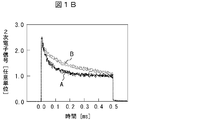
- FIG. 1B shows the result of acquiring the transient response of the secondary electron signal under pulsed electron irradiation.
- the secondary electron signal shows a pulse shape of 0.5 ms, which is the same as the pulse width of irradiation.
- the secondary electron signal attenuates during pulsed electron irradiation and becomes steady.
- the sample surface is positively charged. This positive charging attenuates the secondary electron emission from the sample, and as a result, it becomes steady in a state where the number of irradiated electrons and the number of secondary electrons emitted are equal.
- the irradiation time is 0.01 ms or less immediately after the start of irradiation, and the secondary electron signal is steady. If the irradiation time is 0.4 ms or more, the secondary electron signal between the region A and the region B There is almost no difference.
- the difference in the secondary electron signal between the region A and the region B increases. That is, an image reflecting the buried structure appears in a specific time region where a difference occurs in the secondary electron signal.
- the present invention has been made on the basis of the research on the transient response of the secondary electron signal, and the observation method using the pulsed electron beam according to the present invention has the detection timing and the detection time in the secondary electron detection. It includes a process of controlling. According to this method, a time region for detecting a secondary electron signal during pulsed electron irradiation can be selected. As shown in FIG. 1B, the sample information appears in a specific time region during irradiation. By selecting the secondary electron detection time region, secondary electron signals that do not have the necessary sample information and secondary electron signals that contain unnecessary information can be removed, so that an improvement in image quality can be expected.
- the step of irradiating a plurality of pulsed electrons to the same location and the timing of detecting secondary electrons are performed at least one or more of the plurality of pulsed electrons. It includes the process of synchronizing with. Sample information appears at a specific number of pulsed electron irradiations. According to this method, since a secondary electron signal from pulsed electrons having necessary information can be selectively acquired, an improvement in information selectivity can be expected in addition to image quality.
- the observation method using the pulsed electron beam of the present invention has at least one of a step of irradiating a plurality of pulsed electrons to the same location under different intermittent conditions and a timing of detecting secondary electrons.
- the method includes the step of synchronizing with the above pulsed electrons. Sample information appears in the process of relaxation of the state induced by irradiation. According to this method, since the electron irradiation process for inducing the state and the electron irradiation used for imaging can be separated, an improvement in image quality can be expected.
- the first intermittent condition is an intermittent condition in which the sample is charged by electron irradiation
- the second intermittent condition is an intermittent condition in which charging of the sample is detected.
- the intermittent condition is the second intermittent condition.
- the first intermittent condition is a condition for irradiating 100 to 10000 electrons
- the second intermittent condition is an intermittent condition for irradiating 1 to 100 electrons.
- the interval between the intermittent condition and the second intermittent condition is 0.001 ms to 1000 ms.
- the second intermittent condition is a condition in which the same location is irradiated a plurality of times, and includes a step of integrating and imaging secondary electron detection signals obtained in synchronization with the second intermittent condition.
- image quality improvement by signal integration can be expected.
- the observation method using the pulsed electron beam of the present invention has at least two or more irradiations when the same location is irradiated with a plurality of pulses under different intermittent conditions having different numbers of irradiation times, pulse widths, and interval times between pulses. It includes a step of selecting an intermittent condition and synchronizing the timing for detecting secondary electrons with the selected intermittent condition, and a step of imaging the synchronously detected secondary electrons for each selected intermittent condition. According to this method, it is possible to visualize a plurality of pieces of sample information in a single sequence, so that improvement in sample analysis efficiency can be expected.
- the first intermittent condition is a condition reflecting the surface form
- the second intermittent condition is a condition for processing the charging of the sample
- the third intermittent condition is a condition for controlling the charging, and is detected.
- the selected intermittent conditions to synchronize are the first and third intermittent conditions.
- the first and second intermittent conditions are executed when the pulsed electrons are irradiated to the same location under the first intermittent condition and the second intermittent condition. And a step of changing the detection timing of the secondary electrons in synchronization with the change of the interval.
- the relaxation process of the state induced by the first intermittent condition can be observed by time resolution.
- the incident energy of the intermittent electron beam is 1 eV to 3000 eV.
- the observation method using the pulsed electron beam according to the present invention includes a step of setting the intermittent condition of the pulsed electron and the detection condition of the secondary electron based on the transient characteristics of the secondary electron. According to this method, suitable observation conditions can be set in a short time.
- a scanning electron microscope using an electron beam comprises: means for emitting an electron beam; means for intermittently irradiating an electron beam; means for controlling the intermittent condition of the electron beam; Means for positioning the irradiation position; means for focusing the electron beam on the sample; means for detecting secondary electrons from the sample; means for controlling the detection timing and detection time of the secondary electrons; It has means for forming an image from a detection signal of secondary electrons and the irradiation position, and means for displaying the image.
- the scanning electron microscope using the electron beam of the present invention comprises means for emitting an electron beam, means for intermittently irradiating the electron beam, means for controlling the intermittent condition of the electron beam, and the electron Means for positioning the irradiation position of the beam, means for focusing the electron beam on the sample, means for detecting secondary electrons from the sample, means for selecting a pulse for detecting the secondary electrons, and 2 It has means for forming an image from a detection signal of secondary electrons and the irradiation position, and means for displaying the image.
- the signal having the necessary sample information can be selectively detected by controlling the detection time region of the secondary electron signal, it is possible to observe and analyze the sample form with high image quality and high information selectivity. .
- FIG. 2 is a cross-sectional view of a sample used in Example 1.
- FIG. Explanatory drawing which shows the time change of a secondary electron signal.
- the block diagram which shows an example of the electron microscope of this invention.
- FIG. 3 is an explanatory diagram regarding image formation by SEM.
- FIG. 3 is an explanatory diagram illustrating an example of an imaging method according to the first embodiment.
- FIG. 3 is a diagram illustrating an example of a secondary electron signal profile used in the imaging method according to the first embodiment.
- FIG. 3 is a diagram illustrating an example of an image acquired by the imaging method according to the first embodiment.
- Sectional drawing which shows an example of the sample of Example 2.
- FIG. The figure which shows an example of the irradiation time chart of a pulsed electron.
- Explanatory drawing which shows the signal change of the secondary electron under several pulsed electron irradiation.
- Explanatory drawing which shows an example of the time chart of pulsed electron irradiation and detection of Example 2.
- FIG. The block diagram which shows an example of the electron microscope of this invention.
- Explanatory drawing which shows an example of the time chart of pulsed electron irradiation and detection of Example 3.
- FIG. Explanatory drawing which shows the relationship between the pulsed electron irradiation of Example 3, and secondary electron emission.
- Explanatory drawing which shows an example of the time chart of pulsed electron irradiation and detection of Example 4.
- FIG. which shows an example of the time chart of pulsed electron irradiation and detection of Example 5.
- FIG. 10 is a configuration diagram illustrating an example of an electron microscope according to an eighth embodiment. Explanatory drawing which shows an example of the time chart of irradiation and detection of the pulsed electron and energy beam of Example 8.
- FIG. 10 is a configuration diagram showing an example of an electron microscope of Example 9.
- FIG. The figure which shows the electron emission signal under pulsed electron irradiation at the time of applying a positive voltage to an electric field control electrode.
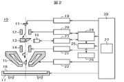
- the scanning electron microscope 10 includes an electron optical system, a stage mechanism system, a control system, an image processing system, and an operation system.
- the electron optical system includes an electron gun 11, a pulse generator 12, a diaphragm 13, a deflector 14, an objective lens 15, and a detector 16.
- the stage mechanism system includes a sample holder 17 and a sample 18 on an XYZ stage.
- the control system includes an electron gun control unit 19, a pulse control unit 20, a deflection scanning signal control unit 21, an objective lens coil control unit 22, and a detector control unit 23.
- the image processing system includes a detection signal processing unit 24, an image forming unit 25, and an image display unit 26.
- the operation system includes an operation interface 27 and an SEM control unit 28.
- the pulse generator 12 is separately provided.
- the present invention can also be implemented using an electron gun capable of irradiating an electron beam with a pulse.
- the pulse control unit can be incorporated in the electron gun control unit.
- FIGS. 3A and 3B An imaging method under pulsed electron beam irradiation in the present embodiment is shown in FIGS. 3A and 3B.
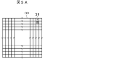
- FIG. 3A explains SEM image formation.
- the secondary electron signal from the irradiation position controlled by the deflector 14 is detected and the brightness of the pixel 31 is obtained. Secondary electron signals are detected while changing the irradiation position.
- An image is formed from the coordinates of the irradiation position and the intensity of the secondary electron signal. In this embodiment, the same portion is defined by the same pixel.
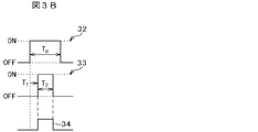
- FIG. 3B shows a relationship between a time chart 32 of intermittent conditions of pulsed electrons irradiated to the same pixel, a time chart 33 of detector control, and a signal waveform 34 of secondary electrons obtained at this time.
- the intermittent condition in this embodiment is a pulse width.
- Pulsed electron as shown in the time chart 32, by the pulse control unit 20, is intermittently irradiated to a single pixel at a pulse width T p.
- Secondary electrons in pulsed electron irradiation as shown in the time chart 33 of the detector control, at timing T 1 and the detection time T 2, is detected, the secondary electron signal waveform 34 is obtained.
- the pulse width T p is 0.5 ms
- the timing T 1 is 0.1 ms
- the detection time T 2 is 0.2 ms.
- the detector control unit 23 controls the detection timing and the detection time.
- all the secondary electron signals included in the irradiation time are acquired, and the detection signal processing unit 24 performs data processing.
- the secondary electron signal included in the time domain may be cut out.
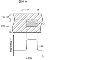
- FIG. 4B shows the result of observing the sample of FIG. 1A with an electron beam incident energy of 300 eV using the imaging method under pulsed electron beam irradiation.
- the depth that can be visualized at 300 eV is about 10 nm.
- the incident energy of the electron beam of 300 eV is used.
- the energy in the range of 1 eV to 3000 eV can be set in consideration of the restriction of the apparatus according to the present invention and the imaging target.
- the region where the polysilicon 3 is buried as shown in the secondary electron signal profile 40 in FIG. 4A and the SEM image 41 in FIG. 4B by controlling the pulsed electron irradiation and the detection timing and detection time of the secondary electrons. Gives a bright contrast. Since the observed polysilicon 3 has a cylindrical shape (for example, a plug in a semiconductor element) in this embodiment, the upper surface is circular as shown in FIG. 4B and the cross section is rectangular as shown in FIG. 4A. Yes.
- a time region including necessary sample information can be selected and a secondary electron signal can be detected, so that sample analysis with high image quality is possible.
- FIG. 6B An imaging method in the case where a plurality of pulsed electrons are irradiated to the same location will be described.
- the apparatus has the same configuration as that shown in FIG.
- a sample used in this example is shown in FIG.
- the sample has a laminated structure of an oxide film 51 and a polysilicon film 52.
- the interface between the oxide film and the polysilicon film is divided into a region A having a normal interface and a region B having a rough interface 53.
- the relationship between the secondary electron signal and the number of pulses was examined. The result is shown in FIG. 6B.
- FIG. 6A is a pulse electron irradiation time chart.
- the intermittent condition of the electron beam was set such that the pulse width T p was 0.05 ms, the interval T 1 between pulses was 0.5 ms, and the number N of irradiated pulses was 12 shots.
- FIG. 6B is a diagram showing the relationship between the secondary electron signal and the number of irradiation pulses in region A and region B. In the drawing, the intensity of the secondary electron signal obtained corresponding to the 12th pulse from the 1st irradiation pulse is shown in an arbitrary scale.
- the secondary electron signal was an average value of secondary electron signals included in the pulse. Both region A and region B are attenuated as the number of pulses increases, and become steady.
- N the number of pulses
- the imaging method under pulsed electron beam irradiation in this embodiment is shown in FIG.
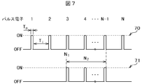
- the time chart 70 represents the electron beam intermittent condition. Intermittent conditions in the present embodiment are the pulse width, the interval between pulses, and the number of pulsed electron irradiations.
- the pulsed electrons are controlled by a pulse width T p , an interval T i between pulses, and an intermittent condition of N pulses. Pulsed electrons having the intermittent condition are irradiated to the same location. In the present embodiment, the same portion is defined by the same pixel, and here, it is sufficient that a plurality of pulses are irradiated in the same pixel.
- the detector controller 23 In synchronism with the pulse electron shown in the time chart 70, as shown in the time chart 71, the detector controller 23, a detection start pulse N 1, the detection pulse number N 2 is controlled.
- the pulse width T p is 0.05 ms
- the interval between pulses T 1 0.5 ms
- the number of irradiated pulses N 12 shots
- the detection start pulse N 1 3
- the number of detection pulses N 2 6. It was.
- all the secondary electrons during the designated pulse irradiation are acquired.
- the detection timing and the detection time in the pulse are designated. It doesn't matter.
- the detector control unit 23 selects the detection pulse. However, all secondary electron signals included in a plurality of pulses irradiated to the same location are acquired, and the detection signal processing unit 24 is obtained. The secondary electron signal included in the detection pulse may be cut out by the data processing according to. As described above, by using the present embodiment, a pulse including necessary sample information can be selected and a secondary electron signal can be detected, so that sample analysis with high image quality becomes possible.
- FIG. 80 A configuration example of the scanning electron microscope in this embodiment is shown in FIG.
- the scanning electron microscope 80 differs from the scanning electron microscope 10 shown in FIG.
- the beam splitter 81 once splits the electron beam into two, and the multi-pulse generator 82 capable of setting the interrupt condition for each electron beam, the pulse electrons 83 having the first interrupt condition, Pulsed electrons 84 having two intermittent conditions are generated.
- the pulsed electrons having the first and second intermittent conditions are focused on the same location by the objective lens. In this embodiment, the same place is defined by the overlap of the irradiation areas.
- the pulsed electron irradiation regions having the first and second intermittent conditions overlap, and the pulsed electrons having the first and second intermittent conditions need to be the same irradiation region. Absent.
- the electron beam is divided to control a plurality of intermittent conditions.
- the pulse control unit 20 generates a control signal that combines a plurality of intermittent conditions.
- the pulsed electrons having the first and second intermittent conditions can be controlled.
- the imaging method under pulsed electron beam irradiation in this embodiment is shown in FIG.
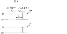
- the time chart 90 is a single chart and represents the first and second intermittent conditions.
- the intermittent condition in this embodiment is a pulse width and an interval between pulses.
- the pulse electrons are controlled by a pulse width T p1 which is a first intermittent condition and a pulse width T p2 which is a second intermittent condition, and the first pulse electrons and the second pulse electrons are synchronized at an interval T i . And irradiated.
- the secondary electron signal is detected in synchronization with the second pulse.
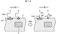
- a pulsed electron imaging method will be described by taking as an example the case of observing the buried structure shown in FIG. Similar to FIG. 1A, the sample is composed of a region A of the silicon oxide film 2 and a region B in which the polysilicon 3 is embedded in the silicon oxide film.
- the sample charge 101 generated by the first pulsed electrons 100 is accumulated according to the buried form of the sample, so that a difference occurs between the region A and the region B. Further, the sample charge 101, in regions A and B, since the different time constants of charge relaxation, the difference is enlarged at intervals T i.
- the sample pulse When the sample pulse is irradiated with the second pulsed electrons 102, a difference occurs in the signal pulse 103 of the secondary electrons in accordance with the charge holding amount.
- the first pulsed electron 100 In order to obtain the difference in the sample charging 101, it is desirable that the first pulsed electron 100 is in a condition where several thousand electrons are irradiated.
- the number of electrons is obtained by multiplying the amount of current (I) obtained from the irradiated electron beam by the pulse width (t) of the applied pulse and dividing the result by the amount of elementary charge (q). Can do.
- the second pulsed electron 102 is in a condition that several tens of electrons are irradiated so as not to break the sample charging 101 formed by the first pulsed electron.
- the interval T i is preferably set within the range of 0.001 ms to 1000 ms, which is about the time constant of dielectric relaxation.
- the first pulsed electrons 100 are pulsed irradiation for forming the sample charge 101 and do not contribute to the image.
- the detector control unit 23 is configured to detect synchronously with the second pulse condition, but acquires all secondary electron signals included in a plurality of pulse electronic conditions irradiated to the same location,
- the secondary electron signal included in the second pulse condition may be cut out by data processing by the detection signal processing unit 24.
- an image can be formed by separating the pulse for processing the sample charge and the pulse for detecting the sample charge, so that the selectivity of information is improved and sample analysis with high image quality is possible. Become.
- the apparatus has the same configuration as that shown in FIG.
- the time chart 110 is one chart and represents the first and second intermittent conditions. Intermittent conditions in the present embodiment are the pulse width, the interval between pulses, and the number of pulsed electron irradiations.
- the pulse electrons are controlled by a pulse width T p1 which is a first intermittent condition and a pulse width T p2 which is a second intermittent condition, and the first pulse electrons and the second pulse electrons are synchronized at an interval T i1 . And irradiated.
- the second pulse electrons are irradiated N times at an interval T i2 .
- the second pulsed electrons are irradiated N times so that the charging does not proceed, and the interval T i2 is adjusted. At this time, it is desirable that the total number of second pulse electrons irradiated N times is equal to the number of charges relaxed in the interval T i2 or the difference is 100 or less.
- the secondary electron signal is detected in synchronization with the second pulse.
- the detected N ⁇ 1 secondary electron signals are integrated by the detection signal processing unit 24 to be a signal for one pixel.
- the detector control unit 23 is configured to detect synchronously with the second pulse condition, but acquires all secondary electron signals included in a plurality of pulse electronic conditions irradiated to the same location,
- the secondary electron signal included in the second pulse condition may be extracted and integrated by data processing by the detection signal processing unit 24. In this way, if this embodiment is used, the pulses constituting the image can be integrated, so that sample analysis with high image quality becomes possible.
- an imaging method of a pulsed electron beam that irradiates the same location under a plurality of intermittent conditions and visualizes images with different sample information at once will be described.
- the apparatus has the same configuration as that shown in FIG. A plurality of pulse electronic conditions were controlled by the pulse controller 20.
- a plurality of memories are installed in the image forming unit 25, and the signal from the detection signal processing unit 24 can be selected and written. With this apparatus, a plurality of images can be processed at once.
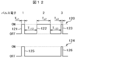
- the imaging method under pulsed electron beam irradiation in this embodiment is shown in FIG.
- the time chart 120 is a single chart and represents the first, second, and third intermittent conditions. Intermittent conditions in the present embodiment are the pulse width, the interval between pulses, and the number of pulsed electron irradiations.
- Pulsed electron includes a pulse width T p1 of the first pulsed electron 121, and the pulse width T p2 of the second pulsed electron 122 is controlled by the pulse width T p3 of the third pulsed electron 123, the first pulse electronic and said second pulse electrons, an interval T i12, wherein the second pulsed electron third pulse electrons are irradiated in synchronization with interval T i23.
- the secondary electron signal is detected in synchronization with the first pulse, and the second secondary electron detected in synchronization with the third pulse of the first secondary electron signal 125 to be detected.
- Each signal 126 is stored in a separate memory. Eventually, two types of images are formed by the first secondary electron signal 125 and the second secondary electron signal 126.
- a pulse electron imaging method will be described by taking as an example a case where the surface shape and the buried structure shown in FIG. 13 are observed simultaneously.
- a sample used in this example is shown in FIG.
- the sample is composed of a region A of the silicon oxide film 2 and a region B in which the polysilicon 3 is embedded in the silicon oxide film. Further, the region B has a stepped shape on the surface.
- the first pulsed electrons are set to irradiation conditions in which charging under electron beam irradiation hardly affects the secondary electron signal. At this time, the secondary electron signal depends on the surface morphology.
- the amount of secondary electron emission differs depending on the change in the angle of the sample and the edge, a difference occurs in the first secondary electron signal 125 between the region A and the region B.
- the charge 130 is formed by the second pulse electrons, and the charge is detected by the third pulse electrons.
- the second secondary electron signal 126 obtained at this time reflects the buried structure of the sample.
- an image can be formed by classifying pulse electrons having a plurality of intermittent conditions into different pieces of sample information, so that a plurality of pieces of sample information can be visualized and analyzed simultaneously.
- an imaging method of a pulsed electron beam that irradiates the same location under a plurality of intermittent conditions and visualizes temporal changes in sample information will be described.
- the apparatus has the same configuration as that shown in FIG. A plurality of pulse electronic conditions were controlled by the pulse controller 20.
- a plurality of memories are installed in the image forming unit 25, and the signal from the detection signal processing unit 24 can be selected and written. With this device, multiple images can be processed at once.
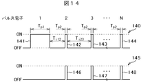
- the imaging method under pulsed electron beam irradiation in this embodiment is shown in FIG.
- the time chart 140 represents the first and second intermittent conditions with one chart. Intermittent conditions in the present embodiment are the pulse width, the interval between pulses, and the number of pulsed electron irradiations.
- the first pulse electrons 141 are irradiated with the pulse width T p1
- the second pulse electrons 142 and the subsequent pulses are irradiated N times with the pulse width T p2 .
- the interval between the pulse electrons can be set as interval T i12 , interval T i23 .
- a pulse electron imaging method will be described by taking as an example the case of observing the buried structure shown in FIG. 1A.
- Charge is formed on the surface by the first pulsed electrons.
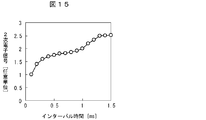
- the second pulse is irradiated while changing the interval time T i12 from the first pulsed electron, as shown in FIG. 15, according to the interval T i12 between the first pulsed electron and the second pulsed electron.
- a signal change of secondary electrons can be obtained. Since the amount of charge relaxation obtained by the first pulse electrons varies depending on the length of the interval, the secondary electron signal obtained by the second pulse electrons changes.
- the amount of charge relaxation is due to the buried structure of the sample and has a plurality of time constants as shown in FIG.
- the internal structure can be analyzed by analyzing the time constant. By acquiring the dependence of the interval time on each pixel, the internal three-dimensional structure can be restored.
- the second to Nth pulse electrons for charge detection acquired at different intervals are stored in each memory, and a time-resolved image of charge is acquired.
- a three-dimensional structure can be constructed by the time-resolved image analysis. As described above, when this embodiment is used, a time-resolved image of charging can be acquired, so that a three-dimensional structure can be analyzed.
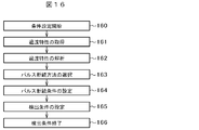
- FIG. 16 is a flowchart showing the imaging condition setting method in this embodiment.
- the intermittent condition and detection condition of the pulsed electron beam are determined from the transient characteristics of the secondary electron signal.
- the transient characteristic of the secondary electron signal includes a method of estimating from a database in which the transient characteristic is acquired in advance, and a method of acquiring the transient characteristic at a random position on the sample.
- a method for acquiring transient characteristics at random positions on a sample will be described as an example.
- a random position on the sample is automatically or manually selected, and the change of the secondary electron signal during the pulse irradiation of FIG. 1B and the inter-pulse interval time dependency of the secondary electron signal of FIG. 14 are acquired (step 161). . From FIG. 1B and FIG.
- step 162 it is possible to analyze the irradiation electron quantity at the time of stationary signal of the secondary electrons and the signal relaxation time constant (step 162).
- the steady-state irradiation electron quantity obtained from the random position is compared with the relaxation time constant, and the intermittent condition of the pulse irradiation is determined (step 163).
- the difference in the amount of irradiation electrons in the steady state is larger than the difference in the relaxation time constant, it is desirable to set the single pulse of the first embodiment, and when the difference in the relaxation time constant is larger, the embodiment It is desirable to irradiate a plurality of pulsed electrons shown in 2 or 3.
- the case of irradiating a plurality of pulsed electrons in Example 2 will be described as an example.
- a suitable pulse width is set from the difference in the amount of regularly irradiated electrons, and a suitable interval between pulses and the number of irradiations are set from the difference in relaxation time constant (step 164).
- the detection condition is selected in consideration of the time domain where necessary information is obtained and the SN of the image (step 165). Also, for example, as shown in FIG. 6 of the second embodiment, it is possible to set the detection condition by acquiring the relationship between the number of pulses and the secondary electron signal. Thereafter, the condition setting is finished and the observation can be started (step 166).
- FIG. 17 shows a GUI for setting the imaging conditions in the present embodiment.
- the GUI shown in FIG. 17 is displayed on the monitor of the operation interface 27.
- a window 170 is a window for acquiring a transient characteristic of the secondary electron signal, and displays transient characteristic data such as a change in the secondary electron signal during pulse irradiation and an inter-pulse interval time dependency of the secondary electron signal.
- the window 171 displays a characteristic value analyzed from the result of the transient characteristic of the secondary electron signal.
- a pulse intermittent method can be selected in the window 172 from the transient characteristic data and the characteristic value. Further, the intermittent condition can be set by the window 173, and the detection condition can be set by the window 174. As described above, by using the present embodiment, it is possible to easily set the imaging conditions, so that an image can be acquired in a short time.
- an imaging method of a pulsed electron beam for visualizing a sample form with an intermittent energy beam and an intermittent electron beam at the same location will be described.
- the configuration of the apparatus is shown in FIG.
- An intermittent energy beam source 181 and an energy beam control unit 182 are added to the apparatus configuration of FIG.
- a pulse laser is used as an intermittent energy source.
- the present invention can use energy rays such as X-rays, light, and infrared rays, and is not limited to this embodiment.
- FIG. 19 shows an imaging method under pulsed electron beam irradiation in this example.
- the time chart 190 is one chart and represents the first intermittent condition and the second intermittent condition. Intermittent conditions in the present embodiment are the pulse width, the interval between pulses, and the number of pulsed electron irradiations. In the present embodiment, the first pulse electrons and the second pulse electrons, which are different intermittent conditions, are irradiated to the same location.
- a time chart 191 shows the irradiation timing of the pulse laser. The pulse laser is irradiated between the first pulsed electron and the second pulsed electron.
- the time chart 192 shows the detection timing of the secondary electrons. In this embodiment, the time chart 192 is synchronized with the second pulsed electrons.
- the charge relaxation characteristics of the sample processed with the first pulse change depending on the response of the dielectric polarization by the pulse laser. Since the change in the relaxation characteristics depends on the composition and structure of the sample, the secondary electron signal by the second pulsed electrons reflects the composition and structure of the sample.
- this embodiment it is possible to select not only the sample information depending on the state induced by the electron beam irradiation but also the information, and the types of sample information that can be analyzed can be expanded.
- an analysis method using a pulsed electron beam that identifies an intermittent electron beam and detects secondary electrons while controlling the trajectory of the secondary electrons emitted from the sample will be described.
- FIG. 21 is a diagram showing the relationship between the direction of the electric field and the secondary electron trajectory. As shown in FIG. 21A, when a positive voltage is applied to the electrode 201 with respect to the sample, secondary electrons are accelerated by the electric field between the sample and the electrode, and secondary electrons of all energy are emitted from the sample. . If there are more secondary electrons emitted than primary electrons, the surface of the sample is positively charged.
- FIG. 21B when a negative voltage is applied to the electrode 201 with respect to the sample, the secondary electrons are attenuated by the electric field between the sample and the electrode, and the secondary electrons with some energy are Returned to Depending on the amount of secondary electrons returned to the sample, the sample is negatively charged.
- FIG. 22 is a cross-sectional view of a sample having a buried interface used in this example.
- a buried interface 221 exists in the silicon carbide 222.
- the buried interface 221 is a stacking fault included in the silicon carbide crystal.
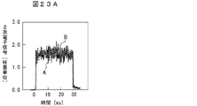
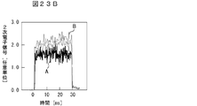
- FIG. 22 shows an electron emission signal under pulsed electron irradiation when a positive voltage is applied to the electrode 201 (FIG. 23A) and 2 under pulsed electron irradiation when a negative voltage is applied to the electrode 201. It is a secondary electron emission signal (FIG. 23B).
- a positive voltage there is no difference in the signal during pulse irradiation between the region A where there is no buried interface and the region B where there is a buried interface, and even if the detection timing is adjusted, there is no difference between the regions A and B.
- the secondary electron emission signal difference cannot be obtained.
- the secondary emission electron signal changes transiently in the region B where the buried interface exists.
- the stacking fault which is the interface where the region B is buried has a property of easily capturing electrons.
- region A secondary electrons returned by the electric field flow out through the sample.
- region B the returned secondary electrons are captured and negatively charged.
- the secondary emission electron signal changes transiently.
- the difference in the secondary electron emission signal between the regions A and B immediately after the pulse electron irradiation is small, and the difference in the secondary electron emission signal is maximum at 10 to 30 ms. Therefore, when the pulsed electron irradiation and detection time chart of FIG.
- the transient characteristics due to charging can be controlled according to the sample, so that the selectivity of information is improved and the sample analysis with high image quality is possible.
Landscapes
- Chemical & Material Sciences (AREA)
- Analytical Chemistry (AREA)
- Physics & Mathematics (AREA)
- Electromagnetism (AREA)
- General Physics & Mathematics (AREA)
- Analysing Materials By The Use Of Radiation (AREA)
Abstract
Description
ここで、断続的な電子線の入射エネルギは1eVから3000eVである。
本実施例における走査電子顕微鏡の構成例を図2に示す。走査電子顕微鏡10は電子光学系、ステージ機構系、制御系、画像処理系、操作系により構成されている。電子光学系は電子銃11、パルス生成器12、絞り13、偏向器14、対物レンズ15、検出器16により構成されている。ステージ機構系はXYZステージ上の試料ホルダ17、試料18、により構成されている。制御系は電子銃制御部19、パルス制御部20、偏向走査信号制御部21、対物レンズコイル制御部22、検出器制御部23により構成されている。画像処理系は、検出信号処理部24、画像形成部25、画像表示部26により構成されている。操作系は、操作インターフェース27とSEM制御部28により構成されている。本願発明では、別途パルス生成器12を設ける構成としたが、パルスで電子線照射可能な電子銃を用いても実施可能である。この場合、パルス制御部は、電子銃制御部に組み込むことも可能である。
2:シリコン酸化膜、
3:ポリシリコン、
10:走査電子顕微鏡、
11:電子銃、
12:パルス発生器、
13:絞り、
14:偏向器、
15:対物レンズ、
16:検出器、
17:試料ホルダ、
18:試料、
19:電子銃制御部、
20:パルス制御部、
21:偏向制御部、
22:対物レンズコイル制御部、
23:検出器制御部、
24:検出信号処理部、
25:画像形成部、
26:画像表示部、
27:操作インターフェース、
28:SEM制御部、
30:画像、
31:画素、
32,33:タイムチャート、
34:信号波形、
40:プロファイル、
41:SEM画像、
50:試料、
51:酸化膜、
52:ポリシリコン、
53:界面、
70,71:タイムチャート、
80:走査電子顕微鏡、
81:ビーム分割器、
82:マルチパルス生成器、
83,84:パルス電子、
90,91:タイムチャート、
100:パルス電子、
101:試料帯電、
102:パルス電子、
103:信号パルス、
110,111:タイムチャート、
120:タイムチャート、
121,122,123:パルス電子、
124:タイムチャート、
125,126:2次電子信号、
130:試料帯電、
140:タイムチャート、
141,142,143,144:パルス電子、
145:タイムチャート、
146,147,148:パルス電子、
170,171,172,173,174:ウィンドウ、
181:エネルギ線源、
182:エネルギ線源制御部、
190,191,192:タイムチャート。
Claims (19)
- 電子線を試料に照射して前記試料から放出された電子を検出し、前記試料が有する形態を画像化する電子線を用いた撮像方法において、
前記試料の観察予定領域に前記電子線を所定時間照射する電子線照射工程と、
前記電子線照射工程の所定照射時間内にあって該所定照射時間より短い時間に設定された検出時間で、前記試料から放出された電子を検出する放出電子検出工程と、
前記放出された電子の検出信号に基づいて前記試料の形態を画像化する画像化工程とを含む
ことを特徴とする電子線を用いた撮像方法。 - 前記電子線照射工程において、前記所定時間の照射を複数回繰り返し、
前記複数回繰り返し照射のうちの少なくとも1回の電子線照射中に、前記試料から放出された電子を検出する
ことを特徴とする請求項1記載の電子線を用いた撮像方法。 - 前記電子線照射工程において、前記所定時間が第1の照射時間と該第1の照射時間と異なる第2の照射時間からなり、少なくとも第1および第2の照射時間を用いて前記試料の観察予定領域に前記第1の照射時間と前記第2の照射時間との間にインターバル時間を設けて電子線を照射し、
前記2つの照射時間の少なくとも1つの照射時間を持つ電子線照射中に、前記試料から放出された電子を検出する
ことを特徴とする請求項1記載の電子線を用いた撮像方法。 - 前記第1の照射時間の間に前記試料に帯電がなされ、
前記第2の照射時間の間に、前記試料の帯電を検出する
ことを特徴とする請求項3記載の電子線を用いた撮像方法。 - 前記第2の照射時間で照射される回数が複数回であって、
前記第2の照射時間に同期して、前記試料から放出された電子を検出する工程と、
前記第2の照射時間に同期して検出された複数回の放出された電子を積算し、画像化する工程を含む
ことを特徴とする請求項4記載の電子線を用いた撮像方法。 - 前記第1の照射時間に照射される電子数が100個から10000個の範囲であって、
前記第2の照射時間に照射される電子数が1個から100個の範囲であって、
前記第1の照射時間から前記第2の照射時間が実行されるまでのインターバル時間が、0.001msから1000msである
ことを特徴とする請求項4記載の電子線を用いた撮像方法。 - 前記第1の照射時間に照射される電子数が100個から10000個の範囲であって、
前記第2の照射時間に照射される電子数が1個から100個の範囲であって、
前記第1の照射時間から前記第2の照射時間が実行されるまでのインターバル時間が、0.001msから1000msである
ことを特徴とする請求項5記載の電子線を用いた撮像方法。 - 前記電子線の入射エネルギが、1eVから3000eVである
ことを特徴とする請求項7記載の電子線を用いた撮像方法。 - 前記放出された電子の過渡特性を取得し、該過渡特性に基づいて前記電子線の照射時間と前記試料から放出された電子の検出条件とを設定する
ことを特徴とする請求項8記載の電子線を用いた撮像方法。 - 前記電子線照射工程において、前記試料の観察予定領域に前記電子線を照射する照射時間を複数種備え、
前記放出電子検出工程は、前記複数種の照射時間のうち、少なくとも二種の照射時間を選択し、前記選択した二種の照射時間のそれぞれに同期して前記試料から放出された電子を検出し、
前記画像化工程は、前記放出された電子の検出信号に基づいて、少なくとも二つの種類の試料形態を画像化する
ことを特徴とする請求項1記載の電子線を用いた撮像方法。 - 前記複数種の照射時間は、前記試料の表面形態を反映すべく照射時間が設定された第1の照射時間と、
前記試料の帯電を制御すべく照射時間が設定された第2の照射時間と、
前記試料の帯電を検出すべく照射時間が設定された第3の照射時間とから構成され、
前記選択した照射時間が、前記第1の照射時間と前記第2の照射時間である
ことを特徴とする請求項10記載の電子線を用いた撮像方法。 - 前記電子線照射工程において、前記試料の観察予定領域に第1の照射時間と該第1の照射時間と異なる第2の照射時間とを備え、
前記第1照射時間終了から前記第2の照射時間が実行されるまでのインターバル時間を変化させる工程を有し、
前記放出電子検出工程は、前記インターバル時間の変化毎に照射される第2の照射時間に同期して、前記試料から放出された電子を検出し、
前記画像化工程において、前記放出された電子の検出信号により、前記インターバル時間の変化毎の画像を形成する
ことを特徴とする請求項1記載の電子線を用いた撮像方法。 - 前記放出された電子の過渡特性を取得し、該過渡特性に基づいて前記電子線の照射時間と前記試料から放出された電子の検出条件とを設定する
ことを特徴とする請求項12記載の電子線を用いた撮像方法。 - 前記電子線の照射と異なるタイミングで断続的にエネルギ線を照射する工程を、さらに有し、
前記放出電子検出工程において、前記電子線を所定時間照射する条件に同期して、前記試料から放出された電子を検出する
ことを特徴とする請求項1記載の電子線を用いた撮像方法。 - 前記試料に電子線が照射される界面付近の電界を制御する工程を、さらに有し、
前記電子線照射工程における前記電子線の照射条件に基づいて、前記放出された電子を検出し、前記検出信号を用いて前記試料の特性を解析する
ことを特徴とする請求項1記載の電子線を用いた撮像方法。 - 電子線を放出する電子銃と、
前記電子線を断続的に照射するパルス電子形成部と、
前記パルス電子を断続的に照射する断続条件を設定するパルス電子制御部と、
前記パルス電子の照射位置を制御する偏向器と、
前記パルス電子を試料に集束照射する電子光学系と、
前記試料を保持する試料ホルダと、
前記試料から放出された電子を検出する検出器と、
前記検出器の検出タイミングと検出時間を制御する検出制御部と、
前記検出制御により検出された電子の信号と前記照射位置データから、画像を形成する画像形成部と、
前記画像形成部により得られる画像を表示する画像表示部と、を有し、
前記パルス電子制御部は、前記試料の観察予定領域に前記電子線を照射する所定時間と照射回数と該照射間のインターバル時間を設定し、
前記検出制御部は、前記設定された所定照射時間内にあって該所定照射時間より短い検出時間を設定する
ことを特徴とする電子顕微鏡。 - 前記検出制御部は、前記検出器の複数の検出タイミングと検出時間を制御し、
前記複数のタイミングで検出された電子の信号を複数の記憶部に保存する信号記憶部を有し、
前記画像形成部において、前記信号と前記照射位置から、複数の画像を形成する
ことを特徴とする請求項16記載の電子顕微鏡。 - 前記パルス電子の照射位置に断続的なエネルギ線を照射する照射系を、さらに有し、
前記パルス電子制御部は、前記断続条件に基づいて、前記エネルギ線の照射条件を制御する
ことを特徴とする請求項16記載の電子顕微鏡。 - 前記電子線が照射される前記試料の界面に対向して設置され、前記試料からの電界を制御する電極部をさらに、有し、
前記電極部に印加する極性に応じて、前記試料から放出された電子の進路を制御する
ことを特徴とする請求項16記載の電子顕微鏡。
Priority Applications (2)
| Application Number | Priority Date | Filing Date | Title |
|---|---|---|---|
| KR1020137031719A KR101478940B1 (ko) | 2011-06-03 | 2012-05-24 | 전자 현미경 및 전자선을 사용한 촬상 방법 |
| US14/123,744 US8907279B2 (en) | 2011-06-03 | 2012-05-24 | Electron microscope and image capturing method using electron beam |
Applications Claiming Priority (2)
| Application Number | Priority Date | Filing Date | Title |
|---|---|---|---|
| JP2011125475A JP5744629B2 (ja) | 2011-06-03 | 2011-06-03 | 電子顕微鏡及び電子線を用いた撮像方法 |
| JP2011-125475 | 2011-06-03 |
Publications (1)
| Publication Number | Publication Date |
|---|---|
| WO2012165293A1 true WO2012165293A1 (ja) | 2012-12-06 |
Family
ID=47259150
Family Applications (1)
| Application Number | Title | Priority Date | Filing Date |
|---|---|---|---|
| PCT/JP2012/063320 Ceased WO2012165293A1 (ja) | 2011-06-03 | 2012-05-24 | 電子顕微鏡及び電子線を用いた撮像方法 |
Country Status (4)
| Country | Link |
|---|---|
| US (1) | US8907279B2 (ja) |
| JP (1) | JP5744629B2 (ja) |
| KR (1) | KR101478940B1 (ja) |
| WO (1) | WO2012165293A1 (ja) |
Cited By (2)
| Publication number | Priority date | Publication date | Assignee | Title |
|---|---|---|---|---|
| WO2019207668A1 (ja) * | 2018-04-25 | 2019-10-31 | 株式会社 日立ハイテクノロジーズ | 荷電粒子線装置の照射条件決定方法、及び荷電粒線装置 |
| WO2022091180A1 (ja) * | 2020-10-26 | 2022-05-05 | 株式会社日立ハイテク | 荷電粒子線装置 |
Families Citing this family (24)
| Publication number | Priority date | Publication date | Assignee | Title |
|---|---|---|---|---|
| JP6121651B2 (ja) * | 2012-04-04 | 2017-04-26 | 株式会社日立ハイテクノロジーズ | 電子顕微鏡、電子顕微鏡の観察条件の設定方法、および電子顕微鏡による観察方法 |
| US9846133B2 (en) * | 2012-11-19 | 2017-12-19 | Hitachi, Ltd. | Semiconductor inspection device including a counter electrode with adjustable potentials used to obtain images for detection of defects, and inspection method using charged particle beam |
| JP6169451B2 (ja) * | 2013-09-13 | 2017-07-26 | 株式会社日立ハイテクノロジーズ | 荷電粒子線装置および荷電粒子線の計測方法 |
| JP6289339B2 (ja) * | 2014-10-28 | 2018-03-07 | 株式会社日立ハイテクノロジーズ | 荷電粒子線装置及び情報処理装置 |
| JP6379018B2 (ja) | 2014-11-20 | 2018-08-22 | 株式会社日立ハイテクノロジーズ | 荷電粒子線装置および検査方法 |
| EP3133633B1 (en) * | 2016-02-24 | 2018-03-28 | FEI Company | Studying dynamic specimen behavior in a charged-particle microscope |
| US10879037B2 (en) | 2016-04-27 | 2020-12-29 | Hitachi High-Tech Corporation | Charged particle beam device with distance setting between irradiation regions in a scan line |
| JP6736498B2 (ja) * | 2017-02-23 | 2020-08-05 | 株式会社日立ハイテク | 計測装置及び観測条件の設定方法 |
| DE112017007270B4 (de) * | 2017-04-21 | 2023-03-30 | Hitachi High-Tech Corporation | Ladungsträgerstrahlvorrichtung und Verfahren zum Einstellen von Bedingungen in einer Ladungsträgerstrahlvorrichtung |
| WO2019123604A1 (ja) * | 2017-12-21 | 2019-06-27 | 株式会社日立ハイテクノロジーズ | 荷電粒子線装置 |
| DE102018120630B3 (de) * | 2018-08-23 | 2019-10-31 | Carl Zeiss Microscopy Gmbh | Verfahren zum Bearbeiten eines Objekts und Programm zur Steuerung eines Partikelstrahlsystems |
| WO2020136044A2 (en) * | 2018-12-28 | 2020-07-02 | Asml Netherlands B.V. | Pulsed charged-particle beam system |
| JP7108788B2 (ja) * | 2019-05-21 | 2022-07-28 | 株式会社日立ハイテク | 荷電粒子線装置 |
| JP7271358B2 (ja) | 2019-07-25 | 2023-05-11 | 株式会社日立ハイテク | 電気特性を導出するシステム及び非一時的コンピューター可読媒体 |
| US11127562B1 (en) * | 2020-08-05 | 2021-09-21 | Fei Company | System and method for RF pulsed electron beam based STEM |
| WO2022059202A1 (ja) * | 2020-09-18 | 2022-03-24 | 株式会社日立ハイテク | 検査システム |
| AU2022259406A1 (en) | 2021-04-16 | 2023-11-02 | Integrated Dynamic Electron Solutions, Inc. | Arbitrary electron dose waveforms for electron microscopy |
| JP7054281B1 (ja) * | 2021-10-19 | 2022-04-13 | 株式会社Photo electron Soul | 電子線適用装置および電子線適用装置における検出データの作成方法 |
| EP4246551A1 (en) * | 2022-03-14 | 2023-09-20 | Jeol Ltd. | Charged particle beam apparatus and control method for charged particle beam apparatus |
| DE102023200591A1 (de) * | 2023-01-25 | 2024-07-25 | Carl Zeiss Smt Gmbh | Verfahren und vorrichtung zum kontaktlosen einstellen einer elektrostatischen aufladung einer probe |
| US11848173B1 (en) * | 2023-01-31 | 2023-12-19 | Integrated Dynamic Electron Solutions, Inc. | Methods and systems for event modulated electron microscopy |
| US12237147B2 (en) * | 2023-01-31 | 2025-02-25 | Integrated Dynamic Electron Solutions, Inc. | Methods and systems for event modulated electron microscopy |
| JPWO2024257200A1 (ja) * | 2023-06-13 | 2024-12-19 | ||
| WO2026013751A1 (ja) * | 2024-07-09 | 2026-01-15 | 株式会社日立ハイテク | 荷電粒子線装置および試料の検査方法 |
Citations (4)
| Publication number | Priority date | Publication date | Assignee | Title |
|---|---|---|---|---|
| JPH02295043A (ja) * | 1989-05-10 | 1990-12-05 | Hitachi Ltd | 電子ビームによる電圧測定装置 |
| JP2002043378A (ja) * | 2000-07-24 | 2002-02-08 | Advantest Corp | 電子ビームテスタ、試験方法 |
| JP2006140162A (ja) * | 2005-11-21 | 2006-06-01 | Hitachi Ltd | 試料像形成方法 |
| JP2006286685A (ja) * | 2005-03-31 | 2006-10-19 | Renesas Technology Corp | 半導体集積回路装置の製造方法 |
Family Cites Families (3)
| Publication number | Priority date | Publication date | Assignee | Title |
|---|---|---|---|---|
| JPS58197643A (ja) | 1982-05-12 | 1983-11-17 | Toshiba Corp | ストロボ走査電子顕微鏡装置 |
| JP3823073B2 (ja) | 2002-06-21 | 2006-09-20 | 株式会社日立ハイテクノロジーズ | 電子線を用いた検査方法及び検査装置 |
| JP4443167B2 (ja) | 2003-08-25 | 2010-03-31 | 株式会社日立製作所 | 走査型電子顕微鏡 |
-
2011
- 2011-06-03 JP JP2011125475A patent/JP5744629B2/ja active Active
-
2012
- 2012-05-24 KR KR1020137031719A patent/KR101478940B1/ko active Active
- 2012-05-24 US US14/123,744 patent/US8907279B2/en active Active
- 2012-05-24 WO PCT/JP2012/063320 patent/WO2012165293A1/ja not_active Ceased
Patent Citations (4)
| Publication number | Priority date | Publication date | Assignee | Title |
|---|---|---|---|---|
| JPH02295043A (ja) * | 1989-05-10 | 1990-12-05 | Hitachi Ltd | 電子ビームによる電圧測定装置 |
| JP2002043378A (ja) * | 2000-07-24 | 2002-02-08 | Advantest Corp | 電子ビームテスタ、試験方法 |
| JP2006286685A (ja) * | 2005-03-31 | 2006-10-19 | Renesas Technology Corp | 半導体集積回路装置の製造方法 |
| JP2006140162A (ja) * | 2005-11-21 | 2006-06-01 | Hitachi Ltd | 試料像形成方法 |
Cited By (6)
| Publication number | Priority date | Publication date | Assignee | Title |
|---|---|---|---|---|
| WO2019207668A1 (ja) * | 2018-04-25 | 2019-10-31 | 株式会社 日立ハイテクノロジーズ | 荷電粒子線装置の照射条件決定方法、及び荷電粒線装置 |
| JPWO2019207668A1 (ja) * | 2018-04-25 | 2021-05-13 | 株式会社日立ハイテク | 荷電粒子線装置の照射条件決定方法、及び荷電粒子線装置 |
| US11232929B2 (en) | 2018-04-25 | 2022-01-25 | Hitachi High-Tech Corporation | Method for determining irradiation conditions for charged particle beam device and charged particle beam device |
| WO2022091180A1 (ja) * | 2020-10-26 | 2022-05-05 | 株式会社日立ハイテク | 荷電粒子線装置 |
| JPWO2022091180A1 (ja) * | 2020-10-26 | 2022-05-05 | ||
| JP7377375B2 (ja) | 2020-10-26 | 2023-11-09 | 株式会社日立ハイテク | 荷電粒子線装置 |
Also Published As
| Publication number | Publication date |
|---|---|
| US8907279B2 (en) | 2014-12-09 |
| US20140097342A1 (en) | 2014-04-10 |
| JP5744629B2 (ja) | 2015-07-08 |
| KR20140018365A (ko) | 2014-02-12 |
| KR101478940B1 (ko) | 2014-12-31 |
| JP2012252913A (ja) | 2012-12-20 |
Similar Documents
| Publication | Publication Date | Title |
|---|---|---|
| JP5744629B2 (ja) | 電子顕微鏡及び電子線を用いた撮像方法 | |
| EP3172758B1 (en) | Method for inspecting a sample using an assembly comprising a scanning electron microscope and a light microscope | |
| JP6957641B2 (ja) | 荷電粒子線装置およびそれを用いた試料観察方法 | |
| JP6121651B2 (ja) | 電子顕微鏡、電子顕微鏡の観察条件の設定方法、および電子顕微鏡による観察方法 | |
| JP6025910B2 (ja) | 電子線を用いた撮像方法および電子線装置 | |
| KR102794066B1 (ko) | 하전 입자선 장치 | |
| US10879037B2 (en) | Charged particle beam device with distance setting between irradiation regions in a scan line | |
| US20190228948A1 (en) | Scanning Electron Microscope and Measurement Method | |
| US20120091339A1 (en) | Charged-particle microscope device, and method of controlling charged-particle beams | |
| JP2007207688A (ja) | ミラー電子顕微鏡およびミラー電子顕微鏡を用いた検査装置 | |
| JP5222994B2 (ja) | 試料観察方法および走査電子顕微鏡 | |
| US11011348B2 (en) | Scanning electron microscope and sample observation method using scanning electron microscope | |
| KR102478945B1 (ko) | 하전 입자선 장치의 조사 조건 결정 방법, 및 하전 입자선 장치 | |
| JP2013201076A (ja) | 試料分析装置および試料分析方法 | |
| JP5833207B2 (ja) | 試料分析装置および試料分析方法 |
Legal Events
| Date | Code | Title | Description |
|---|---|---|---|
| 121 | Ep: the epo has been informed by wipo that ep was designated in this application |
Ref document number: 12793194 Country of ref document: EP Kind code of ref document: A1 |
|
| ENP | Entry into the national phase |
Ref document number: 20137031719 Country of ref document: KR Kind code of ref document: A |
|
| NENP | Non-entry into the national phase |
Ref country code: DE |
|
| WWE | Wipo information: entry into national phase |
Ref document number: 14123744 Country of ref document: US |
|
| 122 | Ep: pct application non-entry in european phase |
Ref document number: 12793194 Country of ref document: EP Kind code of ref document: A1 |