WO2012165284A1 - 表示装置の駆動回路および駆動方法 - Google Patents
表示装置の駆動回路および駆動方法 Download PDFInfo
- Publication number
- WO2012165284A1 WO2012165284A1 PCT/JP2012/063295 JP2012063295W WO2012165284A1 WO 2012165284 A1 WO2012165284 A1 WO 2012165284A1 JP 2012063295 W JP2012063295 W JP 2012063295W WO 2012165284 A1 WO2012165284 A1 WO 2012165284A1
- Authority
- WO
- WIPO (PCT)
- Prior art keywords
- signal line
- data signal
- circuit
- charge
- discharge
- Prior art date
- Legal status (The legal status is an assumption and is not a legal conclusion. Google has not performed a legal analysis and makes no representation as to the accuracy of the status listed.)
- Ceased
Links
Images






Classifications
-
- G—PHYSICS
- G09—EDUCATION; CRYPTOGRAPHY; DISPLAY; ADVERTISING; SEALS
- G09G—ARRANGEMENTS OR CIRCUITS FOR CONTROL OF INDICATING DEVICES USING STATIC MEANS TO PRESENT VARIABLE INFORMATION
- G09G3/00—Control arrangements or circuits, of interest only in connection with visual indicators other than cathode-ray tubes
- G09G3/20—Control arrangements or circuits, of interest only in connection with visual indicators other than cathode-ray tubes for presentation of an assembly of a number of characters, e.g. a page, by composing the assembly by combination of individual elements arranged in a matrix no fixed position being assigned to or needed to be assigned to the individual characters or partial characters
- G09G3/34—Control arrangements or circuits, of interest only in connection with visual indicators other than cathode-ray tubes for presentation of an assembly of a number of characters, e.g. a page, by composing the assembly by combination of individual elements arranged in a matrix no fixed position being assigned to or needed to be assigned to the individual characters or partial characters by control of light from an independent source
- G09G3/36—Control arrangements or circuits, of interest only in connection with visual indicators other than cathode-ray tubes for presentation of an assembly of a number of characters, e.g. a page, by composing the assembly by combination of individual elements arranged in a matrix no fixed position being assigned to or needed to be assigned to the individual characters or partial characters by control of light from an independent source using liquid crystals
- G09G3/3611—Control of matrices with row and column drivers
- G09G3/3685—Details of drivers for data electrodes
-
- G—PHYSICS
- G09—EDUCATION; CRYPTOGRAPHY; DISPLAY; ADVERTISING; SEALS
- G09G—ARRANGEMENTS OR CIRCUITS FOR CONTROL OF INDICATING DEVICES USING STATIC MEANS TO PRESENT VARIABLE INFORMATION
- G09G3/00—Control arrangements or circuits, of interest only in connection with visual indicators other than cathode-ray tubes
- G09G3/20—Control arrangements or circuits, of interest only in connection with visual indicators other than cathode-ray tubes for presentation of an assembly of a number of characters, e.g. a page, by composing the assembly by combination of individual elements arranged in a matrix no fixed position being assigned to or needed to be assigned to the individual characters or partial characters
- G09G3/34—Control arrangements or circuits, of interest only in connection with visual indicators other than cathode-ray tubes for presentation of an assembly of a number of characters, e.g. a page, by composing the assembly by combination of individual elements arranged in a matrix no fixed position being assigned to or needed to be assigned to the individual characters or partial characters by control of light from an independent source
- G09G3/36—Control arrangements or circuits, of interest only in connection with visual indicators other than cathode-ray tubes for presentation of an assembly of a number of characters, e.g. a page, by composing the assembly by combination of individual elements arranged in a matrix no fixed position being assigned to or needed to be assigned to the individual characters or partial characters by control of light from an independent source using liquid crystals
- G09G3/3611—Control of matrices with row and column drivers
- G09G3/3648—Control of matrices with row and column drivers using an active matrix
-
- G—PHYSICS
- G09—EDUCATION; CRYPTOGRAPHY; DISPLAY; ADVERTISING; SEALS
- G09G—ARRANGEMENTS OR CIRCUITS FOR CONTROL OF INDICATING DEVICES USING STATIC MEANS TO PRESENT VARIABLE INFORMATION
- G09G3/00—Control arrangements or circuits, of interest only in connection with visual indicators other than cathode-ray tubes
- G09G3/20—Control arrangements or circuits, of interest only in connection with visual indicators other than cathode-ray tubes for presentation of an assembly of a number of characters, e.g. a page, by composing the assembly by combination of individual elements arranged in a matrix no fixed position being assigned to or needed to be assigned to the individual characters or partial characters
- G09G3/34—Control arrangements or circuits, of interest only in connection with visual indicators other than cathode-ray tubes for presentation of an assembly of a number of characters, e.g. a page, by composing the assembly by combination of individual elements arranged in a matrix no fixed position being assigned to or needed to be assigned to the individual characters or partial characters by control of light from an independent source
- G09G3/36—Control arrangements or circuits, of interest only in connection with visual indicators other than cathode-ray tubes for presentation of an assembly of a number of characters, e.g. a page, by composing the assembly by combination of individual elements arranged in a matrix no fixed position being assigned to or needed to be assigned to the individual characters or partial characters by control of light from an independent source using liquid crystals
- G09G3/3611—Control of matrices with row and column drivers
- G09G3/3696—Generation of voltages supplied to electrode drivers
-
- G—PHYSICS
- G09—EDUCATION; CRYPTOGRAPHY; DISPLAY; ADVERTISING; SEALS
- G09G—ARRANGEMENTS OR CIRCUITS FOR CONTROL OF INDICATING DEVICES USING STATIC MEANS TO PRESENT VARIABLE INFORMATION
- G09G3/00—Control arrangements or circuits, of interest only in connection with visual indicators other than cathode-ray tubes
- G09G3/20—Control arrangements or circuits, of interest only in connection with visual indicators other than cathode-ray tubes for presentation of an assembly of a number of characters, e.g. a page, by composing the assembly by combination of individual elements arranged in a matrix no fixed position being assigned to or needed to be assigned to the individual characters or partial characters
- G09G3/2007—Display of intermediate tones
- G09G3/2014—Display of intermediate tones by modulation of the duration of a single pulse during which the logic level remains constant
Definitions
- the present invention relates to a display device such as a liquid crystal display device, and more particularly to a drive circuit and a drive method for driving a data signal line of the display device.
- Liquid crystal display devices are characterized by thinness and low power consumption, and are used for various purposes. Liquid crystal display devices are also used in portable devices that operate on batteries, for example.
- display screens of portable devices have been increasing in screen size and resolution. As the screen size increases and the resolution increases, the load on the driving circuit of the liquid crystal panel increases and the operating frequency of the driving circuit increases. For this reason, the power consumption of the liquid crystal display device increases. Therefore, in order to reduce the battery size of portable devices, liquid crystal display devices are required to further reduce power consumption.
- the power consumption of the liquid crystal display device is roughly classified into power consumption of the liquid crystal panel (power consumption due to charging / discharging) and power consumption of the drive circuit.
- a method for reducing the power consumption of the drive circuit is examined.
- the power consumption of the drive circuit can be reduced by devising the circuit configuration.
- the power consumption of the drive circuit can be reduced by reducing the number of analog circuits through which a steady current flows.
- a conventional general liquid crystal display device drives a data signal line (also called a video signal line, a source bus line, etc.) using a drive circuit including an analog buffer circuit. Since a steady current flows through the analog buffer circuit, the analog buffer circuit causes an increase in power consumption of the liquid crystal display device. Therefore, as a method of driving the data signal line without using the analog buffer circuit, only two kinds of voltages (charge voltage and discharge voltage) are switched and applied to the data signal line, and the time for applying the two kinds of voltages is applied.
- a method of changing the length of the video signal according to the video signal (hereinafter referred to as pulse width modulation driving) has been conventionally known.
- Patent Document 1 discloses a method of writing a voltage less than a voltage applied to a data signal line to a pixel, or displaying gradation by shifting a waveform of a scanning signal line and a data signal line, and data A method for inverting every other pixel polarity in the signal line direction is described.
- Patent Document 2 describes a method of equalizing the difference between the voltage of the scanning signal line and the voltage of the data signal line during positive-polarity writing and negative-polarity writing when performing pulse width modulation driving.
- Patent Document 3 describes a method of applying a voltage having a vibration component that vibrates during one horizontal period to the data signal line as a method of driving the data signal line other than the pulse width modulation drive.
- the analog buffer circuit included in the data signal line driving circuit can be deleted, and the power consumption of the display device can be reduced.
- the pulse width modulation drive has a problem in that the data signal line cannot be driven accurately when the time constant during charging of the data signal line varies. This problem becomes significant in a display device having a large number of data signal lines and a large number of gradations.
- Patent Documents 1 and 2 do not describe how to solve this problem.
- the method described in Patent Document 3 since the voltage of the data signal line is vibrated, charging / discharging of the load capacity is frequently performed, and useless power is consumed. Further, the method described in Patent Document 3 has a problem that it cannot be applied to a display device having a large number of gradations.
- an object of the present invention is to provide a driving circuit that accurately drives a data signal line by using pulse width modulation driving, and a display device that accurately displays gradation using the driving circuit.
- a first aspect of the present invention is a drive circuit for driving a data signal line of a display device, A pattern generation circuit for generating a plurality of patterns each having a pulse width corresponding to a gradation for each gradation; A selection circuit that selects one pattern from the patterns generated by the pattern generation circuit based on gradation data given to each data signal line and a set of patterns designated for each data signal line When, A charge / discharge control circuit for obtaining a charge control signal and a discharge control signal based on the pattern selected by the selection circuit; A charge / discharge circuit for switching and applying a charge voltage and a discharge voltage to the data signal line according to the charge control signal and the discharge control signal;
- the charge / discharge circuit includes a charge transistor that applies the charge voltage to the data signal line according to the charge control signal, and a discharge transistor that applies the discharge voltage to the data signal line according to the discharge control signal. It is characterized by.
- a correction pulse generation circuit that generates a plurality of types of correction pulses having a predetermined width;
- the charge / discharge control circuit selects one correction pulse designated for each data signal line from the correction pulses generated by the correction pulse generation circuit, and the charge control signal is selected based on the selected correction pulse. Is changed to a level instructing charging.
- the charge / discharge circuit includes a plurality of the charge transistors, and at the time of charge, use one or more transistors designated according to the temperature for each data signal line among the plurality of charge transistors. It is characterized by.
- the charge / discharge control circuit controls both the charge transistor and the discharge transistor in an off state during a voltage holding period set within one horizontal period.
- the charge / discharge control circuit is the charge control signal in the first period, the first control signal that is the discharge control signal in the second period, the discharge control signal in the first period, and the charge control signal in the second period.
- the charging / discharging circuit includes a first transistor that functions as the charging transistor or the discharging transistor according to the first control signal, and a second transistor that functions as the discharging transistor or the charging transistor according to the second control signal. It is characterized by including.
- a seventh aspect of the present invention is the sixth aspect of the present invention.
- the charge / discharge circuit includes a plurality of the first and second transistors, and is designated according to the temperature for each of the data signal lines from among the plurality of first transistors during charging within a first period. One or more transistors are used, and at the time of charging within the second period, one or more transistors designated according to the temperature for each data signal line are used from among the plurality of second transistors.
- the charging time of the data signal line within one horizontal period is less than or equal to twice the time constant when the data signal line is charged.
- the charging time of the data signal line within one horizontal period is 2.3 times or less of the time constant when the data signal line is charged.
- One horizontal period is 4.5 times or more of a time constant when the data signal line is charged.
- An eleventh aspect of the present invention is a display device that performs gradation display, A display panel including a plurality of scanning signal lines, a plurality of data signal lines, and a plurality of pixel circuits; A scanning signal line driving circuit for sequentially selecting the scanning signal lines; A data signal line driving circuit for applying a gradation voltage corresponding to a video signal to the data signal line,
- the data signal line driving circuit includes: A pattern generation circuit for generating a plurality of patterns each having a pulse width corresponding to a gradation for each gradation; A selection circuit that selects one pattern from the patterns generated by the pattern generation circuit based on gradation data given to each data signal line and a set of patterns designated for each data signal line When, A charge / discharge control circuit for obtaining a charge control signal and a discharge control signal based on the pattern selected by the selection circuit; And a charge / discharge circuit for switching and applying a charge voltage and a discharge voltage to the data signal line in accordance with the charge control signal and the discharge control signal
- a twelfth aspect of the present invention is a driving method for driving a data signal line of a display device, Generating a plurality of sets of patterns each having a pulse width corresponding to a gradation; Selecting one pattern from the generated patterns based on gradation data given for each data signal line and a set of patterns designated for each data signal line; Obtaining a charge control signal and a discharge control signal based on the selected pattern; Switching and applying a charge voltage and a discharge voltage to the data signal line according to the charge control signal and the discharge control signal.
- a thirteenth aspect of the present invention is a method for driving a display device having a display panel having a plurality of scanning signal lines, a plurality of data signal lines, and a plurality of pixel circuits, and performing gradation display. Sequentially selecting the scanning signal lines; Generating a plurality of sets of patterns each having a pulse width corresponding to a gradation; Selecting one pattern from the generated patterns based on gradation data given for each data signal line and a set of patterns designated for each data signal line; Obtaining a charge control signal and a discharge control signal based on the selected pattern; Switching and applying a charge voltage and a discharge voltage to the data signal line according to the charge control signal and the discharge control signal.
- a plurality of patterns corresponding to each gradation are generated, and which pattern is used is selected for each data signal line.
- the second aspect of the present invention it is possible to configure a charge / discharge circuit that switches and applies a charge voltage and a discharge voltage to the data signal line using the charge transistor and the discharge transistor.
- a plurality of types of correction pulses are generated, and which correction pulse is used is selected for each data signal line.
- a plurality of charging transistors are provided, and which charging transistor is used is selected for each data signal line according to the temperature.
- the data signal line can be accurately driven using a suitable charging transistor for each data signal line.
- the voltage holding period within one horizontal period, the voltage of the data signal line can be reliably written to the pixel circuit connected to the data signal line.
- the sixth aspect of the present invention it is possible to configure a charge / discharge circuit that uses the first and second transistors to switch and apply the charge voltage and the discharge voltage to the data signal line.
- a plurality of first and second transistors are provided, and which one is used as a charging transistor is selected for each data signal line according to the temperature.
- the data signal line can be accurately driven using a suitable charging transistor for each data signal line.
- the charging time within one horizontal period of the data signal line to be twice or 2.3 times the time constant at the time of charging the data signal line, It is possible to effectively use time by reducing useless charging time.
- the voltage of the data signal line is set to a plurality of levels within one horizontal period by setting one horizontal period to 4.5 times or more the time constant at the time of charging the data signal line. Sufficient time can be ensured to reach.
- the eleventh or thirteenth aspect of the present invention it is possible to accurately display gradation using a driving circuit or a driving method capable of accurately driving a data signal line.
- FIG. 1 is a block diagram illustrating a configuration of a liquid crystal display device according to a first embodiment of the present invention.
- FIG. 2 is a diagram illustrating a configuration of a data signal line driving circuit of the liquid crystal display device illustrated in FIG. 1.
- FIG. 3 is a signal waveform diagram of the data signal line driving circuit shown in FIG. 2. It is a figure which shows the load model of a data signal line.
- FIG. 3 is a diagram showing data stored in a PWM pattern generation circuit of the data signal line drive circuit shown in FIG. 2.
- FIG. 3 is a diagram showing data stored in a PWM pattern designating circuit of the data signal line driving circuit shown in FIG. 2.
- FIG. 8 is a signal waveform diagram of the data signal line driving circuit shown in FIG. 7. It is a figure which shows the data memorize
- FIG. 13 is a diagram showing data stored in a transistor designating circuit of the data signal line driving circuit shown in FIG. 12. It is a figure which shows the structure of the data signal line drive circuit of the liquid crystal display device which concerns on the 4th Embodiment of this invention.
- FIG. 15 is a signal waveform diagram of the data signal line driving circuit shown in FIG. 14. It is a figure which shows the charging / discharging circuit of the data signal line drive circuit which concerns on the modification of embodiment of this invention.
- FIG. 1 is a block diagram showing the configuration of the liquid crystal display device according to the first embodiment of the present invention.
- a liquid crystal display device 1 shown in FIG. 1 includes a liquid crystal panel 2, a display control circuit 3, a scanning signal line driving circuit 4, and a data signal line driving circuit 10.
- the liquid crystal display device 1 performs gradation display of 2 p level (p is an integer of 2 or more) based on the video signal X output from the display control circuit 3.
- p is an integer of 2 or more
- m is an integer of 1 or more
- n is an even number of 2 or more
- i is an odd number of 1 to n
- j is an integer of 1 to n.
- the liquid crystal panel 2 includes m scanning signal lines G1 to Gm, n data signal lines S1 to Sn, and (m ⁇ n) pixel circuits 5.
- the scanning signal lines G1 to Gm are arranged in parallel to each other.
- the data signal lines S1 to Sn are arranged in parallel to each other so as to be orthogonal to the scanning signal lines G1 to Gm.
- the scanning signal lines G1 to Gm and the data signal lines S1 to Sn intersect at (m ⁇ n) locations.
- a total of (m ⁇ n) pixel circuits 5 are arranged corresponding to (m ⁇ n) intersections.
- the pixel circuit 5 is connected to one scanning signal line and one data signal line.
- the display control circuit 3 outputs a timing control signal TC1 to the scanning signal line driving circuit 4, and outputs a timing control signal TC2 and a video signal X to the data signal line driving circuit 10.
- the timing control signal TC1 includes, for example, a gate start pulse and a gate clock.
- the timing control signal TC2 includes, for example, a source start pulse and a source clock.
- the scanning signal line driving circuit 4 sequentially selects the scanning signal lines G1 to Gm based on the timing control signal TC1. Thereby, the n pixel circuits 5 connected to the selected scanning signal line are selected at once.
- the data signal line drive circuit 10 applies gradation voltages corresponding to the video signal X to the data signal lines S1 to Sn based on the timing control signal TC2. As a result, n gradation voltages are written into the n pixel circuits 5 selected by the scanning signal line driving circuit 4.
- the luminance of the pixel circuit 5 is determined by the gradation voltage written in the pixel circuit 5.
- An image can be displayed on the liquid crystal panel 2 by writing gradation voltages in all the pixel circuits 5 using the scanning signal line driving circuit 4 and the data signal line driving circuit 10.
- the liquid crystal display device 1 performs dot inversion driving for inverting the polarity of the gradation voltage written in the pixel circuit 5 for each adjacent pixel circuit 5.
- writing a positive voltage (negative voltage) to the pixel circuit 5 connected to the odd-numbered (even-numbered) data signal line is referred to as first writing, and is connected to the odd-numbered (even-numbered) data signal line.
- Writing a negative voltage (positive voltage) to the pixel circuit 5 is referred to as second writing.
- the data signal line driving circuit 10 alternately performs the first writing and the second writing every horizontal period.
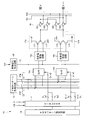
- FIG. 2 is a diagram showing a configuration of the data signal line driving circuit 10.
- the data signal line drive circuit 10 includes a data register 11, a PWM pattern generation circuit 12, a control signal generation circuit 13, a PWM pattern designation circuit 14, n selectors 15, and n charge / discharge control circuits. 16, n charge / discharge circuits 17 and (n / 2) polarity selection circuits 18 are included.
- n charge / discharge circuits 17 and (n / 2) polarity selection circuits 18 are included.
- two selectors 15a and 15b, two charge / discharge control circuits 16a and 16b, two charge / discharge circuits 17a and 17b, and one A polarity selection circuit 18 is provided.
- FIG. 2 only the circuit for driving the two data signal lines Si and Si + 1 is shown, but the circuits for driving the other data signal lines have the same structure.
- the video signal X output from the display control circuit 3 in one horizontal period includes n pieces of p-bit gradation data.
- the gradation data corresponding to the jth data signal line Sj is referred to as Xj.
- the display control circuit 3 may output gradation data one by one in order or may output a plurality of gradation data in order.
- the data register 11 stores n pieces of gradation data X1 to Xn output from the display control circuit 3, and outputs them in parallel during one horizontal period. More specifically, the data register 11 includes two (n ⁇ p) -bit registers (not shown). The n pieces of gradation data output from the display control circuit 3 are sequentially written in the first register. At the time of the first writing, the n pieces of gradation data are written in the first register as they are. At the time of the second writing, the n pieces of gradation data are written in the first register by switching the odd number and the even number. After the writing to the first register is completed, the n pieces of gradation data are collectively transferred from the first register to the second register.
- the data register 11 outputs the output signal of the second register.
- the data register 11 outputs n grayscale data in the order of X1, X2, X3, X4,..., Xn ⁇ 1, Xn at the time of the first writing, and n grayscale data at the time of the second writing. Output in the order of X1, X4, X3,..., Xn, Xn-1.
- FIG. 2 shows a state at the time of the first writing.
- the selectors 15a and 15b, the charge / discharge control circuits 16a and 16b, the charge / discharge circuits 17a and 17b, and the polarity selection circuit 18 are respectively supplied to the grayscale data output from the data register 11 with respect to the data signal lines Si and Si + 1. A gradation voltage corresponding to Xi and Xi + 1 is applied.
- the PWM pattern generation circuit 12, the control signal generation circuit 13, and the PWM pattern designation circuit 14 output signals necessary for the operation of the selector 15 and the charge / discharge control circuit 16.
- the data signal line driving circuit 10 applies only two kinds of voltages (charging voltage and discharging voltage) to the data signal line, and changes the length of time for applying the two kinds of voltages in accordance with the video signal. Width modulation drive is performed.
- the pulse width modulation driving performed by the data signal line driving circuit 10 generates a plurality of sets of PWM (Pulse Width Modulation) patterns corresponding to the polarity of the gradation and the gradation voltage (positive polarity or negative polarity). Whether to use the PWM pattern is selected for each data signal line (details will be described later).
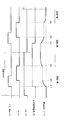
- FIG. 3 is a signal waveform diagram of the data signal line driving circuit 10. The operation of the data signal line driving circuit 10 will be described with reference to FIGS.
- the PWM pattern generation circuit 12 generates a plurality of PWM patterns corresponding to combinations of gradations and polarity of gradation voltages.
- the PWM pattern includes a positive PWM pattern PTP corresponding to a positive voltage and a negative PWM pattern PTM corresponding to a negative voltage.
- FIG. 3A shows three types of positive PWM patterns corresponding to the gradations L1, L2, and L3.
- the PWM pattern generated by the data signal line driving circuit 10 changes to a high level at a predetermined time within one horizontal period (for example, at time t11 in the case of the gradation L1), and at time t3 within one horizontal period. Change to low level.
- the length of the high level period of the PWM pattern is determined according to the gradation and the polarity of the gradation voltage.
- the control signal generation circuit 13 outputs a control signal ZC based on the timing control signal TC2 output from the display control circuit 3. As shown in FIG. 3B, the control signal ZC changes to high level at time t2 within one horizontal period, and changes to low level at time t4 within one horizontal period. However, time t2 is after the latest time when the PWM pattern changes to the high level and before time t3. Time t4 is later than time t3. A period in which the control signal ZC is at a low level and the PWM pattern is at a high level is a charging period in which a charging voltage is applied to the data signal line.
- a period in which both the control signal ZC and the PWM pattern are at a low level is a discharge period in which a discharge voltage is applied to the data signal line.
- the period in which the control signal ZC is at a high level is a voltage holding period in which the data signal line is in a high impedance state. By providing the voltage holding period, the voltage of the data signal line Sj can be reliably written to the pixel circuit 5.
- the data register 11 outputs the gradation data Xi to the selector 15a and outputs the gradation data Xi + 1 to the selector 15b.
- a plurality of positive PWM patterns PTP generated by the PWM pattern generation circuit 12 are input to the selector 15a.
- the selector 15a selects one positive PWM pattern from the plurality of positive PWM patterns PTP based on the gradation data Xi.
- a plurality of negative side PWM patterns PTM generated by the PWM pattern generation circuit 12 are input to the selector 15b.
- the selector 15b selects one negative PWM pattern from a plurality of negative PWM patterns PTM based on the gradation data Xi + 1.
- the charge / discharge control circuit 16a receives the control signal ZC and the positive PWM pattern selected by the selector 15a.
- the charge / discharge circuit 17 a is a CMOS switch including two transistors 171 and 172.
- the output voltage of the charge / discharge circuit 17a becomes the positive charge voltage VP during the charge period and becomes the discharge voltage (ground voltage) during the discharge period.
- the output of the charge / discharge circuit 17a is in a high impedance state.
- the output voltage of the charge / discharge circuit 17 a is output to the outside of the data signal line drive circuit 10 via the polarity selection circuit 18.
- the output voltage of the data signal line driving circuit 10 changes as shown in FIG. FIG. 3C shows a change in the output voltage of the data signal line driving circuit 10 corresponding to the above three gradations.
- the output voltage of the data signal line driving circuit 10 changes to VP at time t11 and changes to zero at time t4.
- the output of the data signal line driving circuit 10 is in a high impedance state from time t2 to t4.
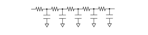
- the data signal line Si becomes a load of the data signal line driving circuit 10.
- This load is modeled as a CR distributed constant circuit as shown in FIG.
- the voltage of the data signal line Si changes due to the integration action of the CR distributed constant circuit.
- the voltage of the data signal line Si changes as shown in FIG. FIG. 3D shows changes in the voltage of the data signal line Si corresponding to the above three gradations.
- the voltage of the data signal line Si starts increasing at time t11, stops increasing at time t2, and becomes substantially constant from time t2 to t4.
- the voltage of the data signal line Si starts to decrease at time t4 and eventually returns to zero.
- the charge / discharge control circuit 16b receives the control signal ZC and the negative PWM pattern selected by the selector 15b.
- the charge / discharge circuit 17b is a CMOS switch including two transistors 173 and 174.
- the output voltage of the charge / discharge circuit 17b becomes the negative charge voltage VM in the charge period and becomes the discharge voltage in the discharge period.
- the output of the charge / discharge circuit 17b is in a high impedance state.
- the output voltage of the data signal line driving circuit 10 and the voltage of the data signal line Si + 1 change in the opposite directions to those in FIGS.
- the voltage of the data signal line Sj is written in the pixel circuit selected by the scanning signal line driving circuit 4 among the pixel circuits 5 in the j-th column.
- the length of the high-level period of the PWM pattern is determined according to the gradation and the polarity of the gradation voltage. For this reason, the charging time of the data signal line differs depending on the gradation, and the voltage after charging (voltage at time t2, hereinafter referred to as the reached voltage) also differs.
- the reached voltage voltage after charging
- the data signal line Si is charged only for time T1, and the ultimate voltage is V1.
- the data signal line is charged only for a time T2 (T2 ⁇ T1), and the ultimate voltage is V2 (V2 ⁇ V1). Therefore, by suitably determining the length of the high-level period of the PWM pattern according to the gradation and the polarity of the gradation voltage, the gradation display is applied by applying the gradation voltage corresponding to the video signal to the data signal line. It can be carried out.
- the data signal line driving circuit 10 uses a plurality of sets of PWM patterns corresponding to combinations of gradations and polarity of gradation voltages.
- the PWM pattern generation circuit 12 generates a plurality of sets of PWM patterns for each gradation, with one horizontal period as a cycle and a pulse width corresponding to the gradation. More specifically, the PWM pattern generation circuit 12 generates 2 q sets (q is an integer of 1 or more) of PWM patterns.
- the set of PWM pattern, corresponding to 2 p number of gradations, include the 2 p pieces of positive PWM pattern and 2 p pieces of negative PWM pattern.
- PWM pattern generating circuit 12 outputs the 2 p + q pieces of positive PWM pattern PTP, a 2 p + q + 1 single PWM pattern consisting of 2 p + q pieces of negative PWM pattern PTM.
- the PWM pattern generated by the PWM pattern generation circuit 12 changes to high level at different times within one horizontal period, and changes to low level at the same time within one horizontal period. Such a PWM pattern can be defined using only the change timing to the high level.
- the PWM pattern generation circuit 12 stores the change timing to the high level (hereinafter referred to as “on timing”) for all the PWM patterns.
- the on-timing represents, for example, the time from the beginning of one horizontal period until the PWM pattern changes to a high level with a predetermined accuracy.
- the PWM pattern generation circuit 12 may store the ON timing in a fixed manner or may store it in a rewritable manner.
- the total data amount of on-timing stored in the PWM pattern generation circuit 12 is (2 p + q + 1 ⁇ d) bits.
- the PWM pattern generation circuit 12 has a function of changing the corresponding PWM pattern to high level when the time indicated by the on-timing has elapsed from the beginning of one horizontal period, and a function of changing all PWM patterns to low level at time t3. And have. As long as it has these functions, the configuration of the PWM pattern generation circuit 12 may be arbitrary.
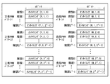
- the PWM pattern designating circuit 14 designates which of the 2 q sets of PWM patterns is used for each data signal line. More specifically, as shown in FIG. 6, the PWM pattern designating circuit 14 sets the number of PWM patterns to be used among the 2 q sets of PWM patterns for each data signal line Sj (hereinafter referred to as pattern set number Yj). Is remembered.
- One pattern group number is represented by q bits, and the total data amount of the pattern group numbers stored in the PWM pattern designating circuit 14 is (n ⁇ q) bits.
- the pattern group number is determined, for example, by measuring the display gradation of the liquid crystal panel 2 and is stored in the PWM pattern designating circuit 14 so as to be rewritable.
- the data register 11 outputs n pieces of gradation data X1 to Xn in parallel. During the first writing, the data register 11 outputs the gradation data Xi to the selector 15a and outputs the gradation data Xi + 1 to the selector 15b. The data register 11 outputs the gradation data Xi + 1 to the selector 15a and the gradation data Xi to the selector 15b during the second writing.
- the PWM pattern designating circuit 14 outputs n pattern group numbers Y1 to Yn in accordance with the output mode of the gradation data X1 to Xn.
- the PWM pattern designating circuit 14 outputs the pattern set number Yi to the selector 15a and the pattern set number Yi + 1 to the selector 15b during the first write.
- the PWM pattern designating circuit 14 outputs the pattern set number Yi + 1 to the selector 15a and the pattern set number Yi to the selector 15b during the second write.
- the selectors 15a and 15b select one pattern from the patterns generated by the PWM pattern generation circuit 12 based on the gradation data given for each data signal line and the pattern set designated for each data signal line. Functions as a selection circuit for selecting. More specifically, the selector 15a includes 2 p + q positive PWM patterns PTP, gradation data (p bits) output from the data register 11, and a pattern set output from the PWM pattern designating circuit 14. A number (q bits) is input. The selector 15a selects one PWM pattern from 2 p + q positive-side PWM patterns PTP using the gradation data and the pattern set number as a selection control signal.
- 2 p + q negative side PWM patterns PTM, gradation data output from the data register 11, and a pattern set number output from the PWM pattern designating circuit 14 are input to the selector 15b.
- the selector 15b selects one PWM pattern from 2 p + q negative PWM patterns PTM using the gradation data and the pattern set number as a selection control signal.
- the charge / discharge circuit 17a is a CMOS switch in which a P-type transistor 171 and an N-type transistor 172 are connected in series.
- the positive charging voltage VP is fixedly applied to the source terminal of the transistor 171 and the source terminal of the transistor 172 is grounded.
- the charge / discharge circuit 17a outputs the drain terminal voltages of the transistors 171 and 172.
- the charge / discharge circuit 17b is a CMOS switch in which a P-type transistor 173 and an N-type transistor 174 are connected in series.
- the source terminal of the transistor 173 is grounded, and the negative charging voltage VM is fixedly applied to the source terminal of the transistor 174.
- the charge / discharge circuit 17b outputs the drain terminal voltages of the transistors 173 and 174.
- the transistors 171 and 174 function as charging transistors that apply a charging voltage to the data signal line in accordance with the charging control signal.
- the transistors 172 and 173 function as discharge transistors that apply a discharge voltage to the data signal line in accordance with a discharge control signal.
- the charge / discharge control circuit 16a controls the charge / discharge circuit 17a based on the control signal ZC and the PWM pattern selected by the selector 15a. More specifically, the charge / discharge control circuit 16a obtains a charge control signal applied to the gate terminal of the transistor 171 and a discharge control signal applied to the gate terminal of the transistor 172 based on the control signal ZC and the selected PWM pattern. The charge / discharge control circuit 16a controls the transistor 171 to be on and the transistor 172 to be off during the charging period. At this time, the charge / discharge circuit 17a outputs the positive charge voltage VP. The charge / discharge control circuit 16a controls the transistor 171 to be off and the transistor 172 to be on during the discharge period.
- the charge / discharge circuit 17a outputs a discharge voltage (ground voltage).
- the charge / discharge control circuit 16a controls both the transistors 171 and 172 to be in an off state.
- the output of the charge / discharge circuit 17a is in a high impedance state.
- the charge / discharge control circuit 16b controls the charge / discharge circuit 17b based on the control signal ZC and the PWM pattern selected by the selector 15b. More specifically, the charge / discharge control circuit 16b obtains a discharge control signal applied to the gate terminal of the transistor 173 and a charge control signal applied to the gate terminal of the transistor 174 based on the control signal ZC and the selected PWM pattern. The charge / discharge control circuit 16b controls the transistor 173 to be turned off and the transistor 174 to be turned on during the charging period. At this time, the charge / discharge circuit 17b outputs the negative charge voltage VM. The charge / discharge control circuit 16b controls the transistor 173 to be on and the transistor 174 to be off during the discharge period.
- the charge / discharge circuit 17b outputs a discharge voltage (ground voltage).
- the charge / discharge control circuit 16b controls both the transistors 173 and 174 to the off state.
- the output of the charge / discharge circuit 17b is in a high impedance state.
- the polarity selection circuit 18 switches between applying the output voltage of the charge / discharge circuits 17a and 17b to the data signal lines Si and Si + 1 according to the polarity control signals PC1 and PC2.
- the polarity selection circuit 18 includes four switches 181 to 184.
- the switch 181 is provided between the output of the charge / discharge circuit 17a and the data signal line Si
- the switch 182 is provided between the output of the charge / discharge circuit 17a and the data signal line Si + 1.
- the switch 183 is provided between the output of the charge / discharge circuit 17b and the data signal line Si.
- the switch 184 is provided between the output of the charge / discharge circuit 17b and the data signal line Si + 1.
- the switches 181 and 184 are turned on when the polarity control signal PC1 is at a high level, and the switches 182 and 183 are turned on when the polarity control signal PC2 is at a high level.
- the polarity control signal PC1 is controlled to a high level and the polarity control signal PC2 is controlled to a low level.
- the output voltage of the charge / discharge circuit 17a is applied to the data signal line Si
- the output voltage of the charge / discharge circuit 17b is applied to the data signal line Si + 1.
- the polarity control signal PC1 is controlled to a low level and the polarity control signal PC2 is controlled to a high level.
- the output voltage of the charge / discharge circuit 17a is applied to the data signal line Si + 1
- the output voltage of the charge / discharge circuit 17b is applied to the data signal line Si.
- the charge / discharge circuit 17a switches and applies the positive charge voltage VP and the discharge voltage to one of the data signal lines Si and Si + 1 according to the charge control signal and the discharge control signal obtained by the charge / discharge control circuit 16a.
- the charge / discharge circuit 17b switches and applies the negative charge voltage VM and the discharge voltage to one of the data signal lines Si and Si + 1 according to the charge control signal and the discharge control signal obtained by the charge / discharge control circuit 16b.
- the data signal line driving circuit 10 performs pulse width modulation driving in which two types of voltages (charging voltage and discharging voltage) are switched and applied to the data signal line.
- the gradation display can be performed by driving the data signal line with low power consumption without using an analog buffer circuit through which a steady current flows.
- a desired ⁇ characteristic can be realized without using a ⁇ conversion circuit. Therefore, the power consumption of the data signal line driving circuit can be reduced by the amount corresponding to the ⁇ conversion circuit.
- the data signal line driving circuit 10 generates a plurality of sets of PWM patterns corresponding to each gradation, and selects which set of PWM patterns to use for each data signal line. As a result, even when there is a variation in the time constant during charging of the data signal line, the data signal line can be accurately driven using a suitable PWM pattern.
- the liquid crystal display device 1 according to the present embodiment, it is possible to accurately display gradation using the data signal line driving circuit 10 that can accurately drive the data signal lines.
- the time constant during charging of the data signal line is ⁇ , and the charging time of the data signal line is 2 ⁇ , the ultimate voltage becomes about 86.5% of the charging voltage.
- the charging time of the data signal line is 2.3 ⁇ , the ultimate voltage is about 90% of the charging voltage.
- one horizontal period is 4.5 ⁇ or more. Thereby, it is possible to secure a sufficient time for the voltage of the data signal line to reach a plurality of levels within one horizontal period.
- the liquid crystal display device according to the second embodiment of the present invention has the same configuration as the liquid crystal display device 1 (FIG. 1) according to the first embodiment.
- the liquid crystal display device according to the second embodiment includes a data signal line driving circuit 20 shown in FIG. 7 instead of the data signal line driving circuit 10.
- the same constituent elements as those of the first embodiment are denoted by the same reference numerals and description thereof is omitted.
- FIG. 7 is a diagram showing a configuration of the data signal line driving circuit 20.
- the data signal line drive circuit 20 includes a correction pulse generation circuit 21 and a correction pulse designation circuit 22 added to the data signal line drive circuit 10 according to the first embodiment, and a charge / discharge control circuit 16a, 16b is replaced with charge / discharge control circuits 23a and 23b.
- FIG. 8 is a signal waveform diagram of the data signal line driving circuit 20.
- the operation of the data signal line drive circuit 20 will be described with reference to FIGS.
- the correction pulse generation circuit 21 generates a plurality of types of correction pulses having a predetermined width with one horizontal period as a cycle. More specifically, the correction pulse generation circuit 21 generates 2 r correction pulses PL (r is an integer equal to or greater than 1).
- FIG. 8C shows three types of correction pulses PL1, PL2, and PL3.
- the correction pulse generated by the correction pulse generation circuit 21 changes to a high level at a predetermined time within the voltage holding period (for example, at time t51 in the case of the correction pulse PL1), and goes low at time t6 within the voltage holding period. Change to level. However, the correction pulse changes to the high level after time t3. Time t6 is set immediately before time t4.
- the correction pulse PL generated by the correction pulse generation circuit 21 changes to high level at different times within one horizontal period, and changes to low level at the same time within one horizontal period. Such a correction pulse can be defined using only the change timing to the high level.
- the correction pulse generation circuit 21 stores the timing of changing to a high level (hereinafter referred to as correction on timing) for all the correction pulses.
- the correction on timing represents, for example, the time from the beginning of one horizontal period until the correction pulse changes to a high level with a predetermined accuracy.
- the correction pulse generation circuit 21 may store the correction on timing in a fixed manner, or may store it in a rewritable manner.
- the total data amount of correction on timing stored in the correction pulse generation circuit 21 is (2 r ⁇ e) bits.
- the correction pulse generation circuit 21 changes the corresponding correction pulse to the high level when the time indicated by the correction on timing has elapsed from the beginning of one horizontal period, and changes all the correction pulses to the low level at time t6.
- the configuration of the correction pulse generation circuit 21 may be arbitrary.
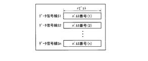
- the correction pulse specifying circuit 22 specifies which of 2 r correction pulses is used for each data signal line. More specifically, as shown in FIG. 10, the correction pulse specifying circuit 22 stores the number of correction pulses to be used (hereinafter referred to as pulse number Zj) among 2 r correction pulses for each data signal line Sj. is doing.
- One pulse number is represented by r bits, and the total data amount of the pulse numbers stored in the correction pulse designating circuit 22 is (n ⁇ r) bits.
- the pulse number is determined by measuring the display gradation of the liquid crystal panel 2 and is stored in the correction pulse designating circuit 22 so as to be rewritable.
- the correction pulse designating circuit 22 outputs n pulse numbers Z1 to Zn in accordance with the output mode of the gradation data X1 to Xn.
- the correction pulse designating circuit 22 outputs the pulse number Zi to the charge / discharge control circuit 23a and the pulse number Zi + 1 to the charge / discharge control circuit 23b during the first writing. Further, the correction pulse designating circuit 22 outputs the pulse number Zi + 1 to the charge / discharge control circuit 23a and the pulse number Zi to the charge / discharge control circuit 23b at the time of the second writing.
- FIG. 7 shows a state at the time of the first writing.
- the charge / discharge control circuit 23 a outputs the control signal ZC, the PWM pattern selected by the selector 15 a, 2 r correction pulses PL generated by the correction pulse generation circuit 21, and the correction pulse designation circuit 22.
- the pulse number (r bit) is input.
- the charge / discharge control circuit 23a includes a selector (not shown). This selector selects one correction pulse from 2 r correction pulses PL using the pulse number as a selection control signal.
- a correction charging period a period in which the selected correction pulse is at a high level.
- the charge / discharge control circuit 23a controls the charge / discharge circuit 17a based on the internally selected correction pulse, the control signal ZC, and the PWM pattern selected by the selector 15a.
- the charge / discharge control circuit 23a controls the transistor 171 to be in the on state and the transistor 172 to be in the off state during the charging period and the correction charging period. At this time, the charge / discharge circuit 17a outputs the positive charge voltage VP.
- the charge / discharge control circuit 23a controls the transistor 171 to be off and the transistor 172 to be on during the discharge period. At this time, the charge / discharge circuit 17a outputs a discharge voltage (ground voltage). In the voltage holding period excluding the correction charging period, the charge / discharge control circuit 23a controls both the transistors 171 and 172 to the off state. At this time, the output of the charge / discharge circuit 17a is in a high impedance state.
- the charge / discharge control circuit 23b outputs the control signal ZC, the PWM pattern selected by the selector 15b, 2 r correction pulses PL generated by the correction pulse generation circuit 21, and the correction pulse designation circuit 22 The pulse number is entered.
- Charge and discharge control circuit 23b like the discharge control circuit 23a, by using the selector selects one of the correction pulse from the 2 r pieces of correction pulse PL.
- the charge / discharge control circuit 23b controls the charge / discharge circuit 17b based on the internally selected correction pulse, the control signal ZC, and the PWM pattern selected by the selector 15b.
- the charge / discharge control circuit 23b controls the transistor 173 to be in an off state and the transistor 174 to be in an on state during the charge period and the correction charge period. At this time, the charge / discharge circuit 17b outputs the negative charge voltage VM.
- the charge / discharge control circuit 23b controls the transistor 173 to be on and the transistor 174 to be off during the discharge period. At this time, the charge / discharge circuit 17b outputs a discharge voltage (ground voltage). In the voltage holding period excluding the correction charging period, the charge / discharge control circuit 23b controls both the transistors 173 and 174 to the off state. At this time, the output of the charge / discharge circuit 17b is in a high impedance state.
- charge and discharge control circuit 23a, 23b is selected from among 2 r pieces of correction pulses generated by the correction pulse generating circuit 21, one correction pulse based on the pulse number specified for each data signal line Then, based on the selected correction pulse, the charge control signal supplied to the transistors 171 and 174 is changed to a level instructing charging.
- the output voltages of the charge / discharge circuits 17 a and 17 b are output to the outside of the data signal line drive circuit 20 via the polarity selection circuit 18.
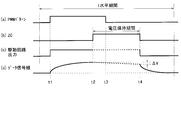
- the output voltage of the data signal line driving circuit 20 changes as shown in FIG. FIG. 8D shows a change in the output voltage of the data signal line drive circuit 20 when the correction pulse PL1 is selected.
- the output voltage of the data signal line driving circuit 20 changes to VP at time t1 and changes to zero at time t4.
- the output of the data signal line driving circuit 20 is in a high impedance state from time t2 to t51 and from time t6 to t4. As described above, the output voltage of the data signal line driving circuit 20 becomes equal to the positive charging voltage VP from time t51 to time t6.
- the voltage of the data signal line Si changes as shown in FIG. FIG. 8E shows changes in the voltage of the data signal line Si when the correction pulse PL1 is selected.
- the voltage of the data signal line Si starts increasing at time t1, and stops increasing at time t2.
- the voltage of the data signal line Si is constant after time t2.
- a leakage current flows through the data signal line Si.
- the voltage of the data signal line Si gradually decreases after time t2.
- a correction charging period is provided near the end of the voltage holding period.
- the data signal line drive circuit 20 outputs the same voltage as in the charging period, and the potential of the data signal line is corrected.
- the potential of the data signal line is corrected.
- FIG. It rises again from t51 to t6 and reaches the same level as time t2 at time t4.
- the data signal line driving circuit 20 generates a plurality of types of correction pulses PL having a predetermined width, and selects which correction pulse is used for each data signal line. To do. Thus, even when the voltage of the data signal line changes due to the leakage current, the correction can be performed using a suitable correction pulse, and the data signal line can be driven accurately.
- the liquid crystal display device according to the third embodiment of the present invention has the same configuration as the liquid crystal display device 1 (FIG. 1) according to the first embodiment.
- the liquid crystal display device according to the third embodiment includes a data signal line drive circuit 30 shown in FIG. 12 instead of the data signal line drive circuit 10.
- the same constituent elements as those in the first and second embodiments are denoted by the same reference numerals and description thereof is omitted.
- FIG. 12 is a diagram showing a configuration of the data signal line driving circuit 30.
- the data signal line drive circuit 30 includes a transistor designation circuit 31 added to the data signal line drive circuit 20 according to the second embodiment, and charge / discharge control circuits 23a and 23b and a charge / discharge circuit 17a. 17b is replaced with charge / discharge control circuits 32a, 32b and charge / discharge circuits 33a, 33b, respectively.
- the data register 11, the PWM pattern generation circuit 12, and the PWM pattern designation circuit 14 are omitted.
- the charge / discharge circuit 33a is a CMOS switch in which a plurality of P-type transistors 331 are connected in parallel and an N-type transistor 172 is connected in series thereto.
- the positive charging voltage VP is fixedly applied to the source terminals of all the transistors 331, and the source terminals of the transistors 172 are grounded.
- the charge / discharge circuit 33a outputs the drain terminal voltages of the transistors 331 and 172.
- the charge / discharge circuit 33b is a CMOS switch in which a plurality of N-type transistors 334 are connected in parallel and a P-type transistor 173 is connected in series thereto.
- the source terminal of the transistor 173 is grounded, and the negative charging voltage VM is fixedly applied to the source terminals of all the transistors 334.
- the charge / discharge circuit 33b outputs the drain terminal voltages of the transistors 173 and 334.
- the plurality of transistors 331 those having different sizes and those controlled using the same control signal are included.
- the plurality of transistors 331 are controlled using s control signals in total (s is an integer of 2 or more), and the plurality of transistors 334 is the same as this.
- the transistor designating circuit 31 designates which of the plurality of transistors 331 and 334 is to be used for each data signal line according to the temperature. More specifically, as shown in FIG. 13, the transistor designating circuit 31 has data (hereinafter, referred to as “transistor”) that designates a transistor to be used from among the plurality of transistors 331 and 334 for each data signal line Sj and f temperature ranges. Transistor designation information Uj). The transistor to be used is specified using a control signal given to the gate terminal. One piece of transistor designation information is represented by s bits, and the total data amount of the transistor designation information stored in the transistor designation circuit 31 is (n ⁇ f ⁇ s) bits. The transistor designation information is determined, for example, by measuring the display gradation of the liquid crystal panel 2 and is stored in the transistor designation circuit 31 in a rewritable manner.
- the transistor designating circuit 31 receives a temperature T detected by a temperature sensor (not shown) provided in the liquid crystal display device.
- the transistor designation circuit 31 obtains the temperature range to which the temperature T belongs from the f temperature ranges, and outputs n pieces of transistor designation information U1 to Un corresponding to the obtained temperature range in parallel.
- the transistor designating circuit 31 outputs n pieces of transistor designating information U1 to Un in accordance with the output mode of the gradation data X1 to Xn.
- the transistor designation circuit 31 outputs transistor designation information Ui to the charge / discharge control circuit 32a and outputs transistor designation information Ui + 1 to the charge / discharge control circuit 32b during the first writing.
- the transistor designation circuit 31 outputs transistor designation information Ui + 1 to the charge / discharge control circuit 32a and outputs transistor designation information Ui to the charge / discharge control circuit 32b during the second writing.
- FIG. 12 shows a state at the time of the first writing.
- the charge / discharge control circuit 32 a outputs the control signal ZC, the PWM pattern selected by the selector 15 a, 2 r correction pulses PL generated by the correction pulse generation circuit 21, and the correction pulse designation circuit 22.
- transistor designation information (s bit) output from the transistor designation circuit 31 is input.
- the charge / discharge control circuit 32a controls one or more transistors designated by the transistor designation information among a plurality of transistors 331 to be in an on state and the remaining transistors 331 and 172 to be in an off state during the charge period and the correction charge period. To do. At this time, the charge / discharge circuit 33a outputs the positive charge voltage VP.
- the charge / discharge control circuit 32a controls all the transistors 331 to be off and the transistor 172 to be on during the discharge period. At this time, the charge / discharge circuit 33a outputs a discharge voltage (ground voltage). In the voltage holding period, the charge / discharge control circuit 32a controls all the transistors 331 and 172 to be in an off state. At this time, the output of the charge / discharge circuit 33a is in a high impedance state.
- the charge / discharge control circuit 32b outputs the control signal ZC, the PWM pattern selected by the selector 15b, 2 r correction pulses PL generated by the correction pulse generation circuit 21, and the correction pulse designation circuit 22 In addition to the pulse number, transistor designation information output from the transistor designation circuit 31 is input.
- the charge / discharge control circuit 32b controls one or more transistors designated by the transistor designation information among the plurality of transistors 334 to be in an on state and the remaining transistors 334 and 173 to be in an off state during the charge period and the correction charge period. To do.
- the charge / discharge circuit 33b outputs the negative charge voltage VM.
- the charge / discharge control circuit 32b controls the transistor 173 to be on and all the transistors 334 to be off during the discharge period.
- the charge / discharge circuit 33b outputs a discharge voltage (ground voltage).
- the charge / discharge control circuit 32b controls the transistor 173 and all the transistors 334 to be turned off. At this time, the output of the charge / discharge circuit 33b is in a high impedance state.
- the impedance of a transistor included in the charge / discharge circuit of the data signal line driving circuit varies greatly depending on the temperature. For this reason, in the data signal line driving circuit that performs pulse width modulation driving, the ultimate voltage of the data signal line varies with temperature. Therefore, the data signal line may not be driven accurately when the temperature changes.
- the data signal line driving circuit 30 includes charge / discharge circuits 33a and 33b including a plurality of charging transistors, and which of the charging transistors is used is determined by the data signal line. Each Sj is selected according to the temperature. As a result, even when the characteristics of the charging transistor fluctuate with changes in temperature, the data signal line can be accurately driven using a suitable charging transistor.
- the data signal line drive circuit 30 shown in FIG. 12 is obtained by adding a temperature correction function to the data signal line drive circuit 20 according to the second embodiment, but the data signal line drive according to the first embodiment.
- a temperature correction function may be added to the circuit 10.
- the liquid crystal display device according to the fourth embodiment of the present invention has the same configuration as the liquid crystal display device 1 (FIG. 1) according to the first embodiment.
- the liquid crystal display device according to the fourth embodiment further includes a counter electrode drive circuit (not shown) for driving the counter electrode of the liquid crystal panel 2, and instead of the data signal line drive circuit 10, the data signal shown in FIG. A line drive circuit 40 is provided.
- the same constituent elements as those of the first embodiment are denoted by the same reference numerals and description thereof is omitted.
- the one-line inversion driving for inverting the polarity of the gradation voltage to be written in the pixel circuit 5 for each row, and the voltage applied to the counter electrode of the liquid crystal panel 2 relative to a relatively low level. Opposite inversion driving to switch to a higher level.
- writing a positive voltage to the pixel circuit 5 by applying a low level voltage to the counter electrode of the liquid crystal panel 2 is referred to as first writing, and applying a high level voltage to the counter electrode of the liquid crystal panel 2 causes the pixel to be written.
- Writing the negative voltage to the circuit 5 is called second writing.
- FIG. 14 is a diagram showing a configuration of the data signal line driving circuit 40.
- the data signal line drive circuit 40 includes a data register 11, a PWM pattern generation circuit 12, a control signal generation circuit 13, a PWM pattern designation circuit 14, n selectors 41, and n charge / discharge control circuits. 42 and n charging / discharging circuits 43 are included.
- the selector 41, the charge / discharge control circuit 42, and the charge / discharge circuit 43 are provided one by one corresponding to the data signal line Sj, and the gradation data Xj output from the data register 11 is output to the data signal line Sj.
- a grayscale voltage corresponding to is applied.
- the selector 41 includes 2 p + q positive side PWM patterns PTP, 2 p + q negative side PWM patterns PTM, gradation data (p bits) output from the data register 11, and PWM pattern designation.
- the pattern set number (q bits) output from the circuit 14 and the polarity control signal PC1 are input.
- the selector 41, the gradation data, pattern group number, and, as a selection control signal the polarity control signal PC1, among the 2 p + q pieces of positive PWM pattern PTP and 2 p + q pieces of negative PWM pattern PTM 1 PWM pattern is selected.
- the charge / discharge circuit 43 is a CMOS switch in which a P-type transistor 431 and an N-type transistor 432 are connected in series like the charge / discharge circuit 17a.
- the voltage VP is fixedly applied to the source terminal of the transistor 431, and the source terminal of the transistor 432 is grounded.
- the charge / discharge circuit 43 outputs the drain terminal voltages of the transistors 431 and 432.
- the charge / discharge control circuit 42 controls the charge / discharge circuit 43 based on the control signal ZC, the polarity control signal PC1 and the PWM pattern selected by the selector 41. More specifically, the charge / discharge control circuit 42 obtains a first control signal to be given to the gate terminal of the transistor 431 and a second control signal to be given to the gate terminal of the transistor 432 based on the three given signals. The charge / discharge control circuit 42 controls the transistor 431 to be in an on state and the transistor 432 to be in an off state during a charging period at the time of first writing and a discharging period after the first writing. At this time, the charge / discharge circuit 43 outputs the voltage VP.
- the charge / discharge control circuit 42 controls the transistor 431 to be in an off state and the transistor 432 to be in an on state in a charging period at the time of second writing and a discharging period after the second writing. At this time, the charge / discharge circuit 43 outputs a ground voltage. In the voltage holding period, the charge / discharge control circuit 42 controls both the transistors 431 and 432 to be in an off state. At this time, the output of the charge / discharge circuit 43 is in a high impedance state.
- FIG. 15 is a signal waveform diagram of the data signal line driving circuit 40.
- first period a period from when the control signal ZC changes to the low level within the horizontal period during which the second writing is performed until the control signal ZC changes to the low level within the horizontal period during which the first writing is performed.
- second period The period from when the control signal ZC changes to low level within the horizontal period during which the first writing is performed until when the control signal ZC changes to low level within the horizontal period during which the second writing is performed.
- a period during which the PWM pattern is at a high level and the control signal ZC is at a low level within the first period is a charging period at the time of first writing.
- a period in which the PWM pattern and the control signal ZC are at a low level within the second period is a discharge period after the first writing.
- a period in which the PWM pattern is at a high level and the control signal ZC is at a low level within the second period is a charging period at the time of second writing.
- a period in which the PWM pattern and the control signal ZC are at a low level within the first period is a discharge period after the second writing.
- time t14 to t24 is a charging period at the time of the first writing
- time t44 to t15 is a discharging period after the first writing.
- the time t15 to t25 is the charging period at the time of the second writing
- the time t45 to t16 is the discharging period after the second writing.
- the voltage of the data signal line Si starts to rise at time t14, stops rising at time t24, becomes almost constant from time t24 to t44, starts to rise again at time t44, and reaches the voltage VP by time t15 at the latest.
- the voltage of the data signal line Si starts to decrease at time t15, stops decreasing at time t25, becomes almost constant at times t25 to t45, starts decreasing again at time t45, and is not later than time t16. It becomes zero.
- the voltage of the data signal line Si further rises and finally becomes equal to the voltage VP.
- the voltage of the data signal line Si further decreases and finally becomes zero. Therefore, when the second write is performed after the first write, the voltage of the data signal line Si is changed from the voltage VP to reach a desired level, and when the first write is performed after the second write, the data The voltage of the signal line Si can be changed from zero to reach a desired level.
- the first control signal for controlling the transistor 431 is a charge control signal in the first period and a discharge control signal in the second period.
- the second control signal for controlling the transistor 432 is a discharge control signal in the first period, and a charge control signal in the second period.
- the transistor 431 functions as a charging transistor or a discharging transistor in accordance with the first control signal.
- the transistor 432 functions as a charging transistor or a discharging transistor in accordance with the second control signal.
- the method of the first embodiment is applied when the line inversion driving and the counter inversion driving are performed.
- the method of the second or third embodiment is used.
- a method may be applied.
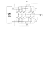
- a charge / discharge circuit 51 shown in FIG. 16 is used.
- the charge / discharge circuit 51 is a CMOS switch in which a circuit in which a plurality of P-type transistors 511 are connected in parallel and a circuit in which a plurality of N-type transistors 512 are connected in parallel are connected in series.
- the charging / discharging circuit 51 includes a plurality of transistors 511 and 512, and in the charging period at the time of the first writing, one or more specified from the plurality of transistors 511 according to the temperature for each data signal line Sj.
- the plurality of transistors 512 one or more transistors designated according to the temperature are used for each data signal line Sj in the charging period at the time of the second writing using the transistors. Thereby, even when the temperature changes, the data signal line Sj can be accurately driven using a suitable charging transistor for each data signal line Sj.
- the PWM pattern generation circuit 12 generates a PWM pattern that becomes a high level once in one horizontal period.
- the PWM pattern generation circuit may generate a PWM pattern that becomes a high level at least twice in one horizontal period.
- the PWM pattern generation circuit stores one or more sets of change timings to high level and low level for each PWM pattern in addition to the on-timing shown in FIG.
- the change in the voltage of the data signal line can be controlled more accurately, and the data signal line can be driven more accurately.
- the number of changes in the PWM pattern is small.
- the present invention can also be applied to various display devices that perform gradation display.
- the power consumption can be reduced by performing pulse width modulation driving, and the data signal line can be accurately driven by performing various corrections. it can. Further, according to the display device of the present invention, gradation can be accurately displayed using the data signal line driving circuit of the present invention.
- the drive circuit of the present invention has a feature that the data signal line can be accurately driven using pulse width modulation drive, it can be used for drive circuits of various display devices such as liquid crystal display devices.
Landscapes
- Engineering & Computer Science (AREA)
- Chemical & Material Sciences (AREA)
- Crystallography & Structural Chemistry (AREA)
- Physics & Mathematics (AREA)
- Computer Hardware Design (AREA)
- General Physics & Mathematics (AREA)
- Theoretical Computer Science (AREA)
- Control Of Indicators Other Than Cathode Ray Tubes (AREA)
Abstract
本願発明は、パルス幅変調駆動でデータ信号線を正確に駆動し、階調を正確に表示することを目的とする。 PWMパターン生成回路(12)は、階調と階調電圧の極性の組合せに対応したPWMパターンを2q 組生成する。セレクタ(15)は、階調データとパターン組番号に基づき、2p+q 個のPWMパターンの中から1個のPWMパターンを選択する。充放電制御回路(16)は、選択されたPWMパターンに基づき、データ信号線に充電電圧と放電電圧を切り替えて印加するよう充放電回路(17)を制御する。複数種類生成した補正パルスの中からデータ信号線ごとに1個の補正パルスを選択し、これに基づきデータ信号線に充電電圧を印加してもよい。充電用トランジスタを複数個設け、温度に応じてデータ信号線ごとに使用する充電用トランジスタを指定してもよい。
Description
本発明は、液晶表示装置などの表示装置に関し、特に、表示装置のデータ信号線を駆動する駆動回路および駆動方法に関する。
液晶表示装置は、薄型、低消費電力という特徴を有し、様々な用途に利用されている。液晶表示装置は、例えば、バッテリーで動作する携帯機器にも利用されている。近年では、携帯機器の表示画面でも大画面化と高解像度化が進んでいる。大画面化と高解像度化が進むと、液晶パネルの駆動回路の負荷は大きくなり、駆動回路の動作周波数は高くなる。このため、液晶表示装置の消費電力は増大する。そこで、携帯機器のバッテリーサイズを抑えるために、液晶表示装置にはさらなる低消費電力化が要求されている。
液晶表示装置の消費電力は、液晶パネルの消費電力(充放電による消費電力)と駆動回路の消費電力とに大別される。以下、駆動回路の消費電力を削減する方法を検討する。駆動回路の消費電力は、回路構成を工夫することにより削減することができる。例えば、定常電流が流れるアナログ回路を減らすことにより、駆動回路の消費電力を削減することができる。
従来の一般的な液晶表示装置は、アナログバッファ回路を含む駆動回路を用いて、データ信号線(映像信号線、ソースバスラインなどとも呼ばれる)を駆動する。アナログバッファ回路には定常電流が流れるので、アナログバッファ回路は液晶表示装置の消費電力を増大させる要因となる。そこで、アナログバッファ回路を用いずにデータ信号線を駆動する方法として、データ信号線に対して2種類の電圧(充電電圧と放電電圧)だけを切り替えて印加し、2種類の電圧を印加する時間の長さを映像信号に応じて変化させる方法(以下、パルス幅変調駆動という)が、従来から知られている。
パルス幅変調駆動に関して、特許文献1には、データ信号線に印加する電圧に満たない電圧を画素に書き込む方法や、走査信号線とデータ信号線の波形をずらすことにより階調を表示し、データ信号線方向の画素の極性を1つおきに反転させる方法が記載されている。特許文献2には、パルス幅変調駆動を行うときに、正極性書き込み時と負極性書き込み時とで、走査信号線の電圧とデータ信号線の電圧との差を等しくする方法が記載されている。特許文献3には、パルス幅変調駆動以外のデータ信号線の駆動方法として、1水平期間中に振動する振動成分を有する電圧をデータ信号線に印加する方法が記載されている。
パルス幅変調駆動を行うことにより、データ信号線駆動回路に含まれるアナログバッファ回路を削除して、表示装置の消費電力を削減することができる。しかしながら、一般に、データ信号線の充電時の時定数にはばらつきがある。このため、2本のデータ信号線に充電電圧を同じ時間だけ印加しても、データ信号線の到達電圧に差が生じることがある。この差は、表示画面では輝度差となる。このようにパルス幅変調駆動には、データ信号線の充電時の時定数にばらつきがある場合には、データ信号線を正確に駆動できないという問題がある。データ信号線の本数や階調数が多い表示装置では、この問題は顕著になる。
特許文献1および2には、この問題の解決方法は記載されていない。また、特許文献3に記載された方法では、データ信号線の電圧を振動させるので、負荷容量に対する充放電が頻繁に行われ、無駄な電力が消費される。また、特許文献3に記載された方法には、階調数が多い表示装置には対応できないという問題もある。
それ故に、本発明は、パルス幅変調駆動を用いてデータ信号線を正確に駆動する駆動回路、および、これを用いて階調を正確に表示する表示装置を提供することを目的とする。
本発明の第1の局面は、表示装置のデータ信号線を駆動する駆動回路であって、
階調に応じたパルス幅を有するパターンを各階調について複数組生成するパターン生成回路と、
前記データ信号線ごとに与えられた階調データと前記データ信号線ごとに指定されたパターンの組とに基づき、前記パターン生成回路で生成されたパターンの中から1個のパターンを選択する選択回路と、
前記選択回路で選択されたパターンに基づき、充電制御信号と放電制御信号を求める充放電制御回路と、
前記充電制御信号と前記放電制御信号に従い、前記データ信号線に充電電圧と放電電圧を切り替えて印加する充放電回路とを備える。
階調に応じたパルス幅を有するパターンを各階調について複数組生成するパターン生成回路と、
前記データ信号線ごとに与えられた階調データと前記データ信号線ごとに指定されたパターンの組とに基づき、前記パターン生成回路で生成されたパターンの中から1個のパターンを選択する選択回路と、
前記選択回路で選択されたパターンに基づき、充電制御信号と放電制御信号を求める充放電制御回路と、
前記充電制御信号と前記放電制御信号に従い、前記データ信号線に充電電圧と放電電圧を切り替えて印加する充放電回路とを備える。
本発明の第2の局面は、本発明の第1の局面において、
前記充放電回路は、前記充電制御信号に従い前記データ信号線に前記充電電圧を印加する充電用トランジスタと、前記放電制御信号に従い前記データ信号線に前記放電電圧を印加する放電用トランジスタとを含むことを特徴とする。
前記充放電回路は、前記充電制御信号に従い前記データ信号線に前記充電電圧を印加する充電用トランジスタと、前記放電制御信号に従い前記データ信号線に前記放電電圧を印加する放電用トランジスタとを含むことを特徴とする。
本発明の第3の局面は、本発明の第2の局面において、
所定の幅を有する補正パルスを複数種類生成する補正パルス生成回路をさらに備え、
前記充放電制御回路は、前記補正パルス生成回路で生成された補正パルスの中から前記データ信号線ごとに指定された1個の補正パルスを選択し、選択した補正パルスに基づき、前記充電制御信号を充電を指示するレベルに変化させることを特徴とする。
所定の幅を有する補正パルスを複数種類生成する補正パルス生成回路をさらに備え、
前記充放電制御回路は、前記補正パルス生成回路で生成された補正パルスの中から前記データ信号線ごとに指定された1個の補正パルスを選択し、選択した補正パルスに基づき、前記充電制御信号を充電を指示するレベルに変化させることを特徴とする。
本発明の第4の局面は、本発明の第2の局面において、
前記充放電回路は、前記充電用トランジスタを複数個含み、充電時には、前記複数の充電用トランジスタの中から、前記データ信号線ごとに温度に応じて指定された1個以上のトランジスタを使用することを特徴とする。
前記充放電回路は、前記充電用トランジスタを複数個含み、充電時には、前記複数の充電用トランジスタの中から、前記データ信号線ごとに温度に応じて指定された1個以上のトランジスタを使用することを特徴とする。
本発明の第5の局面は、本発明の第2の局面において、
前記充放電制御回路は、1水平期間内に設定された電圧保持期間では、前記充電用トランジスタと前記放電用トランジスタを共にオフ状態に制御することを特徴とする。
前記充放電制御回路は、1水平期間内に設定された電圧保持期間では、前記充電用トランジスタと前記放電用トランジスタを共にオフ状態に制御することを特徴とする。
本発明の第6の局面は、本発明の第2の局面において、
前記充放電制御回路は、第1期間では前記充電制御信号であり、第2期間では前記放電制御信号である第1制御信号と、第1期間では前記放電制御信号であり、第2期間では前記充電制御信号である第2制御信号とを出力し、
前記充放電回路は、前記第1制御信号に従い前記充電用トランジスタまたは前記放電用トランジスタとして機能する第1トランジスタと、前記第2制御信号に従い前記放電用トランジスタまたは前記充電用トランジスタとして機能する第2トランジスタとを含むことを特徴とする。
前記充放電制御回路は、第1期間では前記充電制御信号であり、第2期間では前記放電制御信号である第1制御信号と、第1期間では前記放電制御信号であり、第2期間では前記充電制御信号である第2制御信号とを出力し、
前記充放電回路は、前記第1制御信号に従い前記充電用トランジスタまたは前記放電用トランジスタとして機能する第1トランジスタと、前記第2制御信号に従い前記放電用トランジスタまたは前記充電用トランジスタとして機能する第2トランジスタとを含むことを特徴とする。
本発明の第7の局面は、本発明の第6の局面において、
前記充放電回路は、前記第1および第2トランジスタを複数個ずつ含み、第1期間内の充電時には、前記複数の第1トランジスタの中から、前記データ信号線ごとに温度に応じて指定された1個以上のトランジスタを使用し、第2期間内の充電時には、前記複数の第2トランジスタの中から、前記データ信号線ごとに温度に応じて指定された1個以上のトランジスタを使用することを特徴とする。
前記充放電回路は、前記第1および第2トランジスタを複数個ずつ含み、第1期間内の充電時には、前記複数の第1トランジスタの中から、前記データ信号線ごとに温度に応じて指定された1個以上のトランジスタを使用し、第2期間内の充電時には、前記複数の第2トランジスタの中から、前記データ信号線ごとに温度に応じて指定された1個以上のトランジスタを使用することを特徴とする。
本発明の第8の局面は、本発明の第1の局面において、
前記データ信号線の1水平期間内での充電時間は、前記データ信号線の充電時の時定数の2倍以下であることを特徴とする。
前記データ信号線の1水平期間内での充電時間は、前記データ信号線の充電時の時定数の2倍以下であることを特徴とする。
本発明の第9の局面は、本発明の第1の局面において、
前記データ信号線の1水平期間内での充電時間は、前記データ信号線の充電時の時定数の2.3倍以下であることを特徴とする。
前記データ信号線の1水平期間内での充電時間は、前記データ信号線の充電時の時定数の2.3倍以下であることを特徴とする。
本発明の第10の局面は、本発明の第1の局面において、
1水平期間が前記データ信号線の充電時の時定数の4.5倍以上であることを特徴とする。
1水平期間が前記データ信号線の充電時の時定数の4.5倍以上であることを特徴とする。
本発明の第11の局面は、階調表示を行う表示装置であって、
複数の走査信号線と複数のデータ信号線と複数の画素回路とを含む表示パネルと、
前記走査信号線を順に選択する走査信号線駆動回路と、
前記データ信号線に対して映像信号に応じた階調電圧を印加するデータ信号線駆動回路とを備え、
前記データ信号線駆動回路は、
階調に応じたパルス幅を有するパターンを各階調について複数組生成するパターン生成回路と、
前記データ信号線ごとに与えられた階調データと前記データ信号線ごとに指定されたパターンの組とに基づき、前記パターン生成回路で生成されたパターンの中から1個のパターンを選択する選択回路と、
前記選択回路で選択されたパターンに基づき、充電制御信号と放電制御信号を求める充放電制御回路と、
前記充電制御信号と前記放電制御信号に従い、前記データ信号線に充電電圧と放電電圧を切り替えて印加する充放電回路とを含むことを特徴とする。
複数の走査信号線と複数のデータ信号線と複数の画素回路とを含む表示パネルと、
前記走査信号線を順に選択する走査信号線駆動回路と、
前記データ信号線に対して映像信号に応じた階調電圧を印加するデータ信号線駆動回路とを備え、
前記データ信号線駆動回路は、
階調に応じたパルス幅を有するパターンを各階調について複数組生成するパターン生成回路と、
前記データ信号線ごとに与えられた階調データと前記データ信号線ごとに指定されたパターンの組とに基づき、前記パターン生成回路で生成されたパターンの中から1個のパターンを選択する選択回路と、
前記選択回路で選択されたパターンに基づき、充電制御信号と放電制御信号を求める充放電制御回路と、
前記充電制御信号と前記放電制御信号に従い、前記データ信号線に充電電圧と放電電圧を切り替えて印加する充放電回路とを含むことを特徴とする。
本発明の第12の局面は、表示装置のデータ信号線を駆動する駆動方法であって、
階調に応じたパルス幅を有するパターンを各階調について複数組生成するステップと、
前記データ信号線ごとに与えられた階調データと前記データ信号線ごとに指定されたパターンの組とに基づき、生成されたパターンの中から1個のパターンを選択するステップと、
選択されたパターンに基づき、充電制御信号と放電制御信号を求めるステップと、
前記充電制御信号と前記放電制御信号に従い、前記データ信号線に充電電圧と放電電圧を切り替えて印加するステップとを備える。
階調に応じたパルス幅を有するパターンを各階調について複数組生成するステップと、
前記データ信号線ごとに与えられた階調データと前記データ信号線ごとに指定されたパターンの組とに基づき、生成されたパターンの中から1個のパターンを選択するステップと、
選択されたパターンに基づき、充電制御信号と放電制御信号を求めるステップと、
前記充電制御信号と前記放電制御信号に従い、前記データ信号線に充電電圧と放電電圧を切り替えて印加するステップとを備える。
本発明の第13の局面は、複数の走査信号線と複数のデータ信号線と複数の画素回路とを有する表示パネルを有し、階調表示を行う表示装置の駆動方法であって、
前記走査信号線を順に選択するステップと、
階調に応じたパルス幅を有するパターンを各階調について複数組生成するステップと、
前記データ信号線ごとに与えられた階調データと前記データ信号線ごとに指定されたパターンの組とに基づき、生成されたパターンの中から1個のパターンを選択するステップと、
選択されたパターンに基づき、充電制御信号と放電制御信号を求めるステップと、
前記充電制御信号と前記放電制御信号に従い、前記データ信号線に充電電圧と放電電圧を切り替えて印加するステップとを備える。
前記走査信号線を順に選択するステップと、
階調に応じたパルス幅を有するパターンを各階調について複数組生成するステップと、
前記データ信号線ごとに与えられた階調データと前記データ信号線ごとに指定されたパターンの組とに基づき、生成されたパターンの中から1個のパターンを選択するステップと、
選択されたパターンに基づき、充電制御信号と放電制御信号を求めるステップと、
前記充電制御信号と前記放電制御信号に従い、前記データ信号線に充電電圧と放電電圧を切り替えて印加するステップとを備える。
本発明の第1または第12の局面によれば、各階調に対応したパターンを複数組生成し、いずれの組のパターンを使用するかをデータ信号線ごとに選択する。これにより、データ信号線の充電時の時定数にばらつきがある場合でも、データ信号線ごとに好適なパターンを用いてデータ信号線を正確に駆動することができる。
本発明の第2の局面によれば、充電用トランジスタと放電用トランジスタを用いて、データ信号線に充電電圧と放電電圧を切り替えて印加する充放電回路を構成することができる。
本発明の第3の局面によれば、補正パルスを複数種類生成し、いずれの補正パルスを使用するかをデータ信号線ごとに選択する。これにより、リーク電流によってデータ信号線の電圧が変化する場合でも、データ信号線ごとに好適な補正パルスを用いて補正を行い、データ信号線を正確に駆動することができる。
本発明の第4の局面によれば、充電用トランジスタを複数個設け、いずれの充電用トランジスタを使用するかをデータ信号線ごとに温度に応じて選択する。これにより、温度が変化したときでも、データ信号線ごとに好適な充電用トランジスタを用いてデータ信号線を正確に駆動することができる。
本発明の第5の局面によれば、1水平期間内に電圧保持期間を設けることにより、データ信号線の電圧をデータ信号線に接続された画素回路に確実に書き込むことができる。
本発明の第6の局面によれば、第1および第2トランジスタを用いて、データ信号線に充電電圧と放電電圧を切り替えて印加する充放電回路を構成することができる。
本発明の第7の局面によれば、第1および第2トランジスタを複数個ずつ設け、充電用トランジスタとしていずれのトランジスタを使用するかをデータ信号線ごとに温度に応じて選択する。これにより、温度が変化したときでも、データ信号線ごとに好適な充電用トランジスタを用いてデータ信号線を正確に駆動することができる。
本発明の第8または第9の局面によれば、データ信号線の1水平期間内での充電時間をデータ信号線の充電時の時定数の2倍あるいは2.3倍以下にすることにより、無駄な充電時間を削減して、時間を有効に活用することができる。
本発明の第10の局面によれば、1水平期間をデータ信号線の充電時の時定数の4.5倍以上にすることにより、1水平期間内にデータ信号線の電圧を複数のレベルに到達させるために十分な時間を確保することができる。
本発明の第11または第13の局面によれば、データ信号線を正確に駆動できる駆動回路または駆動方法を用いて、階調を正確に表示することができる。
(第1の実施形態)
図1は、本発明の第1の実施形態に係る液晶表示装置の構成を示すブロック図である。図1に示す液晶表示装置1は、液晶パネル2、表示制御回路3、走査信号線駆動回路4、および、データ信号線駆動回路10を備えている。液晶表示装置1は、表示制御回路3から出力された映像信号Xに基づき、2p レベル(pは2以上の整数)の階調表示を行う。以下、mは1以上の整数、nは2以上の偶数、iは1以上n以下の奇数、jは1以上n以下の整数であるとする。
図1は、本発明の第1の実施形態に係る液晶表示装置の構成を示すブロック図である。図1に示す液晶表示装置1は、液晶パネル2、表示制御回路3、走査信号線駆動回路4、および、データ信号線駆動回路10を備えている。液晶表示装置1は、表示制御回路3から出力された映像信号Xに基づき、2p レベル(pは2以上の整数)の階調表示を行う。以下、mは1以上の整数、nは2以上の偶数、iは1以上n以下の奇数、jは1以上n以下の整数であるとする。
液晶パネル2は、m本の走査信号線G1~Gm、n本のデータ信号線S1~Sn、および、(m×n)個の画素回路5を含んでいる。走査信号線G1~Gmは、互いに平行に配置される。データ信号線S1~Snは、走査信号線G1~Gmと直交するように、互いに平行に配置される。走査信号線G1~Gmとデータ信号線S1~Snは、(m×n)箇所で交差する。(m×n)個の交点に対応して、全部で(m×n)個の画素回路5が配置される。画素回路5は、1本の走査信号線と1本のデータ信号線に接続される。
表示制御回路3は、走査信号線駆動回路4に対してタイミング制御信号TC1を出力し、データ信号線駆動回路10に対してタイミング制御信号TC2と映像信号Xを出力する。タイミング制御信号TC1には、例えば、ゲートスタートパルスやゲートクロックなどが含まれる。タイミング制御信号TC2には、例えば、ソーススタートパルスやソースクロックなどが含まれる。
走査信号線駆動回路4は、タイミング制御信号TC1に基づき、走査信号線G1~Gmを順に選択する。これにより、選択された走査信号線に接続されたn個の画素回路5が、一括して選択される。データ信号線駆動回路10は、タイミング制御信号TC2に基づき、映像信号Xに応じた階調電圧をデータ信号線S1~Snに印加する。これにより、走査信号線駆動回路4によって選択されたn個の画素回路5に、n個の階調電圧が書き込まれる。画素回路5の輝度は、画素回路5に書き込まれた階調電圧によって決まる。走査信号線駆動回路4とデータ信号線駆動回路10を用いて、すべての画素回路5に階調電圧を書き込むことにより、液晶パネル2に画像を表示することができる。
液晶表示装置1は、画素回路5に書き込む階調電圧の極性を隣接する画素回路5ごとに反転させるドット反転駆動を行う。以下、奇数番目(偶数番目)のデータ信号線に接続された画素回路5に正極性電圧(負極性電圧)を書き込むことを第1書き込みといい、奇数番目(偶数番目)のデータ信号線に接続された画素回路5に負極性電圧(正極性電圧)を書き込むことを第2書き込みという。データ信号線駆動回路10は、1水平期間ごとに第1書き込みと第2書き込みを交互に行う。
図2は、データ信号線駆動回路10の構成を示す図である。図2に示すように、データ信号線駆動回路10は、データレジスタ11、PWMパターン生成回路12、制御信号生成回路13、PWMパターン指定回路14、n個のセレクタ15、n個の充放電制御回路16、n個の充放電回路17、および、(n/2)個の極性選択回路18を含んでいる。隣接する2本のデータ信号線Si、Si+1に対応して、2個のセレクタ15a、15b、2個の充放電制御回路16a、16b、2個の充放電回路17a、17b、および、1個の極性選択回路18が設けられる。なお、図2には2本のデータ信号線Si、Si+1を駆動する回路だけが記載されているが、他のデータ信号線を駆動する回路も同様の構造を有する。
表示制御回路3から1水平期間に出力される映像信号Xには、pビットの階調データがn個含まれている。以下、j番目のデータ信号線Sjに対応した階調データをXjという。表示制御回路3は、階調データを1個ずつ順に出力してもよく、階調データを複数個ずつ順に出力してもよい。
データレジスタ11は、表示制御回路3から出力されたn個の階調データX1~Xnを記憶し、1水平期間の間、並列に出力する。より詳細には、データレジスタ11は、(n×p)ビットのレジスタ(図示せず)を2個含んでいる。表示制御回路3から出力されたn個の階調データは、第1レジスタに順に書き込まれる。第1書き込み時には、n個の階調データは、第1レジスタにそのままの順序で書き込まれる。第2書き込み時には、n個の階調データは、第1レジスタに奇数番目と偶数番目を入れ替えて書き込まれる。第1レジスタへの書き込みが完了した後に、n個の階調データは第1レジスタから第2レジスタに一括して転送される。データレジスタ11は、第2レジスタの出力信号を出力する。データレジスタ11は、第1書き込み時にはn個の階調データをX1、X2、X3、X4、…、Xn-1、Xnの順序で出力し、第2書き込み時にはn個の階調データをX2、X1、X4、X3、…、Xn、Xn-1の順序で出力する。なお、図2には第1書き込み時の状態が記載されている。
セレクタ15a、15b、充放電制御回路16a、16b、充放電回路17a、17b、および、極性選択回路18は、データ信号線Si、Si+1に対して、それぞれ、データレジスタ11から出力された階調データXi、Xi+1に応じた階調電圧を印加する。PWMパターン生成回路12、制御信号生成回路13、および、PWMパターン指定回路14は、セレクタ15や充放電制御回路16の動作に必要な信号を出力する。
データ信号線駆動回路10は、データ信号線に対して2種類の電圧(充電電圧と放電電圧)だけを印加し、2種類の電圧を印加する時間の長さを映像信号に応じて変化させるパルス幅変調駆動を行う。データ信号線駆動回路10が行うパルス幅変調駆動は、階調および階調電圧の極性(正極性か負極性か)に対応したPWM(Pulse Width Modulation)パターンを複数組生成し、いずれの組のPWMパターンを使用するかをデータ信号線ごとに選択するという特徴を有する(詳細は後述)。
図3は、データ信号線駆動回路10の信号波形図である。図2および図3を参照して、データ信号線駆動回路10の動作を説明する。PWMパターン生成回路12は、各階調および階調電圧の極性の組合せに対応して、複数のPWMパターンを生成する。PWMパターンには、正極性電圧に対応した正側PWMパターンPTPと、負極性電圧に対応した負側PWMパターンPTMとが含まれる。図3(a)には、階調L1、L2およびL3に対応した3種類の正側PWMパターンが記載されている。データ信号線駆動回路10で生成されるPWMパターンは、1水平期間内の所定時刻で(例えば、階調L1の場合には時刻t11で)ハイレベルに変化し、1水平期間内の時刻t3でローレベルに変化する。PWMパターンのハイレベル期間の長さは、階調および階調電圧の極性に応じて決定される。
制御信号生成回路13は、表示制御回路3から出力されたタイミング制御信号TC2に基づき、制御信号ZCを出力する。図3(b)に示すように、制御信号ZCは、1水平期間内の時刻t2でハイレベルに変化し、1水平期間内の時刻t4でローレベルに変化する。ただし、時刻t2は、PWMパターンがハイレベルに変化する最も遅い時刻よりも後で、時刻t3よりも前である。時刻t4は時刻t3よりも後である。制御信号ZCがローレベルでPWMパターンがハイレベルである期間は、データ信号線に充電電圧を印加する充電期間となる。制御信号ZCとPWMパターンが共にローレベルである期間は、データ信号線に放電電圧を印加する放電期間となる。制御信号ZCがハイレベルである期間は、データ信号線をハイインピーダンス状態にする電圧保持期間となる。電圧保持期間を設けることにより、データ信号線Sjの電圧を画素回路5に確実に書き込むことができる。
第1書き込み時には、データレジスタ11は、セレクタ15aに対して階調データXiを出力し、セレクタ15bに対して階調データXi+1を出力する。セレクタ15aには、階調データXiに加えて、PWMパターン生成回路12で生成された複数の正側PWMパターンPTPが入力される。セレクタ15aは、階調データXiに基づき、複数の正側PWMパターンPTPの中から1個の正側PWMパターンを選択する。セレクタ15bには、階調データXi+1に加えて、PWMパターン生成回路12で生成された複数の負側PWMパターンPTMが入力される。セレクタ15bは、階調データXi+1に基づき、複数の負側PWMパターンPTMの中から1個の負側PWMパターンを選択する。
充放電制御回路16aには、制御信号ZCとセレクタ15aで選択された正側PWMパターンとが入力される。充放電回路17aは、2個のトランジスタ171、172を含むCMOSスイッチである。充放電制御回路16aからの制御によって、充放電回路17aの出力電圧は、充電期間では正側充電電圧VPになり、放電期間で放電電圧(接地電圧)になる。電圧保持期間では、充放電回路17aの出力はハイインピーダンス状態になる。
充放電回路17aの出力電圧は、極性選択回路18を経由して、データ信号線駆動回路10の外部に出力される。データ信号線駆動回路10の出力電圧は、例えば、図3(c)に示すように変化する。図3(c)には、上記3つの階調に対応したデータ信号線駆動回路10の出力電圧の変化が記載されている。例えば階調L1のときには、データ信号線駆動回路10の出力電圧は、時刻t11でVPに変化し、時刻t4でゼロに変化する。ただし、データ信号線駆動回路10の出力は、時刻t2~t4ではハイインピーダンス状態である。
データ信号線Siは、データ信号線駆動回路10の負荷となる。この負荷は、図4に示すように、CR分布定数回路としてモデル化される。データ信号線駆動回路10の出力電圧がステップ状に変化したとき、データ信号線Siの電圧はCR分布定数回路の積分作用によって変化する。このため、データ信号線Siの電圧は、図3(d)に示すように変化する。図3(d)には、上記3つの階調に対応したデータ信号線Siの電圧の変化が記載されている。例えば階調L1のときには、データ信号線Siの電圧は、時刻t11で上昇を開始し、時刻t2で上昇を停止し、時刻t2~t4ではほぼ一定になる。データ信号線Siの電圧は、時刻t4で下降を開始し、やがてゼロに戻る。
充放電制御回路16bには、制御信号ZCとセレクタ15bで選択された負側PWMパターンとが入力される。充放電回路17bは、2個のトランジスタ173、174を含むCMOSスイッチである。充放電制御回路16bからの制御によって、充放電回路17bの出力電圧は、充電期間では負側充電電圧VMになり、放電期間で放電電圧になる。電圧保持期間では、充放電回路17bの出力はハイインピーダンス状態になる。データ信号線駆動回路10の出力電圧とデータ信号線Si+1の電圧は、図3(c)および(d)とは逆方向に変化する。
データ信号線Sjの電圧は、j列目の画素回路5のうち、走査信号線駆動回路4によって選択された画素回路に書き込まれる。上述したように、PWMパターンのハイレベル期間の長さは、階調および階調電圧の極性に応じて決定される。このため、階調に応じてデータ信号線の充電時間が異なり、充電後の電圧(時刻t2における電圧。以下、到達電圧という)も異なる。例えば、図3において階調L1のときには、データ信号線Siは時間T1だけ充電され、到達電圧はV1となる。階調L2(L2<L1)のときには、データ信号線は時間T2(T2<T1)だけ充電され、到達電圧はV2(V2<V1)となる。したがって、階調および階調電圧の極性に応じてPWMパターンのハイレベル期間の長さを好適に決定することにより、映像信号に応じた階調電圧をデータ信号線に印加して階調表示を行うことができる。
以上に述べたパルス幅変調駆動によれば、アナログバッファ回路を用いずにデータ信号線を駆動して、データ信号線の消費電力を削減することができる。しかしながら、一般に、データ信号線の充電時の時定数にはばらつきがある。このため、以上に述べた方法だけでは、データ信号線を正確に駆動することができない。そこで、以下に示すように、本実施形態に係るデータ信号線駆動回路10は、階調と階調電圧の極性の組合せに対応したPWMパターンを複数組使用する。
PWMパターン生成回路12は、1水平期間を周期とし、階調に応じたパルス幅を有するPWMパターンを各階調について複数組生成する。より詳細には、PWMパターン生成回路12は、2q 組(qは1以上の整数)のPWMパターンを生成する。1組のPWMパターンには、2p 個の階調に対応して、2p 個の正側PWMパターンと2p 個の負側PWMパターンとが含まれる。PWMパターン生成回路12は、2p+q 個の正側PWMパターンPTPと、2p+q 個の負側PWMパターンPTMとからなる2p+q+1 個のPWMパターンを出力する。
PWMパターン生成回路12で生成されるPWMパターンは、1水平期間内の異なる時刻でハイレベルに変化し、1水平期間内の同じ時刻でローレベルに変化する。このようなPWMパターンは、ハイレベルへの変化タイミングだけを用いて規定することができる。PWMパターン生成回路12は、図5に示すように、すべてのPWMパターンについて、ハイレベルへの変化タイミング(以下、オンタイミングという)を記憶している。オンタイミングは、例えば、1水平期間の先頭からPWMパターンがハイレベルに変化するまでの時間を所定の精度で表したものである。PWMパターン生成回路12は、オンタイミングを固定的に記憶していてもよく、書き換え可能に記憶していてもよい。
1個のオンタイミングをdビットで表したとき、PWMパターン生成回路12に記憶されるオンタイミングの全体データ量は(2p+q+1 ×d)ビットとなる。PWMパターン生成回路12は、1水平期間の先頭からオンタイミングが示す時間だけ経過したときに対応するPWMパターンをハイレベルに変化させる機能と、すべてのPWMパターンを時刻t3でローレベルに変化させる機能とを有する。これらの機能を有する限り、PWMパターン生成回路12の構成は任意でよい。
PWMパターン指定回路14は、各データ信号線について、2q 組のPWMパターンのうちいずれの組を使用するかを指定する。より詳細には、PWMパターン指定回路14は、図6に示すように、各データ信号線Sjについて、2q 組のPWMパターンのうち使用するPWMパターンの組番号(以下、パターン組番号Yjという)を記憶している。1個のパターン組番号はqビットで表され、PWMパターン指定回路14に記憶されるパターン組番号の全体データ量は(n×q)ビットである。パターン組番号は、例えば、液晶パネル2の表示階調を測定して決定され、PWMパターン指定回路14に書き換え可能に記憶される。
データレジスタ11は、n個の階調データX1~Xnを並列に出力する。データレジスタ11は、第1書き込み時には、セレクタ15aに対して階調データXiを出力し、セレクタ15bに対して階調データXi+1を出力する。また、データレジスタ11は、第2書き込み時には、セレクタ15aに対して階調データXi+1を出力し、セレクタ15bに対して階調データXiを出力する。
PWMパターン指定回路14は、階調データX1~Xnの出力態様に合わせて、n個のパターン組番号Y1~Ynを出力する。PWMパターン指定回路14は、第1書き込み時には、セレクタ15aに対してパターン組番号Yiを出力し、セレクタ15bに対してパターン組番号Yi+1を出力する。また、PWMパターン指定回路14は、第2書き込み時には、セレクタ15aに対してパターン組番号Yi+1を出力し、セレクタ15bに対してパターン組番号Yiを出力する。
セレクタ15a、15bは、データ信号線ごとに与えられた階調データとデータ信号線ごとに指定されたパターンの組とに基づき、PWMパターン生成回路12で生成されたパターンの中から1個のパターンを選択する選択回路として機能する。より詳細には、セレクタ15aには、2p+q 個の正側PWMパターンPTPと、データレジスタ11から出力された階調データ(pビット)と、PWMパターン指定回路14から出力されたパターン組番号(qビット)とが入力される。セレクタ15aは、階調データとパターン組番号を選択制御信号として、2p+q 個の正側PWMパターンPTPの中から1個のPWMパターンを選択する。同様に、セレクタ15bには、2p+q 個の負側PWMパターンPTMと、データレジスタ11から出力された階調データと、PWMパターン指定回路14から出力されたパターン組番号とが入力される。セレクタ15bは、階調データとパターン組番号を選択制御信号として、2p+q 個の負側PWMパターンPTMの中から1個のPWMパターンを選択する。
充放電回路17aは、P型トランジスタ171とN型トランジスタ172を直列に接続したCMOSスイッチである。トランジスタ171のソース端子には正側充電電圧VPが固定的に印加され、トランジスタ172のソース端子は接地される。充放電回路17aは、トランジスタ171、172のドレイン端子電圧を出力する。充放電回路17bは、P型トランジスタ173とN型トランジスタ174を直列に接続したCMOSスイッチである。トランジスタ173のソース端子は接地され、トランジスタ174のソース端子には負側充電電圧VMが固定的に印加される。充放電回路17bは、トランジスタ173、174のドレイン端子電圧を出力する。トランジスタ171、174は、充電制御信号に従いデータ信号線に充電電圧を印加する充電用トランジスタとして機能する。トランジスタ172、173は、放電制御信号に従いデータ信号線に放電電圧を印加する放電用トランジスタとして機能する。
充放電制御回路16aは、制御信号ZCとセレクタ15aで選択されたPWMパターンとに基づき、充放電回路17aを制御する。より詳細には、充放電制御回路16aは、制御信号ZCと選択されたPWMパターンに基づき、トランジスタ171のゲート端子に与える充電制御信号と、トランジスタ172のゲート端子に与える放電制御信号を求める。充放電制御回路16aは、充電期間ではトランジスタ171をオン状態に、トランジスタ172をオフ状態に制御する。このとき、充放電回路17aは正側充電電圧VPを出力する。充放電制御回路16aは、放電期間ではトランジスタ171をオフ状態に、トランジスタ172をオン状態に制御する。このとき、充放電回路17aは放電電圧(接地電圧)を出力する。電圧保持期間では、充放電制御回路16aは、トランジスタ171、172を両方ともオフ状態に制御する。このとき、充放電回路17aの出力はハイインピーダンス状態になる。
充放電制御回路16bは、制御信号ZCとセレクタ15bで選択されたPWMパターンとに基づき、充放電回路17bを制御する。より詳細には、充放電制御回路16bは、制御信号ZCと選択されたPWMパターンに基づき、トランジスタ173のゲート端子に与える放電制御信号と、トランジスタ174のゲート端子に与える充電制御信号を求める。充放電制御回路16bは、充電期間ではトランジスタ173をオフ状態に、トランジスタ174をオン状態に制御する。このとき、充放電回路17bは負側充電電圧VMを出力する。充放電制御回路16bは、放電期間ではトランジスタ173をオン状態に、トランジスタ174をオフ状態に制御する。このとき、充放電回路17bは放電電圧(接地電圧)を出力する。電圧保持期間では、充放電制御回路16bは、トランジスタ173、174を両方ともオフ状態に制御する。このとき、充放電回路17bの出力はハイインピーダンス状態になる。
極性選択回路18は、極性制御信号PC1、PC2に従い、充放電回路17a、17bの出力電圧をデータ信号線Si、Si+1のいずれに印加するかを切り替える。極性選択回路18は、4個のスイッチ181~184を含んでいる。スイッチ181は、充放電回路17aの出力とデータ信号線Siとの間に設けられる、スイッチ182は、充放電回路17aの出力とデータ信号線Si+1との間に設けられる。スイッチ183は、充放電回路17bの出力とデータ信号線Siとの間に設けられる。スイッチ184は、充放電回路17bの出力とデータ信号線Si+1との間に設けられる。スイッチ181、184は極性制御信号PC1がハイレベルのときにオン状態になり、スイッチ182、183は極性制御信号PC2がハイレベルのときにオン状態になる。
第1書き込み時には、極性制御信号PC1はハイレベルに、極性制御信号PC2はローレベルに制御される。このとき、充放電回路17aの出力電圧はデータ信号線Siに印加され、充放電回路17bの出力電圧はデータ信号線Si+1に印加される。第2書き込み時には、極性制御信号PC1はローレベルに、極性制御信号PC2はハイレベルに制御される。このとき、充放電回路17aの出力電圧はデータ信号線Si+1に印加され、充放電回路17bの出力電圧はデータ信号線Siに印加される。
このように充放電回路17aは、充放電制御回路16aで求めた充電制御信号と放電制御信号に従い、データ信号線Si、Si+1のいずれかに正側充電電圧VPと放電電圧を切り替えて印加する。また、充放電回路17bは、充放電制御回路16bで求めた充電制御信号と放電制御信号に従い、データ信号線Si、Si+1のいずれかに負側充電電圧VMと放電電圧を切り替えて印加する。
以上に示すように、本実施形態に係るデータ信号線駆動回路10は、データ信号線に対して2種類の電圧(充電電圧と放電電圧)を切り替えて印加するパルス幅変調駆動を行う。これにより、定常電流が流れるアナログバッファ回路を用いることなく、データ信号線を低消費電力で駆動し、階調表示を行うことができる。また、階調ごとに充電期間の長さを好適に決定することにより、γ変換回路を用いることなく所望のγ特性を実現することができる。したがって、γ変換回路の分だけ、データ信号線駆動回路の消費電力を削減することもできる。
また、本実施形態に係るデータ信号線駆動回路10は、各階調に対応したPWMパターンを複数組生成し、いずれの組のPWMパターンを使用するかをデータ信号線ごとに選択する。これにより、データ信号線の充電時の時定数にばらつきがある場合でも、好適なPWMパターンを用いてデータ信号線を正確に駆動することができる。また、本実施形態に係る液晶表示装置1によれば、データ信号線を正確に駆動できるデータ信号線駆動回路10を用いて、階調を正確に表示することができる。
なお、データ信号線の充電時の時定数をτとしたとき、データ信号線の充電時間を2τにすると、到達電圧は充電電圧の約86.5%になる。また、データ信号線の充電時間を2.3τにすると、到達電圧は充電電圧の約90%になる。このため、データ信号線の充電時間を2τ以上、あるいは、2.3τ以上に設定しても、充電時間を延ばした割に、データ信号線の電圧は変化しなくなる。したがって、パルス幅変調駆動を行うときには、データ信号線の充電時間を2τ以下、あるいは、2.3τ以下にすることが好ましい。これにより、無駄な充電時間を減らして、時間を有効に活用することができる。また、1水平期間は4.5τ以上であることが好ましい。これにより、1水平期間内にデータ信号線の電圧を複数のレベルに到達させるために十分な時間を確保することができる。
(第2の実施形態)
本発明の第2の実施形態に係る液晶表示装置は、第1の実施形態に係る液晶表示装置1(図1)と同じ構成を有する。第2の実施形態に係る液晶表示装置は、データ信号線駆動回路10に代えて、図7に示すデータ信号線駆動回路20を備えている。本実施形態に係る構成要素のうち、第1の実施形態と同じ構成要素については、同一の参照符号を付して説明を省略する。
本発明の第2の実施形態に係る液晶表示装置は、第1の実施形態に係る液晶表示装置1(図1)と同じ構成を有する。第2の実施形態に係る液晶表示装置は、データ信号線駆動回路10に代えて、図7に示すデータ信号線駆動回路20を備えている。本実施形態に係る構成要素のうち、第1の実施形態と同じ構成要素については、同一の参照符号を付して説明を省略する。
図7は、データ信号線駆動回路20の構成を示す図である。図7に示すように、データ信号線駆動回路20は、第1の実施形態に係るデータ信号線駆動回路10に補正パルス生成回路21と補正パルス指定回路22を追加し、充放電制御回路16a、16bを充放電制御回路23a、23bに置換したものである。
図8は、データ信号線駆動回路20の信号波形図である。図7および図8を参照して、データ信号線駆動回路20の動作を説明する。補正パルス生成回路21は、1水平期間を周期とし、所定の幅を有する補正パルスを複数種類生成する。より詳細には、補正パルス生成回路21は、2r 個(rは1以上の整数)の補正パルスPLを生成する。図8(c)には、3種類の補正パルスPL1、PL2、PL3が記載されている。補正パルス生成回路21で生成される補正パルスは、電圧保持期間内の所定時刻で(例えば、補正パルスPL1の場合には時刻t51で)ハイレベルに変化し、電圧保持期間内の時刻t6でローレベルに変化する。ただし、補正パルスがハイレベルに変化するのは、時刻t3よりも後である。時刻t6は、時刻t4のすぐ前に設定される。
補正パルス生成回路21で生成される補正パルスPLは、1水平期間内の異なる時刻でハイレベルに変化し、1水平期間内の同じ時刻でローレベルに変化する。このような補正パルスは、ハイレベルへの変化タイミングだけを用いて規定することができる。補正パルス生成回路21は、図9に示すように、すべての補正パルスについて、ハイレベルへの変化タイミング(以下、補正オンタイミングという)を記憶している。補正オンタイミングは、例えば、1水平期間の先頭から補正パルスがハイレベルに変化するまでの時間を所定の精度で表したものである。補正パルス生成回路21は、補正オンタイミングを固定的に記憶していてもよく、書き換え可能に記憶していてもよい。
1個の補正オンタイミングをeビットで表したとき、補正パルス生成回路21に記憶される補正オンタイミングの全体データ量は(2r ×e)ビットとなる。補正パルス生成回路21は、1水平期間の先頭から補正オンタイミングが示す時間だけ経過したときに対応する補正パルスをハイレベルに変化させる機能と、すべての補正パルスを時刻t6でローレベルに変化させる機能とを有する。これらの機能を有する限り、補正パルス生成回路21の構成は任意でよい。
補正パルス指定回路22は、各データ信号線について、2r 個の補正パルスのうちいずれを使用するかを指定する。より詳細には、補正パルス指定回路22は、図10に示すように、各データ信号線Sjについて、2r 個の補正パルスのうち使用する補正パルスの番号(以下、パルス番号Zjという)を記憶している。1個のパルス番号はrビットで表され、補正パルス指定回路22に記憶されるパルス番号の全体データ量は(n×r)ビットである。パルス番号は、例えば、液晶パネル2の表示階調を測定して決定され、補正パルス指定回路22に書き換え可能に記憶される。
補正パルス指定回路22は、階調データX1~Xnの出力態様に合わせて、n個のパルス番号Z1~Znを出力する。補正パルス指定回路22は、第1書き込み時には、充放電制御回路23aに対してパルス番号Ziを出力し、充放電制御回路23bに対してパルス番号Zi+1を出力する。また、補正パルス指定回路22は、第2書き込み時には、充放電制御回路23aに対してパルス番号Zi+1を出力し、充放電制御回路23bに対してパルス番号Ziを出力する。なお、図7には第1書き込み時の状態が記載されている。
充放電制御回路23aには、制御信号ZCと、セレクタ15aで選択されたPWMパターンと、補正パルス生成回路21で生成された2r 個の補正パルスPLと、補正パルス指定回路22から出力されたパルス番号(rビット)とが入力される。充放電制御回路23aは、セレクタ(図示せず)を含んでいる。このセレクタは、パルス番号を選択制御信号として、2r 個の補正パルスPLの中から1個の補正パルスを選択する。以下、選択された補正パルスがハイレベルである期間を補正充電期間という。
充放電制御回路23aは、内部で選択した補正パルスと制御信号ZCとセレクタ15aで選択されたPWMパターンとに基づき、充放電回路17aを制御する。充放電制御回路23aは、充電期間および補正充電期間ではトランジスタ171をオン状態に、トランジスタ172をオフ状態に制御する。このとき、充放電回路17aは正側充電電圧VPを出力する。充放電制御回路23aは、放電期間ではトランジスタ171をオフ状態に、トランジスタ172をオン状態に制御する。このとき、充放電回路17aは放電電圧(接地電圧)を出力する。補正充電期間を除く電圧保持期間では、充放電制御回路23aは、トランジスタ171、172を両方ともオフ状態に制御する。このとき、充放電回路17aの出力はハイインピーダンス状態になる。
充放電制御回路23bには、制御信号ZCと、セレクタ15bで選択されたPWMパターンと、補正パルス生成回路21で生成された2r 個の補正パルスPLと、補正パルス指定回路22から出力されたパルス番号とが入力される。充放電制御回路23bは、充放電制御回路23aと同様に、セレクタを用いて、2r 個の補正パルスPLの中から1個の補正パルスを選択する。
充放電制御回路23bは、内部で選択した補正パルスと制御信号ZCとセレクタ15bで選択されたPWMパターンとに基づき、充放電回路17bを制御する。充放電制御回路23bは、充電期間および補正充電期間ではトランジスタ173をオフ状態に、トランジスタ174をオン状態に制御する。このとき、充放電回路17bは負側充電電圧VMを出力する。充放電制御回路23bは、放電期間ではトランジスタ173をオン状態に、トランジスタ174をオフ状態に制御する。このとき、充放電回路17bは放電電圧(接地電圧)を出力する。補正充電期間を除く電圧保持期間では、充放電制御回路23bは、トランジスタ173、174を両方ともオフ状態に制御する。このとき、充放電回路17bの出力はハイインピーダンス状態になる。
このように充放電制御回路23a、23bは、補正パルス生成回路21で生成された2r 個の補正パルスの中から、データ信号線ごとに指定されたパルス番号に基づき1個の補正パルスを選択し、選択した補正パルスに基づき、トランジスタ171、174に与えられる充電制御信号を充電を指示するレベルに変化させる。
充放電回路17a、17bの出力電圧は、極性選択回路18を経由して、データ信号線駆動回路20の外部に出力される。データ信号線駆動回路20の出力電圧は、例えば、図8(d)に示すように変化する。図8(d)には、補正パルスPL1を選択したときのデータ信号線駆動回路20の出力電圧の変化が記載されている。データ信号線駆動回路20の出力電圧は、時刻t1でVPに変化し、時刻t4でゼロに変化する。ただし、データ信号線駆動回路20の出力は、時刻t2~t51と時刻t6~t4ではハイインピーダンス状態である。このようにデータ信号線駆動回路20の出力電圧は、時刻t51~t6では正側充電電圧VPに等しくなる。
データ信号線Siの電圧は、図8(e)に示すように変化する。図8(e)には、補正パルスPL1を選択したときのデータ信号線Siの電圧の変化が記載されている。データ信号線Siの電圧は、時刻t1で上昇を開始し、時刻t2で上昇を停止する。データ信号線Siの電圧は、時刻t2以降一定になるのが理想的である。しかし、実際には、データ信号線Siにリーク電流が流れる可能性がある。リーク電流が流れた場合、データ信号線Siの電圧は時刻t2以降、徐々に低下する。
リーク電流が流れた場合、補正充電期間を設けなければ、データ信号線の電圧は、図11(d)に示すように、時刻t4では時刻t2よりΔVだけ低くなる。このため、補正充電期間を有しないデータ信号線駆動回路では、電圧低下量ΔVが大きい場合にはデータ信号線を正確に駆動できなくなる。
この問題を解決するために、本実施形態に係るデータ信号線駆動回路20では、電圧保持期間の終端付近に補正充電期間が設けられている。補正充電期間では、データ信号線駆動回路20は充電期間と同じ電圧を出力し、データ信号線の電位は補正される、図8(e)に示す例では、データ信号線Siの電圧は、時刻t51~t6で再び上昇し、時刻t4では時刻t2と同じレベルになる。
リーク電流による電圧低下量は、データ信号線Sjごとに異なる。一方、1本のデータ信号線に着目したときに、リーク電流による電圧低下量は印加電圧にかかわらず、ほぼ一定になる。これらの点を考慮して、本実施形態に係るデータ信号線駆動回路20は、所定の幅を有する補正パルスPLを複数種類生成し、いずれの補正パルスを使用するかをデータ信号線ごとに選択する。これにより、リーク電流によってデータ信号線の電圧が変化する場合でも、好適な補正パルスを用いて補正を行い、データ信号線を正確に駆動することができる。
(第3の実施形態)
本発明の第3の実施形態に係る液晶表示装置は、第1の実施形態に係る液晶表示装置1(図1)と同じ構成を有する。第3の実施形態に係る液晶表示装置は、データ信号線駆動回路10に代えて、図12に示すデータ信号線駆動回路30を備えている。本実施形態に係る構成要素のうち、第1および第2の実施形態と同じ構成要素については、同一の参照符号を付して説明を省略する。
本発明の第3の実施形態に係る液晶表示装置は、第1の実施形態に係る液晶表示装置1(図1)と同じ構成を有する。第3の実施形態に係る液晶表示装置は、データ信号線駆動回路10に代えて、図12に示すデータ信号線駆動回路30を備えている。本実施形態に係る構成要素のうち、第1および第2の実施形態と同じ構成要素については、同一の参照符号を付して説明を省略する。
図12は、データ信号線駆動回路30の構成を示す図である。図12に示すように、データ信号線駆動回路30は、第2の実施形態に係るデータ信号線駆動回路20にトランジスタ指定回路31を追加し、充放電制御回路23a、23bと充放電回路17a、17bを、それぞれ、充放電制御回路32a、32bと充放電回路33a、33bに置換したものである。なお、図12では、データレジスタ11、PWMパターン生成回路12、および、PWMパターン指定回路14は省略されている。
充放電回路33aは、複数のP型トランジスタ331を並列に接続し、これにN型トランジスタ172を直列に接続したCMOSスイッチである。すべてのトランジスタ331のソース端子には正側充電電圧VPが固定的に印加され、トランジスタ172のソース端子は接地される。充放電回路33aは、トランジスタ331、172のドレイン端子電圧を出力する。充放電回路33bは、複数のN型トランジスタ334を並列に接続し、これにP型トランジスタ173を直列に接続したCMOSスイッチである。トランジスタ173のソース端子は接地され、すべてのトランジスタ334のソース端子には負側充電電圧VMが固定的に印加される。充放電回路33bは、トランジスタ173、334のドレイン端子電圧を出力する。
複数のトランジスタ331の中には、サイズの異なるものや、同じ制御信号を用いて制御されるものが含まれる。複数のトランジスタ334も、これと同様である。以下、複数のトランジスタ331は全部でs本(sは2以上の整数)の制御信号を用いて制御され、複数のトランジスタ334もこれと同様であるとする。
トランジスタ指定回路31は、各データ信号線について、温度に応じて、複数のトランジスタ331、334の中からいずれのトランジスタを使用するかを指定する。より詳細には、トランジスタ指定回路31は、図13に示すように、各データ信号線Sjおよびf個の温度範囲について、複数のトランジスタ331、334の中から使用するトランジスタを指定するデータ(以下、トランジスタ指定情報Ujという)を記憶している。使用するトランジスタは、ゲート端子に与える制御信号を用いて指定される。1個のトランジスタ指定情報はsビットで表され、トランジスタ指定回路31に記憶されるトランジスタ指定情報の全体データ量は(n×f×s)ビットである。トランジスタ指定情報は、例えば、液晶パネル2の表示階調を測定して決定され、トランジスタ指定回路31に書き換え可能に記憶される。
トランジスタ指定回路31は、液晶表示装置に設けられた温度センサ(図示せず)で検知された温度Tを受け取る。トランジスタ指定回路31は、f個の温度範囲の中から温度Tが属する温度範囲を求め、求めた温度範囲に対応したn個のトランジスタ指定情報U1~Unを並列に出力する。
トランジスタ指定回路31は、階調データX1~Xnの出力態様に合わせて、n個のトランジスタ指定情報U1~Unを出力する。トランジスタ指定回路31は、第1書き込み時には、充放電制御回路32aに対してトランジスタ指定情報Uiを出力し、充放電制御回路32bに対してトランジスタ指定情報Ui+1を出力する。また、トランジスタ指定回路31は、第2書き込み時には、充放電制御回路32aに対してトランジスタ指定情報Ui+1を出力し、充放電制御回路32bに対してトランジスタ指定情報Uiを出力する。なお、図12には第1書き込み時の状態が記載されている。
充放電制御回路32aには、制御信号ZCと、セレクタ15aで選択されたPWMパターンと、補正パルス生成回路21で生成された2r 個の補正パルスPLと、補正パルス指定回路22から出力されたパルス番号(rビット)とに加えて、トランジスタ指定回路31から出力されたトランジスタ指定情報(sビット)が入力される。充放電制御回路32aは、充電期間および補正充電期間では、複数のトランジスタ331のうちトランジスタ指定情報で指定された1個以上のトランジスタをオン状態に、残余のトランジスタ331とトランジスタ172をオフ状態に制御する。このとき、充放電回路33aは正側充電電圧VPを出力する。充放電制御回路32aは、放電期間ではすべてのトランジスタ331をオフ状態に、トランジスタ172をオン状態に制御する。このとき、充放電回路33aは放電電圧(接地電圧)を出力する。電圧保持期間では、充放電制御回路32aは、すべてのトランジスタ331とトランジスタ172をオフ状態に制御する。このとき、充放電回路33aの出力はハイインピーダンス状態になる。
充放電制御回路32bには、制御信号ZCと、セレクタ15bで選択されたPWMパターンと、補正パルス生成回路21で生成された2r 個の補正パルスPLと、補正パルス指定回路22から出力されたパルス番号とに加えて、トランジスタ指定回路31から出力されたトランジスタ指定情報が入力される。充放電制御回路32bは、充電期間および補正充電期間では、複数のトランジスタ334のうちトランジスタ指定情報で指定された1個以上のトランジスタをオン状態に、残余のトランジスタ334とトランジスタ173をオフ状態に制御する。このとき、充放電回路33bは負側充電電圧VMを出力する。充放電制御回路32bは、放電期間ではトランジスタ173をオン状態に、すべてのトランジスタ334をオフ状態に制御する。このとき、充放電回路33bは放電電圧(接地電圧)を出力する。電圧保持期間では、充放電制御回路32bは、トランジスタ173とすべてのトランジスタ334をオフ状態に制御する。このとき、充放電回路33bの出力はハイインピーダンス状態になる。
一般に、データ信号線駆動回路の充放電回路に含まれるトランジスタのインピーダンスは、温度によって大きく変化する。このため、パルス幅変調駆動を行うデータ信号線駆動回路では、データ信号線の到達電圧は温度によって変化する。したがって、温度が変化したときに、データ信号線を正確に駆動できなくなることがある。
この問題を解決するために、本実施形態に係るデータ信号線駆動回路30は、複数の充電用トランジスタを含む充放電回路33a、33bを備え、いずれの充電用トランジスタを使用するかをデータ信号線Sjごとに温度に応じて選択する。これにより、温度の変化に伴い充電用トランジスタの特性が変動する場合でも、好適な充電用トランジスタを用いてデータ信号線を正確に駆動することができる。
なお、図12に示すデータ信号線駆動回路30は、第2の実施形態に係るデータ信号線駆動回路20に温度補正機能を追加したものであるが、第1の実施形態に係るデータ信号線駆動回路10に温度補正機能を追加してもよい。
(第4の実施形態)
本発明の第4の実施形態に係る液晶表示装置は、第1の実施形態に係る液晶表示装置1(図1)と同様の構成を有する。第4の実施形態に係る液晶表示装置は、液晶パネル2の対向電極を駆動する対向電極駆動回路(図示せず)をさらに備え、データ信号線駆動回路10に代えて、図14に示すデータ信号線駆動回路40を備えている。本実施形態に係る構成要素のうち、第1の実施形態と同じ構成要素については、同一の参照符号を付して説明を省略する。
本発明の第4の実施形態に係る液晶表示装置は、第1の実施形態に係る液晶表示装置1(図1)と同様の構成を有する。第4の実施形態に係る液晶表示装置は、液晶パネル2の対向電極を駆動する対向電極駆動回路(図示せず)をさらに備え、データ信号線駆動回路10に代えて、図14に示すデータ信号線駆動回路40を備えている。本実施形態に係る構成要素のうち、第1の実施形態と同じ構成要素については、同一の参照符号を付して説明を省略する。
本実施形態に係る液晶表示装置は、画素回路5に書き込む階調電圧の極性を行ごとに反転させる1ライン反転駆動と、液晶パネル2の対向電極に印加する電圧を相対的に低いレベルと相対的に高いレベルに切り替える対向反転駆動とを行う。以下、液晶パネル2の対向電極に低レベルの電圧を印加して画素回路5に正極性電圧を書き込むことを第1書き込みといい、液晶パネル2の対向電極に高レベルの電圧を印加して画素回路5に負極性電圧を書き込むことを第2書き込みという。
図14は、データ信号線駆動回路40の構成を示す図である。図14に示すように、データ信号線駆動回路40は、データレジスタ11、PWMパターン生成回路12、制御信号生成回路13、PWMパターン指定回路14、n個のセレクタ41、n個の充放電制御回路42、および、n個の充放電回路43を含んでいる。セレクタ41、充放電制御回路42、および、充放電回路43は、データ信号線Sjに対応して1個ずつ設けられ、データ信号線Sjに対して、データレジスタ11から出力された階調データXjに応じた階調電圧を印加する。
セレクタ41には、2p+q 個の正側PWMパターンPTPと、2p+q 個の負側PWMパターンPTMと、データレジスタ11から出力された階調データ(pビット)と、PWMパターン指定回路14から出力されたパターン組番号(qビット)と、極性制御信号PC1とが入力される。セレクタ41は、階調データ、パターン組番号、および、極性制御信号PC1を選択制御信号として、2p+q 個の正側PWMパターンPTPと2p+q 個の負側PWMパターンPTMとの中から1個のPWMパターンを選択する。
充放電回路43は、充放電回路17aと同様に、P型トランジスタ431とN型トランジスタ432を直列に接続したCMOSスイッチである。トランジスタ431のソース端子には電圧VPが固定的に印加され、トランジスタ432のソース端子は接地される。充放電回路43は、トランジスタ431、432のドレイン端子電圧を出力する。
充放電制御回路42は、制御信号ZC、極性制御信号PC1、および、セレクタ41で選択されたPWMパターンに基づき、充放電回路43を制御する。より詳細には、充放電制御回路42は、与えられた3本の信号に基づき、トランジスタ431のゲート端子に与える第1制御信号と、トランジスタ432のゲート端子に与える第2制御信号とを求める。充放電制御回路42は、第1書き込み時の充電期間と第1書き込み後の放電期間ではトランジスタ431をオン状態に、トランジスタ432をオフ状態に制御する。このとき、充放電回路43は電圧VPを出力する。充放電制御回路42は、第2書き込み時の充電期間と第2書き込み後の放電期間ではトランジスタ431をオフ状態に、トランジスタ432をオン状態に制御する。このとき、充放電回路43は接地電圧を出力する。電圧保持期間では、充放電制御回路42は、トランジスタ431、432を両方ともオフ状態に制御する。このとき、充放電回路43の出力はハイインピーダンス状態になる。
図15は、データ信号線駆動回路40の信号波形図である。以下、第2書き込みを行う水平期間内で制御信号ZCがローレベルに変化してから、第1書き込みを行う水平期間内で制御信号ZCがローレベルに変化するまでの期間を「第1期間」といい、第1書き込みを行う水平期間内で制御信号ZCがローレベルに変化してから、第2書き込みを行う水平期間内で制御信号ZCがローレベルに変化するまでの期間を「第2期間」という。第1期間内でPWMパターンがハイレベルで、制御信号ZCがローレベルである期間が、第1書き込み時の充電期間となる。第2期間内でPWMパターンと制御信号ZCがローレベルである期間が、第1書き込み後の放電期間となる。第2期間内でPWMパターンがハイレベルで、制御信号ZCがローレベルである期間が、第2書き込み時の充電期間となる。第1期間内でPWMパターンと制御信号ZCがローレベルである期間が、第2書き込み後の放電期間となる。
図15では、時刻t14~t24が第1書き込み時の充電期間となり、時刻t44~t15が第1書き込み後の放電期間となる。次にPWMパターンがハイレベルに変化する時刻をt16としたとき、時刻t15~t25が第2書き込み時の充電期間となり、時刻t45~t16が第2書き込み後の放電期間となる。データ信号線Siの電圧は、時刻t14で上昇を開始し、時刻t24で上昇を停止し、時刻t24~t44ではほぼ一定になり、時刻t44で再び上昇を開始し、遅くとも時刻t15までに電圧VPに等しくなる。その後、データ信号線Siの電圧は、時刻t15で下降を開始し、時刻t25で下降を停止し、時刻t25~t45ではほぼ一定になり、時刻t45で再び下降を開始し、遅くとも時刻t16までにゼロになる。
このように、第1書き込み後の放電期間では、データ信号線Siの電圧はさらに上昇して、最終的には電圧VPに等しくなる。第2書き込み後の放電期間では、データ信号線Siの電圧はさらに下降して、最終的にはゼロになる。したがって、第1書き込みの後に第2書き込みを行うときに、データ信号線Siの電圧を電圧VPから変化させて所望のレベルに到達させると共に、第2書き込みの後に第1書き込みを行うときに、データ信号線Siの電圧をゼロから変化させて所望のレベルに到達させることができる。
本実施形態では、トランジスタ431を制御する第1制御信号は、第1期間では充電制御信号であり、第2期間では放電制御信号である。トランジスタ432を制御する第2制御信号は、第1期間では放電制御信号であり、第2期間では充電制御信号である。トランジスタ431は、第1制御信号に従い充電用トランジスタまたは放電用トランジスタとして機能する。トランジスタ432は、第2制御信号に従い充電用トランジスタまたは放電用トランジスタとして機能する。本実施形態に係るデータ信号線駆動回路40によれば、ライン反転駆動と対向反転駆動を行うときに、第1の実施形態と同様の効果が得られる。
ここまで、ライン反転駆動と対向反転駆動を行うときに第1の実施形態の方法を適用することを説明したが、ライン反転駆動と対向反転駆動を行うときに第2または第3の実施形態の方法を適用してもよい。第3の実施形態の方法を適用する場合には、図16に示す充放電回路51を使用する。充放電回路51は、複数のP型トランジスタ511を並列に接続した回路と、複数のN型トランジスタ512を並列に接続した回路とを直列に接続したCMOSスイッチである。充放電回路51は、トランジスタ511、512を複数個ずつ含み、第1書き込み時の充電期間では、複数のトランジスタ511の中から、データ信号線Sjごとに温度に応じて指定された1個以上のトランジスタを使用し、第2書き込み時の充電期間では、複数のトランジスタ512の中から、データ信号線Sjごとに温度に応じて指定された1個以上のトランジスタを使用する。これにより、温度が変化したときでも、データ信号線Sjごとに好適な充電用トランジスタを用いてデータ信号線Sjを正確に駆動することができる。
本発明の実施形態に係るデータ信号線駆動回路については、以下に示す変形例を構成することができる。上記各実施形態に係るデータ信号線駆動回路では、PWMパターン生成回路12は、1水平期間に1回ハイレベルになるPWMパターンを生成することとした。これに代えて、PWMパターン生成回路は1水平期間に2回以上ハイレベルになるPWMパターンを生成してもよい。この場合、PWMパターン生成回路は、図5に示すオンタイミングに加えて、各PWMパターンについて、ハイレベルおよびローレベルへの変化タイミングを1組以上記憶する。これにより、データ信号線の電圧の変化をより正確に制御し、データ信号線をより正確に駆動することができる。ただし、データ信号線の消費電力を削減するためには、PWMパターンの変化回数が少ないことが好ましい。また、本発明は、液晶表示装置以外にも、階調表示を行う各種の表示装置にも適用することができる。
以上に示すように、本発明のデータ信号線駆動回路によれば、パルス幅変調駆動を行うことにより消費電力を削減すると共に、各種の補正を行うことによりデータ信号線を正確に駆動することができる。また、本発明の表示装置によれば、本発明のデータ信号線駆動回路を用いて階調を正確に表示することができる。
本発明の駆動回路は、パルス幅変調駆動を用いてデータ信号線を正確に駆動できるという特徴を有するので、液晶表示装置など、各種の表示装置の駆動回路に利用することができる。
1…液晶表示装置
2…液晶パネル
3…表示制御回路
4…走査信号線駆動回路
5…画素回路
10、20、30、40…データ信号線駆動回路
11…データレジスタ
12…PWMパターン生成回路
13…制御信号生成回路
14…PWMパターン指定回路
15、41…セレクタ
16、23、32、42…充放電制御回路
17、33、43、51…充放電回路
18…極性選択回路
21…補正パルス生成回路
22…補正パルス指定回路
31…トランジスタ指定回路
171、172、173、174、331、334、431、432、511、512…トランジスタ
181、182、183、184…スイッチ
2…液晶パネル
3…表示制御回路
4…走査信号線駆動回路
5…画素回路
10、20、30、40…データ信号線駆動回路
11…データレジスタ
12…PWMパターン生成回路
13…制御信号生成回路
14…PWMパターン指定回路
15、41…セレクタ
16、23、32、42…充放電制御回路
17、33、43、51…充放電回路
18…極性選択回路
21…補正パルス生成回路
22…補正パルス指定回路
31…トランジスタ指定回路
171、172、173、174、331、334、431、432、511、512…トランジスタ
181、182、183、184…スイッチ
Claims (13)
- 表示装置のデータ信号線を駆動する駆動回路であって、
階調に応じたパルス幅を有するパターンを各階調について複数組生成するパターン生成回路と、
前記データ信号線ごとに与えられた階調データと前記データ信号線ごとに指定されたパターンの組とに基づき、前記パターン生成回路で生成されたパターンの中から1個のパターンを選択する選択回路と、
前記選択回路で選択されたパターンに基づき、充電制御信号と放電制御信号を求める充放電制御回路と、
前記充電制御信号と前記放電制御信号に従い、前記データ信号線に充電電圧と放電電圧を切り替えて印加する充放電回路とを備えた、駆動回路。 - 前記充放電回路は、前記充電制御信号に従い前記データ信号線に前記充電電圧を印加する充電用トランジスタと、前記放電制御信号に従い前記データ信号線に前記放電電圧を印加する放電用トランジスタとを含むことを特徴とする、請求項1に記載の駆動回路。
- 所定の幅を有する補正パルスを複数種類生成する補正パルス生成回路をさらに備え、
前記充放電制御回路は、前記補正パルス生成回路で生成された補正パルスの中から前記データ信号線ごとに指定された1個の補正パルスを選択し、選択した補正パルスに基づき、前記充電制御信号を充電を指示するレベルに変化させることを特徴とする、請求項2に記載の駆動回路。 - 前記充放電回路は、前記充電用トランジスタを複数個含み、充電時には、前記複数の充電用トランジスタの中から、前記データ信号線ごとに温度に応じて指定された1個以上のトランジスタを使用することを特徴とする、請求項2に記載の駆動回路。
- 前記充放電制御回路は、1水平期間内に設定された電圧保持期間では、前記充電用トランジスタと前記放電用トランジスタを共にオフ状態に制御することを特徴とする、請求項2に記載の駆動回路。
- 前記充放電制御回路は、第1期間では前記充電制御信号であり、第2期間では前記放電制御信号である第1制御信号と、第1期間では前記放電制御信号であり、第2期間では前記充電制御信号である第2制御信号とを出力し、
前記充放電回路は、前記第1制御信号に従い前記充電用トランジスタまたは前記放電用トランジスタとして機能する第1トランジスタと、前記第2制御信号に従い前記放電用トランジスタまたは前記充電用トランジスタとして機能する第2トランジスタとを含むことを特徴とする、請求項2に記載の駆動回路。 - 前記充放電回路は、前記第1および第2トランジスタを複数個ずつ含み、第1期間内の充電時には、前記複数の第1トランジスタの中から、前記データ信号線ごとに温度に応じて指定された1個以上のトランジスタを使用し、第2期間内の充電時には、前記複数の第2トランジスタの中から、前記データ信号線ごとに温度に応じて指定された1個以上のトランジスタを使用することを特徴とする、請求項6に記載の駆動回路。
- 前記データ信号線の1水平期間内での充電時間は、前記データ信号線の充電時の時定数の2倍以下であることを特徴とする、請求項1に記載の駆動回路。
- 前記データ信号線の1水平期間内での充電時間は、前記データ信号線の充電時の時定数の2.3倍以下であることを特徴とする、請求項1に記載の駆動回路。
- 1水平期間が前記データ信号線の充電時の時定数の4.5倍以上であることを特徴とする、請求項1に記載の駆動回路。
- 階調表示を行う表示装置であって、
複数の走査信号線と複数のデータ信号線と複数の画素回路とを含む表示パネルと、
前記走査信号線を順に選択する走査信号線駆動回路と、
前記データ信号線に対して映像信号に応じた階調電圧を印加するデータ信号線駆動回路とを備え、
前記データ信号線駆動回路は、
階調に応じたパルス幅を有するパターンを各階調について複数組生成するパターン生成回路と、
前記データ信号線ごとに与えられた階調データと前記データ信号線ごとに指定されたパターンの組とに基づき、前記パターン生成回路で生成されたパターンの中から1個のパターンを選択する選択回路と、
前記選択回路で選択されたパターンに基づき、充電制御信号と放電制御信号を求める充放電制御回路と、
前記充電制御信号と前記放電制御信号に従い、前記データ信号線に充電電圧と放電電圧を切り替えて印加する充放電回路とを含むことを特徴とする、表示装置。 - 表示装置のデータ信号線を駆動する駆動方法であって、
階調に応じたパルス幅を有するパターンを各階調について複数組生成するステップと、
前記データ信号線ごとに与えられた階調データと前記データ信号線ごとに指定されたパターンの組とに基づき、生成されたパターンの中から1個のパターンを選択するステップと、
選択されたパターンに基づき、充電制御信号と放電制御信号を求めるステップと、
前記充電制御信号と前記放電制御信号に従い、前記データ信号線に充電電圧と放電電圧を切り替えて印加するステップとを備えた、駆動方法。 - 複数の走査信号線と複数のデータ信号線と複数の画素回路とを有する表示パネルを有し、階調表示を行う表示装置の駆動方法であって、
前記走査信号線を順に選択するステップと、
階調に応じたパルス幅を有するパターンを各階調について複数組生成するステップと、
前記データ信号線ごとに与えられた階調データと前記データ信号線ごとに指定されたパターンの組とに基づき、生成されたパターンの中から1個のパターンを選択するステップと、
選択されたパターンに基づき、充電制御信号と放電制御信号を求めるステップと、
前記充電制御信号と前記放電制御信号に従い、前記データ信号線に充電電圧と放電電圧を切り替えて印加するステップとを備えた、表示装置の駆動方法。
Priority Applications (2)
| Application Number | Priority Date | Filing Date | Title |
|---|---|---|---|
| US14/118,937 US20140078196A1 (en) | 2011-05-31 | 2012-05-24 | Drive circuit and drive method for display device |
| CN201280026421.0A CN103582910B (zh) | 2011-05-31 | 2012-05-24 | 显示装置的驱动电路以及驱动方法 |
Applications Claiming Priority (2)
| Application Number | Priority Date | Filing Date | Title |
|---|---|---|---|
| JP2011-121296 | 2011-05-31 | ||
| JP2011121296 | 2011-05-31 |
Publications (1)
| Publication Number | Publication Date |
|---|---|
| WO2012165284A1 true WO2012165284A1 (ja) | 2012-12-06 |
Family
ID=47259141
Family Applications (1)
| Application Number | Title | Priority Date | Filing Date |
|---|---|---|---|
| PCT/JP2012/063295 Ceased WO2012165284A1 (ja) | 2011-05-31 | 2012-05-24 | 表示装置の駆動回路および駆動方法 |
Country Status (3)
| Country | Link |
|---|---|
| US (1) | US20140078196A1 (ja) |
| CN (1) | CN103582910B (ja) |
| WO (1) | WO2012165284A1 (ja) |
Cited By (1)
| Publication number | Priority date | Publication date | Assignee | Title |
|---|---|---|---|---|
| TWI858787B (zh) * | 2023-06-21 | 2024-10-11 | 友達光電股份有限公司 | 顯示面板及影像顯示方法 |
Families Citing this family (6)
| Publication number | Priority date | Publication date | Assignee | Title |
|---|---|---|---|---|
| US20150317937A1 (en) * | 2014-05-04 | 2015-11-05 | Shenzhen China Star Optoelectronics Technology Co. Ltd. | Data driving circuit for driving liquid crystal panel and driving method of liquid crystal panel |
| TWI557707B (zh) * | 2015-10-27 | 2016-11-11 | 國立交通大學 | 資料線驅動電路、資料線驅動器及顯示裝置 |
| CN105355180B (zh) * | 2015-12-01 | 2018-09-04 | 深圳市华星光电技术有限公司 | 显示面板与控制电路 |
| TWI678694B (zh) * | 2018-09-14 | 2019-12-01 | 友達光電股份有限公司 | 顯示裝置驅動方法以及顯示裝置 |
| CN112992041A (zh) * | 2021-02-26 | 2021-06-18 | 合肥维信诺科技有限公司 | 显示面板及其驱动方法和显示装置 |
| US11490481B2 (en) * | 2021-03-30 | 2022-11-01 | Novatek Microelectronics Corp. | Pulse width modulation driver and operation method thereof |
Citations (6)
| Publication number | Priority date | Publication date | Assignee | Title |
|---|---|---|---|---|
| JPH04291394A (ja) * | 1991-03-20 | 1992-10-15 | Fujitsu Ltd | 液晶表示装置 |
| JPH05108034A (ja) * | 1991-10-18 | 1993-04-30 | Fuji Xerox Co Ltd | 多階調液晶表示装置 |
| JPH06314084A (ja) * | 1993-04-30 | 1994-11-08 | Sharp Corp | 液晶駆動回路 |
| JPH07134282A (ja) * | 1993-11-12 | 1995-05-23 | Sharp Corp | 液晶駆動装置 |
| JP2008145822A (ja) * | 2006-12-12 | 2008-06-26 | Rohm Co Ltd | パルス幅選択回路、パルス信号出力回路、及び表示装置 |
| JP2010250114A (ja) * | 2009-04-16 | 2010-11-04 | Sanyo Electric Co Ltd | 発光素子駆動回路 |
Family Cites Families (11)
| Publication number | Priority date | Publication date | Assignee | Title |
|---|---|---|---|---|
| JPH0693615B2 (ja) * | 1988-05-16 | 1994-11-16 | 株式会社東芝 | ドライバ回路 |
| US6307532B1 (en) * | 1997-07-16 | 2001-10-23 | Seiko Epson Corporation | Liquid crystal apparatus, driving method thereof, and projection-type display apparatus and electronic equipment using the same |
| JPH1184342A (ja) * | 1997-09-04 | 1999-03-26 | Sharp Corp | 液晶表示装置およびその駆動方法 |
| US6304241B1 (en) * | 1998-06-03 | 2001-10-16 | Fujitsu Limited | Driver for a liquid-crystal display panel |
| TW544650B (en) * | 2000-12-27 | 2003-08-01 | Matsushita Electric Industrial Co Ltd | Matrix-type display device and driving method thereof |
| JP4798753B2 (ja) * | 2005-02-28 | 2011-10-19 | ルネサスエレクトロニクス株式会社 | 表示制御回路および表示制御方法 |
| EP2023320B1 (en) * | 2006-04-14 | 2012-02-22 | Panasonic Corporation | Driving device for driving display panel, driving method and ic chip |
| JP2008268672A (ja) * | 2007-04-23 | 2008-11-06 | Hitachi Displays Ltd | 表示装置 |
| JP2010118999A (ja) * | 2008-11-14 | 2010-05-27 | Toshiba Corp | 半導体集積回路 |
| US20100149171A1 (en) * | 2008-12-16 | 2010-06-17 | Da-Rong Huang | Source driver for driving a panel and related method for controlling a display |
| CN102054418B (zh) * | 2009-11-02 | 2014-12-10 | 奇景光电股份有限公司 | 数据驱动器与用以决定数据驱动器的最佳偏移的方法 |
-
2012
- 2012-05-24 US US14/118,937 patent/US20140078196A1/en not_active Abandoned
- 2012-05-24 WO PCT/JP2012/063295 patent/WO2012165284A1/ja not_active Ceased
- 2012-05-24 CN CN201280026421.0A patent/CN103582910B/zh not_active Expired - Fee Related
Patent Citations (6)
| Publication number | Priority date | Publication date | Assignee | Title |
|---|---|---|---|---|
| JPH04291394A (ja) * | 1991-03-20 | 1992-10-15 | Fujitsu Ltd | 液晶表示装置 |
| JPH05108034A (ja) * | 1991-10-18 | 1993-04-30 | Fuji Xerox Co Ltd | 多階調液晶表示装置 |
| JPH06314084A (ja) * | 1993-04-30 | 1994-11-08 | Sharp Corp | 液晶駆動回路 |
| JPH07134282A (ja) * | 1993-11-12 | 1995-05-23 | Sharp Corp | 液晶駆動装置 |
| JP2008145822A (ja) * | 2006-12-12 | 2008-06-26 | Rohm Co Ltd | パルス幅選択回路、パルス信号出力回路、及び表示装置 |
| JP2010250114A (ja) * | 2009-04-16 | 2010-11-04 | Sanyo Electric Co Ltd | 発光素子駆動回路 |
Cited By (1)
| Publication number | Priority date | Publication date | Assignee | Title |
|---|---|---|---|---|
| TWI858787B (zh) * | 2023-06-21 | 2024-10-11 | 友達光電股份有限公司 | 顯示面板及影像顯示方法 |
Also Published As
| Publication number | Publication date |
|---|---|
| CN103582910A (zh) | 2014-02-12 |
| US20140078196A1 (en) | 2014-03-20 |
| CN103582910B (zh) | 2016-09-28 |
Similar Documents
| Publication | Publication Date | Title |
|---|---|---|
| CN110875015B (zh) | 栅极驱动器和包括栅极驱动器的显示装置 | |
| JP4126613B2 (ja) | 液晶表示装置のゲート駆動装置及び方法 | |
| KR101448904B1 (ko) | 표시장치 | |
| JP3671973B2 (ja) | 表示ドライバ、表示装置及び駆動方法 | |
| KR101415565B1 (ko) | 표시 장치 | |
| US8730143B2 (en) | Liquid crystal display device and method for driving the same | |
| WO2012165284A1 (ja) | 表示装置の駆動回路および駆動方法 | |
| JP2008134589A (ja) | 液晶表示装置 | |
| TW201009845A (en) | Shift register | |
| JP2013105176A (ja) | 表示装置及びその駆動方法 | |
| KR20160047681A (ko) | 게이트 쉬프트 레지스터 및 이를 이용한 평판 표시 장치 | |
| KR20140050150A (ko) | 표시 장치 | |
| JP3568615B2 (ja) | 液晶駆動装置,その制御方法及び液晶表示装置 | |
| KR20180057975A (ko) | 쉬프트 레지스터, 이를 포함한 영상 표시장치 및 그 구동방법 | |
| US9117512B2 (en) | Gate shift register and flat panel display using the same | |
| KR101485583B1 (ko) | 표시 장치 및 그 구동 방법 | |
| JP4959728B2 (ja) | 表示装置ならびにその駆動回路および駆動方法 | |
| JP2004301989A (ja) | 液晶表示パネルの駆動方法及び液晶表示装置 | |
| JP2011170300A (ja) | 表示装置制御回路 | |
| KR20080011896A (ko) | 게이트 온 전압 발생회로와 게이트 오프 전압 발생회로 및이들을 갖는 액정표시장치 | |
| CN106057154B (zh) | 像素电路、显示器件、显示装置以及驱动方法 | |
| KR100480180B1 (ko) | 2-도트 인버젼 구동방식의 액정표시장치 및 그 구동방법 | |
| KR101264691B1 (ko) | 쉬프트 레지스터 | |
| CN101162335A (zh) | 栅极驱动器、光电装置、电子设备以及驱动方法 | |
| KR20070080427A (ko) | 액정표시장치와 그 구동방법 |
Legal Events
| Date | Code | Title | Description |
|---|---|---|---|
| 121 | Ep: the epo has been informed by wipo that ep was designated in this application |
Ref document number: 12793178 Country of ref document: EP Kind code of ref document: A1 |
|
| WWE | Wipo information: entry into national phase |
Ref document number: 14118937 Country of ref document: US |
|
| NENP | Non-entry into the national phase |
Ref country code: DE |
|
| 122 | Ep: pct application non-entry in european phase |
Ref document number: 12793178 Country of ref document: EP Kind code of ref document: A1 |
|
| NENP | Non-entry into the national phase |
Ref country code: JP |