WO2012160966A1 - 光学フィルムロールセットおよび光学フィルムロールセットの製造方法 - Google Patents
光学フィルムロールセットおよび光学フィルムロールセットの製造方法 Download PDFInfo
- Publication number
- WO2012160966A1 WO2012160966A1 PCT/JP2012/061818 JP2012061818W WO2012160966A1 WO 2012160966 A1 WO2012160966 A1 WO 2012160966A1 JP 2012061818 W JP2012061818 W JP 2012061818W WO 2012160966 A1 WO2012160966 A1 WO 2012160966A1
- Authority
- WO
- WIPO (PCT)
- Prior art keywords
- optical film
- film
- optical
- shaped
- laminated
- Prior art date
- Legal status (The legal status is an assumption and is not a legal conclusion. Google has not performed a legal analysis and makes no representation as to the accuracy of the status listed.)
- Ceased
Links
Images







Classifications
-
- G—PHYSICS
- G02—OPTICS
- G02B—OPTICAL ELEMENTS, SYSTEMS OR APPARATUS
- G02B27/00—Optical systems or apparatus not provided for by any of the groups G02B1/00 - G02B26/00, G02B30/00
- G02B27/28—Optical systems or apparatus not provided for by any of the groups G02B1/00 - G02B26/00, G02B30/00 for polarising
- G02B27/283—Optical systems or apparatus not provided for by any of the groups G02B1/00 - G02B26/00, G02B30/00 for polarising used for beam splitting or combining
-
- G—PHYSICS
- G02—OPTICS
- G02F—OPTICAL DEVICES OR ARRANGEMENTS FOR THE CONTROL OF LIGHT BY MODIFICATION OF THE OPTICAL PROPERTIES OF THE MEDIA OF THE ELEMENTS INVOLVED THEREIN; NON-LINEAR OPTICS; FREQUENCY-CHANGING OF LIGHT; OPTICAL LOGIC ELEMENTS; OPTICAL ANALOGUE/DIGITAL CONVERTERS
- G02F1/00—Devices or arrangements for the control of the intensity, colour, phase, polarisation or direction of light arriving from an independent light source, e.g. switching, gating or modulating; Non-linear optics
- G02F1/01—Devices or arrangements for the control of the intensity, colour, phase, polarisation or direction of light arriving from an independent light source, e.g. switching, gating or modulating; Non-linear optics for the control of the intensity, phase, polarisation or colour
- G02F1/13—Devices or arrangements for the control of the intensity, colour, phase, polarisation or direction of light arriving from an independent light source, e.g. switching, gating or modulating; Non-linear optics for the control of the intensity, phase, polarisation or colour based on liquid crystals, e.g. single liquid crystal display cells
- G02F1/133—Constructional arrangements; Operation of liquid crystal cells; Circuit arrangements
- G02F1/1333—Constructional arrangements; Manufacturing methods
- G02F1/1335—Structural association of cells with optical devices, e.g. polarisers or reflectors
-
- B—PERFORMING OPERATIONS; TRANSPORTING
- B26—HAND CUTTING TOOLS; CUTTING; SEVERING
- B26D—CUTTING; DETAILS COMMON TO MACHINES FOR PERFORATING, PUNCHING, CUTTING-OUT, STAMPING-OUT OR SEVERING
- B26D1/00—Cutting through work characterised by the nature or movement of the cutting member or particular materials not otherwise provided for; Apparatus or machines therefor; Cutting members therefor
- B26D1/01—Cutting through work characterised by the nature or movement of the cutting member or particular materials not otherwise provided for; Apparatus or machines therefor; Cutting members therefor involving a cutting member which does not travel with the work
- B26D1/12—Cutting through work characterised by the nature or movement of the cutting member or particular materials not otherwise provided for; Apparatus or machines therefor; Cutting members therefor involving a cutting member which does not travel with the work having a cutting member moving about an axis
- B26D1/25—Cutting through work characterised by the nature or movement of the cutting member or particular materials not otherwise provided for; Apparatus or machines therefor; Cutting members therefor involving a cutting member which does not travel with the work having a cutting member moving about an axis with a non-circular cutting member
- B26D1/34—Cutting through work characterised by the nature or movement of the cutting member or particular materials not otherwise provided for; Apparatus or machines therefor; Cutting members therefor involving a cutting member which does not travel with the work having a cutting member moving about an axis with a non-circular cutting member moving about an axis parallel to the line of cut
- B26D1/38—Cutting through work characterised by the nature or movement of the cutting member or particular materials not otherwise provided for; Apparatus or machines therefor; Cutting members therefor involving a cutting member which does not travel with the work having a cutting member moving about an axis with a non-circular cutting member moving about an axis parallel to the line of cut and coacting with a fixed blade or other fixed member
- B26D1/385—Cutting through work characterised by the nature or movement of the cutting member or particular materials not otherwise provided for; Apparatus or machines therefor; Cutting members therefor involving a cutting member which does not travel with the work having a cutting member moving about an axis with a non-circular cutting member moving about an axis parallel to the line of cut and coacting with a fixed blade or other fixed member for thin material, e.g. for sheets, strips or the like
-
- B—PERFORMING OPERATIONS; TRANSPORTING
- B26—HAND CUTTING TOOLS; CUTTING; SEVERING
- B26D—CUTTING; DETAILS COMMON TO MACHINES FOR PERFORATING, PUNCHING, CUTTING-OUT, STAMPING-OUT OR SEVERING
- B26D7/00—Details of apparatus for cutting, cutting-out, stamping-out, punching, perforating, or severing by means other than cutting
- B26D7/01—Means for holding or positioning work
- B26D7/018—Holding the work by suction
-
- B—PERFORMING OPERATIONS; TRANSPORTING
- B26—HAND CUTTING TOOLS; CUTTING; SEVERING
- B26D—CUTTING; DETAILS COMMON TO MACHINES FOR PERFORATING, PUNCHING, CUTTING-OUT, STAMPING-OUT OR SEVERING
- B26D7/00—Details of apparatus for cutting, cutting-out, stamping-out, punching, perforating, or severing by means other than cutting
- B26D7/27—Means for performing other operations combined with cutting
- B26D7/32—Means for performing other operations combined with cutting for conveying or stacking cut product
-
- G—PHYSICS
- G02—OPTICS
- G02B—OPTICAL ELEMENTS, SYSTEMS OR APPARATUS
- G02B5/00—Optical elements other than lenses
- G02B5/30—Polarising elements
-
- G—PHYSICS
- G02—OPTICS
- G02B—OPTICAL ELEMENTS, SYSTEMS OR APPARATUS
- G02B5/00—Optical elements other than lenses
- G02B5/30—Polarising elements
- G02B5/3025—Polarisers, i.e. arrangements capable of producing a definite output polarisation state from an unpolarised input state
- G02B5/3033—Polarisers, i.e. arrangements capable of producing a definite output polarisation state from an unpolarised input state in the form of a thin sheet or foil, e.g. Polaroid
-
- G—PHYSICS
- G02—OPTICS
- G02F—OPTICAL DEVICES OR ARRANGEMENTS FOR THE CONTROL OF LIGHT BY MODIFICATION OF THE OPTICAL PROPERTIES OF THE MEDIA OF THE ELEMENTS INVOLVED THEREIN; NON-LINEAR OPTICS; FREQUENCY-CHANGING OF LIGHT; OPTICAL LOGIC ELEMENTS; OPTICAL ANALOGUE/DIGITAL CONVERTERS
- G02F1/00—Devices or arrangements for the control of the intensity, colour, phase, polarisation or direction of light arriving from an independent light source, e.g. switching, gating or modulating; Non-linear optics
- G02F1/01—Devices or arrangements for the control of the intensity, colour, phase, polarisation or direction of light arriving from an independent light source, e.g. switching, gating or modulating; Non-linear optics for the control of the intensity, phase, polarisation or colour
- G02F1/13—Devices or arrangements for the control of the intensity, colour, phase, polarisation or direction of light arriving from an independent light source, e.g. switching, gating or modulating; Non-linear optics for the control of the intensity, phase, polarisation or colour based on liquid crystals, e.g. single liquid crystal display cells
- G02F1/1303—Apparatus specially adapted to the manufacture of LCDs
-
- G—PHYSICS
- G02—OPTICS
- G02F—OPTICAL DEVICES OR ARRANGEMENTS FOR THE CONTROL OF LIGHT BY MODIFICATION OF THE OPTICAL PROPERTIES OF THE MEDIA OF THE ELEMENTS INVOLVED THEREIN; NON-LINEAR OPTICS; FREQUENCY-CHANGING OF LIGHT; OPTICAL LOGIC ELEMENTS; OPTICAL ANALOGUE/DIGITAL CONVERTERS
- G02F1/00—Devices or arrangements for the control of the intensity, colour, phase, polarisation or direction of light arriving from an independent light source, e.g. switching, gating or modulating; Non-linear optics
- G02F1/01—Devices or arrangements for the control of the intensity, colour, phase, polarisation or direction of light arriving from an independent light source, e.g. switching, gating or modulating; Non-linear optics for the control of the intensity, phase, polarisation or colour
- G02F1/13—Devices or arrangements for the control of the intensity, colour, phase, polarisation or direction of light arriving from an independent light source, e.g. switching, gating or modulating; Non-linear optics for the control of the intensity, phase, polarisation or colour based on liquid crystals, e.g. single liquid crystal display cells
- G02F1/133—Constructional arrangements; Operation of liquid crystal cells; Circuit arrangements
- G02F1/1333—Constructional arrangements; Manufacturing methods
- G02F1/1335—Structural association of cells with optical devices, e.g. polarisers or reflectors
- G02F1/133528—Polarisers
-
- G—PHYSICS
- G02—OPTICS
- G02F—OPTICAL DEVICES OR ARRANGEMENTS FOR THE CONTROL OF LIGHT BY MODIFICATION OF THE OPTICAL PROPERTIES OF THE MEDIA OF THE ELEMENTS INVOLVED THEREIN; NON-LINEAR OPTICS; FREQUENCY-CHANGING OF LIGHT; OPTICAL LOGIC ELEMENTS; OPTICAL ANALOGUE/DIGITAL CONVERTERS
- G02F1/00—Devices or arrangements for the control of the intensity, colour, phase, polarisation or direction of light arriving from an independent light source, e.g. switching, gating or modulating; Non-linear optics
- G02F1/01—Devices or arrangements for the control of the intensity, colour, phase, polarisation or direction of light arriving from an independent light source, e.g. switching, gating or modulating; Non-linear optics for the control of the intensity, phase, polarisation or colour
- G02F1/13—Devices or arrangements for the control of the intensity, colour, phase, polarisation or direction of light arriving from an independent light source, e.g. switching, gating or modulating; Non-linear optics for the control of the intensity, phase, polarisation or colour based on liquid crystals, e.g. single liquid crystal display cells
- G02F1/133—Constructional arrangements; Operation of liquid crystal cells; Circuit arrangements
- G02F1/1333—Constructional arrangements; Manufacturing methods
- G02F1/1335—Structural association of cells with optical devices, e.g. polarisers or reflectors
- G02F1/13363—Birefringent elements, e.g. for optical compensation
-
- Y—GENERAL TAGGING OF NEW TECHNOLOGICAL DEVELOPMENTS; GENERAL TAGGING OF CROSS-SECTIONAL TECHNOLOGIES SPANNING OVER SEVERAL SECTIONS OF THE IPC; TECHNICAL SUBJECTS COVERED BY FORMER USPC CROSS-REFERENCE ART COLLECTIONS [XRACs] AND DIGESTS
- Y10—TECHNICAL SUBJECTS COVERED BY FORMER USPC
- Y10T—TECHNICAL SUBJECTS COVERED BY FORMER US CLASSIFICATION
- Y10T428/00—Stock material or miscellaneous articles
- Y10T428/15—Sheet, web, or layer weakened to permit separation through thickness
-
- Y—GENERAL TAGGING OF NEW TECHNOLOGICAL DEVELOPMENTS; GENERAL TAGGING OF CROSS-SECTIONAL TECHNOLOGIES SPANNING OVER SEVERAL SECTIONS OF THE IPC; TECHNICAL SUBJECTS COVERED BY FORMER USPC CROSS-REFERENCE ART COLLECTIONS [XRACs] AND DIGESTS
- Y10—TECHNICAL SUBJECTS COVERED BY FORMER USPC
- Y10T—TECHNICAL SUBJECTS COVERED BY FORMER US CLASSIFICATION
- Y10T428/00—Stock material or miscellaneous articles
- Y10T428/31504—Composite [nonstructural laminate]
-
- Y—GENERAL TAGGING OF NEW TECHNOLOGICAL DEVELOPMENTS; GENERAL TAGGING OF CROSS-SECTIONAL TECHNOLOGIES SPANNING OVER SEVERAL SECTIONS OF THE IPC; TECHNICAL SUBJECTS COVERED BY FORMER USPC CROSS-REFERENCE ART COLLECTIONS [XRACs] AND DIGESTS
- Y10—TECHNICAL SUBJECTS COVERED BY FORMER USPC
- Y10T—TECHNICAL SUBJECTS COVERED BY FORMER US CLASSIFICATION
- Y10T83/00—Cutting
- Y10T83/04—Processes
- Y10T83/0448—With subsequent handling [i.e., of product]
Definitions
- the present invention relates to an optical film roll set and a method for producing the optical film roll set.
- the first polarizing film obtained by feeding out a strip-shaped first polarizing film having an absorption axis in the longitudinal direction from the first optical film roll and cutting the strip-shaped first polarizing film in the width direction is used as the liquid crystal cell.
- a continuous manufacturing method (so-called Roll-to-Panel (RTP) system) of a liquid crystal display panel in which a two-polarized film is bonded to the surface on the viewing side of the liquid crystal cell is disclosed (for example, see Patent Document 1). According to this RTP system, liquid crystal display panels can be continuously produced at high speed.
- a first optical film including a polarizing film is bonded to the surface on the viewing side of the liquid crystal cell, and a polarizing film and a linearly polarized light separating film are arranged in this order on the back surface of the liquid crystal cell.
- a liquid crystal display panel in which a laminated second optical film is bonded is disclosed (for example, see Patent Document 2). Such a liquid crystal display panel is also required to be continuously produced at high speed.
- the transmission axes of the polarizing film and the linearly polarized light separating film are orthogonal to each other. That is, normally, the polarizing film has an absorption axis in the longitudinal direction, and the linearly polarized light separating film has a reflection axis in the width direction. Therefore, such a polarizing film and a linearly polarized light separating film cannot be continuously laminated in the state of a belt-shaped film by a Roll-to-Roll method or the like, and an optical film roll for an RTP system cannot be manufactured.
- the tact is greatly sacrificed.
- the supply direction of the linearly polarized light separating film 902 and the bonding direction to the belt-shaped polarizing film 901 are orthogonal to each other. 902 cannot be smoothly bonded to the strip-shaped polarizing film 901 as it is, and there is a problem in terms of high-speed productivity.
- the present invention has been made in view of the above-mentioned problems, and an optical display panel in which an optical film that cannot be continuously laminated in the state of a belt-like film is laminated on one surface of an optical cell is continuously produced at a high yield and at a high speed. It is an object of the present invention to provide an optical film roll set that can be used and a manufacturing method thereof.
- each film is supplied, the supply direction of each film is set as a bonding direction with respect to the optical cell, and the film is laminated on one surface of the optical cell while the bonding directions with respect to the optical cell are relatively orthogonal to each other.
- belt-shaped film are continuously supplied from each roll, and the supply direction from each roll is the bonding direction with respect to an optical cell as it is.
- the bonding direction relative to the optical cell relatively orthogonal, it is possible to continuously laminate the surface of the optical cell at a high yield and at a high speed.
- the band-shaped first laminated optical film is wound in a state where a band-shaped polarizing film having an absorption axis in the longitudinal direction is laminated on the first carrier film, and / or
- the belt-like second laminated optical film is wound in a state where a belt-like linearly polarized light separating film having a reflection axis in the width direction is laminated on the second carrier film.
- the band-shaped first laminated optical film is wound with a plurality of score lines formed in the width direction on the band-shaped polarizing film, and / or the band-shaped The second laminated optical film is wound in a state where a plurality of score lines are formed in the width direction on the strip-shaped linearly polarized light separating film.
- the optical cell is a VA mode or IPS mode liquid crystal cell.
- the present invention is particularly suitable for continuously producing a high-contrast VA mode or IPS mode liquid crystal display panel at a high yield and at a high speed.
- a strip-shaped first laminated optical film original fabric including a strip-shaped polarizing film original fabric having an absorption axis in the longitudinal direction is slit with a width corresponding to a pair of opposite sides of the optical cell parallel to the longitudinal direction.
- a strip-shaped second laminated optical film original fabric including a strip-shaped linearly polarized light separating film original fabric having a reflection axis in the width direction is slit in a width corresponding to another pair of opposite sides of the optical cell parallel to the longitudinal direction.
- a step of winding the obtained band-shaped second laminated optical film is a method for producing the above optical film roll set.
- the production method of the present invention is suitable for producing the optical film roll set of the present invention.
- the said optical film roll set or the optical film roll set manufactured with the said manufacturing method
- the supply direction of the film is the bonding direction with respect to the optical cell
- the film is laminated on the other surface of the optical cell where the films are laminated using the optical film roll of the optical film roll set.
- a band-shaped third laminated optical film including a band-shaped polarizing film having a width corresponding to another pair of opposite sides of the optical cell and having an absorption axis in the longitudinal direction is wound.
- an optical film roll set including at least three rolls.
- a high-contrast optical display panel in which the absorption axes of the viewing-side polarizing film and the back-side polarizing film are orthogonal to each other can be continuously produced at a high yield and at a high speed.
- the other present invention is an optical film roll set used for laminating on one surface of the optical cell while supplying a film and making the bonding direction to the optical cell relatively orthogonal to each other,
- a first optical film roll having a width corresponding to a pair of opposing sides of the optical cell and wound with a strip-shaped first laminated optical film including the strip-shaped first optical film;
- a second optical film roll having a width corresponding to another pair of sides of the optical cell and wound with a belt-shaped second laminated optical film including the belt-shaped second optical film.
- belt-shaped film are continuously supplied from each roll, and the supply direction from each roll is the bonding direction with respect to an optical cell as it is.
- the bonding directions with respect to the optical cell are relatively orthogonal to each other, it is possible to continuously laminate on one surface of the optical cell at a high yield and at a high speed.
- an optical display panel in which the first optical film and the second optical film are laminated on one surface of the optical cell in an appropriate arrangement relationship can be continuously produced at a high yield and at a high speed.
- the belt-shaped first optical film and the belt-shaped second optical film do not include a film having a common optical function.
- the film which does not have an optical function in common is supplied from the first optical film roll and the second optical film roll, respectively, and the bonding direction with respect to the optical cell is relatively orthogonal to one surface of the optical cell.
- a composite optical function can be formed integrally with one surface of the optical cell.
- optical function examples include a polarization function, a linear polarization separation function, a circular polarization separation function, a ⁇ / 4 phase difference providing function, and a ⁇ / 2 phase difference providing function. Therefore, in this specification, “not including a film having a common optical function” means that, for example, when one belt-shaped optical film is a film having a polarization function, the other belt-shaped optical film is It means that a film having a polarizing function is not included and a film having an optical function different from the polarizing function (such as a linearly polarized light separating function) is included.
- the belt-like first laminated optical film is wound in a state where the belt-like first optical film is laminated on a first carrier film, and / or the belt-like first laminated optical film.
- Two laminated optical films are wound in a state where the belt-like second optical film is laminated on a second carrier film.
- the belt-like first laminated optical film is wound in a state where a plurality of score lines are formed in the width direction on the belt-like polarizing film, and / or the belt-like first film is laminated.
- the second laminated optical film is wound in a state where a plurality of score lines are formed in the width direction on the belt-shaped second optical film.
- an optical film roll used for supplying a film, setting a supply direction of the film as a bonding direction with respect to an optical cell, and laminating on one surface of the optical cell, the optical cell And a fourth optical film roll formed by winding a belt-like fourth laminated optical film having a width corresponding to the pair of opposite sides and including the belt-like third optical film.
- an optical display panel in which the first optical film, the second optical film, and the fourth optical film are laminated on one surface of the optical cell in an appropriate arrangement relationship can be continuously produced at a high yield and at a high speed. Can do.
- the belt-shaped first optical film, the belt-shaped second optical film, and the belt-shaped fourth optical film do not include a film having a common optical function.
- the belt-like fourth laminated optical film is wound in a state where the belt-like fourth optical film is laminated on a fourth carrier film.
- the belt-like fourth laminated optical film is wound in a state where a plurality of score lines are formed in the width direction on the belt-like polarizing film.
- the optical cell is a VA mode or IPS mode liquid crystal cell or an organic EL cell.
- the present invention is particularly suitable for continuously producing a high-contrast VA mode or IPS mode optical display panel or organic EL panel at a high yield and at a high speed.
- Another aspect of the present invention is a method for producing the above optical film roll set,
- the strip-shaped first laminated optical film original fabric including the strip-shaped first optical film original is slit with a width corresponding to a pair of opposing sides of the optical cell parallel to the longitudinal direction, and the obtained strip-shaped first
- a step of winding one laminated optical film A strip-shaped second laminated optical film original fabric including a strip-shaped second optical film original fabric is slit in a width corresponding to another pair of sides of the optical cell parallel to the longitudinal direction, and the obtained strip-shaped optical film Winding the second laminated optical film.
- the production method of the present invention is suitable for producing the optical film roll set of the present invention.
- Another aspect of the present invention is a method for producing the above optical film roll set,
- the strip-shaped first laminated optical film original fabric including the strip-shaped first optical film original is slit with a width corresponding to a pair of opposing sides of the optical cell parallel to the longitudinal direction, and the obtained strip-shaped first A step of winding one laminated optical film;
- a strip-shaped second laminated optical film original fabric including a strip-shaped second optical film original fabric is slit in a width corresponding to another pair of sides of the optical cell parallel to the longitudinal direction, and the obtained strip-shaped optical film A step of winding the second laminated optical film;
- the strip-shaped fourth laminated optical film original fabric including the strip-shaped fourth optical film original fabric is slit with a width corresponding to another pair of sides of the optical cell parallel to the longitudinal direction, and the obtained strip-shaped optical film Winding the fourth laminated optical film; including.
- the production method of the present invention is suitable for producing the optical film roll set of the present invention.
- the band-shaped first optical film forms an angle of 67.5 degrees with the band-shaped ⁇ / 4 retardation film having a slow axis in the longitudinal direction with respect to the longitudinal direction.
- the band-shaped second optical film is a band-shaped polarizing film having an absorption axis in the longitudinal direction.
- the band-shaped first optical film is a band-shaped ⁇ / 4 retardation film having a slow axis in the width direction
- the strip-shaped second optical film is a strip-shaped ⁇ / 2 retardation film having a slow axis in a direction that forms an angle of 67.5 degrees with respect to the longitudinal direction
- the strip-shaped fourth optical film is a longitudinal It is a strip-shaped polarizing film having an absorption axis in the direction.
- Another aspect of the present invention is a method for continuously producing an optical display panel in which a first optical film and a second optical film are laminated in this order on one surface of an optical cell using the above optical film roll set. Because The first optical film obtained by cutting the band-shaped first optical film in the width direction is supplied from the first optical film roll, and while transporting the optical cell, the first optical film is removed from the optical cell. A first bonding step of bonding to one surface of the optical cell along the supply direction of the first optical film from a pair of opposing sides; The second optical film obtained by cutting the strip-shaped second optical film in the width direction is supplied from the second optical film roll, and while transporting the optical cell, the second optical film is moved to the optical cell. A second laminating step of laminating along the supply direction of the second optical film from another set of sides of the optical cell on the first optical film bonded to one surface.
- belt-shaped film are continuously supplied from each roll, and the supply direction from each roll is the bonding direction with respect to an optical cell as it is.
- the bonding direction relative to the optical cell relatively orthogonal, high yield and high speed continuous lamination can be performed on one surface of the optical cell.
- an optical display panel in which the first optical film and the second optical film are laminated on one surface of the optical cell in an appropriate arrangement relationship can be continuously produced at a high yield and at a high speed.
- Another aspect of the present invention is a system for continuously manufacturing an optical display panel in which a first optical film and a second optical film are laminated in this order on one surface of an optical cell using the optical film roll set.
- a series of transport units for transporting the optical cell and the optical display panel A first optical film supply unit for supplying the first optical film obtained by cutting the belt-shaped first optical film in the width direction from a first optical film roll; While transporting the optical cell transported by the transport unit, the first optical film supplied by the first optical film supply unit is moved from the pair of sides facing the optical cell to the first optical film.
- belt-shaped film are continuously supplied from each roll, and the supply direction from each roll is the bonding direction with respect to an optical cell as it is.
- the bonding direction relative to the optical cell relatively orthogonal, high yield and high speed continuous lamination can be performed on one surface of the optical cell.
- an optical display panel in which the first optical film and the second optical film are laminated on one surface of the optical cell in an appropriate arrangement relationship can be continuously produced at a high yield and at a high speed.
- the shape of the optical cell is not particularly limited as long as it is a shape having a set of opposing sides and another set of opposing sides, and may be square or rectangular. In general, one set of opposing sides of the optical cell and another set of opposing sides are orthogonal to each other.
- the shape of the optical display panel and the optical cell is generally a horizontally long rectangle.
- the strip-shaped first polarizing film has a width corresponding to the long side of the optical cell
- the strip-shaped linearly polarized light separating film has a width corresponding to the short side of the optical cell.
- the two-polarizing film has a width corresponding to the short side of the optical cell.
- the shape of the optical display panel and the optical cell may be a vertically long rectangle.
- the strip-shaped first polarizing film has a width corresponding to the short side of the optical cell
- the strip-shaped linearly polarized light separating film has a width corresponding to the long side of the optical cell.
- the two-polarizing film has a width corresponding to the long side of the optical cell.
- the optical film roll set includes at least a first optical film roll and a second optical film roll.
- the first optical film roll has a width corresponding to a pair of opposing sides of the optical cell, and is formed by winding a strip-shaped first laminated optical film including the strip-shaped first optical film.
- the belt-like first laminated optical film is wound in a state where the belt-like first optical film is laminated on the first carrier film.
- the belt-shaped first laminated optical film is wound in a state where a plurality of score lines are formed in the width direction on the belt-shaped first optical film.
- the second optical film roll has a width corresponding to another set of sides facing the optical cell, and is formed by winding a belt-like second laminated optical film including the belt-like second optical film.
- the belt-like second laminated optical film is wound in a state where the belt-like second optical film is laminated on the second carrier film.
- the belt-like second laminated optical film is wound in a state where a plurality of score lines are formed in the width direction on the belt-like second optical film.
- the film body of the polarizing film is, for example, a polarizer (thickness is generally about 1 to 80 ⁇ m) and a polarizer protective film (thickness is generally about 1 to 500 ⁇ m) attached to one or both sides of the polarizer. Formed without an agent or adhesive.
- a polarizer usually has an absorption axis in the stretching direction.
- a polarizing film including a long polarizer having an absorption axis in the longitudinal direction is also referred to as “MD polarizing film”, and a polarizing film including a long polarizer having an absorption axis in the width direction is also referred to as “TD polarizing film”. .
- films constituting the film body include, for example, retardation films such as ⁇ / 4 plates and ⁇ / 2 plates (thickness is generally 10 to 200 ⁇ m), viewing angle compensation films, brightness enhancement films, surface protection films, etc. Is mentioned.
- the thickness of the laminated optical film is, for example, in the range of 10 ⁇ m to 500 ⁇ m.
- the reflective polarizing film of the multilayer structure which has a reflection axis and a transmission axis is mentioned, for example.
- the reflective polarizing film can be obtained, for example, by alternately laminating and stretching a plurality of polymer films A and B of two different materials.
- the refractive index of only material A increases and changes in the stretching direction, birefringence is developed, and the stretching direction having a difference in refractive index at the interface of material AB becomes the reflection axis, and the direction in which no refractive index difference occurs (non-stretching direction). It becomes the transmission axis.
- This reflective polarizing film has a transmission axis in its longitudinal direction and a reflection axis in its short direction (width direction).
- a commercially available product may be used as it is, or a commercially available product may be used after secondary processing (for example, stretching).
- 3M company brand name DBEF and 3M company brand name APF are mentioned, for example.
- the pressure-sensitive adhesive is not particularly limited, and examples thereof include an acrylic pressure-sensitive adhesive, a silicone pressure-sensitive adhesive, and a urethane pressure-sensitive adhesive.
- the layer thickness of the pressure-sensitive adhesive is preferably in the range of 10 ⁇ m to 50 ⁇ m, for example.
- Examples of the peeling force between the pressure-sensitive adhesive and the carrier film include 0.15 (N / 50 mm width sample), but are not particularly limited thereto. The peeling force is measured according to JIS Z0237.
- carrier film for example, a conventionally known film such as a plastic film (for example, a polyethylene terephthalate film, a polyolefin film, or the like) can be used.
- a plastic film for example, a polyethylene terephthalate film, a polyolefin film, or the like
- an appropriate material according to the prior art such as a silicone-based, long-chain alkyl-based, fluorine-based or molybdenum sulfide-coated material may be used.
- the carrier film is generally called a release film (separator film).
- the liquid crystal cell has a structure in which a liquid crystal layer is sealed between a pair of substrates (a first substrate (viewing side surface) Pa and a second substrate (back surface) Pb) disposed to face each other.
- a liquid crystal layer is sealed between a pair of substrates (a first substrate (viewing side surface) Pa and a second substrate (back surface) Pb) disposed to face each other.
- VA vertical alignment
- IPS in-plane switching
- a liquid crystal display panel has a polarizing film bonded to one or both sides of a liquid crystal cell, and a drive circuit is incorporated as necessary.
- Organic EL cell (Organic EL cell, organic EL display panel)
- the organic EL cell has a configuration in which an electroluminescent layer is sandwiched between a pair of electrodes.
- an arbitrary type such as a top emission method, a bottom emission method, a double emission method, or the like can be used.
- the organic EL display panel has a polarizing film bonded to one or both sides of an organic EL cell, and a drive circuit is incorporated as necessary.
- the optical film roll set of Embodiment 1 includes a first optical film roll, a second optical film roll, and a third optical film roll.
- the first optical film roll and the second optical film roll are used for laminating the film on one side of the optical cell, and the third optical film roll is used for laminating the film on the other side of the optical cell.
- the first optical film roll of Embodiment 1 has a width corresponding to a pair of opposing sides of the optical cell, and a belt-shaped first laminated optical film including a belt-shaped polarizing film having an absorption axis in the longitudinal direction is wound. It will be turned.
- the band-shaped first laminated optical film is wound in a state where a band-shaped polarizing film having an absorption axis in the longitudinal direction is laminated on the first carrier film.
- the polarizing film (11) has a film body (11a) and an adhesive layer (11b), and is laminated on the first carrier film (12) via the adhesive layer (11b) (see FIG. 2A). .
- the second optical film roll has a width corresponding to another pair of sides of the optical cell, and includes a band-shaped second laminated optical film including a band-shaped linearly polarized light separating film having a reflection axis in the width direction. It is wound.
- the belt-like second laminated optical film is wound in a state where a belt-like linearly polarized light separating film having a reflection axis in the width direction is laminated on the second carrier film.
- the linearly polarized light separating film (21) has a film body (21a) and an adhesive layer (21b), and is laminated on the first carrier film (22) via the adhesive layer (21b) (FIG. 2B). reference).
- the third optical film roll has a width corresponding to another set of sides of the optical cell, and a belt-shaped third laminated optical film including a belt-shaped polarizing film having an absorption axis in the longitudinal direction is wound. Being done.
- the band-shaped third laminated optical film is wound in a state where a band-shaped polarizing film having an absorption axis in the longitudinal direction is laminated on the third carrier film.
- the polarizing film (31) has a film body (31a) and an adhesive layer (31b), and is laminated on the third carrier film (32) via the adhesive layer (31b) (see FIG. 2C). .
- a method for producing an optical film roll set includes a pair of first laminated optical film original strips including a strip-shaped polarizing film original fabric having an absorption axis in the longitudinal direction, the optical cells facing each other in parallel with the longitudinal direction.
- a strip-shaped second laminated optical film including a step of slitting the obtained strip-shaped first laminated optical film with a width corresponding to the side, and a strip-shaped linearly polarized light separating film having a reflection axis in the width direction.
- a strip-shaped third laminated optical film original fabric including a strip-shaped polarizing film original fabric having slits is slit in a width corresponding to another pair of sides of the optical cell parallel to the longitudinal direction, and the obtained strip-shaped Third laminated optical film The comprises the step of winding, the.
- FIG. 8 shows an example of a roll manufacturing apparatus that can be used in a method of manufacturing an optical film roll set.
- the manufacturing apparatus includes a strip-shaped first laminated optical film roll 855 roll R0 unwinding mechanism 840, an original roll 855 cutting mechanism 850, and first laminated optical film rolls R1 and R2 roll 860. It has. In the production line for the belt-shaped first laminated optical film, when performing the slitting process, the rewinding mechanism 40 becomes unnecessary.
- the rewinding mechanism 840 rewinds the first laminated optical film original 855 from the roll R0 due to the tension generated by the nip roller 857, and includes a nip roller 857 and a roll support unit that rotates and supports the roll R0.
- the roll support portion may be provided with a braking mechanism, a drive mechanism, a tension control mechanism, and the like.
- the cutting mechanism 850 includes a cutting table 854 provided on the back side of the first laminated optical film original fabric 855 and a laser device 851 provided above the first laminated optical film original fabric 855.
- the laser irradiation position is fixed, and the cutting proceeds by continuous conveyance of the first laminated optical film original fabric 855.
- the laser device 851 it is also possible to use a cutting device provided with a cutting blade or the like. In that case, for example, a rotatable circular cutting blade is arranged at a predetermined interval in the direction of the slit, and the first laminated optical film original fabric 855 is continuously passed between the cutting blade and the support roll. It is possible to slit.
- the cutting mechanism 850 is provided at a plurality of positions in the width direction of the first laminated optical film original fabric 855 (only one is shown in the figure), and the width direction of the first laminated optical film original fabric 855 is changed so that the slit width can be changed. You can move to and fix.
- the cutting mechanism 850 may be provided at three locations, and the two intervals at each irradiation position may be set to a width corresponding to the short side and the long side of the optical cell.
- the winding device 860 is a device that winds the slit rolls R1 and R2.
- One or a plurality of winding devices 860 are provided in accordance with the number of rolls after the slit, and it is preferable to further provide a winding device for winding the end material in the same manner.
- a winding device for winding the end material around the roll R3 is provided.
- the winding device 860 includes, for example, winding portions 861 and 862 for the rolls R1 and R2, and has a rotation drive mechanism that can control the tension.
- the winding portions 861 and 862 have a function of fixing the rolls R1 and R2 or the core material thereof.
- the belt-shaped first laminated optical film 856 after slitting at a constant speed by the winding portions 861, 862 while controlling the speed by the nip roller 857 provided in front of the winding portions 861, 862. Can be wound.
- the rolls R1 and R2 of the two strip-like first laminated optical films 856 are manufactured simultaneously from one roll R0.
- the present invention is not particularly limited thereto, and one or three or more rolls are simultaneously manufactured. It may be manufactured.
- the embodiment for producing the roll of the first laminated optical film in the band shape has been described.
- the roll of the second laminated optical film in the shape of the belt and the third laminated optical film in the shape of the belt can be produced in the same manner as described above. It can be a set.
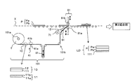
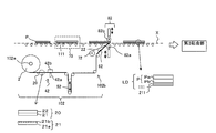
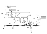
- FIG. 1 and FIGS. 2A to 2C are schematic views of a continuous manufacturing system of an optical display panel using the optical film roll set manufactured as described above.
- the continuous manufacturing system of the optical display panel according to the present embodiment will be specifically described with reference to FIG. 1 and FIGS. 2A to 2C.
- a horizontally long liquid crystal cell is used as an optical cell
- a horizontally long liquid crystal display panel is used as an example of an optical display panel.
- the optical film roll those shown in FIGS. 1 and 2A to 2C are used. That is, as the first optical film roll 1, a strip-shaped first polarizing film 11 (corresponding to the first optical film) having an absorption axis in the longitudinal direction is laminated on the first carrier film 12, and the liquid crystal cell P The belt-shaped first laminated optical film 10 having a width corresponding to the long side is wound.
- a strip-like linearly polarized light separating film 21 (corresponding to the second optical film) having a reflection axis in the width direction is laminated on the second carrier film 22.
- a film in which a belt-like second laminated optical film 20 having a width corresponding to the side is wound is used.
- a strip-shaped second polarizing film 31 (corresponding to the third optical film) having an absorption axis in the longitudinal direction is laminated on the third carrier film 32, and the liquid crystal cell P A belt-shaped third laminated optical film 30 having a width corresponding to the short side is wound.
- belt-shaped 1st polarizing film 11 has a strip
- the strip-shaped linearly polarized light separating film 21 is configured to include a strip-shaped film main body 21a and an adhesive 21b.
- the strip-shaped second polarizing film 31 includes a strip-shaped film body 31a and an adhesive 31b.
- the continuous manufacturing system 100 for a liquid crystal display panel includes a series of transport units X that transport the liquid crystal cells P and the liquid crystal display panel LD, a first optical film supply unit 101, The 1st bonding part 81, the 2nd optical film supply part 102, the 2nd bonding part 82, the 3rd optical film supply part 103, and the 3rd bonding part 83 are included.
- the transport unit X transports the liquid crystal cell P and the liquid crystal display panel LD.
- the conveyance unit X includes a plurality of conveyance rollers X1, a suction plate, and the like. Although details will be described later, in the present embodiment, the transport unit X is a length of the liquid crystal cell P between the first bonding unit 81 and the second bonding unit 82 with respect to the transport direction of the liquid crystal cell P.
- An arrangement replacement unit 75 for exchanging the arrangement relationship between the sides and the short sides is included.
- the first optical film supply unit 101 feeds a strip-shaped first laminated optical film 10 having a width corresponding to the long side of the liquid crystal cell P from the first optical film roll 1, and removes the strip-shaped first polarizing film 11 from the liquid crystal cell P.
- disconnecting in the width direction with the length corresponding to short side of this is supplied to the 1st bonding part 81.
- the first optical film supply unit 101 includes a first feeding unit 101a, a first cutting unit 41, a first tension adjusting unit 51, a first peeling unit 61, a first winding unit 71, and a plurality of conveying units. It has a roller part.
- the first feeding unit 101 a has a feeding shaft on which the first optical film roll 1 is installed, and feeds the strip-shaped first laminated optical film 10 from the first optical film roll 1.
- the first feeding unit 101a may be provided with two feeding shafts. Thereby, it is possible to quickly join the roll 1 to the roll film installed on the other feeding shaft without replacing the roll 1 with a new roll.
- the first cutting part 41 includes a cutting unit 41a and a suction unit 41b, and half-cuts the strip-shaped first laminated optical film 10 in the width direction with a length corresponding to the short side of the liquid crystal cell P (first).
- the band-shaped first polarizing film 11 is cut in the width direction without cutting the carrier film 12).
- the first cutting unit 41 uses the cutting unit 41a to fix the band-shaped first laminated optical film 10 from the first carrier film 12 side by using the suction unit 41b, and fixes the band-shaped first polarized light.
- the film 11 (the film body 11 a and the adhesive 11 b) is cut in the width direction, and the first polarizing film 111 having a size corresponding to the liquid crystal cell P is formed on the first carrier film 12.
- the cutting means 41a includes a cutter, a laser device, a combination thereof, and the like.
- the first tension adjusting unit 51 has a function of maintaining the tension of the belt-like first laminated optical film 10.
- the first tension adjusting unit 51 is configured to include a dancer roll, but is not limited thereto.
- the first peeling unit 61 peels the first polarizing film 111 from the first carrier film 12 by folding the first laminated optical film 10 having the first carrier film 12 on the inside.
- Examples of the first peeling portion 61 include a wedge-shaped member and a roller.
- the first winding unit 71 winds up the first carrier film 12 from which the first polarizing film 111 has been peeled off.
- the first winding unit 71 has a winding shaft on which a roll for winding the first carrier film 12 is installed.
- the 1st bonding part 81 was supplied by the 1st optical film supply part 101, conveying the liquid crystal cell P conveyed by the conveyance part X, making the short side direction parallel to a conveyance direction (1st peeling part).
- the first polarizing film 111 (removed by 61) from the long side of the liquid crystal cell P to the surface Pb on the back side of the liquid crystal cell P along the supply direction of the first polarizing film 111 (the short side direction of the liquid crystal cell P). It sticks together through the adhesive 11b.
- the first bonding unit 81 includes a pair of bonding rollers 81a and 81b, and at least one of the bonding rollers 81a and 81b includes a driving roller.
- the second optical film supply unit 102 feeds the strip-shaped second laminated optical film 20 having a width corresponding to the short side of the liquid crystal cell P from the second optical film roll 2, and the strip-shaped linearly polarized light separating film 21 is transferred to the liquid crystal cell P.
- the linearly polarized light separating film 211 obtained by cutting in the width direction with a length corresponding to the long side of the second side is supplied to the second bonding part 82.
- the second optical film supply unit 102 includes a second feeding unit 102a, a second cutting unit 42, a second tension adjusting unit 52, a second peeling unit 62, a second winding unit 72, and a plurality of conveyance units.
- the 2nd feeding part 102a, the 2nd cutting part 42, the 2nd tension adjustment part 52, the 2nd peeling part 62, and the 2nd winding part 72 are the 1st feeding part 101a, the 1st cutting part 41, and the 1st tension, respectively.
- the adjustment unit 51, the first peeling unit 61, and the first winding unit 71 have the same configuration and function.
- the 2nd bonding part 82 was supplied by the 2nd optical film supply part 102, conveying the liquid crystal cell P conveyed by the conveyance part X with the long side direction parallel to a conveyance direction (2nd peeling part).
- the linearly polarized light separating film 211 (removed by 62) from the short side of the liquid crystal cell P along the supply direction of the linearly polarized light separating film 211 (long side direction of the liquid crystal cell P) on the surface Pb on the back side of the liquid crystal cell P
- the first polarizing film 111 is bonded through an adhesive 21b.
- the 2nd bonding part 82 is comprised including a pair of bonding rollers 82a and 82b, and at least one of the bonding rollers 82a and 82b is configured by a drive roller.
- the third optical film supply unit 103 feeds the strip-shaped third laminated optical film 30 having a width corresponding to the short side of the liquid crystal cell P from the third optical film roll 3, and transfers the strip-shaped second polarizing film 31 to the liquid crystal cell P.
- disconnecting in the width direction with the length corresponding to the long side is supplied to the 3rd bonding part 83.
- FIG. In the present embodiment, the third optical film supply unit 103 includes a third feeding unit 103a, a third cutting unit 43, a third tension adjusting unit 53, a third peeling unit 63, a third winding unit 73, and a plurality of conveyance units. It has a roller part.
- the third feeding portion 103a, the third cutting portion 43, the third tension adjusting portion 53, the third peeling portion 63, and the third winding portion 73 are the first feeding portion 101a, the first cutting portion 41, and the first tension, respectively.
- the adjustment unit 51, the first peeling unit 61, and the first winding unit 71 have the same configuration and function.
- the 3rd bonding part 83 was supplied by the 3rd optical film supply part 103, conveying the liquid crystal cell P conveyed by the conveyance part X, making the long side direction parallel to a conveyance direction (3rd peeling part).
- the second polarizing film 311 (removed by 63) is applied to the surface Pa on the viewing side of the liquid crystal cell P along the supply direction of the second polarizing film 311 (long side direction of the liquid crystal cell P) from the short side of the liquid crystal cell P. It sticks together through the adhesive 31b.
- the 3rd bonding part 83 has a pair of bonding rollers 83a and 83b, and at least one of the bonding rollers 83a and 83b is comprised with a drive roller.
- the transport unit X includes a liquid crystal cell P in which the first polarizing film 111 is bonded between the first bonding unit 81 and the second bonding unit 82 in the transport direction of the liquid crystal cell P.
- An arrangement replacement unit 75 for exchanging the arrangement relationship between the long side and the short side is included.
- the arrangement replacement unit 75 adsorbs the liquid crystal cell P and rotates it 90 ° horizontally, and adsorbs the liquid crystal cell P, and is in a cell plane parallel or orthogonal to the transport direction of the liquid crystal cell P.
- a reversing unit that reverses the front and back of the liquid crystal cell P with the direction as a rotation axis.
- the bonding direction with respect to the liquid crystal cell P is relatively orthogonal to each other without orthogonally crossing the conveyance line of the strip-shaped first polarizing film 10 and the conveyance line of the strip-shaped linearly polarized light separating film 20. Therefore, the device space can be reduced.
- the first polarizing film and the linearly polarized light separating film which cannot be continuously laminated in the state of the belt-like film, are continuously supplied from the rolls, respectively.
- the supply direction is directly used as the bonding direction for the liquid crystal cell, and the bonding directions for the liquid crystal cell are relatively orthogonal to each other, whereby the liquid crystal cell can be continuously laminated at a high yield and at a high speed.
- the second polarizing film is also continuously supplied from the roll, and the supply direction from the roll is directly used as the bonding direction to the liquid crystal cell, so that the second polarizing film can be bonded to the surface on the viewing side of the liquid crystal cell at high speed and continuously. it can.
- the first polarizing film and the linearly polarized light separating film are laminated on the back side surface of the liquid crystal cell in an appropriate arrangement relationship, and the second polarizing film is crossed with the first polarizing film on the viewing side surface of the liquid crystal cell.
- a liquid crystal display panel with high light utilization efficiency bonded to have a Nicol relationship can be continuously produced at high yield and high speed.
- the first optical film supply unit, the second optical film supply unit, and the third optical film are arranged so that the supply directions of the first polarizing film, the linearly polarized light separating film, and the second polarizing film are parallel to each other. Since the supply unit is arranged, the space occupied by the apparatus can be reduced.
- a 1st bonding part, a 2nd bonding part, and a 3rd bonding part bond a 1st polarizing film and a linearly polarized light separation film from the lower side of a liquid crystal cell, and a 2nd polarizing film is a liquid crystal cell.
- the present invention is not limited to this. Any two sheets may be bonded from the upper side of the liquid crystal cell, and the remaining one may be bonded from the lower side of the liquid crystal cell, or all may be bonded from the upper side or the lower side of the liquid crystal cell.
- the 3rd optical film supply part supplies a 2nd polarizing film from a 3rd optical film roll like a 1st polarizing film and a linearly polarized light separation film,
- a 3rd optical film supply part may take out and supply a 2nd polarizing film from the container in which the 2nd polarizing film of the single wafer state was accommodated.
- the third optical film supply unit includes a moving unit that takes out the second laminated optical film from a container in which the second laminated optical film in a single wafer state is accommodated, and a second laminated optical material that is conveyed by the moving unit.
- the moving part may supply a second polarizing film having a peeling part that peels a single-wafer carrier film from the film, and the single-wafer carrier film is peeled off by the peeling part.
- a third optical film supply unit is suitable when the second polarizing film is not suitable for being bonded to a liquid crystal cell by the RTP method, or is a polarizing film that cannot be bonded.
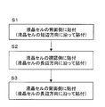
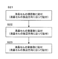
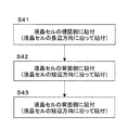
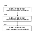
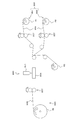
- 3A to 3F show examples of the order of the first, second, and third bonding steps, and the optical film bonding direction in each bonding step. Note that this embodiment is not limited to the order of FIGS. 3A to 3F, the attaching direction, and the type of optical film.
- the MD polarizing film is attached to the back side of the liquid crystal cell along the short side direction of the liquid crystal cell (that is, from the short side of the liquid crystal cell) (step S1), and then the MD polarizing film is attached to the liquid crystal cell.
- step S1 Affixed to the viewing side along the long side direction of the liquid crystal cell (that is, from the short side of the liquid crystal cell) (step S2), and then a linearly polarized light separating film (reflective polarizing film) is MD polarized on the back side of the liquid crystal cell.
- the film is pasted on the film along the long side direction of the liquid crystal cell (that is, from the short side of the liquid crystal cell) (step S3).
- the MD polarizing film is attached to the back side of the liquid crystal cell along the short side direction of the liquid crystal cell (step S11), and then the linearly polarized light separating film (reflective polarizing film) is MD on the back side of the liquid crystal cell.
- the polarizing film it is pasted along the long side direction of the liquid crystal cell (step S12), and then the MD polarizing film is pasted on the viewing side of the liquid crystal cell along the long side direction of the liquid crystal cell (step S13).
- the MD polarizing film is attached to the viewing side of the liquid crystal cell along the long side direction of the liquid crystal cell (step S21), and then the MD polarizing film is attached to the back side of the liquid crystal cell and the short side direction of the liquid crystal cell. (Step S22), and then a linearly polarized light separating film (reflective polarizing film) is pasted on the MD polarizing film on the back side of the liquid crystal cell along the long side direction of the liquid crystal cell (Step S23). .
- the retardation film is pasted on the back side of the liquid crystal cell along the short side direction of the liquid crystal cell (step S31), and then the MD polarizing film is placed on the viewing side of the liquid crystal cell and the long side direction of the liquid crystal cell. (Step S32), and then, the MD polarizing film is pasted on the retardation film on the back side of the liquid crystal cell along the short side direction of the liquid crystal cell (step S33).
- the MD polarizing film is attached to the viewing side of the liquid crystal cell along the long side direction of the liquid crystal cell (step S41), and then the retardation film is attached to the back side of the liquid crystal cell and the short side direction of the liquid crystal cell. (Step S42), and then, the MD polarizing film is pasted on the retardation film on the back side of the liquid crystal cell along the short side direction of the liquid crystal cell (Step S43).
- the retardation film is attached to the back side of the liquid crystal cell along the short side direction of the liquid crystal cell (step S51), and then the MD polarizing film is placed on the retardation film on the back side of the liquid crystal cell. Adhering along the short side direction of the liquid crystal cell (step S52), then, the MD polarizing film is applied to the viewing side of the liquid crystal cell along the long side direction of the liquid crystal cell (step S53).
- the absorption axes of the polarizing films on the viewing side and the back side of the liquid crystal cell are orthogonal (crossed Nicols), and the MD polarizing film on the viewing side is pasted along the long side direction of the liquid crystal cell.
- the back side MD polarizing film may be attached along the long side direction of the liquid crystal cell.
- a TD polarizing film can also be used.
- the optical film roll set of Embodiment 2 is composed of a first optical film roll and a second optical film roll.
- the first optical film roll 4 includes a band-shaped ⁇ / 4 retardation film having a slow axis in the longitudinal direction on the first carrier film 412 and the longitudinal direction.
- a belt-like retardation film 411 (corresponding to the first optical film) in which a belt-like ⁇ / 2 retardation film having a slow axis in a direction forming an angle of 67.5 degrees is laminated in this order is laminated,
- a film in which a strip-shaped first laminated optical film 410 having a width corresponding to the long side of the organic EL cell EL is wound is used.
- a strip-shaped polarizing film 521 (corresponding to the second optical film) having an absorption axis in the longitudinal direction is laminated on the second carrier film 522, and the short side of the organic EL cell EL.
- the belt-shaped second laminated optical film 520 having a width corresponding to is wound.
- belt-shaped retardation film 411 is comprised including the strip
- the strip-shaped polarizing film 521 includes a strip-shaped film main body 521a and an adhesive 521b.
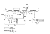
- FIGS. 5A to 5B are schematic views of a continuous production system for an organic EL display panel according to Embodiment 2.
- FIG. Hereinafter, the organic EL display panel continuous manufacturing system 400 according to this embodiment will be described in detail with reference to FIGS. 4 and 5A to 5B.
- a horizontally long organic EL cell is used as an optical cell
- a horizontally long organic EL display panel is used as an example of an optical display panel.
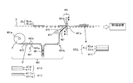
- the organic EL display panel continuous manufacturing system 400 includes a series of transport units X that transport the organic EL cells EL and the organic EL display panel OEL, and a first optical film supply unit 401. And the 1st bonding part 481, the 2nd optical film supply part 402, and the 2nd bonding part 482 are included.
- the transport unit X transports the organic EL cell EL and the organic EL display panel OEL.
- the conveyance unit X includes a plurality of conveyance rollers X1, a suction plate, and the like.
- the conveyance part X is the phase difference film 4111 with respect to the conveyance direction of the organic EL cell EL between the 1st bonding part 481 and the 2nd bonding part 482.
- the first optical film supply unit 401 feeds a strip-shaped first laminated optical film 410 having a width corresponding to the long side of the organic EL cell EL from the first optical film roll 4, and transfers the strip-shaped retardation film 411 to the organic EL cell.
- the retardation film 4111 obtained by cutting in the width direction with a length corresponding to the short side of the EL is supplied to the first bonding unit 81.
- the first optical film supply unit 401 includes a first feeding unit 401a, a first cutting unit 441, a first tension adjusting unit 451, a first peeling unit 461, a first winding unit 471, and a plurality of conveyances. It has a roller part.
- the first feeding unit 401 a has a feeding shaft on which the first optical film roll 4 is installed, and feeds the strip-shaped first laminated optical film 410 from the first optical film roll 4.
- the first feeding unit 401a may be provided with two feeding shafts. Thereby, it is possible to quickly join the roll 4 to the roll film installed on the other feeding shaft without replacing the roll 4 with a new roll.
- the first cutting part 441 includes a cutting unit 441a and a suction unit 441b, and half-cuts the strip-shaped first laminated optical film 410 in the width direction with a length corresponding to the short side of the organic EL cell EL (
- the belt-like retardation film 411 is cut in the width direction without cutting the first carrier film 412).
- the first cutting unit 441 uses the cutting unit 441a to adsorb and fix the band-shaped first laminated optical film 410 from the first carrier film 412 side using the adsorbing unit 441b.
- 411 film body 411a and adhesive 411b
- the cutting means 441a includes a cutter, a laser device, a combination thereof, and the like.
- the first tension adjusting unit 451 has a function of maintaining the tension of the band-shaped first laminated optical film 410.
- the first tension adjusting unit 451 is configured to include a dancer roll, but is not limited thereto.
- the first peeling portion 461 peels the retardation film 4111 from the first carrier film 412 by folding the strip-shaped first laminated optical film 410 with the first carrier film 412 inside.
- Examples of the first peeling portion 461 include a wedge-shaped member and a roller.
- the first winding unit 471 winds up the first carrier film 412 from which the retardation film 4111 has been peeled off.
- the first winding unit 471 includes a winding shaft on which a roll for winding the first carrier film 412 is installed.
- the 1st bonding part 481 was supplied by the 1st optical film supply part 401, conveying the organic EL cell EL conveyed by the conveyance part X, making the short side direction parallel to a conveyance direction (1st peeling).
- the surface of the retardation film 4111 (removed by the portion 461) from the long side of the organic EL cell EL along the supply direction of the retardation film 4111 (the short side direction of the organic EL cell EL) on the viewing side of the organic EL cell EL It is bonded to ELb via an adhesive 411b.
- the 1st bonding part 481 has a pair of bonding rollers 481a and 481b, and at least one of the bonding rollers 481a and 481b is comprised with a drive roller.
- the second optical film supply unit 402 feeds the strip-shaped second laminated optical film 520 having a width corresponding to the short side of the organic EL cell EL from the second optical film roll 5, and the strip-shaped polarizing film 521 is extracted from the organic EL cell EL.
- a polarizing film 5211 obtained by cutting in the width direction with a length corresponding to the long side of the sheet is supplied to the second bonding unit 482.
- the second optical film supply unit 402 includes a second feeding unit 402a, a second cutting unit 442, a second tension adjusting unit 452, a second peeling unit 462, a second winding unit 472, and a plurality of conveyance units. It has a roller part.
- the 2nd feeding part 402a, the 2nd cutting part 442, the 2nd tension adjustment part 452, the 2nd peeling part 462, and the 2nd winding part 472 are the 1st feeding part 401a, the 1st cutting part 441, and the 1st tension, respectively.
- the adjustment unit 451, the first peeling unit 461, and the first winding unit 471 have the same configuration and function.
- the 2nd bonding part 482 was supplied by the 2nd optical film supply part 402, conveying the organic EL cell EL conveyed by the conveyance part X, making the long side direction parallel to a conveyance direction (2nd peeling).
- the polarizing film 5211 (removed by the portion 462) on the surface ELb on the viewing side of the organic EL cell EL from the short side of the organic EL cell EL along the supply direction of the polarizing film 5211 (long side direction of the organic EL cell EL)
- the phase difference film 4111 is bonded through an adhesive 521b.
- the 2nd bonding part 482 has a pair of bonding rollers 482a and 482b, and at least one of the bonding rollers 482a and 482b is comprised with a drive roller.
- the transport unit X is an organic EL cell EL in which a retardation film 4111 is bonded between the first bonding unit 481 and the second bonding unit 482 in the transport direction of the organic EL cell EL.
- An arrangement replacement unit 475 that replaces the arrangement relationship between the long side and the short side is included.
- the arrangement replacement unit 475 has a rotating unit that sucks the organic EL cell EL and horizontally rotates it by 90 °.
- the bonding direction with respect to the organic EL cell EL is relatively orthogonal to each other without orthogonally crossing the conveyance line of the belt-like retardation film 411 and the conveyance line of the belt-like polarizing film 521. Therefore, the device space can be reduced.
- the retardation film and the polarizing film that cannot be continuously laminated in the state of the belt-like film are continuously supplied from each roll, and the supply direction from each roll Can be used as the bonding direction for the organic EL cell as it is, and the bonding direction for the organic EL cell are made to be relatively orthogonal to each other, so that the organic EL cell can be continuously laminated at a high yield and at a high speed.
- an organic EL display panel provided with an antireflection function by a circularly polarizing film in which a retardation film and a polarizing film are stacked in an appropriate arrangement relationship can be continuously produced at a high yield and at a high speed.
- the first optical film supply unit and the second optical film supply unit are arranged so that the supply directions of the retardation film and the polarizing film are parallel to each other, the space occupied by the apparatus is reduced. can do.
- the 1st bonding part and the 2nd bonding part bond the retardation film 4111 and the polarizing film 5211 from the lower side of an organic EL cell, it is not limited to this.
- any one sheet may be bonded together from the upper side of an organic EL cell, and the remaining one sheet may be bonded from the lower side of an organic EL cell, and both sheets are organic EL cells. You may stick together from above.
- the optical film roll set of Embodiment 3 includes a first optical film roll, a second optical film roll, and a fourth optical film roll. As shown in FIGS. 6 and 7A to 7C, as the first optical film roll 7, a band-like ⁇ / 4 retardation film 711 (first optical film) having a slow axis in the width direction on the first carrier film 712 is used. In which the belt-like first laminated optical film 710 having a width corresponding to the short side of the organic EL cell EL is wound is used.
- a band-shaped ⁇ / 2 retardation film 821 having a slow axis in a direction forming an angle of 67.5 degrees with respect to the longitudinal direction on the second carrier film 822 (second film) Used is one in which a belt-like second laminated optical film 820 having a width corresponding to the long side of the organic EL cell EL is wound.
- a strip-shaped polarizing film 931 (corresponding to the fourth optical film) having an absorption axis in the longitudinal direction is laminated on the fourth carrier film 932, and the organic EL cell EL is formed.
- a film in which a belt-like fourth laminated optical film 930 having a width corresponding to the short side is wound is used.
- the band-shaped ⁇ / 4 retardation film 711 includes a band-shaped film body 711a and an adhesive 711b as shown in FIG. 7A.
- the band-shaped ⁇ / 2 retardation film 821 is configured to include a band-shaped film main body 821a and an adhesive 821b.
- the strip-shaped polarizing film 931 includes a strip-shaped film main body 931a and an adhesive 931b.
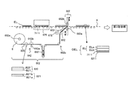
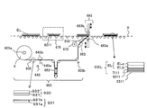
- FIGS. 7A to 7C are schematic views of a continuous production system for an organic EL display panel according to Embodiment 3.
- FIG. Hereinafter, the organic EL display panel continuous manufacturing system 600 according to the present embodiment will be described in detail with reference to FIG. 6 and FIGS. 7A to 7C.
- a horizontally long organic EL cell is used as an optical cell
- a horizontally long organic EL display panel is used as an example of an optical display panel.
- the organic EL display panel continuous manufacturing system 600 includes a series of transport units X that transport the organic EL cells EL and the organic EL display panel OEL, and a first optical film supply unit 601. And the 1st bonding part 681, the 2nd optical film supply part 602, the 2nd bonding part 682, the 4th optical film supply part 603, and the 4th bonding part 683 are included.
- the transport unit X transports the organic EL cell EL and the organic EL display panel OEL.
- the conveyance unit X includes a plurality of conveyance rollers X1, a suction plate, and the like.
- the conveyance part X is (lambda) / 4 rank with respect to the conveyance direction of the organic EL cell EL between the 1st bonding part 681 and the 2nd bonding part 682.
- positioning replacement part 675 which replaces the arrangement
- the conveyance part X is (lambda) / 2 phase difference film 7111 on it with respect to the conveyance direction of the organic EL cell EL between the 2nd bonding part 682 and the 4th bonding part 683.
- a second arrangement replacement unit 676 that exchanges the arrangement relationship between the short side and the long side of the organic EL cell EL to which the phase difference film 8211 is bonded is included.
- the first optical film supply unit 601 feeds a strip-shaped first laminated optical film 710 having a width corresponding to the short side of the organic EL cell EL from the first optical film roll 7, and strips the strip-shaped ⁇ / 4 retardation film 711.
- a ⁇ / 4 retardation film 7111 obtained by cutting in the width direction with a length corresponding to the long side of the organic EL cell EL is supplied to the first bonding unit 661.
- the first optical film supply unit 601 includes a first feeding unit 601a, a first cutting unit 641, a first tension adjusting unit 651, a first peeling unit 661, a first winding unit 671, and a plurality of conveying units. It has a roller part.
- the first feeding unit 601 a has a feeding shaft on which the first optical film roll 7 is installed, and feeds the belt-shaped first laminated optical film 710 from the first optical film roll 7.
- the first feeding unit 601a may be provided with two feeding shafts. Thereby, it is possible to quickly join the roll 7 to the roll film installed on the other feeding shaft without replacing the roll 7 with a new roll.
- the first cutting part 641 is configured to include cutting means 641a and suction means 641b, and half-cuts the strip-shaped first laminated optical film 710 in the width direction with a length corresponding to the long side of the organic EL cell EL ( The band-like ⁇ / 4 retardation film 711 is cut in the width direction without cutting the first carrier film 712).
- the first cutting unit 641 uses the cutting unit 641a to adsorb and fix the band-shaped first laminated optical film 710 from the first carrier film 712 side using the adsorbing unit 641b.
- the retardation film 711 (the film body 711a and the adhesive 711b) is cut in the width direction to form a ⁇ / 4 retardation film 7111 having a size corresponding to the organic EL cell EL on the first carrier film 712.
- the cutting means 641a include a cutter, a laser device, and a combination thereof.
- the first tension adjusting unit 651 has a function of maintaining the tension of the belt-shaped first laminated optical film 710.
- the first tension adjusting unit 651 is configured to have a dancer roll, but is not limited thereto.
- the first peeling portion 661 peels the ⁇ / 4 retardation film 7111 from the first carrier film 712 by folding the strip-shaped first laminated optical film 710 with the first carrier film 712 inside.
- Examples of the first peeling portion 661 include a wedge-shaped member and a roller.
- the first winding unit 671 winds up the first carrier film 712 from which the ⁇ / 4 retardation film 7111 is peeled off.
- the first winding unit 671 includes a winding shaft on which a roll for winding the first carrier film 712 is installed.
- the 1st bonding part 681 was supplied by the 1st optical film supply part 601, conveying the organic EL cell EL conveyed by the conveyance part X, making the long side direction parallel to a conveyance direction (1st peeling).
- the ⁇ / 4 retardation film 7111 (removed by the portion 661) from the short side of the organic EL cell EL along the supply direction of the ⁇ / 4 retardation film 7111 (long side direction of the organic EL cell EL). It is bonded to the surface ELb on the EL viewing side via an adhesive 711b.
- the 1st bonding part 681 has a pair of bonding rollers 681a and 681b, and at least one of the bonding rollers 681a and 681b is comprised with a drive roller.
- the second optical film supply unit 602 feeds a band-shaped second laminated optical film 820 having a width corresponding to the long side of the organic EL cell EL from the second optical film roll 8, and forms a band-shaped ⁇ / 2 retardation film 821 a.
- a ⁇ / 2 retardation film 8211 obtained by cutting in the width direction with a length corresponding to the short side of the organic EL cell EL is supplied to the second bonding unit 682.
- the second optical film supply unit 602 includes a second feeding unit 602a, a second cutting unit 642, a second tension adjusting unit 652, a second peeling unit 662, a second winding unit 672, and a plurality of conveyance units.
- the 2nd feeding part 602a, the 2nd cutting part 642, the 2nd tension adjustment part 652, the 2nd peeling part 662, and the 2nd winding part 672 are the 1st feeding part 601a, the 1st cutting part 641, and the 1st tension, respectively.
- the adjustment unit 651, the first peeling unit 661, and the first winding unit 671 have the same configuration and function.
- the 2nd bonding part 682 was supplied by the 2nd optical film supply part 602, conveying the organic EL cell EL conveyed by the conveyance part X, making the short side direction parallel to a conveyance direction (2nd peeling).
- ⁇ / 2 retardation film 8211 peeled by the portion 662 from the long side of the organic EL cell EL along the supply direction of the ⁇ / 2 retardation film 8211 (short side direction of the organic EL cell EL). It is bonded to the ⁇ / 4 retardation film 7111 on the EL viewing side ELb via an adhesive 821b.
- the 2nd bonding part 682 is comprised including a pair of bonding rollers 682a and 682b, and at least one of the bonding rollers 682a and 682b is configured by a drive roller.
- the transport unit X is an organic material in which a ⁇ / 4 retardation film 711 a is bonded between the first bonding unit 681 and the second bonding unit 682 in the transport direction of the organic EL cell EL.
- a first arrangement replacement unit 675 that exchanges the arrangement relationship between the short side and the long side of the EL cell EL is included.
- positioning replacement part 675 has a rotation part which adsorb
- the bonding direction with respect to organic EL cell EL is made without making the conveyance line of a strip
- the fourth optical film supply unit 603 feeds a strip-shaped fourth laminated optical film 920 having a width corresponding to the short side of the organic EL cell EL from the fourth optical film roll 9, and transfers the strip-shaped polarizing film 931 a to the organic EL cell EL.
- the polarizing film 9311 obtained by cutting in the width direction with a length corresponding to the long side of the film is continuously supplied to the fourth bonding unit 683.
- the fourth optical film supply unit 603 includes a fourth feeding unit 603a, a fourth cutting unit 643, a fourth tension adjusting unit 653, a third peeling unit 663, a fourth winding unit 673, and a plurality of conveying units. It has a roller part.
- the fourth feeding portion 603a, the fourth cutting portion 643, the fourth tension adjusting portion 653, the fourth peeling portion 663, and the fourth winding portion 673 are the first feeding portion 601a, the first cutting portion 641, and the first tension, respectively.
- the adjustment unit 651, the first peeling unit 661, and the first winding unit 671 have the same configuration and function.
- the 4th bonding part 683 was supplied by the 4th optical film supply part 603, conveying the organic EL cell EL conveyed by the conveyance part X, making the long side direction parallel to a conveyance direction (4th peeling). On the surface ELb on the back side of the organic EL cell EL from the short side of the organic EL cell EL along the supply direction of the polarizing film 9311 (long side direction of the organic EL cell EL). The ⁇ / 2 retardation film 8211 is bonded through an adhesive 931b.
- the 3rd bonding part 683 is comprised including a pair of bonding rollers 683a and 683b, and at least one of the bonding rollers 683a and 683b is configured by a drive roller.
- the transport unit X has a ⁇ / 4 retardation film 7111 and a ⁇ / 2 position between the second bonding unit 682 and the fourth bonding unit 683 with respect to the transport direction of the organic EL cell EL.
- a second arrangement replacement unit 676 that exchanges the arrangement relationship between the short side and the long side of the organic EL cell EL to which the phase difference film 8211 is bonded is included.
- the second arrangement replacement unit 676 includes a rotation unit that sucks the organic EL cell EL and horizontally rotates it by 90 °.
- the bonding direction with respect to the organic EL cell EL can be relatively relative to each other without causing the conveyance line of the band-like ⁇ / 2 retardation film and the conveyance line of the band-like polarizing film to be orthogonal to each other. Since they can be orthogonal, the apparatus space can be reduced.
- a ⁇ / 4 retardation film, a ⁇ / 2 retardation film, and a polarizing film which cannot be continuously laminated in the state of a belt-like film, are continuously formed from rolls.
- the direction of supply from each roll is directly used as the bonding direction for the organic EL cell, and the bonding direction for the organic EL cell is set as ⁇ / 4 retardation film, ⁇ / 2 retardation film, and ⁇ / 2 retardation.
- an organic EL display panel provided with an antireflection function by a circularly polarizing film in which a ⁇ / 4 retardation film, a ⁇ / 2 retardation film, and a polarizing film are stacked in an appropriate arrangement relationship can be obtained at high yield and high speed.
- the first optical film supply unit, the second optical film supply unit, and the fourth optical film supply unit are arranged so that the supply directions of the ⁇ / 4 retardation film, the ⁇ / 2 retardation film, and the polarizing film are parallel to each other. Since the optical film supply unit is disposed, the space occupied by the apparatus can be reduced.
- a 1st bonding part, a 2nd bonding part, and a 4th bonding part bond lambda / 4 phase difference film, (lambda) / 2 phase difference film, and a polarizing film from the lower side of an organic electroluminescent cell.
- Any two sheets may be bonded from the upper side of the organic EL cell, and the remaining one sheet may be bonded from the lower side of the organic EL cell. Any two sheets may be bonded from the lower side of the organic EL cell, and the remaining one sheet is bonded.
- the organic EL cell may be bonded from the upper side, or all may be bonded from the upper side of the organic EL cell.
- an optical film roll in which a belt-like laminated optical film formed by laminating a belt-like optical film on a carrier film is used, but the configuration of the optical film roll is not limited to this. .
- a belt-shaped laminated optical film formed by laminating a band-shaped optical film in which a plurality of score lines are formed in the width direction on a carrier film (a cut optical film roll).
- a cutting part becomes unnecessary in the optical film supply part which supplies an optical film from the optical film roll with a notch.
- each optical film supply unit half-cuts the band-shaped laminated optical film in the width direction (cuts the band-shaped optical film in the width direction without cutting the carrier film), and the optical film from the carrier film
- an optical film is supplied by peeling off, it is not limited to this structure.
- each optical film supply unit fully cuts a band-shaped laminated optical film in the width direction (cuts the carrier film and the band-shaped optical film in the width direction), and turns the sheet-shaped laminated optical film into a sheet-shaped carrier film.
- the optical film may be supplied by peeling the film.
- each optical film supply unit is particularly preferably configured as in the first to third embodiments.
- the cutting unit cuts the band-shaped optical film in the width direction to form an optical film having a size corresponding to the optical cell on the carrier film, but from the viewpoint of improving the yield. Cut the band-shaped optical film in the width direction (skip cut) so as to avoid the defective part of the band-shaped optical film, and the optical film of a size corresponding to the optical cell on the carrier film (good product to be bonded to the optical cell)
- the optical film including the defect portion may be formed with a size smaller than the optical cell (more preferably with a size as small as possible).
- the long optical films for example, a polarizing film
- the other optical film for example, a linearly polarized light separating film
- a first optical film for example, a polarizing film
- a second optical film for example, a linearly polarized light separating film
- each optical film supply unit is configured to supply the optical film obtained by skip-cutting the belt-shaped optical film in the width direction from the optical film roll.
- the first cutting part is configured to cut (skip cut) the band-shaped first optical film in the width direction so as to avoid the defective part of the band-shaped first optical film
- the second cutting part is formed of the band-shaped first optical film.
- the second optical film may be appropriately combined in such a manner that the second optical film is cut at a length corresponding to the optical cell in the width direction.
- a band-shaped optical film formed in the width direction so that a plurality of score lines avoid a defective portion is laminated on the carrier film, and corresponds to an optical cell on the carrier film.
- an optical film including a defective portion is formed in a size smaller than the optical cell (more preferably in a size as small as possible).
- the yield can be effectively improved by using a roll-shaped laminated optical film (an optical film roll having a cut).
- the optical film including the defective portion is peeled off from the carrier film and discharged, or wound around the winding portion together with the carrier film so as not to be bonded to the optical cell.
- the horizontally-long rectangular optical cell and the optical display panel have been described as examples.
- the shape of the optical cell and the optical display panel is another set of sides facing each other. As long as the shape has the following, there is no particular limitation.
Landscapes
- Physics & Mathematics (AREA)
- Nonlinear Science (AREA)
- General Physics & Mathematics (AREA)
- Optics & Photonics (AREA)
- Chemical & Material Sciences (AREA)
- Crystallography & Structural Chemistry (AREA)
- Engineering & Computer Science (AREA)
- Mathematical Physics (AREA)
- Forests & Forestry (AREA)
- Life Sciences & Earth Sciences (AREA)
- Mechanical Engineering (AREA)
- Manufacturing & Machinery (AREA)
- Polarising Elements (AREA)
- Liquid Crystal (AREA)
- Devices For Indicating Variable Information By Combining Individual Elements (AREA)
- Electroluminescent Light Sources (AREA)
Abstract
Description
前記光学セルの対向する一組の辺に対応する幅を有し、長手方向に吸収軸を有する帯状の偏光フィルムを含む帯状の第1積層光学フィルムが巻回されてなる第1光学フィルムロールと、
前記光学セルの対向するもう一組の辺に対応する幅を有し、幅方向に反射軸を有する帯状の直線偏光分離フィルムを含む帯状の第2積層光学フィルムが巻回されてなる第2光学フィルムロールと、を含む。
前記帯状の第2積層光学フィルムは、前記帯状の直線偏光分離フィルムに幅方向に複数の切込線が形成された状態で巻回されている。
長手方向に吸収軸を有する帯状の偏光フィルム原反を含む帯状の第1積層光学フィルム原反を、長手方向に平行に前記光学セルの対向する一組の辺に対応する幅でスリットし、得られた帯状の第1積層光学フィルムを巻回する工程と、
幅方向に反射軸を有する帯状の直線偏光分離フィルム原反を含む帯状の第2積層光学フィルム原反を、長手方向に平行に前記光学セルの対向するもう一組の辺に対応する幅でスリットし、得られた帯状の第2積層光学フィルムを巻回する工程と、を含む。
フィルムを供給し、当該フィルムの供給方向を光学セルに対する貼合方向とし、当該光学フィルムロールセットの光学フィルムロールを用いて各々フィルムが積層される光学セルの他方面に当該フィルムを積層するのに用いられる光学フィルムロールであって、前記光学セルの対向するもう一組の辺に対応する幅を有し、長手方向に吸収軸を有する帯状の偏光フィルムを含む帯状の第3積層光学フィルムが巻回されてなる第3光学フィルムロールと、を含む、少なくとも3個のロールを含む光学フィルムロールセットである。
前記光学セルの対向する一組の辺に対応する幅を有し、帯状の第1光学フィルムを含む帯状の第1積層光学フィルムが巻回されてなる第1光学フィルムロールと、
前記光学セルの対向するもう一組の辺に対応する幅を有し、帯状の第2光学フィルムを含む帯状の第2積層光学フィルムが巻回されてなる第2光学フィルムロールと、を含む。
帯状の第1光学フィルム原反を含む帯状の第1積層光学フィルム原反を、長手方向に平行に前記光学セルの対向する一組の辺に対応する幅でスリットし、得られた帯状の第1積層光学フィルムを巻回する工程と、
帯状の第2光学フィルム原反を含む帯状の第2積層光学フィルム原反を、長手方向に平行に前記光学セルの対向するもう一組の辺に対応する幅でスリットし、得られた帯状の第2積層光学フィルムを巻回する工程と、を含む。
帯状の第1光学フィルム原反を含む帯状の第1積層光学フィルム原反を、長手方向に平行に前記光学セルの対向する一組の辺に対応する幅でスリットし、得られた帯状の第1積層光学フィルムを巻回する工程と、
帯状の第2光学フィルム原反を含む帯状の第2積層光学フィルム原反を、長手方向に平行に前記光学セルの対向するもう一組の辺に対応する幅でスリットし、得られた帯状の第2積層光学フィルムを巻回する工程と、
帯状の第4光学フィルム原反を含む帯状の第4積層光学フィルム原反を、長手方向に平行に前記光学セルの対向するもう一組の辺に対応する幅でスリットし、得られた帯状の第4積層光学フィルムを巻回する工程と、
を含む。
前記帯状の第2光学フィルムが、長手方向に吸収軸を有する帯状の偏光フィルムである。
前記帯状の第2光学フィルムが、長手方向に対して67.5度の角度をなす方向に遅相軸を有する帯状のλ/2位相差フィルムであり、前記帯状の第4光学フィルムが、長手方向に吸収軸を有する帯状の偏光フィルムである。
帯状の第1光学フィルムを幅方向に切断することで得られた前記第1光学フィルムを第1光学フィルムロールから供給し、前記光学セルを搬送しながら、前記第1光学フィルムを前記光学セルの対向する一組の辺側から前記第1光学フィルムの供給方向に沿って前記光学セルの一方面に貼り合わせる第1貼合工程と、
帯状の第2光学フィルムを幅方向に切断することで得られた前記第2光学フィルムを第2光学フィルムロールから供給し、前記光学セルを搬送しながら、前記第2光学フィルムを前記光学セルの一方面に貼り合わされた前記第1光学フィルム上に、前記光学セルの対向するもう一組の辺側から前記第2光学フィルムの供給方向に沿って貼り合わせる第2貼合工程とを含む。
前記光学セルおよび前記光学表示パネルを搬送する一連の搬送部と、
帯状の第1光学フィルムを幅方向に切断することで得られた前記第1光学フィルムを第1光学フィルムロールから供給する第1光学フィルム供給部と、
前記搬送部によって搬送された前記光学セルを搬送しながら、前記第1光学フィルム供給部によって供給された前記第1光学フィルムを前記光学セルの対向する一組の辺側から前記第1光学フィルムの供給方向に沿って前記光学セルの一方面に貼り合わせる第1貼合部と、
帯状の第2光学フィルムを幅方向に切断することで得られた前記第2光学フィルムを第2光学フィルムロールから供給する第2光学フィルム供給部と、
前記搬送部によって搬送された前記光学セルを搬送しながら、前記第2光学フィルム供給部によって供給された前記第2光学フィルムを前記光学セルの一方面に貼り合わされた前記第1光学フィルム上に、前記光学セルの対向するもう一組の辺側から前記第2光学フィルムの供給方向に沿って貼り合わせる第2貼合部とを含む。
光学フィルムロールセットは、第1光学フィルムロールと、第2光学フィルムロールを少なくとも含む。
偏光フィルムのフィルム本体は、例えば、偏光子(厚さは一般的に1~80μm程度)と、偏光子の片面または両面に偏光子保護フィルム(厚さは一般的に1~500μm程度)が接着剤または接着剤なしで形成される。偏光子は、通常、延伸方向が吸収軸となっている。長手方向に吸収軸を有する長尺の偏光子を含む偏光フィルムを「MD偏光フィルム」ともいい、幅方向に吸収軸を有する長尺の偏光子を含む偏光フィルムものを「TD偏光フィルム」ともいう。フィルム本体を構成する他のフィルムとして、例えば、λ/4板、λ/2板等の位相差フィルム(厚さは一般的に10~200μm)、視角補償フィルム、輝度向上フィルム、表面保護フィルム等が挙げられる。積層光学フィルムの厚みは、例えば、10μm~500μmの範囲が挙げられる。
キャリアフィルムは、例えばプラスチックフィルム(例えば、ポリエチレンテレフタレート系フィルム、ポリオレフィン系フィルム等)等の従来公知のフィルムを用いることができる。また、必要に応じシリコーン系や長鎖アルキル系、フッ素系や硫化モリブデン等の適宜な剥離剤でコート処理したものなどの、従来に準じた適宜なものを用いうる。なお、キャリアフィルムは、一般的に離型フィルム(セパレータフィルム)ともいわれる。
液晶セルは、対向配置される一対の基板(第1基板(視認側面)Pa、第2基板(背面)Pb)間に液晶層が封止された構成である。液晶セルは、任意のタイプのものを用いることができるが、高コントラストを実現するためには、垂直配向(VA)モード、面内スイッチング(IPS)モードの液晶セルを用いることが好ましい。液晶表示パネルは、液晶セルの片面または両面に偏光フィルムが貼り合わされたものであり、必要に応じて駆動回路が組込まれる。
有機ELセルは、一対の電極間に電界発光層が挟持された構成である。有機ELセルは、例えば、トップエミッション方式、ボトムエミッション方式、ダブルエミッション方式などの任意のタイプのものを用いることができる。有機EL表示パネルは、有機ELセルの片面または両面に偏光フィルムが貼り合わされたものであり、必要に応じて駆動回路が組込まれる。
実施形態1の光学フィルムロールセットは、第1光学フィルムロール、第2光学フィルムロール、第3光学フィルムロールとで構成されている。第1光学フィルムロールおよび第2光学フィルムロールは、光学セルの一方面にフィルムを積層するのに用いられ、第3光学フィルムロールは、光学セルの他方面にフィルムを積層するのに用いられる。
光学フィルムロールセットを製造する方法は、長手方向に吸収軸を有する帯状の偏光フィルム原反を含む帯状の第1積層光学フィルム原反を、長手方向に平行に前記光学セルの対向する一組の辺に対応する幅でスリットし、得られた帯状の第1積層光学フィルムを巻回する工程と、幅方向に反射軸を有する帯状の直線偏光分離フィルム原反を含む帯状の第2積層光学フィルム原反を、長手方向に平行に前記光学セルの対向するもう一組の辺に対応する幅でスリットし、得られた帯状の第2積層光学フィルムを巻回する工程と、長手方向に吸収軸を有する帯状の偏光フィルム原反を含む帯状の第3積層光学フィルム原反を、長手方向に平行に前記光学セルの対向するもう一組の辺に対応する幅でスリットし、得られた帯状の第3積層光学フィルムを巻回する工程と、を含む。
図1及び図2A~2Cは、上記で製造された光学フィルムロールセットを用いた光学表示パネルの連続製造システムの概略図である。以下、図1及び図2A~2Cを参照しながら、本実施形態に係る光学表示パネルの連続製造システムを具体的に説明する。
搬送部Xは、液晶セルPおよび液晶表示パネルLDを搬送する。搬送部Xは、複数の搬送ローラX1および吸着プレート等を有して構成される。なお、詳細は後述するが、本実施形態では、搬送部Xは、第1貼合部81と第2貼合部82との間に、液晶セルPの搬送方向に対し、液晶セルPの長辺と短辺との配置関係を入れ替える配置入替部75を含む。
第1光学フィルム供給部101は、第1光学フィルムロール1から液晶セルPの長辺に対応する幅を有する帯状の第1積層光学フィルム10を繰り出し、帯状の第1偏光フィルム11を液晶セルPの短辺に対応する長さで幅方向に切断することで得られた第1偏光フィルム111を第1貼合部81に供給する。本実施形態では、第1光学フィルム供給部101は、第1繰出部101a、第1切断部41、第1張力調整部51、第1剥離部61、第1巻取部71、および複数の搬送ローラ部を有する。
第1貼合部81は、搬送部Xによって搬送された液晶セルPをその短辺方向を搬送方向に平行にして搬送しながら、第1光学フィルム供給部101によって供給された(第1剥離部61によって剥離された)第1偏光フィルム111を液晶セルPの長辺側から第1偏光フィルム111の供給方向(液晶セルPの短辺方向)に沿って液晶セルPの背面側の面Pbに粘着剤11bを介して貼り合わせる。なお、第1貼合部81は、一対の貼合ローラ81a、81bを有して構成され、貼合ローラ81a、81bの少なくとも一方が駆動ローラで構成される。
第2光学フィルム供給部102は、第2光学フィルムロール2から液晶セルPの短辺に対応する幅を有する帯状の第2積層光学フィルム20を繰り出し、帯状の直線偏光分離フィルム21を液晶セルPの長辺に対応する長さで幅方向に切断することで得られた直線偏光分離フィルム211を第2貼合部82に供給する。本実施形態では、第2光学フィルム供給部102は、第2繰出部102a、第2切断部42、第2張力調整部52、第2剥離部62、第2巻取部72、および複数の搬送ローラ部を有する。なお、第2繰出部102a、第2切断部42、第2張力調整部52、第2剥離部62、第2巻取部72はそれぞれ第1繰出部101a、第1切断部41、第1張力調整部51、第1剥離部61、第1巻取部71と同様の構成および機能を有する。
第2貼合部82は、搬送部Xによって搬送された液晶セルPをその長辺方向を搬送方向に平行にして搬送しながら、第2光学フィルム供給部102によって供給された(第2剥離部62によって剥離された)直線偏光分離フィルム211を液晶セルPの短辺側から直線偏光分離フィルム211の供給方向(液晶セルPの長辺方向)に沿って液晶セルPの背面側の面Pb上の第1偏光フィルム111に粘着剤21bを介して貼り合わせる。なお、第2貼合部82は、一対の貼合ローラ82a、82bを有して構成され、貼合ローラ82a、82bの少なくとも一方が駆動ローラで構成される。
第3光学フィルム供給部103は、第3光学フィルムロール3から液晶セルPの短辺に対応する幅を有する帯状の第3積層光学フィルム30を繰り出し、帯状の第2偏光フィルム31を液晶セルPの長辺に対応する長さで幅方向に切断することで得られた第2偏光フィルム311を第3貼合部83に供給する。本実施形態では、第3光学フィルム供給部103は、第3繰出部103a、第3切断部43、第3張力調整部53、第3剥離部63、第3巻取部73、および複数の搬送ローラ部を有する。なお、第3繰出部103a、第3切断部43、第3張力調整部53、第3剥離部63、第3巻取部73はそれぞれ第1繰出部101a、第1切断部41、第1張力調整部51、第1剥離部61、第1巻取部71と同様の構成および機能を有する。
第3貼合部83は、搬送部Xによって搬送された液晶セルPをその長辺方向を搬送方向に平行にして搬送しながら、第3光学フィルム供給部103によって供給された(第3剥離部63によって剥離された)第2偏光フィルム311を液晶セルPの短辺側から第2偏光フィルム311の供給方向(液晶セルPの長辺方向)に沿って液晶セルPの視認側の面Paに粘着剤31bを介して貼り合わせる。なお、第3貼合部83は、一対の貼合ローラ83a、83bを有して構成され、貼合ローラ83a、83bの少なくとも一方が駆動ローラで構成される。
本実施形態では、搬送部Xは、第1貼合部81と第2貼合部82との間に、液晶セルPの搬送方向に対し、第1偏光フィルム111が貼り合わされた液晶セルPの長辺と短辺との配置関係を入れ替える配置入替部75を含む。本実施形態では、配置入替部75は、液晶セルPを吸着して90°水平回転させる回転部と、液晶セルPを吸着し、液晶セルPの搬送方向に対して平行または直交するセル面内方向を回転軸にして液晶セルPの表裏を反転させる反転部とを有する。配置入替部75を含むことにより、帯状の第1偏光フィルム10の搬送ラインと帯状の直線偏光分離フィルム20の搬送ラインとを直交させることなく、液晶セルPに対する貼合方向を相対的に互いに直交させることができるため、装置スペースを削減することができる。
本実施形態では、第1貼合部、第2貼合部および第3貼合部は、搬送部Xによる液晶セルPの搬送方向に沿ってこの順に並んでいるが、第1貼合部、第2貼合部、第3貼合部の順序は、第1貼合部、第2貼合部がこの順に並んでいる限り、これに限定されない。例えば、搬送部Xによる液晶セルPの搬送方向に沿って、第1貼合部、第3貼合部、第2貼合部がこの順に並んでいてもよく、第3貼合部、第1貼合部、第2貼合部がこの順に並んでいてもよい。
実施形態2の光学フィルムロールセットは、第1光学フィルムロールと第2光学フィルムロールとで構成されている。図4、図5A~5Bに示すように、第1光学フィルムロール4としては、第1キャリアフィルム412上に長手方向に遅相軸を有する帯状のλ/4位相差フィルムと長手方向に対して67.5度の角度をなす方向に遅相軸を有する帯状のλ/2位相差フィルムとをこの順に積層した帯状の位相差フィルム411(第1光学フィルムに相当する)が積層されてなり、有機ELセルELの長辺に対応する幅を有する帯状の第1積層光学フィルム410が巻回されたものを用いる。第2光学フィルムロール5としては、第2キャリアフィルム522上に長手方向に吸収軸を有する帯状の偏光フィルム521(第2光学フィルムに相当する)が積層されてなり、有機ELセルELの短辺に対応する幅を有する帯状の第2積層光学フィルム520が巻回されたものを用いる。さらに、本実施形態では、帯状の位相差フィルム411は、図5Aに示すように、帯状のフィルム本体411aおよび粘着剤411bを有して構成される。帯状の偏光フィルム521は、図5Bに示すように、帯状のフィルム本体521aおよび粘着剤521bを有して構成される。
搬送部Xは、有機ELセルELおよび有機EL表示パネルOELを搬送する。搬送部Xは、複数の搬送ローラX1および吸着プレート等を有して構成される。なお、詳細は後述するが、本実施形態では、搬送部Xは、第1貼合部481と第2貼合部482との間に、有機ELセルELの搬送方向に対し、位相差フィルム4111が貼り合わされた有機ELセルELの長辺と短辺との配置関係を入れ替える配置入替部575を含む。
第1光学フィルム供給部401は、第1光学フィルムロール4から有機ELセルELの長辺に対応する幅を有する帯状の第1積層光学フィルム410を繰り出し、帯状の位相差フィルム411を有機ELセルELの短辺に対応する長さで幅方向に切断することで得られた位相差フィルム4111を第1貼合部81に供給する。本実施形態では、第1光学フィルム供給部401は、第1繰出部401a、第1切断部441、第1張力調整部451、第1剥離部461、第1巻取部471、および複数の搬送ローラ部を有する。
第1貼合部481は、搬送部Xによって搬送された有機ELセルELをその短辺方向を搬送方向に平行にして搬送しながら、第1光学フィルム供給部401によって供給された(第1剥離部461によって剥離された)位相差フィルム4111を有機ELセルELの長辺側から位相差フィルム4111の供給方向(有機ELセルELの短辺方向)に沿って有機ELセルELの視認側の面ELbに粘着剤411bを介して貼り合わせる。なお、第1貼合部481は、一対の貼合ローラ481a、481bを有して構成され、貼合ローラ481a、481bの少なくとも一方が駆動ローラで構成される。
第2光学フィルム供給部402は、第2光学フィルムロール5から有機ELセルELの短辺に対応する幅を有する帯状の第2積層光学フィルム520を繰り出し、帯状の偏光フィルム521を有機ELセルELの長辺に対応する長さで幅方向に切断することで得られた偏光フィルム5211を第2貼合部482に供給する。本実施形態では、第2光学フィルム供給部402は、第2繰出部402a、第2切断部442、第2張力調整部452、第2剥離部462、第2巻取部472、および複数の搬送ローラ部を有する。なお、第2繰出部402a、第2切断部442、第2張力調整部452、第2剥離部462、第2巻取部472はそれぞれ第1繰出部401a、第1切断部441、第1張力調整部451、第1剥離部461、第1巻取部471と同様の構成および機能を有する。
第2貼合部482は、搬送部Xによって搬送された有機ELセルELをその長辺方向を搬送方向に平行にして搬送しながら、第2光学フィルム供給部402によって供給された(第2剥離部462によって剥離された)偏光フィルム5211を有機ELセルELの短辺側から偏光フィルム5211の供給方向(有機ELセルELの長辺方向)に沿って有機ELセルELの視認側の面ELb上の位相差フィルム4111に粘着剤521bを介して貼り合わせる。なお、第2貼合部482は、一対の貼合ローラ482a、482bを有して構成され、貼合ローラ482a、482bの少なくとも一方が駆動ローラで構成される。
本実施形態では、搬送部Xは、第1貼合部481と第2貼合部482との間に、有機ELセルELの搬送方向に対し、位相差フィルム4111が貼り合わされた有機ELセルELの長辺と短辺との配置関係を入れ替える配置入替部475を含む。本実施形態では、配置入替部475は、有機ELセルELを吸着して90°水平回転させる回転部を有する。配置入替部475を含むことにより、帯状の位相差フィルム411の搬送ラインと帯状の偏光フィルム521の搬送ラインとを直交させることなく、有機ELセルELに対する貼合方向を相対的に互いに直交させることができるため、装置スペースを削減することができる。
本実施形態では、第1貼合部および第2貼合部は、位相差フィルム4111および偏光フィルム5211を有機ELセルの下側から貼り合わせるが、これに限定されない。第1貼合部および第2貼合部は、いずれか1枚を有機ELセルの上側から貼り合わせ、残り1枚を有機ELセルの下側から貼り合わせてもよく、2枚とも有機ELセルの上側から貼り合わせてもよい。
実施形態3の光学フィルムロールセットは、第1光学フィルムロールと第2光学フィルムロールと第4光学フィルムロールとで構成されている。図6、図7A~7Cに示すように、第1光学フィルムロール7としては、第1キャリアフィルム712上に幅方向に遅相軸を有する帯状のλ/4位相差フィルム711(第1光学フィルムに相当する)が積層されてなり、有機ELセルELの短辺に対応する幅を有する帯状の第1積層光学フィルム710が巻回されたものを用いる。また、第2光学フィルムロール8としては、第2キャリアフィルム822上に長手方向に対して67.5度の角度をなす方向に遅相軸を有する帯状のλ/2位相差フィルム821(第2光学フィルムに相当する)が積層されてなり、有機ELセルELの長辺に対応する幅を有する帯状の第2積層光学フィルム820が巻回されたものを用いる。さらに、第4光学フィルムロール9としては、第4キャリアフィルム932上に長手方向に吸収軸を有する帯状の偏光フィルム931(第4光学フィルムに相当する)が積層されてなり、有機ELセルELの短辺に対応する幅を有する帯状の第4積層光学フィルム930が巻回されたものを用いる。本実施形態では、帯状のλ/4位相差フィルム711は、図7Aに示すように、帯状のフィルム本体711aおよび粘着剤711bを有して構成される。帯状のλ/2位相差フィルム821は、図7Bに示すように、帯状のフィルム本体821aおよび粘着剤821bを有して構成される。帯状の偏光フィルム931は、図7Cに示すように、帯状のフィルム本体931aおよび粘着剤931bを有して構成される。
搬送部Xは、有機ELセルELおよび有機EL表示パネルOELを搬送する。搬送部Xは、複数の搬送ローラX1および吸着プレート等を有して構成される。なお、詳細は後述するが、本実施形態では、搬送部Xは、第1貼合部681と第2貼合部682との間に、有機ELセルELの搬送方向に対し、λ/4位相差フィルム7111が貼り合わされた有機ELセルELの短辺と長辺との配置関係を入れ替える第1配置入替部675を含む。また、搬送部Xは、第2貼合部682と第4貼合部683との間に、有機ELセルELの搬送方向に対し、λ/4位相差フィルム7111およびその上にλ/2位相差フィルム8211が貼り合わされた有機ELセルELの短辺と長辺との配置関係を入れ替える第2配置入替部676を含む。
第1光学フィルム供給部601は、第1光学フィルムロール7から有機ELセルELの短辺に対応する幅を有する帯状の第1積層光学フィルム710を繰り出し、帯状のλ/4位相差フィルム711を有機ELセルELの長辺に対応する長さで幅方向に切断することで得られたλ/4位相差フィルム7111を第1貼合部661に供給する。本実施形態では、第1光学フィルム供給部601は、第1繰出部601a、第1切断部641、第1張力調整部651、第1剥離部661、第1巻取部671、および複数の搬送ローラ部を有する。
第1貼合部681は、搬送部Xによって搬送された有機ELセルELをその長辺方向を搬送方向に平行にして搬送しながら、第1光学フィルム供給部601によって供給された(第1剥離部661によって剥離された)λ/4位相差フィルム7111を有機ELセルELの短辺側からλ/4位相差フィルム7111の供給方向(有機ELセルELの長辺方向)に沿って有機ELセルELの視認側の面ELbに粘着剤711bを介して貼り合わせる。なお、第1貼合部681は、一対の貼合ローラ681a、681bを有して構成され、貼合ローラ681a、681bの少なくとも一方が駆動ローラで構成される。
第2光学フィルム供給部602は、第2光学フィルムロール8から有機ELセルELの長辺に対応する幅を有する帯状の第2積層光学フィルム820を繰り出し、帯状のλ/2位相差フィルム821aを有機ELセルELの短辺に対応する長さで幅方向に切断することで得られたλ/2位相差フィルム8211を第2貼合部682に供給する。本実施形態では、第2光学フィルム供給部602は、第2繰出部602a、第2切断部642、第2張力調整部652、第2剥離部662、第2巻取部672、および複数の搬送ローラ部を有する。なお、第2繰出部602a、第2切断部642、第2張力調整部652、第2剥離部662、第2巻取部672はそれぞれ第1繰出部601a、第1切断部641、第1張力調整部651、第1剥離部661、第1巻取部671と同様の構成および機能を有する。
第2貼合部682は、搬送部Xによって搬送された有機ELセルELをその短辺方向を搬送方向に平行にして搬送しながら、第2光学フィルム供給部602によって供給された(第2剥離部662によって剥離された)λ/2位相差フィルム8211を有機ELセルELの長辺側からλ/2位相差フィルム8211の供給方向(有機ELセルELの短辺方向)に沿って有機ELセルELの視認側の面ELb上のλ/4位相差フィルム7111に粘着剤821bを介して貼り合わせる。なお、第2貼合部682は、一対の貼合ローラ682a、682bを有して構成され、貼合ローラ682a、682bの少なくとも一方が駆動ローラで構成される。
本実施形態では、搬送部Xは、第1貼合部681と第2貼合部682との間に、有機ELセルELの搬送方向に対し、λ/4位相差フィルム711aが貼り合わされた有機ELセルELの短辺と長辺との配置関係を入れ替える第1配置入替部675を含む。本実施形態では、第1配置入替部675は、有機ELセルELを吸着して90°水平回転させる回転部を有する。第1配置入替部675を含むことにより、帯状のλ/4位相差フィルムの搬送ラインと帯状のλ/2位相差フィルムの搬送ラインとを直交させることなく、有機ELセルELに対する貼合方向を相対的に互いに直交させることができるため、装置スペースを削減することができる。
第4光学フィルム供給部603は、第4光学フィルムロール9から有機ELセルELの短辺に対応する幅を有する帯状の第4積層光学フィルム920を繰り出し、帯状の偏光フィルム931aを有機ELセルELの長辺に対応する長さで幅方向に切断することで得られた偏光フィルム9311を第4貼合部683に連続的に供給する。本実施形態では、第4光学フィルム供給部603は、第4繰出部603a、第4切断部643、第4張力調整部653、第3剥離部663、第4巻取部673、および複数の搬送ローラ部を有する。なお、第4繰出部603a、第4切断部643、第4張力調整部653、第4剥離部663、第4巻取部673はそれぞれ第1繰出部601a、第1切断部641、第1張力調整部651、第1剥離部661、第1巻取部671と同様の構成および機能を有する。
第4貼合部683は、搬送部Xによって搬送された有機ELセルELをその長辺方向を搬送方向に平行にして搬送しながら、第4光学フィルム供給部603によって供給された(第4剥離部663によって剥離された)偏光フィルム9311を有機ELセルELの短辺側から偏光フィルム9311の供給方向(有機ELセルELの長辺方向)に沿って有機ELセルELの背面側の面ELb上のλ/2位相差フィルム8211に粘着剤931bを介して貼り合わせる。なお、第3貼合部683は、一対の貼合ローラ683a、683bを有して構成され、貼合ローラ683a、683bの少なくとも一方が駆動ローラで構成される。
本実施形態では、搬送部Xは、第2貼合部682と第4貼合部683との間に、有機ELセルELの搬送方向に対し、λ/4位相差フィルム7111およびλ/2位相差フィルム8211が貼り合わされた有機ELセルELの短辺と長辺との配置関係を入れ替える第2配置入替部676を含む。本実施形態では、第2配置入替部676は、有機ELセルELを吸着して90°水平回転させる回転部を有する。第2配置入替部676を含むことにより、帯状のλ/2位相差フィルムの搬送ラインと帯状の偏光フィルムの搬送ラインとを直交させることなく、有機ELセルELに対する貼合方向を相対的に互いに直交させることができるため、装置スペースを削減することができる。
本実施形態では、第1貼合部、第2貼合部および第4貼合部は、λ/4位相差フィルム、λ/2位相差フィルムおよび偏光フィルムを有機ELセルの下側から貼り合わせるが、これに限定されない。いずれか2枚を有機ELセルの上側から貼り合わせ、残り1枚を有機ELセルの下側から貼り合わせてもよく、いずれか2枚を有機ELセルの下側から貼り合わせ、残り1枚を有機ELセルの上側から貼り合わせてもよく、すべてを有機ELセルの上側から貼り合わせてもよい。
実施形態1~3では、光学フィルムロールとして、キャリアフィルム上に帯状の光学フィルムが積層されてなる帯状の積層光学フィルムが巻回されたものを用いるが、光学フィルムロールの構成はこれに限定されない。例えば、キャリアフィルム上に複数の切込線が幅方向に形成された帯状の光学フィルムが積層されてなる帯状の積層光学フィルムが巻回されたもの(切り目入りの光学フィルムロール)を適宜用いてもよい。なお、切り目入りの光学フィルムロールから光学フィルムを供給する光学フィルム供給部において、切断部は不要となる。
101、102、103、401、402、601、602、603 光学フィルム供給部
81、82、83、481、482、681、682、683 貼合部
P 液晶セル
LD 液晶表示パネル
EL 有機ELセル
OEL 有機EL表示パネル
X 搬送部
Claims (17)
- 各々フィルムを供給し、各々フィルムの供給方向を光学セルに対する貼合方向とし、前記光学セルに対する貼合方向を相対的に互いに直交させながら、前記光学セルの一方面に積層するのに用いられる光学フィルムロールセットであって、
前記光学セルの対向する一組の辺に対応する幅を有し、長手方向に吸収軸を有する帯状の偏光フィルムを含む帯状の第1積層光学フィルムが巻回されてなる第1光学フィルムロールと、
前記光学セルの対向するもう一組の辺に対応する幅を有し、幅方向に反射軸を有する帯状の直線偏光分離フィルムを含む帯状の第2積層光学フィルムが巻回されてなる第2光学フィルムロールと、を含む光学フィルムロールセット。 - 前記帯状の第1積層光学フィルムは、第1キャリアフィルム上に長手方向に吸収軸を有する帯状の偏光フィルムが積層された状態で巻回されており、および/または
前記帯状の第2積層光学フィルムが、第2キャリアフィルム上に幅方向に反射軸を有する帯状の直線偏光分離フィルムが積層された状態で巻回されている、請求項1に記載の光学フィルムロールセット。 - 前記帯状の第1積層光学フィルムは、前記帯状の偏光フィルムに幅方向に複数の切込線が形成された状態で巻回されており、および/または
前記帯状の第2積層光学フィルムは、前記帯状の直線偏光分離フィルムに幅方向に複数の切込線が形成された状態で巻回されている、請求項2に記載の光学フィルムロールセット。 - 前記光学セルが、VAモードまたはIPSモードの液晶セルである、請求項1から3のいずれかに記載の光学フィルムロールセット。
- 請求項1から4のいずれかに記載の光学フィルムロールセットを製造する方法であって、
長手方向に吸収軸を有する帯状の偏光フィルム原反を含む帯状の第1積層光学フィルム原反を、長手方向に平行に前記光学セルの対向する一組の辺に対応する幅でスリットし、得られた帯状の第1積層光学フィルムを巻回する工程と、
幅方向に反射軸を有する帯状の直線偏光分離フィルム原反を含む帯状の第2積層光学フィルム原反を、長手方向に平行に前記光学セルの対向するもう一組の辺に対応する幅でスリットし、得られた帯状の第2積層光学フィルムを巻回する工程と、
を含む光学フィルムロールセットの製造方法。 - 請求項1から4のいずれかに記載の光学フィルムロールセット、または請求項5に記載の製造方法で製造された光学フィルムロールセットと、
フィルムを供給し、当該フィルムの供給方向を光学セルに対する貼合方向とし、当該光学フィルムロールセットの光学フィルムロールを用いて各々フィルムが積層される光学セルの他方面に当該フィルムを積層するのに用いられる光学フィルムロールであって、前記光学セルの対向するもう一組の辺に対応する幅を有し、長手方向に吸収軸を有する帯状の偏光フィルムを含む帯状の第3積層光学フィルムが巻回されてなる第3光学フィルムロールと、を含む、少なくとも3個のロールを含む光学フィルムロールセット。 - 各々フィルムを供給し、光学セルに対する貼合方向を相対的に互いに直交させながら、前記光学セルの一方面に積層するのに用いられる光学フィルムロールセットであって、
前記光学セルの対向する一組の辺に対応する幅を有し、帯状の第1光学フィルムを含む帯状の第1積層光学フィルムが巻回されてなる第1光学フィルムロールと、
前記光学セルの対向するもう一組の辺に対応する幅を有し、帯状の第2光学フィルムを含む帯状の第2積層光学フィルムが巻回されてなる第2光学フィルムロールと、を含む光学フィルムロールセット。 - 前記帯状の第1光学フィルムと前記帯状の第2光学フィルムとは、光学的機能を共通にするフィルムを含まないことを特徴とする、請求項7に記載の光学フィルムロールセット。
- 前記帯状の第1積層光学フィルムは、第1キャリアフィルム上に前記帯状の第1光学フィルムが積層された状態で巻回されており、および/または
前記帯状の第2積層光学フィルムが、第2キャリアフィルム上に前記帯状の第2光学フィルムが積層された状態で巻回されている、請求項7または8に記載の光学フィルムロールセット。 - 前記帯状の第1積層光学フィルムは、前記帯状の偏光フィルムに幅方向に複数の切込線が形成された状態で巻回されており、および/または
前記帯状の第2積層光学フィルムは、前記帯状の第2光学フィルムに幅方向に複数の切込線が形成された状態で巻回されている、請求項9に記載の光学フィルムロールセット。 - フィルムを供給し、当該フィルムの供給方向を光学セルに対する貼合方向とし、前記光学セルの一方面に積層するのに用いられる光学フィルムロールであって、前記光学セルの対向する一組の辺に対応する幅を有し、帯状の第4光学フィルムを含む帯状の第4積層光学フィルムが巻回されてなる第4光学フィルムロールをさらに含む、請求項7から10のいずれかに記載の光学フィルムロールセット。
- 前記帯状の第1光学フィルムと前記帯状の第2光学フィルムと前記帯状の第4光学フィルムとは、光学的機能を共通にするフィルムを含まないことを特徴とする、請求項11に記載の光学フィルムロールセット。
- 前記帯状の第4積層光学フィルムは、第4キャリアフィルム上に前記帯状の第4光学フィルムが積層された状態で巻回されている、請求項11または12に記載の光学フィルムロールセット。
- 前記帯状の第4積層光学フィルムは、前記帯状の偏光フィルムに幅方向に複数の切込線が形成された状態で巻回されている、請求項13に記載の光学フィルムロールセット。
- 前記光学セルが、VAモードもしくはIPSモードの液晶セル、または有機ELセルである、請求項7から14のいずれかに記載の光学フィルムロールセット。
- 請求項7から15のいずれかに記載の光学フィルムロールセットを製造する方法であって、
帯状の第1光学フィルム原反を含む帯状の第1積層光学フィルム原反を、長手方向に平行に前記光学セルの対向する一組の辺に対応する幅でスリットし、得られた帯状の第1積層光学フィルムを巻回する工程と、
帯状の第2光学フィルム原反を含む帯状の第2積層光学フィルム原反を、長手方向に平行に前記光学セルの対向するもう一組の辺に対応する幅でスリットし、得られた帯状の第2積層光学フィルムを巻回する工程と、
を含む光学フィルムロールセットの製造方法。 - 請求項11から15のいずれかに記載の光学フィルムロールセットを製造する方法であって、
帯状の第1光学フィルム原反を含む帯状の第1積層光学フィルム原反を、長手方向に平行に前記光学セルの対向する一組の辺に対応する幅でスリットし、得られた帯状の第1積層光学フィルムを巻回する工程と、
帯状の第2光学フィルム原反を含む帯状の第2積層光学フィルム原反を、長手方向に平行に前記光学セルの対向するもう一組の辺に対応する幅でスリットし、得られた帯状の第2積層光学フィルムを巻回する工程と、
帯状の第4光学フィルム原反を含む帯状の第4積層光学フィルム原反を、長手方向に平行に前記光学セルの対向するもう一組の辺に対応する幅でスリットし、得られた帯状の第4積層光学フィルムを巻回する工程と、
を含む光学フィルムロールセットの製造方法。
Priority Applications (4)
| Application Number | Priority Date | Filing Date | Title |
|---|---|---|---|
| CN201280024442.9A CN103547962B (zh) | 2011-05-20 | 2012-05-09 | 光学薄膜卷组以及光学薄膜卷组的制造方法 |
| KR1020137022578A KR101552410B1 (ko) | 2011-05-20 | 2012-05-09 | 광학 필름 롤 세트 및 광학 필름 롤 세트의 제조 방법 |
| KR1020157016658A KR101799170B1 (ko) | 2011-05-20 | 2012-05-09 | 광학 필름 롤 세트 및 광학 필름 롤 세트의 제조 방법 |
| US14/118,013 US9261709B2 (en) | 2011-05-20 | 2012-05-09 | Optical film roll set, and method for producing optical film roll set |
Applications Claiming Priority (4)
| Application Number | Priority Date | Filing Date | Title |
|---|---|---|---|
| JP2011-113729 | 2011-05-20 | ||
| JP2011113729 | 2011-05-20 | ||
| JP2012-075232 | 2012-03-28 | ||
| JP2012075232A JP5945143B2 (ja) | 2011-05-20 | 2012-03-28 | 光学フィルムロールセットおよび光学フィルムロールセットの製造方法。 |
Publications (1)
| Publication Number | Publication Date |
|---|---|
| WO2012160966A1 true WO2012160966A1 (ja) | 2012-11-29 |
Family
ID=47217047
Family Applications (1)
| Application Number | Title | Priority Date | Filing Date |
|---|---|---|---|
| PCT/JP2012/061818 Ceased WO2012160966A1 (ja) | 2011-05-20 | 2012-05-09 | 光学フィルムロールセットおよび光学フィルムロールセットの製造方法 |
Country Status (6)
| Country | Link |
|---|---|
| US (1) | US9261709B2 (ja) |
| JP (1) | JP5945143B2 (ja) |
| KR (2) | KR101799170B1 (ja) |
| CN (1) | CN103547962B (ja) |
| TW (1) | TWI600948B (ja) |
| WO (1) | WO2012160966A1 (ja) |
Cited By (1)
| Publication number | Priority date | Publication date | Assignee | Title |
|---|---|---|---|---|
| CN107000325A (zh) * | 2015-02-19 | 2017-08-01 | 住友化学株式会社 | 层叠光学膜的制造方法以及液晶面板的制造方法 |
Families Citing this family (13)
| Publication number | Priority date | Publication date | Assignee | Title |
|---|---|---|---|---|
| JP5905761B2 (ja) | 2011-05-20 | 2016-04-20 | 日東電工株式会社 | 光学表示パネルの連続製造方法および光学表示パネルの連続製造システム |
| JP5931527B2 (ja) | 2011-05-20 | 2016-06-08 | 日東電工株式会社 | 液晶表示素子の製造方法および液晶表示素子の製造システム |
| JP6172980B2 (ja) | 2012-03-14 | 2017-08-02 | 日東電工株式会社 | 液晶表示パネルの製造方法 |
| US9211481B2 (en) * | 2012-07-27 | 2015-12-15 | Nb Tech Inc. | Visual display system and method of constructing a high-gain reflective beam-splitter |
| KR101932562B1 (ko) * | 2012-09-18 | 2018-12-28 | 삼성디스플레이 주식회사 | 필름 부착장치 및 그것을 이용한 필름 부착방법 |
| WO2014185099A1 (ja) * | 2013-05-17 | 2014-11-20 | 住友化学株式会社 | 光学表示デバイスの生産システム |
| KR101674252B1 (ko) * | 2014-04-21 | 2016-11-08 | 주식회사 엘지화학 | 광학 필름 라미네이팅 시스템 및 이를 이용한 디스플레이 유닛 제조방법 |
| JP6146921B2 (ja) * | 2014-12-02 | 2017-06-14 | 日東電工株式会社 | 光学フィルムの製造方法および製造装置 |
| KR101889144B1 (ko) * | 2015-04-30 | 2018-09-20 | 주식회사 엘지화학 | 디스플레이 유닛 제조방법 및 광학 필름 라미네이팅 시스템 |
| KR101674354B1 (ko) * | 2016-05-30 | 2016-11-22 | 주식회사 엘지화학 | 광학 표시 소자의 제조 시스템 및 제조 방법 |
| KR101674357B1 (ko) | 2016-07-08 | 2016-11-08 | 주식회사 엘지화학 | 디스플레이 유닛의 제조 시스템 및 제조 방법 |
| KR102042053B1 (ko) * | 2016-08-25 | 2019-11-07 | 주식회사 엘지화학 | 디스플레이 유닛의 제조 시스템 |
| JP6538014B2 (ja) * | 2016-09-06 | 2019-07-03 | 日東電工株式会社 | 光学的表示ユニットの連続製造装置及び連続製造方法 |
Citations (2)
| Publication number | Priority date | Publication date | Assignee | Title |
|---|---|---|---|---|
| JP2009271516A (ja) * | 2008-04-07 | 2009-11-19 | Nitto Denko Corp | 光学表示装置の製造方法 |
| JP2011081421A (ja) * | 2008-04-16 | 2011-04-21 | Nitto Denko Corp | 光学表示装置の製造方法、及びそれに用いるロール原反 |
Family Cites Families (39)
| Publication number | Priority date | Publication date | Assignee | Title |
|---|---|---|---|---|
| US6095220A (en) | 1997-06-23 | 2000-08-01 | Nisca Corporation | Overcoat fixing device |
| JP2002139625A (ja) | 2000-11-06 | 2002-05-17 | Nitto Denko Corp | 偏光部材、照明装置及び液晶表示装置 |
| JP2002189431A (ja) | 2000-12-21 | 2002-07-05 | Minolta Co Ltd | 積層型表示装置の製造方法 |
| JP2002196141A (ja) | 2000-12-26 | 2002-07-10 | Sumitomo Chem Co Ltd | 薄型光学フィルム積層体、その製造方法、及びそれの液晶表示素子への適用 |
| JP3870080B2 (ja) * | 2001-12-13 | 2007-01-17 | シャープ株式会社 | 液晶表示パネルの製造方法及び偏光フィルム貼付け装置 |
| JP2005037417A (ja) | 2002-06-28 | 2005-02-10 | Fuji Photo Film Co Ltd | 偏光板貼合方法及び装置 |
| KR20040002796A (ko) | 2002-06-28 | 2004-01-07 | 후지 샤신 필름 가부시기가이샤 | 편광판 점착방법 및 그 장치 |
| JP2004077768A (ja) | 2002-08-16 | 2004-03-11 | Fuji Photo Film Co Ltd | 偏光板及びその製造方法 |
| JP2004250213A (ja) | 2003-02-21 | 2004-09-09 | Sumitomo Chem Co Ltd | ロールフィルムの貼合せ方法 |
| JP4081389B2 (ja) | 2003-02-28 | 2008-04-23 | 住友化学株式会社 | シート貼合せ方法 |
| JP4371709B2 (ja) | 2003-06-05 | 2009-11-25 | 富士フイルム株式会社 | 光学フィルム貼付装置及び方法 |
| US7749348B2 (en) * | 2003-09-30 | 2010-07-06 | Nitto Denko Corporation | Method for manufacturing polarizing plate, polarizing plate, optical film and image viewing display |
| JP2005300877A (ja) | 2004-04-12 | 2005-10-27 | Dainippon Printing Co Ltd | 配向膜付シート、光学的異方性シート及び偏光板 |
| JP2005345958A (ja) | 2004-06-07 | 2005-12-15 | Nitto Denko Corp | 液晶パネル、偏光板および液晶表示装置 |
| JP3874200B2 (ja) * | 2004-11-22 | 2007-01-31 | 日東電工株式会社 | 光学補償層付偏光板、液晶パネル、液晶表示装置および光学補償層付偏光板の製造方法 |
| JP4714740B2 (ja) * | 2005-04-26 | 2011-06-29 | 帝人株式会社 | 偏光板 |
| JPWO2006118038A1 (ja) | 2005-04-28 | 2008-12-18 | コニカミノルタオプト株式会社 | 光学フィルム、偏光板及び横電界スイッチングモード型液晶表示装置 |
| JP4976075B2 (ja) | 2005-12-26 | 2012-07-18 | リンテック株式会社 | 偏光板用粘着剤、粘着剤付き偏光板及びその製造方法 |
| JP2008003188A (ja) * | 2006-06-21 | 2008-01-10 | Fujifilm Corp | 偏光板の製造方法,及び液晶表示装置 |
| JP5202889B2 (ja) | 2007-06-29 | 2013-06-05 | 日東電工株式会社 | 積層偏光板およびその製造方法ならびに液晶表示装置 |
| JP2009109602A (ja) | 2007-10-29 | 2009-05-21 | Hitachi Displays Ltd | 液晶表示装置 |
| JP2009157361A (ja) | 2007-12-06 | 2009-07-16 | Nitto Denko Corp | 偏光板及び画像表示装置 |
| JP5058953B2 (ja) | 2007-12-06 | 2012-10-24 | 日東電工株式会社 | 光学表示ユニットの製造方法およびそれに用いられるロール原反 |
| JP4307510B1 (ja) | 2007-12-27 | 2009-08-05 | 日東電工株式会社 | 光学表示装置の製造システム及び製造方法 |
| US8366858B2 (en) | 2007-12-27 | 2013-02-05 | Nitto Denko Corporation | Manufacturing system and manufacturing method for optical display device |
| JP4737569B2 (ja) | 2008-01-29 | 2011-08-03 | 日東電工株式会社 | 光学表示ユニットの製造方法および光学表示ユニットの製造システム |
| BRPI0822272A2 (pt) * | 2008-02-07 | 2015-06-23 | Sharp Kk | Método para produzir dispositivo de display de cristal líquido, e dispositivo de display de cristal líquido |
| US8087140B2 (en) | 2008-04-07 | 2012-01-03 | Nitto Denko Corporation | Optical member joining method and apparatus |
| JP4855493B2 (ja) * | 2008-04-14 | 2012-01-18 | 日東電工株式会社 | 光学表示装置製造システム及び光学表示装置製造方法 |
| JP4406043B2 (ja) | 2008-04-16 | 2010-01-27 | 日東電工株式会社 | ロール原反セット、及びロール原反の製造方法 |
| JP2009282385A (ja) | 2008-05-23 | 2009-12-03 | Nitto Denko Corp | 光学表示装置の製造方法 |
| JP4562795B2 (ja) | 2009-02-16 | 2010-10-13 | 日東電工株式会社 | ロール原反及びロール原反製造方法 |
| JP5407527B2 (ja) | 2009-04-28 | 2014-02-05 | 住友化学株式会社 | 光学表示パネルの製造方法 |
| JP4628488B1 (ja) | 2009-05-15 | 2011-02-09 | 日東電工株式会社 | 光学表示装置の製造システム及び製造方法 |
| EP2309313B1 (en) * | 2009-05-15 | 2013-03-27 | Nitto Denko Corporation | Optical display device manufacturing system and manufacturing method, and material roll set and method for manufacturing same |
| JP5792597B2 (ja) | 2010-11-25 | 2015-10-14 | 日東電工株式会社 | 液晶表示素子の製造方法および液晶表示素子の製造システム |
| JP5931527B2 (ja) | 2011-05-20 | 2016-06-08 | 日東電工株式会社 | 液晶表示素子の製造方法および液晶表示素子の製造システム |
| JP5905761B2 (ja) | 2011-05-20 | 2016-04-20 | 日東電工株式会社 | 光学表示パネルの連続製造方法および光学表示パネルの連続製造システム |
| JP5695981B2 (ja) | 2011-06-08 | 2015-04-08 | 日東電工株式会社 | 液晶表示素子の製造方法および液晶表示素子の製造システム |
-
2012
- 2012-03-28 JP JP2012075232A patent/JP5945143B2/ja not_active Expired - Fee Related
- 2012-05-09 KR KR1020157016658A patent/KR101799170B1/ko not_active Expired - Fee Related
- 2012-05-09 KR KR1020137022578A patent/KR101552410B1/ko not_active Expired - Fee Related
- 2012-05-09 WO PCT/JP2012/061818 patent/WO2012160966A1/ja not_active Ceased
- 2012-05-09 CN CN201280024442.9A patent/CN103547962B/zh not_active Expired - Fee Related
- 2012-05-09 US US14/118,013 patent/US9261709B2/en not_active Expired - Fee Related
- 2012-05-16 TW TW101117471A patent/TWI600948B/zh not_active IP Right Cessation
Patent Citations (2)
| Publication number | Priority date | Publication date | Assignee | Title |
|---|---|---|---|---|
| JP2009271516A (ja) * | 2008-04-07 | 2009-11-19 | Nitto Denko Corp | 光学表示装置の製造方法 |
| JP2011081421A (ja) * | 2008-04-16 | 2011-04-21 | Nitto Denko Corp | 光学表示装置の製造方法、及びそれに用いるロール原反 |
Cited By (2)
| Publication number | Priority date | Publication date | Assignee | Title |
|---|---|---|---|---|
| CN107000325A (zh) * | 2015-02-19 | 2017-08-01 | 住友化学株式会社 | 层叠光学膜的制造方法以及液晶面板的制造方法 |
| CN107000325B (zh) * | 2015-02-19 | 2018-06-15 | 住友化学株式会社 | 层叠光学膜的制造方法以及液晶面板的制造方法 |
Also Published As
| Publication number | Publication date |
|---|---|
| US9261709B2 (en) | 2016-02-16 |
| KR101799170B1 (ko) | 2017-11-17 |
| CN103547962B (zh) | 2016-04-27 |
| KR20150082648A (ko) | 2015-07-15 |
| TW201303441A (zh) | 2013-01-16 |
| CN103547962A (zh) | 2014-01-29 |
| JP2013008006A (ja) | 2013-01-10 |
| JP5945143B2 (ja) | 2016-07-05 |
| TWI600948B (zh) | 2017-10-01 |
| KR20130120528A (ko) | 2013-11-04 |
| US20140085723A1 (en) | 2014-03-27 |
| KR101552410B1 (ko) | 2015-09-10 |
Similar Documents
| Publication | Publication Date | Title |
|---|---|---|
| JP5945143B2 (ja) | 光学フィルムロールセットおよび光学フィルムロールセットの製造方法。 | |
| JP6126257B2 (ja) | 光学フィルムロールセットおよび光学フィルムロールセットの製造方法 | |
| JP5782010B2 (ja) | 光学表示パネルの連続製造方法および光学表示パネルの連続製造システム | |
| JP5905761B2 (ja) | 光学表示パネルの連続製造方法および光学表示パネルの連続製造システム | |
| JP5744819B2 (ja) | 光学表示パネルの連続製造方法および光学表示パネルの連続製造システム | |
| JP5933066B2 (ja) | 光学表示パネルの連続製造方法および光学表示パネルの連続製造システム | |
| JP6148755B2 (ja) | 光学表示パネルの連続製造方法および光学表示パネルの連続製造システム |
Legal Events
| Date | Code | Title | Description |
|---|---|---|---|
| WWE | Wipo information: entry into national phase |
Ref document number: 201280024442.9 Country of ref document: CN |
|
| 121 | Ep: the epo has been informed by wipo that ep was designated in this application |
Ref document number: 12789908 Country of ref document: EP Kind code of ref document: A1 |
|
| ENP | Entry into the national phase |
Ref document number: 20137022578 Country of ref document: KR Kind code of ref document: A |
|
| WWE | Wipo information: entry into national phase |
Ref document number: 14118013 Country of ref document: US |
|
| NENP | Non-entry into the national phase |
Ref country code: DE |
|
| 122 | Ep: pct application non-entry in european phase |
Ref document number: 12789908 Country of ref document: EP Kind code of ref document: A1 |