WO2012157719A1 - Optical filter and optical device - Google Patents
Optical filter and optical device Download PDFInfo
- Publication number
- WO2012157719A1 WO2012157719A1 PCT/JP2012/062700 JP2012062700W WO2012157719A1 WO 2012157719 A1 WO2012157719 A1 WO 2012157719A1 JP 2012062700 W JP2012062700 W JP 2012062700W WO 2012157719 A1 WO2012157719 A1 WO 2012157719A1
- Authority
- WO
- WIPO (PCT)
- Prior art keywords
- refractive index
- thin film
- substrate
- gradient
- film
- Prior art date
Links
Images


Classifications
-
- G—PHYSICS
- G02—OPTICS
- G02B—OPTICAL ELEMENTS, SYSTEMS OR APPARATUS
- G02B5/00—Optical elements other than lenses
- G02B5/20—Filters
- G02B5/22—Absorbing filters
-
- G—PHYSICS
- G02—OPTICS
- G02B—OPTICAL ELEMENTS, SYSTEMS OR APPARATUS
- G02B1/00—Optical elements characterised by the material of which they are made; Optical coatings for optical elements
- G02B1/10—Optical coatings produced by application to, or surface treatment of, optical elements
- G02B1/11—Anti-reflection coatings
- G02B1/113—Anti-reflection coatings using inorganic layer materials only
- G02B1/115—Multilayers
-
- G—PHYSICS
- G02—OPTICS
- G02B—OPTICAL ELEMENTS, SYSTEMS OR APPARATUS
- G02B1/00—Optical elements characterised by the material of which they are made; Optical coatings for optical elements
- G02B1/10—Optical coatings produced by application to, or surface treatment of, optical elements
- G02B1/11—Anti-reflection coatings
- G02B1/118—Anti-reflection coatings having sub-optical wavelength surface structures designed to provide an enhanced transmittance, e.g. moth-eye structures
-
- G—PHYSICS
- G02—OPTICS
- G02B—OPTICAL ELEMENTS, SYSTEMS OR APPARATUS
- G02B5/00—Optical elements other than lenses
- G02B5/20—Filters
- G02B5/205—Neutral density filters
-
- G—PHYSICS
- G02—OPTICS
- G02B—OPTICAL ELEMENTS, SYSTEMS OR APPARATUS
- G02B3/00—Simple or compound lenses
- G02B3/0087—Simple or compound lenses with index gradient
Definitions
- the present invention relates to an optical filter in which a light absorbing gradient refractive index thin film is provided on a light transmitting substrate, and an optical apparatus having an imaging optical system including the optical filter.
- optical filters used in a variety of different applications have problems due to their reflections.
- a phenomenon in which part of light transmitted through the filter is reflected by another member and is again incident on the optical filter from the light emission surface of the optical filter happens.
- the optical filter has a reflectance in the wavelength region of the incident light
- the light reflected by another member and incident is reflected again by the optical filter.
- a defect occurs due to the light reflected by the optical filter. Therefore, further enhancement of the anti-reflection function in the optical filter is strongly desired.
- an absorption-type ND (Neutral Density) filter used in a light quantity stop device etc. is generally widely known.
- the light amount stop is provided in an optical apparatus to control the amount of light incident on a solid-state image sensor such as a silver halide film or a CCD or CMOS sensor.
- Some light amount stops have a structure in which they are narrowed down as they become brighter in the field.
- the stop when photographing a clear field or a high-brightness object field, the stop is in a so-called small stop state, and is easily affected by the hunting phenomenon of the stop and the light diffraction phenomenon. It may cause deterioration in image performance.
- the ND filter is disposed in the vicinity of the diaphragm in the light path passing through the diaphragm, or the ND filter is attached directly to the diaphragm blade.
- a transparent substrate made of glass or a plastic material is used as a substrate constituting the ND filter.
- plastic materials for this substrate include PET (polyethylene terephthalate), PEN (polyethylene naphthalate), PC (polycarbonate) and PO (polyolefin).
- PET polyethylene terephthalate
- PEN polyethylene naphthalate
- PC polycarbonate
- PO polyolefin
- Arton made by JSR: product name
- Zeonex made by Nippon Zeon: product name
- Norbornene resins and polyimide resins are preferable.
- the light absorbing type ND filter includes a type in which an organic dye or pigment that absorbs light is mixed and kneaded into a substrate, and a type in which an organic dye or pigment that absorbs light is applied.
- an organic dye or pigment that absorbs light is mixed and kneaded into a substrate
- an organic dye or pigment that absorbs light is applied.
- Patent Document 1 Japanese Patent Application Laid-Open No. 8-075902
- Patent Document 2 several kinds of different refractive indexes made of different materials such as SiO 2 , MgF 2 , Nb 2 O 5 , TiO 2 , Ta 2 O 5 and ZrO 2 are used.
- a method has been proposed in which thin films are stacked to form a multilayer film type antireflective film, and the reflectance in an arbitrary wavelength range is suppressed.
- JP 2009-122216 A Patent Document 2 discloses an ND filter using a fine periodic structure as an anti-reflection structure.
- Patent Document 3 a method of improving the transmission flatness is proposed in Japanese Patent Laid-Open No. 2010-277094
- the fine periodic structure formed with sub-micron pitch shown in Patent Document 2 is used as an anti-reflection structure of an ND filter, the anti-reflection of the multi-layer film shown in Patent Document 1 is prevented. It is relatively easy to extend the wavelength range of (1), and it is also easy to reduce the reflectance. However, in the configuration in which the fine periodic structure is provided on the substrate described in Patent Document 2, light reflection at these interfaces may be a problem. Further, even in the case of a light absorption layer made of, for example, a multilayer thin film, it is extremely difficult to make all reflections of the ND filter as close to zero as possible by canceling all of the light reflections generated between the structures constituting the ND filter by the interference effect alone. It is.
- Patent Document 3 proposes a method of improving the flatness of transmittance by using an absorbing material having a small dispersion characteristic in a desired wavelength region. It is relatively easy to improve only the flatness of the transmittance and obtain the desired transmission characteristics. However, in order to significantly improve the flatness while reducing the reflectance to, for example, about 0.5% while maintaining a predetermined concentration, a very large number of layers is required, or an extremely thin layer is used. The problem arises that it becomes necessary and the design becomes very complicated.
- the optical filter according to the present invention comprises a light transmitting substrate, and a light absorbing refractive index gradient thin film which changes its refractive index so as to approach the substrate in the film thickness direction toward the substrate. It is characterized by
- An optical apparatus is characterized by having an imaging optical system provided with the above optical filter.
- an absorption type optical filter with reduced reflection can be obtained.
- this optical filter is used in a photographing optical system, it is possible to significantly reduce problems such as ghost caused by the reflection of the filter. Further, in the filter in which the flatness of the spectral transmission characteristic is improved, for example, the color balance and the like caused by the spectral transmission can be remarkably improved.
- an imaging apparatus using such an optical filter particularly for a light quantity stop apparatus can obtain an apparatus capable of achieving high image quality.
- FIG. 6 is a block diagram of an optical filter as Comparative Example 1; It is a spectral reflectance characteristic of ND filter produced by comparative example 1.
- FIG. FIG. 5 is a comparison diagram of spectral transmission characteristics of Example 1 and Example 2. It is the schematic of the fine periodic structure body of pillar array form. It is an example of arrangement of a fine periodic structure.
- FIG. 16 is a refractive index profile of a gradient refractive index thin film in Example 3.
- FIG. The substrate is disposed on the left side, and the anti-reflection structure is disposed on the right side. It is a spectral reflectance characteristic of the optical filter produced by Example 3.
- FIG. FIG. 7 is a block diagram of an optical filter manufactured according to Example 4. 21 is a configuration example of an optical filter described in Example 4.
- FIG. 7 is a refractive index profile of the gradient refractive index thin film described in Example 4.
- FIG. The substrate is disposed on the left side, and the anti-reflection structure is disposed on the right side. It is a spectral reflectance characteristic of the optical filter produced by Example 4.
- FIG. FIG. 18 is an explanatory view of a light amount stop apparatus using the ND filter of the fifth embodiment.
- FIG. 18 is an explanatory diagram of an optical system of an optical imaging apparatus using the ND filter of Example 5.
- FIG. 18 is an explanatory diagram of an optical measurement device using an ND filter according to a sixth embodiment.
- the optical filter according to the present invention includes a substrate having light transmittance, a gradient refractive index thin film having light absorbance, and preferably an antireflective structure.
- the substrate one having strength and optical characteristics as a substrate of an optical filter, which can function as a substrate for forming a gradient refractive index thin film and a reflection preventing structure, is used.
- a substrate made of a glass-based material PET (polyethylene terephthalate), PEN (polyethylene naphthalate), PES (polyether sulfone), PC (polycarbonate), PO (polyolefin), PI (polyimide) and PMMA (PM)
- PET polyethylene terephthalate
- PEN polyethylene naphthalate
- PES polyether sulfone
- PC polycarbonate
- PO polyolefin
- PI polyimide
- PM PMMA
- the refractive index gradient thin film changes the refractive index continuously or stepwise in the film thickness direction so as to approach the refractive index of the substrate, and the substrate and a structure adjacent to the atmosphere or the refractive index gradient thin film (for example, antireflective structure) And the difference in refractive index between
- the gradient refractive index thin film has a region in which the spectral transmission characteristic of the visible wavelength region increases as the long wavelength side increases, And a region where the spectral transmission characteristic of the light source decreases with increasing wavelength.
- the refractive index of the graded refractive index thin film continuously changes in the film thickness direction. By changing continuously, the effect of improving the antireflective effect and the environmental stability can be obtained. Also, if the structure adjacent to the graded refractive index thin film is an antireflective structure, the graded refractive index thin film reduces the difference in refractive index between the substrate and the antireflective structure.
- the refractive index difference between the substrate side end of the graded refractive index thin film and the refractive index difference between the side of the antireflective structure side of the graded refractive index thin film is set to be smaller than the refractive index difference between the substrate and the antireflective structure.
- the refractive index of the substrate and the refractive index of the antireflective structure are changed so as to continuously connect them.
- reflection on both sides of the substrate may be reduced by providing at least one of the antireflective structure and the gradient refractive index thin film on the opposite surface of the gradient refractive index thin film provided on one surface of the substrate.
- the graded refractive index thin film is a thin film having light absorption, and is disposed on the substrate in the thickness direction.
- an antireflective structure is provided on the gradient index thin film.
- the light absorptivity of the gradient index thin film is set in accordance with the function and characteristics of the target optical filter. When at least about 1% is absorbed with respect to a predetermined wavelength of incident light, it can be said to be light absorptive for the wavelength.
- the graded refractive index thin film has a change in refractive index that changes continuously and periodically in the thickness direction.
- the refractive index change of the graded refractive index thin film in the optical filter having the substrate, the graded refractive index thin film and the antireflective structure is (1) A portion on the substrate side where the refractive index changes so as to approach the refractive index of the substrate up to the end point on the substrate side of the refractive index change; (2) On the side of the antireflective structure, it is preferable to have a portion where the refractive index changes so as to approach the refractive index of the antireflective structure until the end point of the change of the refractive index on the side of the antireflective structure.
- the end point on the substrate side of the refractive index change is, for example, a point indicated by A in FIG. 1, and the end point on the fine periodic structure side for reflection prevention is indicated by B.
- the refractive index of the gradient refractive index thin film changes so as to approach the refractive index of the substrate at the end portion including the substrate side end point (or starting point) A of the change of the refractive index distribution.
- the refractive index of the gradient refractive index thin film changes similarly to the refractive index of the anti-reflection structure.
- the point A may be located at the substrate side interface.
- the point B may also be located at the interface on the side of the antireflective structure.
- the reflection can be greatly reduced, and the change in the refractive index is smooth and the refractive index of the adjacent structure, that is, the substrate or the fine periodic structure is larger. Even if it approaches, you may approach from the one where refractive index is smaller.
- the sum (a + b) with the refractive index difference b of the body may be smaller than the refractive index difference between the two structures adjacent to both sides of the gradient refractive index thin film.
- the refractive index of the substrate changes in the film thickness direction so as to reduce the difference in refractive index between the refractive index of the substrate and the refractive index of the material constituting the fine structure.
- of (a + b) between A and the refractive index B of the fine periodic structure is that
- this relationship is the same also in the case of the board
- the refractive index in the thickness direction is constant at the first portion of the thin film formed on the substrate.
- the compounding ratio of a plurality of thin film forming materials is changed to form a continuous change of the refractive index in the film thickness direction.
- the compounding ratio of a plurality of thin film forming materials can be changed after a certain time has elapsed since film formation was started at a constant film forming material concentration. In that case, there may be a portion where there is no change in the refractive index in the thickness direction as described above.
- the refractive index at the end point of the refractive index change on the substrate side is the same as the refractive index of the substrate, or within the range of the allowable refractive index difference in the characteristics of the target optical filter with respect to the refractive index of the substrate.
- the refractive index of Similarly, the refractive index at the end point of the refractive index change on the side of the antireflective structure is the same as the refractive index of the antireflective structure or, for the refractive index of the antireflective structure, the purpose in the wavelength or wavelength region of transmitted light
- the refractive index may be within the range of the refractive index difference permitted in the characteristics of the optical filter.
- the refractive index difference is preferably 0.05 or less.
- the refractive index of the portion without this change in refractive index is 0. 0 to the refractive index of the substrate. It is preferable to have a refractive index difference within 05. This point is the same as in the case where there is a portion in contact with the interface on the side of the anti-reflection structure and there is no change in refractive index in the thickness direction.
- the width of the change in refractive index in the thickness direction of the graded refractive index thin film can be set variously according to the characteristics of the target optical filter, the type of material for forming the graded refractive index thin film, and the combination thereof. For example, when changing from a region consisting of SiO 2 to a region consisting of TiO 2 using three kinds of elements in the thickness direction of the gradient refractive index thin film, change within the range of about 1.47 to 2.70 be able to.
- the film thickness of the refractive index gradient thin film can be appropriately selected according to the intended function.
- the film thickness of the refractive index gradient thin film can be 10 to 4000 nm, more preferably 100 to 1000 nm.
- the antireflective structure may be one having an antireflective function required to obtain the desired optical properties of the optical filter.
- an antireflective film formed of a fine structure or a thin film of a single layer or a plurality of layers can be used.
- a fine structure As a fine structure, a fine structure having a surface on which a large number of fine protrusions are arranged at a pitch shorter than the wavelength of visible light, or a surface provided with a repetition of unevenness at a pitch shorter than the wavelength of visible light
- the fine structure which it has can be used.
- the difference between the refractive index with the air or the adjacent medium is reduced by protrusions such as needles and pillars formed at random and protrusions or recesses of a concavo-convex structure finely formed in a step shape.
- protrusions such as needles and pillars formed at random and protrusions or recesses of a concavo-convex structure finely formed in a step shape.
- those selected from known microstructures in accordance with the purpose can be used.
- it has a periodic structure consisting of a large number of protrusions arranged at a repetition cycle shorter than the wavelength of visible light transmitted through the substrate, or a periodic structure consisting of an uneven structure with a repetition cycle shorter than the wavelength of visible light transmitted through the substrate If it is a fine periodic structure, it can be produced with good reproducibility using a method such as photo nanoimprinting.
- the refractive index gradient thin film has a refractive index in the film thickness direction so as to reduce the difference in refractive index between the refractive index of the layer adjacent to the refractive index gradient thin film and the refractive index of the substrate in a single layer or multiple layers of antireflective film Change.
- the substrate, the refractive index gradient thin film whose refractive index changes continuously in the film thickness direction, and the anti-reflection structure that exhibits the anti-reflection effect in the desired wavelength region of light are arranged adjacent to each other in this order.
- the light reflectance in the optical filter can be significantly reduced.
- the relationship between the refractive index of the substrate, the gradient refractive index thin film, and the anti-reflection structure is set as in (1) and (2) above using a thin film whose refractive index changes continuously and periodically. Is preferred. According to this preferred configuration, it is possible to obtain an absorption type optical filter in which the reflection is significantly reduced and the flatness of the spectral transmission characteristic is improved.
- the configuration of the optical filter according to the present invention can be used for various optical filters such as an ND filter, an optical filter, and the like, as long as it is an optical filter having absorption and an object of reflection.
- optical filter of the present invention will be described based on an embodiment in the case where it is used as an ND filter.
- the refractive index in the embodiment and each Example described below can be specified as a refractive index in the light of a wavelength of 540 nm from the constituent material of a board
- the gradient refractive index thin film 12 was disposed on one side (upper surface) of the substrate 13.
- the antireflective structure 111 is disposed on the gradient refractive index thin film 12 and the antireflective structure 112 is disposed on the back surface of the substrate 13, the antireflective effect can be further obtained.
- the gradient refractive index thin film 12 has absorption in at least a part of the film.
- such anti-reflection structures 111 and 112 include fine periodic structures 151 and 152 having an anti-reflection effect, and a single layer or a plurality of layers.
- the anti-reflective films 161 and 162 formed with the thin film are mentioned.
- FIGS. 3C to 3D a configuration in which the fine periodic structure 15 and the antireflective film 16 are used in combination may be mentioned.
- An optimal configuration may be selected appropriately. With such a configuration, for example, it is possible to suppress the generation of ghost light due to the reflection of the filter regardless of which side of the filter is directed to the imaging device side, and so on. It also becomes possible to arrange it.
- Example 3 of the present invention to be described later, as shown in FIG. 3A, fine periodic structures 151 and 152 are formed on the both sides of the substrate 13 as the anti-reflection structure.
- the refractive index is increased periodically and continuously a plurality of times in a predetermined region in the vicinity of the interface of the surface layer, and a refractive index profile for preventing interface reflection with external air is required. Therefore, it can be regarded as a configuration in which an antireflective structure is separately provided on the gradient refractive index thin film.
- the antireflective film use a material different from the material used to create the gradient index thin film on the gradient index thin film, and create an antireflection film in which the refractive index changes periodically and continuously. May be
- the gradient refractive index thin film 12 is desirably formed by mixing the two types while adjusting the film formation rate of the SiO 2 film and the TiO x film by the meta mode sputtering method and continuously changing the refractive index in the film thickness direction. Prepared to obtain the absorption characteristics of
- FIG. 1 and FIG. 1 An example of a graded refractive index thin film having such a continuous refractive index profile is shown in FIG. 1 and FIG.
- a substrate having a relatively high refractive index, a gradient refractive index thin film, and a fine periodic structure are stacked in this order. And, it has a change such that the refractive index continuously increases or decreases from the substrate side in the film thickness direction, and approaches the refractive index of the adjacent structure as it goes to the interface between both ends of the gradient index thin film I am changing.
- FIG. 1 shows the case where a substrate having a relatively high refractive index is laminated in the order of a refractive index gradient thin film and an antireflective structure such as a fine periodic structure. And, it has a change such that the refractive index continuously increases or decreases from the substrate side in the film thickness direction, and approaches the refractive index of the adjacent structure as it goes to the interface between both ends of the gradient index thin film I am changing.
- the substrate is on the left side of FIG. 1 as the structure, and the anti-reflection structure is on the right side.
- the refractive index is changed so as to approach the adjacent medium, for example, the atmosphere, water, an organic medium, and the like.
- the change in refractive index be gradual near the adjacent medium.
- the gradual change in the refractive index brings the compositions before and after the film thickness direction closer to each other, thereby further improving the environmental stability.
- the influence of the temporal change can be further reduced. Therefore, in the vicinity of A and B in FIG.
- the film thickness is larger than the refractive index change of the part C where the refractive index change causes the maximum refractive index change per film thickness which changes the refractive index between A and B continuously.
- the change in the refractive index per unit is slow, that is, a small change.
- the portion C where the maximum refractive index change per film thickness can be appropriately designed between A and B in consideration of absorption characteristics and the like.
- the graded refractive index thin film is a thin film in which the refractive index changes continuously, preferably continuously and periodically, in the direction perpendicular to the film surface, that is, in the film thickness direction.
- a film whose refractive index continuously and periodically changes in the film thickness direction can also be referred to as a rugate film, rugate filter, or the like.
- FIG. 5 shows a schematic view of an electron micrograph of the multilayer film and the refractive index gradient thin film.
- FIG. 5 (a) is a schematic view of a cross section in the film thickness direction of the multilayer film
- FIG. 5 (b) is a schematic view of a cross section of the refractive index gradient thin film.
- the interface of the film is clearly divided while the gradient index thin film is a multilayer film. Unlike, the interface of the membrane is not clearly divided. In addition, the contrast is enhanced in the portion where the refractive index change of the gradient refractive index thin film is large.
- a result obtained by the depth direction analysis is called a depth profile in which the concentration (intensity) is taken on the vertical axis and the depth (corresponding parameter such as film thickness) is taken on the horizontal axis.
- a method of analyzing while scraping the surface using accelerated ions is often used for analysis of micron order or less.
- This method is called ion sputtering, and is known as X-ray photoelectron spectroscopy (XPS), Auger electron spectroscopy (AES or ESCA), etc., and is an optical component or electron having a structure in which a layer is formed on the substrate surface. It is often used to evaluate parts and functional materials.
- a sample is irradiated with X-rays in ultra-high vacuum to detect emitted electrons (photoelectrons). Since the photoelectrons emitted are caused by the inner shell electrons of the target atom, and the energy is determined for each element, it is possible to conduct qualitative analysis by knowing the energy value. By evaluating the change in composition in the film thickness direction in the gradient refractive index thin film as described above and obtaining the depth profile, it is possible to confirm whether a desired refractive index distribution can be obtained.
- the range of the refractive index may be limited by the recent development of film forming methods such as sputtering and evaporation, an arbitrary refractive index can be obtained within at least the range.
- the discharge power of each material that is, the input power to the target is changed, and the mixing ratio is changed to have a refractive index between the two substances. It is possible to make an intermediate refractive index material. Moreover, two or more types may be mixed.
- the refractive index was changed within the range in which the discharge can be stably maintained and controlled. Moreover, in addition to changing the refractive index continuously in the film thickness direction, it is also possible to change x of TiOx in the film thickness direction and also change the extinction coefficient. As described above, in the configuration of the present embodiment, the refractive index and the extinction coefficient are changed by continuously changing the composition ratio of the three elements Ti, Si, and O in the film thickness direction of the gradient refractive index thin film. It can be changed continuously. Even when other substances are used or when the types of substances constituting the gradient refractive index thin film are increased, it is possible to similarly adjust. Also, the composition can be continuously changed by continuously changing the density of the thin film.
- the absorption characteristics in the gradient refractive index thin film 12 were adjusted by changing x of TiOx in the film thickness direction and changing the extinction coefficient. .
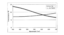
- the spectral transmission characteristics in the visible wavelength region of 400 nm to 700 nm were made to be flat characteristics with small dispersion as a whole film.
- the spectral transmission characteristics in the visible wavelength region tend to gradually increase as the long wavelength side increases, as shown in (a) in FIG.
- the spectral transmission characteristics in the visible wavelength region tend to gradually decrease toward the long wavelength side as shown in (b) in FIG. is there. Therefore, the spectral transmission characteristics are adjusted to be flat as a whole by providing one or more combinations in which the regions having mutually different dispersion shapes are arranged in the film thickness direction of the gradient refractive index thin film 12 as described above. The same tendency is shown when the ratio of metal to oxygen changes in metal oxides used for general optical thin films.
- the transmission is flat because the wavelength dependences of the transmittances of two or more types of metal oxides having different extinction coefficients, which are coefficients related to the transmittance, cancel each other's change.
- the idea of obtaining rate characteristics is disclosed in Japanese Patent No. 3359114.
- Film design can be performed to take advantage of this property of metal oxides to improve planarity.
- the refractive index is also changed by changing the value of x, it is necessary to determine and control the film forming ratio to SiO 2 from basic data obtained in advance based on this.
- the specific means for changing the value of x in the film thickness direction can be controlled by adjusting the power of the oxidation source or by adjusting the amount of introduced gas depending on the film forming method.
- FIG. 7 is a plan cross-sectional view in a plane orthogonal to the rotation axis of the substrate transfer device of the sputtering film forming apparatus used for producing the gradient refractive index thin film.
- a rotatable cylindrical substrate transfer device 52 for holding a substrate 51 on which a thin film is formed is provided in a vacuum chamber 53, and the outer periphery of the substrate transfer device 52 and the vacuum chamber 53 outside thereof.
- region 57 was used in the annular space between. Load the substrate from area 59.
- the substrate 51 was mounted on the substrate transfer device 52 so that the surface on which the film was formed was directed outward.
- the sputtered regions 54, 55 are equipped with AC double (dual) cathode type targets 54a, 55a.
- a high frequency power supply 56 is disposed outside the vacuum chamber 53.
- the shape of the target material is not limited to the flat plate type, and may be a cylindrical cylindrical type.
- an ion gun grid by high frequency excitation having a grid electrode, for example, separately in a region 58, and a neutralizer that emits low energy electrons for neutralizing positive ions to prevent charge accumulation of positive ions on the substrate. It is also possible to set etc.
- the sputtering apparatus used in the present invention may be provided with, for example, three or more sputtering areas, and configurations other than the above-described apparatus can be implemented.
- a Si target was disposed in the sputtering region 54 and a Ti target was disposed in the sputtering region 55, and oxygen was introduced into the reaction region 57 to form a graded refractive index thin film.
- the substrate 51 fixed to the substrate transfer device 52 is rotated at high speed to form an extremely thin film of Si and Ti on the substrate 51 in the sputtered regions 54 and 55, and then oxidized in the reaction region 57. . Thereby, an oxide film of Si and Ti was formed, and by repeating this operation, a mixed film of a Si oxide film and a Ti oxide film was produced.
- the discharge may become unstable if the input power is lowered, so the oxidation rate control
- the mask mechanism provided on the cathode was used together.
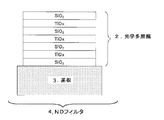
- Example 1 The absorption type ND filter configured as shown in FIG. 2 will be described in detail below.
- the gradient index thin film 12 having absorption in at least a part of the thin film is disposed on one side of the substrate 13.
- the anti-reflection structure was not provided.
- SFL-6 glass As a substrate 13 on which such an ND filter 14 is to be formed, SFL-6 glass having a thickness of 1.0 mm and a refractive index of 1.81 was used. In particular, a glass material was used to reduce the influence of water absorption of the substrate due to the single-sided film structure as in this example.
- the gradient refractive index thin film 12 was produced by mixing the two types while adjusting the film formation rate of the SiO 2 film and the TiO x film by the meta mode sputtering method. By continuously changing the composition in the film thickness direction, the refractive index was continuously changed in the film thickness direction, and adjustment was made to obtain desired absorption characteristics. Further, the film thickness of the gradient refractive index thin film 12 was adjusted to be 200 nm.
- the change in refractive index in the film thickness direction of the gradient refractive index thin film 12 is designed so as to be minimally increased / decreased so as not to be complicated.
- the refractive index profile is such that one peak is raised and lowered from the refractive index of the substrate 13.
- the maximum value of the refractive index change per film thickness is set, refraction is more complicated when the inflection point is one with a peak on the substrate 13 (high refractive index) side, having a plurality of peaks and valleys.
- the refractive index of the adjacent medium (including the substrate 13) of the rate gradient thin film 12 can be easily changed gradually.
- the substrate 13 is made of glass and has a refractive index higher than that of the air or general plastic. Therefore, the inflection point is refracted toward the substrate 13 in the graded refractive index thin film 12 to give predetermined absorption, that is, toward the substrate 13 side from the center position in the film thickness direction of the graded refractive index thin film. A pile was made to raise and lower the rate. In order to achieve a gradual change in refractive index toward the atmosphere side, through the portion that has the maximum change rate per film thickness in the film thickness direction in the graded refractive index thin film from the mountain to the point C in FIG. Configured.
- the end point of the gradient refractive index thin film 12 is configured to be a thin film of SiO 2 from the viewpoints of the reflection prevention and the environmental stability. Therefore, the refractive index at the end point of the graded refractive index thin film 12 is approximately 1.47.
- the spectral transmittance characteristic of the ND filter manufactured as described above is shown in FIG. This was put into a high temperature test under a dry nitrogen atmosphere, and the transmittance at a wavelength of 540 nm after 1000 hours was compared before and after the test. The transmittance was 17.2% to 17.4%, and the rate of increase was about 0.1%.
- a single density ND filter was created.
- a mask having a shield capable of adjusting the angle with the mask surface is used. Then, by shielding a part of the film material from the surface of the target with a mask, it can be formed by using a method of forming a gradation density distribution on the substrate.
- Example 1 In order to consider the effect of environmental stability in Example 1, a spectral transmittance characteristic substantially similar to that of FIG. 8 is produced with a film thickness of 200 nm using a multilayer film configuration, and other materials and processes are as much as possible.
- the ND filter 4 manufactured to be similar to that of the first embodiment will be described below.
- an optical multilayer film 2 was formed by alternately laminating seven layers of SiO 2 and TiO x on one side of the substrate 3.
- an ND filter 4 having spectral transmittance characteristics substantially similar to those of the ND filter 14 manufactured in Example 1 was manufactured.
- SFL-6 glass with a refractive index of 1.81 and a thickness of 1.0 mm was used as a substrate 3 on which such an ND filter 4 is formed.
- SiO 2 and TiO x were formed by meta mode sputtering.
- the ND filter fabricated in this manner was put into a high temperature test under a dry nitrogen atmosphere, and the increase in transmittance at a wavelength of 540 nm after 1000 hours was confirmed.
- the transmittance was 16.9 before and after the test. It became about 0.4% change from 1% to 17.6%.
- the results showed a very large change.
- Example 2 In the same manner as in Example 1, a 1.0 mm thick SFL-6 glass was used as the substrate 13, and an ND filter composed of the substrate 13 and the gradient refractive index thin film 12 was produced.
- the composition of the graded refractive index thin film 12 is continuously mixed by mixing these two types while adjusting the film forming rate of the SiO 2 and TiO x films by meta mode sputtering so that the film thickness becomes 200 nm.
- the refractive index was continuously changed in the film thickness direction, and was adjusted and manufactured so as to obtain a desired absorption characteristic.
- the refractive index gradient thin film 12 is a region in which the spectral transmittance in the visible wavelength region becomes higher as it goes to the long wavelength side and a region that becomes lower as it goes to the long wavelength side. It was set up in the inside. As described above, by providing regions having opposite dispersion shapes in the same film in the spectral transmittance in a specific wavelength region, for example, in the case of an ND filter, a flatter spectral transmission characteristic with smaller wavelength dispersion. It is possible to get.
- the refractive index profile of the gradient refractive index thin film 12 is designed to be minimally increased or decreased so as not to be complicated. It was set as the refractive index profile from which the peak made to raise and lower a refractive index from the refractive index of the board
- the composition ratio of the mixed film corresponding to SiO 2 and TiO was adjusted so that the gradient refractive index thin film 12 had a refractive index of 1.81 close to the substrate 13 at the interface with the substrate 13. Then, as the distance from the substrate 13 in the film thickness direction is increased, the composition ratio corresponding to TiO 2 to SiO 2 is gradually increased, and when the refractive index becomes 2.1, the composition ratio of these two materials is continuous.
- the composition ratio of SiO 2 to Ti 2 O 3 is gradually increased. It changed to the continuous change of the composition ratio of the material, and the end point of the gradient index thin film 12 was configured to be SiO 2 from the viewpoints of the reflection prevention and the environmental stability. Therefore, the refractive index at the end point of the graded refractive index thin film 12 is approximately 1.47.
- the refractive index gradient thin film includes the region showing the spectral transmission strongly influenced by TiO and the region showing the spectral transmission strongly influenced by Ti 2 O 3 .
- regions having different dispersion characteristics as illustrated in FIG. 6 in the visible wavelength region it is possible to obtain desired transmission characteristics.
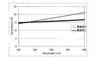
- the spectral transmittance characteristic of the ND filter manufactured as described above is shown in FIG. From FIG. 11, it can be confirmed that the flatness of the spectral transmittance in the visible wavelength region is improved as compared with the ND filter manufactured in Example 1.
- the fine periodic structure has come to be manufactured with the improvement of the micro processing technology in recent years.
- One of such structures a fine periodic structure having an antireflective effect, can also be generally called a moth-eye structure or the like.
- FIG. 12 is a top perspective view showing a schematic example of a fine periodic structure having an anti-reflection effect, in which cones are arranged in a pillar array on a substrate. Similarly to this, it is also possible to form fine periodic structures arranged in a hole array. Such a structure is often produced, for example, on the surface of a material or the like as a means other than an antireflective film produced by laminating a thin film in a single layer or a plurality of layers by vacuum deposition or the like.
- the fine periodic structure is in the form of a pillar array in which cones are periodically arranged as shown in FIG. 12, and considering the application of the ND filter, the structure has a height such that the reflectance in the visible wavelength region can be reduced at least. It was designed to be 350 nm and have a period of 250 nm. Furthermore, with regard to the matrix-like arrangement of the projection structures, a tetragonal arrangement can be considered as shown in the plan view of FIG. 13A, a three-way (hexagonal) arrangement etc. as shown in the plan view of FIG. The three-way arrangement is said to have a high anti-reflection effect because the exposed surface of the substrate material is smaller. Therefore, in this embodiment, a pillar array of three-way arrangement is used.
- UV curable resin An appropriate amount of a UV curable resin was dropped on a quartz substrate as a mold having a hole array shape whose shape is inverted previously designed. Thereafter, the resin is cured by irradiating the UV light in a state where the quartz mold is pressed against the substrate to be imprinted, and as shown in FIG. 3A, a submicron pitch pillar array-shaped fine periodic structure 151, 152 was produced.
- PAK-01 trade name
- Toyo Gosei Co., Ltd. was used to adjust the refractive index to be 1.50 after polymerization and curing.
- a primer treatment was performed to provide an adhesive layer between the gradient refractive index thin film and the fine periodic structure.
- IPA isopropyl alcohol
- nitric acid is added based on KBM-503 (trade name) manufactured by Shin-Etsu Chemical Co., Ltd., which is a surfactant, and the refractive index of the cured adhesion layer after coating is 1 The one adjusted to be .45 was used.
- the resultant was dropped onto a gradient refractive index thin film through a 0.2 ⁇ m PTFE (polytetrafluoroethylene) filter, and was coated by spin coating so as to be an extremely thin film. If it is necessary to further strengthen the adhesion, TEOS (tetraethyl orthosilicate) or the like may be further added to the components of the above-mentioned primer solution. Further, in order to apply the primer solution more uniformly, it is more preferable to subject the substrate to a hydrophilization treatment with UV ozone before the primer solution application.
- TEOS tetraethyl orthosilicate
- the concentration may be appropriately adjusted, and coating may be performed by dip coating, or after one side coating by spin coating, the front and back of the substrate is changed, and the other side is again coated by spin coating.
- the process may be performed, the latter is selected in this embodiment.
- the difference in refractive index between the adhesive layer and the adjacent structure is also preferably 0.05 or less.
- a filter having absorption in the entire visible wavelength range such as an ND filter
- a PET film having a thickness of 0.1 mm was used so that the refractive index was about 1.60.
- a PET film is used, but the material is not limited thereto, and a glass material may be used, or a resin material such as PO, PI, PEN, PES, PC, or PMMA may be used.
- x of TiOx is fixed at about 1.5 from the interface point P0 on the substrate side to the point P1, and it is continuous by changing the composition ratio to SiO 2 Form a refractive index change.
- x of TiOx is continuously changed from 1.5 to 1.0.
- the composition ratio to SiO 2 is changed, and the composition ratio of SiO 2 to TiOx is increased as it approaches point P 2 from point P 1, and the composition ratio of SiO 2 to TiO x as it further approaches point P 3 from point P 2
- a continuous change in refractive index By forming a continuous change in refractive index.
- x of TiO x is fixed at about 1.0, and a continuous change in refractive index is formed by changing the composition ratio with SiO 2 .
- the spectral transmission largely influenced by Ti 2 O 3 is shown, and in the vicinity of the point P3, the spectral transmission largely influenced by TiO is shown. Therefore, by configuring in this way, in the refractive index gradient thin film, regions having different dispersion characteristics as illustrated in FIG. 6 in the visible wavelength region are mixed, and the degree of influence is adjusted by the film thickness and composition ratio. Thus, it is possible to obtain desired transmission characteristics. In the present embodiment, these were adjusted so that the spectral transmission characteristics had a flat shape in the visible wavelength region.
- the gradient refractive index thin film 12 is configured to have a refractive index profile as shown in FIG.
- FIG. 14 (b) it is possible to form the profile shown in FIG. 14 (b) in which a plurality of peaks and valleys in FIG. 14 (a) are formed, it is necessary to prevent complication due to ease of control. It was designed to be an increase or decrease.
- a refractive index difference is likely to occur at the interface between the substrate and the antireflective structure. From the viewpoint of anti-reflection, in the area close to the substrate and the anti-reflection structure, the film was designed so that the change in refractive index was gradual.
- the refractive index gradient thin film gently increase the refractive index from the side close to the substrate, and gradually approach the refractive index of the antireflective structure toward the antireflective structure through an inflection point.
- the refractive index difference between the two interfaces is 0.05 or less respectively by adjusting the rate ratio between SiO 2 and TiO x immediately after the start of film formation and near the end of film formation of the gradient refractive index thin film. Adjusted to be Further, the film thickness of the gradient refractive index thin film 12 was adjusted to be 200 nm.
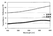
- the spectral reflectance characteristics and the spectral transmittance characteristics of the ND filter manufactured as described above are shown in FIG.
- the concentration is about 0.70, and the reflectance is 0.4% or less in most of the visible wavelength region. With this configuration, very low reflectance could be realized.
- a spectrophotometer (U4100 manufactured by Hitachi High-Technologies Corporation) was used.
- the spectral transmission characteristics are flat over the entire visible region, and one indicator of this flatness is ⁇ (maximum of transmittance at 400 to 700 nm)-(minimum of transmittance at 400 to 700 nm) ⁇
- ⁇ maximum of transmittance at 400 to 700 nm
- minimum of transmittance at 400 to 700 nm In the case where .chi. (Average value of transmittance at 500 to 600 nm) is defined as flatness, the flatness of the filter produced in this example is about 2.5%. It was possible to obtain an ND filter with excellent flatness while suppressing the reflectance in the visible light region to a very low value of 0.5% or less.
- a thin film with high density can be stably formed as compared to the evaporation method or the like.
- an oxide is used to control the refractive index
- a nitride may be used, and various compounds can be used as the gradient refractive index thin film if the refractive index changes continuously and periodically.
- a buffer layer may be provided between the substrate and the gradient refractive index thin film and / or between the gradient refractive index thin film and the anti-reflection structure to improve adhesion and durability. In that case, design may be performed in consideration of the buffer layer.
- the refractive index of the buffer layer is the same as that of the substrate or the antireflective structure adjacent thereto, or the difference in refractive index is made to be close, preferably, the difference in refractive index is 0.05 or less.
- Such a buffer layer can be similarly used in a structure having another gradient index thin film shown in FIG.
- an adhesion layer in the case of providing an adhesion layer as a buffer layer, in addition to silane coupling agents, inorganic materials such as Cr, Ti, TiOx, TiNx, SiOx, SiNx, AlOx, SiOxNy, and various organic substances Materials can be mentioned.
- a material for forming an adhesion layer can be appropriately selected and used from known materials in accordance with the material of the layer for enhancing adhesion.
- the film thickness of the adhesion layer may be set so as to obtain the desired optical function and adhesion of the filter.
- the adhesion layer may be formed, for example, as a thin film of 10 nm or less.
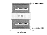
- Example 4 The preparation of a filter having a gradient index thin film formed on both sides of the substrate as shown in FIG. 16 will be described below.
- the refractive index gradient thin film 221 is disposed on one side (upper surface) side of the substrate 23, and the antireflective structure 211 is disposed on the refractive index gradient thin film 221.
- the gradient refractive index thin film 222 another gradient refractive index thin film
- the anti-reflection structure 212 another anti-reflection structure
- the function to have the desired absorption in the desired wavelength range in the ND filter 24 is given to both of the refractive index gradient thin films 221 and 222. In some cases, it is possible to obtain similar characteristics even if only one of the refractive index gradient thin films 221 and 222 is used.
- such anti-reflection structures 211 and 212 include fine periodic structures 251 and 252 having an anti-reflection effect, and a single layer or a plurality of layers.
- the anti-reflective films 261 and 262 formed with the thin film can be mentioned.
- FIG. 17C a configuration in which the fine periodic structure 25 and the antireflective film 26 are used in combination may be mentioned. An optimal configuration may be selected appropriately.
- FIGS. 17 (a) to 17 (c) it is more preferable to use the configuration as shown in FIG. 17 (a) from the viewpoint of reducing the reflection. Therefore, in the present embodiment, as shown in FIG. 17A, the fine periodic structures 251 and 252 are formed on both sides of the substrate 23 as the anti-reflection structure.
- a 1.0 mm thick SFL-6 glass was used as the substrate 23 for forming the ND filter 24.
- the gradient index thin film 221 was produced on one surface side of the substrate 23 by the meta mode sputtering method while adjusting the film forming rate of the SiO 2 and TiO x films. Also in this case, these two types were mixed, and the refractive index was changed continuously in the film thickness direction, so as to obtain desired absorption characteristics. Thereafter, the front and back of the substrate were changed, and a gradient index thin film 222, which is a mixed film of SiO 2 and TiO x again, was produced again. Further, the film thickness of the refractive index gradient thin films 221 and 222 was adjusted to be 200 nm.
- the absorption characteristics in the gradient refractive index thin films 221 and 222 are adjusted by changing x of TiOx in the film thickness direction and changing the extinction coefficient.
- the film was designed so that the spectral transmission characteristics in the visible wavelength region of 400 nm to 700 nm would be flat characteristics with small dispersion as a whole film. That is, the gradient refractive index thin films 221 and 222 are configured to have a refractive index profile as shown in FIG. Although it is possible to form the profile shown in FIG. 18 (b) in which a plurality of hills and valleys in FIG. 12 (a) are formed, it is necessary to prevent complication due to ease of control and the like. It was designed to be an increase or decrease.
- x of TiO x is fixed at about 1.0 from the interface point Q 0 on the substrate side to the point Q 1, and continuous by changing the composition ratio with SiO 2 Form a refractive index change.
- x of TiO x is continuously changed from 1.0 to 1.5.
- the composition ratio to SiO 2 is changed, and the composition ratio of SiO 2 to TiOx is increased as it approaches point Q 2 from point Q 1, and the composition ratio of SiO 2 to TiO x as it approaches point Q 3 from point Q 2 .
- x of TiO x is fixed at about 1.5, and a continuous change in refractive index is formed by changing the composition ratio with SiO 2 .
- the spectral transmission largely influenced by TiO is shown, and in the vicinity of the point Q3, the spectral transmission largely influenced by Ti 2 O 3 is shown. Therefore, by configuring in this way, in the refractive index gradient thin film, regions having different dispersion characteristics as illustrated in FIG. 6 in the visible wavelength region are mixed, and the degree of influence is adjusted by the film thickness and composition ratio. Thus, it is possible to obtain desired transmission characteristics. In the present embodiment, these were adjusted so that the spectral transmission characteristics had a flat shape in the visible wavelength region.
- the refractive index gradient thin film has a gradual increase in refractive index from the side closer to the substrate, passes through the inflection point, and refraction of the antireflective structure toward the antireflective structure It is preferable to approach the rate gently.
- the change in refractive index be as small as possible in the gradient refractive index thin film.
- the difference in refractive index between the substrate 23 and the anti-reflection structure fine periodic structure 251, 252
- the inflection point where the refractive index is the largest among the plurality of inflection points is used as the substrate. It was set to the closest side.
- a submicron pitch fine periodic structure 251, 252 having an antireflection effect is formed by a photo nanoimprinting method using a UV curable resin.
- molds for imprinting were respectively disposed on both sides of the substrate on which the ND film was formed, and both sides were simultaneously subjected to optical nanoimprinting.
- a primer layer was provided between the gradient refractive index thin film and the fine periodic structure corresponding to the gradient refractive index thin film to provide an adhesive layer.
- FIG. 19 shows the spectral reflectance characteristics and the spectral transmittance characteristics of the ND filter manufactured as described above.
- the concentration is about 0.70, and the reflectance is about 0.2% or less in the visible wavelength region. With this configuration, very low reflectance could be realized.
- a spectrophotometer was used for the measurement.
- the spectral transmission characteristics are flat over the entire visible region, and the flatness of the filter manufactured in this example is about 0.5% when converted to the above-described index of flatness, and the visible light region is With the reflectance reduced to a very low value of 0.5% or less, it was possible to obtain a filter with excellent flatness.
- a mixed film of SiO 2 and TiO x was prepared by meta-mode sputtering, and the mixing ratio was changed in the film thickness direction to form a graded thin film having a continuous refractive index.
- various metal or metalloid oxide materials such as NbOx, TaOx, ZrOx, AlOx, MoSiOx, MoOx, and WOx. From the relationship between the refractive index of the refractive index thin film and the structure that forms an interface, as described above, any material that can realize the required refractive index may be used. You can select the material. Further, materials containing elements of three or more metals or metalloids may be combined.
- the inclined thin film by controlling the introduced gas and controlling the refractive index and the extinction coefficient.
- a configuration may be adopted in which absorption is given to a part of the inclined thin film in the film thickness direction, or the refractive index may be changed continuously while having absorption as a whole.
- the film formation method is not limited to the meta mode sputtering method, and may be another sputtering method, various vapor deposition methods, or the like.
- the graded refractive index thin film formed as in this embodiment is a high density film, and film stress may be a problem.
- film stress may be a problem.
- a substrate such as glass with high rigidity
- defects such as warpage due to film stress can be reduced.
- the gradient refractive index thin film on both sides of the substrate, it is possible to manufacture an optical filter which cancels out each film stress and is stable.
- the configuration in which the gradient refractive index thin film and the fine periodic structure are provided on both sides of the substrate used in the present embodiment can obtain the stability of the substrate against film stress.
- the fine periodic structure can be formed on both sides by photo nanoimprinting, so that the antireflective structure can be formed in a series of continuous or simultaneous steps, which is excellent in productivity.
- FIG. 20 shows a light quantity stop device.
- a diaphragm of a light amount diaphragm suitable for use in a photographing optical system such as a video camera or a digital still camera is provided to control the amount of light incident on a solid-state imaging device such as a CCD or CMOS sensor. .
- the diaphragm blade 31 is controlled to be narrowed down to a smaller size.
- the ND filter 34 is disposed in the vicinity of the aperture to make the aperture of the aperture larger even if the brightness of the field is the same. ing. Incident light passes through the light quantity stop device 33 and reaches a solid-state imaging device (not shown), thereby being converted into an electrical signal to form an image.
- the ND filters manufactured in the first to fourth embodiments are disposed at the position of, for example, the ND filter 34 in the stop device 33.
- the arrangement location is not limited to this, and it is possible to arrange so as to be fixed to the diaphragm blade support plate 32.
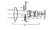
- FIG. 21 shows the structure of the photographing optical system of the optical photographing apparatus.
- the photographing optical system 41 includes lens units 41A to 41D, a solid-state imaging device 42 such as a CCD, and an optical low pass filter 43.
- the solid-state imaging device 42 receives the images of the light beams a and b formed by the photographing optical system 41 and converts them into electric signals.
- the photographing optical system 41 has a light quantity stop device constituted by the ND filter 44, the stop blades 45 and 46, and the stop blade supporting plate 47.
- a diaphragm of a light amount diaphragm suitable for use in a photographing system such as a video camera or a digital still camera is provided to control the amount of light incident on a solid-state imaging device such as a CCD or CMOS sensor.
- a solid-state imaging device such as a CCD or CMOS sensor.
- the aperture blades 45 and 46 are controlled to be narrowed down to a smaller size.
- the ND filter 44 is disposed in the vicinity of the aperture to make the aperture of the aperture larger even if the brightness of the field is the same. ing.
- Incident light passes through the light quantity stop device and reaches the solid-state imaging device, thereby being converted into an electrical signal to form an image.
- the ND filters fabricated in the first to fourth embodiments are disposed at the position of, for example, the ND filter 44 in the stop device.
- the arrangement location is not limited to this, and it is possible to arrange so as to be fixed to the diaphragm blade support plate 47.
- the configuration of the above-described embodiment it is possible to provide an imaging device equipped with an ND filter capable of reducing the possibility of temporal change of a captured image.
- the ND filter using the gradient index thin film prepared in the present Examples 1 to 4 as the ND filter 44 the color balance is different even when the image taken after assembly and the image one month after assembly are compared Did not recognize.
- the ND filter 23 of the optical multilayer film configuration prepared in Comparative Example 1 of FIG. 9 was mounted as the ND filter 44, and images photographed by an optical device using the ND filter 44 were evaluated. As a result, when the image photographed immediately after the assembly of the optical device was compared with the image photographed the same object one month after the assembly, the color balance was different.
- the ND filter of the present invention improves environmental stability, so that the quality of the photographed image can be maintained by using it in an optical photographing apparatus such as a camera or a video camera, which has a large change in the environment carried and used. it can.
- the light quantity stop device 33 manufactured in this manner can significantly reduce problems such as ghosting caused by the reflection of the filter, and can simultaneously achieve, for example, improvement of color balance caused by the transmission characteristics. It is.
- the imaging optical system is provided with the fine periodic structure and the refractive index gradient thin film both sides described in the fourth embodiment in the photographing optical system, reflection on the CCD etc. can be suppressed and a good photographed image can be obtained. It can be assembled without considering the directionality of installation, and it is excellent in assemblability.
- FIG. 22 shows the function and configuration of an interference microscope which is an optical measuring device.
- the light source 910 outputs a predetermined wavelength as a light source. Only constant wavelength components are extracted by the filter 911 from the observation light output from the light source 910. Thereafter, the amount of light of the observation light is appropriately adjusted via the ND filter 912 selectively disposed on the light path in accordance with the rotational position of the filter holder 913 holding the ND filter 912 having different transmittances.
- a light source a laser light source of monochromatic wavelength or the like can also be used as a light source.
- the filter holder 913 arranges a plurality of ND filters 912 each having different transmittances, and operates the rotation drive unit 914 based on control from a CPU (not shown) or the like to drive any one of the transmittance ND filters 912 is selectively placed on the light path. If the spot diameter of the light source and the gradation range correspond to each other, the transmittance may be changed by positioning of the gradation ND filter. In such a case, the ND filter may be configured to operate as in the diaphragm device shown in the fifth embodiment. The light having passed through the ND filter 912 has its polarization angle changed through the polarizing plate 915 similarly disposed on the light path.
- the polarizing plate 915 changes the polarization angle of the transmitted light to a desired angle by being rotationally driven by the polarizing plate rotational drive unit 916, and the polarizing plate rotational drive unit 916 is also from the CPU or the like. Operate based on the control of
- the light passing through the polarizing plate 915 is reflected by the half mirror 917 toward the sample, and then split by the prism 918 into two parallel optical paths according to the polarization direction.
- the light split into the two optical paths is both irradiated via the objective lens 919 to the observation object 920 mounted on the focus observation mechanism 921 for adjusting the focus.
- the light reflected from the observation object 920 passes through the half mirror 917 via the objective lens 919 and the prism 918, and is imaged on the imaging device 924 such as a CCD by the imaging lens 922.
- An analyzer 923 as a rotatable polarizing element is disposed on the light path between the imaging lens 922 and the imaging element 924.
- the output of the image sensor 924 is converted into a digital signal, and a surface structure, a refractive index distribution, and the like can be analyzed by analyzing interference fringes processed and observed by a CPU or the like.
- the optical measuring apparatus is not limited to the present embodiment, and by using the ND filter of the present invention, it is possible to use the ND measuring apparatus as an optical apparatus which is an optical device that requires long-term reliability of measurement accuracy. It is possible to perform the measurement while suppressing the adverse effect due to the temporal change of the filter. As a result, it is possible to improve the stability of image quality such as interference fringes which are images taken by an optical device such as an optical measuring device that may be adversely affected by long-term use.
- optical filters other than the ND filters described in the first to fourth embodiments also in the optical filters other than the ND filters described in the first to fourth embodiments, similar effects can be expected as long as they are optical filters of the type having absorption and the issue of flatness of transmitted light is an issue. Things are possible.
- By applying the present invention to these optical filters it is possible to obtain desired transmission characteristics while reducing the reflectance. Further, by mounting these optical filters, it becomes possible to obtain various optical devices in which the above-mentioned problems are improved.
Abstract
Description
(1)前記基板側において、前記屈折率変化の前記基板側の終点まで、前記屈折率が前記基板の屈折率に近づくように変化する部分と、
(2)前記反射防止構造体側において、前記屈折率変化の前記反射防止構造体側の終点まで、前記屈折率が前記反射防止構造体の屈折率に近づくように変化する部分と
を有することが好ましい。 The graded refractive index thin film has a change in refractive index that changes continuously and periodically in the thickness direction. The refractive index change of the graded refractive index thin film in the optical filter having the substrate, the graded refractive index thin film and the antireflective structure is
(1) A portion on the substrate side where the refractive index changes so as to approach the refractive index of the substrate up to the end point on the substrate side of the refractive index change;
(2) On the side of the antireflective structure, it is preferable to have a portion where the refractive index changes so as to approach the refractive index of the antireflective structure until the end point of the change of the refractive index on the side of the antireflective structure.
図2のように構成した、吸収タイプのNDフィルタについて、以下に詳しく記載する。 (Embodiment 1)
The absorption type ND filter configured as shown in FIG. 2 will be described in detail below.
屈折率傾斜薄膜12は、メタモードスパッタ法により、SiO2とTiOx膜の成膜レートを調整しながら、この2種類を混合させ、屈折率を膜厚方向で連続的に変化させる事で、所望の吸収特性を得るように調整し作製した。 <About the refractive index gradient thin film>
The gradient refractive index thin film 12 is desirably formed by mixing the two types while adjusting the film formation rate of the SiO 2 film and the TiO x film by the meta mode sputtering method and continuously changing the refractive index in the film thickness direction. Prepared to obtain the absorption characteristics of
図7は、屈折率傾斜薄膜の作製に用いたスパッタ成膜装置の基板搬送装置の回転軸に直交する面での平面断面図である。 <Sputtering device configuration>
FIG. 7 is a plan cross-sectional view in a plane orthogonal to the rotation axis of the substrate transfer device of the sputtering film forming apparatus used for producing the gradient refractive index thin film.
図2のように構成した、吸収タイプのNDフィルタについて、以下に詳しく記載する。本実施例では、基板13の片面側に、薄膜中の少なくても一部に吸収を持つ屈折率傾斜薄膜12を配置した。反射防止構造体は設けない構成とした。 Example 1
The absorption type ND filter configured as shown in FIG. 2 will be described in detail below. In this embodiment, the gradient index thin film 12 having absorption in at least a part of the thin film is disposed on one side of the substrate 13. The anti-reflection structure was not provided.
実施例1での環境安定性の効果を考察する為に、図8と略同様となる分光透過率特性を多層膜構成を用いて、膜厚200nmで作製し、その他材料やプロセスは可能な限り実施例1と同様となるように作製したNDフィルタ4について以下に記載する。 (Comparative example 1)
In order to consider the effect of environmental stability in Example 1, a spectral transmittance characteristic substantially similar to that of FIG. 8 is produced with a film thickness of 200 nm using a multilayer film configuration, and other materials and processes are as much as possible. The ND filter 4 manufactured to be similar to that of the first embodiment will be described below.
実施例1と同様に基板13には厚さ1.0mmのSFL-6ガラスを用い、基板13と屈折率傾斜薄膜12からなるNDフィルタを作製した。屈折率傾斜薄膜12は膜厚が200nmとなるように、メタモードスパッタ法により、SiO2とTiOx膜の成膜レートを調整しながら、この2種類を混合させ、連続的に組成を変化させる事で、屈折率を膜厚方向で連続的に変化させ、所望の吸収特性を得るように調整し作製した。これに加え、TiOxのxを変化させる事で、可視波長領域における分光透過率が、長波長側になるにつれ高くなる領域と、長波長側になるにつれ低くなる領域とを、屈折率傾斜薄膜12中に設ける構成とした。このように、特定の波長領域における分光透過率において、同一膜中に相反する分散形状を持つ領域を設ける事で、例えばNDフィルタであれば、より波長分散の小さい、より平坦な分光透過特性を得る事が可能となる。 (Example 2)
In the same manner as in Example 1, a 1.0 mm thick SFL-6 glass was used as the substrate 13, and an ND filter composed of the substrate 13 and the gradient refractive index thin film 12 was produced. The composition of the graded refractive index thin film 12 is continuously mixed by mixing these two types while adjusting the film forming rate of the SiO 2 and TiO x films by meta mode sputtering so that the film thickness becomes 200 nm. The refractive index was continuously changed in the film thickness direction, and was adjusted and manufactured so as to obtain a desired absorption characteristic. In addition to this, by changing x of TiOx, the refractive index gradient thin film 12 is a region in which the spectral transmittance in the visible wavelength region becomes higher as it goes to the long wavelength side and a region that becomes lower as it goes to the long wavelength side. It was set up in the inside. As described above, by providing regions having opposite dispersion shapes in the same film in the spectral transmittance in a specific wavelength region, for example, in the case of an ND filter, a flatter spectral transmission characteristic with smaller wavelength dispersion. It is possible to get.
<反射防止構造体について>
基板13上に屈折率傾斜薄膜12の形成後、UV硬化性樹脂を用いた光ナノインプリント法により、屈折率傾斜薄膜12上に、反射防止効果を持つサブミクロンピッチの反射防止構造体としての微細周期構造体151と152を形成した。 (Example 3)
<Regarding anti-reflection structure>
After forming the gradient refractive index thin film 12 on the substrate 13, a fine cycle as a submicron pitch antireflective structure having an antireflective effect on the gradient refractive index thin film 12 by photo nanoimprinting using a UV curable resin Structures 151 and 152 were formed.
このような構造体の1つである、反射防止効果を持つ微細周期構造体は、一般的にモス・アイ構造体などと呼ぶことも可能である。構造体の形状を擬似的に屈折率の変化が連続的となる形状とする事で、物質間の屈折率差に起因した反射の低減を図ったものである。 The fine periodic structure has come to be manufactured with the improvement of the micro processing technology in recent years.
One of such structures, a fine periodic structure having an antireflective effect, can also be generally called a moth-eye structure or the like. By making the shape of the structure into a shape in which the change of the refractive index is pseudo-continuous, it is intended to reduce the reflection due to the refractive index difference between the substances.
以上によって作製されたNDフィルタの、分光反射率特性、及び分光透過率特性が図15である。濃度は約0.70程度であり、可視波長領域の殆どにおいて反射率が0.4%以下になっている。本構成により、非常に低い反射率を実現できた。測定には、分光光度計(U4100(株)日立ハイテクノロジーズ社製)を用いた。 <Characteristics of optical filter>
The spectral reflectance characteristics and the spectral transmittance characteristics of the ND filter manufactured as described above are shown in FIG. The concentration is about 0.70, and the reflectance is 0.4% or less in most of the visible wavelength region. With this configuration, very low reflectance could be realized. For measurement, a spectrophotometer (U4100 manufactured by Hitachi High-Technologies Corporation) was used.
図16のように基板両面に屈折率傾斜薄膜を形成したフィルタの作製について以下に記載する。 (Example 4)
The preparation of a filter having a gradient index thin film formed on both sides of the substrate as shown in FIG. 16 will be described below.
図20に光量絞り装置を示す。ビデオカメラあるいはデジタルスチルカメラ等の撮影光学系に使用するに適した光量絞り装置の絞りは、CCDやCMOSセンサと言った固体撮像素子への入射光量を制御するために設けられているものである。被写界が明るくなるにつれ、絞り羽根31を制御し、より小さく絞り込まれていく構造になっている。このとき、小絞り状態時に発生する像性能の劣化に対する対策として、絞りの近傍にNDフィルタ34を配置し、被写界の明るさが同一であっても、絞りの開口をより大きくできる構造にしている。入射光がこの光量絞り装置33を通過し、固体撮像素子(不図示)に到達する事で電気的な信号に変換され画像が形成される。 (Example 5)
FIG. 20 shows a light quantity stop device. A diaphragm of a light amount diaphragm suitable for use in a photographing optical system such as a video camera or a digital still camera is provided to control the amount of light incident on a solid-state imaging device such as a CCD or CMOS sensor. . As the field becomes brighter, the
図22は光学測定装置である干渉顕微鏡の機能及び構成を示す。光源910は光源として所定の波長を出力する。この光源910から出力された観察光から、フィルタ911にて一定の波長成分のみが抽出される。その後、観察光は、それぞれ異なる透過率を有するNDフィルタ912を保持したフィルタホルダ913の回転位置に応じて選択的に光路上に配置されたNDフィルタ912を介して、適宜光量が調節される。光源としては、単色波長のレーザ光源等も光源として用いることができる。 (Example 6)
FIG. 22 shows the function and configuration of an interference microscope which is an optical measuring device. The
実施例1~4で記載したNDフィルタ以外の光学フィルタにおいても、吸収を持つタイプで透過光の平坦性を課題とする光学フィルタであれば同様の効果を期待でき、例えばカラーフィルタなどに応用する事が可能である。これらの光学フィルタに本発明を適用する事で、反射率を低減しつつ、所望の透過特性を得る事が可能となる。また、これらの光学フィルタを搭載する事で、前述の不具合を改善した各種の光学装置を得る事が可能となる。 (Other embodiments)
Also in the optical filters other than the ND filters described in the first to fourth embodiments, similar effects can be expected as long as they are optical filters of the type having absorption and the issue of flatness of transmitted light is an issue. Things are possible. By applying the present invention to these optical filters, it is possible to obtain desired transmission characteristics while reducing the reflectance. Further, by mounting these optical filters, it becomes possible to obtain various optical devices in which the above-mentioned problems are improved.
12、221、222.屈折率傾斜薄膜
3、13、23、51.基板
15、151、152、251、252.微細周期構造体
16、161、162.反射防止膜
31.絞り羽根
32.絞り羽根支持板
33.光量絞り装置
4、14、24、34.44、912.NDフィルタ
41.撮影光学系
41A、41B、41C、41D.レンズユニット
42.固体撮像素子
43.光学ローパスフィルタ
45、46.絞り羽根
52.基板搬送装置
53.真空槽
54,55.スパッタ領域
54a、55a.ターゲット
56.高周波電源
57.反応領域 111, 112, 211, 212. Anti-reflection structures 12, 221, 222. Refractive index gradient
41A, 41B, 41C, 41D. Lens unit
42. Solid-state image sensor
43. Optical low pass filter
45, 46. Aperture blade
52.
Claims (13)
- 光透過性を有する基板と、
膜厚方向に前記基板側へ向かって前記基板の屈折率に近づくように屈折率変化する光吸収性の屈折率傾斜薄膜と、
を備えたことを特徴とする光学フィルタ。 A light transmitting substrate,
A light absorbing gradient refractive index thin film whose refractive index changes so as to approach the refractive index of the substrate toward the substrate in the film thickness direction;
An optical filter characterized by comprising. - 前記屈折率傾斜薄膜は、その膜厚方向において、
可視波長領域の分光透過特性が長波長側になるにつれて高くなる領域と、
可視波長領域の分光透過特性が長波長側になるにつれて低くなる領域と、
を有することを特徴とする請求項1に記載の光学フィルタ。 In the film thickness direction, the refractive index gradient thin film is
A region where the spectral transmission characteristics in the visible wavelength region become higher as the wavelength becomes longer;
An area where spectral transmission characteristics in the visible wavelength range become lower as the wavelength becomes longer,
The optical filter according to claim 1, comprising: - 前記屈折率傾斜薄膜を構成する物質の組成は、前記膜厚方向に連続的に変化することを特徴とする請求項1または請求項2に記載の光学フィルタ。 3. The optical filter according to claim 1, wherein the composition of the material constituting the gradient refractive index thin film changes continuously in the film thickness direction.
- 前記屈折率傾斜薄膜の前記基板側とは反対側の面の上に反射防止構造体を備え、
前記屈折率傾斜薄膜は、前記基板の屈折率と前記反射防止構造体の屈折率との屈折率差を低減するように膜厚方向に屈折率変化することを特徴とする請求項1~3のいずれか一項に記載の光学フィルタ。 An anti-reflection structure is provided on the surface of the gradient index thin film opposite to the substrate side,
The refractive index change in the film thickness direction is carried out so that the refractive index gradient thin film reduces the difference in refractive index between the refractive index of the substrate and the refractive index of the anti-reflection structure. The optical filter as described in any one. - 前記反射防止構造体は、可視光の波長よりも短いピッチの微細構造体であることを特徴とする請求項4に記載の光学フィルタ。 5. The optical filter according to claim 4, wherein the anti-reflection structure is a fine structure having a pitch shorter than the wavelength of visible light.
- 前記基板の前記反射防止構造体側とは反対側の面の上に、他の反射防止構造体を備えたことを特徴とする請求項4または請求項5に記載の光学フィルタ。 The optical filter according to claim 4 or 5, further comprising another anti-reflection structure on the surface of the substrate opposite to the anti-reflection structure side.
- 前記基板と前記他の反射防止構造体との間に前記他の反射防止構造体の屈折率と前記基板の屈折率との屈折率差を低減するように膜厚方向に屈折率変化する他の屈折率傾斜薄膜を備えたことを特徴とする請求項6に記載の光学フィルタ。 The refractive index changes in the film thickness direction so as to reduce the difference in refractive index between the refractive index of the other antireflective structure and the refractive index of the substrate between the substrate and the other antireflective structure 7. The optical filter according to claim 6, further comprising a gradient index thin film.
- 前記他の反射防止構造体は、単層又は複数層の反射防止膜であり、前記他の屈折率傾斜薄膜は、前記反射防止膜の前記他の屈折率傾斜薄膜に隣接する層の屈折率と前記基板の屈折率との屈折率差を低減するように、前記膜厚方向に屈折率変化することを特徴とする請求項7に記載の光学フィルタ。 The other antireflective structure is a single layer or multiple layers of antireflective film, and the other refractive index gradient thin film is a refractive index of a layer adjacent to the other refractive index gradient thin film of the antireflective film and The optical filter according to claim 7, wherein the refractive index changes in the film thickness direction so as to reduce the difference in refractive index with the refractive index of the substrate.
- 前記第2の反射防止構造体は、可視光の波長よりも短いピッチの微細構造体であることを特徴とする請求項7に記載の光学フィルタ。 8. The optical filter according to claim 7, wherein the second antireflective structure is a fine structure having a pitch shorter than the wavelength of visible light.
- 前記屈折率傾斜薄膜が3種類以上の元素から構成されている事を特徴とする請求項1~6いずれか一項に記載の光学フィルタ。 The optical filter according to any one of claims 1 to 6, wherein the gradient refractive index thin film is composed of three or more types of elements.
- 前記屈折率傾斜薄膜の基板側の屈折率変化の終点と前記基板との屈折率差は、0.05より小さいことを特徴とする請求項1~6のいずれか一項に記載の光学フィルタ。 The optical filter according to any one of claims 1 to 6, wherein the refractive index difference between the end point of the refractive index change on the substrate side of the gradient refractive index thin film and the substrate is smaller than 0.05.
- 前記微細構造体は、可視光の波長よりも短いピッチの周期構造を有することを特徴とする請求項1~11のいずれか一項に記載の光学フィルタ。 The optical filter according to any one of claims 1 to 11, wherein the microstructure has a periodic structure with a pitch shorter than the wavelength of visible light.
- 請求項1~12のいずれか一項に記載の光学フィルタを撮影光学系に備えたことを特徴とする光学装置。 An optical apparatus comprising the optical filter according to any one of claims 1 to 12 in a photographing optical system.
Priority Applications (4)
| Application Number | Priority Date | Filing Date | Title |
|---|---|---|---|
| JP2013515200A JP5728572B2 (en) | 2011-05-17 | 2012-05-17 | Optical filter and optical device |
| EP12785144.2A EP2711744A4 (en) | 2011-05-17 | 2012-05-17 | Optical filter and optical device |
| US14/118,002 US9588266B2 (en) | 2011-05-17 | 2012-05-17 | Optical filter and optical apparatus |
| CN201280035495.0A CN103688195B (en) | 2011-05-17 | 2012-05-17 | Optical filter and optical device |
Applications Claiming Priority (4)
| Application Number | Priority Date | Filing Date | Title |
|---|---|---|---|
| JP2011-110595 | 2011-05-17 | ||
| JP2011110595 | 2011-05-17 | ||
| JP2011-128757 | 2011-06-09 | ||
| JP2011128757 | 2011-06-09 |
Publications (1)
| Publication Number | Publication Date |
|---|---|
| WO2012157719A1 true WO2012157719A1 (en) | 2012-11-22 |
Family
ID=47177036
Family Applications (1)
| Application Number | Title | Priority Date | Filing Date |
|---|---|---|---|
| PCT/JP2012/062700 WO2012157719A1 (en) | 2011-05-17 | 2012-05-17 | Optical filter and optical device |
Country Status (5)
| Country | Link |
|---|---|
| US (1) | US9588266B2 (en) |
| EP (1) | EP2711744A4 (en) |
| JP (1) | JP5728572B2 (en) |
| CN (1) | CN103688195B (en) |
| WO (1) | WO2012157719A1 (en) |
Cited By (16)
| Publication number | Priority date | Publication date | Assignee | Title |
|---|---|---|---|---|
| WO2014077399A1 (en) * | 2012-11-16 | 2014-05-22 | キヤノン電子株式会社 | Optical filter and optical apparatus |
| JP2014102297A (en) * | 2012-11-16 | 2014-06-05 | Canon Electronics Inc | Optical filter and optical equipment |
| CN104658982A (en) * | 2013-11-21 | 2015-05-27 | 昆山中辰矽晶有限公司 | Optical assembly and method of manufacturing the same |
| WO2015100981A1 (en) * | 2013-12-30 | 2015-07-09 | 京东方科技集团股份有限公司 | Array substrate and display device |
| EP2994783A1 (en) * | 2013-05-07 | 2016-03-16 | Corning Incorporated | Scratch-resistant articles with a gradient layer |
| EP3006969A4 (en) * | 2013-06-03 | 2016-06-08 | Fujifilm Corp | Optical member provided with anti-reflection film |
| JP2016139138A (en) * | 2015-01-27 | 2016-08-04 | フラウンホーファー−ゲゼルシャフト ツル フェルデルング デル アンゲヴァンテン フォルシュング エー ファウFraunhofer−Gesellschaft zur Foerderung der angewandten Forschung e.V. | Method of producing reflection-reducing layer system, and reflection-reducing layer system |
| WO2020066428A1 (en) * | 2018-09-27 | 2020-04-02 | 富士フイルム株式会社 | Antireflection film, optical element, method for producing antireflection film, and method for producing fine relief structure |
| US10948629B2 (en) | 2018-08-17 | 2021-03-16 | Corning Incorporated | Inorganic oxide articles with thin, durable anti-reflective structures |
| US10995404B2 (en) | 2014-08-01 | 2021-05-04 | Corning Incorporated | Scratch-resistant materials and articles including the same |
| US11002885B2 (en) | 2015-09-14 | 2021-05-11 | Corning Incorporated | Scratch-resistant anti-reflective articles |
| US11231526B2 (en) | 2013-05-07 | 2022-01-25 | Corning Incorporated | Low-color scratch-resistant articles with a multilayer optical film |
| US11267973B2 (en) | 2014-05-12 | 2022-03-08 | Corning Incorporated | Durable anti-reflective articles |
| JP2022121418A (en) * | 2021-02-08 | 2022-08-19 | 東海光学株式会社 | Optical product |
| JP2023015187A (en) * | 2021-02-08 | 2023-01-31 | 東海光学株式会社 | Optical product |
| US11667565B2 (en) | 2013-05-07 | 2023-06-06 | Corning Incorporated | Scratch-resistant laminates with retained optical properties |
Families Citing this family (18)
| Publication number | Priority date | Publication date | Assignee | Title |
|---|---|---|---|---|
| JP6006718B2 (en) * | 2011-05-17 | 2016-10-12 | キヤノン電子株式会社 | Optical filter, optical device, electronic device, and antireflection composite |
| JP6249950B2 (en) | 2012-08-31 | 2017-12-20 | キヤノン電子株式会社 | Light amount adjusting device, imaging optical system, and imaging device |
| CN106574982B (en) | 2014-04-28 | 2019-09-17 | 蒙特利尔综合理工学院公司 | Thermo-mechanical property with optimization, the article including titanium-organic nature layer |
| CN106662673B (en) * | 2014-07-10 | 2018-11-30 | Scivax股份有限公司 | Optical component and its manufacturing method |
| TWI570496B (en) | 2014-12-10 | 2017-02-11 | 元太科技工業股份有限公司 | Reflective display device |
| WO2016104590A1 (en) * | 2014-12-26 | 2016-06-30 | 旭硝子株式会社 | Optical filter and image pickup device |
| JP6316768B2 (en) * | 2015-03-26 | 2018-04-25 | 東京エレクトロン株式会社 | Adhesion layer forming method, adhesion layer forming system, and storage medium |
| WO2017038213A1 (en) * | 2015-08-31 | 2017-03-09 | Hoya株式会社 | Mask blank, phase shift mask, phase shift mask manufacturing method, and semiconductor device manufacturing method |
| KR102404648B1 (en) * | 2015-09-21 | 2022-05-31 | 엘지디스플레이 주식회사 | Display device |
| JP6991706B2 (en) * | 2016-11-30 | 2022-02-03 | キヤノン株式会社 | Optical element and optical system having it |
| CN106772741B (en) * | 2016-12-05 | 2019-07-23 | 江南大学 | A method of guide mode resonance filtering is realized using single graded material grating |
| DE102017105372B4 (en) * | 2017-03-14 | 2022-05-25 | Schott Ag | Transparent element with an anti-reflective coating and method of making same |
| US10708537B2 (en) * | 2018-07-28 | 2020-07-07 | Haas Laser Technologies, Inc. | System and method for reducing ghost images in a laser imaging system |
| US10976477B2 (en) * | 2018-08-31 | 2021-04-13 | Samsung Electronics Co., Ltd. | Optical filter and spectrometer including sub-wavelength reflector, and electronic apparatus including the spectrometer |
| CN109445010B (en) * | 2019-01-15 | 2024-03-29 | 北极光电(深圳)有限公司 | Improved stress type filter structure and wavelength division multiplexer |
| JP7340173B2 (en) * | 2019-03-05 | 2023-09-07 | 東洋アルミニウム株式会社 | Black aluminum pigment and its manufacturing method |
| US11314004B2 (en) | 2019-04-08 | 2022-04-26 | Visera Technologies Company Limited | Optical filters and methods for forming the same |
| CN114431825B (en) * | 2022-04-12 | 2022-06-21 | 万灵帮桥医疗器械(广州)有限责任公司 | Slit-lamp microscope and filtering adjusting structure thereof |
Citations (9)
| Publication number | Priority date | Publication date | Assignee | Title |
|---|---|---|---|---|
| JPH0763915A (en) * | 1993-08-26 | 1995-03-10 | Canon Inc | Thin film nd filter and its production |
| JPH0875902A (en) | 1994-09-07 | 1996-03-22 | Canon Inc | Multilayer reflection preventing film |
| JPH0883581A (en) * | 1994-09-13 | 1996-03-26 | Hitachi Ltd | Surface plate treatment film and display device and its manufacture |
| JP2002267815A (en) * | 2001-03-08 | 2002-09-18 | Dainippon Printing Co Ltd | Reflection preventive molded part and method for manufacturing the same |
| JP2004212462A (en) * | 2002-12-27 | 2004-07-29 | Canon Electronics Inc | Nd filter for light quantity stopping, light quantity stopping device, camera having same, and method for manufacturing the filter |
| JP2005133131A (en) * | 2003-10-29 | 2005-05-26 | Dainippon Printing Co Ltd | Method for forming refractive-index-changing layer |
| JP2009122216A (en) | 2007-11-13 | 2009-06-04 | Sumitomo Metal Mining Co Ltd | Absorption type nd filter |
| JP2010277094A (en) | 2004-11-24 | 2010-12-09 | Sumitomo Metal Mining Co Ltd | Method for producing absorption type multi-layer film nd filter |
| WO2010150615A1 (en) * | 2009-06-23 | 2010-12-29 | シャープ株式会社 | Display device and multilayer substrate |
Family Cites Families (10)
| Publication number | Priority date | Publication date | Assignee | Title |
|---|---|---|---|---|
| JPS6371801A (en) | 1986-09-16 | 1988-04-01 | Hitachi Ltd | Antireflection film |
| US5283692A (en) * | 1989-07-21 | 1994-02-01 | Spectra Physics Lasers, Inc. | Multi-layer graded reflectivity mirror |
| CN1057611C (en) * | 1993-08-31 | 2000-10-18 | 住友水泥株式会社 | Antireflection film |
| JP3905035B2 (en) * | 2000-08-29 | 2007-04-18 | 独立行政法人科学技術振興機構 | Method for forming optical thin film |
| US7193780B2 (en) | 2003-08-22 | 2007-03-20 | Olympus Corporation | Optical filter and optical instrument |
| CN100595608C (en) * | 2005-02-18 | 2010-03-24 | 佳能株式会社 | Optical transparent member and optical system using the same |
| JP4520418B2 (en) * | 2005-02-18 | 2010-08-04 | キヤノン株式会社 | Optical transparent member and optical system using the same |
| JP4760237B2 (en) * | 2005-09-02 | 2011-08-31 | 株式会社日立製作所 | Optical component and projection-type image display device using the same |
| EP1760497B1 (en) * | 2005-09-02 | 2016-11-09 | Hitachi Maxell, Ltd. | Optical part and projection type display apparatus using same |
| JP6006718B2 (en) | 2011-05-17 | 2016-10-12 | キヤノン電子株式会社 | Optical filter, optical device, electronic device, and antireflection composite |
-
2012
- 2012-05-17 US US14/118,002 patent/US9588266B2/en active Active
- 2012-05-17 WO PCT/JP2012/062700 patent/WO2012157719A1/en active Application Filing
- 2012-05-17 JP JP2013515200A patent/JP5728572B2/en active Active
- 2012-05-17 EP EP12785144.2A patent/EP2711744A4/en not_active Withdrawn
- 2012-05-17 CN CN201280035495.0A patent/CN103688195B/en active Active
Patent Citations (10)
| Publication number | Priority date | Publication date | Assignee | Title |
|---|---|---|---|---|
| JPH0763915A (en) * | 1993-08-26 | 1995-03-10 | Canon Inc | Thin film nd filter and its production |
| JP3359114B2 (en) | 1993-08-26 | 2002-12-24 | キヤノン株式会社 | Thin film type ND filter and method of manufacturing the same |
| JPH0875902A (en) | 1994-09-07 | 1996-03-22 | Canon Inc | Multilayer reflection preventing film |
| JPH0883581A (en) * | 1994-09-13 | 1996-03-26 | Hitachi Ltd | Surface plate treatment film and display device and its manufacture |
| JP2002267815A (en) * | 2001-03-08 | 2002-09-18 | Dainippon Printing Co Ltd | Reflection preventive molded part and method for manufacturing the same |
| JP2004212462A (en) * | 2002-12-27 | 2004-07-29 | Canon Electronics Inc | Nd filter for light quantity stopping, light quantity stopping device, camera having same, and method for manufacturing the filter |
| JP2005133131A (en) * | 2003-10-29 | 2005-05-26 | Dainippon Printing Co Ltd | Method for forming refractive-index-changing layer |
| JP2010277094A (en) | 2004-11-24 | 2010-12-09 | Sumitomo Metal Mining Co Ltd | Method for producing absorption type multi-layer film nd filter |
| JP2009122216A (en) | 2007-11-13 | 2009-06-04 | Sumitomo Metal Mining Co Ltd | Absorption type nd filter |
| WO2010150615A1 (en) * | 2009-06-23 | 2010-12-29 | シャープ株式会社 | Display device and multilayer substrate |
Non-Patent Citations (1)
| Title |
|---|
| See also references of EP2711744A4 |
Cited By (26)
| Publication number | Priority date | Publication date | Assignee | Title |
|---|---|---|---|---|
| WO2014077399A1 (en) * | 2012-11-16 | 2014-05-22 | キヤノン電子株式会社 | Optical filter and optical apparatus |
| JP2014102297A (en) * | 2012-11-16 | 2014-06-05 | Canon Electronics Inc | Optical filter and optical equipment |
| US9513417B2 (en) | 2012-11-16 | 2016-12-06 | Canon Denshi Kabushiki Kaisha | Optical filter and optical apparatus |
| US11714213B2 (en) | 2013-05-07 | 2023-08-01 | Corning Incorporated | Low-color scratch-resistant articles with a multilayer optical film |
| EP2994783A1 (en) * | 2013-05-07 | 2016-03-16 | Corning Incorporated | Scratch-resistant articles with a gradient layer |
| US11231526B2 (en) | 2013-05-07 | 2022-01-25 | Corning Incorporated | Low-color scratch-resistant articles with a multilayer optical film |
| US11667565B2 (en) | 2013-05-07 | 2023-06-06 | Corning Incorporated | Scratch-resistant laminates with retained optical properties |
| EP3006969A4 (en) * | 2013-06-03 | 2016-06-08 | Fujifilm Corp | Optical member provided with anti-reflection film |
| CN104658982A (en) * | 2013-11-21 | 2015-05-27 | 昆山中辰矽晶有限公司 | Optical assembly and method of manufacturing the same |
| WO2015100981A1 (en) * | 2013-12-30 | 2015-07-09 | 京东方科技集团股份有限公司 | Array substrate and display device |
| US9958713B2 (en) | 2013-12-30 | 2018-05-01 | Boe Technology Group Co., Ltd. | Array substrate and display device |
| US11267973B2 (en) | 2014-05-12 | 2022-03-08 | Corning Incorporated | Durable anti-reflective articles |
| US10995404B2 (en) | 2014-08-01 | 2021-05-04 | Corning Incorporated | Scratch-resistant materials and articles including the same |
| JP2016139138A (en) * | 2015-01-27 | 2016-08-04 | フラウンホーファー−ゲゼルシャフト ツル フェルデルング デル アンゲヴァンテン フォルシュング エー ファウFraunhofer−Gesellschaft zur Foerderung der angewandten Forschung e.V. | Method of producing reflection-reducing layer system, and reflection-reducing layer system |
| US10539716B2 (en) | 2015-01-27 | 2020-01-21 | Fraunhofer-Gesellschaft Zur Foerderung Der Angewandten Forschung E.V. | Method for producing a reflection-reducing layer system and reflection-reducing layer system |
| US11002885B2 (en) | 2015-09-14 | 2021-05-11 | Corning Incorporated | Scratch-resistant anti-reflective articles |
| US11698475B2 (en) | 2015-09-14 | 2023-07-11 | Corning Incorporated | Scratch-resistant anti-reflective articles |
| US10948629B2 (en) | 2018-08-17 | 2021-03-16 | Corning Incorporated | Inorganic oxide articles with thin, durable anti-reflective structures |
| US11906699B2 (en) | 2018-08-17 | 2024-02-20 | Corning Incorporated | Inorganic oxide articles with thin, durable anti reflective structures |
| JPWO2020066428A1 (en) * | 2018-09-27 | 2021-09-16 | 富士フイルム株式会社 | Method for manufacturing antireflection film, optical element, antireflection film and method for forming fine uneven structure |
| JP7065995B2 (en) | 2018-09-27 | 2022-05-12 | 富士フイルム株式会社 | Method for manufacturing antireflection film and method for forming fine uneven structure |
| WO2020066428A1 (en) * | 2018-09-27 | 2020-04-02 | 富士フイルム株式会社 | Antireflection film, optical element, method for producing antireflection film, and method for producing fine relief structure |
| JP2022121418A (en) * | 2021-02-08 | 2022-08-19 | 東海光学株式会社 | Optical product |
| JP7188827B2 (en) | 2021-02-08 | 2022-12-13 | 東海光学株式会社 | Optical products for anti-reflection of visible light |
| JP2023015187A (en) * | 2021-02-08 | 2023-01-31 | 東海光学株式会社 | Optical product |
| JP7274799B2 (en) | 2021-02-08 | 2023-05-17 | 東海光学株式会社 | optical products |
Also Published As
| Publication number | Publication date |
|---|---|
| US9588266B2 (en) | 2017-03-07 |
| EP2711744A1 (en) | 2014-03-26 |
| EP2711744A4 (en) | 2014-10-29 |
| JPWO2012157719A1 (en) | 2014-07-31 |
| CN103688195B (en) | 2017-03-08 |
| US20140071552A1 (en) | 2014-03-13 |
| JP5728572B2 (en) | 2015-06-03 |
| CN103688195A (en) | 2014-03-26 |
Similar Documents
| Publication | Publication Date | Title |
|---|---|---|
| WO2012157719A1 (en) | Optical filter and optical device | |
| JP6006718B2 (en) | Optical filter, optical device, electronic device, and antireflection composite | |
| US9513417B2 (en) | Optical filter and optical apparatus | |
| JP6317954B2 (en) | Lens unit, imaging module, and electronic device | |
| JP5789373B2 (en) | Optical filter | |
| JP5819063B2 (en) | Optical filter | |
| JP2013015827A (en) | Nd filter and optical device | |
| JP2012137646A (en) | Optical filter | |
| JP2012137649A (en) | Optical filter | |
| JP2008276059A (en) | Optical element and optical system having the same | |
| JP4801442B2 (en) | ND filter for diaphragm | |
| JP6053352B2 (en) | Optical filter, optical device, and optical filter manufacturing method. | |
| WO2012023372A1 (en) | Optical functional element and imaging device | |
| JP2010066704A (en) | Optical element, optical system, and optical apparatus | |
| JP6162947B2 (en) | Optical filter, optical device, electronic device | |
| JP6556529B2 (en) | Optical filter and optical device provided with optical filter | |
| JP2007171542A (en) | Nd filter for optical diaphragm and optical diaphragm device provided with nd filter | |
| JP6224314B2 (en) | Optical filter and optical apparatus | |
| JP2007316238A (en) | Nd filter | |
| JP6056445B2 (en) | Optical element manufacturing method | |
| JP6980364B2 (en) | Optical filter, light intensity adjuster and optical device | |
| JP6386785B2 (en) | MICROSTRUCTURE, OPTICAL FILTER AND OPTICAL DEVICE | |
| JP2017044944A (en) | Optical filter, light volume adjusting unit, and optical device | |
| JP2017044943A (en) | Antireflection fine structure, optical filter, light volume adjusting unit, and optical device |
Legal Events
| Date | Code | Title | Description |
|---|---|---|---|
| 121 | Ep: the epo has been informed by wipo that ep was designated in this application |
Ref document number: 12785144 Country of ref document: EP Kind code of ref document: A1 |
|
| ENP | Entry into the national phase |
Ref document number: 2013515200 Country of ref document: JP Kind code of ref document: A |
|
| WWE | Wipo information: entry into national phase |
Ref document number: 14118002 Country of ref document: US |
|
| NENP | Non-entry into the national phase |
Ref country code: DE |
|
| REEP | Request for entry into the european phase |
Ref document number: 2012785144 Country of ref document: EP |
|
| WWE | Wipo information: entry into national phase |
Ref document number: 2012785144 Country of ref document: EP |