JP5789373B2 - Optical filter - Google Patents
Optical filter Download PDFInfo
- Publication number
- JP5789373B2 JP5789373B2 JP2010290428A JP2010290428A JP5789373B2 JP 5789373 B2 JP5789373 B2 JP 5789373B2 JP 2010290428 A JP2010290428 A JP 2010290428A JP 2010290428 A JP2010290428 A JP 2010290428A JP 5789373 B2 JP5789373 B2 JP 5789373B2
- Authority
- JP
- Japan
- Prior art keywords
- light
- infrared
- wavelength region
- optical filter
- transparent substrate
- Prior art date
- Legal status (The legal status is an assumption and is not a legal conclusion. Google has not performed a legal analysis and makes no representation as to the accuracy of the status listed.)
- Active
Links
- 230000003287 optical effect Effects 0.000 title claims description 75
- 239000000758 substrate Substances 0.000 claims description 63
- 238000002834 transmittance Methods 0.000 claims description 36
- 230000005540 biological transmission Effects 0.000 claims description 30
- 230000031700 light absorption Effects 0.000 claims description 30
- 238000010521 absorption reaction Methods 0.000 claims description 28
- 239000011347 resin Substances 0.000 claims description 27
- 229920005989 resin Polymers 0.000 claims description 27
- 230000003595 spectral effect Effects 0.000 claims description 19
- 238000003384 imaging method Methods 0.000 claims description 18
- 230000007704 transition Effects 0.000 claims description 14
- 230000000694 effects Effects 0.000 claims description 11
- 238000010030 laminating Methods 0.000 claims description 7
- 239000010408 film Substances 0.000 description 104
- 239000010410 layer Substances 0.000 description 34
- 238000000034 method Methods 0.000 description 27
- 239000000463 material Substances 0.000 description 24
- 239000000975 dye Substances 0.000 description 21
- 230000008859 change Effects 0.000 description 14
- 230000015572 biosynthetic process Effects 0.000 description 12
- 230000000052 comparative effect Effects 0.000 description 10
- 239000010409 thin film Substances 0.000 description 10
- 230000008569 process Effects 0.000 description 9
- 230000000903 blocking effect Effects 0.000 description 7
- 230000035945 sensitivity Effects 0.000 description 7
- 239000011230 binding agent Substances 0.000 description 6
- 238000010586 diagram Methods 0.000 description 6
- 238000000576 coating method Methods 0.000 description 5
- -1 cyclic olefin Chemical class 0.000 description 5
- 238000013461 design Methods 0.000 description 5
- 239000000049 pigment Substances 0.000 description 5
- 230000009477 glass transition Effects 0.000 description 4
- ZWEHNKRNPOVVGH-UHFFFAOYSA-N 2-Butanone Chemical compound CCC(C)=O ZWEHNKRNPOVVGH-UHFFFAOYSA-N 0.000 description 3
- RTZKZFJDLAIYFH-UHFFFAOYSA-N Diethyl ether Chemical compound CCOCC RTZKZFJDLAIYFH-UHFFFAOYSA-N 0.000 description 3
- XEKOWRVHYACXOJ-UHFFFAOYSA-N Ethyl acetate Chemical compound CCOC(C)=O XEKOWRVHYACXOJ-UHFFFAOYSA-N 0.000 description 3
- OKKJLVBELUTLKV-UHFFFAOYSA-N Methanol Chemical compound OC OKKJLVBELUTLKV-UHFFFAOYSA-N 0.000 description 3
- ZMXDDKWLCZADIW-UHFFFAOYSA-N N,N-Dimethylformamide Chemical compound CN(C)C=O ZMXDDKWLCZADIW-UHFFFAOYSA-N 0.000 description 3
- YXFVVABEGXRONW-UHFFFAOYSA-N Toluene Chemical compound CC1=CC=CC=C1 YXFVVABEGXRONW-UHFFFAOYSA-N 0.000 description 3
- 150000001412 amines Chemical class 0.000 description 3
- 239000011248 coating agent Substances 0.000 description 3
- 239000000203 mixture Substances 0.000 description 3
- 239000004417 polycarbonate Substances 0.000 description 3
- 230000009467 reduction Effects 0.000 description 3
- 239000002904 solvent Substances 0.000 description 3
- 238000004528 spin coating Methods 0.000 description 3
- XLYOFNOQVPJJNP-UHFFFAOYSA-N water Substances O XLYOFNOQVPJJNP-UHFFFAOYSA-N 0.000 description 3
- QGKMIGUHVLGJBR-UHFFFAOYSA-M (4z)-1-(3-methylbutyl)-4-[[1-(3-methylbutyl)quinolin-1-ium-4-yl]methylidene]quinoline;iodide Chemical compound [I-].C12=CC=CC=C2N(CCC(C)C)C=CC1=CC1=CC=[N+](CCC(C)C)C2=CC=CC=C12 QGKMIGUHVLGJBR-UHFFFAOYSA-M 0.000 description 2
- 239000012956 1-hydroxycyclohexylphenyl-ketone Substances 0.000 description 2
- PIZHFBODNLEQBL-UHFFFAOYSA-N 2,2-diethoxy-1-phenylethanone Chemical compound CCOC(OCC)C(=O)C1=CC=CC=C1 PIZHFBODNLEQBL-UHFFFAOYSA-N 0.000 description 2
- BTJPUDCSZVCXFQ-UHFFFAOYSA-N 2,4-diethylthioxanthen-9-one Chemical compound C1=CC=C2C(=O)C3=CC(CC)=CC(CC)=C3SC2=C1 BTJPUDCSZVCXFQ-UHFFFAOYSA-N 0.000 description 2
- KMNCBSZOIQAUFX-UHFFFAOYSA-N 2-ethoxy-1,2-diphenylethanone Chemical compound C=1C=CC=CC=1C(OCC)C(=O)C1=CC=CC=C1 KMNCBSZOIQAUFX-UHFFFAOYSA-N 0.000 description 2
- 239000004925 Acrylic resin Substances 0.000 description 2
- 229920000178 Acrylic resin Polymers 0.000 description 2
- LFQSCWFLJHTTHZ-UHFFFAOYSA-N Ethanol Chemical compound CCO LFQSCWFLJHTTHZ-UHFFFAOYSA-N 0.000 description 2
- ISWSIDIOOBJBQZ-UHFFFAOYSA-N Phenol Chemical compound OC1=CC=CC=C1 ISWSIDIOOBJBQZ-UHFFFAOYSA-N 0.000 description 2
- NBIIXXVUZAFLBC-UHFFFAOYSA-N Phosphoric acid Chemical compound OP(O)(O)=O NBIIXXVUZAFLBC-UHFFFAOYSA-N 0.000 description 2
- 239000004642 Polyimide Substances 0.000 description 2
- 229910004298 SiO 2 Inorganic materials 0.000 description 2
- PPBRXRYQALVLMV-UHFFFAOYSA-N Styrene Chemical compound C=CC1=CC=CC=C1 PPBRXRYQALVLMV-UHFFFAOYSA-N 0.000 description 2
- WYURNTSHIVDZCO-UHFFFAOYSA-N Tetrahydrofuran Chemical compound C1CCOC1 WYURNTSHIVDZCO-UHFFFAOYSA-N 0.000 description 2
- 229910010413 TiO 2 Inorganic materials 0.000 description 2
- 230000002411 adverse Effects 0.000 description 2
- 238000013459 approach Methods 0.000 description 2
- RWCCWEUUXYIKHB-UHFFFAOYSA-N benzophenone Chemical compound C=1C=CC=CC=1C(=O)C1=CC=CC=C1 RWCCWEUUXYIKHB-UHFFFAOYSA-N 0.000 description 2
- 239000012965 benzophenone Substances 0.000 description 2
- MQDJYUACMFCOFT-UHFFFAOYSA-N bis[2-(1-hydroxycyclohexyl)phenyl]methanone Chemical compound C=1C=CC=C(C(=O)C=2C(=CC=CC=2)C2(O)CCCCC2)C=1C1(O)CCCCC1 MQDJYUACMFCOFT-UHFFFAOYSA-N 0.000 description 2
- 150000004696 coordination complex Chemical class 0.000 description 2
- 230000006866 deterioration Effects 0.000 description 2
- ZQMIGQNCOMNODD-UHFFFAOYSA-N diacetyl peroxide Chemical compound CC(=O)OOC(C)=O ZQMIGQNCOMNODD-UHFFFAOYSA-N 0.000 description 2
- 150000002148 esters Chemical class 0.000 description 2
- 239000011521 glass Substances 0.000 description 2
- 239000003999 initiator Substances 0.000 description 2
- 230000007246 mechanism Effects 0.000 description 2
- 229920001721 polyimide Polymers 0.000 description 2
- 238000004080 punching Methods 0.000 description 2
- 238000004544 sputter deposition Methods 0.000 description 2
- 238000012360 testing method Methods 0.000 description 2
- MSAHTMIQULFMRG-UHFFFAOYSA-N 1,2-diphenyl-2-propan-2-yloxyethanone Chemical compound C=1C=CC=CC=1C(OC(C)C)C(=O)C1=CC=CC=C1 MSAHTMIQULFMRG-UHFFFAOYSA-N 0.000 description 1
- DKEGCUDAFWNSSO-UHFFFAOYSA-N 1,8-dibromooctane Chemical compound BrCCCCCCCCBr DKEGCUDAFWNSSO-UHFFFAOYSA-N 0.000 description 1
- VQIPSVLHHAYQJH-UHFFFAOYSA-N 1-(7-acridin-1-ylheptyl)acridine Chemical compound C1=CC=C2C=C3C(CCCCCCCC=4C5=CC6=CC=CC=C6N=C5C=CC=4)=CC=CC3=NC2=C1 VQIPSVLHHAYQJH-UHFFFAOYSA-N 0.000 description 1
- YIKSHDNOAYSSPX-UHFFFAOYSA-N 1-propan-2-ylthioxanthen-9-one Chemical compound S1C2=CC=CC=C2C(=O)C2=C1C=CC=C2C(C)C YIKSHDNOAYSSPX-UHFFFAOYSA-N 0.000 description 1
- AZCYBBHXCQYWTO-UHFFFAOYSA-N 2-[(2-chloro-6-fluorophenyl)methoxy]benzaldehyde Chemical compound FC1=CC=CC(Cl)=C1COC1=CC=CC=C1C=O AZCYBBHXCQYWTO-UHFFFAOYSA-N 0.000 description 1
- WYGWHHGCAGTUCH-UHFFFAOYSA-N 2-[(2-cyano-4-methylpentan-2-yl)diazenyl]-2,4-dimethylpentanenitrile Chemical compound CC(C)CC(C)(C#N)N=NC(C)(C#N)CC(C)C WYGWHHGCAGTUCH-UHFFFAOYSA-N 0.000 description 1
- ZCDADJXRUCOCJE-UHFFFAOYSA-N 2-chlorothioxanthen-9-one Chemical compound C1=CC=C2C(=O)C3=CC(Cl)=CC=C3SC2=C1 ZCDADJXRUCOCJE-UHFFFAOYSA-N 0.000 description 1
- SJEBAWHUJDUKQK-UHFFFAOYSA-N 2-ethylanthraquinone Chemical compound C1=CC=C2C(=O)C3=CC(CC)=CC=C3C(=O)C2=C1 SJEBAWHUJDUKQK-UHFFFAOYSA-N 0.000 description 1
- XMLYCEVDHLAQEL-UHFFFAOYSA-N 2-hydroxy-2-methyl-1-phenylpropan-1-one Chemical compound CC(C)(O)C(=O)C1=CC=CC=C1 XMLYCEVDHLAQEL-UHFFFAOYSA-N 0.000 description 1
- BQZJOQXSCSZQPS-UHFFFAOYSA-N 2-methoxy-1,2-diphenylethanone Chemical compound C=1C=CC=CC=1C(OC)C(=O)C1=CC=CC=C1 BQZJOQXSCSZQPS-UHFFFAOYSA-N 0.000 description 1
- RCEJCSULJQNRQQ-UHFFFAOYSA-N 2-methylbutanenitrile Chemical compound CCC(C)C#N RCEJCSULJQNRQQ-UHFFFAOYSA-N 0.000 description 1
- KFGFVPMRLOQXNB-UHFFFAOYSA-N 3,5,5-trimethylhexanoyl 3,5,5-trimethylhexaneperoxoate Chemical compound CC(C)(C)CC(C)CC(=O)OOC(=O)CC(C)CC(C)(C)C KFGFVPMRLOQXNB-UHFFFAOYSA-N 0.000 description 1
- FRIBMENBGGCKPD-UHFFFAOYSA-N 3-(2,3-dimethoxyphenyl)prop-2-enal Chemical compound COC1=CC=CC(C=CC=O)=C1OC FRIBMENBGGCKPD-UHFFFAOYSA-N 0.000 description 1
- BUZICZZQJDLXJN-UHFFFAOYSA-N 3-azaniumyl-4-hydroxybutanoate Chemical compound OCC(N)CC(O)=O BUZICZZQJDLXJN-UHFFFAOYSA-N 0.000 description 1
- RTANHMOFHGSZQO-UHFFFAOYSA-N 4-methoxy-2,4-dimethylpentanenitrile Chemical compound COC(C)(C)CC(C)C#N RTANHMOFHGSZQO-UHFFFAOYSA-N 0.000 description 1
- MTRFEWTWIPAXLG-UHFFFAOYSA-N 9-phenylacridine Chemical compound C1=CC=CC=C1C1=C(C=CC=C2)C2=NC2=CC=CC=C12 MTRFEWTWIPAXLG-UHFFFAOYSA-N 0.000 description 1
- 229910018072 Al 2 O 3 Inorganic materials 0.000 description 1
- 239000004342 Benzoyl peroxide Substances 0.000 description 1
- OMPJBNCRMGITSC-UHFFFAOYSA-N Benzoylperoxide Chemical compound C=1C=CC=CC=1C(=O)OOC(=O)C1=CC=CC=C1 OMPJBNCRMGITSC-UHFFFAOYSA-N 0.000 description 1
- BVKZGUZCCUSVTD-UHFFFAOYSA-L Carbonate Chemical compound [O-]C([O-])=O BVKZGUZCCUSVTD-UHFFFAOYSA-L 0.000 description 1
- XDTMQSROBMDMFD-UHFFFAOYSA-N Cyclohexane Chemical compound C1CCCCC1 XDTMQSROBMDMFD-UHFFFAOYSA-N 0.000 description 1
- PXGOKWXKJXAPGV-UHFFFAOYSA-N Fluorine Chemical compound FF PXGOKWXKJXAPGV-UHFFFAOYSA-N 0.000 description 1
- NQSMEZJWJJVYOI-UHFFFAOYSA-N Methyl 2-benzoylbenzoate Chemical compound COC(=O)C1=CC=CC=C1C(=O)C1=CC=CC=C1 NQSMEZJWJJVYOI-UHFFFAOYSA-N 0.000 description 1
- NTIZESTWPVYFNL-UHFFFAOYSA-N Methyl isobutyl ketone Chemical compound CC(C)CC(C)=O NTIZESTWPVYFNL-UHFFFAOYSA-N 0.000 description 1
- UIHCLUNTQKBZGK-UHFFFAOYSA-N Methyl isobutyl ketone Natural products CCC(C)C(C)=O UIHCLUNTQKBZGK-UHFFFAOYSA-N 0.000 description 1
- 229930192627 Naphthoquinone Natural products 0.000 description 1
- 239000004793 Polystyrene Substances 0.000 description 1
- XBDQKXXYIPTUBI-UHFFFAOYSA-M Propionate Chemical compound CCC([O-])=O XBDQKXXYIPTUBI-UHFFFAOYSA-M 0.000 description 1
- NINIDFKCEFEMDL-UHFFFAOYSA-N Sulfur Chemical compound [S] NINIDFKCEFEMDL-UHFFFAOYSA-N 0.000 description 1
- UGLYZYWXVZIHEC-UHFFFAOYSA-N [4,4-bis(methylamino)cyclohexa-1,5-dien-1-yl]-phenylmethanone Chemical compound C1=CC(NC)(NC)CC=C1C(=O)C1=CC=CC=C1 UGLYZYWXVZIHEC-UHFFFAOYSA-N 0.000 description 1
- 239000011358 absorbing material Substances 0.000 description 1
- KXKVLQRXCPHEJC-UHFFFAOYSA-N acetic acid trimethyl ester Natural products COC(C)=O KXKVLQRXCPHEJC-UHFFFAOYSA-N 0.000 description 1
- NIXOWILDQLNWCW-UHFFFAOYSA-N acrylic acid group Chemical group C(C=C)(=O)O NIXOWILDQLNWCW-UHFFFAOYSA-N 0.000 description 1
- 229920005822 acrylic binder Polymers 0.000 description 1
- 239000012790 adhesive layer Substances 0.000 description 1
- 150000001298 alcohols Chemical class 0.000 description 1
- 229910000147 aluminium phosphate Inorganic materials 0.000 description 1
- 239000001000 anthraquinone dye Substances 0.000 description 1
- 239000003963 antioxidant agent Substances 0.000 description 1
- 230000003078 antioxidant effect Effects 0.000 description 1
- 239000000987 azo dye Substances 0.000 description 1
- 235000019400 benzoyl peroxide Nutrition 0.000 description 1
- 125000001797 benzyl group Chemical group [H]C1=C([H])C([H])=C(C([H])=C1[H])C([H])([H])* 0.000 description 1
- 230000015556 catabolic process Effects 0.000 description 1
- 238000001816 cooling Methods 0.000 description 1
- 229920001577 copolymer Polymers 0.000 description 1
- 238000005336 cracking Methods 0.000 description 1
- 238000001723 curing Methods 0.000 description 1
- 238000005520 cutting process Methods 0.000 description 1
- 238000006731 degradation reaction Methods 0.000 description 1
- 230000000593 degrading effect Effects 0.000 description 1
- 238000000151 deposition Methods 0.000 description 1
- 230000008021 deposition Effects 0.000 description 1
- VFHVQBAGLAREND-UHFFFAOYSA-N diphenylphosphoryl-(2,4,6-trimethylphenyl)methanone Chemical compound CC1=CC(C)=CC(C)=C1C(=O)P(=O)(C=1C=CC=CC=1)C1=CC=CC=C1 VFHVQBAGLAREND-UHFFFAOYSA-N 0.000 description 1
- 238000001035 drying Methods 0.000 description 1
- 238000001227 electron beam curing Methods 0.000 description 1
- 238000010894 electron beam technology Methods 0.000 description 1
- 150000002170 ethers Chemical class 0.000 description 1
- 238000002474 experimental method Methods 0.000 description 1
- 239000011737 fluorine Substances 0.000 description 1
- 229910052731 fluorine Inorganic materials 0.000 description 1
- 150000007857 hydrazones Chemical class 0.000 description 1
- 229930195733 hydrocarbon Natural products 0.000 description 1
- 150000002430 hydrocarbons Chemical class 0.000 description 1
- 238000007733 ion plating Methods 0.000 description 1
- 238000000869 ion-assisted deposition Methods 0.000 description 1
- 150000002576 ketones Chemical class 0.000 description 1
- 238000004519 manufacturing process Methods 0.000 description 1
- 239000012528 membrane Substances 0.000 description 1
- ZQMHJBXHRFJKOT-UHFFFAOYSA-N methyl 2-[(1-methoxy-2-methyl-1-oxopropan-2-yl)diazenyl]-2-methylpropanoate Chemical compound COC(=O)C(C)(C)N=NC(C)(C)C(=O)OC ZQMHJBXHRFJKOT-UHFFFAOYSA-N 0.000 description 1
- YLHXLHGIAMFFBU-UHFFFAOYSA-N methyl phenylglyoxalate Chemical compound COC(=O)C(=O)C1=CC=CC=C1 YLHXLHGIAMFFBU-UHFFFAOYSA-N 0.000 description 1
- LKKPNUDVOYAOBB-UHFFFAOYSA-N naphthalocyanine Chemical compound N1C(N=C2C3=CC4=CC=CC=C4C=C3C(N=C3C4=CC5=CC=CC=C5C=C4C(=N4)N3)=N2)=C(C=C2C(C=CC=C2)=C2)C2=C1N=C1C2=CC3=CC=CC=C3C=C2C4=N1 LKKPNUDVOYAOBB-UHFFFAOYSA-N 0.000 description 1
- 150000002791 naphthoquinones Chemical class 0.000 description 1
- 230000007935 neutral effect Effects 0.000 description 1
- 150000002825 nitriles Chemical class 0.000 description 1
- JFNLZVQOOSMTJK-KNVOCYPGSA-N norbornene Chemical compound C1[C@@H]2CC[C@H]1C=C2 JFNLZVQOOSMTJK-KNVOCYPGSA-N 0.000 description 1
- JRZJOMJEPLMPRA-UHFFFAOYSA-N olefin Natural products CCCCCCCC=C JRZJOMJEPLMPRA-UHFFFAOYSA-N 0.000 description 1
- 230000000737 periodic effect Effects 0.000 description 1
- 230000035699 permeability Effects 0.000 description 1
- ASUOLLHGALPRFK-UHFFFAOYSA-N phenylphosphonoylbenzene Chemical compound C=1C=CC=CC=1P(=O)C1=CC=CC=C1 ASUOLLHGALPRFK-UHFFFAOYSA-N 0.000 description 1
- 239000012994 photoredox catalyst Substances 0.000 description 1
- 239000001007 phthalocyanine dye Substances 0.000 description 1
- 229920000515 polycarbonate Polymers 0.000 description 1
- 229920000728 polyester Polymers 0.000 description 1
- 239000003505 polymerization initiator Substances 0.000 description 1
- 229920002223 polystyrene Polymers 0.000 description 1
- 229920002635 polyurethane Polymers 0.000 description 1
- 239000004814 polyurethane Substances 0.000 description 1
- BWJUFXUULUEGMA-UHFFFAOYSA-N propan-2-yl propan-2-yloxycarbonyloxy carbonate Chemical compound CC(C)OC(=O)OOC(=O)OC(C)C BWJUFXUULUEGMA-UHFFFAOYSA-N 0.000 description 1
- KOPQZJAYZFAPBC-UHFFFAOYSA-N propanoyl propaneperoxoate Chemical compound CCC(=O)OOC(=O)CC KOPQZJAYZFAPBC-UHFFFAOYSA-N 0.000 description 1
- YPVDWEHVCUBACK-UHFFFAOYSA-N propoxycarbonyloxy propyl carbonate Chemical compound CCCOC(=O)OOC(=O)OCCC YPVDWEHVCUBACK-UHFFFAOYSA-N 0.000 description 1
- WVIICGIFSIBFOG-UHFFFAOYSA-N pyrylium Chemical compound C1=CC=[O+]C=C1 WVIICGIFSIBFOG-UHFFFAOYSA-N 0.000 description 1
- 230000005855 radiation Effects 0.000 description 1
- 239000011342 resin composition Substances 0.000 description 1
- 239000002356 single layer Substances 0.000 description 1
- 238000001228 spectrum Methods 0.000 description 1
- 239000007921 spray Substances 0.000 description 1
- 239000000126 substance Substances 0.000 description 1
- 229910052717 sulfur Inorganic materials 0.000 description 1
- 239000011593 sulfur Substances 0.000 description 1
- 229920003002 synthetic resin Polymers 0.000 description 1
- 239000000057 synthetic resin Substances 0.000 description 1
- ISIJQEHRDSCQIU-UHFFFAOYSA-N tert-butyl 2,7-diazaspiro[4.5]decane-7-carboxylate Chemical compound C1N(C(=O)OC(C)(C)C)CCCC11CNCC1 ISIJQEHRDSCQIU-UHFFFAOYSA-N 0.000 description 1
- NMOALOSNPWTWRH-UHFFFAOYSA-N tert-butyl 7,7-dimethyloctaneperoxoate Chemical compound CC(C)(C)CCCCCC(=O)OOC(C)(C)C NMOALOSNPWTWRH-UHFFFAOYSA-N 0.000 description 1
- GJBRNHKUVLOCEB-UHFFFAOYSA-N tert-butyl benzenecarboperoxoate Chemical compound CC(C)(C)OOC(=O)C1=CC=CC=C1 GJBRNHKUVLOCEB-UHFFFAOYSA-N 0.000 description 1
- 125000000999 tert-butyl group Chemical group [H]C([H])([H])C(*)(C([H])([H])[H])C([H])([H])[H] 0.000 description 1
- YLQBMQCUIZJEEH-UHFFFAOYSA-N tetrahydrofuran Natural products C=1C=COC=1 YLQBMQCUIZJEEH-UHFFFAOYSA-N 0.000 description 1
- 238000001029 thermal curing Methods 0.000 description 1
- 238000012719 thermal polymerization Methods 0.000 description 1
- KUAZQDVKQLNFPE-UHFFFAOYSA-N thiram Chemical compound CN(C)C(=S)SSC(=S)N(C)C KUAZQDVKQLNFPE-UHFFFAOYSA-N 0.000 description 1
- 229960002447 thiram Drugs 0.000 description 1
- AAAQKTZKLRYKHR-UHFFFAOYSA-N triphenylmethane Chemical compound C1=CC=CC=C1C(C=1C=CC=CC=1)C1=CC=CC=C1 AAAQKTZKLRYKHR-UHFFFAOYSA-N 0.000 description 1
Images


Landscapes
- Optical Filters (AREA)
- Studio Devices (AREA)
Description
本発明は、撮像装置等で使用し、所定の波長領域の透過を制限する赤外線カットフィルタ、紫外赤外線カットフィルタ等の光学フィルタに関するものである。 The present invention relates to an optical filter such as an infrared cut filter or an ultraviolet infrared cut filter that is used in an imaging apparatus or the like and restricts transmission in a predetermined wavelength region.
ビデオカメラ等の撮像装置に使用される撮像素子は、人眼の感度特性に対応させるために、分光透過率等の光学特性を調節する光学フィルタと組み合わせて使用されることが多い。具体的には、紫外線(UV)カットフィルタ、赤外線(IR)カットフィルタ、又はこれらを1枚の光学フィルタで実現した紫外赤外線(UVIR)カットフィルタ等がある。 An imaging element used in an imaging apparatus such as a video camera is often used in combination with an optical filter that adjusts optical characteristics such as spectral transmittance in order to correspond to sensitivity characteristics of the human eye. Specifically, there are an ultraviolet (UV) cut filter, an infrared (IR) cut filter, or an ultraviolet and infrared (UVIR) cut filter in which these are realized by a single optical filter.
これらの光学フィルタはフィルタ基材内に制限波長領域に吸収を有する材料を練り込んだり、基材上に塗布したりする吸収タイプのものと、基材上に屈折率の異なる2種類以上の薄膜を積層し、薄膜の干渉を利用し反射させる反射タイプのものに大別される。 These optical filters are of an absorption type in which a material having absorption in the limited wavelength region is kneaded in the filter base material or coated on the base material, and two or more types of thin films having different refractive indexes on the base material Are roughly divided into reflective types that reflect using thin film interference.
これらの光学フィルタは構成上、透過波長領域から不透過波長領域へと遷移する遷移波長領域を備えている。この遷移波長領域を理想的に0nmにすることは困難なため、例えば50nm程度の遷移波長領域の間で、透過率を理想的には100%→0%、又は0%→100%へと変化させている。 These optical filters are structurally provided with a transition wavelength region that transitions from a transmission wavelength region to a non-transmission wavelength region. Since it is difficult to ideally set the transition wavelength region to 0 nm, the transmittance is ideally changed from 100% to 0% or from 0% to 100% between transition wavelength regions of about 50 nm, for example. I am letting.
透過波長領域とは概ね透過率80%以上、より好ましくは90%以上を連続して維持している波長領域のことであり、不透過波長領域とは概ね透過率15%以下、より好ましくは5%以下を連続して維持している波長領域のことである。 The transmission wavelength region is a wavelength region that continuously maintains a transmittance of 80% or more, more preferably 90% or more, and the non-transmission wavelength region is a transmittance of approximately 15% or less, more preferably 5%. % Is a wavelength region that is continuously maintained below 100%.
上述した遷移波長領域に該当する波長の光において、その一部が光学フィルタを透過し、更にその一部が撮像素子に到達し、撮像素子において再度光学フィルタ面に入射してしまうことがある。 In the light having a wavelength corresponding to the transition wavelength region described above, a part of the light may pass through the optical filter, and a part of the light may reach the image sensor, and may be incident on the optical filter surface again in the image sensor.
この際に、反射タイプの光学フィルタにおいては、この再入射光の一部が再度光学フィルタで反射することにより、撮像素子へ到達しゴースト光が発生し、画像を劣化させる。簡易的な考え方では、各波長における(入射光の透過率)・(再入射光の反射率)が光学フィルタにおけるゴースト光の強度となる。更に、より簡易的には(入射光の透過率)・(入射光の反射率)が、ゴースト光の強度の目安となる。 At this time, in the reflection type optical filter, a part of the re-incident light is reflected again by the optical filter, and reaches the image sensor to generate ghost light, thereby degrading the image. In a simple concept, (incident light transmittance) / (re-incident light reflectance) at each wavelength is the intensity of the ghost light in the optical filter. Furthermore, more simply (incident light transmittance) / (incident light reflectance) is a measure of the intensity of ghost light.
従って、このような強度は、例えば紫外赤外線カットフィルタであれば、紫外線側の半値波長や近赤外側の半値波長において最大となる。撮像素子の感度特性や、光学フィルタの配置位置等により、影響は様々ではあるが、多かれ少なかれ反射タイプの光学フィルタでは原理的に必ず発生する現象である。 Therefore, for example, in the case of an ultraviolet / infrared cut filter, such intensity is maximum at the half-value wavelength on the ultraviolet side and the half-value wavelength on the near infrared side. Although the influence varies depending on the sensitivity characteristics of the image sensor, the arrangement position of the optical filter, and the like, it is a phenomenon that always occurs in principle in a reflection type optical filter more or less.
そして、近年の撮像素子の高感度化により、これらの問題が顕在化してきている。特に、光学フィルタを光路から退避させ、赤外波長領域の光を積極的に利用する監視カメラ等においては、撮像素子の赤外波長領域での感度が非常に高いため、通常モードで赤外線カットフィルタを使用した場合に、このような不具合がより顕著になる。 These problems have become apparent due to the recent increase in sensitivity of image pickup devices. Especially in surveillance cameras that retract the optical filter from the optical path and actively use light in the infrared wavelength region, the sensitivity of the image sensor in the infrared wavelength region is very high. Such a problem becomes more noticeable when using.
ゴースト光を低減するために、反射タイプの光学フィルタを光軸に対して傾斜させて配置したり、曲面形状を有する基板に薄膜を積層させたりする等で対策する各種の方法が提案されている。しかし、光路上のスペースが大きくなったり、同一の光学フィルタ内の膜厚誤差が大きくなったり、生産性を著しく低減させる等の別の問題を生ずる。 In order to reduce ghost light, various methods have been proposed to take measures such as arranging a reflection type optical filter inclined with respect to the optical axis, or laminating a thin film on a substrate having a curved shape. . However, there are other problems such as a large space on the optical path, a film thickness error within the same optical filter, and a significant reduction in productivity.
従って、ゴースト光が問題となる場合は、吸収材料を使用したタイプの光学フィルタが好ましいと云える。 Therefore, when ghost light becomes a problem, it can be said that an optical filter using an absorbing material is preferable.
上述したように、吸収タイプの光学フィルタも各種の様々な構成が提案されており、例えば特許文献1においては、特定波長の光を吸収する特性を備える色素等を樹脂中に分散させ形成する方法が開示されている。また、特許文献2においてはガラスや樹脂等の基板中に金属錯体等を分散させて特定波長の光を吸収する方法が開示されている。更に、特許文献3、4においては無機膜による近赤外光反射構造体と、有機膜による光吸収構造体を組み合わせたハイブリッドタイプの光学フィルタが開示されている。
As described above, various types of absorption-type optical filters have been proposed. For example, in Patent Document 1, a method of forming a dye or the like having a characteristic of absorbing light of a specific wavelength in a resin is formed. Is disclosed.
特許文献1、2では、染料等を樹脂中に分散させたり、又は基板内に金属錯体等を分散させ所望の特性を得ている。しかし、この構成においては、700〜1100nm程度の近赤外波長領域の不透過波長領域における透過率を制限し、理想的には0%に近付けるために、透過波長領域の透過率まで低下させてしまう。また、透過波長領域に大きなリップルを発生させる問題も有している。更に、吸収層の厚みが必要となり、薄型化の要望に反したり、コスト高になる問題等もある。
In
特許文献3、4に示すように、有機膜で構成された吸収層と、無機膜で構成された反射層を組み合わせたハイブリッドタイプの光学フィルタであっても、400〜700nmの可視波長領域の透過率が高くなるような構成とすることもできる。しかし、概ね可視波長領域の一部と波長領域が重なる遷移波長領域、特に無機膜で形成された近赤外半値波長においては、大きな吸収が得られず、この領域の反射を大きく低減することはできないため、ゴースト光の強度を低減することが著しく困難となる。
As shown in
また、有機膜による光吸収構造体の場合に、塗工後の樹脂の硬化収縮の応力によって、基板の反りや膜にクラック等が発生する場合がある。従って、この応力を低減することが好ましく、樹脂層を薄くすることで対応することは可能である。しかし、樹脂層を薄くし過ぎると光の干渉現象が発生することがある。干渉現象が生ずると、僅かな膜厚の誤差でも光学特性を大きく変化させてしまうことがあり、急激な透過率の変化が少ないことが理想とされる透過波長領域において、リップルが発生する。 Moreover, in the case of the light absorption structure by an organic film, the curvature of a board | substrate and the crack etc. may generate | occur | produce in a film | membrane by the stress of hardening shrinkage of the resin after coating. Therefore, it is preferable to reduce this stress, and it is possible to cope with this by making the resin layer thinner. However, if the resin layer is too thin, a light interference phenomenon may occur. When the interference phenomenon occurs, even a slight error in the film thickness may greatly change the optical characteristics, and ripples are generated in a transmission wavelength region where it is ideal that there is little change in the transmittance.
また、樹脂層の塗工プロセスを考慮すると、干渉現象が生ずる膜厚では、干渉による光学特性の変化を安定的に抑制する程度に膜厚制御を行うことは困難である。この理由から、膜厚を薄くすることには限界があり、所望する応力の低減効果を得ることができない。 In consideration of the coating process of the resin layer, it is difficult to control the film thickness to such an extent that the change in optical characteristics due to interference is stably suppressed at the film thickness at which the interference phenomenon occurs. For this reason, there is a limit to reducing the film thickness, and the desired stress reduction effect cannot be obtained.
本発明の目的は、ゴースト光の発生を低減可能で、薄型化、低コスト化が実現でき、所望の光学特性を再現性良く安定して実現し得る光学フィルタを提供することにある。 An object of the present invention is to provide an optical filter that can reduce the generation of ghost light, can be reduced in thickness and cost, and can stably realize desired optical characteristics with good reproducibility.
上記目的を達成するための本発明に係る光学フィルタは、可視光領域の光が透過する透明基板と、前記透明基板の一方面上に設けられ、所定の吸収波長領域を有する光吸収構造体と、前記光吸収構造体の上に複数の無機膜を積層することによって設けられ、少なくとも近赤外波長領域の光の一部を反射する近赤外光反射構造体と、前記透明基板の前記一方面側とは反対側の他方面の上に、複数の無機膜を積層することにより設けられ、前記近赤外反射構造体とは異なる波長領域の光の一部を反射する他の近赤外光反射構造体と、を備え、前記光吸収構造体は、前記透明基板との屈折率差が実質的に0.1以下となるように、前記近赤外光反射構造体及び前記他の近赤外光反射構造体により形成された透過波長領域から不透過波長領域に至る遷移波長領域での分光透過率の赤外光半値波長に対応して光吸収率20%以上の光吸収波長領域を持つ色素を樹脂に分散させて、前記近赤外光反射構造体と前記透明基板との間に設けられ、前記透明基板と前記近赤外光反射構造体及び前記他の近赤外反射構造体との間の光干渉効果と、前記光吸収構造体と前記近赤外反射構造体及び前記他の近赤外光反射構造体との間の光干渉効果とを実質的に同じとしたことを特徴とする。 An optical filter according to the present invention for achieving the above object includes a transparent substrate that transmits light in a visible light region, a light absorption structure that is provided on one surface of the transparent substrate and has a predetermined absorption wavelength region, and A near-infrared light reflecting structure provided by laminating a plurality of inorganic films on the light-absorbing structure, and reflecting at least part of light in the near-infrared wavelength region, and the one of the transparent substrates. Other near infrared light that is provided by laminating a plurality of inorganic films on the other surface opposite to the direction side, and reflects a part of light in a wavelength region different from that of the near infrared reflection structure. A light reflecting structure, wherein the light absorbing structure has a refractive index difference of 0.1 or less with respect to the transparent substrate. Qian leading to opaque wavelength region from the transmission wavelength region formed by the infrared light reflecting structure A dye having infrared light half of to 20% or more light absorption rate corresponding to the wavelengths of light absorption wavelength region of the spectral transmittance in the wavelength range dispersed in a resin, the said near-infrared light reflecting structure transparent substrate setting vignetting, the near-infrared reflecting and light interference effect, and the light absorbing structure between the transparent substrate and the near-infrared light reflecting structure and the other near-infrared reflecting structure between the The optical interference effect between the structure and the other near-infrared light reflecting structure is substantially the same .
本発明に係る光学フィルタによれば、薄型化の実現とゴースト光の発生低減が可能であり、応力による基板の反りやクラックの発生を低減するために、膜厚を薄くした場合であっても、膜厚によらずに再現性の良好な所望の光学特性を安定して得ることができる。 According to the optical filter of the present invention, it is possible to realize a reduction in thickness and reduce the generation of ghost light, even when the film thickness is reduced in order to reduce the occurrence of warping and cracking of the substrate due to stress. The desired optical characteristics with good reproducibility can be stably obtained regardless of the film thickness.
本発明を図示の実施例に基づいて詳細に説明する。 The present invention will be described in detail based on the embodiments shown in the drawings.
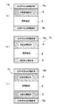
図1は実施例1における赤外線カットフィルタ1a〜1cを模式的に示した構成図である。図1(a)の赤外線カットフィルタ1aにおいて、透明基板2の表面には光吸収構造体3、近赤外光反射構造体4aが積層されている。また、透明基板2の反対の面には近赤外光反射構造体4bが成膜されている。
FIG. 1 is a configuration diagram schematically showing the
近赤外光反射構造体4a、4bは少なくとも2種類以上の無機膜を積層することにより構成されており、光吸収構造体3は色素を分散させた樹脂層により構成されている。更に、近赤外光反射構造体4a、4bは薄膜積層構造体により形成され、反射構造体4a、4bを合わせた薄膜積層構造体により、所定の波長領域の透過を制限する構成となっている。
The near-infrared
図1(b)に示す赤外線カットフィルタ1bのように、透明基板2の表面に光吸収構造体3と近赤外光反射構造体4aを積層した場合には、透明基板2の反対の面には例えば微細凹凸周期構造の反射防止構造体5を形成してもよい。或いは、単層又は複数層の薄膜より構成される反射防止膜により反射防止構造体5を形成してもよい。この反射防止構造体5には、光吸収構造体3と近赤外光反射構造体4を配置した上面との応力バランスをとる機能を持たせている。
When the
なお、図1(c)に示す赤外線カットフィルタ1cのように、透明基板2の表面側に近赤外光反射構造体4a、4bが形成される場合は、反射防止機能は近赤外光反射構造体4a、4bに含まれている場合が一般的である。
When the near-infrared
近赤外光反射構造体4a、4bの薄膜積層構造体について、紫外赤外線カットフィルタを例に挙げて以下に説明する。一般的な紫外赤外線カットフィルタは図2に示すように、可視波長領域から紫外波長領域にかけての所望する波長領域に第1阻止波長領域W1を有している。更に、可視波長領域から赤外波長領域にかけての所望する波長領域に第2阻止波長領域W2、第2阻止波長領域W2から更に赤外波長領域にかけての所望の波長領域に第3阻止波長領域W3を有する3つの阻止波長領域により構成されている。
The thin film laminated structure of the near-infrared
ここで、1つの阻止波長領域を構成する薄膜積層構造を1つのブロックとして考えると、第1〜第3阻止波長領域W1〜W3を形成する3つのブロックにより形成される。これをそれぞれ第1スタック、第2スタック、第3スタックとすると、3つのスタックのそれぞれは異なる中心波長を持っている。この波長をλとした場合に、高屈折率材料と低屈折率材料とを、それぞれ交互にλ/4ずつ積層した構成を基本とし、所望の光学特性を得るために各層の膜厚に概ね0.7〜1.3倍程度の微調を加えて積層される。 Here, when the thin film laminated structure constituting one blocking wavelength region is considered as one block, it is formed by three blocks forming the first to third blocking wavelength regions W1 to W3. If this is the first stack, the second stack, and the third stack, respectively, each of the three stacks has a different center wavelength. When this wavelength is λ, the basic structure is a structure in which high refractive index materials and low refractive index materials are alternately laminated by λ / 4, and the thickness of each layer is approximately 0 in order to obtain desired optical characteristics. Laminated with a fine adjustment of about 7 to 1.3 times.
ただし、このような構成の場合に、透明基板2や空気との界面層と、中心波長の異なる各スタック同士が隣接している層等においては、微調の範囲を超えることがあり、例えば0.5倍のλ/4程度の膜厚になることがある。更に、全層の中で上述した界面層とは別に数層、例えば全層が40層であれば1〜3層程度、微調の範囲を超える層がある場合もある。また、設計によっては中間屈折率材料を加えた3種類以上の材料により構成されることもある。
However, in the case of such a configuration, in the interface layer with the
一般に、このような多層膜は膜応力が非常に大きくなってしまうために、光学系の薄型化のために透明基板2を薄くした場合には、透明基板2の反り等に関する問題が生ずることが多い。この対策のため、積層膜を透明基板2の両面に分割して構成した場合に、理想的には透明基板2の両面に同じ材料、膜厚、膜質で積層することが最も膜応力を低減できる構成となる。しかし、この場合に膜の構成設計が困難となり、透明基板2の片面に設計した場合と同じ積層数となるように膜設計を行うと、光学特性を大きく犠牲にする可能性が高い。また、光学特性と膜応力の緩和を同時に満足するために、積層数が増加し、製作工数が増える要因となる。
In general, such a multilayer film has a very large film stress. Therefore, when the
従って、膜応力による透明基板2の反りが問題となる場合は、薄膜積層構造体を透明基板2の両面に分割し配置することが最適な手法の1つとなる。
Therefore, when the warp of the
これに加え、本実施例においては、光吸収構造体3と近赤外光反射構造体4a、4bとの応力バランスを加味することも必要となるが、それぞれの応力を予め測定しておき、透明基板2の両面への配置を最適化することで、応力バランスを取ることが必要である。この際に、所望する吸収特性を維持するために、色素の濃度の調整や、例えばスピンコート法であれば回転速度を調整する等の塗工プロセスの調整が必要となる。
In addition to this, in this embodiment, it is also necessary to consider the stress balance between the
樹脂中に分散された色素は、近赤外光反射構造体4a、4bにより形成された分光透過率の赤外光半値波長に吸収波長領域を有している。無機膜だけで形成された反射タイプの赤外線カットフィルタの場合に、半値波長でゴースト光強度の目安値が最大となる。そこで、特に撮像素子の感度が高く影響の大きい近赤外光側の半値波長、つまり透過率が50%の波長で吸収を持たせることで、反射率を50%よりも下げ、ゴースト光の強度を小さくする。
The pigment dispersed in the resin has an absorption wavelength region at the half-wavelength of infrared light of the spectral transmittance formed by the near-infrared
従って、より好ましくは、一般的に光吸収構造体3はこの赤外光半値波長を含む可視波長領域の一部である600〜750nmの間に吸収波長領域を有することが望ましい。更には、可視波長領域から近赤外波長領域に相当する400〜1200nm程度までの波長領域の中で、上述の赤外光半値波長を含む650〜800nm程度の波長領域中に、最大の吸収ピークを有することがより好ましい。
Therefore, more preferably, it is generally desirable that the
650nmよりも短い波長に吸収ピークを有する特性であると、本来必要とする透過波長領域の一部も大きく吸収してしまう可能性がある。また、800nmよりも長い波長に吸収ピークを有すると、近赤外光反射構造体4a、4bの透過波長領域から不透過波長領域への遷移波長領域で十分な吸収を得るためには複数の色素を混合する必要があり、透過波長領域でのリップルが問題となる可能性が高い。また、色素の濃度を濃くすることで対応した場合に、透過波長領域での透過率まで低下させてしまったり、光吸収構造体3を形成する樹脂層の膜厚を厚くすることで、上述したような応力が問題となる。
If the characteristic has an absorption peak at a wavelength shorter than 650 nm, there is a possibility that a part of the transmission wavelength region that is originally required may be greatly absorbed. In addition, when having an absorption peak at a wavelength longer than 800 nm, a plurality of dyes are required to obtain sufficient absorption in the transition wavelength region from the transmission wavelength region to the non-transmission wavelength region of the near-infrared
ゴースト光は強度の他に、撮像素子の感度特性や、赤外線カットフィルタ1a等の配置位置によって、その影響は様々であるが、このように概ね赤外光半値波長付近での強度を低減することで、ゴースト光による悪影響を低減することが可能である。
The influence of ghost light varies depending on the sensitivity characteristics of the image sensor and the arrangement position of the
また本実施例のように、有機膜と無機膜のハイブリッドタイプの赤外線カットフィルタ1aの場合に、有機膜による吸収と無機膜による反射を考慮し、所望の波長が赤外光半値波長となるように、予め調整することが必要となる場合がある。
Further, in the case of a hybrid type
樹脂バインダは透明基板2との屈折率差が小さいものがより好ましい。透明基板2と光吸収構造体3が隣接する場合に、屈折率差を小さくすることで、透明基板2と樹脂の界面での反射を小さくし、樹脂層の応力を低減しているので、膜厚を薄くしても、干渉効果による影響をより小さくすることが可能となる。
More preferably, the resin binder has a small refractive index difference from the
膜構成等によっても異なるが、屈折率差を概ね0.1以下にすることができれば、上述したような影響を大きく低減することが可能となる。また同様の理由から、透明基板2と光吸収構造体3との間に接着層や応力緩和層等の機能膜を挿入したような場合であっても、透明基板2、近赤外光反射構造体4、光吸収構造体3の三者の屈折率が近いものが、より望ましい。
Although it depends on the film configuration and the like, if the difference in refractive index can be reduced to about 0.1 or less, the above-described influence can be greatly reduced. For the same reason, even when a functional film such as an adhesive layer or a stress relaxation layer is inserted between the
更に、近赤外光反射構造体4a、4bの形成において、透明基板2を合成樹脂とした場合に、成膜プロセスにおける熱に起因した問題が発生する。ガラス基板と比較し、ガラス転移点が極端に低い樹脂であると、透明基板2と膜との線膨張係数の差に起因する透明基板2の反りや、反りに伴う膜面のクラックの発生等が考えられる。
Furthermore, in the formation of the near-infrared
そこで、成膜中に発生する熱への対策を講ずる必要があるが、耐熱温度の高い透明基板2の材料を選択したり、成膜を低温プロセスで行う方法が考えられる。本実施例では吸熱機構を成膜装置に持たせ、放射冷却効果により成膜中に透明基板2に発生する熱を取り除く手法を選択した。この際に、成膜プロセスで到達する透明基板2上の最高温度を予め測定し、その温度に耐えることができる透明基板2の材料を選択する必要がある。
Therefore, it is necessary to take measures against heat generated during the film formation, but a method of selecting a material for the
本実施例では、成膜プロセスの安定性を考慮し、先に実験した到達最高温度に或る程度の許容値を加味し、ガラス転移点を適性判断のパラメータとし、透明基板2には概ね70℃以上のガラス転移点を有する材料を選択した。 In this embodiment, in consideration of the stability of the film forming process, a certain allowable value is added to the highest temperature reached in the experiment, and the glass transition point is used as a parameter for determining the suitability. A material having a glass transition point of 0 ° C. or higher was selected.
また、成膜中の温度は通常の成膜に比べて特に低くなるため、何らかのアシストを付加したり、スパッタ等の比較的高エネルギで成膜し、膜密度が高くなるプロセスを選択したりすることがより好ましい。具体的には、スパッタ法、IAD法、イオンプレーティング法、IBS法、クラスタ蒸着法等の膜厚を比較的正確に制御でき、再現性の高い膜を得ることができる成膜方法であればよく、最適な方法を適宜に選択すればよい。 In addition, since the temperature during film formation is particularly low compared to normal film formation, some assistance is added, or film formation with relatively high energy, such as sputtering, is performed, and a process that increases the film density is selected. It is more preferable. Specifically, any film forming method capable of relatively accurately controlling the film thickness, such as sputtering, IAD, ion plating, IBS, and cluster deposition, and capable of obtaining a highly reproducible film. The optimal method may be selected as appropriate.
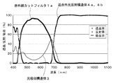
透明基板2には、厚さ0.1mmのArton(JSR製、製品名)フィルムを使用し、赤外線カットフィルタ1aは所望する紫外波長領域と赤外波長領域の一部の透過を制限した図3に示すような分光透過率特性を有するように設計をしている。
As the
Artonフィルムはガラス転移点が100℃以上あり、曲げ弾性率が約3000MPa程度と比較的高く、透明基板2の割れやうねりを低減できる理由から選択した。本実施例においては、ノルボルネン系材料であるArtonを使用したが、この他にポリイミド系の樹脂フィルム等も好適な透明基板2の1つである。また、これらに限らずPETやPEN、PES、PC等であってもよい。
The Arton film was selected because it has a glass transition point of 100 ° C. or higher and a relatively high flexural modulus of about 3000 MPa, and can reduce cracks and waviness of the
近赤外光反射構造体4aと光吸収構造体3は図1(a)に示すような配置とし、最初に光吸収構造体3を作製し、次に近赤外光反射構造体4aを作製している。
The near-infrared
光吸収構造体3は図4に示すような分光特性を有するように、シアニン系の色素をアクリル系の樹脂バインダ中に分散させ、所望の吸収を得られるように色素の濃度及び膜厚を調整し、スピンコート法により膜状に塗工し形成している。この際に、メチルエチルケトンやメチルイソブチルケトン等の溶剤を添加し、塗工後に乾燥工程を経て揮発させるのが一般的である。
The light-absorbing
また、本実施例で用いたアクリル系バインダは、透明基板2と樹脂層との密着性の観点から、スチレンを含有している樹脂材料を選択している。透明基板2の589nmの波長における屈折率は1.52程度であり、アクリル樹脂の屈折率は1.49程度であり、比較的屈折率差が小さい材料同士を組み合わせる構成としている。
In addition, the acrylic binder used in this example selects a resin material containing styrene from the viewpoint of adhesion between the
赤外線吸収色素としてシアニン系以外のアゾ系やフタロシアニン系、ナフタロシアニン系、ジイモニウム系、ポリメチン系、アンスラキノン系、ナフトキノン系、トリフェニルメタン系、アミニウム系、ピリリウム系、スクワリリウム系等の色素を用いてもよい。また、これらを2種類以上混合して用いてもよい。ただし、フィルタの色再現性を考慮すると、透過波長領域における吸収が小さく、透過波長領域における透過率が平坦又は連続的に変化することが好ましい。 Using infrared dyes such as azo dyes other than cyanine dyes, phthalocyanine dyes, naphthalocyanine dyes, diimonium dyes, polymethine dyes, anthraquinone dyes, naphthoquinone dyes, triphenylmethane dyes, aminium dyes, pyrylium dyes, squarylium dyes, etc. Also good. Moreover, you may use these in mixture of 2 or more types. However, in consideration of the color reproducibility of the filter, it is preferable that the absorption in the transmission wavelength region is small and the transmittance in the transmission wavelength region changes flatly or continuously.
また樹脂バインダとして、前述の条件を満たし、可視波長領域において透過率の高いものであれば、アクリル系、ポリスチレン系、環状オレフィン系、ポリエステル系、ポリウレタン系、フッ素系、ポリイミド系、PC(ポリカーボネート)系等の樹脂を用いてもよい。これらの樹脂を単体又は2種類以上を混合して用いてもよく、また共重合体として用いてもよい。樹脂バインダは赤外線吸収色素との相性や、透明基板2や近赤外光反射構造体4、5、紫外光反射構造体6との密着性、前後のプロセス、光学フィルタに要求される特性等を考慮しながら最適なものを適宜に選択すればよい。
If the resin binder satisfies the above conditions and has a high transmittance in the visible wavelength region, acrylic, polystyrene, cyclic olefin, polyester, polyurethane, fluorine, polyimide, PC (polycarbonate) A resin such as a resin may be used. These resins may be used alone or in combination of two or more, or may be used as a copolymer. The resin binder has compatibility with infrared absorbing dyes, adhesion to the
溶媒はケトン系に限らず、シクロヘキサン、トルエン等の炭化水素系、酢酸メチル、酢酸エチル等のエステル系、ジエチルエーテル、テトラヒドロフラン等のエーテル系、メタノール、エタノール等のアルコール系、ジメチルホルムアミド等のアミン系の溶媒や水を色素、樹脂バインダの溶解性や揮発性等を考慮し、単体又は2種類以上の混合物として最適な組合わせになるように適宜に選択すればよい。 Solvents are not limited to ketones, hydrocarbons such as cyclohexane and toluene, esters such as methyl acetate and ethyl acetate, ethers such as diethyl ether and tetrahydrofuran, alcohols such as methanol and ethanol, and amines such as dimethylformamide. In consideration of the solubility and volatility of the pigment and the resin binder, the solvent and water may be appropriately selected so as to form an optimum combination as a single substance or a mixture of two or more kinds.
また、光吸収構造体3の成膜法としてスピンコート法を選択したが、グラビア法やスプレ法等でも成膜可能であり、所望の分光を満たす膜厚や、形状、生産性等を考慮し、最適な成膜方法を選択すればよい。光吸収構造体3の成膜後に何らかの硬化工程が必要な場合には、熱硬化法に限らず、他の活性エネルギ線、例えば可視光線、電子線、プラズマ、赤外線、紫外線等を用いてもよい。活性エネルギ線の照射量は、樹脂組成物の硬化が進行するエネルギ量であればよい。
In addition, although the spin coating method is selected as the film forming method of the
また、必要に応じて光重合開始剤を添加することもできる。例えば、光重合開始剤としては、ベンゾフェノン、ベンジル、4,4−ジメチルアミノベンゾフェノン、2−クロロチオキサントン、2,4−ジエチルチオキサントン、ベンゾインエチルエーテル、ジエトキシアセトフェノン、ベンジルジメチルケタール、2−ヒドロキシ−2−メチルプロピオフェノン、1−ヒドロキシシクヘキシルフェニルケトン、テトラメチルチウラムモノスルフィド、テトラメチルチウラムジスルフィド、ヒドラゾン、α−アシロキシムエステル等が挙げられるが、これらに限定されるものでなく、単独又は複数で用いてもよい。 Moreover, a photoinitiator can also be added as needed. For example, as a photopolymerization initiator, benzophenone, benzyl, 4,4-dimethylaminobenzophenone, 2-chlorothioxanthone, 2,4-diethylthioxanthone, benzoin ethyl ether, diethoxyacetophenone, benzyldimethyl ketal, 2-hydroxy-2 -Methylpropiophenone, 1-hydroxycyclohexyl phenyl ketone, tetramethylthiuram monosulfide, tetramethylthiuram disulfide, hydrazone, α-acyloxime ester, and the like, but are not limited to these. May be used.
電子線硬化開始剤としては、例えばベンゾフェノン、2−エチルアントラキノン、2,4−ジエチルチオキサントン、メチルオルソベンゾイルベンゾエート、イソプロピルチオキサントン、ジエトキシアセトフェノン、ベンジルジメチルケタール、1−ヒドロキシシクロヘキシル−フェニルケトン、ベンゾインメチルエーテル、ベンゾインエチルエーテル、ベンゾインイソプロピルエーテル、ベンゾインイソブチルエーテル、2,4,6−トリメチルベンゾイルジフェニルホスフィンオキサイド、ビス−フェニルホスフィンオキサイド、メチルベンゾイルホルメート、1,7−ビスアクリジニルヘプタン、9−フェニルアクリジン等が挙げられるが、これらに限定されるものでなく、単独又は複数で用いることもできる。 Examples of the electron beam curing initiator include benzophenone, 2-ethylanthraquinone, 2,4-diethylthioxanthone, methyl orthobenzoylbenzoate, isopropylthioxanthone, diethoxyacetophenone, benzyldimethyl ketal, 1-hydroxycyclohexyl-phenylketone, benzoin methyl ether. , Benzoin ethyl ether, benzoin isopropyl ether, benzoin isobutyl ether, 2,4,6-trimethylbenzoyldiphenylphosphine oxide, bis-phenylphosphine oxide, methylbenzoylformate, 1,7-bisacridinylheptane, 9-phenylacridine However, the present invention is not limited to these and can be used alone or in combination.
熱重合開始剤としては、例えば過酸化ベンゾイル、t−ブチルパーベンゾエイト、クメンヒドロパーオキサイド、ジイソプロピルパーオキシジカーボネート、ジ−n−プロピルパーオキシジカーボネート、ジ(2−エトキシエチル)パーオキシジカーボネート、t−ブチルパーオキシネオデカノエート、t−ブチルパーオキシビバレート、(3,5,5−トリメチルヘキサノイル)パーオキシド、ジプロピオニルパーオキシド、ジアセチルパーオキシド、2,2−アゾビスイソブチロニトリル、2,2−アゾビス(2−メチルブチロニトリル)、1,1−アゾビス(シクロヘキサン−1−カルボニル)、2,2’−アゾビス(2,4−ジメチルバレロニトリル)、2,2−アゾビス(2,4−ジメチル−4−メトキシバレロニトリル)、ジメチル2,2−アゾビス(2−メチルプロピオネート)、4,4−アゾビス(4−シアノバレリック酸)等が挙げられるが、これらに限定されるものでなく、単独又は複数で用いてもよい。
Examples of the thermal polymerization initiator include benzoyl peroxide, t-butyl perbenzoate, cumene hydroperoxide, diisopropyl peroxydicarbonate, di-n-propyl peroxydicarbonate, and di (2-ethoxyethyl) peroxydi. Carbonate, t-butyl peroxyneodecanoate, t-butyl peroxybivalate, (3,5,5-trimethylhexanoyl) peroxide, dipropionyl peroxide, diacetyl peroxide, 2,2-azobisisobutyrate Nitrile, 2,2-azobis (2-methylbutyronitrile), 1,1-azobis (cyclohexane-1-carbonyl), 2,2′-azobis (2,4-dimethylvaleronitrile), 2,2- Azobis (2,4-dimethyl-4-methoxyvaleronitrile),
また、酸化防止剤を添加することで、色素の劣化を低減することができる場合もあり、この酸化防止剤としては、例えばフェノール系、ビンダードフェノール系、アミン系、ビンダードアミン系、硫黄系、リン酸系、亜リン酸系等が挙げられる。 In addition, by adding an antioxidant, it may be possible to reduce the deterioration of the pigment, such as phenol, binderd phenol, amine, binderd amine, sulfur , Phosphoric acid type, phosphorous acid type and the like.
近赤外光反射構造体4a、4bはIAD法により無機の誘電体膜を複数層積層体として形成している。この際に、透明基板2の反りを低減するため、この薄膜積層構造体を透明基板2の両面に分割する構成とし、先に光吸収構造体3を形成した面に反射構造体4aを形成し、その後に透明基板2の表裏を変え、反対の面に反射構造体4bを形成している。このような誘電体膜を形成する材料には、高屈折率材料にはTiO2を、低屈折率材料にはSiO2を使用し、TiO2とSiO2の交互層による構成とした。
The near-infrared
この他に、成膜手法によっても異なるが、概ね高屈折率材料としてはNb2O5やZrO2、Ta2O5等が一般的に使用され、低屈折率材用としてはMgF2が使用される場合もある。設計上や成膜上の理由から、中間屈折率材料であるAl2O3等を一部の層で使用する場合もあるが、適宜に最適な材料の組合わせを選択すればよい。 In addition, although it depends on the film forming method, generally Nb 2 O 5 , ZrO 2 , Ta 2 O 5 or the like is generally used as a high refractive index material, and MgF 2 is used for a low refractive index material. Sometimes it is done. For reasons of design and film formation, Al 2 O 3 or the like, which is an intermediate refractive index material, may be used in some layers, but an optimal combination of materials may be selected as appropriate.
透明基板2となるフィルムに誘電体膜を成膜した後に、所望の形状に打ち抜くことにより一辺が10mmの正方形状に加工する。ここで、フィルム上にマスクを施すことで、所望の範囲を部分的に成膜し、成膜後にそれぞれを切り抜くことでも、赤外線カットフィルタ1aを作製することが可能である。
After forming a dielectric film on the film to be the
簡易的な概算では、近赤外光反射構造体4a、4bのみでのゴースト光の最大強度の目安が25%であるのに対し、本実施例で作製した赤外線カットフィルタ1aの遷移波長領域でのゴースト光の最大強度の目安は8%以下となる。本実施例で作製した赤外線カットフィルタ1aでは、遷移波長領域での最大強度を3割以上も低減しており、多くの光学系でゴースト光による画像への悪影響を著しく低減させることができる。
In a simple approximation, the standard of the maximum intensity of ghost light with only the near-infrared
ここで、上述した無機膜と有機膜とのハイブリッドタイプの光学フィルタである特許文献3の実施例に記載されている構成を比較例1として、本実施例の赤外線カットフィルタ1aと比較する。
Here, the structure described in the Example of
図5(a)は特許文献4の実施例で作製された有機膜層の分光透過率、(b)は基板両面に分割し配置された2つの無機膜層1、2の分光透過率、(c)はこれらの有機膜層と無機膜層とにより作製された光学フィルタの分光透過率のグラフ図である。
5A shows the spectral transmittance of the organic film layer produced in the example of
図5(b)から無機膜層2で形成される赤外光半値波長は650nm付近の波長であることが分かる。また、(c)から有機膜層と無機膜層とにより構成した場合であっても赤外光半値波長は650nm付近であり、(b)とほぼ同様の波長となっている。
It can be seen from FIG. 5B that the half-wavelength of infrared light formed by the
図5(a)で示された有機膜層の特性から、特許文献4の有機膜層の遷移波長領域での吸収率、特に赤外光半値波長における吸収率は最大でも10%程度と非常に小さい値となっている。透過波長領域、不透過波長領域では、透過率又は反射率の何れかが0に近付くため、簡易的にはゴースト光の強度は遷移波長領域での(入射光の透過率)・(入射光の反射率)が目安となる。従って、この遷移波長領域に十分な吸収を得ることができない場合には、透過率が低いと反射率が高くなり、反射率が低いと透過率が高くなるため、ゴースト光の強度を低減することは極めて難しい。
From the characteristics of the organic film layer shown in FIG. 5 (a), the absorptance in the transition wavelength region of the organic film layer of
無機膜層のみで構成された場合には、その強度は赤外光半値波長で最大となり、透過率50%、反射率50%と仮定すると、その目安の値は25%となる。実用的にはこの強度は少なくとも15〜16%程度までは低減する必要がある。従って、実施例1において例えば強度を16%以下にまで低減するには、光吸収構造体3を組合わせて、少なくとも透過率が40%、反射率が40%となるように、遷移波長領域での光吸収構造体3の吸収率を20%以上とすることが必要である。
In the case of being composed only of an inorganic film layer, the intensity is maximum at the half-wavelength of infrared light, and assuming a transmittance of 50% and a reflectance of 50%, the standard value is 25%. Practically, this strength needs to be reduced to at least about 15 to 16%. Therefore, in Example 1, for example, in order to reduce the intensity to 16% or less, the
このように、ゴースト光は撮像素子の感度特性や、光学フィルタの配置位置等、光学系全体での構成によっても影響は微妙に異なるが、特許文献4による比較例1のような光学特性では、ゴースト光を十分に低減することは極めて困難である。
As described above, the influence of the ghost light is slightly different depending on the configuration of the entire optical system, such as the sensitivity characteristics of the image sensor and the arrangement position of the optical filter, but in the optical characteristics such as Comparative Example 1 according to
本実施例の赤外線カットフィルタ1aで高温高湿試験を実施した。赤外光半値波長のシフト量において、光学特性の変化を評価したところ、数サンプルの平均で1nm以下、最大値で1.5nmの変化が確認された。
A high-temperature and high-humidity test was conducted with the
これに対し図6に示すように、上述した赤外線カットフィルタ1aと各層の膜構成、成膜プロセス等を全く同様の構成で、近赤外光反射構造体4aと光吸収構造体3との位置を入れ換えた比較例2のサンプルを作製した。光学特性の最適化を図るための膜厚調整を行っていないため、透過波長領域で大きなリップルが発生したが、波長675nmの付近に赤外光半値波長が確認できた。
On the other hand, as shown in FIG. 6, the positions of the near-infrared
この比較例2について、同様の高温高湿試験を実施したところ、赤外光半値波長のシフト量が、数サンプルの平均で約3nm、最大値で4nmの変化が生じた。これは、有機膜の色素成分は水分に弱いため、樹脂バインダ中に色素を分散させた場合であっても、温度や湿度等の周囲環境から樹脂が少なからず吸水してしまい、光学特性が変化してしまうことがある。 When the same high-temperature and high-humidity test was carried out for Comparative Example 2, the shift amount of the half-wavelength of infrared light was changed by about 3 nm on the average of several samples and 4 nm on the maximum value. This is because the dye component of the organic film is sensitive to moisture, so even if the dye is dispersed in the resin binder, the resin absorbs water from the surrounding environment such as temperature and humidity, and the optical characteristics change. May end up.
このように、本実施例の赤外線カットフィルタ1aのような近赤外光反射構造体4aと光吸収構造体3との位置関係とすることにより、近赤外光反射構造体4aがその下の光吸収構造体3の有機膜の水分による影響を低減できることが分かる。
Thus, the near-infrared
図6に示す比較例2の光吸収構造体3の膜厚が1μmで干渉が起きないと仮定したとき、その分光透過率特性は図7(a)のグラフ中のAである。ここで光吸収構造体3の膜厚を例えば0.5μm程度まで薄くすると、干渉効果からその分光透過率特性は図7(a)のBのようになる。これに対し、光吸収構造体3の膜厚を干渉を起こさない仮定の膜厚となる2μmとしたのときの分光透過率特性は、図7(b)のCのようになる。
Assuming that no interference occurs when the film thickness of the
干渉を起こさない場合に、図7(b)のAとCを比較して分かるように、同じ材料を塗布した場合に、吸収特性は膜厚に依存するため、吸収が生ずる波長領域においては、膜厚が厚い方が吸収率は高くなる。従って、単純に吸収率の増加分だけ透過率は低下する。 In the case where no interference occurs, as can be seen by comparing A and C in FIG. 7B, when the same material is applied, the absorption characteristic depends on the film thickness. The higher the film thickness, the higher the absorption rate. Therefore, the transmittance is simply reduced by an increase in the absorption rate.
しかし、吸収がない又は少ない波長領域においては、透過率特性は殆ど変化することはない。干渉条件は光吸収構造体3の膜厚に依存しないため、初期特性以上に透過波長領域でのリップルを増大させたり、反射率が変化することで透過率を増大させる等、特性を大きく変化させたりすることはない。
However, in the wavelength region where there is no or little absorption, the transmittance characteristics hardly change. Since the interference condition does not depend on the film thickness of the
これに対し干渉が起きた場合に、図7(a)のAとBを比較すると、光吸収構造体3の膜厚によって、吸収の増減による透過の増減だけではなく、透過波長領域のリップル形状が変化しているのが分かる。これは、光吸収構造体3の膜厚によって干渉条件が変化したことから、吸収の増減分に起因した変化以外に、反射率の変化があることを示している。
On the other hand, when interference occurs, when A and B in FIG. 7A are compared, depending on the film thickness of the
図6の比較例2のように、近赤外光反射構造体4と光吸収構造体3を配置した場合には、光吸収構造体3の膜厚によっては、光学特性を大きく変化させてしまうことがあり、干渉を引き起こす程度の膜厚となった場合は、膜厚制御が極めて難しい。
When the near-infrared
図1(a)に示す実施例1のように、近赤外光反射構造体4及び光吸収構造体3を配置し、光吸収構造体3の膜厚が1μmで干渉が起きないと仮定し、その分光透過率特性が図8のAのようになった場合を説明する。特に、光吸収構造体3と透明基板2との屈折率差が0.1以下の場合に、光吸収構造体3の膜厚を例えば0.5μm程度まで薄くし干渉が起きた場合であっても、膜厚による吸収特性の差から透過特性が変化することはある。
As in Example 1 shown in FIG. 1A, it is assumed that the near-infrared
しかし、図8のBに示すように、比較例2と比べて透過波長領域に大きくリップルを発生させる等の変化は殆どない。これは透明基板2と光吸収構造体3との屈折率差が小さいため、透明基板2と近赤外光反射構造体4a、4bとの干渉効果と、光吸収構造体3と近赤外光反射構造体4a、4bとの干渉効果が略同じとなるためである。更に、透明基板2と光吸収構造体3での界面の反射が殆ど起こらないため、界面での影響にも差が殆ど生ずることはない。
However, as shown in FIG. 8B, there is almost no change such as generation of a large ripple in the transmission wavelength region as compared with Comparative Example 2. This is because the difference in refractive index between the
このような実施例1の構成であれば、干渉による光学特性の変化を小さくすることが可能であり、理想的には光吸収構造体3と透明基板2とが全く同じ屈折率であれば、透明基板2と光吸収構造体3での界面の反射がなくなる。このため、反射率の変化がなくなり、光学特性への影響は吸収率の増減による透過率の増減のみとなり、初期特性以上にリップルを発生させることはない。
With the configuration of Example 1, it is possible to reduce the change in optical characteristics due to interference. Ideally, if the
図9はビデオカメラ等の撮像装置で、レンズ11、絞り羽根12等で構成された撮像光学系13を透過した光を、光学フィルタ部14で固体撮像素子15の特性に合わせて制限し、適正な画像を得るようになっている。
FIG. 9 shows an image pickup apparatus such as a video camera. The light that has passed through the image pickup
本実施例1で作製された赤外線カットフィルタ1aを光学フィルタ部14に搭載し、このような装置に組み込み使用することにより、より高精度化を実現できる撮像装置が得られる。また、赤外線カットフィルタ1aを配置する際に、ゴースト光をより低減できるように、近赤外光反射構造体4aに対し光吸収構造体3の位置を固体撮像素子15に近くなるように配置する。
By mounting the
また、これらの赤外線カットフィルタ1aを光路内に進退自在に駆動することも可能である。より具体的には、撮像光学系13を透過して固体撮像素子15に結像した光量を判断して、固体撮像素子15の前方の光学フィルタ部14を駆動部により駆動する。入射した被写界の光量が通常の撮影に十分な量であるときは、固体撮像素子15にかかるように光学フィルタ部14を光路内に挿入し、光量が不十分なときは固体撮像素子15にかからないように光路外に退避させる。光学フィルタ部14の有無により、結像する光に光路差が発生してしまい、画像が劣化してしまうことがあるが、このような場合には赤外線カットフィルタ1aの透明基板2と同じ材質の基板をダミーとして挿入することで、画像劣化を十分に低減可能である。
It is also possible to drive these
このようにして作製された撮像装置は、ゴースト光の発生を著しく低減することができる。 The imaging device thus manufactured can significantly reduce the generation of ghost light.
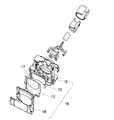
図10は光量絞り装置の構成図である。ビデオカメラ或いはデジタルスチルカメラ等の撮影系に使用する光量絞り装置16は、CCDやCMOSセンサから成る固体撮像素子15への入射光量を制御するために光路上に設けられている。被写界が明るくなるにつれ、絞り羽根12を制御し、より小さく絞り込まれてゆく構造になっている。
FIG. 10 is a block diagram of the light quantity diaphragm device. A light
このとき、小絞り状態時に発生する像性能の劣化に対する対策として、絞りの近傍にND(Neutral Density)フィルタ17を配置し、被写界の明るさが同一であっても、絞りの開口をより大きくできる構造としている。入射光がこの光量絞り装置16を通過し、固体撮像素子15に到達することで電気的な信号に変換され画像が形成される。
At this time, an ND (Neutral Density) filter 17 is disposed in the vicinity of the stop as a countermeasure against the deterioration of the image performance that occurs in the small stop state, and the aperture of the stop is further increased even if the brightness of the object field is the same. The structure can be enlarged. Incident light passes through the light
この絞り装置16内に実施例1で作製された赤外線カットフィルタ1aを配置する。赤外線カットフィルタ1aはNDフィルタ17の位置にNDフィルタに代って配置することも可能であるし、絞り羽根支持板18に固定するように配置することもできる。
The
この場合に、赤外線カットフィルタ1aを配置する位置や、絞り装置16の機械的な機構にも依存するが、赤外線カットフィルタ1aと必要な外形が異なる場合も想定される。このときは赤外線カットフィルタ1aの形状を選択すればよく、本実施例1と同様の膜設計、成膜プロセスで、成膜時に使用する打ち抜き加工機の型やマスク冶具の形状を変えることだけで、同様の赤外線カットフィルタ1aを作製することが可能である。
In this case, although it depends on the position where the
これにより作製された光量絞り装置16を撮像光学系13に配置することで、より高精度化を実現できる。この際に、実施例2と同様にゴースト光をより低減できるように、固体撮像素子に近い面側に光吸収構造体3を配置する。
By arranging the light
このようにして作製された光量調節装置は、ゴースト光の発生を著しく低減することができる。 The light quantity adjusting device thus manufactured can significantly reduce the generation of ghost light.
1a、1b、1c 赤外線カットフィルタ
2 透明基板
3 光吸収構造体
4a、4b 近赤外光反射構造体
5 反射防止構造体
12 絞り羽根
13 撮像光学系
14 光学フィルタ部
15 固体撮像素子
16 光量絞り装置
17 NDフィルタ
18 絞り羽根支持板
DESCRIPTION OF
Claims (8)
前記透明基板の一方面上に設けられ、所定の吸収波長領域を有する光吸収構造体と、
前記光吸収構造体の上に複数の無機膜を積層することによって設けられ、少なくとも近赤外波長領域の光の一部を反射する近赤外光反射構造体と、
前記透明基板の前記一方面側とは反対側の他方面の上に、複数の無機膜を積層することにより設けられ、前記近赤外反射構造体とは異なる波長領域の光の一部を反射する他の近赤外光反射構造体と、を備え、
前記光吸収構造体は、前記透明基板との屈折率差が実質的に0.1以下となるように、前記近赤外光反射構造体及び前記他の近赤外光反射構造体により形成された透過波長領域から不透過波長領域に至る遷移波長領域での分光透過率の赤外光半値波長に対応して光吸収率20%以上の光吸収波長領域を持つ色素を樹脂に分散させて、前記近赤外光反射構造体と前記透明基板との間に設けられ、前記透明基板と前記近赤外光反射構造体及び前記他の近赤外反射構造体との間の光干渉効果と、前記光吸収構造体と前記近赤外反射構造体及び前記他の近赤外光反射構造体との間の光干渉効果とを実質的に同じとしたことを特徴とする光学フィルタ。 A transparent substrate that transmits light in the visible light region;
A light absorption structure provided on one side of the transparent substrate and having a predetermined absorption wavelength region;
A near-infrared light reflecting structure that is provided by laminating a plurality of inorganic films on the light-absorbing structure, and reflects at least part of light in the near-infrared wavelength region; and
Provided by laminating a plurality of inorganic films on the other surface of the transparent substrate opposite to the one surface side, and reflects a part of light in a wavelength region different from that of the near-infrared reflective structure And other near infrared light reflecting structure,
The light absorption structure is formed by the near-infrared light reflection structure and the other near-infrared light reflection structure so that a difference in refractive index from the transparent substrate is substantially 0.1 or less. In the resin, a dye having a light absorption wavelength region of 20% or more of light absorption corresponding to the infrared half-value wavelength of the spectral transmittance in the transition wavelength region from the transmission wavelength region to the non-transmission wavelength region is dispersed, the setting between the transparent substrate and a near infrared light reflecting structure vignetting, and the optical interference effect between the transparent substrate and the near-infrared light reflecting structure and the other near-infrared reflecting structure An optical filter characterized in that the light interference effect between the light absorbing structure, the near-infrared reflecting structure, and the other near-infrared reflecting structure is substantially the same .
Priority Applications (1)
| Application Number | Priority Date | Filing Date | Title |
|---|---|---|---|
| JP2010290428A JP5789373B2 (en) | 2010-12-27 | 2010-12-27 | Optical filter |
Applications Claiming Priority (1)
| Application Number | Priority Date | Filing Date | Title |
|---|---|---|---|
| JP2010290428A JP5789373B2 (en) | 2010-12-27 | 2010-12-27 | Optical filter |
Publications (3)
| Publication Number | Publication Date |
|---|---|
| JP2012137647A JP2012137647A (en) | 2012-07-19 |
| JP2012137647A5 JP2012137647A5 (en) | 2014-09-04 |
| JP5789373B2 true JP5789373B2 (en) | 2015-10-07 |
Family
ID=46675103
Family Applications (1)
| Application Number | Title | Priority Date | Filing Date |
|---|---|---|---|
| JP2010290428A Active JP5789373B2 (en) | 2010-12-27 | 2010-12-27 | Optical filter |
Country Status (1)
| Country | Link |
|---|---|
| JP (1) | JP5789373B2 (en) |
Families Citing this family (21)
| Publication number | Priority date | Publication date | Assignee | Title |
|---|---|---|---|---|
| KR101878013B1 (en) | 2011-06-06 | 2018-08-09 | 에이지씨 가부시키가이샤 | Optical filter, solid-state imaging element, imaging device lens and imaging device |
| JP6001299B2 (en) * | 2012-03-30 | 2016-10-05 | 株式会社日本触媒 | Base material for light selective transmission filter, resin sheet, light selective transmission filter, and solid-state imaging device |
| CN102809772B (en) * | 2012-08-08 | 2015-01-07 | 晋谱(福建)光电科技有限公司 | Infrared cut-off filter with blue glass |
| WO2014104137A1 (en) * | 2012-12-28 | 2014-07-03 | 富士フイルム株式会社 | Curable resin composition, infrared cut-off filter, and solid-state imaging element using same |
| EP2940090A4 (en) * | 2012-12-28 | 2016-01-06 | Fujifilm Corp | Curable resin composition for forming infrared-reflecting film, infrared-reflecting film and manufacturing method therefor, infrared cut-off filter, and solid-state imaging element using same |
| JP6020746B2 (en) | 2013-12-26 | 2016-11-02 | 旭硝子株式会社 | Optical filter |
| CN104977642A (en) * | 2014-04-02 | 2015-10-14 | 奥普特光学有限公司 | Method for manufacturing optical filtering element |
| KR101764084B1 (en) | 2015-01-14 | 2017-08-01 | 아사히 가라스 가부시키가이샤 | Near-infrared cut filter and solid-state imaging device |
| CN106062592B (en) | 2015-01-14 | 2018-11-23 | Agc株式会社 | Near infrared ray cut-off filter and photographic device |
| JP6027154B2 (en) * | 2015-01-29 | 2016-11-16 | 京セラ株式会社 | Optical filter and optical element package |
| WO2016133099A1 (en) | 2015-02-18 | 2016-08-25 | 旭硝子株式会社 | Optical filter and imaging device |
| TW201706636A (en) * | 2015-03-31 | 2017-02-16 | Fujifilm Corp | Infrared cut-off filter and solid-state imaging element |
| TW201641459A (en) * | 2015-03-31 | 2016-12-01 | Fujifilm Corp | Infrared cut-off filter, kit, and solid-state imaging element |
| JP6202229B2 (en) | 2015-04-23 | 2017-09-27 | 旭硝子株式会社 | Optical filter and imaging device |
| KR102057256B1 (en) * | 2015-11-10 | 2019-12-18 | 주식회사 엘지화학 | Near infrared cut-off filter for the solid state image sensor |
| KR101832114B1 (en) | 2015-12-01 | 2018-02-23 | 아사히 가라스 가부시키가이샤 | Optical Filters and Imaging Devices |
| CN108603038A (en) | 2016-02-02 | 2018-09-28 | Agc株式会社 | Near infrared absorbing coloring matter, optical filter and photographic device |
| KR102465023B1 (en) * | 2016-12-27 | 2022-11-08 | 리껭테크노스 가부시키가이샤 | Laminated film with anti-reflection function and infrared shielding function |
| JP7255995B2 (en) * | 2018-10-19 | 2023-04-11 | キヤノン電子株式会社 | Optical filter and imaging device |
| WO2021131405A1 (en) * | 2019-12-23 | 2021-07-01 | Agc株式会社 | Near-infrared cut filter and imaging device |
| JP7200434B2 (en) * | 2020-02-13 | 2023-01-06 | 富士フイルム株式会社 | LAMINATED BODY, DISPLAY DEVICE AND ORGANIC ELECTROLUMINESCENT DISPLAY |
Family Cites Families (7)
| Publication number | Priority date | Publication date | Assignee | Title |
|---|---|---|---|---|
| JP4419363B2 (en) * | 2001-12-13 | 2010-02-24 | 株式会社ニコン | Imaging device provided with wavelength selection element |
| JP2004361525A (en) * | 2003-06-03 | 2004-12-24 | Dainippon Printing Co Ltd | Optical filter and display using the same |
| JP4644423B2 (en) * | 2003-09-30 | 2011-03-02 | 富士フイルム株式会社 | Color solid-state imaging device, solid-state imaging device using the color solid-state imaging device, and digital camera |
| US20070195417A1 (en) * | 2004-03-12 | 2007-08-23 | Yoshiharu Yamamoto | Light-absorbing member |
| JP2008051985A (en) * | 2006-08-24 | 2008-03-06 | Nidec Copal Corp | Near infrared ray absorbing filter |
| JP2008091535A (en) * | 2006-09-29 | 2008-04-17 | Fujifilm Corp | Solid-state imaging device |
| JP5543690B2 (en) * | 2008-03-12 | 2014-07-09 | キヤノン電子株式会社 | Optical filter for UVIR cut |
-
2010
- 2010-12-27 JP JP2010290428A patent/JP5789373B2/en active Active
Also Published As
| Publication number | Publication date |
|---|---|
| JP2012137647A (en) | 2012-07-19 |
Similar Documents
| Publication | Publication Date | Title |
|---|---|---|
| JP5789373B2 (en) | Optical filter | |
| JP5823119B2 (en) | Optical filter for UV-IR cut | |
| JP5693949B2 (en) | Optical filter | |
| JP5819063B2 (en) | Optical filter | |
| WO2012157719A1 (en) | Optical filter and optical device | |
| JP5759717B2 (en) | Imaging optical system for surveillance cameras | |
| JP2012137649A (en) | Optical filter | |
| JP4900678B2 (en) | Aperture device having ND filter and optical apparatus | |
| JP2012137651A (en) | Optical filter | |
| JP2008058438A (en) | Optical filter | |
| CN110873914A (en) | Optical filter, method for manufacturing the same, solid-state imaging device, and camera module | |
| JP2007178822A (en) | Light quantity control nd filter | |
| WO2012023372A1 (en) | Optical functional element and imaging device | |
| JP2010175941A (en) | Optical filter and method of manufacturing the same, and image capturing apparatus having the same | |
| JP4671410B2 (en) | Light aperture device and camera with ND filter with IR cut function | |
| JP6595220B2 (en) | Optical filter and camera equipped with optical filter | |
| JP2017003842A (en) | Optical filter, light intensity adjustment device having optical filter mounted therein, and imaging optical system | |
| JP2011101089A (en) | Imaging optical system and imaging apparatus | |
| JP2013033241A (en) | Optical filter, optical device and method for manufacturing optical filter | |
| JP5478203B2 (en) | Imaging device | |
| JP2016071278A (en) | Optical filter and light quantity adjusting device, and imaging apparatus | |
| JP5942472B2 (en) | Light intensity adjustment device | |
| JP7251423B2 (en) | Optical components and camera modules | |
| JP2007316238A (en) | Nd filter | |
| US10158791B2 (en) | Camera device with red halo reduction |
Legal Events
| Date | Code | Title | Description |
|---|---|---|---|
| A621 | Written request for application examination |
Free format text: JAPANESE INTERMEDIATE CODE: A621 Effective date: 20131227 |
|
| A521 | Request for written amendment filed |
Free format text: JAPANESE INTERMEDIATE CODE: A821 Effective date: 20140714 Free format text: JAPANESE INTERMEDIATE CODE: A523 Effective date: 20140714 |
|
| RD02 | Notification of acceptance of power of attorney |
Free format text: JAPANESE INTERMEDIATE CODE: A7422 Effective date: 20140714 |
|
| A977 | Report on retrieval |
Free format text: JAPANESE INTERMEDIATE CODE: A971007 Effective date: 20140903 |
|
| A131 | Notification of reasons for refusal |
Free format text: JAPANESE INTERMEDIATE CODE: A131 Effective date: 20140916 |
|
| A521 | Request for written amendment filed |
Free format text: JAPANESE INTERMEDIATE CODE: A821 Effective date: 20141117 Free format text: JAPANESE INTERMEDIATE CODE: A523 Effective date: 20141117 |
|
| A02 | Decision of refusal |
Free format text: JAPANESE INTERMEDIATE CODE: A02 Effective date: 20150106 |
|
| A521 | Request for written amendment filed |
Free format text: JAPANESE INTERMEDIATE CODE: A523 Effective date: 20150403 Free format text: JAPANESE INTERMEDIATE CODE: A821 Effective date: 20150403 |
|
| A911 | Transfer to examiner for re-examination before appeal (zenchi) |
Free format text: JAPANESE INTERMEDIATE CODE: A911 Effective date: 20150410 |
|
| TRDD | Decision of grant or rejection written | ||
| A01 | Written decision to grant a patent or to grant a registration (utility model) |
Free format text: JAPANESE INTERMEDIATE CODE: A01 Effective date: 20150707 |
|
| A61 | First payment of annual fees (during grant procedure) |
Free format text: JAPANESE INTERMEDIATE CODE: A61 Effective date: 20150803 |
|
| R150 | Certificate of patent or registration of utility model |
Ref document number: 5789373 Country of ref document: JP Free format text: JAPANESE INTERMEDIATE CODE: R150 |
|
| R250 | Receipt of annual fees |
Free format text: JAPANESE INTERMEDIATE CODE: R250 |
|
| R250 | Receipt of annual fees |
Free format text: JAPANESE INTERMEDIATE CODE: R250 |
|
| R250 | Receipt of annual fees |
Free format text: JAPANESE INTERMEDIATE CODE: R250 |
|
| R250 | Receipt of annual fees |
Free format text: JAPANESE INTERMEDIATE CODE: R250 |
|
| R250 | Receipt of annual fees |
Free format text: JAPANESE INTERMEDIATE CODE: R250 |
|
| R250 | Receipt of annual fees |
Free format text: JAPANESE INTERMEDIATE CODE: R250 |
|
| R250 | Receipt of annual fees |
Free format text: JAPANESE INTERMEDIATE CODE: R250 |