JP6556529B2 - Optical filter and optical device provided with optical filter - Google Patents
Optical filter and optical device provided with optical filter Download PDFInfo
- Publication number
- JP6556529B2 JP6556529B2 JP2015133961A JP2015133961A JP6556529B2 JP 6556529 B2 JP6556529 B2 JP 6556529B2 JP 2015133961 A JP2015133961 A JP 2015133961A JP 2015133961 A JP2015133961 A JP 2015133961A JP 6556529 B2 JP6556529 B2 JP 6556529B2
- Authority
- JP
- Japan
- Prior art keywords
- film
- filter
- optical
- light
- fine structure
- Prior art date
- Legal status (The legal status is an assumption and is not a legal conclusion. Google has not performed a legal analysis and makes no representation as to the accuracy of the status listed.)
- Active
Links
Images


Description
本発明は、反射低減機能を発現する微細構造を備えた光学フィルタ、及びこの光学フィルタを備えた光学装置に関する。 The present invention relates to an optical filter having a fine structure that exhibits a reflection reducing function, and an optical device including the optical filter.
光量絞りは銀塩フィルム、或いはCCDやCMOSセンサと言った固体撮像素子への入射光量を制御するために設けられているものであり、被写界が明るくなるにつれ、より小さく絞り込まれていく構造になっている。したがって、快晴時や高輝度の被写界を撮影する際、絞りはいわゆる小絞り状態となり、光の回折現象などの影響を受け易いことから、像性能に劣化を生じさせる場合がある。 The aperture stop is provided to control the amount of incident light on a solid-state image sensor such as a silver salt film or a CCD or CMOS sensor, and the aperture is further reduced as the field becomes brighter. It has become. Therefore, when photographing a clear or high-brightness scene, the diaphragm is in a so-called small-aperture state, and is susceptible to the effects of light diffraction and the like, which may degrade image performance.
これに対する対策として、絞りの近傍にND( N e u t r a l D e n s i t y)フィルタを配置することで光量の制御を行い、被写界の明るさが同一であっても、絞りの開口をより大きくできる様な工夫をしている。 As a countermeasure against this, even if the brightness of the object field is the same, the amount of light is controlled by disposing an ND (Neutral Density) filter in the vicinity of the stop. The device is designed to make the aperture opening larger.
近年では撮像素子の感度が向上するに従い、NDフィルタの濃度を濃くして、光の透過率をさらに低下させ、高感度の撮像素子を使用した場合であっても、絞りの開口が小さくなり過ぎないようにする改善がなされてきた。しかし、NDフィルタの濃度が濃くなると、例えばNDフィルタを通過した光束と通過しない光束との光量差や、高濃度領域を通過した光束と低濃度領域を通過した光束との光量差などが大きく異なることに起因して、画像が劣化する不具合が発生する場合がある。この問題を解決するために、NDフィルタの濃度を連続的に変化させる構成とした、グラデーション濃度勾配を有するNDフィルタ(以下、グラデーションNDフィルタ)が必要とされている。ここで、濃度Dとは、透過率TからD=log10(1/T)で求めた値である。 In recent years, as the sensitivity of the image sensor increases, the density of the ND filter is increased to further reduce the light transmittance, and even when a highly sensitive image sensor is used, the aperture of the diaphragm becomes too small. Improvements have been made to prevent it. However, when the density of the ND filter is high, for example, the difference in the amount of light between the light beam that has passed through the ND filter and the light beam that has not passed through, or the difference in light amount between the light beam that has passed through the high density region and the light beam that has passed through the low density region is significantly different. As a result, there may be a problem that the image deteriorates. In order to solve this problem, there is a need for an ND filter having a gradation density gradient (hereinafter referred to as gradation ND filter) having a configuration in which the density of the ND filter is continuously changed. Here, the density D is a value obtained from the transmittance T by D = log 10 (1 / T).
撮像光学系などで使用される、このようなNDフィルタでは、フィルタを透過した光の一部が、他の部材によって反射され、フィルタの光出射面から、再びフィルタに入射される現象が起きる場合がある。このような場合に、NDフィルタがこの入射光の波長領域に反射を持っていると、フィルタで入射光を再度反射してしまい、画像劣化など、これに起因した不具合を発生させることがある。従って、NDフィルタにおける反射防止機能の更なる強化が強く望まれている。 In such an ND filter used in an imaging optical system or the like, a phenomenon occurs in which a part of light transmitted through the filter is reflected by another member and is incident on the filter again from the light emission surface of the filter. There is. In such a case, if the ND filter has a reflection in the wavelength region of the incident light, the incident light is reflected again by the filter, which may cause problems such as image degradation. Therefore, further enhancement of the antireflection function in the ND filter is strongly desired.
さらに、膜厚を連続的に変化させることで連続的に濃度を変化させたグラデーションNDフィルタであっても、撮像素子などの高精度化に伴い、同一フィルタ内の各濃度において積層された膜厚の違いから、位相差が発生し画像が劣化してしまう不具合が生じることがある。 Furthermore, even with a gradation ND filter in which the density is continuously changed by continuously changing the film thickness, the film thickness laminated at each density in the same filter as the accuracy of the image sensor and the like increases. Due to this difference, there may be a problem that a phase difference occurs and the image deteriorates.
このような反射に対する対策として、特許文献1には、NDフィルタに可視光の波長サイズ以下のピッチで構成された微細構造体を用いることで、光学フィルタの反射率を低減する方法が、特許文献2、及び特許文献3には、NDフィルタにおける前述の位相差を低減する方法がそれぞれ開示されている。 As a countermeasure against such reflection, Patent Document 1 discloses a method for reducing the reflectance of an optical filter by using a fine structure having a pitch equal to or smaller than the wavelength size of visible light for an ND filter. 2 and Patent Document 3 disclose methods for reducing the above-described phase difference in the ND filter.
特許文献1で示されているような反射低減効果を持つ微細構造体は、真空成膜法などで薄膜を単層、または複数層を積層することにより作製する反射防止膜と比較し、低反射率を容易に実現でき、更には反射防止波長領域を拡げることなどが比較的容易で、入射角度による分光反射率の相違が小さいと言った様々なメリットを有しており、屈折率の変化を緩やかにすることで、より反射を低減させることが可能である。 The fine structure having a reflection reducing effect as shown in Patent Document 1 has a low reflection compared with an antireflection film produced by stacking a single thin film or a plurality of layers by a vacuum film formation method or the like. The ratio can be easily realized, and it is relatively easy to expand the antireflection wavelength region, etc., and it has various advantages such as a small difference in spectral reflectance depending on the incident angle. By making it gentle, reflection can be further reduced.
また特許文献2では、透明部を備えたNDフィルタの開口に、フィルタ端部を露出させないように構成・制御することで、NDフィルタを透過する光と、NDフィルタを透過せずに進む光との位相差を低減させることで画像の劣化等を抑制する方法が提案されている。 Moreover, in patent document 2, the light which permeate | transmits a ND filter and the light which does not permeate | transmit a ND filter by comprising and controlling so that a filter edge part may not be exposed to the opening of a ND filter provided with the transparent part. There has been proposed a method for suppressing image degradation and the like by reducing the phase difference between the two.
しかしながら、特許文献2で開示されている方法では、膜厚を連続に変化させ形成したグラデーションNDフィルタの、濃度勾配領域における膜厚差に起因した位相差までを低減することは難しい。さらには、特許文献1、2に開示されているそれぞれの対策だけでは、グラデーションNDフィルタの濃度勾配領域における反射低減と位相差低減を同時に実現することはできず、さらには特許文献1、2の構成を組合せて、これを実現することも大変難しい。 However, with the method disclosed in Patent Document 2, it is difficult to reduce the phase difference caused by the film thickness difference in the density gradient region of the gradation ND filter formed by continuously changing the film thickness. Furthermore, it is not possible to simultaneously achieve reflection reduction and phase difference reduction in the density gradient region of the gradation ND filter with only the countermeasures disclosed in Patent Documents 1 and 2, and It is also very difficult to achieve this by combining the configurations.
そこで本筆者らは特許文献3において、膜厚を連続的に変化させ形成したグラデーションNDフィルタの、濃度勾配領域が配置された領域に対峙した基板の裏面側に、濃度勾配領域の膜厚分布と逆テーパ状の膜厚分布を持つ多層膜構造の反射防止膜を形成する方法を提案した。当時の技術では、これらの方法でも十分な反射低減効果を得て、膜厚差に起因した位相差を低減することが可能であったが、近年の高精度化の要求に応える為には、位相差を低減しつつ更なる反射の低減を図ることが必要とされている。 Therefore, in Patent Document 3, the authors have disclosed the film thickness distribution of the concentration gradient region on the back side of the substrate facing the region where the concentration gradient region is arranged in the gradation ND filter formed by continuously changing the film thickness. A method of forming an antireflection film having a multilayered film structure with an inversely tapered film thickness distribution was proposed. With the technology at that time, it was possible to obtain a sufficient reflection reduction effect even with these methods and reduce the phase difference due to the film thickness difference, but in order to meet the recent demand for higher accuracy, There is a need to further reduce reflection while reducing the phase difference.
また、段階的な濃度変化を有する多濃度タイプのNDフィルタや、透明領域を有するIRカットフィルタなど、複数の膜厚領域を有する他の光学フィルタにおいても、同様に複数の膜厚領域全域における反射と位相差を低減することが望まれている。 Similarly, in other optical filters having a plurality of film thickness regions, such as a multi-concentration type ND filter having a stepwise density change and an IR cut filter having a transparent region, reflection in the entire region of the plurality of film thickness regions is similarly performed. It is desired to reduce the phase difference.
本発明は、入射光に対する反射を低減しつつ位相差を低減する光学フィルタ及び光学装置を提供する。 The present invention provides an optical filter and an optical device that reduce phase difference while reducing reflection with respect to incident light.
本発明の光学フィルタは、可視波長領域の光を透過する透明基板と、前記透明基板上に設けられた機能膜と、を備え、前記機能膜は、前記透明基板の上に設けられた膜厚が異なる複数の領域が形成された光学膜と、前記光学膜の上に設けられた光の波長サイズよりも短いピッチで複数の微細構造が形成された微細構造体と、を有し、前記微細構造体は、前記微細構造の形状を前記複数の領域でそれぞれ異なる形状としたことを特徴とする。
また、本発明の光学フィルタは、可視波長領域の光を透過する透明基板と、前記透明基板上に設けられた機能膜と、を備え、前記機能膜は、前記透明基板上に設けられた膜厚が異なる複数の領域が形成された光学膜と、前記光学膜上に設けられた光の波長サイズよりも短いピッチで複数の微細構造から形成された微細構造体と、を有し、前記微細構造体は、前記光学膜の膜厚変化に応じて異なる形状の微細構造を有することを特徴とする。
The optical filter of the present invention includes a transparent substrate that transmits light in a visible wavelength region, and a functional film provided on the transparent substrate, and the functional film is a film thickness provided on the transparent substrate. An optical film in which a plurality of regions differing from each other and a fine structure in which a plurality of fine structures are formed at a pitch shorter than the wavelength size of light provided on the optical film, The structure is characterized in that the microstructure has a different shape in each of the plurality of regions.
The optical filter of the present invention includes a transparent substrate that transmits light in the visible wavelength region, and a functional film provided on the transparent substrate, and the functional film is a film provided on the transparent substrate. An optical film in which a plurality of regions having different thicknesses are formed, and a fine structure formed from a plurality of fine structures at a pitch shorter than the wavelength size of light provided on the optical film, The structure has a microstructure having a different shape according to a change in the thickness of the optical film.
本発明によれば、膜厚を連続的に変化させ形成したグラデーションNDフィルタなど、基板上に複数の膜厚領域を持つ光学フィルタにおいて、それぞれの領域の膜厚に合わせて位相差を低減するように構造形状を調整した、反射低減効果の高い微細構造体を配置することで、十分な反射低減効果を得つつ、位相差を低減することができる。さらには、このような光学フィルタを搭載することで、画像劣化などの不具合を改善した、高精度化を実現できる光学装置を得ることができる。 According to the present invention, in an optical filter having a plurality of film thickness regions on a substrate, such as a gradation ND filter formed by continuously changing the film thickness, the phase difference is reduced in accordance with the film thickness of each region. By disposing a fine structure having a high reflection reduction effect with the structural shape adjusted, it is possible to reduce the phase difference while obtaining a sufficient reflection reduction effect. Furthermore, by mounting such an optical filter, it is possible to obtain an optical device that can improve the accuracy and improve defects such as image degradation.
本発明に係る微細構造体は、例えば、図1に示したような、基板上に形成された、光の波長サイズよりも短いピッチで配置された、反射低減効果を有する無数の微細構造により構成される。また、本発明に係る光学フィルタは、前述の基板と微細構造体に加え、所定の光学特性を発現する光学膜を有している。 The fine structure according to the present invention is constituted by an infinite number of fine structures having a reflection reducing effect, which are arranged on a substrate, for example, as shown in FIG. 1 and arranged at a pitch shorter than the wavelength size of light. Is done. The optical filter according to the present invention includes an optical film that exhibits predetermined optical characteristics in addition to the above-described substrate and microstructure.
微細構造体や光学膜を形成する為の基板としては、微細構造体や光学膜の基板としての強度や光学特性を有するものであれば良く、基体として機能可能であるものが利用される。このような基板としては、BK7やSFL−6などガラス系の材料からなる基板、またはPET(ポリエチレンテレフタレート)、PEN(ポリエチレンナフタレート)、PES(ポリエーテルサルホン)、PC(ポリカーボネート)、PO(ポリオレフィン)、PI(ポリイミド)、PMMA(ポリメチルメタクリレート)、及びTAC(トリアセチルセルロース)等から選択した樹脂材料からなる基板を用いることができる。また、ガラス基板と樹脂層との複合材料からなる基板や、有機材と無機材を混合させた有機無機ハイブリッド基板などを用いることもできる。 The substrate for forming the microstructure or the optical film may be any substrate having the strength and optical characteristics of the microstructure or the optical film as the substrate, and a substrate that can function as a substrate is used. As such a substrate, a substrate made of a glass-based material such as BK7 or SFL-6, or PET (polyethylene terephthalate), PEN (polyethylene naphthalate), PES (polyethersulfone), PC (polycarbonate), PO ( A substrate made of a resin material selected from polyolefin, PI (polyimide), PMMA (polymethylmethacrylate), TAC (triacetylcellulose), and the like can be used. A substrate made of a composite material of a glass substrate and a resin layer, an organic-inorganic hybrid substrate in which an organic material and an inorganic material are mixed, and the like can also be used.
以上のような基板上に、複数の異なる膜厚領域を持つ、例えば膜厚を変化させることで濃度を変化させた濃度勾配領域を有する、多層薄膜で構成されたグラデーションタイプのND膜などを形成する。このようなND膜には、基板中に光を吸収する有機色素または顔料を混ぜて練り込むタイプのものや、これらを塗布するタイプのものなどがあるが、このような方式では分光透過率の波長依存性が大き過ぎると言った致命的な欠点がある。したがって、蒸着法やスパッタ法など真空成膜法や、ゾルゲル法などの成膜方法により、プラスチックやガラスなどの透明基板上に、多層膜を形成する構成とし、濃度勾配領域は吸収層を含む多層膜全体の膜厚を連続的に変化させる構成とした。また、透明領域を有するIRカット膜やUVカット膜のように、ND膜以外の光学膜でも良く、これらの光学膜も蒸着法やスパッタ法など真空成膜法や、ゾルゲル法などの成膜方法により、プラスチックやガラスなどの透明基板上に、多層膜を形成する構成とした。 On the substrate as described above, a gradation type ND film having a plurality of different film thickness regions, for example, having a concentration gradient region in which the concentration is changed by changing the film thickness, and formed of a multilayer thin film is formed. To do. Such ND films include a type in which organic dyes or pigments that absorb light are mixed into a substrate and kneaded, and a type in which these are applied. There is a fatal defect that the wavelength dependence is too large. Therefore, a multilayer film is formed on a transparent substrate such as plastic or glass by a vacuum film formation method such as an evaporation method or a sputtering method, or a film formation method such as a sol-gel method, and the concentration gradient region is a multilayer including an absorption layer. It was set as the structure which changes the film thickness of the whole film | membrane continuously. Further, an optical film other than the ND film, such as an IR cut film or a UV cut film having a transparent region, may be used. These optical films may also be formed by a vacuum film formation method such as an evaporation method or a sputtering method, or a film formation method such as a sol-gel method. Thus, a multilayer film is formed on a transparent substrate such as plastic or glass.
以上のようなND膜などの光学膜上に反射低減効果を発現する微細構造体を形成し、これら光学膜と微細構造体とを組み合わせた機能膜を透明基板上に形成する。光がある物質に入射すると、入射する前後の物質の屈折率差に起因して、物質表面でフレネル反射と呼ばれる反射が起こる。このような反射は、物質間の屈折率差を小さくすることで低減することが可能である。この屈折率差を低減する方法の1つとして、物質の構造体形状を利用する方法が各種提案されている。微細構造体は、近年の微細加工技術の向上とともに作製されるようになってきており、モス・アイに代表される凹凸構造を持つこれらの微細構造は、2つの物質間で構造体形状を連続的に変化させることで、物質間の屈折率を連続的に変化させ、反射の低減を図ったものである。本発明における微細構造体は、特には反射低減機能を有する前述のような構造体であり、可視光の波長よりも短いピッチで配列された凹凸形状を有したものである。このような微細構造の1種として、ランダムに形成された針状体及び柱状体等の突起、階段形状に微細に形成された凹凸構造の突出部または凹部によって、大気や隣接する媒体との屈折率差を低減したものが含まれても良く、公知の微細構造から目的に応じて任意に選択したものを用いることができる。 A fine structure that exhibits a reflection reduction effect is formed on the optical film such as the ND film as described above, and a functional film in which the optical film and the fine structure are combined is formed on the transparent substrate. When light is incident on a material, reflection called Fresnel reflection occurs on the surface of the material due to the difference in refractive index between the materials before and after the incidence. Such reflection can be reduced by reducing the difference in refractive index between materials. As one method for reducing this difference in refractive index, various methods using the structure of a substance have been proposed. Microstructures are being manufactured with recent improvements in microfabrication technology, and these microstructures with a concavo-convex structure typified by moth-eye have a continuous structure shape between two substances. In this way, the refractive index between substances is continuously changed to reduce reflection. The fine structure in the present invention is the above-described structure having a reflection reducing function, and has a concavo-convex shape arranged at a pitch shorter than the wavelength of visible light. As one type of such a fine structure, refraction from the atmosphere or an adjacent medium is caused by randomly formed protrusions such as needle-like bodies and columnar bodies, and protrusions or depressions of a concavo-convex structure finely formed in a staircase shape. What reduced the rate difference may be included, and what was arbitrarily selected according to the objective from the well-known fine structure can be used.
このような微細構造体であれば、熱ナノインプリント法や、光ナノインプリント法などの方法を用いて再現性良く作製することができる。 Such a fine structure can be manufactured with good reproducibility using a method such as a thermal nanoimprint method or an optical nanoimprint method.
さらに、本発明による構成の場合、微細構造体と光学膜を形成する多層膜の最表層や、微細構造体と基板との間などに界面が形成されるが、反射低減効果を有する微細構造体を形成する場合、光学フィルタ総体としての反射を低減する為には、これら異なる物質間での界面反射も低減する必要がある。従って、界面を形成する2つの物質間の屈折率差はできるだけ小さくすることが望ましい。 Furthermore, in the case of the configuration according to the present invention, an interface is formed on the outermost layer of the multilayer film that forms the microstructure and the optical film, or between the microstructure and the substrate, but the microstructure has an effect of reducing reflection. In order to reduce the reflection as a whole of the optical filter, it is necessary to reduce the interface reflection between these different substances. Therefore, it is desirable to make the difference in refractive index between the two substances forming the interface as small as possible.
以下、本発明の光学フィルタ、及び光学装置について、実施例に基づき具体的に説明する。 Hereinafter, the optical filter and the optical device of the present invention will be specifically described based on examples.
(実施例1)
透明基板上に多層薄膜で構成された濃度勾配領域を有するグラデーションタイプのND膜を形成し、更にND膜の直上となる、NDフィルタの最表層部に微細構造体を形成した実施例について、以下に詳しく記載する。
Example 1
Regarding an embodiment in which a gradation type ND film having a concentration gradient region composed of a multilayer thin film is formed on a transparent substrate, and a fine structure is formed on the outermost layer portion of the ND filter, which is directly above the ND film. Is described in detail.
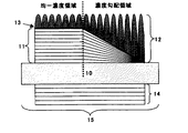
最初に、図2に示す構成において、厚さ1.0mmのBK−7ガラスを基板10として、この基板10の片面側に、膜厚が一定の均一濃度領域と、膜厚が連続的に変化している濃度勾配領域とを有する、多層薄膜で構成されたグラデーションND膜11を、特にアシストを付加しない通常のEB蒸着法により形成した後、基板の表裏を反転させ、基板上のもう一方の面上に、同様の通常のEB蒸着法により多層薄膜で構成された反射防止膜14を作製した。このような真空蒸着法は、膜厚を比較的に容易に制御でき、かつ可視光波長領域において散乱が非常に小さく、分光透過率の波長依存性を小さい値に制御することが可能な利点を有している。ただし、成膜方法はEB蒸着法に限定されず、スパッタリング法、IAD法、IBS法、イオンプレーティング法、クラスタ蒸着法等の成膜方法においても成膜が可能であるし、ゾルゲル法などのウエット系の成膜方法でも良く、目的や条件等を考慮し、最も適当な成膜方法を選択すればよい。また、本実施例のような光学フィルタであるNDフィルタ15に用いる基板10の光学特性としては、可視光波長領域における全光線透過率89%以上が好ましく、91%以上がさらに好ましい。
First, in the configuration shown in FIG. 2, a BK-7 glass having a thickness of 1.0 mm is used as the
グラデーションND膜11を構成する薄膜材料として、SiO2やAl2O3などの誘電体層と、Ti、Nb、Ta、Zr、Ni、Cr、W、Mo、Au、Ag、Cu、Mg、Alなどの金属単体、またはこれらの合金や金属化合物により構成された光吸収層に加え、最表層には特に反射低減を目的として、比較的屈折率が低いMgF2やSiO2などを用いることが可能であるが、本実施例では図4(a)で示すような積層構造とし、最表層はSiO2層とした。しかし、これに限らず、先に挙げたMgF2に加え、例えばAl2O3や、SiOなど酸価を変えたもの、SiNなど、SiやAl、Mgの金属化合物や、これらを混合させた層などを適宜選択することが可能である。同様にTi、Nb、Ta、Zr、Ni、Cr、W、Mo、Au、Ag、Cuなどの金属化合物であっても良い。また、反射防止膜14も同様に様々な薄膜材料を用いることができ、本実施例1では図4(b)で示すように、最表層をSiO2とし、SiO2とTiO2を交互に5層積層した構成としたが、これに限らず適宜選択することが可能である。
As a thin film material constituting the gradation ND film 11, a dielectric layer such as SiO 2 or Al 2 O 3 and Ti, Nb, Ta, Zr, Ni, Cr, W, Mo, Au, Ag, Cu, Mg, Al In addition to light absorption layers composed of simple metals such as these, or alloys and metal compounds thereof, it is possible to use MgF 2 or SiO 2 with a relatively low refractive index for the purpose of reducing reflection particularly for the outermost layer. However, in this example, a laminated structure as shown in FIG. 4A was used, and the outermost layer was an SiO 2 layer. However, the present invention is not limited to this, and in addition to the MgF 2 listed above, for example, Al 2 O 3 , a material with a changed acid value such as SiO, SiN or the like, a metal compound of Si, Al, or Mg, or a mixture thereof. A layer or the like can be appropriately selected. Similarly, metal compounds such as Ti, Nb, Ta, Zr, Ni, Cr, W, Mo, Au, Ag, and Cu may be used. Similarly, various thin film materials can be used for the
ここで、このようなグラデーションND膜11の膜構成において、本実施例では、ND膜11の最表層となるSiO2層と、その上に形成される密着層や微細構造体などの物質との界面での反射を無視し、それ以外の界面での反射を光干渉効果により相殺させることで、それ以外の界面での総体的な反射を可能な限り小さくする膜構成とした。これは以下の理由からである。 Here, in such a film configuration of the gradation ND film 11, in this embodiment, the SiO 2 layer which is the outermost layer of the ND film 11, and substances such as an adhesion layer and a fine structure formed thereon are formed. Reflection at the interface was ignored, and reflection at the other interface was canceled by the light interference effect, so that the total reflection at the other interface was made as small as possible. This is for the following reason.
例えば、グラデーションND膜11上に直接微細構造体12を形成する場合を考える。まず、グラデーションND膜11の最表層と微細構造体12との屈折率差を小さくすることで、この界面での反射を可能な限り低減し、微細構造体の反射低減効果を利用することで、媒質(空気)からグラデーションND膜11の最表層までの反射を理想的に低減する。次に、グラデーションND膜11における基板10側に向かう最表層以降では、最表層のSiO2と微細構造体12との界面以外の界面の光干渉効果により反射を低減する。そして、これら2つの反射低減構成を組合せることにより、NDフィルタ15総体としての反射を低減させる。筆者らは、多層構成の光学膜で形成される光学フィルタにおいて、全ての界面の中で、最表層と、空気などの最表層との屈折率差が大きい入射媒質との界面での反射が、光学フィルタとしての反射に与える影響が最も大きく、この部分の反射を十分に低減し、さらに他の全ての界面の反射を相殺させる構成とすることで、光干渉効果により形成される反射を低減すれば、光学フィルタとしての総体的な反射をより小さくできることを見出した。従って、このような構成であれば、NDフィルタ15の反射を著しく低減させることが可能となる。ここでは、グラデーションND膜11直上に微細構造体12を形成する場合を例に説明したが、グラデーションND膜11上に密着層13を介し、微細構造体12を形成した場合も同様のコンセプトで設計することが可能である。この場合、例えばグラデーションND膜11と密着層13との界面反射を小さくすると共に、密着層13と微細構造体12との界面反射を小さくし、微細構造体の反射低減効果を利用する構成とすれば良い。さらに別の方法として、密着層13をグラデーションND膜11の最表層と考え、前述と同様のコンセプトでグラデーションND膜11の多層膜構成を決定した後、グラデーションND膜11の最表層とした密着層11と、微細構造体12との屈折率差を小さくすることで、この界面での反射を低減し、NDフィルタ15総体の反射を低減することも可能である。
For example, consider a case where the
以上のように作製されたグラデーションND膜11上に密着層13を介し微細構造体12を形成した。微細構造体に関しては様々な作製方法が提案されているが、本実施例ではUV(紫外線)硬化樹脂を用いた光ナノインプリント法を選択した。
A
まず、グラデーションND膜11の最表層と微細構造体12との密着性を向上させる為に、プライマー処理を行い、これらの界面に密着層13を設けた。このようなプライマー溶液の例としては、シランカップリング剤をベースに、IPAや硝酸等を適量加え、さらに密着力を強化する目的で、TEOSを加えたものを用いた。これを、0.2μmのPTFE(ポリテトラフルオロエチレン)フィルタを介し基板上に滴下し、スピンコートにより極薄膜となるように塗工した後、所定の条件で乾燥処理等を行い、密着層13を形成する。さらに、基板10やグラデーションND膜11など他の層に何らかの悪影響を与えない範囲であれば、プライマー液をより均一に塗工する為に、プライマー液塗工前に、UVオゾンなどによる親水化処理を施しても良い。また、このようなプロセスによる塗工を行う際、マスキングを施したり、成膜プロセスをインクジェット法やグラビア法、マイクロコンタクトプリント法などに変えたりすることで、塗工領域を制限することも可能である。
First, in order to improve the adhesion between the outermost layer of the gradation ND film 11 and the
この際、前述のように、より高い反射低減効果を必要とする場合は、隣接する界面での屈折率差は0.1以下に調整されることが好ましく、0.05以下が更に望ましい。本実施例1においては、密着層13の波長540nmでの屈折率は1.47となるように調整しており、グラデーションND膜11との界面層となる、グラデーションND膜11の最表層SiO2の屈折率は1.46、微細構造体12の屈折率は1.51であるから、それぞれの界面での屈折率差を、0.01、0.04とするように構成した。
At this time, as described above, when a higher reflection reduction effect is required, the refractive index difference at the adjacent interface is preferably adjusted to 0.1 or less, and more preferably 0.05 or less. In Example 1, the refractive index at a wavelength of 540 nm of the
次に、本実施例1における微細構造体12は、図1で示したような突起構造を周期的に配置したピラーアレイ状とし、構造体は釣鐘型のモス・アイ形状で構造体の周期は約250nmとした。さらに、突起構造体の配列に関して、正方配列や三方(六方)配列などが考えられるが、三方配列の方が基板材料の露出面が少ないことなどから、反射低減効果が高いとされており、この理由から本実施例では三方配列とした。
Next, the
また、図2で示すように、均一濃度領域では微細構造体12は略同じ構造高さであるが、濃度勾配領域ではグラデーションND膜11の膜厚が薄いほど構造高さが高くなるように構成した。これは、グラデーションND膜11の膜厚差に起因した位相差を低減する目的であり、構造体の屈折率や、グラデーションND膜11の構成材料によっても、最適な微細構造高さは大きく異なる。また同時に、微細構造体12は反射低減効果を期待したものである為、特に可視波長領域の光の反射を十分に抑制可能な構造高さが必要であり、本実施例の構成では概ね250nm以上を必要とした。以上より、本実施例では均一濃度領域では構造高さは約250nmとし、さらに濃度勾配領域では約250nm〜500nmの構造高さを有する構造とした。
Further, as shown in Figure 2, although the uniform density region is a
まず、基板上にUV硬化樹脂を0.2μmのPTFEフィルタを介し適量滴下した後、スピンコート法により所定の膜厚となるように基板全面にUV硬化樹脂を塗工した。その後、この基板に、樹脂の硬化収縮を加味し、所望する形状を反転させ設計されたホールアレイ形状に離型処理を施した石英モールドを押し当て、少しの時間この状態を保持した後、そのままの状態でUV光を照射することで樹脂を硬化させ、微細構造体12を作製した。このようなUV硬化樹脂は各種様々な材料を用いることができ、本実施例ではアクリル系のUV硬化樹脂を用いたが、フッ素系樹脂や、アクリル系樹脂にフッ素成分を添加した樹脂、またその他の樹脂を主成分とする材料を使用しても良いし、インプリントのプロセスによっては、SOGなどの無機系材料や、有機無機ハイブリッドタイプの材料を使用することも可能である。
First, an appropriate amount of a UV curable resin was dropped on a substrate through a 0.2 μm PTFE filter, and then the UV curable resin was applied to the entire surface of the substrate so as to have a predetermined film thickness by spin coating. After that, the quartz mold that has been subjected to mold release processing is pressed against the designed hole array by reversing the desired shape, taking into account the curing shrinkage of the resin, and this state is maintained for a short time. In this state, the resin was cured by irradiating UV light, and the
ここで、NDフィルタのように可視波長全域に吸収を持つフィルタの場合、紫外域にも吸収を持っている場合が多い。従って、使用するUV光の波長によっては、フィルタの基板側から光を照射した場合、NDフィルタがその光の少なくとも一部を吸収してしまい、十分な光が樹脂まで届かない場合がある。従って、そのような場合はモールド側からUV光を照射する必要があり、必要なUV光の波長を十分に透過する材質のモールドを選択する必要がある。 Here, in the case of a filter having absorption in the entire visible wavelength region such as an ND filter, it often has absorption in the ultraviolet region. Therefore, depending on the wavelength of the UV light to be used, when light is irradiated from the substrate side of the filter, the ND filter absorbs at least part of the light, and sufficient light may not reach the resin. Therefore, in such a case, it is necessary to irradiate UV light from the mold side, and it is necessary to select a mold made of a material that sufficiently transmits the wavelength of the necessary UV light.
以上によって作製されたNDフィルタ15は、グラデーションND膜11の膜厚に合わせ、濃度勾配領域の膜厚差に起因した位相差を低減するように、構造高さを調整した反射低減効果の高い微細構造体が形成され、さらに基板裏面側にも5層構成の反射防止膜を構成することで、フィルタ内の全域において、反射を十分に低減し、同時に位相差を低減することが可能である。
The
(実施例2)
実施例1の構成において、グラデーションND膜と微細構造体を形成した基板上の面と反対の面に、反射低減効果を有する別の微細構造体を形成した実施例について、以下に詳細を記載する。
(Example 2)
In the configuration of the first embodiment, details will be described below with respect to an embodiment in which another fine structure having a reflection reducing effect is formed on the surface opposite to the surface on the substrate on which the gradation ND film and the fine structure are formed. .
また、コロイド結晶層には、酸化防止剤や紫外線吸収材などの安定剤が分散されていても良い。これらの安定剤は、光学フィルタの分光・物性などの経時変化を低減する効果を有し、特に紫外線に弱いPCなどのプラスチック基板を用いたときや、コロイド結晶層に染料などの光吸収剤を添加したときなどには効果的である。酸化防止剤としては、フェノール系、ビンダードフェノール系、アミン系、ビンダードアミン系、硫黄系、リン酸系、亜リン酸系等が挙げられ、紫外線吸剤としては、ベンゾフェノン系、ベンゾトリアゾール系、ベンゾエート系等が挙げられるが、これらに限定されたものではない。また、これらの酸化防止剤や紫外線吸収剤は単独又は複数を混合して用いてもよい。 In addition, a stabilizer such as an antioxidant or an ultraviolet absorber may be dispersed in the colloidal crystal layer. These stabilizers have the effect of reducing changes over time in the spectral and physical properties of the optical filter. Especially when a plastic substrate such as PC that is weak against ultraviolet rays is used, a light absorber such as a dye is added to the colloidal crystal layer. It is effective when added. Antioxidants include phenol, binderd phenol, amine, binderd amine, sulfur, phosphoric acid, phosphorous acid, etc. UV absorbers include benzophenone, benzotriazole Benzoate and the like, but are not limited thereto. These antioxidants and ultraviolet absorbers may be used alone or in combination.
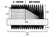
図5に示す構成において、最初に、厚さ0.075mmのPETフィルムを基板20として、この基板20の片面側に、均一濃度部と濃度勾配領域とを有する、多層薄膜で構成されたグラデーションND膜21を形成した。濃度勾配領域の形成にあたっては、本実施例では各成膜基板上の成膜面側に図3で示すようなマスクを設置し成膜する手法を選択した。このようなグラデーションND膜21は、本実施例では図4(a)で示すような積層構造とした。
In the configuration shown in FIG. 5, first, a gradation film ND composed of a multilayer thin film having a uniform density portion and a density gradient region on one side of the
ここで、グラデーションND膜21の膜構成において、本実施例では、図5に示す構成において、密着層24をグラデーションND膜21の最表層とみなして、密着層24と微細構造体22との界面での反射を無視し、グラデーションND膜21を構成するそれ以外の多層膜間の各界面での反射を光干渉効果により相殺させる膜構成とした。
Here, in the film configuration of the gradation ND film 21, in this embodiment, in the configuration shown in FIG. 5, the
以上のように作製されたグラデーションND膜21上に密着層24を介し微細構造体22を形成し、基板上のもう一方の面にも第2の微細構造体23をそれぞれ形成した。微細構造体の作製に関しては、本実施例ではUV硬化樹脂を用いた光ナノインプリント法を選択した。
A
まず、グラデーションND膜21の最表層と微細構造体22との密着性を向上させる為に、プライマー処理を行い、これらの界面に密着層24を設けた。このようなプライマー溶液の例としては、シランカップリング剤をベースに、IPAや硝酸等を適量加え、さらにTEOSを加えたものを用いた。これを、0.2μmのPTFEフィルタを介し基板上に滴下し、スピンコートにより極薄膜となるように塗工した後、所定の条件で乾燥処理等を行い、密着層24を形成する。
First, in order to improve the adhesion between the outermost layer of the gradation ND film 21 and the
この際、より高い反射低減効果を得る為に、本実施例2においては、密着層24の波長540nmでの屈折率は1.47となるように調整しており、グラデーションND膜21との界面層となる、グラデーションND膜21の最表層SiO2の屈折率は1.46、微細構造体22の屈折率は1.51であるから、密着層のそれぞれの界面での屈折率差を、0.01、0.04とし、0.05以下とする構成とした。
At this time, in order to obtain a higher reflection reduction effect, in Example 2, the refractive index at the wavelength 540 nm of the
本実施例2における微細構造体22、第2の微細構造体23は、図1で示したような突起構造を周期的に配置したピラーアレイ状とし、構造体は釣鐘型のモス・アイ形状で構造体の周期は約250nmとした。さらに、突起構造体の配列は三方配列とした。
The
また図5で示すように、均一濃度領域では微細構造体22は略同じ構造高さであるが、濃度勾配領域ではグラデーションND膜21の膜厚が厚いほど構造高さが高くなるように構成した。より具体的には均一濃度領域では構造高さは約250nmとし、さらに濃度勾配領域では構造高さは約250nm〜500nmの高低差を有する構造とした。さらに、基板のもう一方の面に形成した第2の微細構造体23は全領域で略同じ250nmの構造高さとした。
Further, as shown in FIG. 5, the
まず、基板上にUV硬化樹脂を0.2μmのPTFEフィルタを介し適量滴下した後、スピンコート法により所定の膜厚となるように基板全面にUV硬化樹脂を塗工した。その後、この基板に、樹脂の硬化収縮を加味し、所望する形状を反転させ設計されたホールアレイ形状に離型処理を施した石英モールドを押し当て、少しの時間この状態を保持した後、そのままの状態でUV光を照射することで樹脂を硬化させ、微細構造体22を作製した。
First, an appropriate amount of a UV curable resin was dropped on a substrate through a 0.2 μm PTFE filter, and then the UV curable resin was applied to the entire surface of the substrate so as to have a predetermined film thickness by spin coating. After that, the quartz mold that has been subjected to mold release processing is pressed against the designed hole array by reversing the desired shape, taking into account the curing shrinkage of the resin, and this state is maintained for a short time. In this state, the resin was cured by irradiating UV light, and the
その後、基板の表裏を反転させ、基板上のもう一方の面に、同様の方法で第2の微細構造体23を作製した。この際、本実施例では、基板20直上に直接第2の微細構造体23を形成したが、この界面に密着層を挿入しても良い。
Thereafter, the front and back of the substrate were reversed, and a
以上によって作製されたNDフィルタ25は、グラデーションND膜21の膜厚に合わせ、濃度勾配領域の膜厚差に起因した位相差を低減するように、構造高さを調整した反射低減効果の高い微細構造体22を形成し、更に基板のもう一方の面にも、反射低減効果の高い第2の微細構造体23を形成することで、フィルタ内の全域において、反射を十分に低減し、同時に位相差を低減することが可能である。
The
また、本実施例2では、ナノインプリントプロセスを2回繰り返すことで、基板の両面に微細構造体を形成したが、スピンコートや、ディップコートなどにより樹脂を基板表裏へ塗工した後、両面を同時にUVナノインプリントすることでも同様の微細構造体を形成することができる。 In Example 2, the nanoimprint process was repeated twice to form fine structures on both sides of the substrate. However, after applying the resin to the front and back of the substrate by spin coating or dip coating, both sides were simultaneously coated. A similar microstructure can be formed by UV nanoimprinting.
(実施例3)
図6(a)〜(b)に示した、実施例1、及び実施例2に記載した以外の、その他の構成例について、以下に詳細を記載する。また、本実施例3においては、基板は0.075mmのPETフィルムを用いており、さらにND膜と微細構造体との界面には、実施例1、実施例2で用いた極薄の密着層を設けている。一方で、基板上に微細構造体を直接形成する場合には密着層を設けていないが、それぞれの界面において必要に応じて密着層を挿入することも可能である。
Example 3
Details of other configuration examples other than those described in the first and second embodiments illustrated in FIGS. 6A to 6B will be described below. In Example 3, a 0.075 mm PET film is used as the substrate, and the ultrathin adhesive layer used in Examples 1 and 2 is used at the interface between the ND film and the fine structure. Is provided. On the other hand, when the fine structure is directly formed on the substrate, the adhesion layer is not provided, but it is possible to insert the adhesion layer as necessary at each interface.
(実施例2)
図6(a)は実施例2の構成をベースに、NDフィルタ37内に、膜厚が一定の均一濃度領域と、膜厚が連続的に変化している濃度勾配領域に加え、透明領域を設けたことが特徴であり、微細構造体33の構造高さを調整することで、NDフィルタ37の透明領域を含む領域の、入射光に対する反射と位相差を同時に低減した構成例である。このような構成とすることで、透明部を有するタイプのNDフィルタにも本発明の構成を適用することが可能である。
(Example 2)
FIG. 6A is based on the configuration of the second embodiment. In the
図6(b)はグラデーションND膜31の均一濃度領域、及び濃度勾配領域上に設けた微細構造体33の構造高さは略一定とし、基板裏面に形成した第2の微細構造体34の濃度勾配領域における構造高さを調整したことに特徴があり、これによりNDフィルタ37における入射光に対する反射と位相差を同時に低減した構成例である。
FIG. 6B shows the uniform density region of the
また、グラデーションND膜31の濃度勾配領域上に設けた微細構造体33の構造高さを変化させることに加え、さらに基板裏面に形成した第2の微細構造体34の濃度勾配領域における構造高さを調整してもよい。これは、NDフィルタ37の全領域における入射光に対する反射と位相差を同時に低減した構成例である。このような構成とすることで、位相差を低減する為に必要な構造体高さを、基板表裏で分割することができる為、1つの微細構造体における構造高さを低く設定することが可能となる。構造高さを低くすることで、形成された微細構造の剛性が高まると共に、本実施例1及び本実施例2に記載したナノインプリントプロセスなど、微細構造体の形成プロセスでの生産性をより高めることができる。
Further, in addition to changing the structural height of the
グラデーションND膜31の濃度勾配領域上に設けた微細構造体33の構造高さを変化させ、さらに微細構造体33の構造高さだけではなく、基板30を基準とし、基板30からの高さ位置も異なるように形成してもよい。これは、NDフィルタ37の全領域における入射光に対する反射と位相差を同時に低減した構成例である。このような構成とすることで、微細構造体における位相差調整の幅が拡がり、微細構造体による位相差低減効果をより大きくすることが可能となる。
Change the structural height of the
基板両面に、膜厚が一定の均一濃度領域と、膜厚が連続的に変化している濃度勾配領域とを有する、多層薄膜で構成されたグラデーションND膜31と第2のグラデーション膜32を構成し、さらに均一濃度領域と濃度勾配領域との境界位置が基板の両面で略同じ位置となるように配置してもよい。これは、NDフィルタ37の全領域における反射と位相差を同時に低減した構成例である。
The board both surfaces, and the thickness is constant uniform density region has a concentration gradient region where the film thickness varies continuously, the
前段落で説明した構成の変形例として、基板両面に、膜厚が一定の均一濃度領域と、膜厚が連続的に変化している濃度勾配領域とを有する、多層薄膜で構成されたグラデーションND膜31と第2のグラデーション膜32を構成し、さらに均一濃度領域と濃度勾配領域との境界位置が基板の両面で異なるように配置してもよい。これは、NDフィルタ37の全領域における反射と位相差を同時に低減した構成例である。前段落で説明した構成とすることで、基板両面に分割配置されたグラデーションNDフィルタを作製することが可能となり、例えば基板両面での分光反射率特性をより近い分散形状に調整することなどができ、さらには高濃度のNDフィルタに対応することが可能となる。
As a modification of the configuration described in the previous paragraph, a gradation ND composed of a multilayer thin film having a uniform concentration region with a constant film thickness and a concentration gradient region with a continuously changing film thickness on both surfaces of the substrate. The
更に、同一フィルタ内に複数の濃度領域を持つ、段階的に濃度変化する多濃度タイプのNDフィルタに応用することも可能である。基本的には膜厚が厚いほど濃度が高い領域となり、多濃度ND膜39の各濃度領域における膜厚に合わせ、位相差を低減するように微細構造体33の構造高さを調整する。濃度領域は2つ以上であれば多濃度タイプのNDフィルタとして機能させることが可能である。
Further, the with multiple density regions within the same filter, it is also possible to stepwise applied to the ND filter of the multi-density type of concentration change. Basically, the thicker the film thickness is, the higher the concentration is, and the structure height of the
また、これらの構成に限定されず、実施例1、2の構成を含み、それぞれ構成で特徴とされる部分を2つ以上組み合わせた構成とすることも可能であり、適宜最適な構成を選択することが可能である。 In addition, the present invention is not limited to these configurations, and the configurations of the first and second embodiments may be included, and a configuration in which two or more portions each characterized by the configuration are combined may be used. The optimal configuration is appropriately selected. It is possible.
さらには、本実施例1〜3においては、微細構造体の高さを調整することで、位相差を低減する方法を選択したが、これに限らず、例えば図7(a)(b)で示すように微細構造の外形形状を調整することでも位相差低減が可能であるし、高さを含めたこれらの要素を組み合わせ低減することも可能である。 Furthermore, in the first to third embodiments, the method of reducing the phase difference was selected by adjusting the height of the fine structure. However, the present invention is not limited to this. For example, in FIGS. As shown, the phase difference can be reduced by adjusting the outer shape of the fine structure, and these elements including the height can be combined and reduced.
本実施例1〜3に示したような基本構成を他の光学フィルタに応用することも可能である。例えば、フィルタを出し入れする機構を有する監視カメラなどに用いられるIRカットフィルタやUVIRカットフィルタなどが挙げられる。このようなIRカットフィルタの場合、フィルタの有無によって光学系に光路差が生じてしまい、撮像素子の配置位置と焦点位置とが変わってしまう為、画像が劣化してしまう場合があるが、この光路差(位相差)を低減する為に、透明なガラスやフィルムなどの透明フィルタをダミーとして挿入することがある。しかし、多層薄膜などで構成されたIRカット膜などでは、IRカットフィルタと透明フィルタとで生じる、膜厚差に起因した位相差までを改善することは難しい。そこで、透明フィルタの基板上に光の波長サイズよりも短いピッチで無数に配置された微細構造により構成された反射低減効果を有する微細構造体を形成し、更にはこの微細構造体の構造高さなどを調整し、入射光に対しIRカット膜を透過することで生じる位相差分を低減するように微細構造形状を調整することで、透明フィルタでの反射と、IRカットフィルタと透明フィルタとの位相差を低減することが可能である。またこの場合、IRカットフィルタにおいて、IRカット膜上に反射低減効果を持つ微細構造体を形成し、位相差を調整することも可能である。 The basic configuration as shown in the first to third embodiments can be applied to other optical filters. For example, an IR cut filter or a UVIR cut filter used for a surveillance camera having a mechanism for inserting and removing the filter can be used. In the case of such an IR cut filter, an optical path difference occurs in the optical system depending on the presence or absence of the filter, and the image sensor may be deteriorated because the arrangement position and the focal position of the image sensor are changed. In order to reduce the optical path difference (phase difference), a transparent filter such as transparent glass or film may be inserted as a dummy. However, with an IR cut film composed of a multilayer thin film or the like, it is difficult to improve even the phase difference caused by the film thickness difference between the IR cut filter and the transparent filter. Therefore, a microstructure having a reflection reducing effect is formed on the substrate of the transparent filter and has a reflection reducing effect constituted by countless microstructures arranged at a pitch shorter than the wavelength of light, and the structural height of the microstructure is further increased. By adjusting the fine structure shape so as to reduce the phase difference that occurs when the incident light is transmitted through the IR cut film, the reflection by the transparent filter and the position of the IR cut filter and the transparent filter are adjusted. It is possible to reduce the phase difference. In this case, in the IR cut filter, it is also possible to adjust the phase difference by forming a fine structure having a reflection reducing effect on the IR cut film.
さらには、IRカットフィルタと透明フィルタの機能を1枚の基板上に形成し、即ち、IRカット膜を有するIRカット領域と、IRカット膜を有さない透明領域とを同一基板上に設け、さらに光の波長サイズよりも短いピッチで無数に配置された微細構造により構成された反射低減効果を有する微細構造体を、IRカット膜を透過する光と、IRカット膜を透過しない光との間で生じる位相差を低減するように、IRカット領域と透明領域とでそれぞれ微細構造形状を調整し配置することで、IRカットフィルタの反射と位相差を同時に低減することが可能である。 Furthermore, the functions of an IR cut filter and a transparent filter are formed on a single substrate, that is, an IR cut region having an IR cut film and a transparent region having no IR cut film are provided on the same substrate. Furthermore, a fine structure having a reflection reducing effect constituted by a fine structure arranged innumerably at a pitch shorter than the wavelength size of light, between the light that passes through the IR cut film and the light that does not pass through the IR cut film. It is possible to simultaneously reduce reflection and phase difference of the IR cut filter by adjusting and arranging the fine structure shapes in the IR cut region and the transparent region so as to reduce the phase difference generated in FIG.
このように、膜厚の異なる複数の領域を持つ光学フィルタや、膜厚の異なる複数の光学フィルタを使用する光学装置において、各領域や各フィルタを形成する膜上に、反射低減効果を有する光の波長サイズよりも短いピッチで無数に配置された微細構造により構成された微細構造体を形成し、さらには、入射光に対し、それぞれの膜厚に起因した位相差を低減するように微細構造形状を調整することで、光学フィルタの反射を低減しつつ、位相差を低減することが可能であり、高精度化を図ることが可能となる。 As described above, in an optical filter having a plurality of regions having different film thicknesses or an optical device using a plurality of optical filters having different film thicknesses, light having a reflection reducing effect on each region or a film forming each filter. Forming a fine structure composed of countless fine structures arranged at a pitch shorter than the wavelength size of the light, and further reducing the phase difference due to the respective film thicknesses against incident light By adjusting the shape, it is possible to reduce the phase difference while reducing the reflection of the optical filter, and it is possible to achieve high accuracy.
(実施例5)
次に、本実施例1〜3で作製したNDフィルタを、光量絞り装置に適用した実施例について図8を用いて説明する。
(Example 5)
Next, an embodiment in which the ND filter produced in the first to third embodiments is applied to a light quantity diaphragm device will be described with reference to FIG.
図8に光量絞り装置を示す。ビデオカメラあるいはデジタルスチルカメラ等の撮像系に使用するに適した光量絞り装置の絞りは、CCDやCMOSセンサと言った固体撮像素子への入射光量を制御するために設けられているものである。被写界が明るくなるにつれ、絞り羽根41を制御し、より小さく絞り込まれていく構造になっている。このとき、小絞り状態時に発生する像性能の劣化に対する対策として、絞りの近傍にNDフィルタ44を配置し、被写界の明るさが同一であっても、絞りの開口をより大きくできる構造にしている。入射光がこの光量絞り装置43を通過し、固体撮像素子(不図示)に到達することで電気的な信号に変換され画像が形成される。
FIG. 8 shows a light quantity diaphragm device. A diaphragm of a light amount diaphragm device suitable for use in an imaging system such as a video camera or a digital still camera is provided for controlling the amount of light incident on a solid-state imaging device such as a CCD or CMOS sensor. As the field of view becomes brighter, the
この光量絞り装置43に、本実施例1〜3で作製されたNDフィルタを配置する。更には、NDフィルタ44を絞り羽根支持板42に固定するように配置することも可能である。この場合、NDフィルタを配置する位置や、光量絞り装置43のメカ的な機構にも依存するが、本実施例で作製したフィルタと必要な外形が異なる場合も想定されるが、最適な形状を選択すればよい。
The ND filter produced in the first to third embodiments is disposed in the light
(実施例6)
次に、本実施例1〜3で作製した光学フィルタを備えるビデオカメラ等の撮影装置に適用した実施例について図9を用いて説明する。
(Example 6)
Next, an embodiment applied to a photographing apparatus such as a video camera provided with the optical filter produced in the first to third embodiments will be described with reference to FIG.
図9は、ビデオカメラなどの撮影装置で、絞り羽根55やレンズユニット51A〜51Dなどで構成された撮影光学系51を透過した光線を、NDフィルタ54で固体撮像素子52の特性に合わせて制限し、適正な画像を得るようになっている。51はレンズユニット51A〜51Dを有する撮影光学系である。52はCCD等の固体撮像素子であり、撮影光学系51によって形成される光線a、bの像を受光し、電気信号に変換する。53は光学ローパスフィルタである。撮像光学系51は、図9に示したNDフィルタ54、絞り羽根55、56、地板57で構成される光量絞り装置を有している。
FIG. 9 shows a photographing apparatus such as a video camera. Light rays that have passed through the photographing
このNDフィルタ54の位置に、本実施例1〜3で作製されたNDフィルタ54の部分に配置する。これらのフィルタは出し入れ自由に駆動することも可能である。より具体的には、撮影光学系51を透過して撮像素子52に結像した光量を判断して、NDフィルタ54を駆動する。入射した光量が通常の撮影に過剰な場合には、固体撮像素子52にかかるようにNDフィルタ54を移動させる。逆に光量が不十分なときは、固体撮像素子52にかからないように光路外に退避させる。NDフィルタ54の有無により、結像する光線に光路差が発生してしまい、画像が劣化してしまうことがあるが、このような場合には光学フィルタの基材と同じ材質の基材をダミーとして挿入したり、図6(a)のようにNDフィルタ54に透明部を設けておき、この領域を使用したりすることで、画像劣化を抑えることができる。
At the position of the
これにより作製された撮像装置は、入射光に対するフィルタの反射と、位相差に起因した画像劣化などの不具合を著しく低減することができる。 The imaging device thus manufactured can remarkably reduce inconveniences such as reflection of the filter with respect to incident light and image degradation due to the phase difference.
これに限らず、他の光学装置であっても、実施例1〜3で作製したようなNDフィルタを用いることで、フィルタの反射と位相差に起因した装置上の不具合を著しく低減することができ、これより高精度化を実現することが可能である。 Not only this but also other optical devices, by using the ND filter as produced in Examples 1 to 3, it is possible to remarkably reduce problems on the device due to the reflection and phase difference of the filter. It is possible to achieve higher accuracy than this.
10、20、30.基板
11、21、31.グラデーションND膜
32.第2のグラデーションND膜
12、22、33.微細構造体
23、34.第2の微細構造体
13、24、35、36.密着層
14、38.反射防止膜
15、25、37.NDフィルタ
39.多濃度ND膜
16.マスク
17.遮蔽板
41.絞り羽根
42.絞り羽根指示板
43.光量絞り装置
44.NDフィルタ
51.撮影光学系
52.固体撮像素子
53.光学ローパスフィルタ
54.NDフィルタ
55.絞り羽根
56.絞り羽根
57.地板
10, 20, 30.
16.
41.
51. Shooting
Claims (10)
前記透明基板上に設けられた機能膜と、を備え、
前記機能膜は、前記透明基板上に設けられた膜厚が異なる複数の領域が形成された光学膜と、前記光学膜上に設けられた光の波長サイズよりも短いピッチで複数の微細構造が形成された微細構造体と、を有し、
前記微細構造体は、前記微細構造の形状を前記複数の領域でそれぞれ異なる形状としたことを特徴とする光学フィルタ。 A transparent substrate that transmits light in the visible wavelength region;
A functional film provided on the transparent substrate,
The functional film includes an optical film having a plurality of regions having different film thicknesses provided on the transparent substrate, and a plurality of microstructures at a pitch shorter than the wavelength size of light provided on the optical film. A formed microstructure, and
The optical filter according to claim 1, wherein the microstructure has a shape different from that of the plurality of regions.
前記他の微細構造の形状をそれぞれ変化させたことを特徴とする、
請求項4に記載の光学フィルタ。 In order to reduce the phase difference of incident light in the plurality of regions,
The shape of the other fine structure is changed, respectively,
The optical filter according to claim 4.
請求項5に記載の光学フィルタ。 The shape of the other microstructure is characterized by a structure height of the other fine structures,
The optical filter according to claim 5.
前記透明基板上に設けられた機能膜と、を備え、
前記機能膜は、前記透明基板上に設けられた膜厚が異なる複数の領域が形成された光学膜と、前記光学膜上に設けられた光の波長サイズよりも短いピッチで複数の微細構造から形成された微細構造体と、を有し、
前記微細構造体は、前記光学膜の膜厚変化に応じて異なる形状の微細構造を有することを特徴とする光学フィルタ。 A transparent substrate that transmits light in the visible wavelength region;
A functional film provided on the transparent substrate,
The functional film includes an optical film provided with a plurality of regions having different thicknesses provided on the transparent substrate, and a plurality of microstructures at a pitch shorter than a wavelength size of light provided on the optical film. A formed microstructure, and
The optical filter, wherein the fine structure has a fine structure having a different shape according to a change in the thickness of the optical film.
Priority Applications (1)
| Application Number | Priority Date | Filing Date | Title |
|---|---|---|---|
| JP2015133961A JP6556529B2 (en) | 2015-07-02 | 2015-07-02 | Optical filter and optical device provided with optical filter |
Applications Claiming Priority (1)
| Application Number | Priority Date | Filing Date | Title |
|---|---|---|---|
| JP2015133961A JP6556529B2 (en) | 2015-07-02 | 2015-07-02 | Optical filter and optical device provided with optical filter |
Publications (3)
| Publication Number | Publication Date |
|---|---|
| JP2017015999A JP2017015999A (en) | 2017-01-19 |
| JP2017015999A5 JP2017015999A5 (en) | 2018-08-09 |
| JP6556529B2 true JP6556529B2 (en) | 2019-08-07 |
Family
ID=57830631
Family Applications (1)
| Application Number | Title | Priority Date | Filing Date |
|---|---|---|---|
| JP2015133961A Active JP6556529B2 (en) | 2015-07-02 | 2015-07-02 | Optical filter and optical device provided with optical filter |
Country Status (1)
| Country | Link |
|---|---|
| JP (1) | JP6556529B2 (en) |
Families Citing this family (3)
| Publication number | Priority date | Publication date | Assignee | Title |
|---|---|---|---|---|
| JP6827279B2 (en) * | 2016-07-15 | 2021-02-10 | 日立ジョンソンコントロールズ空調株式会社 | Cooling / heating switching unit and air conditioner equipped with it |
| JP7378114B2 (en) * | 2019-03-15 | 2023-11-13 | 東海光学株式会社 | ND filter |
| JP6923064B1 (en) * | 2020-12-15 | 2021-08-18 | 東洋インキScホールディングス株式会社 | Laminates and wavelength cut filters |
Family Cites Families (7)
| Publication number | Priority date | Publication date | Assignee | Title |
|---|---|---|---|---|
| JP4801442B2 (en) * | 2005-12-28 | 2011-10-26 | キヤノン電子株式会社 | ND filter for diaphragm |
| JP4988282B2 (en) * | 2006-09-22 | 2012-08-01 | キヤノン電子株式会社 | Optical filter |
| JP2010175941A (en) * | 2009-01-30 | 2010-08-12 | Canon Electronics Inc | Optical filter and method of manufacturing the same, and image capturing apparatus having the same |
| JP5600396B2 (en) * | 2009-04-23 | 2014-10-01 | キヤノン電子株式会社 | Optical filter |
| EP2711742A4 (en) * | 2011-05-17 | 2014-10-29 | Canon Denshi Kk | Optical filter, optical device, electronic device, and antireflection complex |
| JP6053352B2 (en) * | 2011-06-29 | 2016-12-27 | キヤノン電子株式会社 | Optical filter, optical device, and optical filter manufacturing method. |
| JP2013041027A (en) * | 2011-08-12 | 2013-02-28 | Canon Electronics Inc | Optical filter |
-
2015
- 2015-07-02 JP JP2015133961A patent/JP6556529B2/en active Active
Also Published As
| Publication number | Publication date |
|---|---|
| JP2017015999A (en) | 2017-01-19 |
Similar Documents
| Publication | Publication Date | Title |
|---|---|---|
| JP5728572B2 (en) | Optical filter and optical device | |
| JP6317954B2 (en) | Lens unit, imaging module, and electronic device | |
| US9759847B2 (en) | Optical filter | |
| KR101483386B1 (en) | Optical filter, method for producing same, and image capturing device | |
| JP6006718B2 (en) | Optical filter, optical device, electronic device, and antireflection composite | |
| US9513417B2 (en) | Optical filter and optical apparatus | |
| JP6790831B2 (en) | Optical filter and imaging device | |
| JP2008051985A (en) | Near infrared ray absorbing filter | |
| JP2012137649A (en) | Optical filter | |
| TW202205001A (en) | Camera structure and image capturing device | |
| JP4801442B2 (en) | ND filter for diaphragm | |
| JP2012137648A (en) | Imaging optical unit | |
| JP6556529B2 (en) | Optical filter and optical device provided with optical filter | |
| JP2013015827A (en) | Nd filter and optical device | |
| JP6053352B2 (en) | Optical filter, optical device, and optical filter manufacturing method. | |
| JP2010066704A (en) | Optical element, optical system, and optical apparatus | |
| JP4671410B2 (en) | Light aperture device and camera with ND filter with IR cut function | |
| JP2015011319A (en) | Near-infrared cut filter | |
| JP6162947B2 (en) | Optical filter, optical device, electronic device | |
| JP6980364B2 (en) | Optical filter, light intensity adjuster and optical device | |
| JP2018180430A (en) | Optical filter | |
| JP6224314B2 (en) | Optical filter and optical apparatus | |
| JP6386785B2 (en) | MICROSTRUCTURE, OPTICAL FILTER AND OPTICAL DEVICE | |
| JP6761231B2 (en) | Antireflection microstructures, optical filters, optics, and methods for manufacturing antireflection microstructures | |
| JP2007316238A (en) | Nd filter |
Legal Events
| Date | Code | Title | Description |
|---|---|---|---|
| A521 | Request for written amendment filed |
Free format text: JAPANESE INTERMEDIATE CODE: A523 Effective date: 20180629 |
|
| A621 | Written request for application examination |
Free format text: JAPANESE INTERMEDIATE CODE: A621 Effective date: 20180702 |
|
| RD03 | Notification of appointment of power of attorney |
Free format text: JAPANESE INTERMEDIATE CODE: A7423 Effective date: 20180702 |
|
| A621 | Written request for application examination |
Free format text: JAPANESE INTERMEDIATE CODE: A621 Effective date: 20180702 |
|
| A977 | Report on retrieval |
Free format text: JAPANESE INTERMEDIATE CODE: A971007 Effective date: 20190314 |
|
| A131 | Notification of reasons for refusal |
Free format text: JAPANESE INTERMEDIATE CODE: A131 Effective date: 20190322 |
|
| A521 | Request for written amendment filed |
Free format text: JAPANESE INTERMEDIATE CODE: A523 Effective date: 20190515 |
|
| TRDD | Decision of grant or rejection written | ||
| A01 | Written decision to grant a patent or to grant a registration (utility model) |
Free format text: JAPANESE INTERMEDIATE CODE: A01 Effective date: 20190614 |
|
| A61 | First payment of annual fees (during grant procedure) |
Free format text: JAPANESE INTERMEDIATE CODE: A61 Effective date: 20190710 |
|
| R150 | Certificate of patent or registration of utility model |
Ref document number: 6556529 Country of ref document: JP Free format text: JAPANESE INTERMEDIATE CODE: R150 |
|
| R250 | Receipt of annual fees |
Free format text: JAPANESE INTERMEDIATE CODE: R250 |
|
| R250 | Receipt of annual fees |
Free format text: JAPANESE INTERMEDIATE CODE: R250 |