WO2012153687A1 - パネル複合体、表示装置及びパネル複合体の製造方法 - Google Patents
パネル複合体、表示装置及びパネル複合体の製造方法 Download PDFInfo
- Publication number
- WO2012153687A1 WO2012153687A1 PCT/JP2012/061587 JP2012061587W WO2012153687A1 WO 2012153687 A1 WO2012153687 A1 WO 2012153687A1 JP 2012061587 W JP2012061587 W JP 2012061587W WO 2012153687 A1 WO2012153687 A1 WO 2012153687A1
- Authority
- WO
- WIPO (PCT)
- Prior art keywords
- substrate
- panel
- polarizing plate
- plate
- adhesive
- Prior art date
- Legal status (The legal status is an assumption and is not a legal conclusion. Google has not performed a legal analysis and makes no representation as to the accuracy of the status listed.)
- Ceased
Links
Images




Classifications
-
- G—PHYSICS
- G02—OPTICS
- G02F—OPTICAL DEVICES OR ARRANGEMENTS FOR THE CONTROL OF LIGHT BY MODIFICATION OF THE OPTICAL PROPERTIES OF THE MEDIA OF THE ELEMENTS INVOLVED THEREIN; NON-LINEAR OPTICS; FREQUENCY-CHANGING OF LIGHT; OPTICAL LOGIC ELEMENTS; OPTICAL ANALOGUE/DIGITAL CONVERTERS
- G02F1/00—Devices or arrangements for the control of the intensity, colour, phase, polarisation or direction of light arriving from an independent light source, e.g. switching, gating or modulating; Non-linear optics
- G02F1/01—Devices or arrangements for the control of the intensity, colour, phase, polarisation or direction of light arriving from an independent light source, e.g. switching, gating or modulating; Non-linear optics for the control of the intensity, phase, polarisation or colour
- G02F1/13—Devices or arrangements for the control of the intensity, colour, phase, polarisation or direction of light arriving from an independent light source, e.g. switching, gating or modulating; Non-linear optics for the control of the intensity, phase, polarisation or colour based on liquid crystals, e.g. single liquid crystal display cells
- G02F1/133—Constructional arrangements; Operation of liquid crystal cells; Circuit arrangements
- G02F1/1333—Constructional arrangements; Manufacturing methods
- G02F1/133308—Support structures for LCD panels, e.g. frames or bezels
-
- G—PHYSICS
- G02—OPTICS
- G02F—OPTICAL DEVICES OR ARRANGEMENTS FOR THE CONTROL OF LIGHT BY MODIFICATION OF THE OPTICAL PROPERTIES OF THE MEDIA OF THE ELEMENTS INVOLVED THEREIN; NON-LINEAR OPTICS; FREQUENCY-CHANGING OF LIGHT; OPTICAL LOGIC ELEMENTS; OPTICAL ANALOGUE/DIGITAL CONVERTERS
- G02F1/00—Devices or arrangements for the control of the intensity, colour, phase, polarisation or direction of light arriving from an independent light source, e.g. switching, gating or modulating; Non-linear optics
- G02F1/01—Devices or arrangements for the control of the intensity, colour, phase, polarisation or direction of light arriving from an independent light source, e.g. switching, gating or modulating; Non-linear optics for the control of the intensity, phase, polarisation or colour
- G02F1/13—Devices or arrangements for the control of the intensity, colour, phase, polarisation or direction of light arriving from an independent light source, e.g. switching, gating or modulating; Non-linear optics for the control of the intensity, phase, polarisation or colour based on liquid crystals, e.g. single liquid crystal display cells
- G02F1/133—Constructional arrangements; Operation of liquid crystal cells; Circuit arrangements
- G02F1/1333—Constructional arrangements; Manufacturing methods
- G02F1/1347—Arrangement of liquid crystal layers or cells in which the final condition of one light beam is achieved by the addition of the effects of two or more layers or cells
- G02F1/13471—Arrangement of liquid crystal layers or cells in which the final condition of one light beam is achieved by the addition of the effects of two or more layers or cells in which all the liquid crystal cells or layers remain transparent, e.g. FLC, ECB, DAP, HAN, TN, STN, SBE-LC cells
-
- G—PHYSICS
- G02—OPTICS
- G02F—OPTICAL DEVICES OR ARRANGEMENTS FOR THE CONTROL OF LIGHT BY MODIFICATION OF THE OPTICAL PROPERTIES OF THE MEDIA OF THE ELEMENTS INVOLVED THEREIN; NON-LINEAR OPTICS; FREQUENCY-CHANGING OF LIGHT; OPTICAL LOGIC ELEMENTS; OPTICAL ANALOGUE/DIGITAL CONVERTERS
- G02F1/00—Devices or arrangements for the control of the intensity, colour, phase, polarisation or direction of light arriving from an independent light source, e.g. switching, gating or modulating; Non-linear optics
- G02F1/01—Devices or arrangements for the control of the intensity, colour, phase, polarisation or direction of light arriving from an independent light source, e.g. switching, gating or modulating; Non-linear optics for the control of the intensity, phase, polarisation or colour
- G02F1/13—Devices or arrangements for the control of the intensity, colour, phase, polarisation or direction of light arriving from an independent light source, e.g. switching, gating or modulating; Non-linear optics for the control of the intensity, phase, polarisation or colour based on liquid crystals, e.g. single liquid crystal display cells
- G02F1/133—Constructional arrangements; Operation of liquid crystal cells; Circuit arrangements
- G02F1/1333—Constructional arrangements; Manufacturing methods
- G02F1/1335—Structural association of cells with optical devices, e.g. polarisers or reflectors
- G02F1/133528—Polarisers
-
- G—PHYSICS
- G02—OPTICS
- G02F—OPTICAL DEVICES OR ARRANGEMENTS FOR THE CONTROL OF LIGHT BY MODIFICATION OF THE OPTICAL PROPERTIES OF THE MEDIA OF THE ELEMENTS INVOLVED THEREIN; NON-LINEAR OPTICS; FREQUENCY-CHANGING OF LIGHT; OPTICAL LOGIC ELEMENTS; OPTICAL ANALOGUE/DIGITAL CONVERTERS
- G02F1/00—Devices or arrangements for the control of the intensity, colour, phase, polarisation or direction of light arriving from an independent light source, e.g. switching, gating or modulating; Non-linear optics
- G02F1/01—Devices or arrangements for the control of the intensity, colour, phase, polarisation or direction of light arriving from an independent light source, e.g. switching, gating or modulating; Non-linear optics for the control of the intensity, phase, polarisation or colour
- G02F1/13—Devices or arrangements for the control of the intensity, colour, phase, polarisation or direction of light arriving from an independent light source, e.g. switching, gating or modulating; Non-linear optics for the control of the intensity, phase, polarisation or colour based on liquid crystals, e.g. single liquid crystal display cells
- G02F1/133—Constructional arrangements; Operation of liquid crystal cells; Circuit arrangements
- G02F1/1333—Constructional arrangements; Manufacturing methods
- G02F1/13338—Input devices, e.g. touch panels
-
- G—PHYSICS
- G02—OPTICS
- G02F—OPTICAL DEVICES OR ARRANGEMENTS FOR THE CONTROL OF LIGHT BY MODIFICATION OF THE OPTICAL PROPERTIES OF THE MEDIA OF THE ELEMENTS INVOLVED THEREIN; NON-LINEAR OPTICS; FREQUENCY-CHANGING OF LIGHT; OPTICAL LOGIC ELEMENTS; OPTICAL ANALOGUE/DIGITAL CONVERTERS
- G02F2201/00—Constructional arrangements not provided for in groups G02F1/00 - G02F7/00
- G02F2201/50—Protective arrangements
- G02F2201/503—Arrangements improving the resistance to shock
-
- G—PHYSICS
- G02—OPTICS
- G02F—OPTICAL DEVICES OR ARRANGEMENTS FOR THE CONTROL OF LIGHT BY MODIFICATION OF THE OPTICAL PROPERTIES OF THE MEDIA OF THE ELEMENTS INVOLVED THEREIN; NON-LINEAR OPTICS; FREQUENCY-CHANGING OF LIGHT; OPTICAL LOGIC ELEMENTS; OPTICAL ANALOGUE/DIGITAL CONVERTERS
- G02F2202/00—Materials and properties
- G02F2202/28—Adhesive materials or arrangements
Definitions
- the present invention relates to a panel composite, a display device, and a method for manufacturing the panel composite.
- a display device including a liquid crystal panel that displays an image and the like and a functional panel such as a touch panel, a viewing angle control panel, and a parallax barrier panel is known (for example, see Patent Document 1).
- the functional panel as a sub-panel is attached to the surface of the liquid crystal panel as a main panel via an adhesive.
- a photo-curing (photosensitive) adhesive is generally used as the adhesive.
- This photo-curable adhesive is liquid before being cured by being irradiated with light such as ultraviolet rays, and has fluidity.
- the adhesive having the fluidity is first applied on the surface of the main panel.
- the sub panel is overlaid on the surface of the main panel so as to sandwich the applied adhesive.
- the main panel and the sub panel are respectively positioned, and further, the adhesive is irradiated with light such as ultraviolet rays, so that the main panel and the sub panel are bonded.
- the adhesive layer interposed between the main panel and the sub panel is not uniform, the distance (interval) between the main panel and the sub panel will vary. Then, display unevenness such as color unevenness may occur in the image of the main panel visually recognized by the user through the sub panel. Therefore, the adhesive is thinly spread so as to be sandwiched and flattened between the main panel and the sub-panel in a state having fluidity so that the thickness of the adhesive layer is uniform. ing.
- a polarizing plate is usually provided on the outermost surface of the main panel (liquid crystal panel). Therefore, specifically, the adhesive is spread thinly between the polarizing plate and the sub panel as described above. Since the polarizing plate is usually set to be slightly smaller than the main body portion (liquid crystal panel) of the main panel, the peripheral edge of the polarizing plate is recessed inside the peripheral edge of the main panel.
- the polarizing plate is easily affected by humidity and swells when it absorbs moisture (humidity) in the outside air, so its thickness may change. Then, the swollen polarizing plate may cause display unevenness as described above. Therefore, the periphery of the polarizing plate is covered with the adhesive.
- An object of the present invention is a panel composite including a main panel and an object attached to the main panel, and a technique for suppressing the adhesive disposed between them from protruding outward from the end of the panel composite. Is to provide.
- the panel composite according to the present invention is a pair of large and small substrates bonded so that their inner surfaces face each other, and the end of the large substrate protrudes outside the end of the small substrate.
- a main panel having one substrate and a small second substrate, a polarizing plate disposed on the outer surface side of the second substrate so as to be within the plate surface of the second substrate, and an end portion of the second substrate
- a plate member that sandwiches the polarizing plate with the second substrate, and is disposed between the polarizing plate and the plate member, and covers the periphery of the polarizing plate.
- An adhesive layer is provided between the two substrates and the plate member and bonds the main panel and the plate member.
- the panel composite may further include a sub-panel having the plate member and an opposing plate member that is bonded to face the plate member and disposed between the plate member and the polarizing plate. Good.
- the sub-panel is a pair of large and small substrates bonded together so that the inner surfaces of the sub-panels are opposed to each other, and the end of the large substrate protrudes outside the end of the small substrate.
- a fourth substrate having a small size as a plate member and a fourth substrate having a large size as the plate member, and at least an end portion of the fourth substrate protrudes outward from an end portion of the second substrate, and the fourth substrate.
- the inner surface at the end of the substrate and the inner surface at the end of the first substrate face each other, the third substrate sandwiches the polarizing plate with the second substrate, and the adhesive layer includes the polarizing plate. And between the second substrate and the third substrate so as to cover the periphery of the polarizing plate, and to bond the main panel and the sub panel May be.
- Another panel composite according to the present invention includes a pair of a first substrate and a second substrate bonded so that the inner surfaces thereof face each other, and the second substrate so as to be within the plate surface of the second substrate.
- a main panel having a polarizing plate disposed on the outer surface side, and a pair of large and small substrates bonded so that the inner surfaces thereof face each other, the end of the large substrate being outside the end of the small substrate
- a third substrate having a small size and a fourth substrate having a large size, and an inner surface at an end portion of the fourth substrate and an outer surface at an end portion of the second substrate are opposed to each other.
- the second panel and the third substrate are arranged between the sub-panel that sandwiches the polarizing plate with the second substrate, the polarizing plate and the third substrate, and covers the periphery of the polarizing plate. Adhesion between the main panel and the sub-panel, arranged between the substrates Provided with a door.
- the adhesive layer is preferably made of a photocurable adhesive.
- the display device includes the panel composite and a lighting device that irradiates the panel composite with light.
- the method for manufacturing a panel composite according to the present invention is a large-sized pair of large and small substrates that are bonded together so that the inner surfaces thereof face each other, and the end of the large-sized substrate protrudes outward from the end of the small-sized substrate.
- the polarizing plate of the main panel which includes a first substrate and an oval second substrate, and a polarizing plate disposed on the outer surface side of the second substrate so as to be within the plate surface of the second substrate.
- the method for manufacturing the panel composite further comprising: a sub-panel having the plate member and an opposing plate member that is bonded so as to face the plate member and is disposed between the plate member and the polarizing plate. You may prepare.
- the sub-panel is a pair of large and small substrates bonded so that the inner surfaces thereof face each other, and an end portion of the large-sized substrate protrudes outside an end portion of the small-sized substrate.
- at least an end portion of the fourth substrate is more than an end portion of the second substrate.
- the inner surface of the end of the fourth substrate faces the inner surface of the end of the first substrate, and the third substrate sandwiches the polarizing plate between the second substrate and the second substrate.
- the sub-panel is overlaid on the plate surface of the polarizing plate to which the adhesive is applied, and the adhesive is sandwiched and spread between the sub-panel and the polarizing plate, in the curing step, Irradiate the adhesive with light Serial and the adhesive is cured may be adhered and the sub panel and the main panel.
- the first and second substrates bonded together so that the inner surfaces face each other, and the second substrate so as to be within the plate surface of the second substrate.
- the adhesive so that the inner surface at the end portion of the fourth substrate and the outer surface at the end portion of the second substrate face each other, and the third substrate sandwiches the polarizing plate with the second substrate.
- a technique for suppressing the adhesive disposed between them from protruding outward from the end of the panel composite. can be provided.
- FIG. 3 is a plan view of the liquid crystal display device according to the first embodiment.
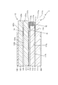
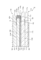
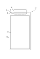
- 1 is a cross-sectional view of the liquid crystal display device shown in FIG. Sectional view enlarging the edge of the panel composite LCD panel top view Sectional drawing which expanded the edge part of the panel composite body of Embodiment 2.
- complex of Embodiment 4 is provided.
- Embodiment 1 of the present invention will be described with reference to FIGS. 1 to 4.
- a liquid crystal display device (display device) 10 will be described as an example.
- FIG. 1 is a plan view of the liquid crystal display device 10 of Embodiment 1
- FIG. 2 is a cross-sectional view of the liquid crystal display device 10 shown in FIG. In each figure, an X axis, a Y axis, and a Z axis are shown as necessary.
- the liquid crystal display device 10 has a rectangular appearance.
- FIG. 1 shows a liquid crystal display device 10 as viewed from the display surface side.
- FIG. 2 schematically shows a cross-sectional structure of the liquid crystal display device 10 cut along the short side direction (AA line shown in FIG. 1).
- the liquid crystal display device 10 according to the present embodiment includes the panel composite body 1, a lighting device 13, a bezel 14, and a housing member 15.
- the panel composite 1 includes a liquid crystal panel (main panel) 11 that displays an image on the display surface on the front side, and an image that is arranged on the front side of the liquid crystal panel 11 and displayed on the display surface of the liquid crystal panel 11 to the user.
- a parallax barrier panel (sub-panel) 12 for visualizing as a stereoscopic image (three-dimensional image) is provided.
- the liquid crystal panel 11 and the parallax barrier panel 12 are both substantially rectangular in shape when viewed from the front side (display surface side), and are set to approximately the same size. However, as will be described later, the liquid crystal panel 11 is set slightly larger than the parallax barrier panel 12. Further, the liquid crystal panel 11 and the parallax barrier panel 12 are bonded to each other via an adhesive layer.
- the lighting device 13 is arranged on the back side of the panel complex 1.
- the lighting device 13 is housed in a box-shaped housing member 15, and a panel composite is placed on the periphery of the housing member 15.
- the illuminating device 13 is comprised so that light may be irradiated toward the back side of the panel composite body 1.
- FIG. Note that a frame-like (frame-like) bezel 14 is put on the periphery of the panel composite 1 (see FIG. 1).
- FIG. 3 is an enlarged cross-sectional view of the end portion of the panel composite 1
- FIG. 4 is a plan view of the liquid crystal panel 11.
- the parallax barrier panel 12 is shown on the upper side
- the liquid crystal panel 11 is shown on the lower side.
- the liquid crystal panel 11 mainly includes a liquid crystal layer 113, a frame-shaped seal portion 114 surrounding the liquid crystal layer 113, and a pair of transparent surfaces whose inner surfaces 111 b and 112 b face each other with the liquid crystal layer 113 and the seal portion 114 interposed therebetween.
- One substrate 111 is a thin film transistor (hereinafter TFT) array substrate (first substrate), and the other substrate 112 is a color filter (hereinafter CF) substrate (second substrate).
- TFT thin film transistor
- CF color filter
- the substrate 111 is set to be slightly larger than the substrate 112 (see FIG. 4). That is, of the pair of substrates 111 and 112, the substrate 111 is large and the substrate 112 is small. Then, as shown in FIG. 3 and the like, the substrates 111 and 112 are bonded to each other so that the end 111a of the substrate 111 protrudes outside the end 112a of the substrate 112. That is, the end of the liquid crystal panel 11 has a stepped shape due to the end 111 a of the substrate 111 and the end 112 a of the substrate 112.
- the end portions 111 a and 112 a of the substrates 111 and 112 are both set to protrude outward from the seal portion 114.
- the thickness of each of the substrates 111 and 112 is set to about 0.25 mm.
- a polarizing plate 115 is attached on the outer surface 112 c of the substrate 112, and a polarizing plate 116 is attached on the outer surface 111 c of the substrate 111.
- the external shape of the polarizing plate 115 is rectangular as shown in FIG.
- the size of the polarizing plate 115 is set to be slightly smaller than the substrate 112.
- the polarizing plate 115 is affixed on the surface 112c so that the periphery may be settled in the surface (front plate
- the thickness of the polarizing plate 115 of this embodiment is set to about 0.12 mm.
- the polarizing plate 115 is made of, for example, a film-like polarizer sandwiched between protective films made of triacetyl cellulose or the like.
- the polarizer is made of, for example, a uniaxially stretched film made of polyvinyl alcohol dyed with iodine.
- another film such as a retardation film may be laminated on the polarizing plate 115.
- the outer shape of the polarizing plate 116 is rectangular, and the size thereof is set to be the same as that of the polarizing plate 115.
- the size of the polarizing plate 116 is set to be slightly smaller than the substrate 111.
- the polarizing plate 116 is also affixed on the surface 111c so that the periphery thereof is within the surface (front plate surface) 111c of the substrate 111. Note that the polarizing plate 116 and the polarizing plate 115 are set to face each other. Note that the polarizing plate 116 also basically has the same structure as the polarizing plate 115.
- a terminal pattern 16 is formed on the inner surface of the end portion of the TFT array substrate 111 to connect to the end portion of the wiring drawn to the outside of the seal portion 114. ing.
- An IC (Integrated Circuit) chip 17 and an FPC (Flexible Printed Circuits) 18 are mounted so as to be electrically connected to the terminal pattern 16.
- the parallax barrier panel 12 mainly includes a liquid crystal layer 123, a frame-shaped seal portion 124 surrounding the liquid crystal layer 123, and a pair of inner surfaces 121b and 122b facing each other across the liquid crystal layer 123 and the seal portion 124.
- the substrate (third substrate) 121 and the substrate (fourth substrate) 122 are both rectangular and have the same size.
- the end 121a of the substrate 121 and the end 122a of the substrate 122 are aligned so as to be at the same position.
- An adhesive layer 21 is disposed between the liquid crystal panel 11 and the parallax barrier panel 12.
- the liquid crystal panel 11 and the parallax barrier panel 12 are bonded to each other with the adhesive layer 21 being stacked therebetween.
- the adhesive layer 21 is made of, for example, a photocurable adhesive mainly composed of a photocurable (photosensitive) resin such as an ultraviolet curable resin.
- the positional relationship between the liquid crystal panel 11 and the parallax barrier panel 12 stacked via the liquid crystal layer 21 is set so that the positions of the seal portions 114 and 124 coincide with each other in the stacking direction, as shown in FIG. ing.
- the end portions 121 a and 122 a of the substrates 121 and 122 of the parallax barrier panel 12 protrude beyond the end of the CF substrate 112 a of the liquid crystal panel 11.
- the outer surface 121 c at the end 121 a of the substrate 121 faces the inner surface 111 b at the end 111 a of the TFT array substrate 111.
- the inner surface 122b of the end portion 122a of the substrate 122 is also opposed to the inner surface 111b through the substrate 121.
- the periphery of the polarizing plate 115 is surrounded between the CF substrate 112 of the liquid crystal panel 11 and the substrate 121 of the parallax barrier panel 12.
- a gap S1 is formed.
- a gap S ⁇ b> 2 that surrounds the periphery of the CF substrate 112 is also formed between the TFT array substrate 111 of the liquid crystal panel 11 and the substrate 121.
- the gap S2 is arranged outside the S1 so as to surround the gap S1, and is connected to the S1. Further, the width of the gap S2 in the stacking direction is larger than the width of the gap 1 in the stacking direction.
- the adhesive layer 21 is mainly disposed between the polarizing plate 115 of the liquid crystal panel 11 and the substrate 121 of the parallax barrier panel 12. That is, the adhesive layer 21 is formed so as to cover the plate surface of the polarizing plate 115. The thickness of the adhesive layer 21 in this portion is about 0.05 mm. Further, a part of the adhesive layer 21 is filled in the gap S ⁇ b> 1 so as to surround the periphery of the polarizing plate 115 placed on the outer surface 112 c of the CF substrate 112. A part of the adhesive layer 21 partially enters the gap S2 described above. However, the adhesive layer 21 protrudes outside from the gap S1 and does not reach the outer surface 122c side of the substrate 122 of the parallax barrier panel 11 or the outer surface 111c side of the TFF array substrate 111 of the liquid crystal panel 11.
- Such an adhesive layer 21 has a function of adhering the liquid crystal panel 11 and the parallax barrier panel 12 and integrating them as one panel composite 1.
- the adhesive layer 21 has a function of protecting the polarizing plate 115 from being swollen (expanded) by absorbing moisture (humidity) in the outside air by covering the periphery of the polarizing plate 115. Note that the polarizing plate 115 is sealed between the CF substrate 112 and the substrate 121 by the adhesive layer 21.
- the manufacturing method of the panel composite 1 provided with the said adhesive layer 21 is demonstrated. First, a predetermined amount of uncured liquid light (ultraviolet) curable adhesive is applied on the plate surface of the polarizing plate 115 provided in the liquid crystal panel 11 (applying step).
- a predetermined amount of uncured liquid light (ultraviolet) curable adhesive is applied on the plate surface of the polarizing plate 115 provided in the liquid crystal panel 11 (applying step).
- a known adhesive applying method is applied. For example, as shown in FIG. 4, the predetermined discharge nozzle (not shown) disposed above the plate surface of the rectangular polarizing plate 115 is moved along the short side direction while moving the predetermined discharge nozzle (not shown).
- a plurality of linear coating films R made of the adhesive may be formed on the plate surface by discharging the adhesive from a discharge nozzle.
- the coating film R is formed entirely on the plate surface of the polarizing plate 115.
- a portion (gap) where the coating R is not formed is formed between the adjacent linear coating films R. It may be.
- the coating film R finally spreads uniformly on the plate surface of the polarizing plate 115 and becomes an adhesive layer covering the entire plate surface.
- the parallax barrier panel 12 is placed on the coating film R (lamination process).
- the parallax barrier panel 12 is placed on the coating R so that the substrate 121 is in direct contact with the coating R. That is, the coating film R made of the adhesive is sandwiched between the plate surface of the polarizing plate 115 and the outer surface 121 c of the substrate 121.
- the parallax barrier panel 12 is pressed against the plate surface of the polarizing plate 115 with a certain amount of force. Then, the coating film R made of the adhesive is sandwiched between the plate surface of the polarizing plate 115 and the outer surface 121 c of the substrate 121 and crushed, and is thinly spread so as to cover the plate surface of the polarizing plate 115. At this time, the coating film R formed on the plate surface on the peripheral side of the polarizing plate 115 protrudes outward from the peripheral edge of the polarizing plate 15. In FIG. 4, a state in which a part of the coating film R protrudes outward from the periphery of the polarizing plate 115 is schematically shown using arrows.
- a part of the adhesive forming the coating film R enters the gap S1 shown in FIG. Then, the periphery of the polarizing plate 115 is covered with the adhesive. Note that a part of the adhesive that has entered the gap S ⁇ b> 1 may enter the gap S ⁇ b> 2 beyond the end 112 a of the CF substrate 112. The arrangement relationship between the liquid crystal panel 11 and the parallax barrier panel 12 is appropriately adjusted in a state where the adhesive is uncured.
- the adhesive is cured by irradiating the adhesive with ultraviolet rays (curing step).
- an adhesive layer 21 as shown in FIG. 3 is formed, and the liquid crystal panel 11 and the parallax barrier panel 12 are bonded. Further, the peripheral edge of the polarizing plate 115 is sealed with the adhesive layer 21.
- light such as an ultraviolet-ray, is irradiated toward the said adhesive agent so that they may penetrate from the outside of each panel 11 and 12, for example. As described above, the liquid crystal panel 11 and the parallax barrier panel 12 are bonded together to obtain the panel composite 1.
- the adhesive does not reach every corner on the plate surface, and the liquid crystal panel 11 and the parallax barrier panel 12 Adhesion of is insufficient. Even if the liquid crystal panel 11 and the parallax barrier panel 12 are sufficiently bonded, the periphery of the polarizing plate 115 may be exposed depending on the total amount of the adhesive applied. That is, depending on the total amount of the applied adhesive, the amount of the adhesive that protrudes outside between the polarizing plate 115 and the substrate 121 may be insufficient.
- the total amount of the adhesive applied on the plate surface of the polarizing plate 115 is protruded from the end of the panel composite 1. It is set a little more in a range that is not.
- the gap S1 accommodates the adhesive for covering the periphery of the polarizing plate 115 between the CF substrate 112 of the liquid crystal panel 11 and the substrate 121 of the parallax barrier panel 12.
- a gap S2 that can accommodate the adhesive protruding from the gap S1.
- it is easy to set a large amount in advance on the plate surface of the polarizing plate 115. That is, the allowable range of the total amount of the adhesive applied on the plate surface of the polarizing plate 115 is widened by providing the gap S2. Therefore, even if the use environment (humidity, temperature, etc.) of the adhesive changes and the concentration, viscosity, etc. of the adhesive change, it is easy to control the applied amount of the adhesive.
- the front side of the parallax barrier panel 12 (the outer surface 122c side of the substrate 122) and the back side of the liquid crystal panel 11 (the outer surface 111c side of the TFT array substrate 11).
- the liquid crystal panel 11 and the parallax barrier panel 12 can be satisfactorily bonded to each other while the liquid adhesive wraps around, adheres to the surfaces thereof, and is prevented from being contaminated. That is, according to the panel composite body and the manufacturing method thereof of the present embodiment, the liquid crystal panel 11 and the parallax barrier panel 12 are sufficiently bonded while the contamination as described above is suppressed, and around the polarizing plate 115.
- the adhesive can be spread so that no gap is formed.
- FIG. 5 is an enlarged cross-sectional view of an end portion of the panel composite body 1A according to the second embodiment.
- the basic configuration of the panel complex 1A of the present embodiment is the same as that of the first embodiment.
- the liquid crystal panel 11 is the same as that of the first embodiment.
- the basic configuration of the parallax barrier panel 12A is the same as that of the first embodiment.
- the substrate 121A provided in the parallax barrier panel 12A is smaller (small) than the one in the first embodiment, and the end 122a is inside (the seal portion 124 side) from the one in the first embodiment. It is arranged in.
- the end 122a of the substrate 122 of the parallax barrier panel 12A protrudes outside the end 121Aa of the substrate 121A, and the inner surface 122b of the end 122a has a TFT array substrate 111 provided in the liquid crystal panel 11. It faces the inner surface 111b at the end 111a. That is, the end portion of the parallax barrier panel 12 has a stepped shape, similarly to the end portion of the liquid crystal panel 11.
- the position of the end 121Aa of the substrate 121A provided in the parallax barrier panel 12A is aligned with the position of the end 112a of the CF substrate 112 provided in the liquid crystal panel 11.
- a gap S1A is formed between the outer surface 112c of the substrate 112 and the outer surface 121Ac of the substrate 121A so as to surround the periphery of the polarizing plate 151. Further, a gap S ⁇ b> 2 ⁇ / b> A is also formed between the inner surface 111 b of the substrate 111 and the inner surface 122 b of the substrate 122.
- the width of the gap S2A in the stacking direction is larger than the width of the gap S2 of the first embodiment, and the adhesive 21A that protrudes outward from between the substrate 112 and the substrate 121 is removed. The amount that can be accommodated is larger than the gap S2 of the first embodiment.
- the allowable range of the total amount of the adhesive applied on the plate surface of the polarizing plate 115 is the first embodiment. It is wider than the case.
- the liquid adhesive flows around the front side of the parallax barrier panel 12A (the outer surface 122c side of the substrate 122) and the back side of the liquid crystal panel 11 (the outer surface 111c side of the TFT array substrate 111).
- the liquid crystal panel 11 and the parallax barrier panel 12A can be bonded together while being suppressed from adhering to and contaminating those surfaces. That is, according to the panel composite body 1A and the manufacturing method thereof according to the present embodiment, the liquid crystal panel 11 and the parallax barrier panel 12A are sufficiently bonded while the above-described contamination is suppressed, and around the polarizing plate 115.
- the adhesive can be spread so that no gap is formed.
- FIG. 6 is an enlarged cross-sectional view of an end portion of the panel composite body 1B according to the third embodiment.
- the liquid crystal panel 11 provided in the panel complex 1B of the present embodiment is the same as that of the first embodiment.
- a single protective plate 122B is attached to the liquid crystal panel 11 instead of the sub panel.
- the protective plate 122B is for protecting the display surface of the liquid crystal panel 11, and is made of a transparent plate-like member.
- the protective plate 122B has a rectangular external appearance, and its end 122Ba is set so as to protrude outward from the end 112a of the CF substrate 112 of the liquid crystal panel 11.
- the inner surface 122Bb at the end 122Ba faces the inner surface 111b at the end 111a of the TFT array substrate 111.
- the inner surface 122Bb of the protection plate 122B is also opposed to the outer surface 112c of the CF substrate 112.
- a gap S1B is formed between the outer surface 112c of the substrate 112 and the inner surface 122Bb of the protective plate 122B so as to surround the periphery of the polarizing plate 151. Further, a gap S2B is also formed between the inner surface 111b of the substrate 111 and the inner surface 122Bb of the substrate 122B.
- the liquid crystal panel 11 and the protection plate 122B are bonded to each other by the adhesive layer 21B.
- the object bonded to the liquid crystal panel 11 is not a panel in which a plurality of substrates (plates) as in the first embodiment or the like is laminated, but may be a single protective plate 122B.
- the liquid adhesive wraps around the front side (outer surface 122Bc side) of the protective plate 122B and the back side of the liquid crystal panel 11 (outside surface 111c side of the TFT array substrate 111) and adheres to those surfaces.
- the liquid crystal panel 11 and the protective plate 122B can be bonded together while being prevented from being contaminated. That is, according to the panel composite body 1B and the manufacturing method thereof according to the present embodiment, the liquid crystal panel 11 and the protective plate 122B are sufficiently bonded and the periphery of the polarizing plate 115 is bonded while the above contamination is suppressed. The agent can be distributed so that no gaps are formed.
- FIG. 7 is an enlarged cross-sectional view of an end portion of the panel composite body 1C of the fourth embodiment
- FIG. 8 is a plan view of the liquid crystal panel 1C included in the panel composite body 1C of the fourth embodiment.
- the parallax barrier panel 12 provided in the panel complex 1C of the present embodiment is the same as that of the second embodiment.
- the basic configuration of the liquid crystal panel 1C is the same as that of the second embodiment and the like, but the CF substrate 112C is set larger (smaller) than that of the second embodiment. .
- the position of the end 112Ca of the CF substrate 112C is aligned with the position of the end 111a of the TFT array substrate 111.
- the length in the long side direction of the TFT array substrate 111 is set longer than the length in the long side direction of the CF substrate 112C, and the IC chip 16 and the like are mounted. A portion is exposed from the CF substrate 112C.
- the length in the short side direction of the TFT array substrate 111 is set to be the same as the length in the short side direction of the CF substrate 112C.
- the inner surface 122b of the end 122a of the substrate 122 is opposed to the outer surface 122Cc of the end 112Ca of the CF substrate 112C.
- the end 121Aa of the end 121A of the substrate 121A is arranged on the inner side of the end 122a of the substrate 122, the outer surface 121Ac faces the outer surface 122Cc of the CF substrate 112C, like the substrate 122. is doing.
- a gap S1C is formed between the outer surface 112Cc of the substrate 112C and the outer surface 121Ac of the substrate 121A, and a gap S2C is formed between the outer surface 112Cc of the substrate 112C and the inner surface 122a of the substrate 122.
- the liquid crystal panel 11C and the parallax barrier panel 12A are bonded to each other by an adhesive layer 21C.
- the gaps S1C and S2C as described above may be formed by making the end portion of the parallax barrier panel 12A as a sub-panel instead of the liquid crystal panel 11 as a main panel stepped.
- the liquid adhesive wraps around the front side (outer surface 122c side) of the parallax barrier panel 12A and the back side of the liquid crystal panel 11C (outside surface 111c side of the TFT array substrate 111), and the surfaces thereof.
- the liquid crystal panel 11 ⁇ / b> C and the parallax barrier panel 12 ⁇ / b> A can be bonded together while being prevented from adhering to and contaminating. That is, according to the panel composite body 1C and the manufacturing method thereof of the present embodiment, the liquid crystal panel 11C and the parallax barrier panel 12A are sufficiently bonded and the surroundings of the polarizing plate 115 while suppressing the contamination as described above.
- the adhesive can be spread so that no gap is formed.
- the object to be bonded to the liquid crystal panel as the main panel is a parallax barrier panel or a protective plate as a sub panel, but in other embodiments, other than these It may be.
- the sub panel includes various panels such as a viewing angle control panel, a touch panel, and other panels for image display, and is not particularly limited.
- the sub-panel (parallax barrier panel) has a configuration in which one polarizing plate is attached to one outer side (display surface side).
- a configuration in which a pair of polarizing plates is attached to both outer sides of the sub panel may be employed.
- the photocurable adhesive is hardened by ultraviolet rays, but in other embodiments, it may be hardened by other light such as visible light and infrared light. .
- the adhesive is mainly composed of a photocurable resin.
- the adhesive may be composed mainly of a thermosetting resin. .
- the panel composite has a configuration in which one sub panel is laminated on one main panel via an adhesive layer.
- the structure may be such that two or more sub-panels are laminated on each main panel via an adhesive layer.
- one sub panel is laminated on one main panel via an adhesive layer, and a plate member such as a protective plate is laminated on the sub panel via another adhesive layer. It may be.
- the main panel included in the panel composite is set slightly larger than the sub panel.
- the main panel and the sub panel may be set to the same size, or the sub panel may be set larger than the main panel.
- SYMBOLS 1,1A, 1B, 1C ... Panel complex 10 ... Liquid crystal display device (display device), 11, 11A, 11C ... Liquid crystal panel (main panel), 12, 12A ... Parallax barrier panel (sub panel), 21, 21A, 21B, 21C ... Adhesive layer, 111 ... TFT array substrate (first substrate), 112 ... CF substrate (second substrate), 113 ... Liquid crystal layer, 115 ... Polarizing plate, 121 ... Substrate (third substrate, counter plate) Member), 122 ... substrate (fourth substrate, plate member), 123 ... liquid crystal layer, S1, S1A, S1B, S1C ... gap, S2, S2A, S2B, S2C ... gap
Landscapes
- Physics & Mathematics (AREA)
- Nonlinear Science (AREA)
- Mathematical Physics (AREA)
- Chemical & Material Sciences (AREA)
- Crystallography & Structural Chemistry (AREA)
- General Physics & Mathematics (AREA)
- Optics & Photonics (AREA)
- Liquid Crystal (AREA)
Abstract
本発明に係るパネル複合体1は、大判の基板111の端部111aが小判の基板112の端部112aよりも外側にはみ出してなる大判の第1基板111及び小判の第2基板112と、第2基板112の板面内に収まるように第2基板の外面112c側に配される偏光板115とを有する主パネル11と、第2基板112の端部112aよりも外側にはみ出すと共に、第2基板112との間で偏光板115を挟む板部材12と、偏光板115と板部材12との間に配されると共に、偏光板115の周縁を覆うように第2基板112と板部材12との間に配されて、主パネル11と板部材12とを接着する接着層21とを備える。
Description
本発明は、パネル複合体、表示装置及びパネル複合体の製造方法に関する。
近年、画像等を表示させる液晶パネルと共に、タッチパネル、視野角制御用パネル、視差バリア用パネル等の機能パネルを備えた表示装置が知られている(例えば、特許文献1参照)。この種の表示装置では、主パネルとしての前記液晶パネルの表面上に、副パネルとしての前記機能パネルが接着剤を介して貼り付けられている。
なお、前記接着剤としては、一般的に、光硬化性(感光性)接着剤が利用されている。この光硬化性接着剤は、紫外線等の光が照射されて硬化される前は液状であり、流動性を備えている。主パネルと副パネルとを貼り合わせる際は、この流動性を備えた状態の前記接着剤が、先ず主パネルの表面上に付与される。そしてこの付与された前記接着剤を挟むように、主パネルの表面上に副パネルが重ねられる。その後、主パネル及び副パネルがそれぞれ位置決めされ、更に前記接着剤に対して紫外線等の光が照射されて、主パネルと副パネルとが接着される。
主パネルと副パネルとの間に介在される接着剤の層の厚みが不均一であると、主パネルと副パネルとの距離(間隔)にばらつきが生じてしまう。すると、副パネルを通してユーザに視認される主パネルの画像に、色ムラ等の表示ムラが発生することがある。そのため、前記接着剤の層の厚みが均一となるように、前記接着剤は、流動性を備えている状態で、主パネルと副パネルとの間で挟まれて平坦になるように薄く拡げられている。
なお、主パネル(液晶パネル)の最表面には、通常、偏光板が備えられている。そのため、具体的には、この偏光板と前記副パネルとの間で、前記接着剤が上記のように薄く拡げられている。偏光板は、通常、主パネル(液晶パネル)の本体部分よりも一回り小さいく設定されているため、偏光板の周縁は、主パネルの周縁よりも内側に引っ込んだ形となっている。
ところで、前記接着剤の中には、前記偏光板と副パネルとの間から外側にはみ出すものもある。外側にはみ出したものの一部は、前記偏光板の周縁よりも外側にある前記主パネルの本体部分の表面上にまで至り、前記偏光板の周縁を覆うことになる。
偏光板は、湿度の影響を受け易く、外気中の水分(湿気)を吸収すると膨潤するため、その厚みが変化することがある。すると、膨潤した前記偏光板が上記のような表示ムラの原因となることがある。そのため、偏光板の周縁は前記接着剤によって覆われている。
(発明が解決しようとする課題)
主パネルと副パネルとの間から、上記のように液状の接着剤が外側にはみ出すと、はみ出す分量によっては、副パネルの表示面側或いは主パネルの背面側にまで前記接着剤が回り込んでしまうことがあり、問題となっている。前記接着剤が副パネルの表示面側等に付着すると、その付着した部分が汚れてしまい、表示不良の原因となっている。
主パネルと副パネルとの間から、上記のように液状の接着剤が外側にはみ出すと、はみ出す分量によっては、副パネルの表示面側或いは主パネルの背面側にまで前記接着剤が回り込んでしまうことがあり、問題となっている。前記接着剤が副パネルの表示面側等に付着すると、その付着した部分が汚れてしまい、表示不良の原因となっている。
本発明の目的は、主パネルとそれに貼り付けられる対象物とを備えるパネル複合体において、それらの間に配されている接着剤がパネル複合体の端部から外側にはみ出すことを抑制する技術を提供することである。
(課題を解決するための手段)
本発明に係るパネル複合体は、互いの内面が対向するように貼り合わされた大小一対の基板であって大判の基板の端部が小判の基板の端部よりも外側にはみ出してなる大判の第1基板及び小判の第2基板と、前記第2基板の板面内に収まるように前記第2基板の外面側に配される偏光板とを有する主パネルと、前記第2基板の端部よりも外側にはみ出すと共に、前記第2基板との間で前記偏光板を挟む板部材と、前記偏光板と前記板部材との間に配されると共に、前記偏光板の周縁を覆うように前記第2基板と前記板部材との間に配されて、前記主パネルと前記板部材とを接着する接着層とを備える。
本発明に係るパネル複合体は、互いの内面が対向するように貼り合わされた大小一対の基板であって大判の基板の端部が小判の基板の端部よりも外側にはみ出してなる大判の第1基板及び小判の第2基板と、前記第2基板の板面内に収まるように前記第2基板の外面側に配される偏光板とを有する主パネルと、前記第2基板の端部よりも外側にはみ出すと共に、前記第2基板との間で前記偏光板を挟む板部材と、前記偏光板と前記板部材との間に配されると共に、前記偏光板の周縁を覆うように前記第2基板と前記板部材との間に配されて、前記主パネルと前記板部材とを接着する接着層とを備える。
前記パネル複合体において、前記板部材と、前記板部材と対向するように貼り合わされると共に前記板部材と前記偏光板との間に配される対向板部材とを有する副パネルを更に備えてもよい。
前記パネル複合体において、前記副パネルが、互いの内面が対向するように貼り合わされた大小一対の基板であって大判の基板の端部が小判の基板の端部よりも外側にはみ出した前記対向板部材としての小判の第3基板及び前記板部材としての大判の第4基板とを有し、少なくとも前記第4基板の端部が前記第2基板の端部よりも外側にはみ出して前記第4基板の端部における内面と、前記第1基板の端部における内面とが対向すると共に、前記第3基板が前記第2基板との間で前記偏光板を挟み、前記接着層が、前記偏光板と前記第3基板との間に配されると共に、前記偏光板の周縁を覆うように前記第2基板と前記第3基板との間に配されて、前記主パネルと前記副パネルとを接着してもよい。
本発明に係る他のパネル複合体は、互いの内面が対向するように貼り合わされた一対の第1基板及び第2基板と、前記第2基板の板面内に収まるように前記第2基板の外面側に配される偏光板とを有する主パネルと、互いの内面が対向するように貼り合わされた大小一対の基板であって大判の基板の端部が小判の基板の端部よりも外側にはみ出してなる小判の第3基板及び大判の第4基板とを有し、前記第4基板の端部における内面と前記第2基板の端部における外面とが対向すると共に、前記第3基板が前記第2基板との間で前記偏光板を挟む副パネルと、前記偏光板と前記第3基板との間に配されると共に、前記偏光板の周縁を覆うように前記第2基板と前記第3基板との間に配されて、前記主パネルと前記副パネルとを接着する接着層とを備える。
前記パネル複合体において、前記接着層が、光硬化性接着剤からなることが好ましい。
本発明に係る表示装置は、前記パネル複合体と、前記パネル複合体に光を照射する照明装置とを備える。
本発明に係るパネル複合体の製造方法は、互いの内面が対向するように貼り合わされた大小一対の基板であって大判の基板の端部が小判の端部よりも外側にはみ出してなる大判の第1基板及び小判の第2基板と、前記第2基板の板面内に収まるように前記第2基板の外面側に配される偏光板とを有する主パネルの前記偏光板における板面上に、硬化前の流動性を備えた光硬化性接着剤を付与する付与工程と、板部材を、前記第2基板の端部よりも外側にはみ出すと共に、前記第2基板との間で前記偏光板を挟むように、前記接着剤が付与された前記偏光板の板面上に重ねると共に、前記板部材と前記偏光板との間で前記接着剤を挟んで押し広げる積層工程と、前記接着剤に光を照射して前記接着剤を硬化させて前記主パネルと前記板部材とを接着する硬化工程とを備える。
前記パネル複合体の製造方法において、前記板部材と、前記板部材と対向するように貼り合わされると共に前記板部材と前記偏光板との間に配される対向板部材とを有する副パネルを更に備えてもよい。
前記パネル複合体の製造方法において、前記副パネルが、互いの内面が対向するように貼り合わされた大小一対の基板であって大判の基板の端部が小判の基板の端部よりも外側にはみ出した前記対向板部材としての小判の第3基板及び前記板部材としての大判の第4基板とを有し、前記積層工程において、少なくとも前記第4基板の端部が前記第2基板の端部よりも外側にはみ出して前記第4基板の端部における内面と、前記第1基板の端部における内面とが対向すると共に、前記第3基板が前記第2基板との間で前記偏光板を挟むように、前記副パネルを、前記接着剤が付与された前記偏光板の板面上に重ねると共に、前記副パネルと前記偏光板との間で前記接着剤を挟んで押し広げ、前記硬化工程において、前記接着剤に光を照射して前記接着剤を硬化させて前記主パネルと前記副パネルとを接着してもよい。
本発明の他のパネル複合体の製造方法は、互いの内面が対向するように貼り合わされた一対の第1基板及び第2基板と、前記第2基板の板面内に収まるように前記第2基板の外面側に配される偏光板とを有する主パネルの前記偏光板における板面上に、硬化前の流動性を備えた光硬化性接着剤を付与する付与工程と、互いの内面が対向するように貼り合わされた大小一対の基板であって大判の基板の端部が小判の基板の端部よりも外側にはみ出してなる小判の第3基板及び大判の第4基板とを有する副パネルを、前記第4基板の端部における内面と前記第2基板の端部における外面とが対向すると共に、前記第3基板が前記第2基板との間で前記偏光板を挟むように、前記接着剤が付与された前記偏光板の板面上に重ねると共に、前記副パネルと前記偏光板との間で前記接着剤を挟んで押し広げる積層工程と、前記接着剤に光を照射して前記接着剤を硬化させて前記主パネルと前記副パネルとを接着する硬化工程とを備える。
(発明の効果)
本発明によれば、主パネルとそれに貼り付けられる対象物とを備えるパネル複合体において、それらの間に配されている接着剤がパネル複合体の端部から外側にはみ出すことを抑制する技術を提供できる。
本発明によれば、主パネルとそれに貼り付けられる対象物とを備えるパネル複合体において、それらの間に配されている接着剤がパネル複合体の端部から外側にはみ出すことを抑制する技術を提供できる。
<実施形態1>
本発明の実施形態1を、図1ないし図4を参照しつつ説明する。本実施形態では、液晶表示装置(表示装置)10を例に挙げて説明する。図1は、実施形態1の液晶表示装置10の平面図であり、図2は、図1に示される液晶表示装置10の断面図である。なお、各図には、必要に応じて、X軸、Y軸及びZ軸が示されている。
本発明の実施形態1を、図1ないし図4を参照しつつ説明する。本実施形態では、液晶表示装置(表示装置)10を例に挙げて説明する。図1は、実施形態1の液晶表示装置10の平面図であり、図2は、図1に示される液晶表示装置10の断面図である。なお、各図には、必要に応じて、X軸、Y軸及びZ軸が示されている。
(液晶表示装置)
液晶表示装置10は、図1に示されるように、その外観形状が矩形状となっている。図1には、表示面側から見た状態の液晶表示装置10が示されている。そして、図2には、短辺方向(図1に示されるA-A直線)に沿って切断された液晶表示装置10の断面構造が模式的に示されている。本実施形態の液晶表示装置10は、図2に示されるように、パネル複合体1と、照明装置13と、ベゼル14と、収容部材15とを備える。
液晶表示装置10は、図1に示されるように、その外観形状が矩形状となっている。図1には、表示面側から見た状態の液晶表示装置10が示されている。そして、図2には、短辺方向(図1に示されるA-A直線)に沿って切断された液晶表示装置10の断面構造が模式的に示されている。本実施形態の液晶表示装置10は、図2に示されるように、パネル複合体1と、照明装置13と、ベゼル14と、収容部材15とを備える。
パネル複合体1は、表側にある表示面に画像を表示させる液晶パネル(主パネル)11と、液晶パネル11の表側に配されて、液晶パネル11の表示面に表示される画像を、ユーザに立体画像(三次元画像)として視認させるための視差バリア用パネル(副パネル)12とを備える。液晶パネル11と、視差バリア用パネル12とは、共に表側(表示面側)から見た状態が概ね矩形状であり、概ね同じ大きさに設定されている。ただし、後述するように、液晶パネル11の方が、視差バリア用パネル12よりも若干、大きく設定されている。また、液晶パネル11と、視差バリア用パネル12とは、互いに接着層を介して貼り合わされている。
パネル複合体1の背面側には、照明装置13が配されている。照明装置13は、箱状の収容部材15内に収容されており、その収容部材15の周縁上にパネル複合体が載せられている。そして、照明装置13は、パネル複合体1の背面側に向けて光を照射するように構成されている。なお、パネル複合体1の周縁には、額縁状(枠状)のベゼル14が被せられている(図1参照)。
ここで、図3及び図4を参照しつつ、パネル複合体1及びこれらを構成する各パネル11,12について詳細に説明する。図3は、パネル複合体1の端部を拡大した断面図であり、図4は液晶パネル11の平面図である。図3において、上側に視差バリア用パネル12が示され、下側に液晶パネル11が示されている。
液晶パネル11は、主として、液晶層113と、この液晶層113の周りを囲む枠状のシール部114と、液晶層113及びシール部114を挟んで互いの内面111b,112bが対向する一対の透明な基板111,112とを備えている。一方の基板111は、薄膜トランジスタ(以下、TFT)アレイ基板(第1基板)であり、他方の基板112は、カラーフィルタ(以下、CF)基板(第2基板)である。
基板111と基板112とは共に外観形状が矩形状であるものの、基板111の方が基板112よりも一回り大きく設定されている(図4参照)。つまり、前記一対の基板111,112のうち、基板111が大判であり、基板112が小判となっている。そして、図3等に示されるように、基板111の端部111aが、基板112の端部112aよりも外側にはみ出すように(張り出すように)、基板111,112同士が貼り合わされている。つまり、液晶パネル11の端部は、基板111の端部111aと、基板112の端部112aとによって段差状になっている。なお、各基板111,112の端部111a,112aは、共にシール部114よりも外側にはみ出すように設定されている。本実施形態における各基板111,112の厚みは、それぞれ0.25mm程度に設定されている。
図3に示されるように、基板112の外面112c上には、偏光板115が貼り付けられており、また基板111の外面111c上には偏光板116が貼り付けられている。偏光板115の外観形状は、図4に示されるように矩形状である。偏光板115の大きさは、基板112よりも一回り程度小さく設定されている。そして、偏光板115は、その周縁が、基板112の表面(表側の板面)112c内に収まるように、その表面112c上に貼り付けられている。本実施形態の偏光板115の厚みは、0.12mm程度に設定されている。
なお偏光板115は、例えば、フィルム状の偏光子をトリアセチルセルロース等からなる保護フィルムで挟んだものからなる。前記偏光子は、例えば、ヨウ素で染色されたポリビニルアルコール製のフィルムが一軸延伸加工されたものからなる。また、他の実施形態においては、偏光板115に、位相差フィルム等の他のフィルムが積層されていてもよい。
偏光板116は、偏光板115と同様、その外観形状は矩形状であり、その大きさも偏光板115と同じに設定されている。そして偏光板116の大きさは、基板111よりも一回り程度小さく設定されている。また、偏光板116についても、その周縁が基板111の表面(表側の板面)111c内に収まるように、その表面111c上に貼り付けられている。なお、偏光板116と、偏光板115とは対向するように設定されている。なお、偏光板116も、基本的には偏光板115と同様な構造からなる。
なお、液晶パネル11は、図4に示されるように、TFTアレイ基板111の端部の内面上には、シール部114の外側に引き出された配線の端部と接続する端子パターン16が形成されている。そして、その端子パターン16と電気的に接続するようにIC(Integrated Circuit)チップ17及びFPC(Flexible Printed Circuits)18が実装されている。
視差バリア用パネル12は、主として、液晶層123と、この液晶層123の周りを囲む枠状のシール部124と、液晶層123及びシール部124を挟んで互いの内面121b,122bが対向する一対の透明な基板121,122とを備えている。基板(第3基板)121及び基板(第4基板)122は、共に矩形状であり、同じ大きさに設定されている。そして、基板121の端部121aと、基板122の端部122aとは同じ位置になるように揃えられている。
液晶パネル11と視差バリア用パネル12との間には、接着層21が配されている。そして、液晶パネル11と視差バリア用パネル12とは、この接着層21を介して互いに積層された状態で接着されている。この接着層21は、例えば、紫外線硬化樹脂等の光硬化性(感光性)樹脂を主成分とする光硬化性接着剤からなる。
液晶層21を介して積層された液晶パネル11及び視差バリア用パネル12の配置関係は、図3に示されるように、互いのシール部114,124の位置が積層方向において一致するように設定されている。そしてこの状態において、視差バリア用パネル12の各基板121,122の各端部121a,122aは、液晶パネル11のCF基板112aの端部よりも外側にはみ出している。また、基板121の端部121aにおける外面121cは、TFTアレイ基板111の端部111aにおける内面111bと対向している。なお、基板122の端部122aにおける内面122bも、基板121越しに、前記内面111bと対向している。
液晶パネル11と、視差バリア用パネル12とがこのような配置関係にあると、液晶パネル11のCF基板112と、視差バリア用パネル12の基板121との間に、偏光板115の周縁を取り囲むような隙間S1が形成される。また、液晶パネル11のTFTアレイ基板111と、前記基板121との間にも、CF基板112の周縁を取り囲むような隙間S2が形成される。隙間S2は、隙間S1を取り囲むように前記S1よりも外側に配されており、前記S1と繋がっている。また、隙間S2の積層方向における幅は、隙間1の積層方向における幅と比べて大きくなっている。
また、図3に示されるように、接着層21は、主として、液晶パネル11の偏光板115と、視差バリア用パネル12の基板121との間に配されている。つまり、接着層21は、偏光板115の板面を覆うように形成されている。この部分における接着層21の厚みは、0.05mm程度である。また、接着層21の一部は、CF基板112の外面112c上に載せられている偏光板115の周縁を取り囲むように、前記隙間S1に充填されている。なお、上述した前記隙間S2にも、部分的に接着層21の一部が入り込んでいる。ただし、接着層21は、前記隙間S1から外部にはみ出して、視差バリア用パネル11の基板122の外面122c側、或いは液晶パネル11のTFFアレイ基板111の外面111c側にまでは及んでいない。
このような接着層21は、液晶パネル11と視差バリア用パネル12とを接着して、これらを1つのパネル複合体1として一体化する機能を備えている。また、接着層21は、偏光板115の周りを覆うことによって、偏光板115が外気中の水分(湿気)を吸収して膨潤(膨張)しないように保護する機能も備えている。なお、偏光板115は、CF基板112と基板121との間で、接着層21によって封止された状態になっている。
ここで、前記接着層21を備えたパネル複合体1の製造方法を説明する。先ず、液晶パネル11が備えている偏光板115の板面上に、未硬化の液体状の光(紫外線)硬化性接着剤が所定量付与される(付与工程)。
偏光板115の板面上に、前記接着剤を付与する方法としては、公知の接着剤付与方法が適用される。例えば、図4に示されるように、矩形状の偏光板115の板面に対して、その上方に配されている所定の吐出ノズル(不図示)を、短辺方向に沿って移動させながら前記吐出ノズルから前記接着剤を吐出させて前記板面上に前記接着剤からなる線状の塗膜Rを複数本形成してもよい。なお塗膜Rは、偏光板115の板面に対して、全面的に形成される。ただし、偏光板115の板面上に、前記接着剤を付与した段階では、隣り合った線状の塗膜R同士の間には、前記塗Rが形成されていない部分(隙間)が形成されていてもよい。前記塗膜Rは、後述するように、最終的には、偏光板115の板面上で均一に拡がって、前記板面を全面的に覆う接着層となる。
偏光板115の板面上に、前記塗膜Rを形成した後、その塗膜Rの上に、視差バリア用パネル12が載せられる(積層工程)。視差バリア用パネル12は、その基板121が直接、塗膜Rと接触するように、前記塗膜R上に載せられる。つまり、前記接着剤からなる塗膜Rは、偏光板115の板面と、基板121の外面121cとの間で挟まれることになる。
なお、視差バリア用パネル12は、偏光板115の板面に対してある程度の力で押し付けられる。すると、前記接着剤からなる塗膜Rは、偏光板115の板面と、基板121の外面121cとの間で挟まれて押し潰され、偏光板115の板面を覆うように薄く拡げられる。この際、偏光板115の周縁側の板面上に形成されている前記塗膜Rは、偏光板15の周縁から外側にはみ出す。なお、図4におして偏光板115の周縁から外側に前記塗膜Rの一部がはみ出す様子が、矢印を用いて模式的に示されている。すると、図3に示される隙間S1内に、前記塗膜Rを成す前記接着剤の一部が浸入することになる。そして、偏光板115の周りが前記接着剤によって覆われる。なお、隙間S1内に浸入した前記接着剤の一部は、CF基板112の端部112aを越えて、更に隙間S2内に浸入してもよい。なお、液晶パネル11と視差バリア用パネル12との配置関係は、前記接着剤が未硬化の状態で、適宜、調整される。
その後、前記接着剤に対して、紫外線が照射されて、前記接着剤が硬化される(硬化工程)。前記接着剤が硬化すると図3に示されるような接着層21となり、液晶パネル11と視差バリア用パネル12とが接着される。また、偏光板115の周縁が接着層21によって封止される。なお紫外線等の光は、例えば、各パネル11,12の外側からそれらを貫通するように前記接着剤に向けて照射される。以上のようにして、液晶パネル11と視差バリア用パネル12とが貼り合わされて、パネル複合体1が得られる。
ところで、偏光板115の板面上に付与される液状の前記接着剤の総量が少ないと、前記板面上の隅々にまで前記接着剤が行き渡らず、液晶パネル11と視差バリア用パネル12との接着が不十分となる。また、液晶パネル11と視差バリア用パネル12との接着が十分であっても、付与される前記接着剤の総量によっては、偏光板115の周縁が露出してしまうことがある。つまり、付与される前記接着剤の総量によっては、偏光板115と基板121との間から、外側にはみ出す前記接着剤の量が不足することがある。
そのため、偏光板115の周縁を確実に前記接着剤で覆うためには、一般的に、偏光板115の板面上に付与する前記接着剤の総量を、パネル複合体1の端部からはみ出さない範囲で、幾分多めに設定される。
本実施形態の場合、液晶パネル11のCF基板112と、視差バリア用パネル12の基板121との間には、偏光板115の周縁を覆うための前記接着剤を収容する隙間S1があり、更に前記隙間S1の外側には、前記隙間S1からはみ出す前記接着剤を収容できる隙間S2がある。そのため、偏光板115の板面上に、予め付与しておく前記樹脂の総量を、予め多めに設定し易くなっている。つまり、偏光板115の板面上に付与される前記接着剤の総量の許容範囲が、前記隙間S2が設けられていることによって、広くなっている。そのため、接着剤の使用環境(湿度、温度等)が変化して接着剤の濃度、粘度等が変化しても、接着剤の付与量を制御し易い。
したがって、本実施形態のパネル複合体1及びその製造方法によれば、視差バリア用パネル12の表側(基板122の外面122c側)や、液晶パネル11の背面側(TFTアレイ基板11の外面111c側)に、液状の接着剤が回り込んで、それらの表面に付着し、汚染することが抑制されつつ、良好に液晶パネル11と視差バリア用パネル12とを貼り合わせることができる。つまり、本実施形態のパネル複合体及びその製造方法によれば、上記のような汚染が抑制されつつ、液晶パネル11と視差バリア用パネル12との接着を十分行うと共に、偏光板115の周りに接着剤を隙間が形成されないように行き渡らせることができる。
<実施形態2>
次いで、本発明の実施形態2を、図5を参照しつつ説明する。なお、以降の各実施形態では、実施形態1と同じ部分については、実施形態1のものと同じ符号を付して、その詳細な説明は省略する。図5は、実施形態2のパネル複合体1Aの端部を拡大した断面図である。本実施形態のパネル複合体1Aの基本的な構成は、実施形態1のものと同様である。具体的には、液晶パネル11は実施形態1のものと同じである。なお、視差バリア用パネル12Aについても、その基本的な構成は、実施形態1のものと同様である。ただし、視差バリア用パネル12Aが備えている基板121Aが、実施形態1のものよりも小型(小判)になっており、その端部122aが実施形態1のものよりも内側(シール部124側)に配されている。つまり、視差バリア用パネル12Aの基板122の端部122aは、基板121Aの端部121Aaよりも外側にはみ出しており、その端部122aにおける内面122bが、液晶パネル11が備えているTFTアレイ基板111の端部111aにおける内面111bと対向している。つまり、視差バリア用パネル12の端部も、液晶パネル11の端部と同じように、段差状になっている。
次いで、本発明の実施形態2を、図5を参照しつつ説明する。なお、以降の各実施形態では、実施形態1と同じ部分については、実施形態1のものと同じ符号を付して、その詳細な説明は省略する。図5は、実施形態2のパネル複合体1Aの端部を拡大した断面図である。本実施形態のパネル複合体1Aの基本的な構成は、実施形態1のものと同様である。具体的には、液晶パネル11は実施形態1のものと同じである。なお、視差バリア用パネル12Aについても、その基本的な構成は、実施形態1のものと同様である。ただし、視差バリア用パネル12Aが備えている基板121Aが、実施形態1のものよりも小型(小判)になっており、その端部122aが実施形態1のものよりも内側(シール部124側)に配されている。つまり、視差バリア用パネル12Aの基板122の端部122aは、基板121Aの端部121Aaよりも外側にはみ出しており、その端部122aにおける内面122bが、液晶パネル11が備えているTFTアレイ基板111の端部111aにおける内面111bと対向している。つまり、視差バリア用パネル12の端部も、液晶パネル11の端部と同じように、段差状になっている。
なお、視差バリア用パネル12Aが備えている基板121Aの端部121Aaの位置は、液晶パネル11が備えているCF基板112の端部112aの位置と同じになるように揃えられている。
本実施形態のパネル複合体1Aにも、基板112の外面112cと、基板121Aの外面121Acとの間に、偏光板151の周縁を囲むような隙間S1Aが形成されている。更に、基板111の内面111bと基板122の内面122bとの間にも隙間S2Aが形成されている。なお、本実施形態の場合、隙間S2Aの積層方向における幅は、実施形態1の隙間S2の幅よりも大きくなっており、基板112と基板121との間から外側にはみ出してきた接着剤21Aを収容できる量が、実施形態1の隙間S2よりも多くなっている。つまり、パネル複合体1Aの製造において、液晶パネル11と視差バリア用パネル12Aとを貼り合わせる際に、偏光板115の板面上に付与される前記接着剤の総量の許容範囲が、実施形態1の場合よりも、広くなっている。
したがって、本実施形態によれば、視差バリア用パネル12Aの表側(基板122の外面122c側)や、液晶パネル11の背面側(TFTアレイ基板111の外面111c側)に、液状の接着剤が回り込んで、それらの表面に付着し、汚染することが抑制されつつ、良好に液晶パネル11と視差バリア用パネル12Aとを貼り合わせることができる。つまり、本実施形態のパネル複合体1A及びその製造方法によれば、上記のような汚染が抑制されつつ、液晶パネル11と視差バリア用パネル12Aとの接着を十分行うと共に、偏光板115の周りに接着剤を、隙間が形成されないように行き渡らせることができる。
<実施形態3>
次いで、本発明の実施形態3を、図6を参照しつつ説明する。図6は、実施形態3のパネル複合体1Bの端部を拡大した断面図である。本実施形態のパネル複合体1Bが備えている液晶パネル11は、実施形態1のものと同様である。ただし、本実施形態では、液晶パネル11に副パネルではなく、一枚の保護板122Bが貼り付けられている。この保護板122Bは、液晶パネル11の表示面を保護するためのものであり、透明な板状の部材からなる。保護板122Bは、その外観形状が矩形状となっており、その端部122Baは、液晶パネル11のCF基板112の端部112aよりも外側にはみ出すように設定されている。また、その端部122Baにおける内面122Bbは、TFTアレイ基板111の端部111aにおける内面111bと対向している。なお、保護板122Bの内面122Bbは、CF基板112の外面112cとも対向している。
次いで、本発明の実施形態3を、図6を参照しつつ説明する。図6は、実施形態3のパネル複合体1Bの端部を拡大した断面図である。本実施形態のパネル複合体1Bが備えている液晶パネル11は、実施形態1のものと同様である。ただし、本実施形態では、液晶パネル11に副パネルではなく、一枚の保護板122Bが貼り付けられている。この保護板122Bは、液晶パネル11の表示面を保護するためのものであり、透明な板状の部材からなる。保護板122Bは、その外観形状が矩形状となっており、その端部122Baは、液晶パネル11のCF基板112の端部112aよりも外側にはみ出すように設定されている。また、その端部122Baにおける内面122Bbは、TFTアレイ基板111の端部111aにおける内面111bと対向している。なお、保護板122Bの内面122Bbは、CF基板112の外面112cとも対向している。
本実施形態のパネル複合体1Bにも、基板112の外面112cと、保護板122Bの内面122Bbとの間に、偏光板151の周縁を囲むような隙間S1Bが形成されている。更に、基板111の内面111bと基板122Bの内面122Bbとの間にも隙間S2Bが形成されている。そして液晶パネル11と保護板122Bとは接着層21Bによって互いに貼り合わされている。このように、液晶パネル11に貼り合わされる対象物は、実施形態1等のような複数枚の基板(板)が積層してなるパネルではなく、一枚の保護板122Bであってもよい。
本実施形態においても、保護板122Bの表側(外面122Bc側)や、液晶パネル11の背面側(TFTアレイ基板111の外面111c側)に、液状の接着剤が回り込んで、それらの表面に付着し、汚染することが抑制されつつ、良好に液晶パネル11と保護板122Bとを貼り合わせることができる。つまり、本実施形態のパネル複合体1B及びその製造方法によれば、上記のような汚染が抑制されつつ、液晶パネル11と保護板122Bとの接着を十分行うと共に、偏光板115の周りに接着剤を、隙間が形成されないように行き渡らせることができる。
<実施形態4>
次いで、本発明の実施形態4を、図7及び図8を参照しつつ説明する。図7は、実施形態4のパネル複合体1Cの端部を拡大した断面図であり、図8は、実施形態4のパネル複合体1Cが備える液晶パネル1Cの平面図である。本実施形態のパネル複合体1Cが備えている視差バリア用パネル12は、実施形態2のものと同様である。これに対して、液晶パネル1Cは、その基本的な構成は、実施形態2等のものと同様であるものの、CF基板112Cが実施形態2等のものよりも大型(小判)に設定されている。このCF基板112Cの端部112Caの位置は、TFTアレイ基板111の端部111aの位置と同じになるように揃えられている。なお、図8に示されるように、TFTアレイ基板111の長辺方向における長さは、CF基板112Cの長辺方向における長さよりも、長く設定されており、ICチップ16等が実装されている部分が、CF基板112Cから露出している。ただし、TFTアレイ基板111の短辺方向における長さは、CF基板112Cの短辺方向における長さと同じに設定されている。
次いで、本発明の実施形態4を、図7及び図8を参照しつつ説明する。図7は、実施形態4のパネル複合体1Cの端部を拡大した断面図であり、図8は、実施形態4のパネル複合体1Cが備える液晶パネル1Cの平面図である。本実施形態のパネル複合体1Cが備えている視差バリア用パネル12は、実施形態2のものと同様である。これに対して、液晶パネル1Cは、その基本的な構成は、実施形態2等のものと同様であるものの、CF基板112Cが実施形態2等のものよりも大型(小判)に設定されている。このCF基板112Cの端部112Caの位置は、TFTアレイ基板111の端部111aの位置と同じになるように揃えられている。なお、図8に示されるように、TFTアレイ基板111の長辺方向における長さは、CF基板112Cの長辺方向における長さよりも、長く設定されており、ICチップ16等が実装されている部分が、CF基板112Cから露出している。ただし、TFTアレイ基板111の短辺方向における長さは、CF基板112Cの短辺方向における長さと同じに設定されている。
パネル複合体1Cにおいて、基板122の端部122aにおける内面122bは、CF基板112Cの端部112Caにおける外面122Ccと対向している。また、基板121Aの端部121Aの端部121Aaは、前記基板122の端部122aよりも内側に配されているものの、その外面121Acは、前記基板122と同様、CF基板112Cの外面122Ccと対向している。そして、この基板112Cの外面112Ccと、基板121Aの外面121Acとの間には隙間S1Cが形成され、更に、基板112Cの外面112Ccと基板122の内面122aとの間には隙間S2Cが形成される。また、液晶パネル11Cと、視差バリア用パネル12Aとは、接着層21Cによって互いに貼り合わされている。このように、主パネルとしての液晶パネル11ではなく、副パネルとしての視差バリア用パネル12Aの端部を段差状にして、上記のような各隙間S1C,S2Cが形成されてもよい。
本実施形態によっても、視差バリア用パネル12Aの表側(外面122c側)や、液晶パネル11Cの背面側(TFTアレイ基板111の外面111c側)に、液状の接着剤が回り込んで、それらの表面に付着し、汚染することが抑制されつつ、良好に液晶パネル11Cと視差バリア用パネル12Aとを貼り合わせることができる。つまり、本実施形態のパネル複合体1C及びその製造方法によれば、上記のような汚染が抑制されつつ、液晶パネル11Cと視差バリア用パネル12Aとの接着を十分行うと共に、偏光板115の周りに接着剤を、隙間が形成されないように行き渡らせることができる。
<他の実施形態>
本発明は上記記述及び図面によって説明した実施形態に限定されるものではなく、例えば次のような実施形態も本発明の技術的範囲に含まれる。
本発明は上記記述及び図面によって説明した実施形態に限定されるものではなく、例えば次のような実施形態も本発明の技術的範囲に含まれる。
(1)上記実施形態では、主パネルとしての液晶パネルに貼り合わされる対象物が、副パネルとしての視差バリア用パネル、又は保護板であったが、他の実施形態においては、これら以外のものであってもよい。例えば、副パネルとしては、視野角制御用パネル、タッチパネル、画像表示用の他のパネル等の種々のパネルが挙げられ、特に制限はない。
(2)上記実施形態では、副パネル(視差バリア用パネル)は、一枚の偏光板が一方の外側(表示面側)に貼り付けられている構成であったが、他の実施形態においては、副パネルの両外側に一対の偏光板がそれぞれ貼り付けられている構成であってもよい。
(3)上記実施形態では、光硬化性接着剤が、紫外線によって硬化するものであったが、他の実施形態においては、可視光、赤外線等の他の光によって硬化するものであってもよい。
(4)上記実施形態では、接着剤が光硬化性樹脂を主成分とするものであったが、他の実施形態においては、例えば、熱硬化性樹脂を主成分とするものであってもよい。
(5)上記実施形態では、パネル複合体は、一枚の主パネルに対して、一枚の副パネルが接着層を介して積層された構成であったが、他の実施形態においては、例えば、一枚の主パネルに対して、二枚以上の副パネルがそれそれ接着層を介して積層された構造であってもよい。また、一枚の主パネルに対して一枚の副パネルが接着層を介して積層され、更にその副パネルの上に、他の接着層を介して保護板等の板部材が積層される構成であってもよい。
(6)上記実施形態では、パネル複合体が備える主パネルの方が、副パネルよりも若干、大きく設定されていたが、本発明の目的が達成されるのであれば、他の実施形態においては、主パネルと副パネルとをそれぞれ同じ大きさに設定してもよいし、或いは主パネルよりも副パネルの方を大きく設定してもよい。
1,1A,1B,1C…パネル複合体、10…液晶表示装置(表示装置)、11,11A,11C…液晶パネル(主パネル)、12,12A…視差バリア用パネル(副パネル)、21,21A,21B,21C…接着層、111…TFTアレイ基板(第1基板)、112…CF基板(第2基板)、113…液晶層、115…偏光板、121…基板(第3基板、対向板部材)、122…基板(第4基板、板部材)、123…液晶層、S1,S1A,S1B,S1C…隙間、S2,S2A,S2B,S2C…隙間
Claims (10)
- 互いの内面が対向するように貼り合わされた大小一対の基板であって大判の基板の端部が小判の基板の端部よりも外側にはみ出してなる大判の第1基板及び小判の第2基板と、前記第2基板の板面内に収まるように前記第2基板の外面側に配される偏光板とを有する主パネルと、
前記第2基板の端部よりも外側にはみ出すと共に、前記第2基板との間で前記偏光板を挟む板部材と、
前記偏光板と前記板部材との間に配されると共に、前記偏光板の周縁を覆うように前記第2基板と前記板部材との間に配されて、前記主パネルと前記板部材とを接着する接着層と、を備えるパネル複合体。 - 前記板部材と、前記板部材と対向するように貼り合わされると共に前記板部材と前記偏光板との間に配される対向板部材とを有する副パネルを更に備える請求項1に記載のパネル複合体。
- 前記副パネルが、互いの内面が対向するように貼り合わされた大小一対の基板であって大判の基板の端部が小判の基板の端部よりも外側にはみ出した前記対向板部材としての小判の第3基板及び前記板部材としての大判の第4基板とを有し、少なくとも前記第4基板の端部が前記第2基板の端部よりも外側にはみ出して前記第4基板の端部における内面と、前記第1基板の端部における内面とが対向すると共に、前記第3基板が前記第2基板との間で前記偏光板を挟み、
前記接着層が、前記偏光板と前記第3基板との間に配されると共に、前記偏光板の周縁を覆うように前記第2基板と前記第3基板との間に配されて、前記主パネルと前記副パネルとを接着する請求項2に記載のパネル複合体。 - 互いの内面が対向するように貼り合わされた一対の第1基板及び第2基板と、前記第2基板の板面内に収まるように前記第2基板の外面側に配される偏光板とを有する主パネルと、
互いの内面が対向するように貼り合わされた大小一対の基板であって大判の基板の端部が小判の基板の端部よりも外側にはみ出してなる小判の第3基板及び大判の第4基板とを有し、前記第4基板の端部における内面と前記第2基板の端部における外面とが対向すると共に、前記第3基板が前記第2基板との間で前記偏光板を挟む副パネルと、
前記偏光板と前記第3基板との間に配されると共に、前記偏光板の周縁を覆うように前記第2基板と前記第3基板との間に配されて、前記主パネルと前記副パネルとを接着する接着層と、を備えるパネル複合体。 - 前記接着層が、光硬化性接着剤からなる請求項1ないし4のいずれか一項に記載のパネル複合体。
- 請求項1ないし5のいずれか一項に記載のパネル複合体と、前記パネル複合体に光を照射する照明装置とを備える表示装置。
- 互いの内面が対向するように貼り合わされた大小一対の基板であって大判の基板の端部が小判の端部よりも外側にはみ出してなる大判の第1基板及び小判の第2基板と、前記第2基板の板面内に収まるように前記第2基板の外面側に配される偏光板とを有する主パネルの前記偏光板における板面上に、硬化前の流動性を備えた光硬化性接着剤を付与する付与工程と、
板部材を、前記第2基板の端部よりも外側にはみ出すと共に、前記第2基板との間で前記偏光板を挟むように、前記接着剤が付与された前記偏光板の板面上に重ねると共に、前記板部材と前記偏光板との間で前記接着剤を挟んで押し広げる積層工程と、
前記接着剤に光を照射して前記接着剤を硬化させて前記主パネルと前記板部材とを接着する硬化工程と、を備えるパネル複合体の製造方法。 - 前記板部材と、前記板部材と対向するように貼り合わされると共に前記板部材と前記偏光板との間に配される対向板部材とを有する副パネルを更に備える請求項7に記載のパネル複合体の製造方法。
- 前記副パネルが、互いの内面が対向するように貼り合わされた大小一対の基板であって大判の基板の端部が小判の基板の端部よりも外側にはみ出した前記対向板部材としての小判の第3基板及び前記板部材としての大判の第4基板とを有し、
前記積層工程において、少なくとも前記第4基板の端部が前記第2基板の端部よりも外側にはみ出して前記第4基板の端部における内面と、前記第1基板の端部における内面とが対向すると共に、前記第3基板が前記第2基板との間で前記偏光板を挟むように、前記副パネルを、前記接着剤が付与された前記偏光板の板面上に重ねると共に、前記副パネルと前記偏光板との間で前記接着剤を挟んで押し広げ、
前記硬化工程において、前記接着剤に光を照射して前記接着剤を硬化させて前記主パネルと前記副パネルとを接着する請求項8に記載のパネル複合体の製造方法。 - 互いの内面が対向するように貼り合わされた一対の第1基板及び第2基板と、前記第2基板の板面内に収まるように前記第2基板の外面側に配される偏光板とを有する主パネルの前記偏光板における板面上に、硬化前の流動性を備えた光硬化性接着剤を付与する付与工程と、
互いの内面が対向するように貼り合わされた大小一対の基板であって大判の基板の端部が小判の基板の端部よりも外側にはみ出してなる小判の第3基板及び大判の第4基板とを有する副パネルを、前記第4基板の端部における内面と前記第2基板の端部における外面とが対向すると共に、前記第3基板が前記第2基板との間で前記偏光板を挟むように、前記接着剤が付与された前記偏光板の板面上に重ねると共に、前記副パネルと前記偏光板との間で前記接着剤を挟んで押し広げる積層工程と、
前記接着剤に光を照射して前記接着剤を硬化させて前記主パネルと前記副パネルとを接着する硬化工程と、を備えるパネル複合体の製造方法。
Priority Applications (1)
| Application Number | Priority Date | Filing Date | Title |
|---|---|---|---|
| US14/114,981 US9389447B2 (en) | 2011-05-09 | 2012-05-02 | Panel composite body, display device and panel composite body manufacturing method |
Applications Claiming Priority (2)
| Application Number | Priority Date | Filing Date | Title |
|---|---|---|---|
| JP2011-104221 | 2011-05-09 | ||
| JP2011104221 | 2011-05-09 |
Publications (1)
| Publication Number | Publication Date |
|---|---|
| WO2012153687A1 true WO2012153687A1 (ja) | 2012-11-15 |
Family
ID=47139167
Family Applications (1)
| Application Number | Title | Priority Date | Filing Date |
|---|---|---|---|
| PCT/JP2012/061587 Ceased WO2012153687A1 (ja) | 2011-05-09 | 2012-05-02 | パネル複合体、表示装置及びパネル複合体の製造方法 |
Country Status (2)
| Country | Link |
|---|---|
| US (1) | US9389447B2 (ja) |
| WO (1) | WO2012153687A1 (ja) |
Cited By (2)
| Publication number | Priority date | Publication date | Assignee | Title |
|---|---|---|---|---|
| CN107346074A (zh) * | 2016-05-04 | 2017-11-14 | 群创光电股份有限公司 | 显示面板 |
| CN107845332A (zh) * | 2016-09-19 | 2018-03-27 | 乐金显示有限公司 | 集成显示模块和超薄显示装置 |
Families Citing this family (7)
| Publication number | Priority date | Publication date | Assignee | Title |
|---|---|---|---|---|
| JP6248665B2 (ja) * | 2014-02-06 | 2017-12-20 | 日本精機株式会社 | 表示装置 |
| TWI598636B (zh) * | 2014-05-23 | 2017-09-11 | 宇勤科技(深圳)有限公司 | 立體影像顯示屏 |
| US10649497B2 (en) * | 2014-07-23 | 2020-05-12 | Apple Inc. | Adaptive processes for improving integrity of surfaces |
| JP2018054941A (ja) * | 2016-09-29 | 2018-04-05 | パナソニック液晶ディスプレイ株式会社 | 液晶表示装置 |
| CN109613732B (zh) * | 2019-01-18 | 2021-07-06 | 深圳市华星光电半导体显示技术有限公司 | 液晶显示屏及其制作方法 |
| KR102837661B1 (ko) * | 2021-05-12 | 2025-07-23 | 가부시키가이샤 재팬 디스프레이 | 광학 소자 |
| CN113888987B (zh) * | 2021-11-17 | 2024-01-19 | 合肥维信诺科技有限公司 | 胶膜结构、显示模组及可折叠显示装置 |
Citations (4)
| Publication number | Priority date | Publication date | Assignee | Title |
|---|---|---|---|---|
| JPH11109300A (ja) * | 1997-10-02 | 1999-04-23 | Sharp Corp | 液晶パネルおよびその製造方法 |
| JPH11174435A (ja) * | 1997-12-16 | 1999-07-02 | Toshiba Corp | 液晶表示装置の製造方法 |
| JP2006011212A (ja) * | 2004-06-29 | 2006-01-12 | Sharp Corp | 液晶表示装置 |
| JP2009122655A (ja) * | 2007-10-24 | 2009-06-04 | Seiko Instruments Inc | 表示装置 |
Family Cites Families (5)
| Publication number | Priority date | Publication date | Assignee | Title |
|---|---|---|---|---|
| JP2005181410A (ja) | 2003-12-16 | 2005-07-07 | Sharp Corp | 表示パネルおよび表示装置、並びに表示パネルの製造方法 |
| JP4738223B2 (ja) * | 2006-03-24 | 2011-08-03 | 株式会社 日立ディスプレイズ | 表示装置 |
| JP4494446B2 (ja) * | 2007-09-12 | 2010-06-30 | 株式会社 日立ディスプレイズ | 表示装置 |
| US7952862B2 (en) * | 2008-02-22 | 2011-05-31 | Epson Imaging Devices Corporation | Electro-optical device and electronic apparatus |
| JP5308749B2 (ja) * | 2008-09-05 | 2013-10-09 | 株式会社ジャパンディスプレイ | 液晶表示装置 |
-
2012
- 2012-05-02 WO PCT/JP2012/061587 patent/WO2012153687A1/ja not_active Ceased
- 2012-05-02 US US14/114,981 patent/US9389447B2/en not_active Expired - Fee Related
Patent Citations (4)
| Publication number | Priority date | Publication date | Assignee | Title |
|---|---|---|---|---|
| JPH11109300A (ja) * | 1997-10-02 | 1999-04-23 | Sharp Corp | 液晶パネルおよびその製造方法 |
| JPH11174435A (ja) * | 1997-12-16 | 1999-07-02 | Toshiba Corp | 液晶表示装置の製造方法 |
| JP2006011212A (ja) * | 2004-06-29 | 2006-01-12 | Sharp Corp | 液晶表示装置 |
| JP2009122655A (ja) * | 2007-10-24 | 2009-06-04 | Seiko Instruments Inc | 表示装置 |
Cited By (3)
| Publication number | Priority date | Publication date | Assignee | Title |
|---|---|---|---|---|
| CN107346074A (zh) * | 2016-05-04 | 2017-11-14 | 群创光电股份有限公司 | 显示面板 |
| CN107845332A (zh) * | 2016-09-19 | 2018-03-27 | 乐金显示有限公司 | 集成显示模块和超薄显示装置 |
| CN107845332B (zh) * | 2016-09-19 | 2020-12-29 | 乐金显示有限公司 | 集成显示模块和超薄显示装置 |
Also Published As
| Publication number | Publication date |
|---|---|
| US20140078444A1 (en) | 2014-03-20 |
| US9389447B2 (en) | 2016-07-12 |
Similar Documents
| Publication | Publication Date | Title |
|---|---|---|
| WO2012153687A1 (ja) | パネル複合体、表示装置及びパネル複合体の製造方法 | |
| CN107545842B (zh) | 显示装置以及粘接方法 | |
| TWI428662B (zh) | 保護板一體型之顯示裝置 | |
| CN101398545B (zh) | 保护板一体的显示元件、及使用该显示元件的显示装置 | |
| JP5527650B2 (ja) | 表示装置 | |
| WO2011062009A1 (ja) | 液晶パネルおよび液晶表示装置 | |
| CN101881896A (zh) | 保护板一体的显示元件的制造方法 | |
| WO2007119409A1 (ja) | 大型基板及びそれを用いた液晶装置並びにその製造方法 | |
| CN102879941B (zh) | 液晶显示装置及其制造方法 | |
| JP2010186068A (ja) | 電気光学装置、電気光学装置の製造方法および電子機器 | |
| JP5487915B2 (ja) | 保護板一体型液晶表示パネルの製造方法 | |
| JP2014182164A (ja) | 表示装置 | |
| CN105158968A (zh) | 液晶显示模块及其制作方法、显示装置 | |
| WO2017038661A1 (ja) | 液晶パネルの製造方法 | |
| JP2012003177A (ja) | 保護板一体型液晶表示パネル | |
| KR20190056989A (ko) | 광 부품의 생산 방법, 터치 센서를 구비하는 제품의 생산 방법, 광 부품 및 터치 센서 디바이스 | |
| CN105334653B (zh) | 显示设备及显示设备制造方法 | |
| JP2008268420A (ja) | 液晶表示装置の製造方法 | |
| CN105278173B (zh) | 液晶显示装置的制造方法及液晶显示装置 | |
| JP6921793B2 (ja) | 液晶表示装置の製造方法 | |
| WO2017038999A1 (ja) | 表示パネルの製造方法 | |
| JP6639116B2 (ja) | 液晶表示装置 | |
| WO2016190231A1 (ja) | 表示パネルの製造方法 | |
| CN103455187A (zh) | 显示装置及其组装方法 | |
| CN111025712B (zh) | 液晶显示装置及其制造方法 |
Legal Events
| Date | Code | Title | Description |
|---|---|---|---|
| 121 | Ep: the epo has been informed by wipo that ep was designated in this application |
Ref document number: 12781898 Country of ref document: EP Kind code of ref document: A1 |
|
| WWE | Wipo information: entry into national phase |
Ref document number: 14114981 Country of ref document: US |
|
| NENP | Non-entry into the national phase |
Ref country code: DE |
|
| 122 | Ep: pct application non-entry in european phase |
Ref document number: 12781898 Country of ref document: EP Kind code of ref document: A1 |
|
| NENP | Non-entry into the national phase |
Ref country code: JP |