WO2012147257A1 - 電力変換装置および太陽光発電システム - Google Patents
電力変換装置および太陽光発電システム Download PDFInfo
- Publication number
- WO2012147257A1 WO2012147257A1 PCT/JP2012/001443 JP2012001443W WO2012147257A1 WO 2012147257 A1 WO2012147257 A1 WO 2012147257A1 JP 2012001443 W JP2012001443 W JP 2012001443W WO 2012147257 A1 WO2012147257 A1 WO 2012147257A1
- Authority
- WO
- WIPO (PCT)
- Prior art keywords
- power
- power conversion
- conversion circuit
- output
- circuit unit
- Prior art date
- Legal status (The legal status is an assumption and is not a legal conclusion. Google has not performed a legal analysis and makes no representation as to the accuracy of the status listed.)
- Ceased
Links
Images




Classifications
-
- H—ELECTRICITY
- H02—GENERATION; CONVERSION OR DISTRIBUTION OF ELECTRIC POWER
- H02M—APPARATUS FOR CONVERSION BETWEEN AC AND AC, BETWEEN AC AND DC, OR BETWEEN DC AND DC, AND FOR USE WITH MAINS OR SIMILAR POWER SUPPLY SYSTEMS; CONVERSION OF DC OR AC INPUT POWER INTO SURGE OUTPUT POWER; CONTROL OR REGULATION THEREOF
- H02M3/00—Conversion of DC power input into DC power output
- H02M3/02—Conversion of DC power input into DC power output without intermediate conversion into AC
- H02M3/04—Conversion of DC power input into DC power output without intermediate conversion into AC by static converters
- H02M3/10—Conversion of DC power input into DC power output without intermediate conversion into AC by static converters using discharge tubes with control electrode or semiconductor devices with control electrode
- H02M3/145—Conversion of DC power input into DC power output without intermediate conversion into AC by static converters using discharge tubes with control electrode or semiconductor devices with control electrode using devices of a triode or transistor type requiring continuous application of a control signal
- H02M3/155—Conversion of DC power input into DC power output without intermediate conversion into AC by static converters using discharge tubes with control electrode or semiconductor devices with control electrode using devices of a triode or transistor type requiring continuous application of a control signal using semiconductor devices only
- H02M3/156—Conversion of DC power input into DC power output without intermediate conversion into AC by static converters using discharge tubes with control electrode or semiconductor devices with control electrode using devices of a triode or transistor type requiring continuous application of a control signal using semiconductor devices only with automatic control of output voltage or current, e.g. switching regulators
- H02M3/158—Conversion of DC power input into DC power output without intermediate conversion into AC by static converters using discharge tubes with control electrode or semiconductor devices with control electrode using devices of a triode or transistor type requiring continuous application of a control signal using semiconductor devices only with automatic control of output voltage or current, e.g. switching regulators including plural semiconductor devices as final control devices for a single load
- H02M3/1584—Conversion of DC power input into DC power output without intermediate conversion into AC by static converters using discharge tubes with control electrode or semiconductor devices with control electrode using devices of a triode or transistor type requiring continuous application of a control signal using semiconductor devices only with automatic control of output voltage or current, e.g. switching regulators including plural semiconductor devices as final control devices for a single load with a plurality of power processing stages connected in parallel
-
- H—ELECTRICITY
- H02—GENERATION; CONVERSION OR DISTRIBUTION OF ELECTRIC POWER
- H02J—ELECTRIC POWER NETWORKS; CIRCUIT ARRANGEMENTS OR SYSTEMS FOR SUPPLYING OR DISTRIBUTING ELECTRIC POWER; SYSTEMS FOR STORING ELECTRIC ENERGY
- H02J3/00—Circuit arrangements for AC mains or AC distribution networks
- H02J3/38—Arrangements for feeding a single network from two or more generators or sources in parallel; Arrangements for feeding already energised networks from additional generators or sources in parallel
- H02J3/381—Dispersed generators
-
- H—ELECTRICITY
- H02—GENERATION; CONVERSION OR DISTRIBUTION OF ELECTRIC POWER
- H02J—ELECTRIC POWER NETWORKS; CIRCUIT ARRANGEMENTS OR SYSTEMS FOR SUPPLYING OR DISTRIBUTING ELECTRIC POWER; SYSTEMS FOR STORING ELECTRIC ENERGY
- H02J2101/00—Supply or distribution of decentralised, dispersed or local electric power generation
- H02J2101/20—Dispersed power generation using renewable energy sources
- H02J2101/22—Solar energy
- H02J2101/24—Photovoltaics
- H02J2101/25—Photovoltaics involving maximum power point tracking control for photovoltaic sources
-
- Y—GENERAL TAGGING OF NEW TECHNOLOGICAL DEVELOPMENTS; GENERAL TAGGING OF CROSS-SECTIONAL TECHNOLOGIES SPANNING OVER SEVERAL SECTIONS OF THE IPC; TECHNICAL SUBJECTS COVERED BY FORMER USPC CROSS-REFERENCE ART COLLECTIONS [XRACs] AND DIGESTS
- Y02—TECHNOLOGIES OR APPLICATIONS FOR MITIGATION OR ADAPTATION AGAINST CLIMATE CHANGE
- Y02E—REDUCTION OF GREENHOUSE GAS [GHG] EMISSIONS, RELATED TO ENERGY GENERATION, TRANSMISSION OR DISTRIBUTION
- Y02E10/00—Energy generation through renewable energy sources
- Y02E10/50—Photovoltaic [PV] energy
- Y02E10/56—Power conversion systems, e.g. maximum power point trackers
Definitions
- the present invention relates to a power conversion device that converts input power input as DC power and outputs the power, and a photovoltaic power generation system including the power conversion device.
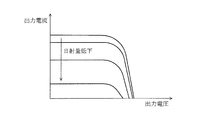
- FIG. 15 is a graph showing an example of characteristics of a general solar cell.
- the horizontal axis indicates the output voltage of the solar cell
- the vertical axis indicates the output current of the solar cell.
- the output characteristics of the solar cell greatly vary depending on the amount of solar radiation, and in particular, the output current width varies greatly.
- connection matching device when the electric power generated by the solar cell is used as commercial power, it is necessary to match the DC output power of the solar cell with the AC frequency and voltage of the commercial power.
- a device that performs this matching is called a connection matching device, but in order to keep the efficiency of matching in the connection matching device high, instead of directly inputting the output of the solar cell to the connection matching device, It is preferable to convert the input voltage and input current into a range in which the efficiency of the interconnection matching device can be kept high before inputting to the interconnection matching device.
- a circuit that performs this conversion is called a power conversion circuit.
- a power converter circuit has high conversion efficiency in a wide input current area according to the output characteristic of a solar cell with a large fluctuation range.
- a power conversion circuit in order to maintain high conversion efficiency for a wide input current range, high conversion efficiency is required even when the output current range is wide.
- the output voltage is maintained at a constant value, it is possible to realize a power conversion circuit having high conversion efficiency in a predetermined range of output current, but power that maintains high conversion efficiency in a wide output current range. It is difficult to realize a conversion circuit.
- the conversion efficiency of the power conversion circuit is lowered. In other words, when a large current is required as the output current, a power conversion circuit having high conversion efficiency may be used when the output current is a large current, but when a small current is output by the power conversion circuit, Conversion efficiency may be reduced.
- the frequency or control method (PWM The control conditions such as PFM) are changed. For example, when the output current is large, PWM control with a constant frequency is performed, and when the output current is small, the circuit is controlled as PFM control with a constant ON width.
- Patent Document 1 discloses a power supply apparatus having a plurality of power conversion circuits having the same configuration and increasing or decreasing the number of circuits to be used according to the output current.
- a power conversion circuit corresponding to the output current can be configured, and high conversion efficiency can be maintained in a wider output current region than when a single power conversion circuit is used.
- the power supply device of Patent Document 1 can widen the range of the output current region in which high conversion efficiency can be maintained by increasing the number of circuits to be combined, but the range is also limited, and the output of the solar cell is efficiently It's not enough to take it out. Since the power supply device of Patent Document 1 combines circuits having the same configuration, the number of required circuits is relatively large, and thus there is a problem that the power supply device is increased in size and cost. Further, in order to construct an optimum power conversion circuit in a wide output current range by combining circuits having the same configuration, there is a problem that the circuit design becomes complicated and the time required for the circuit design becomes long.
- An object of the present invention is to provide a power converter that has a wide input current range and an output current range, efficiently outputs power in response to fluctuations in input current over a wide range, and can be reduced in size and cost. Is to provide.
- a power conversion device is a power conversion device that converts input power input as DC power and outputs output power, the output power detection unit detecting the output power, Based on the detection value of the output power detection unit, a plurality of power conversion circuit units having a portion overlapping the input current range different from and adjacent to the input current range, which is to convert the input power.
- a power conversion control unit that selects one power conversion circuit unit from among the plurality of power conversion circuit units and performs maximum power point tracking control on the selected one power conversion circuit unit;
- the power conversion device of one embodiment has a wide input current range and an output current range, and efficiently outputs power in response to fluctuations in the input current over a wide range, and can be reduced in size and cost. Is possible.
- FIG. 6 is a flowchart illustrating an example of an operation of the power conversion apparatus according to the second embodiment. It is a figure for demonstrating selection of the power inverter circuit unit in the power converter device which concerns on Embodiment 2.
- FIG. It is a graph which shows the example of the characteristic of a solar cell.
- FIG. 1 is a block diagram showing a configuration of a photovoltaic power generation system using a power conversion device according to an embodiment.
- a photovoltaic power generation system that is used in conjunction with a commercial power system can be realized. it can.
- This solar power generation system further transforms the solar cell PV, the power conversion device 100 (or 100B) connected to the solar cell PV, and the output converted by the power conversion device 100, or performs DC-AC conversion, etc.
- the interconnection matching device 200 for matching with the commercial power system is provided, and the interconnection matching device 200 is connected to the commercial power system.
- the solar cell PV generates power according to the amount of solar radiation and outputs power.
- the power conversion device 100 (or 100B) converts the input power with high conversion efficiency and outputs it. Details of the power conversion apparatus 100 (or 100B) will be described later.
- the interconnection matching device 200 includes, for example, a DC-AC inverter circuit, and converts the output from the power conversion device 100 into an AC voltage of about 100V or about 200V of commercial power so that the output can be transmitted to the commercial power system.
- the power output from the solar cell PV generated by the incidence of sunlight is input to the power conversion device 100.
- the power converter 100 the output from the solar cell PV is used as input, and the power is converted with high conversion efficiency regardless of the range of the input current value.
- the power converted by the power conversion device 100 is input to the interconnection matching device 200, is appropriately converted so that it can be transmitted through the commercial power system, and is transmitted to the commercial power system. Thereby, the output from the solar cell PV can be sold effectively.
- the input side of the power converter 100 can be connected to the solar battery PV
- the output side can be connected to the storage battery
- the power generated by the solar battery PV can be stored in the storage battery.
- Embodiment 1 By using the power conversion device 100 according to the first embodiment, it is possible to configure a photovoltaic power generation system that can extract the output from the solar cell PV with high conversion efficiency.
- a power conversion apparatus 100 according to Embodiment 1 will be described with reference to the drawings.
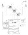
- FIG. 2 is a block diagram showing an example of the configuration of the power conversion apparatus according to this embodiment.
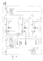
- FIG. 3 is an explanatory diagram in which a part of an example of the configuration of the power conversion device according to the present embodiment is a circuit diagram, and a solar cell PV is connected to the power conversion device 100 according to the first embodiment.
- the power conversion apparatus 100 includes a power conversion control unit 1, an input current detection unit 2 that detects an input current Iin that is a current of the input power Pin, and an input voltage Vin that is a voltage of the input power Pin.
- Input voltage detection unit 3 for detecting power
- first power conversion circuit unit 4 for performing power conversion
- second power conversion circuit unit 5 and third power conversion circuit unit 6 for detecting output power Pout.
- output power detection unit 7 for detecting output power Pout.
- an alarm output unit 9 for outputting an alarm signal.
- the output power Pout is represented by the product of the output current Iout that is the current of the output power Pout and the output voltage Vout that is the voltage of the output power Pout.
- the first to third power conversion circuit units 4 to 6 are circuits each configured to convert and output input power, and these have different input current ranges.
- the first to third power conversion circuit units 4 to 6 receive the power input to the power conversion apparatus 100, and the input is controlled by the power conversion control unit 1.
- the first to third power conversion circuit units 4 to 6 are switching elements FET1, FET2, and FET3, commutation diodes D1, D2, and D3, and inductors for storing energy during power conversion.
- a certain coil (reactor) L1, L2, L3 and capacitors C1, C2, C3 are provided.
- All of the switching elements FET1 to FET3 may be MOSFETs (Metal-Oxide-Semiconductor Field-Effect Transistors: metal-oxide-semiconductor field effect transistors).
- the commutation diodes D1 to D3 may be ordinary diodes or Zener diodes.
- the first to third power conversion circuit units 4 to 6 constitute a step-down DC / DC converter.
- the gates of the switching elements FET1 to FET3 are respectively connected to the power conversion control unit 1 and are controlled to be turned on and off by the drive signals S1 to 3 transmitted from the power conversion control unit 1.
- the power conversion control unit 1 can select which of the first to third power conversion circuit units 4 to 6 is used to convert the output of the solar cell PV, and the power conversion control unit 1 further selects the first Each of the 3 to 3 power conversion circuit units 4 to 6 is controlled.
- the inductances of the coils L1 to L3 have different values, and the values of the output power with respect to the input current are different from each other.
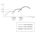
- FIG. 4 is a graph showing the relationship between the input current and the output power of each power conversion circuit unit of the power conversion apparatus according to this embodiment.
- the first to third power conversion circuit units 4 to 6 have different characteristics of the output power Pout with respect to the input current Iin.
- the value of the input current Iin when obtaining the peak output power in each of the first to third power conversion circuit units 4 to 6 is also different from each other in each power conversion circuit unit.
- the input current ranges of the first to third power conversion circuit units 4 to 6 are different from each other and have a portion overlapping with the adjacent input current range. That is, as shown in FIG. 4, the input current ranges of the first power conversion circuit unit 4 and the second power conversion circuit unit 5 are adjacent to each other, and these current ranges are overlapped (in FIG. 4, a broken line). (See the part shown in). Similarly, the input current ranges of the second power conversion circuit unit 5 and the third power conversion circuit unit 6 are adjacent to each other, and these current ranges overlap (see the portion indicated by the broken line in FIG. 4).
- the boundary of the input current Iin of each power conversion circuit unit that can obtain the largest output power Pout is The threshold values Ith1 and Ith2, which are located on the small current side, are designated as the small current side threshold value Ith1, and those located on the large current side are designated as the large current side threshold value Ith2.
- the input current Iin is smaller than the small current side threshold value Ith1, it is preferable to perform power conversion by the first power conversion circuit unit 4, and when the input current Iin is equal to or larger than the small current side threshold value Ith1, the large current side threshold is set.
- the value is smaller than the value Ith2, it is preferable to perform power conversion by the second power conversion circuit unit 5, and when the input current Iin is greater than or equal to the large current side threshold value Ith2, power conversion is performed by the third power conversion circuit unit 6. Preferably it is done.
- the power is set to the second threshold value Pth2.
- the power conversion circuit unit used for power conversion is selected using the first threshold value Pth1 and the second threshold value Pth2. By selecting the power conversion circuit unit using the output power as a result of power conversion, the power conversion circuit unit can be selected more accurately.
- the conversion efficiency of the first to third power conversion circuit units 4 to 6 varies depending on the values of the input current Iin and the output current Iout. In particular, the level of conversion efficiency is determined by the inductance and DC resistance of the coils L1-3.
- FIG. 5 is a graph showing an example of the relationship between the output current and the conversion efficiency in the power conversion circuit unit.
- FIG. 5A is a graph related to a power conversion circuit unit that is preferable when the output current Iout is relatively large
- FIG. 5B is a graph related to a power conversion circuit unit that is preferable when the output current Iout is relatively small.
- the conversion efficiency ⁇ is the ratio of the output power Pout to the input power Pin, and it can be said that the conversion efficiency ⁇ is a power conversion circuit unit capable of performing power conversion with higher efficiency as the conversion efficiency ⁇ increases.
- Each of the power conversion circuit units used in FIGS. 5A and 5B is a power conversion circuit unit having a circuit configuration similar to that of the first to third power conversion circuit units 4 to 6,
- the coils have different inductances.
- 5A operates under the conditions of an input voltage of 120 V, an output voltage of 100 V, and an output current of about 0.2 A to 10 A, and can obtain the highest conversion efficiency ⁇ when the input current is around 10 A.
- a coil capable of outputting a large current is selected for the power conversion circuit unit.
- a large current type coil has a relatively small L value of 0.1 ⁇ H to several ⁇ H, and PWM (Pulse Width Modulation) switching control is performed at a high frequency of 300 KHz to 1 MHz. % Or more can be realized.
- PWM Pulse Width Modulation
- the power conversion circuit unit in FIG. 5B operates under conditions of an input voltage of 120 V, an output voltage of 100 V, and an output current of about 0 A to 1 A so that the highest conversion efficiency ⁇ can be obtained when the input current is around 1 A.
- a coil capable of outputting a small current is selected for the power conversion circuit unit.
- a small current type coil has an L value of several tens of ⁇ H to several hundred ⁇ H, and PWM switching control is performed at a relatively low frequency of 300 KHz or less, so that the conversion efficiency is 90% in a current range of about 0.01 A to 1 A. Front and back can be realized. However, when the output current exceeds 1 A, the output decreases, and it is not suitable for outputting a large current.
- the first to third power conversion circuit units 4 to 6 perform power conversion with high conversion efficiency in different input current ranges, and are scheduled to be input to the power conversion device 100 depending on the input current ranges.
- the input current range can be covered.
- the first to third power conversion circuit units 4 to 6 are not limited to the circuit configuration shown in FIG. 3 as long as the converters have different input current ranges in which high conversion efficiency can be obtained. . What is necessary is just to design according to the intended purpose of the power converter device 100, respectively.
- a bipolar transistor may be used as the switching element instead of the MOSFET.
- a power conversion circuit unit that operates in the same manner as the first to third power conversion circuit units 4 to 6 can be configured by using a switching element such as a MOSFET or a bipolar transistor instead of the commutation diode and using a synchronous rectification type. Can do.
- a power conversion circuit unit having a configuration different from that of the first to third power conversion circuit units 4 to 6 may be used.
- a boost type or a step-up / down type may be used.
- the number of power conversion circuit units is not limited to three as long as it is plural. The circuit configuration and the number of the power conversion circuit units may be appropriately adjusted according to the input current range of the power conversion device 100 determined according to the output of the power source connected to the power conversion device 100 and the like.
- the input current detection unit 2 detects the value of the input current Iin as needed and transmits it to the power conversion control unit 1.
- the input current detection unit 2 is configured using, for example, a current detection resistor, has an A / D converter, converts an analog signal detection value into a digital signal, and transmits the digital signal to the power conversion control unit 1.
- the input voltage detection unit 3 detects the value of the input voltage Vin as needed and transmits it to the power conversion control unit 1.
- the input voltage detection unit 3 is configured using, for example, a voltage dividing resistor, has an A / D converter, converts an analog signal detection value into a digital signal, and transmits the digital signal to the power conversion control unit 1.
- the output power detection unit 7 detects the value of the output power Pout as needed and transmits it to the power conversion control unit 1.
- it is configured using, for example, a current detection resistor and a voltage dividing resistor, and has an A / D converter, which converts the detected value of the analog signal into a digital signal and transmits it to the power conversion control unit 1. Since the output power Pout is a product of the output current Iout and the output voltage Vout, the output power detection unit 7 is configured by the output current detection unit, the output voltage detection unit, and an integrator that integrates these detection values. May be.
- the alarm output unit 9 receives the signal from the power conversion control unit 1 and outputs an alarm signal to notify the operator that an abnormality has occurred in the operation of the power conversion device 100.
- the alarm output unit 9 is a buzzer for notifying the operator of an abnormality by sounding an alarm sound, an alarm lamp (lamp) for notifying the operator of an abnormality by lighting or flashing, and displaying characters or the like on the display screen indicating the abnormality.
- a display device or the like that informs the operator may be used.
- the power conversion control unit 1 includes a threshold storage unit 11, a selection unit 12, a drive control unit 13, and a temporary storage unit 14.
- the power conversion control unit 1 can be configured using, for example, a CPU, a nonvolatile memory, a RAM, and the like.
- the power conversion control unit 1 selects one power conversion circuit unit from the first to third power conversion circuit units 4 to 6 based on the output power Pout detected by the output power detection unit 7. Furthermore, the power conversion control unit 1 controls the power conversion circuit unit so that the selected power conversion circuit unit can obtain the largest output power Pout.
- the threshold storage unit 11 is, for example, a non-volatile memory, and stores the first threshold Pth1 and the second threshold Pth2 described in FIG.
- the first threshold value Pth1 and the second threshold value Pth2 are set as boundaries when the first to third power conversion circuit units 4 to 6 are switched based on the output power Pout.
- the first threshold value Pth1 is a preferable upper limit value of the output power Pout for the first power conversion circuit unit 4
- the second threshold value Pth2 is a preferable upper limit value of the output power Pout for the second power conversion circuit unit 5. It is. Since the third power conversion circuit unit 6 is the power conversion circuit unit on the largest current side, the threshold value indicating the upper limit value of the third power conversion circuit unit 6 may not be set.
- the threshold value may be obtained by actual measurement using the power conversion device 100 having the first to third power conversion circuit units 4 to 6 and stored in the threshold value storage unit 11 in advance.
- the output power Pout is less than or equal to the first threshold value Pth1, it is preferable to perform power conversion by the first power conversion circuit unit 4.
- the output power Pout is greater than the first threshold value Pth1 and less than or equal to the second threshold value Pth2, it is preferable to perform power conversion by the second power conversion circuit unit 5.
- the output power Pout is larger than the second threshold value Pth2, it is preferable to perform power conversion by the third power conversion circuit unit 6.
- the first threshold value Pth1 and the second threshold value Pth2 stored in the threshold value storage unit 11 will be described with reference to FIGS.
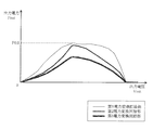
- FIG. 6 is a diagram showing the relationship between the output voltage and the output power of each power conversion circuit unit when the peak value of the output power is equal to the first threshold value Pth1
- FIG. FIG. 8 is a diagram showing the relationship between the output voltage and output power of each power conversion circuit unit when equal to the threshold value Pth2
- FIG. 8 shows the output of each power conversion circuit unit in a state where it is preferable to use the third power conversion circuit unit 6; It is a figure which shows the relationship between a voltage and output electric power. 6 to 8, the vertical axis represents the output power Pout, and the horizontal axis represents the output voltage Vout.
- the peak value of the output power Pout when the first power conversion circuit unit 4 is used is the output power when the second power conversion circuit unit 5 and the third power conversion circuit unit 6 are used.
- the output power Pout is such that a larger output power Pout can be obtained when the second power conversion circuit unit 5 is used.
- the value is set as the first threshold value Pth1.
- the peak value of the output power Pout is largest when the second power conversion circuit unit 5 is used.
- the peak value of the output power Pout when the second power conversion circuit unit 5 is used is the output power when the first power conversion circuit unit 4 and the third power conversion circuit unit 6 are used.
- the output power Pout is such that a larger output power Pout can be obtained when the third power conversion circuit unit 6 is used.
- the value is set as the second threshold value Pth2.
- the peak value of the output power Pout is largest when the third power conversion circuit unit 6 is used.
- the peak value of the output power Pout when the third power conversion circuit unit 6 is used is the output power Pout when the first power conversion circuit unit 4 and the second power conversion circuit unit 5 are used. It is larger than the peak value.
- the output power Pout takes such a value, it is preferable to perform power conversion using the third power conversion circuit unit 6.
- the selection unit 12 selects a power conversion circuit unit based on the output power Pout detected by the output power detection unit 7 and the threshold values Pth1 and Pth2 stored in the threshold value storage unit 11. Specifically, the selection unit 12 compares the detected output power Pout with the first threshold value Pth1, and if the output power Pout is equal to or less than the first threshold value Pth1, the selection unit 12 turns the first power conversion circuit unit 4 on. select. If the detected output power Pout is greater than the first threshold value Pth1 and less than or equal to the second threshold value Pth2, the selection unit 12 selects the second power conversion circuit unit 5. When the detected output power Pout is larger than the second threshold value Pth2, the selection unit 12 selects the third power conversion circuit unit 6.
- the drive control unit 13 controls one of the power conversion circuit units selected by the selection unit 12 so that the largest output power Pout can be obtained.
- the drive control unit 13 controls the drive signals S1 to S3 by transmitting them to the first to third power conversion circuit units 4 to 6, respectively.
- the drive signals S1 to S3 are signals for the first to third power conversion circuit units 4 to 6 to perform PWM switching control, and are signals that repeat ON and OFF at a constant cycle. By this signal, the switching frequency and the ON / OFF duty ratio of the first to third power conversion circuit units 4 to 6 are controlled.
- the drive control unit 13 drives the first to third power conversion circuit units 4 to 6 by maximum power point tracking control (MPPT control).
- MPPT Maximum Power Point Tracking
- control is a control method that can always extract the maximum power from a power source whose output changes, such as a solar cell PV.
- the IV characteristics of the solar cell PV change with changes in solar radiation intensity or module temperature.
- control may be performed so as to follow the maximum power point.
- the output voltage of the solar cell PV is changed (for example, increased), and when the output power of the solar cell tends to increase, the output voltage is continuously changed (increased) in the same manner.
- the output voltage of the solar cell PV is changed (for example, increased), the output voltage is changed (decreased) in the reverse direction when the output power of the solar cell tends to decrease.
- FIG. 9 is a diagram showing IV characteristics and PV characteristics in the output of a solar cell for explaining general MPPT control.
- the IV characteristic at the output of the solar cell PV can be represented by the current-voltage curve of FIG.
- the PV characteristic of the solar cell corresponding to this current-voltage curve can be represented by a power-voltage curve indicated by a broken line.
- Pmax peak value at which the output power is maximum in the power-voltage curve.
- the output power is also decreased.
- the output power increases and approaches Pmax. That is, it proceeds in the direction of arrow A on the PV curve and approaches the peak value (Pmax).
- the output voltage will eventually become larger than the voltage value that takes Pmax.
- the output voltage is Vb (point b).
- the output power decreases.
- the output power increases and approaches Pmax. That is, it proceeds in the direction of arrow B on the PV curve and approaches the peak value (Pmax).
- the peak value of the output power can be followed while the value of the output voltage increases or decreases. Even if the PV characteristics fluctuate due to changes in solar radiation intensity or the like, the peak value (Pmax) of the output power can be followed.
- the MPPT control is performed by adjusting the output voltage Vout according to the change in the output power Pout when the output voltage Vout of the power converter 100 is changed. It can be carried out. In order to increase or decrease the output voltage Vout, the duty ratio of the drive signals S1 to S3 may be increased or decreased. In this way, the MPPT control may be performed so that the output power Pout takes the maximum value.
- the temporary storage unit 14 is composed of a RAM or the like, and temporarily stores the output power Pout detected by the output power detection unit 7.
- MPPT control the output voltage Vout of the power conversion circuit unit is changed, and the output powers Pout before and after the change of the output voltage Vout are compared with each other.
- the temporary storage unit 14 may store a plurality of output powers Pout at different times.
- FIG. 10 is a flowchart illustrating an example of the operation of the power conversion device according to the first embodiment.
- FIG. 11 illustrates an example of the operation for selecting the power conversion circuit unit based on the threshold value in the power conversion device according to the first embodiment.
- FIG. 12 is a flowchart showing an example of MPPT control.
- the power generated by the solar cell PV is input to the power conversion device 100, and is converted and output.
- the power generation amount of the solar cell PV changes due to changes in solar radiation intensity, etc.
- the power conversion device 100 can always perform power conversion with high conversion efficiency.
- the power conversion circuit unit set as a default is driven (# 11). If the first power conversion circuit unit 4 is set as a default, the drive control unit 13 drives the first power conversion circuit unit 4 by PWM switching control. Specifically, the drive signal S2 and the drive signal S3 are OFF, and only the drive signal S1 is sent by the drive control unit 13.
- the first power conversion circuit unit 4 is driven by the MPPT control by the drive control unit 13 (# 12). Thereby, the 1st power inverter circuit unit 4 outputs the largest output electric power Pout.
- the MPPT control operation will be described later with reference to FIG.
- the selection unit 12 determines whether the power conversion circuit unit needs to be switched (# 13). When it is determined that the power conversion circuit unit needs to be switched (Yes in # 13), the power conversion circuit unit is switched (# 14).
- the selection unit 12 selects one power conversion circuit unit that can obtain preferable output power from the first to third power conversion circuit units 4 to 6, and the selected power conversion circuit unit is currently driven. When it is different from the power conversion circuit unit, that is, the first power conversion circuit unit 4, the selection unit 12 determines that the selected power conversion circuit unit needs to be switched.
- the drive control unit 13 sets the drive signal S1 to OFF and the drive signal Only S2 is sent (# 14), and the process returns to step # 12.
- the selection unit 12 determines that switching of the power conversion circuit unit is not necessary (No in # 13). ). In this case, the process returns to step # 12 as it is. That is, the drive control unit 13 sends only the drive signal S1, and the first power conversion circuit unit 4 is continuously driven by the MPPT control (# 12).
- the output current from the input current detection unit 2 is set to a predetermined value in the power conversion control unit 1. What is necessary is just to have a function of detecting the following state and terminating the loop of FIG. 10 by interrupt processing or the like.
- the optimum MPPT of the power conversion circuit unit after switching is determined from the MPPT control condition (for example, the duty ratio of the drive signal) of the power conversion circuit unit before switching. It is preferable to calculate the control condition and start the MPPT control after switching under the calculated MPPT control condition. As a result, it is not necessary to obtain the optimum MPPT control condition from the initial state after switching, and stable MPPT control can be performed immediately after switching.
- the MPPT control condition for example, the duty ratio of the drive signal
- the selection unit 12 selects one power conversion circuit unit based on the output power Pout detected by the output power detection unit 7 every time a predetermined time elapses.
- the predetermined time can be, for example, 10 to 100 ms, 100 to 1000 ms, or 1 to 10 seconds, but is preferably about 1 to 10 seconds.
- the output power Pout is detected by the output power detection unit 7 (# 21).
- the selection unit 12 compares the detected value of the output power Pout with the first threshold value Pth1 stored in the threshold value storage unit 11 (# 22). If the detected value of the output power Pout is equal to or less than the first threshold value Pth1 (Yes in # 22), the selection unit 12 selects the first power conversion circuit unit 4 as one preferable power conversion circuit unit (# 23).
- the detected value of the output power Pout is larger than the first threshold value Pth1 (No in # 22)
- the detected value of the output power Pout and the second threshold value Pth2 stored in the threshold value storage unit 11 Are compared by the selection unit 12 (# 24). If the detected value of the output power Pout is equal to or less than the second threshold value Pth2 (Yes in # 24), the second power conversion circuit unit 5 is selected by the selection unit 12 as a preferred power conversion circuit unit (# 25).
- the third power conversion circuit unit 6 is selected by the selection unit 12 as one preferable power conversion circuit unit (# 26).
- the selection unit 12 If one power conversion circuit unit selected by the selection unit 12 is the same as the currently driven power conversion circuit unit, it is not necessary to switch the power conversion circuit unit (No in # 13 of FIG. 10). When the circuit units are different from each other, the power conversion circuit unit needs to be switched (Yes in # 13 of FIG. 10).
- the output power Pout is detected by the output power detection unit 7, and the detected output power Pout is stored in the temporary storage unit 14 (# 31).
- the drive control unit 13 controls a power conversion circuit unit that is currently performing power conversion.
- the duty ratio of the drive signal is increased by the drive control unit 13 (# 32).
- the output voltage Vout increases.
- the output power Pout when the output voltage Vout increases is detected by the output power detection unit 7, and the detected output power Pout is stored in the temporary storage unit 14 (# 33).
- the output powers Pout stored in the temporary storage unit 14 before (before increase) and after (after increase) the duty ratio are compared with each other by the drive control unit 13 (# 34), and after the change of the duty ratio If the output power Pout is increasing (Yes in # 34), the process returns to # 32 again. Note that the case where the output powers Pout before and after the change of the duty ratio are equal is also included in this case.
- the drive control unit 13 decreases the duty ratio (# 35). As a result, the output voltage Vout decreases.
- the output power Pout when the output voltage Vout decreases is detected by the output power detection unit 7, and the detected output power Pout is stored in the temporary storage unit 14 (# 36).
- the output powers Pout stored in the temporary storage unit 14 before (before decrease) and after (after decrease) the duty ratio are compared with each other by the drive control unit 13 (# 37), and after the change in the duty ratio If the output power Pout is increasing (Yes in # 37), the process returns to # 35 again. Note that the case where the output powers Pout before and after the change of the duty ratio are equal is also included in this case.
- step # 32 If the output power Pout decreases after the duty ratio is changed (No in # 37), the process returns to # 32.
- the above steps may be repeated for a predetermined time as step # 12 in FIG. 10 and then proceed to step # 13 in FIG.
- the MPPT control allows the power conversion device 100 to always extract the maximum output power Pout even if the output of the solar cell PV changes due to changes in solar radiation intensity or module temperature.
- the change direction of the duty ratio is reversed (increase ⁇ decrease or decrease ⁇
- a hysteresis may be provided for the determination of increase or decrease in the output power Pout for a predetermined time thereafter.
- the power conversion control unit 1 may send a signal to the alarm output unit 9 to output an alarm.
- the power conversion control unit 1 may send a signal to the alarm output unit 9.
- the fluctuation range per predetermined time of the input current Iin detected by the input current detection unit 2 and the fluctuation range per predetermined time of the input voltage Vin detected by the input voltage detection unit 3 are represented by the power conversion control unit. It may be calculated by 1. These values are compared with a predetermined set value stored in advance, and if either value is greater than or equal to this set value, a signal is transmitted to the alarm output unit 9, the alarm output unit 9 outputs an alarm signal, The operator may be notified. For example, the lamp may be turned on, an alarm sound may be generated, or a warning display may be displayed on the display screen.
- the PWM switching control is used for the control of the first to third power conversion circuit units 4 to 6.
- any control method such as PFM control may be used as long as power conversion can be performed.
- the power conversion device 100 has power conversion circuit units 4 to 6 having different input current-output power characteristics, and can maintain high conversion efficiency in a wide input current range by switching them. . Therefore, the configuration is not complicated and can be simplified, and the circuit design is easy. In addition, compared to power converters that have multiple identical circuits and combine them to accommodate a wide input current range, the increase in the number of parts for configuring the circuit is suppressed and a wide input current range is achieved. On the other hand, an output can be obtained efficiently. Therefore, downsizing and cost reduction are possible.
- the power conversion device 100 which of the power conversion circuit units 4 to 6 is used is selected based on the output power.
- the power conversion circuit unit that performs power conversion is selected based on the actual detection value, a more preferable power conversion circuit unit is selected, and highly efficient power conversion is possible.
- the power conversion device 100 includes a plurality of power conversion circuit units 4 to 6, and a selection unit 12 selects a preferred power conversion circuit unit from these based on the output power Pout. MPPT control is performed in the selected power conversion circuit unit.
- the power conversion device 100B drives the output power Pout of the power conversion circuit unit that is currently driven after switching the power conversion circuit unit and before switching. Compared with the output power Pout of the power conversion circuit unit, the power conversion is performed in the power conversion circuit unit with the larger output power Pout.
- the power conversion device 100B according to the second embodiment will be described, but the same members as those of the power conversion device 100 according to the first embodiment are denoted by the same reference numerals, and the description of the same points is omitted.
- the power conversion device 100B according to the second embodiment has the same configuration as that of the power conversion device 100 according to the first embodiment, but includes a drive control unit 13 and a temporary storage unit (output).
- the power storage unit 14 has the following functions in addition to the functions described in the first embodiment. Since members other than these are the same as those in the first embodiment, description thereof is omitted.
- the drive control unit 13 After switching the power conversion circuit unit, the drive control unit 13 outputs the output power Pout in the power conversion circuit unit after switching, and the output power Pout in the power conversion circuit unit before switching stored in the temporary storage unit 14. If the output power Pout in the power conversion circuit unit before switching is larger, the power conversion circuit unit before switching is driven again instead of the power conversion circuit unit after switching.
- the temporary storage unit 14 includes an output power storage unit, and is detected by the output power detection unit 10 when the selection unit 12 selects a power conversion circuit unit that is different from the power conversion circuit unit that is currently driven.
- the output power Pout compared with the threshold value is stored.
- FIG. 13 is a flowchart illustrating an example of the operation of the power conversion apparatus according to the second embodiment.
- the power generated by the solar cell PV is input to the power conversion device 100B, converted into power, and output.
- the amount of power generated by the solar cell PV changes due to changes in solar radiation intensity, etc., power conversion with a high conversion efficiency is always possible with the power conversion device 100B.
- the power conversion circuit unit set as a default is driven (# 41). If the first power conversion circuit unit 4 is set as a default, the drive control unit 13 drives the first power conversion circuit unit 4 by PWM switching control. Specifically, the drive signal S2 and the drive signal S3 are OFF, and only the drive signal S1 is sent by the drive control unit 13.
- the first power conversion circuit unit 4 is driven by the MPPT control by the drive control unit 13 (# 42). Thereby, the 1st power inverter circuit unit 4 outputs the largest output electric power Pout. Note that MPPT control has been described above with reference to FIG.
- the selection unit 12 determines whether the power conversion circuit unit needs to be switched (# 43). When it is determined that the power conversion circuit unit needs to be switched (Yes in # 43), the power conversion circuit unit is switched (# 44).
- the selection unit 12 selects one power conversion circuit unit that can obtain preferable output power from the first to third power conversion circuit units 4 to 6, and the selected power conversion circuit unit is currently driven. When it is different from the power conversion circuit unit, that is, the first power conversion circuit unit 4, the selection unit 12 determines that the selected power conversion circuit unit needs to be switched.
- the drive control unit 13 sets the drive signal S1 to OFF and the drive signal Send only S2.
- the selection unit 12 determines that switching of the power conversion circuit unit is not necessary (No in # 43). ). In this case, the process returns to step # 42. That is, the drive control unit 13 sends only the drive signal S1, and the first power conversion circuit unit 4 is continuously driven by the MPPT control (# 42).
- the output power Pout compared with the threshold value when the selection unit 12 selects one power conversion circuit unit is stored in the temporary storage unit 14. Stored (# 44).
- the value stored by the temporary storage unit 14 at this time can be said to be the maximum output power Pout that the first power conversion circuit unit 4 can output with respect to the current output of the solar cell PV.
- the drive control unit 13 turns off the drive signal S1 and sends only the drive signal S2.
- the second power conversion circuit unit 5 is driven by the MPPT control by the drive control unit 13 (# 46).
- the drive control unit 13 determines whether a predetermined time has elapsed (# 47). If the predetermined time has not elapsed (No in # 47), the drive control unit 13 continues the MPPT control.
- the predetermined time may be a sufficient time for the second power conversion circuit unit 5 to output the largest output power Pout by MPPT control.
- the output power detection unit 10 detects the output power Pout. .
- the detected value is compared with the output power Pout stored in the temporary storage unit 14 in the step # 44 by the drive control unit 13 (# 48).
- the power conversion control unit 1 is connected to the input current detection unit 2. It is sufficient to provide a function of detecting a state in which the output current is less than or equal to a predetermined value and terminating the loop of FIG. 13 by interrupt processing or the like.
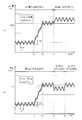
- FIG. 14 is a diagram for explaining selection of a power conversion circuit unit in the power conversion device according to the second embodiment.
- FIG. 14A shows a case where the power conversion circuit unit is not switched after the power conversion circuit unit is switched based on the threshold value of the output power
- FIG. 14B shows the threshold of the output power. This is a case where the power conversion circuit unit is switched again after the power conversion circuit unit is switched based on the value.
- the vertical axis represents solar radiation and output power
- the horizontal axis represents time.
- a solid line indicates the relationship between the output power Pout of the power conversion apparatus 100B and time
- a broken line indicates the relationship between the amount of solar radiation and time. As indicated by a broken line, the amount of solar radiation that was constant until time T1 starts to increase at time T1 and becomes constant at time T2.
- the output power Pout changes at a substantially constant value until time T1.
- the vertical movement width Ph in the minute range (the amount of increase / decrease in the output power Pout in the minute period t1) is set to be larger than the actual value. It shows greatly.
- the minute period t1 is, for example, about 1 msec.
- first, power conversion is performed using the first power conversion circuit unit 4.
- the amount of solar radiation increases, and the output power Pout exceeds the first threshold value Pth1 immediately before time T2, so that the power conversion circuit unit is switched to the second power conversion circuit unit 5.
- Switching to the second power conversion circuit unit 5 is completed at time T3.
- the output power Pout is increased by switching to the second power conversion circuit unit 5 as compared to before switching. Therefore, power conversion is performed using the second power conversion circuit 5 as it is.
- the selected output power of the power conversion circuit unit is the largest based on the actual output power Pout. It is confirmed whether or not Pout can be output, and power conversion is performed by the power conversion circuit unit that outputs the largest output power Pout. Thereby, the power converter device 100B which can perform highly efficient power conversion is realizable.
- the power conversion circuit unit is selected based on the detected output power Pout based on a threshold value obtained by measurement in advance, depending on the value of the output power Pout (for example, a value near the threshold value). There is a possibility that a part other than the power conversion circuit unit capable of obtaining the largest output power Pout may be selected. As this reason, there is a possibility that the stored threshold value is shifted. The reason why the threshold value is deviated may be an error peculiar to each power converter, an influence from the usage environment, a change with time of the power converter or the like.
- the power conversion device 100B according to the second embodiment has been described, the power conversion device 100B has the same effects as the power conversion device 100 according to the first embodiment.
- the output power is the largest due to the output power detected by actually driving the selected power conversion circuit unit. Since the power conversion circuit unit is selected, a preferable power conversion circuit unit can be selected more accurately, and highly efficient power conversion can be performed.
- the power conversion devices 100 and 100B according to the present embodiment have power conversion circuit units having different input current-output power characteristics, and by switching them, high conversion efficiency can be maintained in a wide input current range, and high efficiency. Power conversion is possible.
- the power converters 100 and 100B according to the present embodiment are not complicated in configuration and can be simplified, and circuit design is also easy.
- the increase in the number of parts for configuring the circuit is suppressed and a wide input current range is achieved.
- an output can be obtained efficiently. Therefore, downsizing and cost reduction are possible.
- the structure, shape, dimensions, number, material, composition, etc. of the entire power conversion device 100, 100B or each part can be appropriately changed in accordance with the spirit of the present invention.
- the power converters 100 and 100B have a wide input current range and an output current range, and can output maximum power in the entire current range in response to fluctuations in a wide range of input current. And loss is small. Further, downsizing and cost reduction are possible. For example, the power generated by the solar cell can be taken out more effectively by connecting to the solar cell. Therefore, it can be suitably used as a component of a solar power generation system.
Landscapes
- Engineering & Computer Science (AREA)
- Power Engineering (AREA)
- Control Of Electrical Variables (AREA)
- Dc-Dc Converters (AREA)
Abstract
直流電力として入力される入力電力を電力変換して出力電力を出力する電力変換装置であって、出力電力を検出する出力電力検出部と、入力電力を電力変換するものであり、入力電流範囲が互いに異なりかつ隣合う入力電流範囲とは重複する部分を有する複数の電力変換回路部と、出力電力検出部の検出値に基づいて、複数の電力変換回路部のうちから1つの電力変換回路部を選択し、選択した1つの電力変換回路部に対して最大電力点追従制御を行う電力変換制御部と、を有する。
Description
本発明は、直流電力として入力される入力電力を電力変換して出力する電力変換装置、および該電力変換装置を備える太陽光発電システムに関する。
近年、化石燃料の枯渇に対応するため、環境への配慮の必要性等から、再生可能な自然エネルギーの普及が望まれている。特に太陽電池は、環境への影響が少なく、今後の一層の発展が期待される。太陽電池により発電された電力は、蓄電池に蓄電されたり、電力会社に売電されることにより有効に利用されている。太陽電池は日射量により出力が変動することから、天候等により出力が左右されるため、電力の供給量を制御することは困難である。太陽電池の出力の変動幅の全域において、高い変換効率で出力が取り出されることが好ましい。
図15は、一般的な太陽電池の特性の例を示すグラフである。図15において、横軸は、太陽電池の出力電圧を示し、縦軸は太陽電池の出力電流を示す。図15に示されているように、太陽電池の出力特性は、日射量により大きく変動し、特に出力電流幅が大きく変動する。
例えば、太陽電池により発電された電力を商用電力として利用する場合には、太陽電池の直流の出力電力を商用電力の交流周波数と電圧とに整合させる必要がある。この整合を行う装置を連系用整合装置と呼ぶが、連系用整合装置での整合の効率を高く保つために、太陽電池の出力を連系用整合装置に直接に入力するのではなく、連系用整合装置の効率を高く保てる範囲の入力電圧および入力電流に変換してから連系用整合装置に入力することが好ましい。この変換を行う回路を電力変換回路と呼ぶ。そして、電力変換回路は、変動幅の大きい太陽電池の出力特性に合わせて、広い入力電流域において高い変換効率を有することが好ましい。
電力変換回路において、広い入力電流域に対して高い変換効率を維持するためには、出力電流域が広い場合であっても高い変換効率が要求される。出力電圧を一定の値に維持する場合には、所定の範囲の出力電流において高い変換効率を有する電力変換回路を実現することは可能であるが、広い出力電流域において高い変換効率を維持する電力変換回路を実現することは困難である。従来の電力変換回路においては、出力電流が所定の範囲から外れると、電力変換回路の変換効率が低下することになる。つまり、出力電流として大電流が必要な場合には、出力電流が大電流である場合に高い変換効率を有する電力変換回路を用いればよいが、その電力変換回路により小電流を出力させる場合には、変換効率が低下する可能性がある。
単一の電力変換回路により、大電流の出力電流および小電流の出力電流のいずれにおいても高い変換効率を実現するために、出力電流の範囲に応じて、電力変換における周波数または制御方式(PWM・PFM)等の制御条件を変更することが行われている。例えば、出力電流が大きい場合は周波数一定のPWM制御とし、出力電流が小さい場合にはON幅一定のPFM制御として回路を制御することにより対応している。
また、特許文献1には、同じ構成の電力変換回路を複数持ち、出力電流に応じて、使用する回路数を増減する電源装置が開示されている。この電源装置は、複数の回路を組み合わせることで、出力電流に応じた電力変換回路を構成し、単一の電力変換回路を用いる場合よりも広い出力電流域において高い変換効率を維持することができる。
上述したように、単一の電力変換回路において、周波数や制御方式(PWM・PFM)等を変更することで、ある程度の範囲の出力電流域において高い変換効率を維持することは可能である。しかし、その出力電流域の範囲には限界があり、太陽電池の出力を効率よく取り出すには十分な範囲とは言えない。
特許文献1の電源装置は、組み合わせる回路の数を増やすことにより、高い変換効率を維持できる出力電流域の範囲を広げることができるが、その範囲にも限界があり、太陽電池の出力を効率よく取り出すには十分な範囲とは言えない。特許文献1の電源装置は、同じ構成の回路を組み合わせることから、必要とする回路の数が比較的多くなるため、電源装置が大型化、高コスト化するという問題がある。また、同じ構成の回路を組み合わせることにより広い出力電流域において最適の電力変換回路を構成するには、回路の設計が複雑になり、回路設計にかかる時間が長くなるという問題がある。
本発明の目的は、広い入力電流域および出力電流域を持ち、広い範囲での入力電流の変動に対応して効率よく電力を出力し、かつ、小型化・低コスト化が可能な電力変換装置を提供することである。
本発明に係る一実施形態の電力変換装置は、直流電力として入力される入力電力を電力変換して出力電力を出力する電力変換装置であって、前記出力電力を検出する出力電力検出部と、前記入力電力を電力変換するものであり、入力電流範囲が互いに異なりかつ隣合う入力電流範囲とは重複する部分を有する複数の電力変換回路部と、前記出力電力検出部の検出値に基づいて、前記複数の電力変換回路部のうちから1つの電力変換回路部を選択し、選択した前記1つの電力変換回路部に対して最大電力点追従制御を行う電力変換制御部と、を有する。
一実施形態の電力変換装置によれば、広い入力電流域および出力電流域を持ち、広い範囲での入力電流の変動に対応して効率よく電力を出力し、かつ、小型化・低コスト化が可能である。
図1は、実施形態に係る電力変換装置を用いた太陽光発電システムの構成を示すブロック図である。図1に示すように、実施形態1または2に係る電力変換装置100(または100B)および太陽電池PVを用いて、商用電力系統と連系して使用される太陽光発電システムを実現することができる。この太陽光発電システムは、太陽電池PVと、太陽電池PVに接続された電力変換装置100(または100B)と、電力変換装置100により電力変換された出力をさらに変圧したり、直流-交流変換等することで商用電力系統に整合させるための連系用整合装置200とを備え、連系用整合装置200は商用電力系統に接続されている。
太陽電池PVは日射量に応じて発電を行い、電力を出力する。
電力変換装置100(または100B)は、入力された電力を高い変換効率で変換して出力する。電力変換装置100(または100B)の詳細については、後述する。
連系用整合装置200は、例えばDC-ACインバータ回路を備え、電力変換装置100からの出力を商用電力系統に送電できるように、100V程度または200V程度の商用電力の交流電圧へと変換する。
太陽光が入射することで発電した太陽電池PVから出力された電力が、電力変換装置100に入力される。電力変換装置100では、太陽電池PVからの出力を入力とし、その入力電流値の範囲にかかわらず高い変換効率で電力変換して出力する。電力変換装置100により変換された電力は連系用整合装置200に入力され、商用電力系統で伝送可能なように適宜変換され、商用電力系統へと送電される。これにより、太陽電池PVからの出力を有効に売電することができる。
また、電力変換装置100の入力側は太陽電池PVに接続した状態で、出力側を蓄電池に接続して、太陽電池PVにより発電された電力を蓄電池に蓄電することもできる。
(実施形態1)
実施形態1に係る電力変換装置100を用いることにより、太陽電池PVからの出力を高い変換効率で取り出すことができる太陽光発電システムを構成することができる。実施形態1に係る電力変換装置100について、図面を参照して説明する。
実施形態1に係る電力変換装置100を用いることにより、太陽電池PVからの出力を高い変換効率で取り出すことができる太陽光発電システムを構成することができる。実施形態1に係る電力変換装置100について、図面を参照して説明する。
図2は本実施形態に係る電力変換装置の構成の一例を示すブロック図である。図3は本実施形態に係る電力変換装置の構成の一例の一部を回路図とした説明図であって、実施形態1に係る電力変換装置100に太陽電池PVが接続されている。
図2に示すように、電力変換装置100は、電力変換制御部1と、入力電力Pinの電流である入力電流Iinを検出する入力電流検出部2と、入力電力Pinの電圧である入力電圧Vinを検出する入力電圧検出部3と、電力変換を行う第1電力変換回路部4、第2電力変換回路部5および第3電力変換回路部6と、出力電力Poutを検出する出力電力検出部7と、警報信号を出力する警報出力部9とを備えている。なお、出力電力Poutは、出力電力Poutの電流である出力電流Ioutと、出力電力Poutの電圧である出力電圧Voutとの積で表される。
第1~3電力変換回路部4~6は、それぞれ入力電力を変換して出力するように構成された回路であって、これらは互いに入力電流範囲が異なる。第1~3電力変換回路部4~6には、電力変換装置100に入力された電力が入力されるが、その入力は電力変換制御部1により制御されている。
図3に示すように、第1~3電力変換回路部4~6は、スイッチング素子FET1、FET2、FET3と、転流ダイオードD1、D2、D3と、電力変換時にエネルギーを蓄積するためのインダクタであるコイル(リアクトル)L1、L2、L3と、コンデンサC1、C2、C3とを備えている。
スイッチング素子FET1~3は、いずれもMOSFET(Metal-Oxide-Semiconductor Field-Effect Transistor :金属-酸化物-半導体電界効果型トランジスタ)とすればよい。転流ダイオードD1~3は、通常のダイオードであってもツェナーダイオードであってもよい。第1~3電力変換回路部4~6は、降圧型のDC/DCコンバーターを構成している。スイッチング素子FET1~3のゲートは、それぞれ電力変換制御部1に接続されていて、電力変換制御部1から送信される駆動信号S1~3により、ON、OFFが制御される。電力変換制御部1により、太陽電池PVの出力を変換するために第1~3電力変換回路部4~6のいずれを用いるかを選択することができ、さらに電力変換制御部1により、第1~3電力変換回路部4~6のそれぞれが制御される。
第1~3電力変換回路部4~6において、各コイルL1~3のインダクタンスは互いに異なる値を有しており、それぞれにおける入力電流に対する出力電力の値が互いに異なる。
図4を用いて、第1~3電力変換回路部4~6の入力電流Iinと出力電力Poutとの関係について説明する。図4は本実施形態に係る電力変換装置の各電力変換回路部の入力電流と出力電力との関係を示すグラフである。図4に示すように、第1~3電力変換回路部4~6は、それぞれ入力電流Iinに対する出力電力Poutの特性が異なる。各第1~3電力変換回路部4~6におけるピークの出力電力を得るときの入力電流Iinの値も各電力変換回路部において互いに異なる。
第1~3電力変換回路部4~6の各入力電流範囲が互いに異なり、かつ隣合う入力電流範囲とは重複する部分を有している。つまり、図4に示しているように、第1電力変換回路部4および第2電力変換回路部5の入力電流範囲は隣合っていて、これらの電流範囲は重複している(図4において破線で示した部分を参照)。同様に、第2電力変換回路部5および第3電力変換回路部6の入力電流範囲は隣合っていて、これらの電流範囲は重複している(図4において破線で示した部分を参照)。
第1~3電力変換回路部4~6のいずれか1つを用いて電力変換を行う場合に、最も大きな出力電力Poutを得ることができる各電力変換回路部の入力電流Iinの境界が、しきい値Ith1およびIth2であり、小電流側に位置するものを小電流側しきい値Ith1とし、大電流側に位置するものを大電流側しきい値Ith2とする。
入力電流Iinが小電流側しきい値Ith1よりも小さい場合は第1電力変換回路部4により電力変換を行うことが好ましく、入力電流Iinが小電流側しきい値Ith1以上で大電流側しきい値Ith2よりも小さい場合は第2電力変換回路部5により電力変換を行うことが好ましく、入力電流Iinが大電流側しきい値Ith2以上である場合は第3電力変換回路部6により電力変換を行うことが好ましい。
ここで、図4に示すように、入力電流Iin=小電流側しきい値Ith1の場合の出力電力を第1しきい値Pth1とし、入力電流Iin=大電流側しきい値Ith2の場合の出力電力を第2しきい値Pth2とする。本実施形態では、電力変換に用いる電力変換回路部を、第1しきい値Pth1および第2しきい値Pth2を用いて選択する。電力変換された結果としての出力電力を用いて電力変換回路部を選択することで、より正確に電力変換回路部を選択することができる。
第1~3電力変換回路部4~6は、入力電流Iinおよび出力電流Ioutの値により変換効率が変化する。特に、コイルL1~3のインダクタンスおよび直流抵抗により変換効率の高低が決まってくる。図5は、電力変換回路部における出力電流と変換効率との関係の例を示すグラフである。図5(A)は出力電流Ioutが比較的大きい場合に好ましい電力変換回路部に関するグラフであり、図5(B)は出力電流Ioutが比較的小さい場合に好ましい電力変換回路部に関するグラフである。変換効率ηは入力電力Pinに対する出力電力Poutの比であり、変換効率ηが大きいほど高い効率の電力変換が可能な電力変換回路部であるといえる。
図5(A)および図5(B)において用いた電力変換回路部は、いずれも、第1~3電力変換回路部4~6と同様の回路構成を有する電力変換回路部であるが、それぞれのコイルのインダクタンスは互いに異なる。
図5(A)の電力変換回路部は、入力電圧120V、出力電圧100V、出力電流が0.2A~10A程度の条件において動作し、入力電流が10A付近において最も高い変換効率ηを得ることができるように設計されている。この電力変換回路部には、大電流出力が可能なコイルが選択される。一般的に大電流型のコイルはL値が0.1μH~数μHと比較的小さく、300KHz~1MHzの高周波でPWM(Pulse Width Modulation)スイッチング制御することにより、出力電流が10A付近で変換効率90%以上を実現できる。しかし、出力電流が1A以下では自己回路損失が大きいため50%程度まで変換効率ηが低下する。
図5(B)の電力変換回路部は、入力電圧120V、出力電圧100V、出力電流0A~1A程度の条件において動作し、入力電流が1A付近において最も高い変換効率ηを得ることができるように設計されている。この電力変換回路部には、小電流出力が可能なコイルが選択される。一般的に小電流型のコイルはL値が数十μH~数百μHで、300KHz以下の比較的低い周波数でPWMスイッチング制御することにより、0.01A~1A程度の電流域において変換効率90%前後を実現できる。しかし、出力電流が1Aを超えると出力が低下し、大電流を出力するには適していない。
第1~3電力変換回路部4~6は、それぞれ異なる入力電流の範囲において高い変換効率の電力変換がなされ、それらの入力電流の範囲により、電力変換装置100に入力されることが予定されている入力電流の範囲をカバーできる。
なお、第1~3電力変換回路部4~6は、それぞれ高い変換効率を得ることができる入力電流の範囲が異なるコンバーターであればよく、図3に示した回路構成に限定されるわけではない。電力変換装置100の使用目的に応じてそれぞれ設計されればよい。例えば、スイッチング素子としてMOSFETの代わりにバイポーラトランジスタを用いてもよい。また、転流ダイオードの代わりに、MOSFETまたはバイポーラトランジスタといったスイッチング素子を用いて同期整流式としても、第1~3電力変換回路部4~6と同様の動作をする電力変換回路部を構成することができる。また、第1~3電力変換回路部4~6とは異なる構成の電力変換回路部を用いてもよく、例えば昇圧型や昇降圧型でもよい。また、電力変換回路部の数は複数であればよく、3個に限定されるわけではない。電力変換回路部の回路構成およびその数は、電力変換装置100に接続される電力源の出力等に応じて決定される電力変換装置100の入力電流の範囲等に応じて適宜調整すればよい。
入力電流検出部2は、入力電流Iinの値を随時検出し、電力変換制御部1に送信する。入力電流検出部2は例えば電流検出用の抵抗等を用いて構成され、A/D変換器を有し、アナログ信号の検出値をデジタル信号へと変換して電力変換制御部1に送信する。
入力電圧検出部3は、入力電圧Vinの値を随時検出し、電力変換制御部1に送信する。入力電圧検出部3は例えば分圧抵抗等を用いて構成され、A/D変換器を有し、アナログ信号の検出値をデジタル信号へと変換して電力変換制御部1に送信する。
出力電力検出部7は、出力電力Poutの値を随時検出し、電力変換制御部1に送信する。例えば、例えば電流検出用の抵抗および分圧抵抗等を用いて構成され、A/D変換器を有し、アナログ信号の検出値をデジタル信号へと変換して電力変換制御部1に送信する。なお、出力電力Poutは、出力電流Ioutと出力電圧Voutとの積であることから、出力電流検出部、出力電圧検出部およびこれらの検出値を積算する積算器により出力電力検出部7を構成してもよい。
警報出力部9は、電力変換制御部1からの信号を受けて電力変換装置100の動作に異常が生じていることを操作者に知らせるために警報信号を出力する。警報出力部9としては、警報音を鳴らすことで異常を操作者に知らせるブザー、点灯または点滅により異常を操作者に知らせる警報灯(ランプ)、異常であることを表示画面に文字等を表示することにより操作者に知らせる表示装置等とすればよい。
電力変換制御部1は、しきい値格納部11と、選択部12と、駆動制御部13と、一時記憶部14とを備えている。電力変換制御部1は、例えばCPU、不揮発性メモリ、RAM等を用いて構成することが可能である。電力変換制御部1は、出力電力検出部7により検出された出力電力Poutに基づいて、第1~3電力変換回路部4~6のうちから1つの電力変換回路部を選択する。さらに電力変換制御部1は、選択された電力変換回路部が最も大きい出力電力Poutを得ることができるように電力変換回路部を制御する。
しきい値格納部11は、例えば不揮発性メモリであって、図4で述べた第1しきい値Pth1および第2しきい値Pth2を格納している。第1しきい値Pth1および第2しきい値Pth2は、第1~第3電力変換回路部4~6を出力電力Poutに基づいて切換える際の境界として設定されている。ここで、第1しきい値Pth1が第1電力変換回路部4に対する好ましい出力電力Poutの上限値であり、第2しきい値Pth2が第2電力変換回路部5に対する好ましい出力電力Poutの上限値である。第3電力変換回路部6は最も大電流側の電力変換回路部であることから、第3電力変換回路部6の上限値を示すしきい値は設定しなくてもよい。
しきい値は、第1~3電力変換回路部4~6を有する電力変換装置100を用いて実測することで求め、予めしきい値格納部11に格納しておけばよい。出力電力Poutが第1しきい値Pth1以下である場合は第1電力変換回路部4により電力変換を行うことが好ましい。出力電力Poutが第1しきい値Pth1よりも大きく第2しきい値Pth2以下である場合は第2電力変換回路部5により電力変換を行うことが好ましい。出力電力Poutが第2しきい値Pth2よりも大きい場合は第3電力変換回路部6により電力変換を行うことが好ましい。
なお、電力変換回路部の数を増加させる場合には、それに応じてしきい値の数を増加させればよい。
ここで、しきい値格納部11に格納されている、第1しきい値Pth1および第2しきい値Pth2について図6~図8を参照しながら説明する。
図6は出力電力のピーク値が第1しきい値Pth1と等しい場合の各電力変換回路部の出力電圧および出力電力の関係を示す図であり、図7は出力電力のピーク値が第2しきい値Pth2と等しい場合の各電力変換回路部の出力電圧および出力電力の関係を示す図であり、図8は第3電力変換回路部6を用いることが好ましい状態における各電力変換回路部の出力電圧および出力電力の関係を示す図である。図6~図8において縦軸は出力電力Poutであり、横軸は出力電圧Voutである。
図6に示すように、第1電力変換回路部4を用いた場合の出力電力Poutのピーク値が、第2電力変換回路部5および第3電力変換回路部6をそれぞれ用いた場合の出力電力Poutのピーク値よりも大きく、出力電力Poutの値がこの値よりも大きくなると、第2電力変換回路部5を用いた場合の方が大きな出力電力Poutを得ることができるような出力電力Poutの値が、第1しきい値Pth1として設定される。
第1しきい値Pth1よりも出力電力Poutが大きくなったとしたときに、出力電力Poutのピーク値が最も大きくなるのは第2電力変換回路部5を用いた場合となる。
図7に示すように、第2電力変換回路部5を用いた場合の出力電力Poutのピーク値が、第1電力変換回路部4および第3電力変換回路部6をそれぞれ用いた場合の出力電力Poutのピーク値よりも大きく、出力電力Poutの値がこの値よりも大きくなると、第3電力変換回路部6を用いた場合の方が大きな出力電力Poutを得ることができるような出力電力Poutの値が、第2しきい値Pth2として設定される。
第2しきい値Pth2よりも出力電力Poutが大きくなったとしたときに、出力電力Poutのピーク値が最も大きくなるのは第3電力変換回路部6を用いた場合となる。
図8に示すように、第3電力変換回路部6を用いた場合の出力電力Poutのピーク値が、第1電力変換回路部4および第2電力変換回路部5を用いた場合の出力電力Poutのピーク値よりも大きい。出力電力Poutがこのような値をとる場合には、第3電力変換回路部6を用いて電力変換を行うことが好ましい。
選択部12は、出力電力検出部7により検出された出力電力Poutとしきい値格納部11に格納されたしきい値Pth1およびPth2に基づいて電力変換回路部を選択する。具体的には、選択部12は、検出された出力電力Poutと第1しきい値Pth1とを比べ、出力電力Poutが第1しきい値Pth1以下であれば、第1電力変換回路部4を選択する。また、検出された出力電力Poutが第1しきい値Pth1よりも大きく第2しきい値Pth2以下であれば、選択部12は第2電力変換回路部5を選択する。また、検出された出力電力Poutが第2しきい値Pth2よりも大きい場合は、選択部12は第3電力変換回路部6を選択する。
駆動制御部13は、選択部12により選択されたいずれかの電力変換回路部を駆動させ、最も大きな出力電力Poutを得ることができるように制御する。駆動制御部13は、駆動信号S1~S3をそれぞれ第1~3電力変換回路部4~6に送信することによりこれらを制御する。駆動信号S1~S3は、第1~3電力変換回路部4~6がPWMスイッチング制御を行うための信号であり、ONとOFFとを一定の周期で繰り返す信号である。この信号により、第1~3電力変換回路部4~6のスイッチング周波数およびON-OFFのデューティー比が制御される。
さらに、駆動制御部13は、最大電力点追従制御(MPPT制御)により、第1~3電力変換回路部4~6を駆動させている。MPPT(Maximum Power Point Tracking)制御とは、太陽電池PV等のように出力が変化する電源から常に最大電力を取り出すことができる制御方法である。
太陽電池PVのI-V特性は、日射強度またはモジュール温度の変化により変化する。太陽電池PVから常に最大の電力(電圧と電流との積)を取り出すためには、最大電力点を追従するように制御すればよい。具体的には、太陽電池PVの出力電圧を変化(例えば増大)させ、太陽電池の出力電力が増大傾向にあるときには引き続き出力電圧を同じように変化(増大)させる。太陽電池PVの出力電圧を変化(例えば増大)させたときに、太陽電池の出力電力が減少傾向にあるときには出力電圧を逆方向に変化(減少)させる。この制御方法により、太陽電池PVの最大出力点を追従することができる。
MPPT制御について、図を用いて説明する。図9は、一般的なMPPT制御について説明するための太陽電池の出力におけるI-V特性およびP-V特性を示す図である。太陽電池PVの出力におけるI-V特性は、図9の電流-電圧曲線で表すことができる。また、この電流-電圧曲線に対応する、太陽電池のP-V特性は破線で示される電力-電圧曲線で表すことができる。電力-電圧曲線において出力電力が最大となるピーク値(Pmax)が存在する。
出力電圧が、例えばVa(点a)であった場合に出力電圧を減少させると、出力電力も減少する。これに対して出力電圧を増大させると、出力電力が増大し、Pmaxへと近づく。すなわち、P-V曲線において矢印A方向に進んで、ピーク値(Pmax)に近づいていく。
出力電圧が増大していくと、いずれは出力電圧がPmaxをとる電圧値よりも大きくなる。例えば、出力電圧がVb(点b)となる。このとき、出力電圧が増大すれば出力電力が減少する。この場合は、出力電圧を減少させることにより、出力電力が増大し、Pmaxへと近づく。すなわち、P-V曲線において矢印B方向に進んで、ピーク値(Pmax)に近づいていく。この動作を繰り返すことで、出力電圧の値が増減しながら、出力電力のピーク値を追従することができる。日射強度等が変化することによりP-V特性が変動しても、出力電力のピーク値(Pmax)を追従することができる。
この一般的なMPPT制御と同様に本実施形態においては、電力変換装置100の出力電圧Voutを変化させた際の出力電力Poutの変化に応じて、出力電圧Voutを調整することにより、MPPT制御を行うことができる。出力電圧Voutを増減させるためには、駆動信号S1~3のデューティー比を増減させればよい。このようにして、出力電力Poutが最大値をとるようにMPPT制御を行えばよい。
一時記憶部14は、RAM等により構成されていて、出力電力検出部7により検出された出力電力Pout等を一時的に記憶する。MPPT制御においては、電力変換回路部の出力電圧Voutを変化させて、出力電圧Voutの変化前後における出力電力Poutを互いに比較する。このようなときに、一時記憶部14が異なる時間における複数の出力電力Poutを記憶しておけばよい。
次に、図10~図12を用いて実施形態1に係る電力変換装置100の動作について説明する。図10は実施形態1に係る電力変換装置の動作の一例を示すフローチャートであり、図11は実施形態1に係る電力変換装置におけるしきい値に基づく電力変換回路部の選択についての動作の一例を示すフローチャートであり、図12はMPPT制御の一例を示すフローチャートである。
図1に示す太陽光発電システムにおいて、太陽電池PVで発電された電力が電力変換装置100に入力され、電力変換されて出力される。日射強度の変化等により太陽電池PVの発電量は変化するが、電力変換装置100により常時高い変換効率での電力変換が可能である。
図10に示すように、電力変換装置100を使用し始めた際には、デフォルトとして設定されている電力変換回路部が駆動される(#11)。デフォルトとして第1電力変換回路部4が設定されているとすると、駆動制御部13により第1電力変換回路部4がPWMスイッチング制御により駆動される。具体的には、駆動信号S2および駆動信号S3がOFFであり、駆動制御部13により駆動信号S1のみが送られる。
駆動制御部13により、第1電力変換回路部4がMPPT制御により駆動される(#12)。これにより、第1電力変換回路部4は最も大きい出力電力Poutを出力する。なお、MPPT制御の動作については図12で後述する。
第1電力変換回路部4が駆動されている際に、電力変換回路部の切換えが必要であるかについて選択部12により判断される(#13)。電力変換回路部の切換えが必要であると判断された場合には(#13でYes)、電力変換回路部が切り換えられる(#14)。
つまり、選択部12により、第1~3電力変換回路部4~6のうちから好ましい出力電力が得られる1つの電力変換回路部が選択され、選択された電力変換回路部が現在駆動している電力変換回路部、すなわち第1電力変換回路部4とは異なる場合には選択された電力変換回路部に切換えが必要であると選択部12により判断される。
選択部12により、例えば第1電力変換回路部4を第2電力変換回路部5に切換えることが必要であると判断された場合には、駆動制御部13が駆動信号S1をOFFにして駆動信号S2のみを送り(#14)、#12の工程に戻る。
これに対して、選択された電力変換回路部が第1電力変換回路部4である場合には、電力変換回路部の切換えが必要ではないと、選択部12により判断される(#13でNo)。この場合には、そのまま#12の工程に戻る。つまり、駆動制御部13が駆動信号S1のみを送り、第1電力変換回路部4はMPPT制御による駆動が継続される(#12)。
例えば日没等により太陽電池PVでの発電ができなくなった等で電力変換回路部の動作を終了する場合には、例えば電力変換制御部1に、入力電流検出部2からの出力電流が所定値以下となった状態を検出し、割り込み処理等により図10のループを終了する機能を持たせればよい。
なお、#14の工程で電力変換回路部が切り換えられた場合に、切り換え前の電力変換回路部のMPPT制御条件(例えば駆動信号のデューティー比)から、切り換え後の電力変換回路部の最適なMPPT制御条件を算出し、算出されたMPPT制御条件で切り換え後のMPPT制御を開始するとよい。これによって、切り換え後に初期状態から最適なMPPT制御条件を求める必要がなくなり、切り換え直後から安定したMPPT制御が行える。
ここで、図11を用いて、選択部12による1つの電力変換回路部の選択の動作について説明する。選択部12は、所定時間が経過する度に、出力電力検出部7によって検出された出力電力Poutに基づいて1つの電力変換回路部を選択する。この所定時間は、例えば10~100ms、100~1000msまたは1~10秒等とすることが可能であるが、1~10秒程度とすることが好ましい。
出力電力検出部7により、出力電力Poutが検出される(#21)。選択部12により、出力電力Poutの検出値としきい値格納部11に格納された第1しきい値Pth1とが比較される(#22)。出力電力Poutの検出値が第1しきい値Pth1以下であれば(#22でYes)、選択部12により、第1電力変換回路部4が好ましい1つの電力変換回路部として選択される(#23)。
出力電力Poutの検出値が第1しきい値Pth1よりも大きい場合は(#22でNo)、出力電力Poutの検出値と、しきい値格納部11に格納された第2しきい値Pth2とが選択部12により比較される(#24)。出力電力Poutの検出値が第2しきい値Pth2以下であれば(#24でYes)、第2電力変換回路部5が好ましい1つの電力変換回路部として選択部12により選択される(#25)。
出力電力Poutの検出値が第2しきい値Pth2よりも大きい場合は(#24でNo)、第3電力変換回路部6が好ましい1つの電力変換回路部として選択部12により選択される(#26)。
選択部12が選択した1つの電力変換回路部が、現在駆動されている電力変換回路部と同一であれば電力変換回路部を切換える必要がないが(図10の#13でNo)、電力変換回路部が互いに異なる場合には電力変換回路部の切換えが必要である(図10の#13でYes)。
次に、図12を用いてMPPT制御について説明する。まず、出力電力検出部7により出力電力Poutが検出され、検出された出力電力Poutが一時記憶部14により記憶される(#31)。
駆動制御部13により、現在電力変換を行っている電力変換回路部が制御されている。駆動制御部13により駆動信号のデューティー比が増大される(#32)。これにより、出力電圧Voutが増大する。出力電圧Voutが増大したときの出力電力Poutが、出力電力検出部7により検出され、検出された出力電力Poutが一時記憶部14により記憶される(#33)。
一時記憶部14に記憶された、デューティー比の変化前(増大前)および変化後(増大後)における各出力電力Poutが、駆動制御部13により互いに比較され(#34)、デューティー比の変化後に出力電力Poutが増大しているならば(#34でYes)、再び#32に戻る。なお、デューティー比の変化前後における出力電力Poutが互いに等しいときもこの場合に含まれる。
また、デューティー比の変化後に出力電力Poutが減少しているならば(#34でNo)、駆動制御部13によりデューティー比が減少させられる(#35)。これにより、出力電圧Voutが減少する。出力電圧Voutが減少したときの出力電力Poutが、出力電力検出部7により検出され、検出された出力電力Poutが一時記憶部14により記憶される(#36)。
一時記憶部14に記憶された、デューティー比の変化前(減少前)および変化後(減少後)における各出力電力Poutが、駆動制御部13により互いに比較され(#37)、デューティー比の変化後に出力電力Poutが増大しているならば(#37でYes)、再び#35に戻る。なお、デューティー比の変化前後における出力電力Poutが互いに等しいときもこの場合に含まれる。
また、デューティー比の変化後に出力電力Poutが減少しているならば(#37でNo)、#32に戻る。以上の各工程を図10の#12の工程として所定時間の間繰り返した後、図10の#13の工程に進めばよい。
上記MPPT制御により、日射強度またはモジュール温度の変化により、太陽電池PVの出力が変化しても、電力変換装置100は常に最大の出力電力Poutを取り出すことができる。
なお、図12のフローチャートで、出力電力Poutのピーク値付近でデューティー比の変化方向が頻繁に逆転する現象、いわゆるハンチングを防止するために、デューティー比の変化方向を逆転(増→減あるいは減→増)させた場合には、その後所定時間の間、出力電力Poutの増減の判定にヒステリシスを設けてもよい。
この電力変換装置100において異常が発生した場合は、電力変換制御部1が警報出力部9に信号を送り、警報を出力することとすればよい。例えば、電力変換装置100において、入力電流Iinまたは入力電圧Vinの変化が大きい場合は、なんらかの異常が発生している可能性がある。この場合に電力変換制御部1が警報出力部9に信号を送ってもよい。
具体的には、入力電流検出部2で検出された入力電流Iinの所定時間当たりの変動幅および入力電圧検出部3で検出された入力電圧Vinの所定時間当たりの変動幅を、電力変換制御部1により算出すればよい。予め記憶されている所定の設定値とこれらの値を比較し、どちらかの値がこの設定値以上の場合は警報出力部9に信号を送信し、警報出力部9が警報信号を出力し、操作者に知らせることとすればよい。例えば、ランプが点灯したり、警報音が鳴ったり、表示画面に警告表示がなされることとすればよい。
上記説明では、第1~3電力変換回路部4~6の制御にPWMスイッチング制御を用いたが、電力変換を行うことができればよく、PFM制御等の他の制御法を用いてもよい。
実施形態1に係る電力変換装置100は、互いに異なる入力電流-出力電力特性を有する電力変換回路部4~6を持ち、それらを切換えることで広い入力電流域において高い変換効率を維持することができる。そのため、構成が複雑でなく、簡素化でき、回路設計も容易である。また、同一の回路を複数有して、それらを組み合わせることで広い入力電流域に対応する電力変換装置に比べて、回路を構成するための部品点数の増加量を抑えて、広い入力電流域に対して、効率よく出力を得ることができる。そのため、小型化・低コスト化が可能である。
また、電力変換装置100において、電力変換回路部4~6のうちいずれの電力変換回路部を用いるかは、出力電力に基づいて選択される。このように、実際の検出値に基づいて、電力変換を行う電力変換回路部を選択するので、より好ましい電力変換回路部が選択されることになり高効率の電力変換が可能である。
さらに、電力変換装置100では、電力変換回路部4~6の制御にMPPT制御が用いられることから、太陽電池のように出力が変化する電力源から高効率で電力を取り出すことができる。
(実施形態2)
上述の実施形態1に係る電力変換装置100は、複数の電力変換回路部4~6を備え、選択部12によりこれらのうちから好ましい1つの電力変換回路部を出力電力Poutに基づいて選択し、選択した電力変換回路部においてMPPT制御を行っている。
上述の実施形態1に係る電力変換装置100は、複数の電力変換回路部4~6を備え、選択部12によりこれらのうちから好ましい1つの電力変換回路部を出力電力Poutに基づいて選択し、選択した電力変換回路部においてMPPT制御を行っている。
実施形態2に係る電力変換装置100Bは、電力変換装置100の上記動作に加えて、電力変換回路部を切換えた後に、現在駆動している電力変換回路部の出力電力Poutと、切換え前に駆動していた電力変換回路部の出力電力Poutとを比較して、出力電力Poutが大きい方の電力変換回路部で電力変換を行うこととする。
以下、実施形態2に係る電力変換装置100Bについて説明するが、実施形態1に係る電力変換装置100と同様の部材については同一の符号を付し、同様の点については説明を省略する。
図2および図3に示すように、実施形態2に係る電力変換装置100Bは実施形態1に係る電力変換装置100と同様の構成を有しているが、駆動制御部13および一時記憶部(出力電力記憶部)14については、実施形態1において説明した機能に加えて、以下の機能を有する。これら以外の部材については実施形態1と同様なので、説明を省略する。
駆動制御部13は、電力変換回路部の切換えを行った後に、切換え後の電力変換回路部における出力電力Poutと、一時記憶部14に記憶された切換え前の電力変換回路部における出力電力Poutとを比較して、切換え前の電力変換回路部における出力電力Poutの方が大きい場合は、切換え後の電力変換回路部に換えて、再び切換前の電力変換回路部を駆動させる。
一時記憶部14は出力電力記憶部を含んで構成され、選択部12が、現在駆動している電力変換回路部とは異なる電力変換回路部を選択した際に、出力電力検出部10により検出されてしきい値と比較された出力電力Poutを記憶する。
次に、実施形態2に係る電力変換装置100Bの動作について図13を用いて説明する。図13は実施形態2に係る電力変換装置の動作の一例を示すフローチャートである。
図1に示す太陽光発電システムにおいて、太陽電池PVで発電された電力が電力変換装置100Bに入力され、電力変換されて出力される。日射強度等の変化により太陽電池PVの発電量は変化するが、電力変換装置100Bにより常時高い変換効率での電力変換が可能である。
図13に示すように、電力変換装置100Bを使用し始めた際には、デフォルトとして設定されている電力変換回路部が駆動される(#41)。デフォルトとして第1電力変換回路部4が設定されているとすると、駆動制御部13により第1電力変換回路部4がPWMスイッチング制御により駆動される。具体的には、駆動信号S2および駆動信号S3がOFFであり、駆動制御部13により駆動信号S1のみが送られる。
駆動制御部13により、第1電力変換回路部4がMPPT制御により駆動される(#42)。これにより、第1電力変換回路部4は最も大きい出力電力Poutを出力する。なお、MPPT制御については図12を用いて上述したので、ここでは説明を省略する。
第1電力変換回路部4が駆動されている際に、電力変換回路部の切換えが必要であるかについて選択部12により判断される(#43)。電力変換回路部の切換えが必要であると判断された場合には(#43でYes)、電力変換回路部が切り換えられる(#44)。
つまり、選択部12により、第1~3電力変換回路部4~6のうちから好ましい出力電力が得られる1つの電力変換回路部が選択され、選択された電力変換回路部が現在駆動している電力変換回路部、すなわち第1電力変換回路部4とは異なる場合には選択された電力変換回路部に切換えが必要であると選択部12により判断される。
選択部12により、例えば第1電力変換回路部4から第2電力変換回路部5に切換えることが必要であると判断された場合には、駆動制御部13が駆動信号S1をOFFにして駆動信号S2のみを送る。
これに対して、選択された電力変換回路部が第1電力変換回路部4である場合には、電力変換回路部の切換えが必要ではないと、選択部12により判断される(#43でNo)。この場合には、#42の工程に戻る。つまり、駆動制御部13が駆動信号S1のみを送り、第1電力変換回路部4はMPPT制御による駆動が継続される(#42)。
なお、1つの電力変換回路部の選択については、図11を用いて上述したので、ここでは説明を省略する。
選択部12により切換えが必要であると判断された場合には、選択部12が1つの電力変換回路部の選択を行った際にしきい値と比較された出力電力Poutが、一時記憶部14により記憶される(#44)。
一時記憶部14がこの時に記憶した値は、現在の太陽電池PVの出力に対して第1電力変換回路部4が出力できる最大の出力電力Poutであるといえる。
選択部12により、例えば第2電力変換回路部5が選択された場合には、第2電力変換回路部5への切換えが必要であると判断されて、駆動制御部13により、第1電力変換回路部4が第2電力変換回路部5に切換えられる(#45)。具体的には、駆動制御部13が駆動信号S1をOFFにして駆動信号S2のみを送る。
駆動制御部13により、第2電力変換回路部5がMPPT制御により駆動される(#46)。
駆動制御部13により所定時間が経過したかが判断され(#47)、経過していない場合は(#47でNo)、駆動制御部13がMPPT制御を続ける。ここで、所定時間とは、第2電力変換回路部5がMPPT制御により、最も大きい出力電力Poutを出力するまでにかかる十分な時間とすればよい。
所定時間が経過した場合(#47でYes)、すなわち第2電力変換回路部5が最も大きい出力電力Poutを出力する状態になった場合に、出力電力検出部10により出力電力Poutが検出される。この検出値と、#44の工程において一時記憶部14により記憶された出力電力Poutとが駆動制御部13により比較される(#48)。
一時記憶部14に記憶された出力電力Poutの方が小さいあるいは両者の値が等しい場合は(#48でNo)、駆動させる電力変換回路を切換えることなく、#42の工程に戻って、駆動制御部13により第2電力変換回路部5のMPPT制御が継続される。
また、一時記憶部14に記憶された出力電力Poutの方が大きい場合は(#48でYes)、駆動制御部13により、駆動させる電力変換回路部が前回駆動させていた第1電力変換回路部4に切換えられて(#49)、#42の工程に戻ってMPPT制御が継続される。
図10と同様に、例えば日没等により太陽電池PVでの発電ができなくなった等で電力変換回路部の動作を終了する場合には、例えば電力変換制御部1に、入力電流検出部2からの出力電流が所定値以下となった状態を検出し、割り込み処理等により図13のループを終了する機能を持たせればよい。
上述の電力変換装置100Bの動作について図14を用いて具体的に説明する。図14は実施形態2に係る電力変換装置における電力変換回路部の選択について説明するための図である。図14(A)は出力電力のしきい値に基づいて電力変換回路部が切換えられた後に、電力変換回路部の切換えが行われない場合であり、図14(B)は出力電力のしきい値に基づいて電力変換回路部が切換えられた後に、再度電力変換回路部の切換えが行われる場合である。
図14(A)、(B)のそれぞれにおいて、縦軸は日射量および出力電力とし、横軸は時間とした。実線で示されているのが電力変換装置100Bの出力電力Poutと時間との関係であり、破線で示されているのが日射量と時間との関係である。破線で示されるように、時間T1までは一定であった日射量が時間T1で上昇し始め、時間T2において一定になった状況である。図14(A)、(B)ともに、出力電力Poutは、時間T1まではほぼ一定の値で推移している。
なお、出力電力Poutが小刻みに上下動しているのは、MPPT制御によるためである。図14(A)、(B)においては、MPPT制御により制御されていることを強調するために、微小範囲における上下動の幅Ph(微小周期t1における出力電力Poutの増減量)を実際よりも大きく示している。また、微小周期t1は、例えば1msec程度である。
図14(A)、(B)のいずれにおいても、最初は第1電力変換回路部4を用いて電力変換を行っている。日射量が上昇して、時間T2の直前に出力電力Poutが第1しきい値Pth1を超えたため、電力変換回路部が第2電力変換回路部5に切換えられる。第2電力変換回路部5への切換えが完了するのが時間T3である。
図14(A)においては、第2電力変換回路部5に切換えられたことにより、切換え前に比べて出力電力Poutが増大している。そのため、第2電力変換回路5をそのまま用いて電力変換が行われる。
これに対して、図14(B)においては、第2電力変換回路部5に切換えられたことにより、切換え前に比べて出力電力Poutが減少している。そのため、第2電力変換回路5から、時間T4において再び第1電力変換回路部4に切換えられて電力変換が行われる。
このように実施形態2においては、予め設定しておいたしきい値を用いて電力変換回路部の選択を行った後に、実際の出力電力Poutにより、選択された電力変換回路部が最も大きい出力電力Poutを出力できているかを確認し、最も大きい出力電力Poutを出力する電力変換回路部により電力変換を行う。これにより、効率の高い電力変換が可能な電力変換装置100Bを実現することができる。
検出された出力電力Poutに基づいて、予め測定により求めたしきい値により電力変換回路部の選択を行った場合であっても、出力電力Poutの値によっては(例えばしきい値近傍の値)、最も大きい出力電力Poutを得ることができる電力変換回路部以外を選択してしまう可能性があり得る。この理由としては、格納されているしきい値がずれている可能性が考えられる。しきい値がずれる理由としては、個々の電力変換装置特有の誤差、使用環境からの影響または電力変換装置の経時変化等が考えられる。
実施形態2に係る電力変換装置100Bについて説明したが、電力変換装置100Bは実施形態1に係る電力変換装置100と同様の効果を奏する。
さらに、実施形態2に係る電力変換装置100Bでは、選択部12により電力変換回路部を選択した後に、さらに選択した電力変換回路部を実際に駆動させて検出した出力電力により、最も出力電力が大きい電力変換回路部を選択するので、より正確に好ましい電力変換回路部を選択することができ、効率の高い電力変換を行うことができる。
本実施形態に係る電力変換装置100、100Bによれば、異なる入力電流-出力電力特性を有する電力変換回路部を持ち、それらを切換えることで広い入力電流域において高い変換効率を維持でき、高効率の電力変換が可能である。本実施形態に係る電力変換装置100、100Bは、構成が複雑でなく簡素化でき、回路設計も容易である。また、同一の回路を複数有して、それらを組み合わせることで広い入力電流域に対応する電力変換装置に比べて、回路を構成するための部品点数の増加量を抑えて、広い入力電流域に対して、効率よく出力を得ることができる。そのため、小型化・低コスト化が可能である。
また、出力電力に基づいて電力変換回路部を切換え、各電力変換回路部についてMPPT制御を用いて駆動させているので、高い効率の電力変換が可能である。
上に述べた実施形態において、電力変換装置100、100Bの全体または各部の構造、形状、寸法、個数、材質、組成などは、本発明の趣旨に沿って適宜変更することができる。
上に述べた実施形態の電力変換装置100、100Bは、広い入力電流域および出力電流域を持ち、広い範囲の入力電流の変動に対応して全電流域で最大電力を出力することができるうえ、損失も少ない。また、小型化・低コスト化が可能である。例えば、太陽電池に接続することで、太陽電池により発電された電力をより有効に取り出すことができる。したがって、太陽光発電システムの構成部品として好適に使用することができる。
1 電力変換制御部
2 入力電流検出部
3 入力電圧検出部
4 第1電力変換回路部
5 第2電力変換回路部
6 第3電力変換回路部
7 出力電力検出部
9 警報出力部
11 しきい値格納部
12 選択部
13 駆動制御部
14 一時記憶部(出力電力記憶部)
100、100B 電力変換装置
200 連系用整合装置
L1~3 コイル
C1~3 コンデンサ
FET1~3 スイッチング素子
D1~3 転流ダイオード
PV 太陽電池
2 入力電流検出部
3 入力電圧検出部
4 第1電力変換回路部
5 第2電力変換回路部
6 第3電力変換回路部
7 出力電力検出部
9 警報出力部
11 しきい値格納部
12 選択部
13 駆動制御部
14 一時記憶部(出力電力記憶部)
100、100B 電力変換装置
200 連系用整合装置
L1~3 コイル
C1~3 コンデンサ
FET1~3 スイッチング素子
D1~3 転流ダイオード
PV 太陽電池
Claims (6)
- 直流電力として入力される入力電力を電力変換して出力電力を出力する電力変換装置であって、
前記出力電力を検出する出力電力検出部と、
前記入力電力を電力変換するものであり、入力電流範囲が互いに異なりかつ隣合う入力電流範囲とは重複する部分を有する複数の電力変換回路部と、
前記出力電力検出部の検出値に基づいて、前記複数の電力変換回路部のうちから1つの電力変換回路部を選択し、選択した前記1つの電力変換回路部に対して最大電力点追従制御を行う電力変換制御部と、
を有する電力変換装置。 - 前記電力変換制御部は、
前記出力電力検出部により検出された前記出力電力と、前記複数の電力変換回路部のうちから前記1つの電力変換回路部を選択するために用いられる出力電力についてのしきい値とを比較することにより、前記1つの電力変換回路部を選択する選択部と、
前記電力変換回路部を駆動させ、当該電力変換回路部の前記出力電力が最大の値をとるように、最大電力点追従制御を行う駆動制御部と、を有する、
請求項1記載の電力変換装置。 - 前記駆動制御部は、前記電力変換回路部を駆動するための駆動信号のデューティー比を増大させることにより、前記出力電力が前記デューティー比を増大させる前の出力電力以上となった場合には、さらに前記デューティー比を増大させ、
デューティー比を減少させることにより、前記出力電力が前記デューティー比を減少させる前の出力電力以上となった場合には、さらに前記デューティー比を減少させ、
デューティー比を増大させることにより、前記出力電力が前記デューティー比を増大させる前の出力電力よりも小さくなった場合には、前記デューティー比を減少させ、
デューティー比を減少させることにより、前記出力電力が前記デューティー比を減少させる前の出力電力よりも小さくなった場合には、前記デューティー比を増大させるように前記駆動信号を制御する、
請求項2記載の電力変換装置。 - 前記選択部が、現在駆動している前記電力変換回路部とは異なる電力変換回路部を選択した際に、前記出力電力検出部により検出されて前記しきい値と比較された出力電力を記憶し、
前記駆動制御部は、前記選択部により選択された当該電力変換回路部を最大電力点追従制御により駆動させて、前記出力電力検出部により検出された出力電力と、前記記憶された出力電力とを比較し、前記記憶された出力電力の方が大きい場合は、再び、前回駆動させていた電力変換回路部を最大電力点追従制御により駆動させる、
請求項2または3記載の電力変換装置。 - 前記複数の電力変換回路部は、それぞれ、スイッチング素子、電力変換時にエネルギーを蓄積するためのコイル、およびコンデンサを備え、
前記複数の電力変換回路部のそれぞれが備える前記コイルのインダクタンスが互いに異なっている、
請求項1から4のいずれかに記載の電力変換装置。 - 入射光を変換して電力を出力する太陽電池と、
前記太陽電池の出力を電力変換する請求項1から5のいずれかに記載の電力変換装置と、
前記電力変換装置の出力を商用電力の周波数および電圧に変換する連系用整合装置と、
を備える太陽光発電システム。
Priority Applications (1)
| Application Number | Priority Date | Filing Date | Title |
|---|---|---|---|
| JP2012529454A JP5093426B1 (ja) | 2011-04-25 | 2012-03-02 | 電力変換装置および太陽光発電システム |
Applications Claiming Priority (2)
| Application Number | Priority Date | Filing Date | Title |
|---|---|---|---|
| JP2011096725 | 2011-04-25 | ||
| JP2011-096725 | 2011-04-25 |
Publications (1)
| Publication Number | Publication Date |
|---|---|
| WO2012147257A1 true WO2012147257A1 (ja) | 2012-11-01 |
Family
ID=47071793
Family Applications (1)
| Application Number | Title | Priority Date | Filing Date |
|---|---|---|---|
| PCT/JP2012/001443 Ceased WO2012147257A1 (ja) | 2011-04-25 | 2012-03-02 | 電力変換装置および太陽光発電システム |
Country Status (2)
| Country | Link |
|---|---|
| JP (1) | JP5093426B1 (ja) |
| WO (1) | WO2012147257A1 (ja) |
Cited By (1)
| Publication number | Priority date | Publication date | Assignee | Title |
|---|---|---|---|---|
| JP2018178175A (ja) * | 2017-04-07 | 2018-11-15 | 富士通株式会社 | 電解システム、電解制御装置及び電解システムの制御方法 |
Citations (4)
| Publication number | Priority date | Publication date | Assignee | Title |
|---|---|---|---|---|
| JP2003280584A (ja) * | 2002-03-26 | 2003-10-02 | Sanyo Electric Co Ltd | 表示装置 |
| JP2010158098A (ja) * | 2008-12-26 | 2010-07-15 | Hitachi Ltd | 電源ユニットおよび電子装置 |
| JP2010213466A (ja) * | 2009-03-11 | 2010-09-24 | Oki Power Tech Co Ltd | 電圧変換装置 |
| JP2011114938A (ja) * | 2009-11-26 | 2011-06-09 | Ohatsu Co Ltd | 自然エネルギーによって発電された電力の変換装置 |
-
2012
- 2012-03-02 JP JP2012529454A patent/JP5093426B1/ja not_active Expired - Fee Related
- 2012-03-02 WO PCT/JP2012/001443 patent/WO2012147257A1/ja not_active Ceased
Patent Citations (4)
| Publication number | Priority date | Publication date | Assignee | Title |
|---|---|---|---|---|
| JP2003280584A (ja) * | 2002-03-26 | 2003-10-02 | Sanyo Electric Co Ltd | 表示装置 |
| JP2010158098A (ja) * | 2008-12-26 | 2010-07-15 | Hitachi Ltd | 電源ユニットおよび電子装置 |
| JP2010213466A (ja) * | 2009-03-11 | 2010-09-24 | Oki Power Tech Co Ltd | 電圧変換装置 |
| JP2011114938A (ja) * | 2009-11-26 | 2011-06-09 | Ohatsu Co Ltd | 自然エネルギーによって発電された電力の変換装置 |
Cited By (1)
| Publication number | Priority date | Publication date | Assignee | Title |
|---|---|---|---|---|
| JP2018178175A (ja) * | 2017-04-07 | 2018-11-15 | 富士通株式会社 | 電解システム、電解制御装置及び電解システムの制御方法 |
Also Published As
| Publication number | Publication date |
|---|---|
| JP5093426B1 (ja) | 2012-12-12 |
| JPWO2012147257A1 (ja) | 2014-07-28 |
Similar Documents
| Publication | Publication Date | Title |
|---|---|---|
| US9612608B2 (en) | Maximum power point tracker bypass | |
| JP5491809B2 (ja) | 系統連系インバータ装置 | |
| US10104732B2 (en) | LED drive method and LED drive device | |
| JP5320144B2 (ja) | 太陽電池の最大出力電力追従制御装置 | |
| US20140211529A1 (en) | Methods and systems for operating a bi-directional micro inverter | |
| KR20040014328A (ko) | 전력변환장치 및 발전장치 | |
| US9350257B2 (en) | Power supply apparatus and driving method thereof | |
| JP2010213466A (ja) | 電圧変換装置 | |
| JP2016057685A (ja) | 太陽光発電システムにおける電力最適採取制御方法および装置 | |
| US20200144825A1 (en) | Power convertor, power generation system, and power generation control method | |
| TW201020712A (en) | Frequency-varied incremental conductance maximum power point tracking controller and algorithm for PV converter | |
| JP6307334B2 (ja) | 太陽電池制御装置 | |
| JP3932196B2 (ja) | 電源装置の制御方法及び電源装置 | |
| JP5062386B1 (ja) | 電力変換装置 | |
| US11081961B2 (en) | Power convertor, power generation system, and power generation control method | |
| JP5093426B1 (ja) | 電力変換装置および太陽光発電システム | |
| JP5721403B2 (ja) | 昇降圧回路及び昇降圧回路制御方法 | |
| KR20230006275A (ko) | 멀티레벨 구조를 가지는 전력변환장치 | |
| KR101398679B1 (ko) | 전력계통 연계형 태양전지의 전력변환 시스템 | |
| JP2012191824A (ja) | 電力変換装置 | |
| KR20110011819A (ko) | 소프트 스위칭을 갖는 부스트 컨버터 | |
| JP5093425B1 (ja) | 電力変換装置および太陽光発電システム | |
| JP2024513795A (ja) | マルチレベル構造を有する電力変換装置 | |
| KR101301179B1 (ko) | 스위칭 벅 컨버터 | |
| JP2012191823A (ja) | 電力変換装置 |
Legal Events
| Date | Code | Title | Description |
|---|---|---|---|
| ENP | Entry into the national phase |
Ref document number: 2012529454 Country of ref document: JP Kind code of ref document: A |
|
| 121 | Ep: the epo has been informed by wipo that ep was designated in this application |
Ref document number: 12777364 Country of ref document: EP Kind code of ref document: A1 |
|
| NENP | Non-entry into the national phase |
Ref country code: DE |
|
| 122 | Ep: pct application non-entry in european phase |
Ref document number: 12777364 Country of ref document: EP Kind code of ref document: A1 |