WO2012147208A1 - 有機電界発光素子用金属錯体組成物 - Google Patents
有機電界発光素子用金属錯体組成物 Download PDFInfo
- Publication number
- WO2012147208A1 WO2012147208A1 PCT/JP2011/060475 JP2011060475W WO2012147208A1 WO 2012147208 A1 WO2012147208 A1 WO 2012147208A1 JP 2011060475 W JP2011060475 W JP 2011060475W WO 2012147208 A1 WO2012147208 A1 WO 2012147208A1
- Authority
- WO
- WIPO (PCT)
- Prior art keywords
- organic
- complex composition
- metal complex
- bis
- layer
- Prior art date
- Legal status (The legal status is an assumption and is not a legal conclusion. Google has not performed a legal analysis and makes no representation as to the accuracy of the status listed.)
- Ceased
Links
- 0 C*1C(c2*(C)cccc2)=**=*1 Chemical compound C*1C(c2*(C)cccc2)=**=*1 0.000 description 4
Images
Classifications
-
- C—CHEMISTRY; METALLURGY
- C09—DYES; PAINTS; POLISHES; NATURAL RESINS; ADHESIVES; COMPOSITIONS NOT OTHERWISE PROVIDED FOR; APPLICATIONS OF MATERIALS NOT OTHERWISE PROVIDED FOR
- C09K—MATERIALS FOR MISCELLANEOUS APPLICATIONS, NOT PROVIDED FOR ELSEWHERE
- C09K11/00—Luminescent materials, e.g. electroluminescent or chemiluminescent
- C09K11/06—Luminescent materials, e.g. electroluminescent or chemiluminescent containing organic luminescent materials
-
- H—ELECTRICITY
- H05—ELECTRIC TECHNIQUES NOT OTHERWISE PROVIDED FOR
- H05B—ELECTRIC HEATING; ELECTRIC LIGHT SOURCES NOT OTHERWISE PROVIDED FOR; CIRCUIT ARRANGEMENTS FOR ELECTRIC LIGHT SOURCES, IN GENERAL
- H05B33/00—Electroluminescent light sources
- H05B33/12—Light sources with substantially two-dimensional [2D] radiating surfaces
- H05B33/14—Light sources with substantially two-dimensional [2D] radiating surfaces characterised by the chemical or physical composition or the arrangement of the electroluminescent material, or by the simultaneous addition of the electroluminescent material in or onto the light source
-
- H—ELECTRICITY
- H10—SEMICONDUCTOR DEVICES; ELECTRIC SOLID-STATE DEVICES NOT OTHERWISE PROVIDED FOR
- H10K—ORGANIC ELECTRIC SOLID-STATE DEVICES
- H10K85/00—Organic materials used in the body or electrodes of devices covered by this subclass
- H10K85/30—Coordination compounds
- H10K85/341—Transition metal complexes, e.g. Ru(II)polypyridine complexes
- H10K85/342—Transition metal complexes, e.g. Ru(II)polypyridine complexes comprising iridium
-
- C—CHEMISTRY; METALLURGY
- C09—DYES; PAINTS; POLISHES; NATURAL RESINS; ADHESIVES; COMPOSITIONS NOT OTHERWISE PROVIDED FOR; APPLICATIONS OF MATERIALS NOT OTHERWISE PROVIDED FOR
- C09K—MATERIALS FOR MISCELLANEOUS APPLICATIONS, NOT PROVIDED FOR ELSEWHERE
- C09K2211/00—Chemical nature of organic luminescent or tenebrescent compounds
- C09K2211/18—Metal complexes
- C09K2211/185—Metal complexes of the platinum group, i.e. Os, Ir, Pt, Ru, Rh or Pd
-
- H—ELECTRICITY
- H10—SEMICONDUCTOR DEVICES; ELECTRIC SOLID-STATE DEVICES NOT OTHERWISE PROVIDED FOR
- H10K—ORGANIC ELECTRIC SOLID-STATE DEVICES
- H10K2101/00—Properties of the organic materials covered by group H10K85/00
- H10K2101/10—Triplet emission
-
- H—ELECTRICITY
- H10—SEMICONDUCTOR DEVICES; ELECTRIC SOLID-STATE DEVICES NOT OTHERWISE PROVIDED FOR
- H10K—ORGANIC ELECTRIC SOLID-STATE DEVICES
- H10K50/00—Organic light-emitting devices
- H10K50/10—OLEDs or polymer light-emitting diodes [PLED]
- H10K50/11—OLEDs or polymer light-emitting diodes [PLED] characterised by the electroluminescent [EL] layers
Definitions
- the present invention relates to an organic electroluminescent device using an organic metal complex compound in an organic material layer, and particularly to a metal complex composition used for an organic electroluminescence (EL) device.
- EL organic electroluminescence
- an organic EL element has a structure in which a plurality of organic material layers are stacked.
- a layer made of a material having a hole transport ability such as a hole injection layer or a hole transport layer, or a material having an electron transport ability such as an electron transport layer or an electron injection layer
- the layer which consists of is included.
- the organic EL film of the laminate of the light emitting layer and the electron or hole transport layer When an electric field is applied to the organic EL film of the laminate of the light emitting layer and the electron or hole transport layer, holes are injected from the anode and electrons are injected from the cathode, which recombine in the light emitting layer and excitons. Is formed and emits light when returning to the ground state.
- the organic EL element In order to improve the light emission efficiency, it is important to efficiently transport carriers such as electrons to the interface, and the organic EL element also has a multilayer structure using an organic compound having a charge transporting property.
- the types of excited states in organic compounds light emission from a singlet excited state is fluorescence, light emission from a triplet excited state is phosphorescence, and phosphorescent materials are attracting attention from the viewpoint of light emission efficiency. Most phosphorescent materials used for the light emitting layer are metal complexes containing heavy atoms.
- organic EL panel manufacturing methods are increasingly used to form a film by wet coating in order to establish a production method at a lower cost.
- the wet coating method include a spin method, a dip method, a roll method, and an ink jet method. Inkjet systems that can be finely and easily patterned are drawing attention.
- the solvent of the coating liquid (ink) mixed with a desired low molecular compound must have a high boiling point of about 200 ° C. It has been proposed to use (see Patent Document 1). This is to prevent clogging of low-molecular compounds in the injection head due to volatilization.
- the present invention has an object to provide a metal complex composition used in a method for producing a heat-resistant organic electroluminescent element by increasing the selectivity of a solvent and an organic EL material that can be used for a coating liquid (ink).
- a metal complex composition used in a method for producing a heat-resistant organic electroluminescent element by increasing the selectivity of a solvent and an organic EL material that can be used for a coating liquid (ink).
- ink coating liquid
- the present inventor when an organic EL element is produced by a wet coating method, emits light from the light emitting layer of the organometallic complex due to the solvent of the coating solution containing the organometallic complex. Was found to be quenched.
- the molecular structure of a specific organic material and solvent the effect of improving the selectivity of usable materials can be obtained, and the present invention has been completed.
- the metal complex composition for an organic electroluminescence device is characterized by containing a light-emitting organometallic complex having a central metal, an organic ligand and an auxiliary ligand, and an aprotic solvent.
- the aprotic solvent is an aprotic polar solvent having a molecular structure in which there is no structure in which only one hydrogen group is bonded to a tertiary carbon atom of the carbon skeleton. It can be selected from a group.
- the aprotic solvent may be selected from the group of aprotic polar solvents having a boiling point of 200 ° C. or higher. This can prevent clogging of the metal complex composition of the ejection head when the organic material layer is separately applied using the inkjet method.
- the aprotic solvent can be selected from the group of aprotic polar solvents having a molecular structure not containing a halogen group.
- the aprotic solvent is dodecylbenzene, tetralin, 1,5-dimethyltetralin, methyl benzoate, ethyl benzoate, isopropyl benzoate, butyl benzoate, or benzyl benzoate. , 2-phenoxyethyl acetate, diphenyl ether, dodecylbenzene, and combinations thereof.
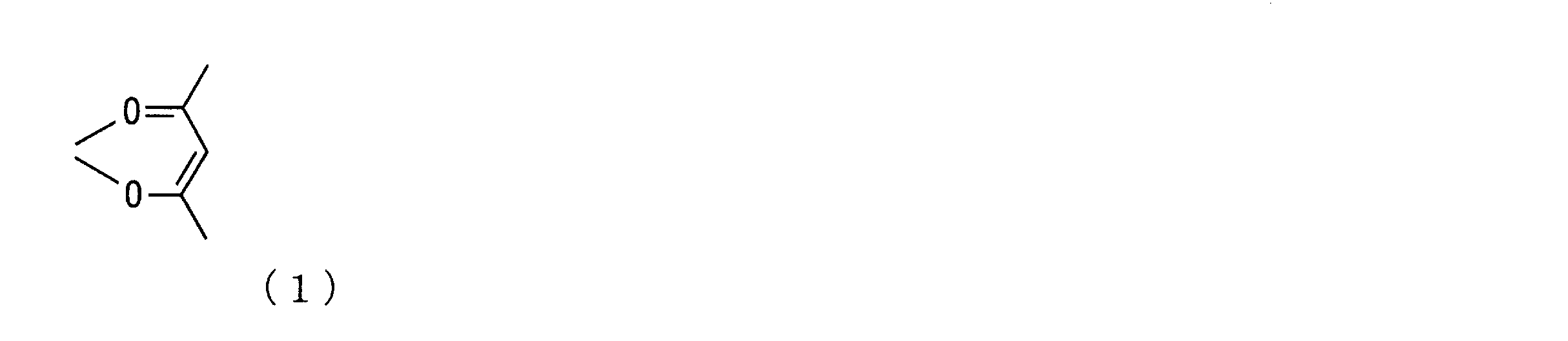
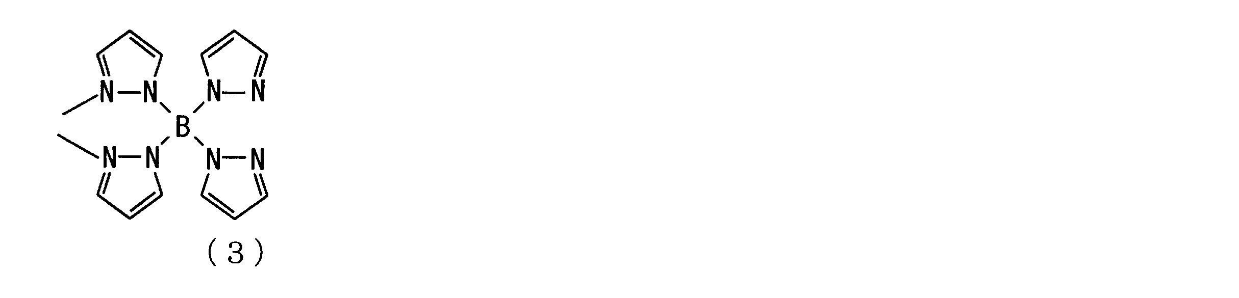
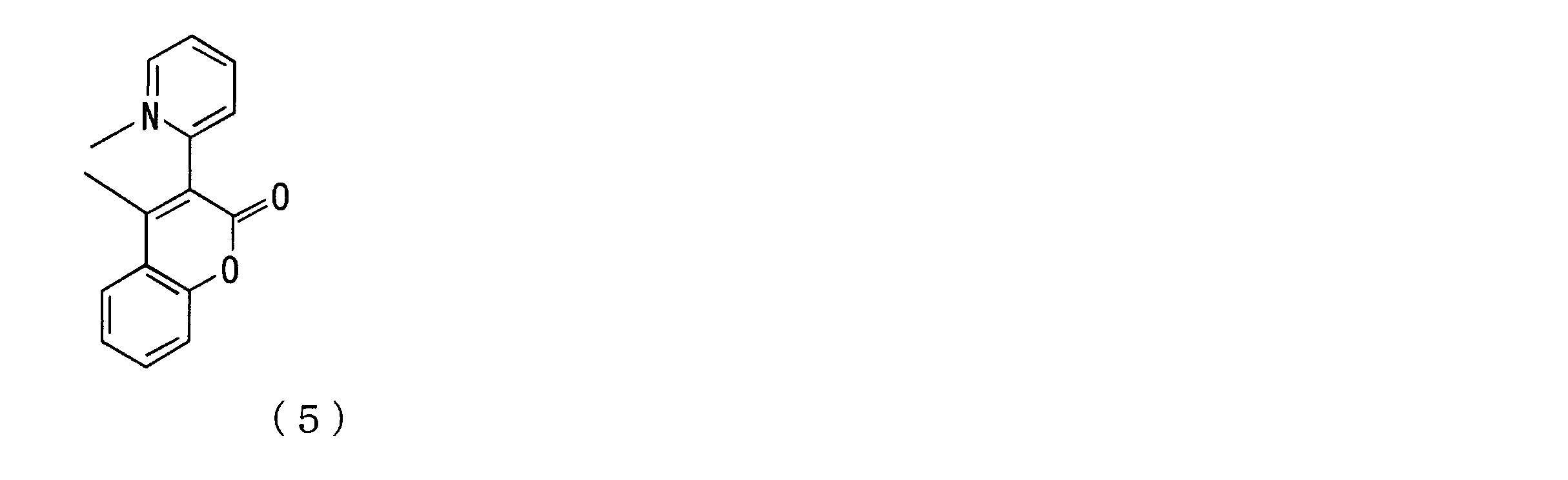
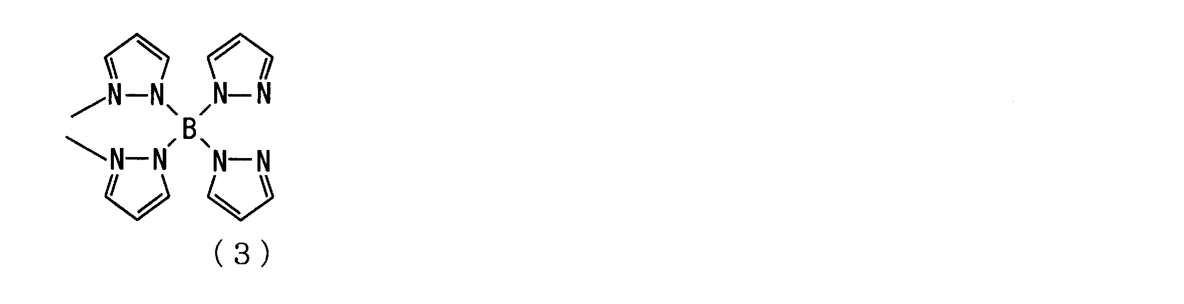
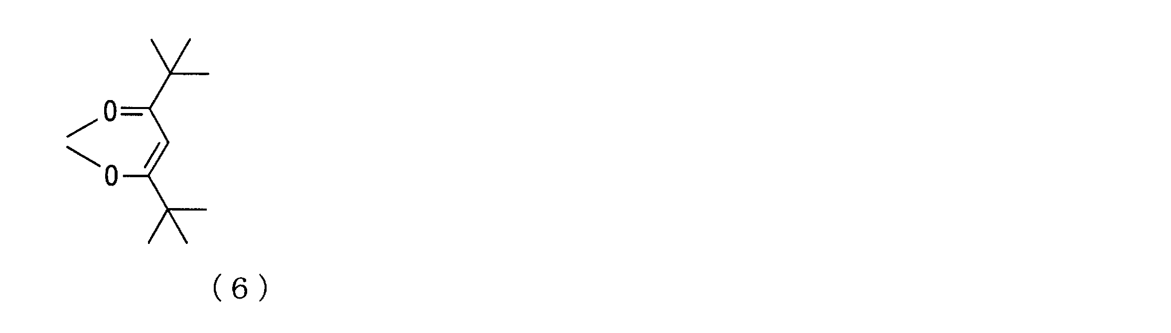
- the auxiliary ligand is acetyl acetate of a bidentate ligand of the following formula (1), and a carbon of a bidentate ligand of the following formula (2).
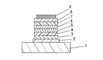
- each organic EL element of the organic EL panel according to the present embodiment As an example of each organic EL element of the organic EL panel according to the present embodiment, as shown in FIG. 1, a transparent anode 2, a hole injection layer 3, and a hole transport are sequentially formed on a transparent substrate 1 such as glass.
- the layer 4, the light emitting layer 5, the hole blocking layer 6, the electron transport layer 7, the electron injection layer 8, and a cathode 9 made of a metal are stacked to obtain.
- the hole injection layer 3, the hole transport layer 4, the light emitting layer 5, the hole blocking layer 6, and the electron transport layer 7 are organic material layers.
- a plurality of organic material layers stacked between a pair of opposing anodes and cathodes are a hole injection layer, a hole transport layer, a light emitting layer, a hole blocking layer, an electron transport layer, Includes an electron injection layer.
- Components such as the organic material layer will be described later.
- the anode 2 / hole injection layer 3 / light emitting layer 5 / electron transport layer 7 / electron injection layer 8 / cathode 9 / hole transport layer 4 and hole blocking layer 6 are omitted, although not shown,
- the anode 2 / hole transport layer 4 / light emitting layer 5 / electron transport layer 7 / electron injection layer 8 / cathode 9 / hole injection layer 3 and hole blocking layer 6 are omitted, and although not shown, the anode 2 A configuration in which the hole injection layer 3, the hole transport layer 4, and the hole blocking layer 6 of / light emitting layer 5 / electron transport layer 7 / electron injection layer 8 / cathode 9 / is omitted is also included in the present invention.
- the present invention is not limited to these stacked structures, and includes a structure including at least a light-emitting layer or a charge transport layer that can also be used.
- each organic EL element of the organic EL panel is an organic electroluminescent element provided with a plurality of organic material layers including a light emitting layer, which is laminated between a pair of opposed anodes and cathodes.
- At least one of the organic material layers is a layer formed by wet-coating and drying an organometallic complex composition described below.
- the hole injection layer and the hole transport layer may also be films formed and insolubilized by a wet coating method such as an inkjet method. There are other wet coating methods such as a spin coating method, a dip method, and a roll method, and even if these are used, a film can be formed with an organometallic complex composition.
- substrate As the substrate 1, a quartz or glass plate, a metal plate or a metal foil, a resin substrate to be bent, a plastic film, a sheet, or the like is used. In particular, a glass plate or a transparent synthetic resin plate such as polyester, polymethacrylate, polycarbonate, or polysulfone is preferable.
- a synthetic resin substrate it is necessary to pay attention to gas barrier properties. If the gas barrier property of the substrate is too small, the organic EL element may be deteriorated by the outside air that has passed through the substrate. For this reason, a method of providing a gas barrier property by providing a dense silicon oxide film or the like on at least one surface of the synthetic resin substrate is also a preferable method.
- the anode 2 that supplies holes to the layers up to the light emitting layer is usually a metal such as aluminum, gold, silver, nickel, palladium, platinum, or a metal such as indium and / or tin or zinc oxide (ITO or IZO). It is composed of an oxide, a metal halide such as copper iodide, carbon black, or a conductive polymer such as poly (3-methylthiophene), polypyrrole, or polyaniline.
- a metal such as aluminum, gold, silver, nickel, palladium, platinum, or a metal such as indium and / or tin or zinc oxide (ITO or IZO). It is composed of an oxide, a metal halide such as copper iodide, carbon black, or a conductive polymer such as poly (3-methylthiophene), polypyrrole, or polyaniline.
- the anode is usually formed by a sputtering method, a vacuum deposition method, or the like.
- an appropriate binder resin solution is used.
- the anode can also be formed by dispersing and coating the substrate.
- a conductive polymer a thin film can be directly formed on the substrate by electrolytic polymerization, or the anode can be formed by applying a conductive polymer on the substrate.
- the anode usually has a single-layer structure, but it can also have a laminated structure made of a plurality of materials if desired.
- the thickness of the anode depends on the required transparency. When transparency is required, the visible light transmittance is usually 60% or more, preferably 80% or more. In this case, the thickness of the anode is usually 5 nm or more, preferably 10 nm or more, and is usually 1000 nm or less, preferably about 500 nm or less. If it may be opaque, the thickness of the anode is arbitrary, and the anode may be integrated with the substrate 1. Furthermore, different conductive materials may be laminated.
- the anode surface is subjected to ultraviolet (UV) treatment or ozone treatment, oxygen plasma or argon plasma surface treatment, etc. It is preferable to do.
- UV ultraviolet
- ozone treatment oxygen plasma or argon plasma surface treatment, etc. It is preferable to do.
- a material used for the cathode 9 for supplying electrons to the layers up to the light emitting layer a material used for the anode can be used.
- a metal having a low work function is preferable.
- a suitable metal such as tin, magnesium, indium, calcium, aluminum, silver, or an alloy thereof is used.
- Specific examples include low work function alloy electrodes such as magnesium-silver alloy, magnesium-indium alloy, and aluminum-lithium alloy.
- the material of the cathode 9 only 1 type may be used for the material of the cathode 9, and 2 or more types may be used together by arbitrary combinations and a ratio.
- the thickness of the cathode is usually the same as that of the anode.
- a metal layer having a high work function and stable to the atmosphere because the stability of the device is increased.
- metals such as aluminum, silver, copper, nickel, chromium, gold, platinum are used.
- these materials may be used only by 1 type and may use 2 or more types together by arbitrary combinations and a ratio.
- the material and film thickness are selected so as to be transparent or translucent.
- Organic material layer The organic material layer constituting the main components of the hole injection layer 3, the hole transport layer 4, the light emitting layer 5, the electron transport layer 6 and the electron injection layer 7 has a charge transport property (hole and / or electron mobility).
- Examples of phosphorescent organometallic complex compounds used as the light-emitting layer 5 include Bis (3,5-difluoro-2- (2-pyridyl) phenyl- (2-carboxypyridyl) iridium III, Tris (2-phenylpyridine), which are iridium complexes.
- iridium (III) Bis (2-phenylbenzothiazolato) (acetylacetonate) iridium (III), Osmium (II) bis (3-trifluoromethyl-5- (2-pyridyl) -pyrazolate) dimethylphenylphosphine, a rare earth compound Tris (dibenzoylmethane) phenanthroline europium (III), platinum complex 2,3,7,8,12,13,17,18-Octaethyl-21H, 23H- porphine, platinum (II) And so on.
- organometallic complex compounds include central metals such as iridium, platinum, gold, and osmium, and (3,5-difluoro-2- (2-pyridyl) phenyl-, (2-phenylbenzothiazolato), and (3-trifluoromethyl-5
- a compound having an organic ligand such as-(2-pyridyl) -pyrazolate) and an auxiliary ligand such as (2-carboxypyridyl), (acetylacetonate) or dimethylphenylphosphine is preferably used. This is because the solubility in a solvent can be expected by introducing a group, etc.
- the organic metal complex compound having any one of skeletons of over bets available.
- Examples of the organic compound having an electron transporting property as a main component of the light emitting layer and the electron injection layer include polycyclic compounds such as p-terphenyl and quaterphenyl and derivatives thereof, naphthalene, tetracene, pyrene, coronene, chrysene, Condensed polycyclic hydrocarbon compounds such as anthracene, diphenylanthracene, naphthacene, phenanthrene and their derivatives, condensed heterocyclic compounds such as phenanthroline, bathophenanthroline, phenanthridine, acridine, quinoline, quinoxaline, phenazine and their derivatives, fluoro CEJN, perylene, phthaloperylene, naphthaloperylene, perinone, phthaloperinone, naphthaloperinone, diphenylbutadiene, tetraphenylbutadiene, oxadiazol
- metal chelate complex compounds particularly metal chelated oxanoid compounds, tris (8-quinolinolato) aluminum, bis (8-quinolinolato) magnesium, bis [benzo (f) -8-quinolinolato ] Zinc, bis (2-methyl-8-quinolinolato) (4-phenyl-phenolato) aluminum, tris (8-quinolinolato) indium, tris (5-methyl-8-quinolinolato) aluminum, 8-quinolinolatolithium, tris Mention may also be made of metal complexes having at least one 8-quinolinolato or a derivative thereof such as (5-chloro-8-quinolinolato) gallium and bis (5-chloro-8-quinolinolato) calcium as a ligand.
- metal complexes having at least one 8-quinolinolato or a derivative thereof such as (5-chloro-8-quinolinolato) gallium and bis (5-chloro-8-quino
- organic compounds having electron transport properties oxadiazoles, triazines, stilbene derivatives, distyrylarylene derivatives, styryl derivatives, and diolefin derivatives can also be suitably used.
- organic compound that can be used as an organic compound having an electron transporting property 2,5-bis (5,7-di-t-benzyl-2-benzoxazolyl) -1,3,4-thiazole, 4, 4'-bis (5,7-t-pentyl-2-benzoxazolyl) stilbene, 4,4'-bis [5,7-di- (2-methyl-2-butyl) -2-benzoxazoly Ru] stilbene, 2,5-bis (5.7-di-t-pentyl-2-benzoxazolyl) thiophene, 2,5-bis [5- ( ⁇ , ⁇ -dimethylbenzyl) -2-benzoxa Zolyl] thiophene, 2,5-bis [5,7-di- (2-methyl-2-butyl) -2-benzoxazolyl] -3,4-diphenylthiophene, 2,5-bis (5- Methyl-2-benzoxazolyl) thiophene, 4,
- 1,4-bis (2-methylstyryl) benzene 1,4-bis (3-methylstyryl) benzene, 1,4-bis (4-methylstyryl) benzene, Distyrylbenzene, 1,4-bis (2-ethylstyryl) benzene, 1,4-bis (3-ethylstyryl) benzene, 1,4-bis (2-methylstyryl) -2-methylbenzene, 1,4 There may also be mentioned -bis (2-methylstyryl) -2-ethylbenzene.
- organic compound having an electron transporting property 2,5-bis (4-methylstyryl) pyrazine, 2,5-bis (4-ethylstyryl) pyrazine, 2,5-bis [2- (1- Naphthyl) vinyl] pyrazine, 2,5-bis (4-methoxystyryl) pyrazine, 2,5-bis [2- (4-biphenyl) vinyl] pyrazine, 2,5-bis [2- (1-pyrenyl) vinyl ] Pyrazine etc. are mentioned.
- organic compounds having electron transport properties include 1,4-phenylene dimethylidin, 4,4'-phenylene dimethylidin, 2,5-xylylene dimethylidin, and 2,6-naphthylene dimethylidene. Din, 1,4-biphenylenedimethylidin, 1,4-p-terephenylenedimethylidin, 9,10-anthracenediyldimethylidin, 4,4 '-(2,2-di-t-butylphenylvinyl
- Well-known ones conventionally used for producing organic EL devices such as biphenyl and 4,4 ′-(2,2-diphenylvinyl) biphenyl, can be appropriately used.
- organic compounds having hole transporting properties include N, N, N ′, N′-tetraphenyl-4,4′-diaminophenyl, N, N′-diphenyl-N, N′-di (3-methyl Phenyl) -4,4′-diaminobiphenyl, 2,2-bis (4-di-p-tolylaminophenyl) propane, N, N, N ′, N′-tetra-p-tolyl-4,4′- Diaminobiphenyl, bis (4-di-p-tolylaminophenyl) phenylmethane, N, N′-diphenyl-N, N′-di (4-methoxyphenyl) -4,4′-diaminobiphenyl, N, N, N ′, N′-tetraphenyl-4,4′-diaminodiphenyl ether, 4,4′-bis (diphenylamino) quadriphenyl
- the hole injection layer, the hole transport layer, and the hole transport light emitting layer those obtained by dispersing the above organic compound in a polymer or those polymerized can be used.
- So-called ⁇ -conjugated polymers such as polyparaphenylene vinylene and derivatives thereof, hole-transporting non-conjugated polymers represented by poly (N-vinylcarbazole), and sigma-conjugated polymers of polysilanes can also be used.
- the hole injection layer is not particularly limited, but metal phthalocyanines such as copper phthalocyanine (CuPc: Copper Phthalocyanine) and metal-free phthalocyanines, carbon films, and conductive polymers such as polyaniline can be suitably used.
- metal phthalocyanines such as copper phthalocyanine (CuPc: Copper Phthalocyanine) and metal-free phthalocyanines, carbon films, and conductive polymers such as polyaniline can be suitably used.
- FIrPic Bis (2,4-difluorophenylpyridinato) (2-carboxypyridyl) iridium (III)
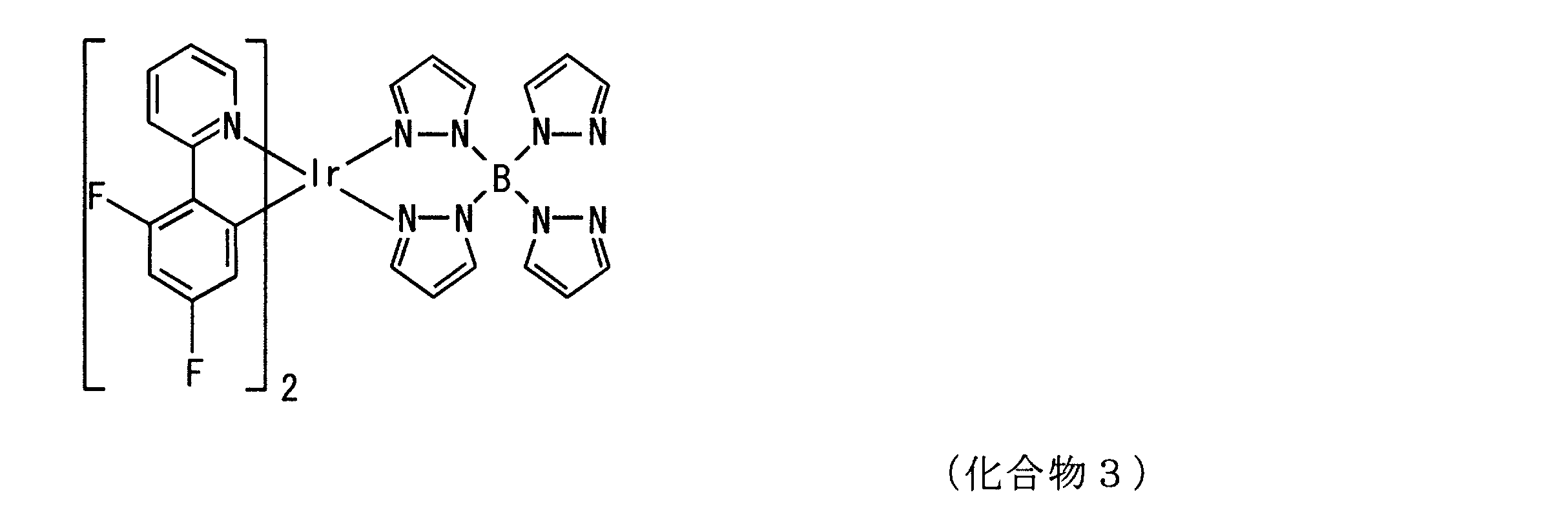
- FIr6 Bis (2,4-difluorophenylpyridinato) tetrakis (1-pyrazolyl) borate iridium (III)
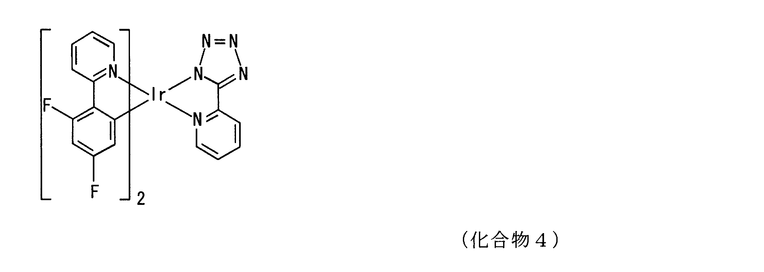
- FIrN4 Bis (4,6-difluorophenylpyridinato) (5- (pyridin-2-yl) -tetrazolate) iridium (III)
- Hex-Ir (phq) 2acac Bis [2- (4-n-hexylphenyl) quinoline)] (acetylacetonate) iridium (III)
- the prepared coating liquid was held for 10 minutes to 60 minutes on a hot plate heated to 200 ° C. to 230 ° C. and observed. Thereafter, the presence or absence of light emission was confirmed with a 365 nm handy UV lamp.
- Table 2 shows the results of the luminescence experiment together with the boiling point of the solvent and the polarity factor. The presence or absence of light emission is indicated by ⁇ and the absence is indicated by ⁇ .
- an aprotic solvent means a solvent having a molecular structure in which there is no structure in which only one hydrogen group is bonded to a tertiary carbon atom of the carbon skeleton, and which does not dissociate under heating conditions to generate a proton (H +). To do.
- a solvent for the metal complex composition dodecylbenzene, tetralin, 1,5-dimethyltetralin, methyl benzoate, ethyl benzoate, isopropyl benzoate, butyl benzoate, benzyl benzoate, 2-phenoxyethyl acetate, and aprotic of diphenyl ether A solvent was preferred.
- PEDOT PSS (poly (3,4-ethylenedioxythiophene): poly (styrenesulfonate) poly (3,4) as a hole injection / transport layer in order by vacuum deposition on a glass substrate on which a transparent electrode ITO is formed as an anode.
- PSS poly (3,4-ethylenedioxythiophene): poly (styrenesulfonate) poly (3,4) as a hole injection / transport layer in order by vacuum deposition on a glass substrate on which a transparent electrode ITO is formed as an anode.
- 4-ethylenedioxythiophene poly (styrenesulfonate)) was formed to a thickness of 32 nm.
- the laminated structure of the element is anode / hole injection / transport layer / light emitting layer / electron transport layer / electron injection layer / cathode in this order: ITO / PEDOT: PSS / Ir (2-phq) 2 (acac): 26DCzPPy / Alq3 / Li 2 O / Al. Regardless of the heating at 200 ° C., all the elements were able to confirm red light emission.
- Example of this invention was described by the organic EL element, this invention is not limited to these Examples.
Landscapes
- Chemical & Material Sciences (AREA)
- Engineering & Computer Science (AREA)
- Materials Engineering (AREA)
- Crystallography & Structural Chemistry (AREA)
- Inorganic Chemistry (AREA)
- Organic Chemistry (AREA)
- Electroluminescent Light Sources (AREA)
Abstract
【課題】溶媒及び有機EL材料の選択性を向上し、耐熱性のある有機電界発光素子用金属錯体組成物を提供する。 【解決手段】有機電界発光素子用金属錯体組成物は、中心金属、有機配位子及び補助配位子を有する発光性有機金属錯体とアプロチック溶媒とを含む。
Description
本発明は、有機材料層に有機金属錯体化合物を利用した有機電界発光素子に関し、特に、有機エレクトロルミネッセンス(EL)素子に用いる金属錯体組成物に関する。
一般に、有機EL素子は複数の有機材料層を積層した構造を有している。有機材料層には、発光層の他に、正孔注入層、正孔輸送層などの正孔輸送能を持つ材料からなる層や、電子輸送層、電子注入層などの電子輸送能を持つ材料からなる層などが含まれる。
発光層並びに電子或いは正孔の輸送層の積層体の有機EL膜に電界が印加されると、陽極からは正孔が、陰極からは電子が注入され、これらが発光層において再結合し励起子が形成され、基底状態に戻るとき発光する。発光効率を向上させるためには、電子などのキャリアを効率よく界面に輸送することが重要で、有機EL素子でも電荷輸送性を有する有機化合物を利用した多層構造を有している。有機化合物において励起状態の種類として、一重項励起状態からの発光が蛍光、三重項励起状態からの発光が燐光があり、発光効率の観点から燐光材料が注目されている。発光層に用いられる燐光材料の多くは重原子を含む金属錯体である。
このような有機発光素子の分野において、有機ELパネルの製造方法では、より低コスト化された生産方法の確立のために、湿式塗布により膜形成を実施する採用が増えてきている。湿式塗布方式としては、たとえばスピン法、ディップ法、ロール法、インクジェット法などの方式がある。微細かつ容易にパターニングができるインクジェット方式が注目されている。
インクジェット法を用いて基板上にて有機EL素子ごとの発光層や有機材料層を塗り分ける際、所望の低分子化合物を混合した塗布液体(インク)の溶媒は200℃程度の高沸点のものを使用することが提案されている(特許文献1参照)。これは揮発に伴う射出ヘッドの低分子化合物の目詰まり対策のためである。
この他にインク固形分の溶解性の向上や析出を押さえるため、極性が高い溶媒を使用することも提案されている。
しかしながら、従来の湿式塗布方式の有機電界発光素子の製造方法において、塗布液体に使用できる溶媒及び有機EL材料の選択の種々制限されていた。
そこで、本発明は、塗布液体(インク)に使用できる溶媒及び有機EL材料の選択性を高め、耐熱性のある有機電界発光素子の製造方法に用いられる金属錯体組成物を提供することを課題の一例としてあげられる。
本発明者は、上記課題を解決すべく鋭意検討した結果、湿式塗布方式で有機EL素子を製造した場合、有機金属錯体を含む塗布液の溶媒に起因して当該有機金属錯体の発光層の発光が消光することを知見した。そこで、特定の有機材料及び溶媒の分子構造を特定化することで、使用できる材料の選択性を向上させる効果が得られることが判り、本発明の完成に至った。
本発明による有機電界発光素子用金属錯体組成物は、中心金属、有機配位子及び補助配位子を有する発光性有機金属錯体とアプロチック溶媒(aprotic solvent)とを含有することを特徴とする。
本発明による上記有機電界発光素子用金属錯体組成物においては、アプロチック溶媒は炭素骨格の第3級炭素原子に水素基が1つのみ結合した構造が存在しない分子構造を有する非プロトン性極性溶媒の群から選択されることとすることができる。これにより、当該金属錯体組成物が発光層に利用される場合、当該発光層の消光が防止される。
本発明による上記有機電界発光素子用金属錯体組成物においては、アプロチック溶媒は沸点が200℃以上である非プロトン性極性溶媒の群から選択されることとすることができる。これにより、インクジェット法を用いて有機材料層を塗り分ける際、射出ヘッドの当該金属錯体組成物の目詰まりを防止できる。
本発明による上記有機電界発光素子用金属錯体組成物においては、アプロチック溶媒はハロゲン基が含有されてない分子構造を有する非プロトン性極性溶媒の群から選択されることとすることができる。これにより、当該金属錯体組成物が発光層に利用される場合、当該発光層の消光が防止される。
本発明による上記有機電界発光素子用金属錯体組成物においては、アプロチック溶媒はドデシルベンゼン、テトラリン、1,5-ジメチルテトラリン、安息香酸メチル、安息香酸エチル、安息香酸イソプロピル、安息香酸ブチル、安息香酸ベンジル、酢酸2-フェノキシエチル、ジフェニルエーテル、ドデシルベンゼン及びそれらの組合せから成る群から選択されることとすることができる。これにより、当該金属錯体組成物が発光層に利用される場合、当該発光層の消光が防止される。
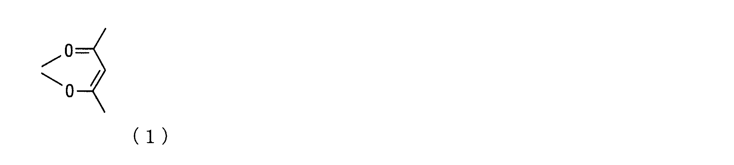
本発明による上記有機電界発光素子用金属錯体組成物においては、前記補助配位子は下記(1)式の二座配位子のアセチルアセテート、下記(2)式の二座配位子のカーボキシピリジル、下記(3)式の二座配位子のピラゾール-ボロネート、下記(4)式の二座配位子のピラジン-テトラゾロネート、下記(5)式の二座配位子のピリジンクロメンネート、下記(6)式の二座配位子のテトラメチルへプタンジネートのいずれか1つの骨格を有することとすることができる。これにより、当該金属錯体組成物の溶媒への溶解性向上が期待される。



以下に本発明による実施の形態を図面を参照しつつ説明する。
[有機EL素子]
本実施形態による有機ELパネルの各有機EL素子の一例としては、図1に示すように、ガラスなどの透明基板1上にて、順に、透明な陽極2、正孔注入層3、正孔輸送層4、発光層5、正孔阻止層6、電子輸送層7、電子注入層8及び金属からなる陰極9が積層されて得られるものが挙げられる。正孔注入層3、正孔輸送層4、発光層5、正孔阻止層6、及び電子輸送層7は有機材料層である。すなわち、有機EL素子において、対向する1対の陽極及び陰極の間に積層配置された複数の有機材料層が正孔注入層、正孔輸送層、発光層、正孔阻止層、電子輸送層、電子注入層を包含する。これら有機材料層などの構成要素について後述する。
本実施形態による有機ELパネルの各有機EL素子の一例としては、図1に示すように、ガラスなどの透明基板1上にて、順に、透明な陽極2、正孔注入層3、正孔輸送層4、発光層5、正孔阻止層6、電子輸送層7、電子注入層8及び金属からなる陰極9が積層されて得られるものが挙げられる。正孔注入層3、正孔輸送層4、発光層5、正孔阻止層6、及び電子輸送層7は有機材料層である。すなわち、有機EL素子において、対向する1対の陽極及び陰極の間に積層配置された複数の有機材料層が正孔注入層、正孔輸送層、発光層、正孔阻止層、電子輸送層、電子注入層を包含する。これら有機材料層などの構成要素について後述する。
図1に示す陽極2/正孔注入層3/正孔輸送層4/発光層5/正孔阻止層6/電子輸送層7/電子注入層8/陰極9/の構成の他に、図示しないが、陽極2/正孔注入層3/発光層5/電子輸送層7/電子注入層8/陰極9/の正孔輸送層4、正孔阻止層6を省いた構成や、図示しないが、陽極2/正孔輸送層4/発光層5/電子輸送層7/電子注入層8/陰極9/の正孔注入層3、正孔阻止層6を省いた構成や、図示しないが、陽極2/発光層5/電子輸送層7/電子注入層8/陰極9/の正孔注入層3、正孔輸送層4、正孔阻止層6を省いた構成も本発明に含まれる。また、以上説明した層構成において、基板以外の構成要素を逆の順に積層することも可能である。いずれにしても、これら積層構成に限定されることなく、少なくとも発光層を含み、或いは兼用できる電荷輸送層を含む構成は本発明に含まれる。
このように有機ELパネルの各有機EL素子は、対向する1対の陽極及び陰極の間に積層配置されかつ発光層を含む複数の有機材料層を備えた有機電界発光素子である。そして、有機材料層の少なくとも1層、例えば少なくとも発光層は、後述する有機金属錯体組成物が湿式塗布され乾燥して形成された層である。なお、正孔注入層、正孔輸送層も、インクジェット法など湿式塗布方法にて成膜され不溶化された膜であり得る。なお、湿式塗布方法は他に、スピンコート方法、ディップ法、ロール法があり、これらを用いても有機金属錯体組成物により成膜できる。
[基板]
基板1としては、石英やガラスの板、金属板や金属箔、曲げられる樹脂基板、プラスチックフィルムやシートなどが用いられる。特にガラス板や、ポリエステル、ポリメタクリレート、ポリカーボネート、ポリスルホンなどの透明な合成樹脂の板が好ましい。合成樹脂基板を使用する場合にはガスバリア性に留意する必要がある。基板のガスバリア性が小さすぎると、基板を通過した外気により有機EL素子が劣化することがあるので好ましくない。このため、合成樹脂基板の少なくとも片面に緻密なシリコン酸化膜などを設けてガスバリア性を確保する方法も好ましい方法の一つである。
基板1としては、石英やガラスの板、金属板や金属箔、曲げられる樹脂基板、プラスチックフィルムやシートなどが用いられる。特にガラス板や、ポリエステル、ポリメタクリレート、ポリカーボネート、ポリスルホンなどの透明な合成樹脂の板が好ましい。合成樹脂基板を使用する場合にはガスバリア性に留意する必要がある。基板のガスバリア性が小さすぎると、基板を通過した外気により有機EL素子が劣化することがあるので好ましくない。このため、合成樹脂基板の少なくとも片面に緻密なシリコン酸化膜などを設けてガスバリア性を確保する方法も好ましい方法の一つである。
[陽極及び陰極]
発光層までの層に正孔を供給する陽極2は、通常、アルミニウム、金、銀、ニッケル、パラジウム、白金などの金属、インジウム及び/又はスズ、亜鉛の酸化物(ITOやIZO)などの金属酸化物、ヨウ化銅などのハロゲン化金属、カーボンブラック、或いは、ポリ(3-メチルチオフェン)、ポリピロール、ポリアニリンなどの導電性高分子などにより構成される。
発光層までの層に正孔を供給する陽極2は、通常、アルミニウム、金、銀、ニッケル、パラジウム、白金などの金属、インジウム及び/又はスズ、亜鉛の酸化物(ITOやIZO)などの金属酸化物、ヨウ化銅などのハロゲン化金属、カーボンブラック、或いは、ポリ(3-メチルチオフェン)、ポリピロール、ポリアニリンなどの導電性高分子などにより構成される。
陽極の形成は通常、スパッタリング法、真空蒸着法などにより行われることが多い。また、銀などの金属微粒子、ヨウ化銅などの微粒子、カーボンブラック、導電性の金属酸化物微粒子、導電性高分子微粉末などを用いて陽極を形成する場合には、適当なバインダー樹脂溶液に分散させて、基板上に塗布することにより陽極を形成することもできる。さらに、導電性高分子の場合は、電解重合により直接基板上に薄膜を形成したり、基板上に導電性高分子を塗布して陽極を形成することもできる。
陽極は通常は単層構造であるが、所望により複数の材料からなる積層構造とすることも可能である。
陽極の厚みは、必要とする透明性により異なる。透明性が必要とされる場合は、可視光の透過率を、通常60%以上、好ましくは80%以上とすることが好ましい。この場合、陽極の厚みは通常5nm以上、好ましくは10nm以上であり、また、通常1000nm以下、好ましくは500nm以下程度である。不透明でよい場合は陽極の厚みは任意であり、陽極は基板1と一体化されたものであってもよい。また、さらには、異なる導電材料が積層されたものであってもよい。
陽極に付着した不純物を除去し、イオン化ポテンシャルを調整して正孔注入性を向上させることを目的に、陽極表面を紫外線(UV)処理又はオゾン処理したり、酸素プラズマ又はアルゴンプラズマ表面処理したりすることが好ましい。
発光層までの層に電子を供給する陰極9の材料としては、陽極に使用される材料を用いることが可能であるが、効率良く電子注入を行うには、仕事関数の低い金属が好ましく、たとえば、スズ、マグネシウム、インジウム、カルシウム、アルミニウム、銀などの適当な金属又はそれらの合金が用いられる。具体例としては、マグネシウム-銀合金、マグネシウム-インジウム合金、アルミニウム-リチウム合金などの低仕事関数合金電極が挙げられる。
なお、陰極9の材料は、1種のみを用いてもよく、2種以上を任意の組み合わせ及び比率で併用してもよい。陰極の膜厚は、通常、陽極と同様である。
さらに、低仕事関数金属から成る陰極を保護する目的で、この上に更に、仕事関数が高く大気に対して安定な金属層を積層すると、素子の安定性が増すので好ましい。この目的のために、たとえば、アルミニウム、銀、銅、ニッケル、クロム、金、白金などの金属が使われる。なお、これらの材料は、1種のみで用いてもよく、2種以上を任意の組み合わせ及び比率で併用してもよい。
さらに、陽極及び陰極は、発光の取り出し側となる場合は、透明又は半透明となるように材料、膜厚を選択する。特に陽極及び陰極のうちどちらか、もしくはその両方が、有機発光材料から得られる発光波長において少なくとも10%以上の透過率を持つ材料を選択することが好ましい。これら電極は、必要に応じてパターニングしても良い。
[有機材料層]
正孔注入層3、正孔輸送層4、発光層5、電子輸送層6及び電子注入層7の主成分を構成する有機材料層は、電荷輸送性(正孔及び/又は電子の移動性)を有する有機化合物を利用する。
正孔注入層3、正孔輸送層4、発光層5、電子輸送層6及び電子注入層7の主成分を構成する有機材料層は、電荷輸送性(正孔及び/又は電子の移動性)を有する有機化合物を利用する。
発光層5として用いられる燐光性の有機金属錯体化合物としては、イリジウム錯体であるBis (3,5-difluoro-2- (2-pyridyl) phenyl- (2-carboxypyridyl) iridium III、Tris (2-phenylpyridine) iridium(III)、Bis (2-phenylbenzothiazolato) (acetylacetonate) iridium(III)、オスミウム錯体であるOsmium(II) bis(3-trifluoromethyl -5-(2-pyridyl) -pyrazolate)dimethylphenylphosphine、希土類化合物のTris (dibenzoylmethane) phenanthroline europium(III)、白金錯体である2,3,7,8,12,13,17,18-Octaethyl-21H, 23H- porphine,platinum(II)
などを挙げることができる。特に、有機金属錯体化合物は、イリジウム、白金、金、オスミウムなどの中心金属と、(3,5-difluoro-2- (2-pyridyl) phenyl-や(2-phenylbenzothiazolato)や(3-trifluoromethyl -5-(2-pyridyl) -pyrazolate)などの有機配位子と、(2-carboxypyridyl)や(acetylacetonate)やdimethylphenylphosphineなどの補助配位子を有するものが好ましく用いられる。かかる補助配位子へのアルキル基などの導入により、溶媒への溶解性向上が期待できるからである。補助配位子として上記(1)式の二座配位子のアセチルアセテート、上記(2)式の二座配位子のカーボキシピリジル、上記(3)式の二座配位子のピラゾール-ボロネート、上記(4)式の二座配位子のピラジン-テトラゾロネート、上記(5)式の二座配位子のピリジンクロメンネート、上記(6)式の二座配位子のテトラメチルへプタンジネートのいずれか1つの骨格を有する有機金属錯体化合物が利用できる。
などを挙げることができる。特に、有機金属錯体化合物は、イリジウム、白金、金、オスミウムなどの中心金属と、(3,5-difluoro-2- (2-pyridyl) phenyl-や(2-phenylbenzothiazolato)や(3-trifluoromethyl -5-(2-pyridyl) -pyrazolate)などの有機配位子と、(2-carboxypyridyl)や(acetylacetonate)やdimethylphenylphosphineなどの補助配位子を有するものが好ましく用いられる。かかる補助配位子へのアルキル基などの導入により、溶媒への溶解性向上が期待できるからである。補助配位子として上記(1)式の二座配位子のアセチルアセテート、上記(2)式の二座配位子のカーボキシピリジル、上記(3)式の二座配位子のピラゾール-ボロネート、上記(4)式の二座配位子のピラジン-テトラゾロネート、上記(5)式の二座配位子のピリジンクロメンネート、上記(6)式の二座配位子のテトラメチルへプタンジネートのいずれか1つの骨格を有する有機金属錯体化合物が利用できる。
また、発光層や電子注入層の主成分の電子輸送性を有する有機化合物としては、p-テルフェニルやクアテルフェニルなどの多環化合物及びそれらの誘導体、ナフタレン、テトラセン、ピレン、コロネン、クリセン、アントラセン、ジフェニルアントラセン、ナフタセン、フェナントレンなどの縮合多環炭化水素化合物及びそれらの誘導体、フェナントロリン、バソフェナントロリン、フェナントリジン、アクリジン、キノリン、キノキサリン、フェナジンなどの縮合複素環化合物及びそれらの誘導体や、フルオロセイン、ペリレン、フタロペリレン、ナフタロペリレン、ペリノン、フタロペリノン、ナフタロペリノン、ジフェニルブタジエン、テトラフェニルブタジエン、オキサジアゾール、アルダジン、ビスベンゾキサゾリン、ビススチリル、ピラジン、シクロペンタジエン、オキシン、アミノキノリン、イミン、ジフェニルエチレン、ビニルアントラセン、ジアミノカルバゾール、ピラン、チオピラン、ポリメチン、メロシアニン、キナクリドン、ルブレンなど及びそれらの誘導体などを挙げることができる。
さらに、電子輸送性を有する有機化合物として、金属キレート錯体化合物、特に金属キレート化オキサノイド化合物では、トリス(8-キノリノラト)アルミニウム、ビス(8-キノリノラト)マグネシウム、ビス[ベンゾ(f)-8-キノリノラト]亜鉛、ビス(2-メチル-8-キノリノラト)(4-フェニル-フェノラト)アルミニウム、トリス(8-キノリノラト)インジウム、トリス(5-メチル-8-キノリノラト)アルミニウム、8-キノリノラトリチウム、トリス(5-クロロ-8-キノリノラト)ガリウム、ビス(5-クロロ-8-キノリノラト)カルシウムなどの8-キノリノラト或いはその誘導体を配位子として少なくとも一つ有する金属錯体も挙げることができる。
また、電子輸送性を有する有機化合物として、オキサジアゾール類、トリアジン類、スチルベン誘導体及びジスチリルアリーレン誘導体、スチリル誘導体、ジオレフィン誘導体も好適に使用され得る。
さらに、電子輸送性を有する有機化合物として使用できる有機化合物として、2,5-ビス(5,7-ジ-t-ベンチル-2-ベンゾオキサゾリル)-1,3,4-チアゾール、4,4’-ビス(5,7-t-ペンチル-2-ベンゾオキサゾリル)スチルベン、4,4’-ビス[5,7-ジ-(2-メチル-2-ブチル)-2-ベンゾオキサゾリル]スチルベン、2,5-ビス(5.7-ジ-t-ペンチル-2-ベンゾオキサゾリル)チオフェン、2,5-ビス[5-(α,α-ジメチルベンジル)-2-ベンゾオキサゾリル]チオフェン、2,5-ビス[5,7-ジ-(2-メチル-2-ブチル)-2-ベンゾオキサゾリル]-3,4-ジフェニルチオフェン、2,5-ビス(5-メチル-2-ベンゾオキサゾリル)チオフェン、4,4’-ビス(2-ベンゾオキサゾリル)ビフェニル、5-メチル-2-{2-[4-(5-メチル-2-ベンゾオキサゾリル)フェニル]ビニル}ベンゾオキサゾール、2-[2-(4-クロロフェニル)ビニル]ナフト(1,2-d)オキサゾールなどのベンゾオキサゾール系、2,2’-(p-フェニレンジピニレン)-ビスベンゾチアゾールなどのベンゾチアゾール系、2-{2-[4-(2-ベンゾイミダゾリル)フェニル〕ビニル}ベンゾイミダゾール、2-[2-(4-カルボキシフェニル)ビニル]ベンゾイミダゾールなども挙げられる。
さらに、電子輸送性を有する有機化合物として、1,4-ビス(2-メチルスチリル)ベンゼン、1,4-ビス(3-メチルスチリル)ベンゼン、1,4-ビス(4-メチルスチリル)ベンゼン、ジスチリルベンゼン、1,4-ビス(2-エチルスチリル)ベンゼン、1,4-ビス(3-エチルスチリル)ベンゼン、1,4-ビス(2-メチルスチリル)-2-メチルベンゼン、1,4-ビス(2-メチルスチリル)-2-エチルベンゼンなども挙げられる。
また、さらに、電子輸送性を有する有機化合物として、2,5-ビス(4-メチルスチリル)ピラジン、2,5-ビス(4-エチルスチリル)ピラジン、2,5-ビス[2-(1-ナフチル)ビニル]ピラジン、2,5-ビス(4-メトキシスチリル)ピラジン、2,5-ビス[2-(4-ビフェニル)ビニル]ピラジン、2,5-ビス[2-(1-ピレニル)ビニル]ピラジンなどが挙げられる。
その他、さらに、電子輸送性を有する有機化合物として、1,4-フェニレンジメチリディン、4,4’-フェニレンジメチリディン、2,5-キシリレンジメチリディン、2,6-ナフチレンジメチリディン、1,4-ビフェニレンジメチリディン、1,4-p-テレフェニレンジメチリディン、9,10-アントラセンジイルジメチリディン、4,4’-(2,2-ジ-t-ブチルフェニルビニル)ビフェニル、4,4’-(2,2-ジフェニルビニル)ビフェニルなど、従来有機EL素子の作製に使用されている公知のものを適宜用いることができる。
一方、正孔輸送性を有する有機化合物として、N,N,N’,N’-テトラフェニル-4,4’-ジアミノフェニル、N,N’-ジフェニル-N,N’-ジ(3-メチルフェニル)-4,4’-ジアミノビフェニル、2,2-ビス(4-ジ-p-トリルアミノフェニル)プロパン、N,N,N’,N’-テトラ-p-トリル-4,4’-ジアミノビフェニル、ビス(4-ジ-p-トリルアミノフェニル)フェニルメタン、N,N’-ジフェニル-N,N’-ジ(4-メトキシフェニル)-4,4’-ジアミノビフェニル、N,N,N’,N’-テトラフェニル-4,4’-ジアミノジフェニルエーテル、4,4’-ビス(ジフェニルアミノ)クオードリフェニル、4-N,N-ジフェニルアミノ-(2-ジフェニルビニル)ベンゼン、3-メトキシ-4’-N,N-ジフェニルアミノスチルベンゼン、N-フェニルカルバゾール、1,1-ビス(4-ジ-p-トリアミノフェニル)-シクロヘキサン、1,1-ビス(4-ジ-p-トリアミノフェニル)-4-フェニルシクロヘキサン、ビス(4-ジメチルアミノ-2-メチルフェニル)-フェニルメタン、N,N,N-トリ(p-トリル)アミン、4-(ジ-p-トリルアミノ)-4’-[4(ジ-p-トリルアミノ)スチリル]スチルベン、N,N,N’,N’-テトラ-p-トリル-4,4’-ジアミノ-ビフェニル、N,N,N’,N’-テトラフェニル-4,4’-ジアミノ-ビフェニルN-フェニルカルバゾール、4,4’-ビス[N-(1-ナフチル)-N-フェニル-アミノ]ビフェニル、4,4’’-ビス[N-(1-ナフチル)-N-フェニル-アミノ]p-ターフェニル、4,4’-ビス[N-(2-ナフチル)-N-フェニル-アミノ]ビフェニル、4,4’-ビス[N-(3-アセナフテニル)-N-フェニル-アミノ]ビフェニル、1,5-ビス[N-(1-ナフチル)-N-フェニル-アミノ]ナフタレン、4,4’-ビス[N-(9-アントリル)-N-フェニル-アミノ]ビフェニル、4,4’’-ビス[N-(1-アントリル)-N-フェニル-アミノ]p-ターフェニル、4,4’-ビス[N-(2-フェナントリル)-N-フェニル-アミノ]ビフェニル、4,4’-ビス[N-(8-フルオランテニル)-N-フェニル-アミノ]ビフェニル、4,4’-ビス[N-(2-ピレニル)-N-フェニル-アミノ]ビフェニル、4,4’-ビス[N-(2-ペリレニル)-N-フェニル-アミノ]ビフェニル、4,4’-ビス[N-(1-コロネニル)-N-フェニル-アミノ]ビフェニル、2,6-ビス(ジ-p-トリルアミノ)ナフタレン、2,6-ビス[ジ-(1-ナフチル)アミノ]ナフタレン、2,6-ビス[N-(1-ナフチル)-N-(2-ナフチル)アミノ]ナフタレン、4.4’’-ビス[N,N-ジ(2-ナフチル)アミノ]ターフェニル、4.4’-ビス{N-フェニル-N-[4-(1-ナフチル)フェニル]アミノ}ビフェニル、4,4’-ビス[N-フェニル-N-(2-ピレニル)-アミノ]ビフェニル、2,6-ビス[N,N-ジ(2-ナフチル)アミノ]フルオレン、4,4’’-ビス(N,N-ジ-p-トリルアミノ)ターフェニル、ビス(N-1-ナフチル)(N-2-ナフチル)アミンなどが挙げられる。
さらに、正孔注入層、正孔輸送層、正孔輸送性発光層として、上述の有機化合物をポリマ中に分散したものや、ポリマ化したものも使用できる。ポリパラフェニレンビニレンやその誘導体などのいわゆるπ共役ポリマ、ポリ(N-ビニルカルバゾール)に代表される正孔輸送性非共役ポリマ、ポリシラン類のシグマ共役ポリマも用いることができる。
正孔注入層としては、特に限定はないが、銅フタロシアニン(CuPc:Copper Phthalocyanine)などの金属フタロシアニン類及び無金属フタロシアニン類、カーボン膜、ポリアニリンなどの導電性ポリマが好適に使用できる。
--湿式塗布方式に適した金属錯体組成物--
金属錯体組成物の試験のために以下の溶質(有機金属錯体)と溶媒(極性溶媒(プロトン性溶媒、非プロトン性溶媒)、無極性溶媒)とを用意した。
[溶質](Luminescence Technology社製)
Ir(ppy)2(acac) : Bis(2-phenylpyridine)(acetylacetonate)iridium(III)
金属錯体組成物の試験のために以下の溶質(有機金属錯体)と溶媒(極性溶媒(プロトン性溶媒、非プロトン性溶媒)、無極性溶媒)とを用意した。
[溶質](Luminescence Technology社製)
Ir(ppy)2(acac) : Bis(2-phenylpyridine)(acetylacetonate)iridium(III)

FIrPic : Bis(2,4-difluorophenylpyridinato) (2-carboxypyridyl)iridium (III)

FIr6 : Bis(2,4-difluorophenylpyridinato)tetrakis(1-pyrazolyl)borate iridium (III)
FIrN4 : Bis(4,6-difluorophenylpyridinato)(5-(pyridin-2-yl)-tetrazolate) iridium (III)
Ir(btp)2(acac) :Bis(2-benzo[b]thiophen-2-yl-pyridine)(acetylacetonate)iridium(III)

Ir(fliq)2(acac) :
Bis[1-(9,9-dimethyl-9H-fluoren-2-yl)-isoquinoline] (acetylacetonate)iridium(III)
Bis[1-(9,9-dimethyl-9H-fluoren-2-yl)-isoquinoline] (acetylacetonate)iridium(III)

Ir(flq)2(acac) :
Bis[2-(9,9-dimethyl-9H-fluoren-2-yl)quinoline] (acetylacetonate)iridium(III)
Bis[2-(9,9-dimethyl-9H-fluoren-2-yl)quinoline] (acetylacetonate)iridium(III)
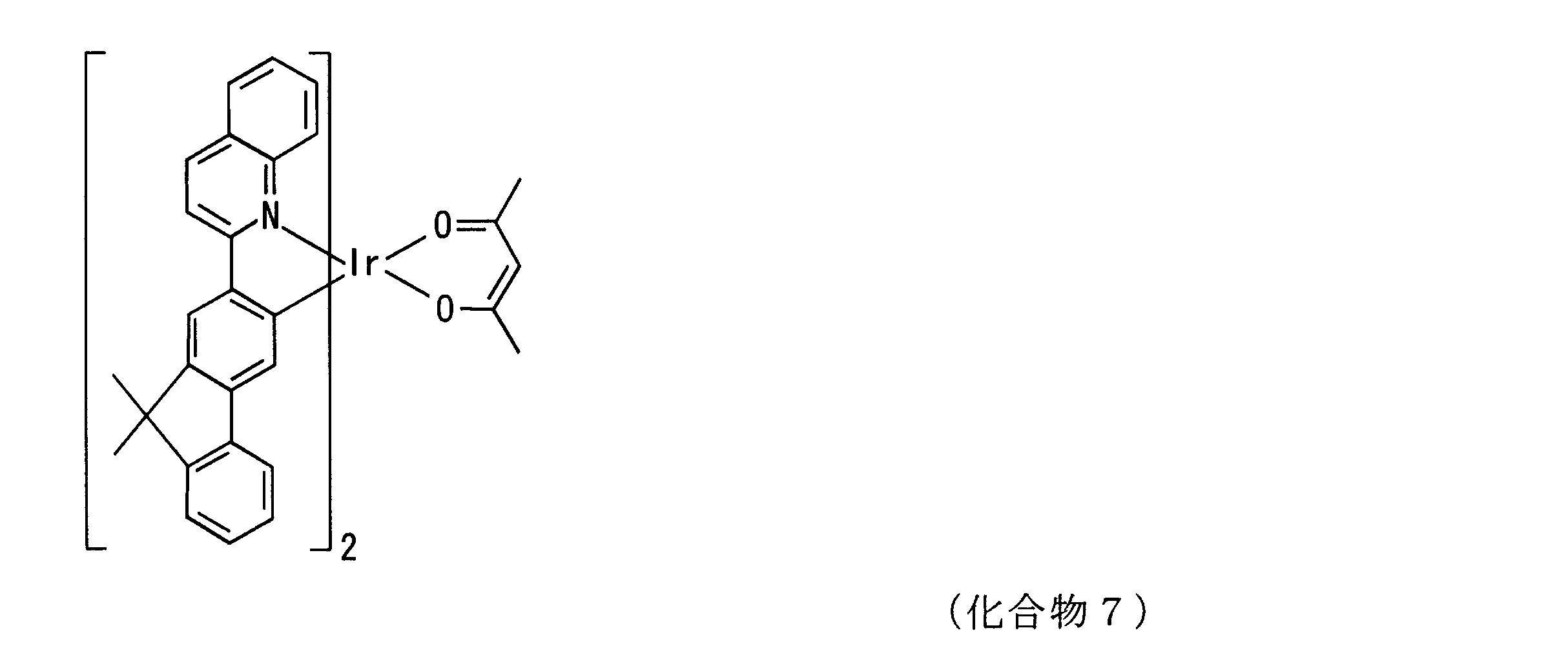
Hex-Ir(phq)2acac :
Bis [2-(4-n-hexylphenyl)quinoline)] (acetylacetonate)iridium(III)
Bis [2-(4-n-hexylphenyl)quinoline)] (acetylacetonate)iridium(III)
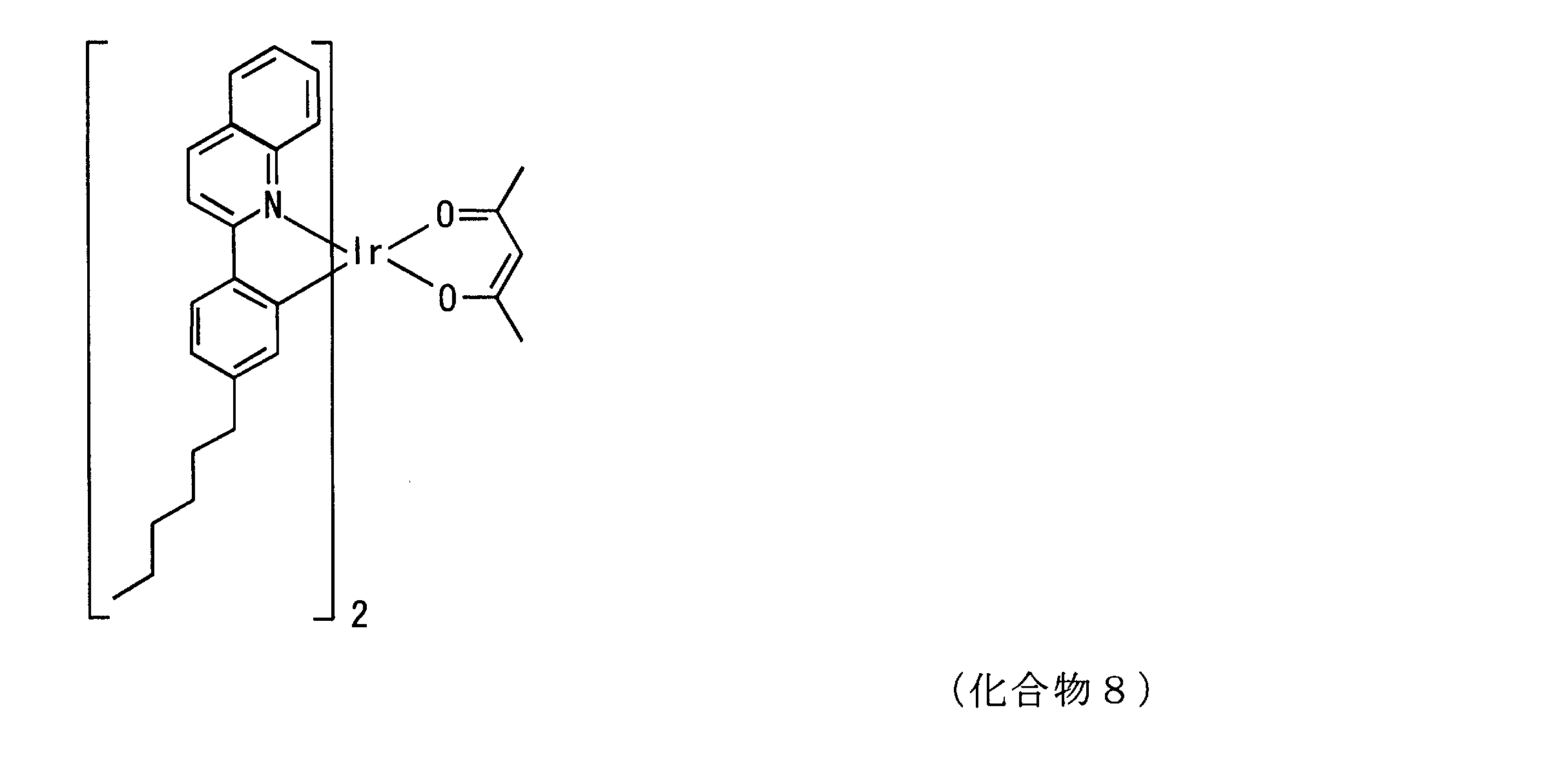
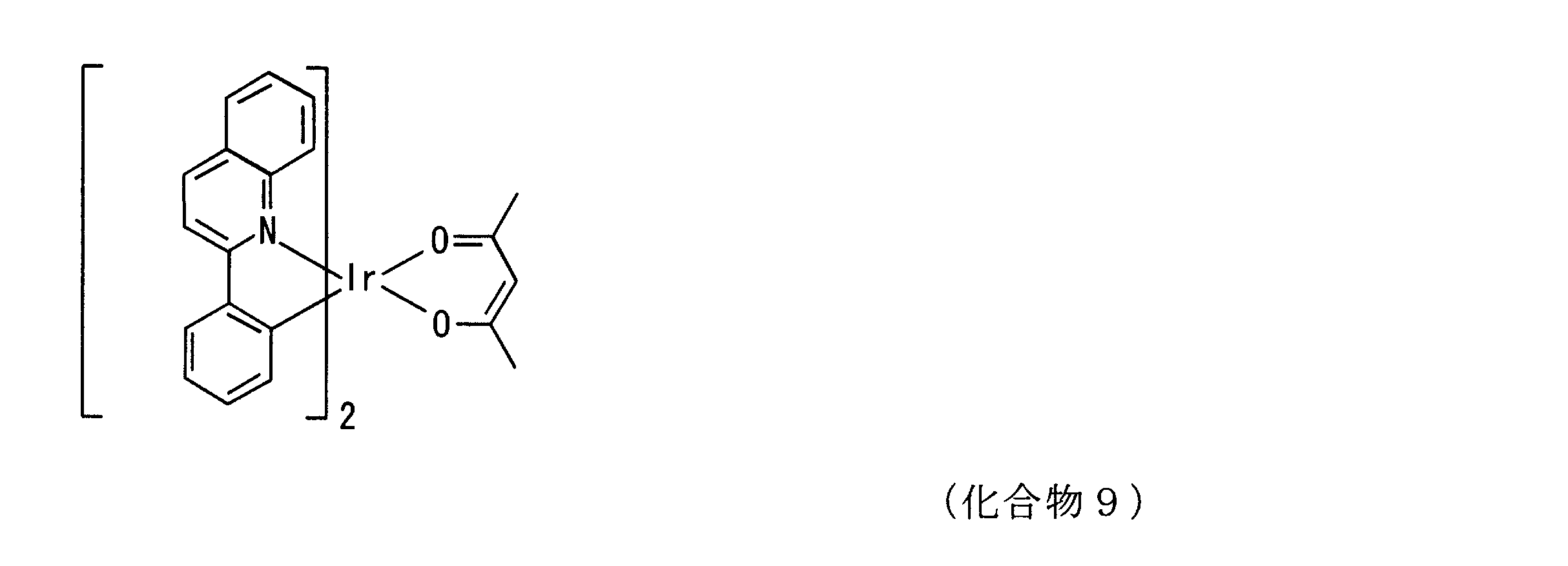
Ir(2-phq)2(acac) :
Bis(2-phenylquinoline)(acetylacetonate)iridium(III)
Bis(2-phenylquinoline)(acetylacetonate)iridium(III)
Ir(BT)2acac :
Bis(2-phenylbenzothiazolato)(acetylacetonate)iridium(III)
Bis(2-phenylbenzothiazolato)(acetylacetonate)iridium(III)

Ir(fbi)2(acac) :
Bis(2-(9,9-diethyl-9H-fluoren-2-yl)-1-phenyl-1H-benzimidazole) (acetylacetonate)iridium(III)
Bis(2-(9,9-diethyl-9H-fluoren-2-yl)-1-phenyl-1H-benzimidazole) (acetylacetonate)iridium(III)

Ir(ppy)2Pc :
Bis(2-phenylpyridine)(3-(pyridin-2-yl)-2H-chromen-2-onate)iridium(III)
Bis(2-phenylpyridine)(3-(pyridin-2-yl)-2H-chromen-2-onate)iridium(III)

PQ2Ir(dpm) :
Bis(2-phenylquinoline)(2,2,6,6-tetramethylheptane-3,5-dionate)iridium(III)
Bis(2-phenylquinoline)(2,2,6,6-tetramethylheptane-3,5-dionate)iridium(III)

Bis(phenylisoquinoline)(2,2,6,6-tetramethylheptane-3,5-dionate)iridium(III)

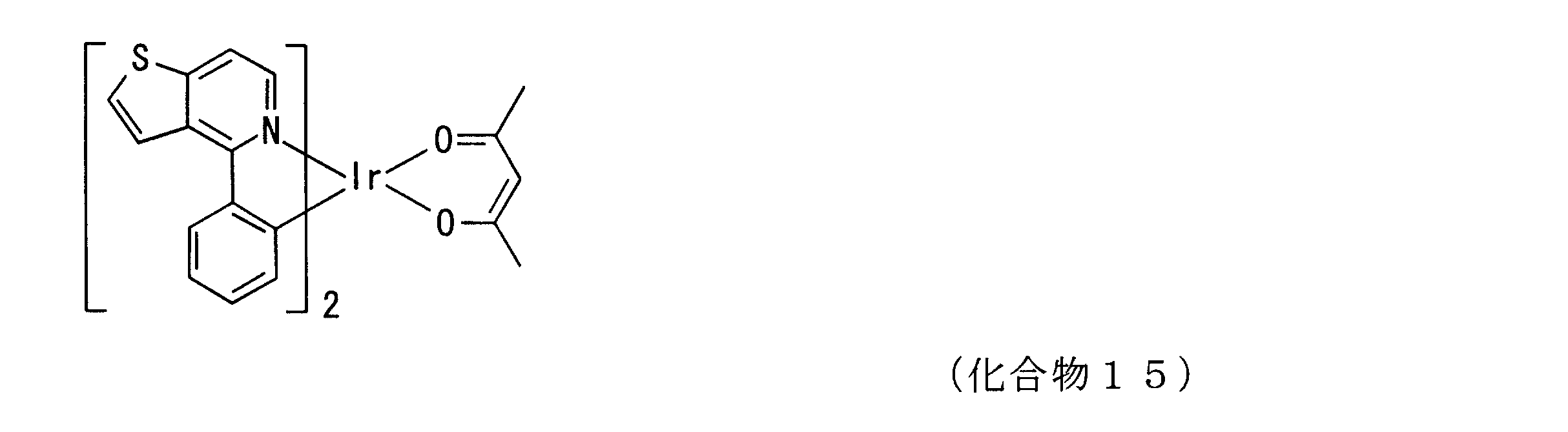
PO-01 :
Bis(4-phenylthieno[3,2-c]pyridinato-N,C2')acetylacetonate iridium(III)
Bis(4-phenylthieno[3,2-c]pyridinato-N,C2')acetylacetonate iridium(III)
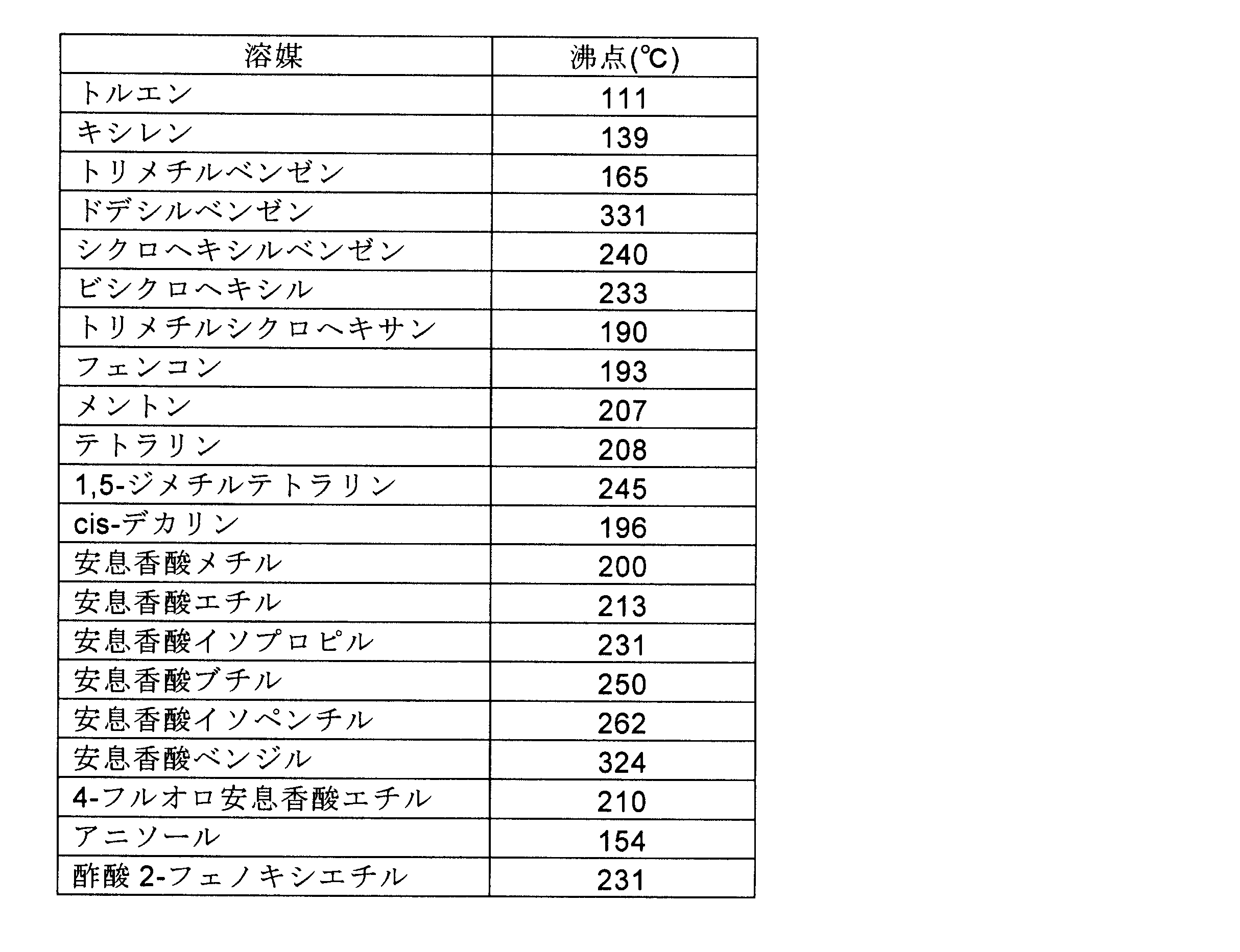
[溶媒](国内各社製)
--実験--
サンプル管に化合物1乃至化合物15の粉末をそれぞれ3mg~5mgの入れ、表1に記載の溶媒を1g相当を当該サンプル管にそれぞれ入れ、その後、粉末と溶媒が撹拌、混合された塗布液体(インク)を作製した。
サンプル管に化合物1乃至化合物15の粉末をそれぞれ3mg~5mgの入れ、表1に記載の溶媒を1g相当を当該サンプル管にそれぞれ入れ、その後、粉末と溶媒が撹拌、混合された塗布液体(インク)を作製した。
作製した塗布液体を200℃~230℃に加熱されたホットプレートにて10分~60分保持しそれぞれ観察した。その後、365nmのハンディUVランプにて発光の有無をそれぞれ確認した。
表2は発光実験の結果を溶媒の沸点値及び極性要因とともに示す。発光の有は○で無は×で示す。

以上の判定結果から、主に炭化水素の溶媒の炭素骨格において第3級炭素原子のある溶媒、すなわち第3級炭素原子にH基が一つで結合している溶媒を用いた場合、非プロトン性溶媒であっても発光が消光することが分った。また、非プロトン性溶媒のうちハロゲン基がある溶媒も同様に消光していることが分った。このことは、溶媒骨格にてH基が一つで存在する場合、電荷バランス不安定であるため加熱によりH基が解離し易く、乖離したH+が補助配位子に吸着し電荷バランスを崩し、そして金属錯体がラジカル状態、或いは分解するため発光が消光すると推察される。ここで、アプロチック溶媒は炭素骨格の第3級炭素原子に水素基が1つのみ結合した構造が存在しない分子構造を有し、加熱条件下に解離してプロトン(H+)を生じない溶媒を意味する。金属錯体組成物の溶媒として、ドデシルベンゼン、テトラリン、1,5-ジメチルテトラリン、安息香酸メチル、安息香酸エチル、安息香酸イソプロピル、安息香酸ブチル、安息香酸ベンジル、酢酸2-フェノキシエチル、及びジフェニルエーテルのアプロチック溶媒が好適であった。
--実施例:(素子の性能評価)--
以下に示す複数の有機EL素子を作製し、発光特性を測定、評価した。
以下に示す複数の有機EL素子を作製し、発光特性を測定、評価した。
化合物9のIr(2-phq)2(acac)を、それぞれ上記試験で好適であったドデシルベンゼン、テトラリン、1,5-ジメチルテトラリン、安息香酸メチル、安息香酸エチル、安息香酸イソプロピル、安息香酸ブチル、安息香酸ベンジル、酢酸2-フェノキシエチル、及びジフェニルエーテルに溶解して、有機電界発光素子用金属錯体組成物(インク)を調製した。固型分の発光ドーパントであるIr(2-phq)2(acac)とホスト材料である2,6?ビス(3?9H?カルバゾール?9?イル?フェニル)ピリジン(2,6-bis(3-9-H-carbazol-9-yl-phenyl)pyridine:(26DCzPPy))の濃度はそれぞれ6wt%であった。
陽極として透明電極ITOを形成したガラス基板上に、真空蒸着により順に、正孔注入・輸送層としてPEDOT:PSS(ポリ(3,4-エチレンジオキシチオフェン):ポリ(スチレンスルホネート)poly(3, 4-ethylenedioxythiophene):poly(styrenesulfonate))を32nmの厚さで形成した。
かかる正孔注入・輸送層上に上記インクによるインクジェット塗布を行い、乾燥させて、発光層を38nmの厚さで形成した。発光層の上に、真空蒸着により順に、電子輸送層としてAlq3(tris(8-hydroxy-quinolinato)aluminum)を60nmの厚さで形成し、その上に、電子注入層Li2O(1nm厚)及び陰極Al(80nm厚)を形成した。200℃以上の下でのインクジェット法を用いて有機材料層を塗り分ける際、射出ヘッドの当該金属錯体組成物の目詰まりの不具合は生じなかった。
素子の積層構成は陽極/正孔注入・輸送層/発光層/電子輸送層/電子注入層/陰極の順で、ITO/PEDOT:PSS/Ir(2-phq)2(acac):26DCzPPy/Alq3/Li2O/Alであった。200℃の加熱にもかかわらず何れの素子も赤色の発光を確認できた。
以上、本発明の実施例を有機EL素子により説明したが、本発明はこれら実施例に限定されるものではない。
1 基板
2 陽極
3 正孔注入層
4 正孔輸送層
5 発光層
6 正孔阻止層
7 電子輸送層
8 電子注入層
9 陰極
2 陽極
3 正孔注入層
4 正孔輸送層
5 発光層
6 正孔阻止層
7 電子輸送層
8 電子注入層
9 陰極
Claims (8)
- 中心金属、有機配位子及び補助配位子を有する発光性有機金属錯体とアプロチック溶媒とを含有することを特徴とする有機電界発光素子用金属錯体組成物。
- 前記アプロチック溶媒は炭素骨格の第3級炭素原子に水素基が1つのみ結合した構造が存在しない分子構造を有する非プロトン性極性溶媒の群から選択されることを特徴とする請求項1に記載の有機電界発光素子用金属錯体組成物。
- 前記アプロチック溶媒はハロゲン基が含有されてない分子構造を有する非プロトン性極性溶媒の群から選択されることを特徴とする請求項1又は2に記載の有機電界発光素子用金属錯体組成物。
- 前記アプロチック溶媒は沸点が200℃以上である非プロトン性極性溶媒の群から選択されることを特徴とする請求項1乃至3のいずれか1に記載の有機電界発光素子用金属錯体組成物。
- 前記アプロチック溶媒はドデシルベンゼン、テトラリン、1,5-ジメチルテトラリン、安息香酸メチル、安息香酸エチル、安息香酸イソプロピル、安息香酸ブチル、安息香酸ベンジル、酢酸2-フェノキシエチル、ジフェニルエーテル、ドデシルベンゼン及びそれらの組合せから成る群から選択されることを特徴とする請求項4に記載の有機電界発光素子用金属錯体組成物。
- 前記補助配位子は下記(1)式の二座配位子のアセチルアセテート、下記(2)式の二座配位子のカーボキシピリジル、下記(3)式の二座配位子のピラゾール-ボロネート、下記(4)式の二座配位子のピラジン-テトラゾロネート、下記(5)式の二座配位子のピリジンクロメンネート、下記(6)式の二座配位子のテトラメチルへプタンジネートのいずれか1つの骨格を有することを特徴とする請求項1乃至5のいずれか1に記載の有機電界発光素子用金属錯体組成物。



- 対向する1対の陽極及び陰極の間に積層配置されかつ発光層を含む複数の有機材料層を備えた有機電界発光素子であって、
前記有機材料層の少なくとも1層は、前記請求項1乃至6のいずれか1に記載の前記有機金属錯体組成物が湿式塗布され乾燥して形成された層であることを特徴とする有機電界発光素子。 - 前記有機金属錯体組成物を用いて形成された層が、発光層であることを特徴とする請求項7に記載の有機電界発光素子。
Priority Applications (1)
| Application Number | Priority Date | Filing Date | Title |
|---|---|---|---|
| PCT/JP2011/060475 WO2012147208A1 (ja) | 2011-04-28 | 2011-04-28 | 有機電界発光素子用金属錯体組成物 |
Applications Claiming Priority (1)
| Application Number | Priority Date | Filing Date | Title |
|---|---|---|---|
| PCT/JP2011/060475 WO2012147208A1 (ja) | 2011-04-28 | 2011-04-28 | 有機電界発光素子用金属錯体組成物 |
Publications (1)
| Publication Number | Publication Date |
|---|---|
| WO2012147208A1 true WO2012147208A1 (ja) | 2012-11-01 |
Family
ID=47071748
Family Applications (1)
| Application Number | Title | Priority Date | Filing Date |
|---|---|---|---|
| PCT/JP2011/060475 Ceased WO2012147208A1 (ja) | 2011-04-28 | 2011-04-28 | 有機電界発光素子用金属錯体組成物 |
Country Status (1)
| Country | Link |
|---|---|
| WO (1) | WO2012147208A1 (ja) |
Cited By (9)
| Publication number | Priority date | Publication date | Assignee | Title |
|---|---|---|---|---|
| CN104178117A (zh) * | 2013-05-22 | 2014-12-03 | 海洋王照明科技股份有限公司 | 一种蓝光有机电致发光材料及其制备方法和应用 |
| CN104177437A (zh) * | 2013-05-22 | 2014-12-03 | 海洋王照明科技股份有限公司 | 蓝色磷光材料铱金属配合物、其制备方法及有机电致发光器件 |
| CN104178109A (zh) * | 2013-05-22 | 2014-12-03 | 海洋王照明科技股份有限公司 | 一种蓝光有机电致发光材料及其制备方法和应用 |
| CN104178111A (zh) * | 2013-05-22 | 2014-12-03 | 海洋王照明科技股份有限公司 | 一种蓝光有机电致发光材料及其制备方法和应用 |
| CN104178107A (zh) * | 2013-05-22 | 2014-12-03 | 海洋王照明科技股份有限公司 | 蓝色磷光铱金属配合物、其制备方法及有机电致发光器件 |
| JP2014534606A (ja) * | 2011-08-26 | 2014-12-18 | メルク パテント ゲゼルシャフト ミット ベシュレンクテル ハフツングMerck Patent Gesellschaft mit beschraenkter Haftung | 有機半導体配合物 |
| WO2016021784A1 (ko) * | 2014-08-08 | 2016-02-11 | 서울대학교 산학협력단 | 유기 발광 소자 |
| JP2018009078A (ja) * | 2016-07-12 | 2018-01-18 | 三星電子株式会社Samsung Electronics Co.,Ltd. | 有機発光素子用インキ組成物、並びにこれを用いた有機発光素子およびその製造方法 |
| CN109312183A (zh) * | 2016-06-17 | 2019-02-05 | 默克专利有限公司 | 有机功能材料的制剂 |
Citations (10)
| Publication number | Priority date | Publication date | Assignee | Title |
|---|---|---|---|---|
| JP2003084697A (ja) * | 2001-09-10 | 2003-03-19 | Brother Ind Ltd | 表示体、表示体の製造方法、及び表示体の製造装置 |
| JP2003238286A (ja) * | 2001-10-10 | 2003-08-27 | Seiko Epson Corp | 薄膜の形成方法、この方法に用いる溶液、電子デバイスの形成方法 |
| WO2006100888A1 (ja) * | 2005-03-22 | 2006-09-28 | Konica Minolta Holdings, Inc. | 有機el素子用材料、有機el素子、表示装置及び照明装置 |
| JP2007522126A (ja) * | 2004-01-26 | 2007-08-09 | ユニバーサル ディスプレイ コーポレーション | 改善された電界発光安定性 |
| JP2007208217A (ja) * | 2006-02-06 | 2007-08-16 | Fujifilm Corp | 有機電界発光素子 |
| JP2008019443A (ja) * | 2001-03-27 | 2008-01-31 | Sumitomo Chemical Co Ltd | 高分子発光体およびそれを用いた高分子発光素子 |
| JP2009500360A (ja) * | 2005-07-08 | 2009-01-08 | メルク パテント ゲーエムベーハー | 金属錯体 |
| JP2009059846A (ja) * | 2007-08-31 | 2009-03-19 | Mitsubishi Chemicals Corp | 有機電界発光素子用組成物、有機電界発光素子および有機電界発光素子の製造方法 |
| JP2009140922A (ja) * | 2007-11-16 | 2009-06-25 | Sumitomo Chemical Co Ltd | スリット状吐出口から塗工液を吐出する塗布法用塗工液 |
| WO2009110360A1 (ja) * | 2008-03-05 | 2009-09-11 | 出光興産株式会社 | 高分子化合物及びそれを用いた有機エレクトロルミネッセンス素子 |
-
2011
- 2011-04-28 WO PCT/JP2011/060475 patent/WO2012147208A1/ja not_active Ceased
Patent Citations (10)
| Publication number | Priority date | Publication date | Assignee | Title |
|---|---|---|---|---|
| JP2008019443A (ja) * | 2001-03-27 | 2008-01-31 | Sumitomo Chemical Co Ltd | 高分子発光体およびそれを用いた高分子発光素子 |
| JP2003084697A (ja) * | 2001-09-10 | 2003-03-19 | Brother Ind Ltd | 表示体、表示体の製造方法、及び表示体の製造装置 |
| JP2003238286A (ja) * | 2001-10-10 | 2003-08-27 | Seiko Epson Corp | 薄膜の形成方法、この方法に用いる溶液、電子デバイスの形成方法 |
| JP2007522126A (ja) * | 2004-01-26 | 2007-08-09 | ユニバーサル ディスプレイ コーポレーション | 改善された電界発光安定性 |
| WO2006100888A1 (ja) * | 2005-03-22 | 2006-09-28 | Konica Minolta Holdings, Inc. | 有機el素子用材料、有機el素子、表示装置及び照明装置 |
| JP2009500360A (ja) * | 2005-07-08 | 2009-01-08 | メルク パテント ゲーエムベーハー | 金属錯体 |
| JP2007208217A (ja) * | 2006-02-06 | 2007-08-16 | Fujifilm Corp | 有機電界発光素子 |
| JP2009059846A (ja) * | 2007-08-31 | 2009-03-19 | Mitsubishi Chemicals Corp | 有機電界発光素子用組成物、有機電界発光素子および有機電界発光素子の製造方法 |
| JP2009140922A (ja) * | 2007-11-16 | 2009-06-25 | Sumitomo Chemical Co Ltd | スリット状吐出口から塗工液を吐出する塗布法用塗工液 |
| WO2009110360A1 (ja) * | 2008-03-05 | 2009-09-11 | 出光興産株式会社 | 高分子化合物及びそれを用いた有機エレクトロルミネッセンス素子 |
Cited By (12)
| Publication number | Priority date | Publication date | Assignee | Title |
|---|---|---|---|---|
| JP2014534606A (ja) * | 2011-08-26 | 2014-12-18 | メルク パテント ゲゼルシャフト ミット ベシュレンクテル ハフツングMerck Patent Gesellschaft mit beschraenkter Haftung | 有機半導体配合物 |
| US9805838B2 (en) | 2011-08-26 | 2017-10-31 | Merck Patent Gmbh | Organic semiconductor formulation |
| CN104178117A (zh) * | 2013-05-22 | 2014-12-03 | 海洋王照明科技股份有限公司 | 一种蓝光有机电致发光材料及其制备方法和应用 |
| CN104177437A (zh) * | 2013-05-22 | 2014-12-03 | 海洋王照明科技股份有限公司 | 蓝色磷光材料铱金属配合物、其制备方法及有机电致发光器件 |
| CN104178109A (zh) * | 2013-05-22 | 2014-12-03 | 海洋王照明科技股份有限公司 | 一种蓝光有机电致发光材料及其制备方法和应用 |
| CN104178111A (zh) * | 2013-05-22 | 2014-12-03 | 海洋王照明科技股份有限公司 | 一种蓝光有机电致发光材料及其制备方法和应用 |
| CN104178107A (zh) * | 2013-05-22 | 2014-12-03 | 海洋王照明科技股份有限公司 | 蓝色磷光铱金属配合物、其制备方法及有机电致发光器件 |
| WO2016021784A1 (ko) * | 2014-08-08 | 2016-02-11 | 서울대학교 산학협력단 | 유기 발광 소자 |
| CN109312183A (zh) * | 2016-06-17 | 2019-02-05 | 默克专利有限公司 | 有机功能材料的制剂 |
| JP2019523998A (ja) * | 2016-06-17 | 2019-08-29 | メルク パテント ゲーエムベーハー | 有機機能材料の調合物 |
| JP2018009078A (ja) * | 2016-07-12 | 2018-01-18 | 三星電子株式会社Samsung Electronics Co.,Ltd. | 有機発光素子用インキ組成物、並びにこれを用いた有機発光素子およびその製造方法 |
| US11322695B2 (en) | 2016-07-12 | 2022-05-03 | Samsung Electronics Co., Ltd. | Ink composition for organic light-emitting device, organic light-emitting device including film formed by using the ink composition, and method of manufacturing the organic light-emitting device |
Similar Documents
| Publication | Publication Date | Title |
|---|---|---|
| KR101688317B1 (ko) | 저전압 구동 유기발광소자 및 이의 제조 방법 | |
| WO2012147208A1 (ja) | 有機電界発光素子用金属錯体組成物 | |
| JP5205584B2 (ja) | 有機電界発光素子および表示装置 | |
| KR101756498B1 (ko) | 부가 화합물을 함유하는 가교 전하 운반 층 | |
| US9166184B2 (en) | Organic light emitting device having three successive light emitting sub-layers with mixture matrix material for the second light emitting sub-layer and method of preparing same and display device thereof | |
| JP4789209B2 (ja) | 正孔輸送領域内の金属副層 | |
| CN102651454B (zh) | 一种电致发光器件、显示装置和电致发光器件制备方法 | |
| Lin et al. | A bipolar host containing carbazole/dibenzothiophene for efficient solution-processed blue and white phosphorescent OLEDs | |
| JP2007507107A (ja) | 非正孔阻止バッファ層を有するoled | |
| JP6153703B2 (ja) | 有機発光デバイス用の複合有機/無機層 | |
| CN1711652A (zh) | 有机器件结构及其制造方法 | |
| WO2011010696A1 (ja) | 有機エレクトロルミネッセント素子 | |
| US20120049164A1 (en) | Cross-Linked Hole Transport Layer With Hole Transport Additive | |
| KR100721551B1 (ko) | 백색 발광 유기전계발광소자 및 그를 구비하는유기전계발광표시장치 | |
| CN106531897B (zh) | 一种基于激基复合物的有机电致发光器件及其制备方法 | |
| CN101916830B (zh) | 白色有机电致发光器件及其制备方法 | |
| JP2013507013A (ja) | 低電圧エレクトロルミネッセンス装置用有機素子 | |
| Baek et al. | Optimization of white organic light emitting diodes based on emitting layer charge carrier conduction properties | |
| US8564015B2 (en) | Organic light-emitting diode with high color rendering | |
| CN103928627B (zh) | 一种修饰氧化铟锡阳极的制备方法 | |
| JP2013222615A (ja) | 有機エレクトロルミネッセンス素子の製造方法 | |
| WO2012169069A1 (ja) | 有機エレクトロルミネッセンスパネル | |
| CN105679963B (zh) | 一种有机电致发光器件 | |
| Lee et al. | Effect of stepwise doping on lifetime and efficiency of blue and white phosphorescent organic light emitting diodes | |
| Kim et al. | Electrical and Optical Properties of Phosphorescent Organic Light-Emitting Devices with a TAPC Host |
Legal Events
| Date | Code | Title | Description |
|---|---|---|---|
| 121 | Ep: the epo has been informed by wipo that ep was designated in this application |
Ref document number: 11864283 Country of ref document: EP Kind code of ref document: A1 |
|
| NENP | Non-entry into the national phase |
Ref country code: DE |
|
| 122 | Ep: pct application non-entry in european phase |
Ref document number: 11864283 Country of ref document: EP Kind code of ref document: A1 |
|
| NENP | Non-entry into the national phase |
Ref country code: JP |