WO2012144449A1 - バックライトユニット及び表示装置 - Google Patents
バックライトユニット及び表示装置 Download PDFInfo
- Publication number
- WO2012144449A1 WO2012144449A1 PCT/JP2012/060238 JP2012060238W WO2012144449A1 WO 2012144449 A1 WO2012144449 A1 WO 2012144449A1 JP 2012060238 W JP2012060238 W JP 2012060238W WO 2012144449 A1 WO2012144449 A1 WO 2012144449A1
- Authority
- WO
- WIPO (PCT)
- Prior art keywords
- light
- light guide
- light source
- guide plate
- backlight unit
- Prior art date
Links
Images


Classifications
-
- G—PHYSICS
- G02—OPTICS
- G02B—OPTICAL ELEMENTS, SYSTEMS OR APPARATUS
- G02B6/00—Light guides; Structural details of arrangements comprising light guides and other optical elements, e.g. couplings
- G02B6/0001—Light guides; Structural details of arrangements comprising light guides and other optical elements, e.g. couplings specially adapted for lighting devices or systems
- G02B6/0011—Light guides; Structural details of arrangements comprising light guides and other optical elements, e.g. couplings specially adapted for lighting devices or systems the light guides being planar or of plate-like form
- G02B6/0081—Mechanical or electrical aspects of the light guide and light source in the lighting device peculiar to the adaptation to planar light guides, e.g. concerning packaging
- G02B6/0086—Positioning aspects
- G02B6/0091—Positioning aspects of the light source relative to the light guide
-
- G—PHYSICS
- G02—OPTICS
- G02B—OPTICAL ELEMENTS, SYSTEMS OR APPARATUS
- G02B6/00—Light guides; Structural details of arrangements comprising light guides and other optical elements, e.g. couplings
- G02B6/0001—Light guides; Structural details of arrangements comprising light guides and other optical elements, e.g. couplings specially adapted for lighting devices or systems
- G02B6/0011—Light guides; Structural details of arrangements comprising light guides and other optical elements, e.g. couplings specially adapted for lighting devices or systems the light guides being planar or of plate-like form
- G02B6/0033—Means for improving the coupling-out of light from the light guide
- G02B6/005—Means for improving the coupling-out of light from the light guide provided by one optical element, or plurality thereof, placed on the light output side of the light guide
- G02B6/0053—Prismatic sheet or layer; Brightness enhancement element, sheet or layer
-
- G—PHYSICS
- G02—OPTICS
- G02B—OPTICAL ELEMENTS, SYSTEMS OR APPARATUS
- G02B6/00—Light guides; Structural details of arrangements comprising light guides and other optical elements, e.g. couplings
- G02B6/0001—Light guides; Structural details of arrangements comprising light guides and other optical elements, e.g. couplings specially adapted for lighting devices or systems
- G02B6/0011—Light guides; Structural details of arrangements comprising light guides and other optical elements, e.g. couplings specially adapted for lighting devices or systems the light guides being planar or of plate-like form
- G02B6/0075—Arrangements of multiple light guides
- G02B6/0076—Stacked arrangements of multiple light guides of the same or different cross-sectional area
-
- G—PHYSICS
- G09—EDUCATION; CRYPTOGRAPHY; DISPLAY; ADVERTISING; SEALS
- G09G—ARRANGEMENTS OR CIRCUITS FOR CONTROL OF INDICATING DEVICES USING STATIC MEANS TO PRESENT VARIABLE INFORMATION
- G09G5/00—Control arrangements or circuits for visual indicators common to cathode-ray tube indicators and other visual indicators
- G09G5/10—Intensity circuits
-
- G—PHYSICS
- G02—OPTICS
- G02B—OPTICAL ELEMENTS, SYSTEMS OR APPARATUS
- G02B6/00—Light guides; Structural details of arrangements comprising light guides and other optical elements, e.g. couplings
- G02B6/0001—Light guides; Structural details of arrangements comprising light guides and other optical elements, e.g. couplings specially adapted for lighting devices or systems
- G02B6/0011—Light guides; Structural details of arrangements comprising light guides and other optical elements, e.g. couplings specially adapted for lighting devices or systems the light guides being planar or of plate-like form
- G02B6/0033—Means for improving the coupling-out of light from the light guide
- G02B6/0035—Means for improving the coupling-out of light from the light guide provided on the surface of the light guide or in the bulk of it
- G02B6/0036—2-D arrangement of prisms, protrusions, indentations or roughened surfaces
-
- G—PHYSICS
- G02—OPTICS
- G02B—OPTICAL ELEMENTS, SYSTEMS OR APPARATUS
- G02B6/00—Light guides; Structural details of arrangements comprising light guides and other optical elements, e.g. couplings
- G02B6/0001—Light guides; Structural details of arrangements comprising light guides and other optical elements, e.g. couplings specially adapted for lighting devices or systems
- G02B6/0011—Light guides; Structural details of arrangements comprising light guides and other optical elements, e.g. couplings specially adapted for lighting devices or systems the light guides being planar or of plate-like form
- G02B6/0033—Means for improving the coupling-out of light from the light guide
- G02B6/0058—Means for improving the coupling-out of light from the light guide varying in density, size, shape or depth along the light guide
- G02B6/0061—Means for improving the coupling-out of light from the light guide varying in density, size, shape or depth along the light guide to provide homogeneous light output intensity
-
- G—PHYSICS
- G02—OPTICS
- G02F—OPTICAL DEVICES OR ARRANGEMENTS FOR THE CONTROL OF LIGHT BY MODIFICATION OF THE OPTICAL PROPERTIES OF THE MEDIA OF THE ELEMENTS INVOLVED THEREIN; NON-LINEAR OPTICS; FREQUENCY-CHANGING OF LIGHT; OPTICAL LOGIC ELEMENTS; OPTICAL ANALOGUE/DIGITAL CONVERTERS
- G02F1/00—Devices or arrangements for the control of the intensity, colour, phase, polarisation or direction of light arriving from an independent light source, e.g. switching, gating or modulating; Non-linear optics
- G02F1/01—Devices or arrangements for the control of the intensity, colour, phase, polarisation or direction of light arriving from an independent light source, e.g. switching, gating or modulating; Non-linear optics for the control of the intensity, phase, polarisation or colour
- G02F1/13—Devices or arrangements for the control of the intensity, colour, phase, polarisation or direction of light arriving from an independent light source, e.g. switching, gating or modulating; Non-linear optics for the control of the intensity, phase, polarisation or colour based on liquid crystals, e.g. single liquid crystal display cells
- G02F1/133—Constructional arrangements; Operation of liquid crystal cells; Circuit arrangements
- G02F1/1333—Constructional arrangements; Manufacturing methods
- G02F1/1335—Structural association of cells with optical devices, e.g. polarisers or reflectors
- G02F1/1336—Illuminating devices
- G02F1/133615—Edge-illuminating devices, i.e. illuminating from the side
Definitions
- the present invention relates to a backlight unit and a display device.
- DV display dual view display
- a DV display can display two different images at the same time, each image being only viewable from a particular direction.
- the emitted light emitted from the DV display has luminance directivity in a direction in which each image can be viewed.
- the luminance directivity of the light emitted from the liquid crystal panel largely depends on the luminance directivity of the backlight light emitted from the backlight.
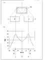
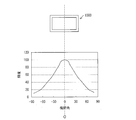
- the backlight has luminance directivity in the front direction of the display 1000 (viewing angle 0 ° in FIG. 14).
- the dual view display (hereinafter referred to as “DV display”) displayed on the DV display is centered on the display in the direction of the viewing angle of ⁇ 45 °.
- the backlight unit having the luminance directivity in the direction of the viewing angle of 0 ° shown in FIG. 14 is used for DV display, the luminance of the backlight light is reduced by about 60% around the viewing angle of ⁇ 45 °. As a result, the display quality deteriorates. Further, in order to increase the luminance in the vicinity of the viewing angle ⁇ 45 degrees, it is necessary to increase the luminance of the backlight as a whole, and there is a problem that the power consumption of the backlight is unnecessarily increased.
- Patent Document 1 discloses a backlight unit for a DV display (hereinafter simply referred to as “DV backlight unit”).
- FIG. 14 is a perspective view showing a configuration of a conventional DV backlight unit.
- the DV backlight units are arranged in order from the front side to the back side.
- a sheet 1015, a prism sheet 1014, a diffusion sheet 1013, a light guide plate 1012, and a reflection plate 1016 are provided. Further, a plurality of light sources 1011 are arranged along one side of the four sides of the light guide plate 1012.
- the prism forming surface of the prism sheet 1014 faces the side where the light guide plate 1012 is disposed, and its prism axis (prism ridgeline) is arranged in parallel along the vertical direction of the liquid crystal screen.
- the prism forming surface of the prism sheet 1015 faces the liquid crystal panel, and the prism axis is arranged so as to coincide with the horizontal direction of the liquid crystal screen.
- the light emitted from the light source 1011 enters the light guide plate 1012 from one side surface of the light guide plate 1012, and the incident light exits in a planar shape from one surface of the light guide plate 1012.
- Light emitted from the light guide plate 1012 is converted into light having luminance directivity in two directions by two prism sheets 1014 and 1015 that are incident through the diffusion sheet 1013, and is incident on a liquid crystal panel capable of DV display. To do.
- a backlight unit having a common configuration is preferable regardless of whether it is a small size, a medium size, or a large size, in order to simplify the design and reduce the cost for maintaining the manufacturing equipment.
- the light source 1011 is arranged along one side of one light guide plate 1012.
- the DV backlight unit shown in FIG. 14 when the DV backlight unit shown in FIG. 14 is enlarged, the color of the light in the vicinity of the light source 1012 and the light in the vicinity of the side surface away from the light source 1012 out of the light emitted in a planar shape from the light guide plate 1012. Therefore, the display quality is deteriorated.
- the present invention has been made in view of the above problems, and its object is to emit light having luminance directivity in a plurality of different directions without deterioration of display quality even when the size is increased. is there.
- the backlight unit of the present invention is a backlight unit having a light source and a light guide member, and the light source and the light guide member include the first and second light sources, 1 and a second light guide member, wherein the first light source is disposed on a side surface of the first light guide member, and the second light source is disposed on a side surface of the second light guide member.
- the first and second light sources are arranged to face each other via the first and second light guide members in a plan view, and further, the first or second light guide member is disposed.
- An optical path changing member for changing the optical path of the light passing therethrough which has an incident surface that directly emits light emitted from the light source and an output surface that directly emits incident light from the incident surface toward an external display panel It is characterized by having.
- the first and second light sources arranged to face each other via the first and second light guide members, and the first light source arranged on the side surface are the first.
- first and second light sources opposed to each other through the first and second light guide members are provided in a plan view, even if the size is increased, the distance between both side surfaces opposed in the plan view Can be prevented from changing, and display quality can be prevented from deteriorating.
- the backlight unit of the present invention is a backlight unit having a light source and a light guide member, and the light source and the light guide member include first and second light sources, and first and second light guide members, respectively.
- the first light source is disposed on a side surface of the first light guide member
- the second light source is disposed on a side surface of the second light guide member.
- the two light sources are arranged so as to face each other via the first and second light guide members in plan view, and further, are incident surfaces on which light emitted from the first or second light guide member is directly incident.
- an exit surface that directly emits incident light from the entrance surface toward an external display panel, and includes an optical path changing member that changes the optical path of the passing light.
- the display quality is not deteriorated even when the size is increased, and it is possible to emit light having luminance directivity in a plurality of different directions.
- FIG. 1 is a diagram illustrating an overall configuration of a display system according to an embodiment of the present invention.
- the state of DV display of the display system and the state of luminance of the displayed image are shown.
- FIGS. 1 to 12 An embodiment of the present invention will be described with reference to FIGS. 1 to 12 as follows. Descriptions of configurations other than those described in the following specific items may be omitted as necessary. However, in the case where they are described in other items, the configurations are the same. For convenience of explanation, members having the same functions as those shown in each item are given the same reference numerals, and the explanation thereof is omitted as appropriate.
- FIG. 1 is a diagram showing the overall configuration of the display system 100.
- a display system 100 has a liquid crystal panel (display panel) 5 having an image display area, a BL (backlight) unit 20 that illuminates the liquid crystal panel 5 from the back side, and an image display area.
- the frame 9 enclosing the liquid crystal panel 5 and the BL unit 20 and sensors (luminance sensors) 6A and 6B for detecting the amount of light emitted from the liquid crystal panel 5 are provided.
- the display system 100 includes a calculation unit 7, a light source drive control unit 8, and a memory 10 for controlling the light amounts of the light sources 4A and 4B in accordance with outputs from the sensors 6A and 6B.
- the BL unit 20 includes an optical path changing member 1 serving as an emission surface of the BL unit 20, a light guide plate (first light guide member) 2A, a light guide plate (second light guide member) 2B, and a reflection plate (reflection member). 3 and a light source (first light source) 4A and a light source (second light source) 4B. As will be described later, the BL unit 20 has luminance directivities in two different directions.
- the display system 100 is a display system capable of simultaneously displaying two or more images in different directions.
- the display system 100 can perform dual view display (hereinafter referred to as DV display) that displays two images simultaneously, or quartet view display (hereinafter referred to as CV display) that displays four images simultaneously. .
- DV display dual view display
- CV display quartet view display
- the display system 100 will be described as a display system that can mainly perform DV display.
- FIG. 2 shows a DV display state of the display system 100 and a luminance state of the displayed image.
- the display system 100 includes a right image IR that can be viewed when viewing the display system 100 from the right side and a left image IL that can be viewed when viewing the display system 100 from the left side. Both can be displayed simultaneously.
- the right image IR side (the right side of the drawing) may be referred to as “A side”
- the left image IL side (the left side of the drawing) may be referred to as “B side”.
- the light emitted from the display system 100 has a viewing angle of ⁇ 45 degrees and a brightness peaking at a peak angle while suppressing the brightness in the frontal direction (viewing angle direction 0 degree). It is comprised so that it may become.
- the viewing angle when viewing the display system 100 from the front is set to 0 degree
- the viewing angle from 0 degree to the A side is set to +
- the viewing angle from 0 degree to the B side viewing angle Is expressed as-.
- the right image IR which is an image with good display quality
- the left image IL can be viewed by the user on the B side.
- the display system 100 is not limited to DV display or CV display, and may be capable of 3D (stereoscopic) display.
- 3D stereo-dispelectron emission display
- the display system 100 for DV display by adjusting the relationship between the parallax barrier and the pixel structure from the display system 100 for DV display, a display system capable of 3D display for the naked eye without using 3D glasses can be obtained.
- the display system 100 will be described mainly as a display system capable of DV display.
- each component of the display system 100 will be described in order.
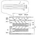
- FIG. 3 is a cross-sectional view showing the configuration of the liquid crystal panel 5 and the BL unit 20.
- the BL (backlight) unit 20 includes an optical path changing member 1, a light guide plate (first light guide member) 2A, a light guide plate (second light guide member) 2B, and a reflection plate (reflection member). 3), a light source (first light source) 4A, and a light source (second light source) 4B.
- front in the present specification means the surface on the side where the liquid crystal panel 5 displays an image (that is, the side on which the user views the liquid crystal panel 5).
- rear surface in the present specification means a surface opposite to the side on which the liquid crystal panel 5 displays an image.
- the BL unit 20 includes a liquid crystal panel 5, an optical path changing member 1, a light guide plate 2B, a light guide plate 2A, and a reflection plate 3 in order from the front side to the back side.
- the light source 4A is disposed on the side surface of the light guide plate 2A, and the light source 4B is disposed on the side surface of the light guide plate 2B.
- the light source 4A is disposed on one side (side surface) of the light guide plate 2A, and the light source 4B is disposed on one side (side surface) of the light guide plate 2B.
- the light sources 4A and 4B are disposed to face each other via the light guide plates 2A and 2B when the BL unit 20 is viewed in plan.
- the light guide plate 2A may be disposed on the front side, and the light guide plate 2B may be disposed on the back side.
- the BL unit 20 has a light source 4A and a light source 4B opposed to each other through the light guide plates 2A and 2B, a light guide plate 2A in which the light source 4A is arranged on one side, and a light source 4B on the side. Are disposed, and an optical path changing member 1 that changes the optical path of light passing therethrough.
- emission light A and B light having luminance directivity in which the luminance distribution in at least two directions different from the normal direction of the display screen of the liquid crystal panel 5 is maximized.
- emission light A and B light having luminance directivity in which the luminance distribution in at least two directions different from the normal direction of the display screen of the liquid crystal panel 5 is maximized.
- emission light A and B light having luminance directivity in which the luminance distribution in at least two directions different from the normal direction of the display screen of the liquid crystal panel 5 is maximized.
- the light can be emitted from the SUF2.
- the sidelight-type backlight is one in which light source light is incident from the side surface of the light guide, the incident light is reflected inside, and is emitted in a planar shape from the exit surface of the light guide.
- Patent Document 1 when only one light guide that emits light incident from one end face of the light guide in a planar shape is used, the size of the light guide is increased (the area is increased). The color of will change.
- a configuration in which light sources are provided on both sides of one light guide plate can be considered as the configuration of the backlight unit so as to have luminance directivity in two directions.
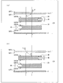
- FIG. 12 is a side view showing a state of the light guide plate in which the light sources 504A and 504B are arranged on the side surfaces facing each other.
- A) of FIG. 12 shows the state of the emitted light from the light guide plate in which the uneven pattern is sparse to dense from the right side to the left side of the paper, and (b) is the uneven pattern from dense to sparse from the central part to both side surfaces.
- C) shows the state of light emitted from a large light guide plate having a concavo-convex pattern from sparse to dense from the right side to the left side of the drawing.
- a light source 504A is disposed on one side surface of the opposite side surfaces of the light guide plate 502, and a light source 504B is disposed on the other side surface. ing.
- the concave / convex pattern is arranged from the side surface on the side where the light source 504B is arranged to the side surface on the side where the light source 504A is arranged so that the uneven pattern becomes dense. Has been.
- the uneven pattern is formed so that the in-plane luminance of the emitted light B emitted from the light source B is uniform.
- the light path through which the light emitted from the light sources 504A and 504B is guided in the light guide plate 502 is short.
- the light guide plate 502 even if the uneven pattern of the light guide plate 502 is aligned with the light source 504B (the light source 504B side is sparse and the light source 504A side is dense), the light emitted from the light source 504A Although it becomes weaker as it approaches the disposed side, it can reach the opposite side surface sufficiently and can be emitted as the emitted light A from the light emitting surface of the light guide plate 502.
- in-plane luminance variation is a problem.
- the concave / convex pattern of the light guide plate 502 is adjusted so that the central portion of the light guide plate 502 is dense and becomes sparse as it goes to both side surfaces. Then, the luminance variation in the surface of the emitted light A emitted from the light emitting surface of the light guide plate 502 from the light source 504A and the luminance variation in the surface of the emitted light B emitted from the light emitting surface of the light guide plate 502 from the light source 504B. Can be made equal.
- each of the outgoing light A and the outgoing light B can be adjusted by adjusting the concavo-convex pattern of the light guide plate even with a single light guide plate. In-plane luminance variation can be adjusted.
- the white light when the white light is repeatedly reflected a plurality of times in the light guide plate, the light amount on the low wavelength side gradually attenuates and the color changes. A smaller number of reflections is preferable.
- the light incident on the light guide plate 502 from the light sources 504A and 504B is sequentially emitted from the light exit surface as the exit light A and the exit light B, and is not reflected on the opposite side surface.
- the optical path length in the light guide plate 502 is short. For this reason, while uniforming the in-plane luminance variation of the emitted light A and B, all the light incident from the light sources 504A and 504B is emitted to the light emitting surface side of the light guide plate 502 up to the opposite side surface. I can't. For this reason, there is light reflected on a part of the opposite side surface.
- the optical path length inside the light guide plate 502 is short, so the light sources 504A and 504B enter the light guide plate 502.
- the number of reflections is small, and the change in the color of the light caused by reflection on the opposite side surfaces of the light sources 504A and 504B does not matter much. .
- the size of the light guide plate is small, even if the light guide plate 502 is a single light guide plate 502, by adjusting the concave / convex pattern, in-plane luminance variation can be suppressed, and there is no problem in color change. It is possible to emit a level of emitted light A and B.
- the optical path in the light guide plate 502 becomes long.
- the uneven pattern is sparsely and densely formed on the back surface of the large light guide plate 502 from the side surface on the side where the light source 504B is disposed to the side surface on the side where the light source 504A is disposed.
- the concave / convex pattern is formed so that the in-plane luminance of the emitted light B emitted from the light source 504B is uniform as in the light guide plate 502 of FIG.
- the optical path of the light guide plate 502 is short in the case of a small size, the outgoing light A has reached the side surface on which the light source 504B is arranged.
- the optical path of the light guide plate 502 is long, so A does not reach the side surface on which the light source 504B is disposed, and the emitted light A varies in luminance within the surface.
- the light is also reflected on the side surface opposite to the side surface on which each of the light sources 504A and 504B is disposed, and the emitted light Variations in the in-plane colors of A and outgoing light B increase.
- the BL unit 20 includes light sources 4A and 4B that are opposed to each other via the light guide plates 2A and 2B when viewed in plan. That is, since the light sources 4A and 4B are arranged on both side surfaces opposed to each other in plan view, the color between both side surfaces opposed to each other in plan view can be prevented from changing even when the size is increased (large area). Display quality can be prevented.
- the BL unit 20 includes two light guide plates 2A and 2B, and the uneven patterns of the light guide plates 2A and 2B can be individually adjusted. In-plane brightness variation and color variation can be suppressed.
- the BL unit 20 includes a plurality of light guide plates 2A and a light guide plate 2B. Therefore, by adjusting the uneven pattern on the back surface of each of the light guide plates 2A and 2B, each of the outgoing lights A and B is adjusted. It is possible to prevent in-plane variations in color while suppressing in-plane variations in luminance.
- the optical path changing member 1 is a kind of so-called optical sheet that plays a role of reflecting, diffusing, and condensing light emitted from the light guide plate 2, but the optical path changing member 1 of the present embodiment is at least its optical characteristics. Thus, the member changes the optical path of the transmitted light.
- the optical path changing member 1 includes a light incident surface (incident surface) SUF1 on which light emitted from the light guide plate 2B arranged facing the back surface is directly incident, and an incident light from the light incident surface SUF1.
- a light exit surface (exit surface) SUF2 that directly emits light toward the external liquid crystal panel 5 is provided.
- the light incident surface SUF1 and the light emitting surface SUF2 face each other in the vertical direction with respect to the paper surface.
- the light incident surface SUF1 may be flat or may have an uneven shape. That is, the BL unit 20 has a plurality of light sources 4A and 4B and a plurality of light guide plates 2A and 2B so as to have a luminance directivity in two directions. For this reason, as shown in FIG. 14, it is not necessary to provide the prism sheet 1014 having a convex shape toward the light guide plate 1013, and the light incident surface SUF1 can be made flat.
- the light incident surface SUF1 is not limited to be flat, and may have an uneven shape.
- the optical path changing member (optical sheet) 1 can be constituted by, for example, a diffusion sheet 1a shown in FIG. 4 or a lens sheet 1b shown in FIG.
- FIG. 4 is a diagram illustrating the light path of the BL unit 20 using the diffusion sheet 1a as the optical path changing member 1.
- FIG. 5 is a diagram illustrating the light path of the BL unit 20 using the lens sheet 1 b as the optical path changing member 1.
- the optical path changing member 1 has an emission angle ⁇ of light exiting from the light exit surface SUF ⁇ b> 2 of the optical path change member 1 and an exit angle ⁇ of light exiting from the light exit surface SUF ⁇ b> 4 ⁇ / b> B of the light guide plate 2 ⁇ / b> B.
- the optical characteristic is smaller than ( ⁇ ⁇ ).
- the light emitted from the light source 4 ⁇ / b> A has a luminance directivity in a direction inclined to the right side (A side, for example, viewing angle +45 degrees) with respect to the normal line of the light emission surface SUF ⁇ b> 2. It is possible to emit backlight light having On the other hand, the light emitted from the light source 4B can emit backlight light having luminance directivity in a direction inclined to the left side with respect to the normal line (B side, for example, a viewing angle of ⁇ 45 degrees). Yes.
- the light emitted from the light exit surface SUF2 of the optical path changing member 1 is directly applied to the external liquid crystal panel 5.
- the sheet-like member between the liquid crystal panel 5 and the light guide plate 2 ⁇ / b> B is composed of only one optical path changing member 1. Therefore, the optical path changing member (that is, the member existing between the light guide plate 2B and the liquid crystal panel 5) is smaller than the DV backlight unit described in Patent Document 1, and the utilization efficiency of the light emitted from the light guide plate 2B is reduced. Is expensive.
- FIG. 4A shows a state in which the light emitted from the light source 4A is emitted from the light emitting surface SUF4B of the light guide plate 2B and the light emitting surface SUF2 of the diffusion sheet 1a
- FIG. 4B illustrates the light emitted from the light source 4B.
- the state in which the emitted light is emitted from the light emitting surface SUF4B of the light guide plate 2B and the light emitting surface SUF2 of the diffusion sheet 1a is shown.
- the diffusing sheet 1a shown in FIG. 4 has a fine shape on the sheet surface (light incident surface SUF1 or light emitting surface SUF2) and a scattering material mixed therein, and generally has the above optical characteristics ( ⁇ ⁇ ⁇ ) has no direction dependency, but may be configured to have the above-described optical characteristics with respect to a specific direction.
- the above optical characteristics are given to the emission direction of the light sources 4A and 4B (in-plane direction of the diffusion sheet 1a). It is preferable.
- the diffusion sheet 1a is less isotropic than the lens sheet 1b described later when the optical characteristics are not direction-dependent, but conversely, the optical characteristics ( ⁇ ⁇ ) are isotropic. Since it can be said that it is provided, it is suitable as an optical path changing member 1 for CV display described later (FIG. 7).
- the light emitted from the light source 4A enters the light guide plate 2A from the side surface of the light guide plate 2A.
- the incident light exits from the light exit surface SUF4A of the light guide plate 2A, passes through the light guide plate 2B, exits from the light exit surface SUF4B of the light guide plate 2B at an exit angle ⁇ , and the exit light enters the diffusion sheet 1a.
- the exit light enters the diffusion sheet 1a.
- the diffusion sheet 1a then enters the light emitted from the light exit surface SUF4B of the light guide plate 2B at the exit angle ⁇ from the light incident surface SUF1, changes the angle of the incident light, and then exits from the light exit surface SUF2.
- the light is emitted at ⁇ ( ⁇ ⁇ ), and the emitted light is directly emitted to the liquid crystal panel 5.
- the light emitted from the light source 4B enters the light guide plate 2B from the side surface of the light guide plate 2B. Then, the incident light is emitted from the light exit surface SUF4B of the light guide plate 2B at an exit angle ⁇ , and the emitted light is incident on the diffusion sheet 1a.
- the diffusion sheet 1a then enters the light emitted from the light exit surface SUF4B of the light guide plate 2B at the exit angle ⁇ from the light incident surface SUF1, changes the angle of the incident light, and then exits from the light exit surface SUF2.
- the light is emitted at ⁇ ( ⁇ ⁇ ), and the emitted light is directly emitted to the liquid crystal panel 5.
- the diffusion sheet 1a of this embodiment is composed of a transparent resin as a base material (base material) and a light scattering agent (scattering fine particles) dispersed in the transparent resin.
- a thermoplastic resin for example, a thermosetting resin, or the like
- a polycarbonate resin an acrylic resin, a fluorine acrylic resin, a silicone acrylic resin, an epoxy acrylate Resins, polystyrene resins, cycloolefin polymers, methylstyrene resins, fluorene resins, polyethylene terephthalate (PET), polypropylene, acrylonitrile styrene copolymers, acrylonitrile polystyrene copolymers, and the like can be used.
- PET polyethylene terephthalate
- the light scattering agent scattering fine particles
- transparent fine particles made of an inorganic substance or a resin can be used.
- transparent fine particles made of an inorganic substance for example, fine particles made of an oxide such as silica (SiO 2 ), alumina (Al 2 O 3 ), magnesium oxide (MgO), titania, or other kinds such as calcium carbonate and barium sulfate. Fine particles can be used.
- Transparent fine particles made of resin include acrylic resin, styrene resin, acrylic styrene resin or a cross-linked product thereof; melamine formaldehyde resin; polytetrafluoroethylene, perfluoroalkoxy resin, tetrafluoroethylene-hexafluoropropylene copolymer, polyfluorovinylidene And particles made of a fluororesin such as ethylenetetrafluoroethylene copolymer; or a silicone resin can be used.
- the scattering fine particles having an average particle diameter (particle diameter) of the same order as the wavelength of visible light can contribute to light scattering. .
- the particle diameter of the scattering fine particles needs to be 100 nm or more. Further, in order to appropriately express the light scattering property, the particle diameter of each scattering fine particle is preferably on the order of larger than the wavelength of visible light, and is preferably 1 ⁇ m or more. Therefore, the average particle diameter of the scattering fine particles is preferably 1 ⁇ m or more, and more preferably about 2 ⁇ m.
- the fine particles for expressing the light scattering property are mixed in the transparent resin by about 5% by mass.
- the mixing ratio of the fine particles varies somewhat depending on the desired degree of light scattering (for example, defined by the haze value), but if it exceeds 5% by mass, the haze value increases unnecessarily.
- the distance that propagates through the diffusion sheet 1a is extended, and the transmittance is extremely lowered.
- the thickness of the diffusion sheet 1a is preferably 0.1 to 5 mm.
- the thickness of the diffusion sheet 1a is 0.1 to 5 mm, optimal light scattering properties and luminance can be obtained, which is preferable in terms of optical characteristics.
- the thickness is less than 0.1 mm, the desired light scattering property cannot be exhibited.
- the thickness exceeds 5 mm, the amount of resin is large, and thus the luminance is lowered due to absorption.
- the diffusion sheet 1a of the present embodiment has a haze value of 75% and a total light transmittance of 86%, but the haze value is 70% or more and the total light transmittance is 50% or more. Preferably there is.
- thermoplastic resin When a thermoplastic resin is used as the transparent resin, air bubbles may be used as the light scattering agent.
- the internal surface of the bubble formed inside the thermoplastic resin causes diffused reflection of light, and light scattering properties equivalent to or higher than when scattering particles are dispersed can be exhibited. Therefore, the film thickness of the diffusion sheet 1a can be made thinner.
- Examples of such a diffusion sheet 1a include white PET and white PP.
- White PET is a resin that is incompatible with PET, fillers such as titanium oxide (TiO 2 ), barium sulfate (BaSO 4 ), and calcium carbonate are dispersed in PET, and then the PET is stretched by a biaxial stretching method. By doing so, bubbles are generated around the filler to form.
- the diffusion sheet 1a made of a thermoplastic resin only needs to be stretched in at least one axial direction. This is because bubbles can be generated around the filler by stretching in at least one axial direction.
- thermoplastic resin examples include acrylonitrile polystyrene copolymer, polyethylene terephthalate (PET), polyethylene-2,6-naphthalate, polypropylene terephthalate, polybutylene terephthalate, cyclohexanedimethanol copolymer polyester resin, isophthalic acid copolymer polyester resin, Polyester resins such as sporoglycol copolymer polyester resin and fluorene copolymer polyester resin, polyolefin resins such as polyethylene, polypropylene, polymethylpentene, and alicyclic olefin copolymer resins, acrylic resins such as polymethyl methacrylate, polycarbonate, Polystyrene, polyamide, polyether, polyesteramide, polyetherester, polyvinyl chloride, cycloolefin polymer And their copolymers and component, also can be used as mixtures of these resins are not particularly limited.
- the thickness of the diffusion sheet 1a is preferably 25 to 500 ⁇ m.
- the thickness of the diffusion sheet 1a is less than 25 ⁇ m, it is not preferable because the sheet stiffness (strength) is insufficient and wrinkles are likely to occur in the manufacturing process and the frame 9. Also, when the thickness of the diffusion sheet 1a exceeds 500 ⁇ m, there is no particular problem with the optical characteristics, but it is difficult to process into a roll shape due to increased rigidity, and the slit cannot be easily formed. This is not preferable because the advantage of the thinness obtained is reduced.
- the diffusion sheet 1a may have a fine concavo-convex structure formed on the light incident surface SUF1 or the light emitting surface SUF2.
- a method of forming this fine concavo-convex structure when forming the diffusion sheet 1a, it is brought into close contact by applying pressure to a mold for shaping the fine concavo-convex structure by a coextrusion forming method or an injection molding method. There is a method of transferring the concavo-convex structure.
- the fine concavo-convex structure there is a method in which the light incident surface SUF1 or the light exit surface SUF2 of the diffusion sheet 1a is molded using a radiation curable resin such as UV (Ultra Violet) curable resin. More specifically, after the diffusion sheet 1a is formed as a plate-like member by a coextrusion method, a fine uneven structure is formed by UV forming an uneven shape on the light incident surface SUF1 or the light exit surface SUF2 of the diffusion sheet 1a. be able to.
- a radiation curable resin such as UV (Ultra Violet) curable resin.
- the surface state of the light incident surface SUF1 or the light exit surface SUF2 is often expressed by roughness as roughness, but here, the surface state is defined as haze value and unevenness spacing Sm value (hereinafter referred to as “Sm value”). It shows with.
- the haze value is defined by JIS K 7136, and is represented by an average value when measured five times using a haze meter.
- the Sm value is defined by the surface roughness standard JIS B0601-2001, and is a contact type surface roughness meter. Means an average value when measured under the condition of a cut-off value of 2.0 mm.
- the unevenness interval is fine but the unevenness roughness is insufficient, and the light surface scattering becomes weak. If it exceeds 900 ⁇ m, the unevenness interval is wide and the roughness becomes rough. Scattering becomes stronger, but it leads to lower front luminance.
- the surface roughness of the light incident surface SUF1 or the light exit surface SUF2 is regular, it is advantageous in obtaining a certain scattering effect as compared with the case where the surface roughness is irregular. It becomes easy.
- the surface condition of the mold is adjusted and transferred in-line during injection molding or extrusion molding. And a method of blasting an abrasive. Further, when the light scattering agent is bleed out under the extrusion conditions, the concentration and particle diameter of the scattering fine particles and the thickness of the scattering layer are adjusted.
- thermoplastic resin is heated and melted with an extruder, extruded from a T-die, and formed into a plate shape.
- the co-extrusion method is used in the case of a laminated plate, and a plurality of extruders are used to carry out lamination extrusion from a lamination die such as a feed block die or a manifold die to form a multilayer plate.
- FIG. 5A shows a state in which the light emitted from the light source 4A is emitted from the light emitting surface SUF4B of the light guide plate 2B and the light emitting surface SUF2 of the lens sheet 1b
- FIG. 5A shows a state in which the light emitted from the light source 4A is emitted from the light emitting surface SUF4B of the light guide plate 2B and the light emitting surface SUF2 of the lens sheet 1b
- FIG. 5B shows a state in which the light emitted from the light source 4A is emitted from the light emitting surface SUF4B of the light guide plate 2B and the light emitting surface SUF2 of the lens sheet 1b
- the lens sheet 1b has a plurality of prism rows 1c formed on the side of the light exit surface SUF2.
- the lens sheet 1b has an optical characteristic that makes the emission angle ⁇ of the light emitted from the light emission surface SUF2 smaller than the emission angle ⁇ of the light emitted from the light emission surface SUF4B of the light guide plate 2B.
- the ridge line (prism axis) of the prism row 1c is arranged perpendicular to the emission direction of the light sources 4A and 4B. For this reason, the magnitude of the emission angle ⁇ of the emitted light when the light incident on the lens sheet 1b at a predetermined incident angle along the propagation direction of the light emitted from the light sources 4A and 4B is emitted from the light exit surface SUF2 side is The light output from the light output surface SUF4B of the light guide plate 2B is smaller than the output angle ⁇ .
- the BL unit 20 having luminance directivity in a plurality of different directions is configured.
- the exit angle ⁇ from the lens sheet 1b can be controlled by adjusting the apex angle of the prism row 1c and the refractive index of the lens sheet 1b.
- the cross section of the prism row 1c is an isosceles triangle.
- the apex angle is about 80 to 100 degrees, and the refractive index is about 1.5.
- the emission angle ⁇ of the light guide plate 2B is 65 ⁇ 5 degrees
- the emission angle ⁇ 45 degrees of the lens sheet 1b can be realized.
- the emission angle ⁇ approaches 0 degrees.
- the light guide plate 2A receives light emitted from the light source 4A arranged on one end surface, emits the incident light from the light output surface SUF4A, and enters the light incident surface SUF1 of the optical path changing member 1 through the light guide plate 2B. It is a member that guides light to
- the light guide plate 2B receives light emitted from the light source 4B disposed on one end face, emits the incident light from the light exit surface SUF4B, and directly guides the light to the light entrance surface SUF1 of the optical path changing member 1 It is.
- the light guide plates 2A and 2B are transparent resin plates that convert linear light generated from the light sources 4A and 4B into a surface light source for entering the liquid crystal panel 5.
- the shape of the light guide plates 2A and 2B is a plate shape (cuboid shape), and the shape of the light exit surfaces SUF4A and 4B (bottom surfaces SUF5A and 5B) is a rectangular shape.
- the thickness of the light guide plates 2A and 2B is 0.2 mm to 3 mm, but the thickness of the light guide plates 2A and 2B is not limited to this range.
- the light incident on the light guide plate 2A from the light source 4A exits from the light exit surface SUF4A of the light guide plate 2A, passes through the light guide plate 2B, and has an angle corresponding to, for example, a viewing angle ⁇ + 70 degrees ⁇ 5 degrees.
- the light is emitted from the 2B emission surface SUF4B.
- the configuration of the BL unit 20 having the light guide plates 2A and 2B as described in the present embodiment allows the optical path to be changed.
- the effect of suppressing the luminance variation between the outgoing light A and the outgoing light B while reducing the deterioration of the luminance on the low wavelength side due to the increase in length can be obtained particularly remarkably.
- the panel size targeted by the BL unit 20 may be smaller than 20 inches. If the backlight is used for a panel size of 15 inches or more, the deterioration in luminance on the low wavelength side due to the longer optical path is reduced. However, it is possible to obtain an effect of suppressing variation in luminance between the outgoing light A and the outgoing light B.
- the light guide plates 2A and 2B are plate-shaped in this embodiment, but various shapes such as a wedge shape and a boat shape can be used. Moreover, as a constituent material of the light guide plates 2A and 2B, a synthetic resin having a high transmittance such as a methacrylic resin, an acrylic resin, a polycarbonate resin, a polyester resin, or a vinyl chloride resin can be used. As the light guide plates 2A and 2B, those in which the light exit surfaces SUF4A and 4B are mirror surfaces and the other bottom surfaces SUF5A and 5B are rough surfaces are used.
- the bottom surfaces SUF5A and 5B of the light guide plates 2A and 2B are subjected to prism (plural concavo-convex shape) processing, dot (plural concavo-convex shape) processing, and the like for uniform brightness and improved luminance.
- the light guide plates 2A and 2B can be adjusted so that the two light guide plates 2A and 2B can be adjusted by adjusting the refractive index, the arrangement of the prism patterns arranged on the bottom surfaces SUF5A and 5B, and the arrangement of the dot patterns. Even if they are overlapped, the emitted light from the light source 4A is emitted from the light emitting surface SUF4B of the light guide plate 2B at an angle ⁇ , and the emitted light from the light source 4B is emitted from the light emitting surface SUF4B of the light guide plate 2B at an angle ⁇ . It is supposed to be.
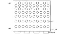
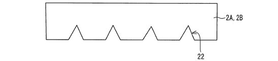
- FIG. 6 is a plan view showing the back surface of the light guide plates 2A and 2B subjected to dot processing.
- a plurality of dots 21 are formed on the back surfaces of the light guide plates 2A and 2B.
- each of the plurality of dots 21 has a hemispherical shape.
- the plurality of dots 21 On the back surface of the light guide plate 2A, the plurality of dots 21 have a low density from the side surface on the side where the light source 4A is arranged to the opposite side surface (side surface far from the light source 4A) facing the side surface. It is formed so as to be dense.
- a plurality of dots 21 has a density from the side surface on the side where the light source 4B is disposed to the opposite side surface (side surface far from the light source 4A) facing the side surface. Is formed from sparse to dense.
- the light incident on the light guide plate 2A from the light source 4A can be sequentially reflected by the plurality of dots 21 arranged on the back surface of the light guide plate 2A and can be incident on the optical path changing member 1.
- the light incident on the light guide plate 2B from the light source 4B can be sequentially reflected by the plurality of dots 21 arranged on the back surface of the light guide plate 2B and can be incident on the optical path changing member 1.
- BL unit 20 can be obtained.
- processing of the back surface of the light guide plates 2A and 2B is not limited to the hemispherical dots 21, but may be a prism shape (triangular pyramid shape) having a triangular cross section as shown in FIG.
- FIG. 7 is a cross-sectional view of the light guide plates 2A and 2B having prism-shaped processing formed on the back surface.
- an injection molding method in which the light guide plates 2A and 2B are formed by injection molding using a concavo-convex mold, or A pattern printing method in which a light guide member having a flat surface in advance is formed by injection molding or cast method, and dedicated ink is printed so as to make projections by screen printing can be exemplified.
- an injection molding method is generally used because it has a short tact and can be manufactured at low cost.
- the pattern printing method is generally used instead of the injection molding method because of the residual stress of the resin and the fact that cost merit cannot be achieved compared to the small size. Has been adopted.
- an uneven pattern is formed in order to form an uneven pattern in consideration of the effect of light reflected from the side facing the light source arranged on the side (the side far from the light source).
- the pattern density balance can be made relatively uniform in the plane.
- a light source is arranged on each of the opposing side surfaces of one light guide plate, and the density of the uneven pattern in the vicinity of one light source side is made sparse like the above uneven pattern, and the other light source
- the density of the uneven pattern in the vicinity of the side is made dense, the characteristics of light emitted from the light guide plate in different directions are different, and in-plane uniformity in perspective cannot be achieved.
- the BL unit 20 has different light guide plates 2A and 2B, the uneven and sparse / dense patterns arranged on the back surface are respectively optimized, and the outgoing light A (FIG. 3) is obtained. ) And outgoing light B (FIG. 3) can have the same characteristics.
- the reflecting plate 3 is a light reflecting member that reflects the light leaked from the bottom surface SUF5A of the light guide plate 2A.
- the surface shape of the reflecting plate 3 is a flat shape.
- the reflection plate 3 has a plate shape in this embodiment, but is not limited to a plate shape, and various shapes can be used.
- a film made of a polyester resin or a polyolefin resin, or a white film is used as a constituent material of the reflecting plate 3.
- a pigment such as titanium oxide, barium sulfate, calcium carbonate, aluminum hydroxide, magnesium carbonate, aluminum oxide is added to the plastic resin so as to be white. It is formed into a film or sheet. It is also possible to use a resin in which an inorganic filler such as calcium carbonate or titanium oxide is contained, a film is formed, and this is stretched to form a large number of microvoids.
- the light source 4A is provided at a position where light is emitted from the B side to the light guide plate 2A.
- the light source 4B is provided at a position where light is emitted from the A side to the light guide plate 2B. That is, as shown in FIG. 3, the light sources 4A and 4B are arranged on the left and right sides with respect to the paper surface.
- the direction in which the light from the light source 4A is emitted is the right direction (emitted light A in FIG. 3), and the direction in which the light from the light source 4B is emitted is the left direction (emitted light B in FIG. 3).
- the light sources 4A and 4B LEDs (Light Emitting Diodes) are used in the present embodiment, but a CCFT (Cold Cathode Fluorescent Tube) or a surface light source such as electroluminescence may be used. good.
- the light source is assumed to be at least two independent LEDs.
- the light sources 4A and 4B are CCFT, a U-shaped fluorescent tube may be used, and the single light tube in which the light source 4A and the light source 4B are connected to each other may be used.
- two L-shaped fluorescent tubes may be used in combination.
- the light sources 4A and 4B may include a reflector (not shown).
- the inner surface of the reflector has a parabolic shape, and the light sources 4A and 4B are arranged at the focal position.
- the liquid crystal panel 5 is a display panel that can simultaneously display a plurality of images. As shown in FIG. 3, the liquid crystal panel 5 has a light irradiation surface SUF3 to which light emitted from the light emission surface SUF4B of the light guide plate 2B is directly irradiated.
- the liquid crystal panel 5 is arranged in order from the front side to the back side.
- the polarizing plate 51, the parallax barrier (parallax barrier) 52, the adhesive layer 53, the CF (color filter) substrate 54, the TFT (thin film transistor) substrate 55, the polarization A plate 56 is provided.
- a liquid crystal layer (not shown) is arranged between the CF substrate 54 and the TFT substrate 55.
- the back surface of the display area located on the A side (the right side of the drawing) in the liquid crystal panel 5 is illuminated by light emitted from the optical path changing member 1 from the light source 4A through the light guide plates 2A and 2B.
- a luminance peak is obtained at a viewing angle of 45 degrees.
- the back surface of the display area located on the B side (the left side of the drawing) in the liquid crystal panel 5 is illuminated by light emitted from the optical path changing member 1 from the light source 4B through the light guide plate 2B.
- a luminance peak is obtained at a viewing angle of ⁇ 45 degrees.
- the luminance peak for the image displayed on the A side of the liquid crystal panel 5 and the luminance peak for the image displayed on the B side of the liquid crystal panel 5 are in different directions.
- the viewing angle at which the luminance peak can be obtained for each of the images displayed on the A side and the B side of the liquid crystal panel 5 can be set to a desired angle. It is possible to improve the display quality of the image.
- polarizing plates 51 and 56 are composed of a polarizing substrate containing a polarizing element, a base substrate (not shown) sandwiching the polarizing substrate between both sides, a protective film (not shown) on one side, and a polarizing plate on the other side. It is comprised from the release film (not shown) for affixing on a glass substrate.
- the polarizing plates 51 and 56 are as thin as about 0.12 mm to 0.4 mm even if about 10 layers are stacked.
- a polarizing substrate containing a polarizing element is iodine or a dichroic dye that is a polarizing element, which causes a polarizing effect.
- As the polarizing substrate polyvinyl alcohol (PVA, Poly Vinyle Alcohol) is used, and the polarizing element is included in this medium.
- Triacetyl cellulose (TAC, Triacetyl cellulose, Cellulose triacetate) is used as a base substrate for protecting the polarizing substrate.
- the release film is coated with an adhesive layer on the base substrate side, peeled off when applied to the glass substrate, and attached to the glass substrate with the adhesive layer.
- parallax barrier 52 Next, the parallax barrier 52 will be described with reference to FIGS.
- the parallax barrier 52 is an optical member in which a light transmission region and a blocking region are formed in a stripe shape, and the parallax barrier 52 separates a plurality of images to be displayed into individual display regions.
- FIG. 8 is a plan view of the liquid crystal panel 5 provided with a parallax barrier.
- FIG. 9 is a diagram illustrating how light is emitted to the A side and the B side of the liquid crystal panel 5.
- the parallax barrier 52 covers the right half of the pixels in the odd lines and the left half of the pixels in the even lines.
- An even line pixel in which the left half is covered with the parallax barrier 52 and the right half is exposed is referred to as a pixel 57A
- an odd line pixel in which the right half is covered with the parallax barrier 52 and the left half is exposed is referred to as a pixel 57B.
- the parallax barrier 52 covers half of the pixels, different images can be displayed on each of the pixels 57A and 57B (DV display), and different images can be viewed by the users on the A side and B side. .
- DV display can be performed by adjusting the parallax barrier 52 and the pixel configuration so that the viewing angle to the A side and the B side is ⁇ 45 degrees. Further, 3D display with the naked eye can be performed by adjusting the viewing angle to be ⁇ 6 degrees.
- the adhesive layer 53 shown in FIG. 3 is a transparent resin layer such as an acrylic resin that adheres the parallax barrier 52 and the CF substrate 54. Note that if the parallax barrier 52 and the CF substrate 54 are formed in contact with each other, the function as a parallax barrier cannot be exerted, so the adhesive layer 53 adjusts the distance between the parallax barrier 52 and the CF substrate 54 to an appropriate distance. This distance may be any distance that allows DV display.
- the CF substrate 54 shown in FIG. 3 has a colored layer or a black matrix (BM) that transmits red (R), green (G), and blue (B) light on the substrate in correspondence with each pixel. , Covered with a protective film.
- This colored layer is a coloring material or a colored film applied to the CF substrate 54 with a fine pattern, and a pigment-based or dye-based one is used.
- the BM layer prevents light leakage during black display and color mixing between adjacent colorants, and also prevents generation of photocurrent due to light irradiation to the TFT substrate 55.
- the photosensitive material is used for fixing the coloring material, it is mixed with the coloring material and fixed as it is.
- a thin BM layer of about 0.1 ⁇ m has a lot of metallic chromium, and carbon, titanium, nickel, etc. are also used.
- a high-definition screen has many stripe arrangements of colored layer patterns, but a low-definition screen has a good image quality with a good delta arrangement.
- the sensors 6A, 6B As shown in FIG. 1, the sensors 6 ⁇ / b> A and 6 ⁇ / b> B are provided on the front side of the liquid crystal panel 5, that is, the side on which the liquid crystal panel 5 displays an image, and are provided inside a frame frame 9 as a casing. Yes.
- the sensors 6A and 6B are luminance sensors that sense the luminance of light incident on the sensors 6A and 6B.
- the senor 6A is provided on the path of light emitted from the display area located on the left side (B side) of the liquid crystal panel 5.
- the sensor 6A measures the luminance of the light incident on it, and supplies the result of the measurement as detection data A to the calculation unit 7.
- the sensor 6B is provided on the path of light emitted from the display area located on the right side (A side) of the liquid crystal panel 5.
- the sensor 6B measures the luminance of the light incident on the sensor 6B, and supplies the result of the measurement to the calculation unit 7 as detection data B different from the detection data A.
- FIG. 10 is a block diagram illustrating a configuration of the display system 100 including the calculation unit 7.
- the calculation unit 7 includes a data analysis unit 71, a light source emission condition determination unit 72, and a calculation unit memory 73.
- the brightness of the incident light to the sensor 6A (left image IL in FIG. 2) is equal to the incident light to the sensor 6B (in FIG. 2).
- the luminance is higher than the luminance of the right image IR
- the data analysis unit 71 transmits a measurement command signal S_Enable_A to the sensor 6A.
- the data analysis unit 71 also transmits a measurement command signal S_Enable_B to the sensor 6B.
- the sensor 6A When the sensor 6A receives the measurement command signal S_Enable_A, the sensor 6A starts measuring the luminance, and transmits the measurement result to the data analysis unit 71 as detection data A.
- the sensor 6B receives the measurement command signal S_Enable_B, the sensor 6B starts measuring the luminance, and transmits the measurement result to the data analysis unit 71 as detection data B.
- the data analysis unit 71 receives the detection data A and B.
- the data analysis unit 71 transmits the analysis result A obtained by subjecting the detection data A to AD (Analog-Digital) conversion and noise removal to the light source emission condition determination unit 72.
- the data analysis unit 71 transmits the analysis result B obtained by performing AD conversion and noise removal on the detection data B to the light source emission condition determination unit 72.
- the light source emission condition determination unit 72 receives the analysis result A and the analysis result B.
- the light source emission condition determination unit 72 compares the brightness value measured by the sensor 6A indicated by the analysis result A and the brightness value measured by the sensor 6B indicated by the analysis result B.
- the luminance value measured by the sensor 6A indicated by the analysis result A is measured by the sensor 6B indicated by the analysis result B. It is larger than the brightness value.
- the calculation unit memory 73 is constituted by, for example, a ROM (Read Only Memory).
- a look-up table indicating the relationship between the result of the above-described size comparison and the increase / decrease in the current value applied to the light sources 4A and 4B is recorded in advance.
- the light source emission condition determination unit 72 reads the lookup table from the calculation unit memory 73.
- the look-up table includes information indicating that, when the luminance value indicated by the analysis result A is greater than the luminance value indicated by the analysis result B, the current value applied to the light source 4A is reduced by a predetermined value. It is out.
- the look-up table includes information indicating that when the luminance value indicated by the analysis result A is smaller than the luminance value indicated by the analysis result B, the current value applied to the light source 4A is increased by a predetermined value. Is included.
- the light source emission condition determination unit 72 controls the light emission condition setting value A to decrease or increase the current value applied to the light source 4A by a predetermined value according to the information included in the lookup table. Transmit to unit 8.
- the light emission condition setting value A is obtained by preliminarily setting the current value to be applied to the light source 4A to the light source drive control unit 8. The value is decreased by a predetermined value.
- the light emission condition setting value A is set in advance to the current value applied to the light source 4A to the light source drive control unit 8. The value is increased by a predetermined value.
- the light emission condition setting value A is the current applied to the light source 4A to the light source drive control unit 8. The value is reduced by a predetermined value.
- the look-up table includes information indicating that when the luminance value indicated by the analysis result A is larger than the luminance value indicated by the analysis result B, the current value applied to the light source 4B is increased by a predetermined value. May be included.
- the look-up table includes information indicating that when the luminance value indicated by the analysis result A is smaller than the luminance value indicated by the analysis result B, the current value applied to the light source 4B is decreased by a predetermined value. May be included.
- the light source light emission condition determining unit 72 uses the same principle as the light emission condition setting value A for increasing or decreasing the current value applied to the light source 4A, and the light emission condition setting value B for increasing or decreasing the current value applied to the light source 4B. Is transmitted to the light source drive control unit 8.
- the light source drive control unit 8 receives the light emission condition setting value A or the light emission condition setting value B.
- the light source drive control unit 8 can be constituted by, for example, a general LED drive circuit that drives the light sources 4A and 4B by supplying current to the light sources 4A and 4B.
- the light source drive control unit 8 can easily generate the light source control signal A, which is the current applied to the light source 4A, based on the light emission condition setting value A. That is, in this example, the light source drive control unit 8 may reduce the current value of the light source control signal A based on the light emission condition setting value A.
- the light source drive control unit 8 can easily generate the light source control signal B, which is the current applied to the light source 4B, based on the light emission condition setting value B. That is, in this example, the light source drive control unit 8 may increase the current value of the light source control signal B based on the light emission condition setting value B.
- the difference between the luminance value indicated by the analysis result A and the luminance value indicated by the analysis result B is a certain value (for example, the current value applied to the light source 4A or 4B in one operation).
- the value is less than the value to be increased or decreased, the operation is terminated.
- the difference between the brightness value indicated by the analysis result A (the brightness value measured by the sensor 6A) and the brightness value indicated by the analysis result B (the brightness value measured by the sensor 6B) refer to the analysis results A and B. Then, the light source emission condition determination unit 72 may obtain it.
- the drive control of the light sources 4A and 4B described above is current control in which the amplitude of the current applied to each of the light sources 4A and 4B is variable.
- PWM Pulse Width Modulation
- the display system 100 can achieve the same effect as that in the case where the drive control described above is performed even when the drive control of the light sources 4A and 4B is PWM. Such PWM control will be described.
- the calculation unit memory 73 the result of comparing the brightness value indicated by the analysis result A and the brightness value indicated by the analysis result B, and the pulse applied to the light sources 4A and 4B during one cycle.
- a look-up table showing the relationship with width expansion and contraction is recorded in advance.
- the “pulse width during one period of current” is simply referred to as “current pulse width”.
- the light source emission condition determination unit 72 reads the lookup table from the calculation unit memory 73.
- the look-up table includes information indicating that when the luminance value indicated by the analysis result A is greater than the luminance value indicated by the analysis result B, the pulse width of the current applied to the light source 4A is reduced by a predetermined width. Contains. Further, the lookup table indicates that when the luminance value indicated by the analysis result A is smaller than the luminance value indicated by the analysis result B, the pulse width of the current applied to the light source 4A is extended by a predetermined width. Contains information.
- the light source light emission condition determination unit 72 performs light source drive control on the light emission condition setting value A that expands or contracts the pulse width of the current applied to the light source 4A by a predetermined width according to the information included in the lookup table. Transmit to unit 8.
- the light emission condition setting value A indicates the pulse width of the current applied to the light source 4A to the light source drive control unit 8. , A value to be reduced by a predetermined width.
- the light emission condition setting value A indicates the pulse width of the current applied to the light source 4A to the light source drive control unit 8. , A value that extends by a predetermined width.
- the look-up table indicates that when the luminance value indicated by the analysis result A is larger than the luminance value indicated by the analysis result B, the pulse width of the current applied to the light source 4B is extended by a predetermined width. Information may be included.
- the lookup table indicates that when the luminance value indicated by the analysis result A is smaller than the luminance value indicated by the analysis result B, the pulse width of the current applied to the light source 4B is reduced by a predetermined width.
- Information may be included.
- the light source light emission condition determining unit 72 uses the same principle as the light emission condition setting value A for expanding and contracting the pulse width of the current applied to the light source 4A, and the light emission condition setting value B for expanding and contracting the pulse width of the current applied to the light source 4B. Is transmitted to the light source drive control unit 8.
- the light source drive control unit 8 receives the light emission condition setting value A or the light emission condition setting value B.
- the light source drive control unit 8 can be configured by, for example, a general LED drive circuit that drives the light sources 4A and 4B by supplying a current subjected to PWM modulation to the light sources 4A and 4B.
- the light source drive control unit 8 can easily generate the light source control signal A, which is the current applied to the light source 4A, based on the light emission condition setting value A. That is, the light source drive control unit 8 may expand or contract the pulse width of the current of the light source control signal A based on the light emission condition setting value A.
- the light source drive control unit 8 can easily generate the light source control signal B, which is the current applied to the light source 4B, based on the light emission condition setting value B. That is, the light source drive control unit 8 may expand or contract the pulse width of the current of the light source control signal B based on the light emission condition setting value B.
- the difference between the luminance value indicated by the analysis result A and the luminance value indicated by the analysis result B is a certain value (for example, a value corresponding to the pulse width of the current that is expanded or contracted by one operation). ) When it becomes less than, the operation is terminated.
- the difference between the brightness value indicated by the analysis result A (the brightness value measured by the sensor 6A) and the brightness value indicated by the analysis result B (the brightness value measured by the sensor 6B) refer to the analysis results A and B. Then, the light source emission condition determination unit 72 may obtain it.
- the display system 100 can achieve the effects described above even when the drive control of the light sources 4A and 4B is PWM.
- the light source drive control unit 8 may be configured to be able to read information recorded in the memory 10 and record information in the memory 10.
- the position where the memory 10 is provided may be in the backlight unit 300 or in another display device unit 200 (see FIG. 2).
- the solid state variation between the light source 4A and the light source 4B, the visual characteristics of the liquid crystal panel 5 are asymmetrical, the positional deviation of the parallax barrier 52, and the like.
- these luminances can be made substantially uniform.
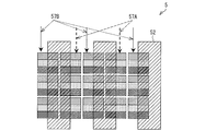
- FIG. 11 is a diagram showing a BL unit (backlight unit) 20c, which is still another configuration example of the backlight unit.
- the BL unit 20c is different from the BL unit 20 in that light sources are arranged along two sides (side surfaces) of the light guide plates 2A and 2B.
- light sources 4A and 4C are arranged on each of two adjacent sides of the light guide plate 2A.
- a light source is provided on each of the side facing the side where the light source 4A is disposed and the side facing the one side where the light source (first light source, second light source) 4C is disposed. Is not arranged.
- light sources 4B and 4D are arranged on each of the adjacent sides of the light guide plate 2B.
- the light source 4A, 4B, 4C, and 4D are arranged on each of the four sides (side surfaces) of the BL unit 20c when viewed in plan.
- the BL unit 20c it is possible to realize a backlight suitable for CV display in which different images are displayed in the four directions of left and right and up and down.
- the above-described optical characteristic ( ⁇ ⁇ ) has no direction dependency, or the direction from the left side to the right side (right side to left side) in plan view.
- the backlight unit of the present invention is a backlight unit having a light source and a light guide member in order to solve the above problems, and the light source and the light guide member are first and first, respectively.
- the first light source and the second light source are arranged opposite to each other via the first light guide member and the first light source member in plan view, and are arranged on the side surface of the optical member. 2 having an incident surface directly incident on the light emitted from the light guide member 2 and an output surface directly emitting the incident light from the incident surface toward the external display panel, and changing the optical path of the light passing therethrough
- An optical path changing member is provided.
- the first and second light sources arranged to face each other via the first and second light guide members, and the first light source arranged on the side surface are the first.
- first and second light sources opposed to each other through the first and second light guide members are provided in a plan view, even if the size is increased, the distance between both side surfaces opposed in the plan view Can be prevented from changing, and display quality can be prevented from deteriorating.
- the first and second light guide members are preferably arranged so as to overlap each other in plan view.
- a plurality of uneven shapes are formed on the back surfaces of the first and second light guide members, and the plurality of uneven shapes are formed on the back surface of the first light guide member.
- the density is formed from sparse to dense, and on the back surface of the second light guide member, It is preferable that the density be formed from sparse to dense from the side surface on the side where the second light source is disposed to the opposite side surface facing the side surface.
- the light path is changed by sequentially reflecting the light incident on the first light guide member from the first light source by the plurality of uneven shapes arranged on the back surface of the first light guide member.
- the light is incident on the member, and the light incident on the second light guide member from the second light source is sequentially reflected by the plurality of concave and convex shapes disposed on the back surface of the second light guide member, so that the optical path It can enter into a change member.
- the uneven shape may be a hemispherical shape or a triangular pyramid shape.
- a plurality of prism rows are formed on the emission surface of the optical path changing member, and the axis of each prism row is perpendicular to the emission directions of the first and second light sources.
- the emission angle of the emitted light when the light incident on the optical path changing member at a predetermined incident angle along the emission direction of the first and second light sources is emitted from the emission surface is It becomes smaller than the incident angle. For this reason, a backlight unit having luminance directivity in a plurality of different directions can be obtained.
- the optical path changing member preferably includes scattering fine particles that scatter light.
- the total light transmittance and the haze value are adjusted to desired values by appropriately adjusting the constituent material of the base material, the constituent material of the scattering fine particles, the average particle diameter (particle diameter), and the mixing rate. can do.
- the above optical characteristics have no direction dependency, but conversely, it can be said that the above optical characteristics are provided isotropically.
- CV display a backlight unit suitable for so-called quartet view display
- the display device of the present invention the backlight unit, the display panel that displays information on the display screen by receiving light emitted from the emission surface of the optical path changing member provided in the backlight unit, It is preferable to provide.
- the display panel has at least two luminance sensors that are installed in at least two directions different from the normal direction of the display screen and detect the luminance of light emitted from the display screen, and the two luminance sensors.
- a light source drive control unit that adjusts the magnitude of the current supplied to each of the first and second light sources so that the difference in luminance between the detected lights is smaller than a predetermined luminance difference. Preferably it is.
- the light source drive control unit supplies the current to each of the first and second light sources so that the difference in luminance between the lights detected by the two luminance sensors is smaller than the predetermined luminance difference. Adjust the size of. Therefore, it is possible to suppress in-plane luminance variations caused by variations in the first and second light sources.
- the present invention can be used for a backlight unit or a display device that requires the backlight unit.
- Optical path changing member 1a Diffusion sheet (optical path changing member) 1b Lens sheet (optical path changing member) 1c Prism row 2A
- Calculation unit 8 Light source drive control unit 20 BL unit (backlight unit) 20c BL unit (backlight unit) 21 dots (multiple irregular shapes)
- 100 Display system (display device) SUF1 Light incident surface (incident surface) SUF2 light exit surface (exit surface) SUF4A light exit surface SUF4B light exit surface SUF5A bottom surface SUF5B bottom surface
Landscapes
- Physics & Mathematics (AREA)
- General Physics & Mathematics (AREA)
- Optics & Photonics (AREA)
- Engineering & Computer Science (AREA)
- Computer Hardware Design (AREA)
- Theoretical Computer Science (AREA)
- Planar Illumination Modules (AREA)
Abstract
BLユニット(20)は、光源(4A・4B)、導光板(2A・2B)を備え、光源(4A)は導光板(2A)の側面に配されており、光源(4B)は導光板(2B)の側面に配されており、光源(4A・4B)は、平面視で、導光板(2A・2B)を介して対向配置されており、さらに、導光板(2A)又は導光板(2B)からの出射光を直接入射する光入射面(SUF1)と、光入射面(SUF1)からの入射光を、外部の液晶パネル(5)に向けて直接出射する光出射面(SUF2)とを有し、通過する光の光路を変更する光路変更部材(1)を備えている。これにより、大型化しても表示品位が劣化せず、かつ、複数の異なる方向へ輝度指向性を有する光を出射させる。
Description
本発明は、バックライトユニット及び表示装置に関する。
近年、液晶表示装置に代表される薄型、軽量、および低消費電力の表示装置が盛んに活用されている。こうした表示装置は、例えば携帯電話、スマートフォン、またはラップトップ型パーソナルコンピュータへの搭載が顕著である。また、今後はより薄型の表示装置である電子ペーパーの開発および普及も急速に進むことが期待されている。
このような状況の中、現在、単一のディスプレイから複数の異なる画像を視認させることを目的とした、いわゆるデュアルビューディスプレイ(以下、「DVディスプレイ」と略称する)の開発も積極的に進められている。DVディスプレイは、2つの異なる画像を同時に表示することができ、各画像は特定の方向からによってのみ見ることができるようになっている。
したがって、DVディスプレイから出射される出射光は、上記各画像を視認することが可能な方向に輝度指向性を有していることが望ましい。
また、液晶パネルは、パネルを構成する画素自体は発光しないので、液晶パネルからの出射光の輝度指向性は、バックライトから出射されるバックライト光の輝度指向性に大きく依存する。
しかし、図13に示すように、一般的に、バックライトは、表示ディスプレイ1000の正面方向(図14の視野角0°)に輝度指向性を有している。
一方、DVディスプレイで表示されるデュアルビュー表示(以下、「DV表示」という)は視野角が±45°方向への表示が中心である。
このため、図14に示す視野角0度の方向に輝度指向性を有するバックライトユニットをDV表示に用いた場合、バックライト光の輝度は、視野角±45度付近では60%程度も低下してしまい表示品位の劣化の原因となるという問題点がある。また、視野角±45度付近で輝度を高くするには、全体的にバックライトの輝度を高くする必要があり、バックライトの消費電力が不必要に増加してしまうという問題点がある。
そこで、特許文献1には、DVディスプレイ用のバックライトユニット(以下、単に「DVバックライトユニット」と称する)が開示されている。
これについて、図14を用いて説明する。
図14は、従来のDVバックライトユニットの構成を表す斜視図である。
DVバックライトユニットのうち、液晶パネル(不図示)が配される方向を表面側、反対側を裏面側とすると、DVバックライトユニットは、表面側から裏面側にかけて、順に配されている、プリズムシート1015、プリズムシート1014、拡散シート1013、導光板1012、及び反射板1016を備えている。さらに、導光板1012の4辺のうち一辺に沿って、光源1011が複数配されている。
また、プリズムシート1014のプリズム形成面は、導光板1012が配されている側に向き、かつそのプリズム軸(プリズムの稜線)は、液晶画面の上下方向に沿って平行に配置されている。
そして、プリズムシート1015のプリズム形成面は、液晶パネル側に向き、かつそのプリズム軸は、液晶画面の左右方向と一致するように配置されている。
光源1011から発光された光は、導光板1012の一側面から導光板1012内に入射し、当該入射光は導光板1012の一面から面状に出射する。
導光板1012にからの出射光は、拡散シート1013を介して入射する、2枚のプリズムシート1014・1015により、2方向に輝度指向性を有する光に変換され、DV表示可能な液晶パネルへ入射する。
このように、図14のDVバックライトユニットによると、左右の2方向において高い輝度を得ることが可能となっている。
さらに、近年では、設計の簡素化や、製造設備の維持にかかるコストの低減化を実現するために、小型、中型、大型を問わず、共通した構成のバックライトユニットが好ましい。
図14で示したDVバックライトユニットによると、光源1011は、一つの導光板1012の一辺に沿って配されている。
このため、DVバックライトを大型化(大面積化)すると、導光板1012のうち、光源1011が配されている側とは逆側の端部からは、導光板1012内で複数回の反射を繰り返した光が出射することとなる。一般的に、白色光は、複数回の反射を繰り返すと、低波長側の輝度が低下する。
このため、図14に示したDVバックライトユニットでは、大型化すると、導光板1012から面状に発光された光のうち、光源1012近傍の光の色と、光源1012から離れた側面近傍の光の色とでは異なることとなり、表示品位が劣化する原因となる。
本発明は、上記の問題点に鑑みなされたものであって、その目的は、大型化しても表示品位が劣化せず、かつ、複数の異なる方向へ輝度指向性を有する光を出射させることである。
本発明のバックライトユニットは、上記の課題を解決するために、光源及び導光部材を有するバックライトユニットであって、上記光源及び導光部材は、それぞれ、第1及び第2の光源、第1及び第2の導光部材を備え、上記第1の光源は、上記第1の導光部材の側面に配されており、上記第2の光源は、上記第2の導光部材の側面に配されており、上記第1及び第2の光源は、平面視で、上記第1及び第2の導光部材を介して対向配置されており、さらに、上記第1又は第2の導光部材からの出射光を直接入射する入射面と、当該入射面からの入射光を、外部の表示パネルに向けて直接出射する出射面とを有し、通過する光の光路を変更する光路変更部材を備えていることを特徴としている。
上記構成によると、平面視で、上記第1及び第2の導光部材を介して対向配置されている第1及び第2の光源と、側面に第1の光源が配されている第1の導光部材と、側面に第2の光源が配されている第2の導光部材と、通過する光の光路を変更する光路変更部材とを備えている。
これにより、上記表示パネルの表示画面の法線方向とは異なる少なくとも2つの方向の輝度分布が極大となる輝度指向性を有する光を、上記光路変更部材の出射面から出射することができる。
さらに、平面視で、上記第1及び第2の導光部材を介して対向配置されている第1及び第2の光源を備えているので、大型化しても、平面視で対向する両側面間の色が変化することを防止することができ、表示品位の劣化を防止することができる。
本発明のバックライトユニットは、光源及び導光部材を有するバックライトユニットであり、上記光源及び導光部材は、それぞれ、第1及び第2の光源、第1及び第2の導光部材を備え、上記第1の光源は、上記第1の導光部材の側面に配されており、上記第2の光源は、上記第2の導光部材の側面に配されており、上記第1及び第2の光源は、平面視で、上記第1及び第2の導光部材を介して対向配置されており、さらに、上記第1又は第2の導光部材からの出射光を直接入射する入射面と、当該入射面からの入射光を、外部の表示パネルに向けて直接出射する出射面とを有し、通過する光の光路を変更する光路変更部材を備えている。
これにより、大型化しても表示品位が劣化せず、かつ、複数の異なる方向へ輝度指向性を有する光を出射させることができるという効果を奏する。
本発明の一実施形態について図1~図12に基づいて説明すれば、次の通りである。以下の特定の項目で説明する構成以外の構成については、必要に応じて説明を省略する場合があるが、他の項目で説明されている場合は、その構成と同じである。また、説明の便宜上、各項目に示した部材と同一の機能を有する部材については、同一の符号を付し、適宜その説明を省略する。
(表示システム100の構成)
まず、図1、2を用いて、本発明の一実施形態にかかる表示システム(表示装置)100の構成の概略について説明する。
まず、図1、2を用いて、本発明の一実施形態にかかる表示システム(表示装置)100の構成の概略について説明する。
図1は、表示システム100の全体構成を示す図である。図1に示すように、表示システム100は、画像表示領域を有する液晶パネル(表示パネル)5と、液晶パネル5を背面側から照明するBL(バックライト)ユニット20と、画像表示領域を開口して液晶パネル5及びBLユニット20を囲うフレーム枠9と、液晶パネル5からの出射光の光量を検出するセンサ(輝度センサ)6A・6Bとを備えている。
さらに、表示システム100は、センサ6A・6Bからの出力に応じて光源4A・4Bの光量を制御するための演算部7、光源駆動制御部8、及びメモリ10を備えている。
BLユニット20は、BLユニット20の出射面となる光路変更部材1と、導光板(第1の導光部材)2A及び導光板(第2の導光部材)2Bと、反射板(反射部材)3と、光源(第1の光源)4A及び光源(第2の光源)4Bとを備えている。BLユニット20は、後述するように、2つの異なる方向の輝度指向性を有するものである。
表示システム100は、2つ以上の画像を、異なる方向に同時に表示することが可能な表示システムである。
例えば、表示システム100は、2つの画像を同時に表示するデュアルビュー表示(以下、DV表示と呼ぶ)、または、4つの画像を同時に表示するカルテットビュー表示(以下、CV表示と呼ぶ)が可能である。
本願明細書では、表示システム100は、主にDV表示か可能な表示システムであるものとして説明する。
図2は、表示システム100のDV表示の様子と、当該表示された画像の輝度の様子を表している。
図2の(a)に示すように、表示システム100は、右側から表示システム100を見た場合に視認できる右側画像IRと、左側から表示システム100を見た場合に視認できる左側画像ILとを両方、同時に表示が可能である。なお、本願明細書では、右側画像IRの側(紙面右側)を「A側」、左側画像ILの側(紙面左側)を「B側」と称する場合がある。
図2の(b)に示すように、表示システム100から出射される光は、真正面方向(視野角0度の方向)での輝度を抑えつつ、視野角が±45度でそれぞれ輝度がピークとなるように構成されている。
なお、本願明細書では、表示システム100を真正面方向から見る場合の角度を視野角0度とし、視野角0度からA側の視野角を+としており、視野角0度からB側の視野角を-として表現する。
このため、表示システム100では、表示品位がよい画像である、右側画像IRをA側のユーザへ、左側画像ILをB側のユーザへ、それぞれ視認させることができる。
さらに、表示システム100は、DV表示やCV表示に限定されず、3D(立体)表示が可能であってもよい。例えば、DV表示用の表示システム100から、視差バリアと画素構造との関係を調整することで、3D用メガネを用いない裸眼用の3D表示が可能な表示システムを得ることができる。
以下では、一例として、表示システム100は、主に、DV表示が可能な表示システムであるものとして説明する。以下、表示システム100の各構成要素について、順に説明していく。
(BLユニット20の全体構成)
図3、4を用いて、BLユニット20について説明する。
図3、4を用いて、BLユニット20について説明する。
図3は、液晶パネル5及びBLユニット20の構成を表す断面図である。
図3に示すように、BL(バックライト)ユニット20は、光路変更部材1、導光板(第1の導光部材)2A、導光板(第2の導光部材)2B、反射板(反射部材)3、及び光源(第1の光源)4A、光源(第2の光源)4Bを備えている。
ここで、本願明細書において「正面」とは、液晶パネル5が画像を表示する側(すなわち、ユーザが液晶パネル5を見る側)の面を意味している。一方、本願明細書において「背面」とは、液晶パネル5が画像を表示する側の反対側の面を意味している。
BLユニット20は、正面側から背面側へかけて順に、液晶パネル5、光路変更部材1、導光板2B、導光板2A、及び反射板3が配されて構成されている。
そして、導光板2Aの側面に光源4Aが配されており、導光板2Bの側面に光源4Bが配されている。
光源4Aは、導光板2Aの一辺(側面)に配されており、光源4Bは、導光板2Bの一辺(側面)に配されている。そして、光源4A・4Bは、BLユニット20を平面視したとき、導光板2A・2Bを介して対向配置されている。
なお、導光板2A・2Bは、導光板2Aが正面側に配され、導光板2Bが背面側に配されていてもよい。
このようにBLユニット20は、平面視したとき、導光板2A・2Bを介して対向配置されている光源4A・4Bと、一辺に光源4Aが配されている導光板2Aと、一辺に光源4Bが配されている導光板2Bと、通過する光の光路を変更する光路変更部材1とを備えている。
これにより、液晶パネル5の表示画面の法線方向とは異なる少なくとも2つの方向の輝度分布が極大となる輝度指向性を有する光を(出射光A・B)、光路変更部材1の光出射面(出射面)SUF2から出射することができる。
ここで、サイドライト型のバックライトは、導光体の側面から光源光を入射し、当該入射した光を内部で反射させて、導光体の出射面から面状に出射させるものである。
しかし、光を反射させていくと、次第に、低波長側の光強度が低下し、色味が変わってくる。
このため、特許文献1のように、導光体の一方の端面から入射させた光を面状に出射する導光体が一つだけでは、大型化(大面積化)すると、面内で光の色が変化してしまう。
そこで、2方向に輝度指向性を有するようにバックライトユニットの構成として、一つの導光板の両側にそれぞれ光源を設ける構成を考えることができる。
図12は、互いに対向する側面のそれぞれに光源504A・504Bが配された導光板の様子を表す側面図である。図12の(a)は、紙面右側から左側にかけて、凹凸パターンが疎から密となっている導光板の出射光の様子を表し、(b)は中央部分から両側面にかけて凹凸パターンが密から疎となっている導光板の出射光の様子を表し、(c)は紙面右側から左側にかけて、凹凸パターンが疎から密となっている大型の導光板の出射光の様子を表している。
図12の(a)~(c)に示す導光板502は、導光板502の互いに対向する両側面のうち、一方の側面側に光源504Aが配され、他方の側面側に光源504Bが配されている。
図12の(a)の導光板502の裏面には、光源504Bが配されている側の側面から、光源504Aが配されている側の側面にかけて、凹凸パターンが疎から密となるように配されている。
つまり、図12の(a)の導光板502では、光源Bから出射された出射光Bの面内輝度が均一となるように、凹凸パターンが形成されている。
まず、携帯電話やスマートフォン等、小型の表示装置に用いられるBLユニットの導光板について考える。
小型の導光板502の場合、光源504A・504Bからの出射光が、導光板502内で導光される光路が短い。
このため、小型の導光板502の場合、光源504B側に導光板502の凹凸パターンを合せたとしても(光源504B側が疎、光源504A側が密)、光源504Aから出射された光は、光源504Bが配されている側に近づくにつれ弱くはなるが、逆側側面に充分に届き、導光板502の光出射面から出射光Aとして出射させることができる。しかし、出射光Aの面内の輝度のバラツキが問題となる。
そこで、図12の(b)に示すように、導光板502の中央部分が密で、両側面に向かうにつれ疎となるように導光板502の凹凸パターンを調整する。すると、光源504Aから導光板502の光出射面から出射される出射光Aの面内の輝度バラツキと、光源504Bから導光板502の光出射面から出射される出射光Bの面内の輝度バラツキとを等しくすることができる。
このように、小型の場合は、導光板502の光路が短いので、一つの導光板であっても、導光板の凹凸パターンを調整することで、出射光Aと、出射光Bとのそれぞれの面内の輝度バラツキを調整することができる。
ここで、上述したように、白色の光は、導光板内で複数回の反射を繰り返すと、次第に低波長側の光量が減衰していき、色味が変わってくるので、導光板内での反射回数は少ない方が好ましい。
つまり、光源504A・504Bから導光板502内に入射した光は、順次、光出射面から出射光A・出射光Bとして出射していき、逆側の側面で反射されないことが好ましい。
しかし、小型では導光板502内での光路長が短い。このため、出射光A・Bの面内の輝度バラツキを均一にしつつ、さらに、光源504A・504Bから入射した光を、逆側の側面までで全て導光板502の光出射面側に出射させることができない。このため、逆側の一部側面で反射する光が存在している。
しかし、例えば、15インチ未満のパネル用のバックライトのように、導光板のサイズが小型であれば、導光板502の内部での光路長が短いので、光源504A・504Bから導光板502内に入射した光が、逆側側面方向へ導光していく際の反射回数は少なく、光源504A・504Bのそれぞれの逆側側面で反射されることによる光の色味の変化は、さほど問題とならない。
このように、導光板のサイズが小型であれば、一つの導光板502であっても、凹凸パターンを調整することで、面内の輝度バラツキが抑えられ、かつ、色味の変化が問題ないレベルの出射光A・Bを出射させることができる。
一方、例えば、20インチ以上等の大型のパネルに用いられるバックライトの場合、導光板502内の光路が長くなる。
図12の(c)に示すように、大型の導光板502の裏面に、光源504Bが配されている側の側面から、光源504Aが配されている側の側面にかけて、凹凸パターンが疎から密となるように配したとする。
つまり、図12の(c)の導光板502のように、光源504Bから出射された出射光Bの面内輝度が均一となるように、凹凸パターンを形成したとする。
すると、小型の場合は導光板502の光路が短いので、出射光Aは、光源504Bが配されている側面まで到達していたが、大型の場合は導光板502の光路が長いので、出射光Aは、光源504Bが配されている側面まで到達しなくなり、出射光Aは面内で輝度のばらつきが生じる。
そこで、図12の(b)に示したように、大型の導光板502でも、凹凸パターンの中央部分を密とし、側面にかけて疎となるように凹凸パターンを調整することが考えられる。つまり、光源504A・504Bそれぞれからの導光板502への入射光が、それぞれの光源504A・504Bが配されている側面と逆側の側面で反射するように、導光板502の凹凸パターンを調整するとする。
しかし、この場合、光路長が長くなることで反射回数が多くなっていることに加えて、さらに、光源504A・504Bのそれぞれが配されている側面と逆側側面でも反射することとなり、出射光Aと、出射光Bとのそれぞれの面内の色味のバラツキが大きくなる。
このように、一つの導光板502では、出射光A・B両方の輝度のバラツキ及び色味のバラツキを抑えつつ、大型化したBLユニットを構成することはできない。
そこで、BLユニット20は、平面視したとき、導光板2A・2Bを介して対向配置されている光源4A・4Bを備えている。すなわち、平面視で対向する両側面に光源4A・4Bが配されているので、大型化(大面積化)しても、平面視で対向する両側面間の色が変化することを防止することができ、表示品位の劣化を防止することができる。
また、BLユニット20は、2つの導光板2A・2Bを備えており、導光板2A・2Bのそれぞれの凹凸パターンを個別に調整することができるので、出射光Aと、出射光Bとのそれぞれの面内の輝度バラツキ及び色味のバラツキを抑えることができる。
つまり、BLユニット20は、複数の導光板2Aと、導光板2Bとを備えているので、導光板2A・2Bのそれぞれの裏面の凹凸パターンを調整することで、出射光A・Bのそれぞれの輝度の面内バラツキを抑えつつ、色味の面内バラツキを防止することができる。
(光路変更部材1)
光路変更部材1は、導光板2からの出射光を反射、拡散、集光させるなどの役割を持ついわゆる光学シートの一種であるが、本実施形態の光路変更部材1は、少なくともその光学的特性により、透過する光の光路を変更する部材である。
光路変更部材1は、導光板2からの出射光を反射、拡散、集光させるなどの役割を持ついわゆる光学シートの一種であるが、本実施形態の光路変更部材1は、少なくともその光学的特性により、透過する光の光路を変更する部材である。
図3に示すように、光路変更部材1は、背面に対向して配されている導光板2Bからの出射光を直接入射する光入射面(入射面)SUF1と、光入射面SUF1からの入射光を、外部の液晶パネル5に向けて直接出射する光出射面(出射面)SUF2とを有している。
この、光入射面SUF1と光出射面SUF2とは、紙面に対して上下方向に互いに対向している。
光入射面SUF1は平坦であっても良いし、凹凸形状を有していてもよい。すなわち、BLユニット20は、複数の光源4A・4B及び複数の導光板2A・2Bを有することで、2方向の輝度指向性を有する構成としている。このため、図14に示したように、導光板1013に向かって凸形状であるプリズムシート1014を設ける必要はなく、光入射面SUF1を平坦な構成とすることができる。
または、平坦に限定されず、光入射面SUF1は凹凸形状を有していてもよい。
図4、5に示すように、光路変更部材(光学シート)1は、一例として、図4に示す拡散シート1aや、図5に示すレンズシート1bで構成することができる。
図4は、光路変更部材1として拡散シート1aを用いたBLユニット20の光の経路を表す図である。図5は、光路変更部材1としてレンズシート1bを用いたBLユニット20の光の経路を表す図である。
光路変更部材1は、図4、5に示すように、光路変更部材1の光出射面SUF2から出射する光の出射角Φを、導光板2Bの光出射面SUF4Bから出射する光の出射角θよりも小さくする光学的特性を有している(Φ<θ)。
このため、図4、5に示すように、光源4Aから発した光は、光出射面SUF2の法線に対して右側に(A側、例えば、視野角+45度)傾いた方向の輝度指向性を有するバックライト光を出射することが可能となっている。一方、光源4Bから発した光は、法線に対して左側に(B側、例えば、視野角-45度)傾いた方向の輝度指向性を有するバックライト光を出射することが可能となっている。
また、図3に示すように、光路変更部材1の光出射面SUF2から出射する光は、外部の液晶パネル5に直接照射される。
言い換えれば、BLユニット20では、液晶パネル5と、導光板2Bとの間のシート状部材は、光路変更部材1の1枚のみで構成している。よって、上記特許文献1に記載のDVバックライトユニットより、光路変更部材(すなわち、導光板2Bと液晶パネル5との間に存在する部材)が少なくなり、導光板2Bからの出射光の利用効率が高い。
(拡散シート1a)
次に、図4を用いて、光路変更部材1を、拡散シート1aで構成した場合について説明する。
次に、図4を用いて、光路変更部材1を、拡散シート1aで構成した場合について説明する。
図4の(a)は、光源4Aからの出射光が、導光板2Bの光出射面SUF4B及び拡散シート1aの光出射面SUF2が出射する様子を表しており、(b)は光源4Bからの出射光が、導光板2Bの光出射面SUF4B及び拡散シート1aの光出射面SUF2が出射する様子を表している。
図4に示す拡散シート1aは、シート表面(光入射面SUF1または光出射面SUF2)に微細な形状や内部に散乱物質が混入されており、一般的には、上記の光学的特性(Φ<θ)に方向依存性は無いが、特定の方向に対して上記の光学的特性を有するように構成することも可能である。
よって、拡散シート1aにおいて、上記の光学的特性に方向依存性を持たせる場合は、光源4A,4Bの出射方向(拡散シート1aの面内方向)に対して、上記の光学的特性を持たせることが好ましい。
一方、拡散シート1aは、上記の光学的特性に方向依存性が無い場合、後述するレンズシート1bよりも多少効果は劣るものの、逆に等方的に上記の光学的特性(Φ<θ)を備えているとも言えるので、後述するCV表示用の光路変更部材1として好適である(図7)。
図4の(a)に示すように、光源4Aから出射した光は、導光板2Aの側面から、導光板2A内に入射する。そして、当該入射光は、導光板2Aの光出射面SUF4Aから出射し、導光板2Bを通り、導光板2Bの光出射面SUF4Bから出射角θで出射し、当該出射光は拡散シート1aに入射する。
そして、拡散シート1aは、導光板2Bの光出射面SUF4Bから出射角θで出射された光を、光入射面SUF1から入射し、当該入射光の角度を替えて、光出射面SUF2から出射角Φ(Φ<θ)で出射し、当該出射光が液晶パネル5に直接出射する。
一方、図4の(b)に示すように、光源4Bから出射した光は、導光板2Bの側面から、導光板2B内に入射する。そして、当該入射光は、導光板2Bの光出射面SUF4Bから出射角θで出射し、当該出射光は拡散シート1aに入射する。
そして、拡散シート1aは、導光板2Bの光出射面SUF4Bから出射角θで出射された光を、光入射面SUF1から入射し、当該入射光の角度を替えて、光出射面SUF2から出射角Φ(Φ<θ)で出射し、当該出射光が液晶パネル5に直接出射する。
本実施形態の拡散シート1aは、基材(母材)としての透明樹脂と、この透明樹脂の中に分散された光散乱剤(散乱微粒子)から構成されている。
拡散シート1aに使用される透明樹脂としては、例えば、熱可塑性樹脂、熱硬化性樹脂などを用いることができ、例えば、ポリカーボネート樹脂、アクリル系樹脂、フッ素系アクリル樹脂、シリコーン系アクリル樹脂、エポキシアクリレート樹脂、ポリスチレン樹脂、シクロオレフィンポリマー、メチルスチレン樹脂、フルオレン樹脂、ポリエチレンテレフタレート(PET)、ポリプロピレン、アクリルニトリルスチレン共重合体、アクリロニトリルポリスチレン共重合体などを用いることができる。
また、光散乱剤(散乱微粒子)としては、無機物または樹脂からなる透明微粒子を使用することができる。無機物からなる透明微粒子としては、例えば、シリカ(SiO2)、アルミナ(Al2O3)、酸化マグネシウム(MgO)、チタニアなどの酸化物からなる微粒子、または、炭酸カルシウム及び硫酸バリウムなどの他の微粒子を使用することができる。
樹脂からなる透明微粒子としては、アクリル樹脂、スチレン樹脂、アクリルスチレン樹脂若しくはそれらの架橋体;メラミンホルムアルデヒド樹脂;ポリテトラフルオロエチレン、ペルフルオロアルコキシ樹脂、テトラフルオロエチレン-ヘキサフルオロプロピレン共重合体、ポリフルオロビニリデン及びエチレンテトラフルオロエチレン共重合体などのフッ素樹脂;またはシリコーン樹脂からなる粒子を使用することができる。
ここで、可視光の波長が350nm~800nm程度であることから、平均粒子径(粒径)が可視光の波長と同じオーダー(すなわち100nmオーダー)である散乱微粒子は、光の散乱に寄与し得る。
逆に言うと、光散乱性を発現するためには、散乱微粒子の粒径が100nm以上である必要がある。また、光散乱性を好適に発現させるためには、個々の散乱微粒子の粒径は、可視光の波長よりも大きなオーダーであることが好ましく、1μm以上であることが好ましい。従って、散乱微粒子の平均粒径は1μm以上であることが好ましく、2μm程度であることがより好ましい。
また、拡散シート1aにおいて、光散乱性を発現するための微粒子は、透明樹脂中に5質量%程度混入されている。勿論、微粒子の混入比率は、所望する光散乱性の程度(例えばヘイズ値で規定される)によって多少異なるが、5質量%を大きく超えると、ヘイズ値が、いたずらに大きくなり、それに伴って光が拡散シート1a中を伝搬する距離が伸びて透過率が極端に低下してしまう。
ここで、光散乱剤として散乱微粒子を用いた場合には、拡散シート1aの厚さが0.1~5mmであることが好ましい。拡散シート1aの厚みが0.1~5mmである場合には、最適な光散乱性と輝度を得ることができ、光学特性上好ましい。これに対し、厚みが0.1mm未満の場合には、所望の光散乱性を発揮することはできず、5mmを超える場合には、樹脂量が多いため吸収による輝度低下が生じ好ましくない。
なお、本実施形態の拡散シート1aは、ヘイズ値が75%であり、全光線透過率は86%であるが、ヘイズ値は、70%以上であり、全光線透過率は、50%以上であることが好ましい。
これにより、導光板2の出射角θ=+70±5度のとき、拡散シート1aの出射角Φ=+45度を実現できる。
なお、透明樹脂として熱可塑性樹脂を用いた場合には、光散乱剤として気泡を用いても良い。熱可塑性樹脂の内部に形成された気泡の内部表面が光の乱反射を生じさせ、散乱微粒子を分散させた場合と同等以上の光散乱性を発現させることができる。そのため、拡散シート1aの膜厚をより薄くすることが可能となる。
このような拡散シート1aとして、白色PETや白色PPなどを挙げることができる。白色PETは、PETと相溶性のない樹脂や酸化チタン(TiO2)、硫酸化バリウム(BaSO4)、炭酸カルシウムのようなフィラーをPETに分散させた後、該PETを2軸延伸法で延伸することにより、該フィラーの周りに気泡を発生させて形成する。
なお、熱可塑性樹脂からなる拡散シート1aは、少なくとも1軸方向に延伸されていればよい。少なくとも1軸方向に延伸させれば、フィラーの周りに気泡を発生させることができるためである。
熱可塑性樹脂としては、例えば、アクリロニトリルポリスチレン共重合体、ポリエチレンテレフタレート(PET)、ポリエチレン-2、6-ナフレート、ポリプロピレンテレフタレート、ポリブチレンテレフタレート、シクロヘキサンジメタノール共重合ポリエステル樹脂、イソフタル酸共重合ポリエステル樹脂、スポログリコール共重合ポリエステル樹脂、フルオレン共重合ポリエステル樹脂等のポリエステル系樹脂、ポリエチレン、ポリプロピレン、ポリメチルペンテン、脂環式オレフィン共重合樹脂等のポリオレフィン系樹脂、ポリメチルメタクリレート等のアクリル樹脂、ポリカーボネート、ポリスチレン、ポリアミド、ポリエーテル、ポリエステルアミド、ポリエーテルエステル、ポリ塩化ビニル、シクロオレフィンポリマー、およびこれらを成分とする共重合体、またこれら樹脂の混合物などを用いることができ、特に限定されることはない。
光散乱剤として気泡を用いた場合には、拡散シート1aの厚さが25~500μmであることが好ましい。
拡散シート1aの厚さが25μm未満の場合には、シートのこし(強度)が不足し、製造工程やフレーム枠9内でしわを発生しやすくなるので好ましくない。また、拡散シート1aの厚さが500μmを超える場合には、光学的特性についてはとくに問題ないが、剛性が増すためロール状に加工しにくい、スリットが容易にできないなど、従来の拡散シートと比較して得られる薄さの利点が少なくなるので好ましくない。
(微細凹凸構造)
拡散シート1aは、その光入射面SUF1または光出射面SUF2に微細凹凸構造が形成されたものであってもよい。この微細凹凸構造を形成する方法としては、拡散シート1aを形成する際に共押出形成法、出射成形法により微細凹凸構造を賦型するための金型に圧力をかけることで密着させて、微細凹凸構造を転写する方法が挙げられる。
拡散シート1aは、その光入射面SUF1または光出射面SUF2に微細凹凸構造が形成されたものであってもよい。この微細凹凸構造を形成する方法としては、拡散シート1aを形成する際に共押出形成法、出射成形法により微細凹凸構造を賦型するための金型に圧力をかけることで密着させて、微細凹凸構造を転写する方法が挙げられる。
さらに、微細凹凸構造を形成する方法として、拡散シート1aの光入射面SUF1または光出射面SUF2に、UV(Ultra Violet)硬化樹脂等のような放射線硬化樹脂を用いて成形する手法も挙げられる。より具体的には、共押出法により拡散シート1aを板状部材として成形した後に、拡散シート1aの光入射面SUF1または光出射面SUF2に凹凸形状をUV成形することで微細凹凸構造を形成することができる。
光入射面SUF1または光出射面SUF2の表面状態は、凹凸を粗さで数値化することが多いが、ここでは、表面状態をヘイズ値と凹凸間隔Sm値(以下、「Sm値」と呼ぶ)で示す。ヘイズ値は、JIS K 7136で定義され、ヘイズメータを用いて、5回測定した時の平均値で表され、Sm値は、表面粗さ規格JIS B0601-2001で定義され、接触式表面粗さ計を用いて、カットオフ値2.0mmの条件で測定したときの平均値を意味する。
ヘイズ値は大きければ大きいほど、光入射面SUF1または光出射面SUF2での散乱が多くなり、逆に小さければ、表面散乱が少なくなる。同時にSm値は、小さければ、表面凹凸が細かくなる。ヘイズ値が20%未満であると、光の表面散乱が少なくなる。
同様にSm値が300μm未満であると、凹凸間隔は細かいが凹凸粗さが不十分となり、光の表面散乱が弱くなり、900μmを超えると、凹凸間隔が広く粗さも粗くなるため、光の表面散乱は強くなるが正面輝度の低下につながる。
さらには、光入射面SUF1または光出射面SUF2の表面粗さが規則的であると、表面粗さが不規則なものと比較して一定の散乱効果を得る上で有利となり、また、製造が容易となる。
そのヘイズ値の調整方法はいくつかあり、凹凸を物理的に賦型する場合は、金型の表面状態を調整し、射出成形や押出し成形時にインラインで転写させる方法や、成形後オフラインで熱プレスや研磨剤のブラストを行う方法がある。また、押出条件で光散乱剤をブリードアウトさせる場合は、散乱微粒子の濃度や粒径および散乱層の厚さで調整を行う。
押出法は押出機で熱可塑性樹脂を加熱溶融させ、Tダイから押出し、板状に成形する。共押出法は積層板の場合に用い、複数台の押出機を用い、フィードブロックダイやマニホールドダイなどの積層ダイから、積層押出しを行い、複層板状に成形する。
(レンズシート1b)
次に、図5を用いて、光路変更部材1を、レンズシート1bで構成した場合について説明する。
次に、図5を用いて、光路変更部材1を、レンズシート1bで構成した場合について説明する。
図5の(a)は、光源4Aからの出射光が、導光板2Bの光出射面SUF4B及びレンズシート1bの光出射面SUF2が出射する様子を表しており、(b)は光源4Bからの出射光が、導光板2Bの光出射面SUF4B及びレンズシート1bの光出射面SUF2が出射する様子を表している。
図5に示すように、レンズシート1bは、光出射面SUF2の側に複数のプリズム列1cが形成されている。
そして、レンズシート1bは、光出射面SUF2から出射する光の出射角Φを、導光板2Bの光出射面SUF4Bから出射する光の出射角θよりも小さくする光学的特性を有している。
具体的には、本実施形態のレンズシート1bでは、プリズム列1cの稜線(プリズムの軸)は、光源4A,4Bの出射方向に対して、垂直に配置されている。このため、光源4A,4Bから出射した光の伝搬方向に沿って所定の入射角でレンズシート1bに入射した光が光出射面SUF2側から出射するときの出射光の出射角Φの大きさは、導光板2Bの光出射面SUF4Bから出射する光の出射角θの大きさより小さくなる。
これにより、複数の異なる方向への輝度指向性を有するBLユニット20を構成している。
このプリズム列1c頂角の角度と、レンズシート1bの屈折率を調整することで、レンズシート1bからの出射角Φを制御することができる。
一例として、本実施形態のレンズシート1bでは、プリズム列1cの断面は、二等辺三角形状である。また、その頂角(プリズム頂角)は、80度~100度程度であり、屈折率は1.5程度である。
そして、導光板2Bの出射角θ=65±5度のとき、レンズシート1bの出射角Φ=45度を実現できる。なお、レンズシート1bの屈折率が大きくなるほど、出射角Φは0度に近づく。
(導光板2A・2B)
導光板2Aは、一方の端面に配されている光源4Aから出射した光を入射し、当該入射光を光出射面SUF4Aから出射し、導光板2Bを介して光路変更部材1の光入射面SUF1へ導光する部材である。
導光板2Aは、一方の端面に配されている光源4Aから出射した光を入射し、当該入射光を光出射面SUF4Aから出射し、導光板2Bを介して光路変更部材1の光入射面SUF1へ導光する部材である。
導光板2Bは、一方の端面に配されている光源4Bから出射した光を入射し、当該入射光を光出射面SUF4Bから出射し、光路変更部材1の光入射面SUF1へ直接導光する部材である。
より具体的には、導光板2A・2Bは、光源4A,4Bから発生した線状の光を、液晶パネル5へ入射するための面光源に変換する透明樹脂の板である。導光板2A・2Bの形状は、板状(直方体形状)であり、光出射面SUF4A・4B(底面SUF5A・5B)の形状は、矩形形状である。また、導光板2A・2Bの厚みは0.2mm~3mmであるが、導光板2A・2Bの厚みはこの範囲に限定されない。
光源4Aから導光板2Aに入射された光は、導光板2Aの光出射面SUF4Aから出射し、導光板2Bを透過し、例えば視野角θ=+70度±5度に相当する角度で、導光板2Bの出射面SUF4Bから出射される。一方、光源4Bから導光板2Bに入射された光は、例えば視野角θ=-70度±5度に相当する角度で、導光板2Bの光出射面SUF4Bから出射される(図4、5参照)。
一例として、20インチ以上の大型(大面積)のバックライトユニットを構成する場合、本実施の形態で説明したような、導光板2A・2Bを有するBLユニット20の構成とすることで、光路が長くなることによる低波長側の輝度の劣化を低減しつつ、出射光Aと、出射光Bとの輝度のバラツキを抑える効果を、特に、顕著に得ることができる。
なお、BLユニット20が対象とするパネルサイズは20インチより小さくてもよく、15インチ以上のパネルサイズに用いられるバックライトであれば、光路が長くなることによる低波長側の輝度の劣化を低減しつつ、出射光Aと、出射光Bとの輝度のバラツキを抑える効果を得ることができる。
導光板2A・2Bは、本実施形態では、板状であるが、楔形形状、船型形状などの種々の形状のものを使用できる。また、導光板2A・2Bの構成材料としては、メタクリル樹脂、アクリル系樹脂、ポリカーボネート系樹脂、ポリエステル系樹脂、塩化ビニル系樹脂等の透過率の高い合成樹脂を使用できる。導光板2A・2Bは、光出射面SUF4A・4Bが鏡面で、他方の底面SUF5A・5Bが粗面になったものを使用する。
導光板2A・2Bの底面SUF5A・5Bには、輝度均一化や輝度向上のため、プリズム(複数の凹凸形状)加工やドット(複数の凹凸形状)加工などが施されている。
導光板2A・2Bは、屈折率を調整したり、底面SUF5A・5Bに配されているプリズムパターンの配置や、ドットパターンの配置を調整したりすることで、2枚の導光板2A・2Bが重なっていたとしても、光源4Aからの出射光が、導光板2Bの光出射面SUF4Bから角度θで出射すると共に、光源4Bからの出射光が導光板2Bの光出射面SUF4Bから角度θで出射するようになっている。
図6は、ドット加工が施された導光板2A・2Bの裏面を表す平面図である。
図6に示すように、導光板2A・2Bのそれぞれの裏面には、複数のドット21が形成されている。一例として、複数のドット21のそれぞれは半球形状である。
導光板2Aの裏面には、複数のドット21が、光源4Aが配されている側の側面から、当該側面と対向する逆側の側面(光源4Aから遠い側の側面)にかけて、密度が疎から密となるように形成されている。
同様に、導光板2Bの裏面には、複数のドット21が、光源4Bが配されている側の側面から、当該側面と対向する逆側の側面(光源4Aから遠い側の側面)にかけて、密度が疎から密となるように形成されている。
これにより、光源4Aから導光板2Aに入射した光を、導光板2Aの裏面に配された複数のドット21で順次反射させて、光路変更部材1に入射させることができる。
また、光源4Bから導光板2Bに入射した光を、導光板2Bの裏面に配された複数のドット21で順次反射させて、光路変更部材1に入射させることができる。
このため、光源4A・4Bから、導光板2A・2Bのそれぞれに入射した光が、導光板2A・2B内のそれぞれでの反射回数を抑えることができるので、面内の色のバラツキが抑制されたBLユニット20を得ることができる。
また、導光板2A・2Bの裏面の加工は、半球形状のドット21に限定されず、図7に示すような断面が三角形であるプリズム形状(三角錐形状)であってもよい。
図7は、プリズム形状の加工が裏面に形成された導光板2A・2Bの断面図である。
一般的に、導光板2A・2Bの底面SUF5A・5Bに凹凸形状を形成する方法としては、凹凸をつけた金型を使用して射出成形により導光板2A・2Bを成形する射出成形方式、または、あらかじめ表面がフラットな導光部材を射出成型またはキャスト方式で成形し、スクリーン印刷にて突起をつけるよう専用インクを印刷するパターン印刷方式を例示できる。
小型である、面積が小さいの導光板を作成する場合は、タクトが短く、かつコストを安く製作することができる点から、一般的に射出成形方式が用いられている。
一方、大型である、面積が大きい導光板を作成する場合は、樹脂の残留応力や、小型に比べてコストメリットが出せないなどの理由から、射出成形方式ではなく、パターン印刷方式が、一般的に採用されている。
小型の導光板の場合は、側面に配された光源と対向する側の側面(光源から遠い側の側面)で反射する光の影響を考慮して、凹凸形状のパターンを形成するため、凹凸形状のパターンの密度バランスは、面内で比較的均一にすることができる。
一方、大型の導光板の場合、側面に配された光源と対向する側の側面(光源から遠い側の側面)で反射する光の影響は少なく、凹凸形状のパターンは光源から離れるほど密となる。
よって、一例として、一枚の導光板の対向する側面のそれぞれに光源を配し、上記の凹凸パターンのように、一方の光源側近傍での凹凸形状のパターンの密度を疎とし、他方の光源側近傍での凹凸形状のパターンの密度を密とすると、上記導光板から異なる方向に出射される光の特性がことなり、斜視での面内均一性を達成することはできない。
一方、BLユニット20によると、異なる導光板2A・2Bを有しているので、それぞれで、裏面に配されている凹凸形状の疎・密のパターンの最適化を行い、出射光A(図3)と出射光B(図3)との特性が同じになるようにすることができる。
このため、大型化しても、平面視で対向する両側面間の色が変化することを防止することができ、表示品位の劣化を防止することができる。
(反射板3)
図3に示すように、反射板3は、導光板2Aの底面SUF5Aから漏れた光を反射する光反射部材である。反射板3の表面形状はフラットな形状である。
図3に示すように、反射板3は、導光板2Aの底面SUF5Aから漏れた光を反射する光反射部材である。反射板3の表面形状はフラットな形状である。
反射板3は、本実施形態では板状であるが、板状に限定されず、種々の形状のものを使用できる。また、反射板3の構成材料としては、ポリエステル系樹脂もしくはポリオレフィン系樹脂からなるフィルム、または、白色フィルムを使用する。白色フィルムは、フィルムもしくはシート状に成形する前に、例えば、白色となるように、酸化チタン、硫酸バリウム、炭酸カルシウム、水酸化アルミニウム、炭酸マグネシウム、酸化アルミニウムなどの顔料をプラスチック樹脂に添加してフィルム、シートに成形したものである。樹脂に炭酸カルシウムや酸化チタン等の無機充填剤を含有させフィルムを成形し、これを延伸し多数のミクロボイドを形成させたものを使用することもできる。
(光源4A,4B)
図3に示すように、光源4Aは、B側から、導光板2Aに光を出射する位置に設けられている。光源4Bは、A側から、導光板2Bに光を出射する位置に設けられている。すなわち、光源4A,4Bは、図3に示すように、紙面に対して左右反対側に配置される。
図3に示すように、光源4Aは、B側から、導光板2Aに光を出射する位置に設けられている。光源4Bは、A側から、導光板2Bに光を出射する位置に設けられている。すなわち、光源4A,4Bは、図3に示すように、紙面に対して左右反対側に配置される。
また、光源4Aの光が出射される方向は、右方向(図3の出射光A)であり、光源4Bの光が出射される方向は、左方向(図3の出射光B)である。
これにより、バックライト面内における輝度の均一性と照射の配光角度分布を左右対称にすることができる。
また、光源4A,4Bとしては、本実施形態では、LED(Light Emitting Diode)を用いているが、CCFT(Cold Cathode Fluorescent Tube:冷陰極蛍光管)や、エレクトロルミネッセンス等の面光源を用いても良い。光源はここでは、少なくとも2つの独立したLEDであるものとしている。しかしながら、光源4A,4Bが、CCFTの場合、コ字状の蛍光管を採用し、光源4Aと光源4Bとが互いに繋がった1つの蛍光管であっても良い。また、光源4A,4Bとして、L字状の蛍光管を2本組み合わせて使用しても良い。
また、光源4A,4Bは、図示しないリフレクターを備えていても良い。リフレクターはその内面は放物線状の形状をなし、その焦点位置に光源4A,4Bが配置される。
(液晶パネル5)
液晶パネル5は、複数の画像を同時に表示することが可能な表示パネルである。図3に示すように、液晶パネル5は、導光板2Bの光出射面SUF4Bから出射された光が直接照射される光照射面SUF3を有している。
液晶パネル5は、複数の画像を同時に表示することが可能な表示パネルである。図3に示すように、液晶パネル5は、導光板2Bの光出射面SUF4Bから出射された光が直接照射される光照射面SUF3を有している。
液晶パネル5は、正面側から背面側にかけて順に配されている、偏光板51、視差バリア(パララックスバリア)52、接着層53、CF(カラーフィルタ)基板54、TFT(薄膜トランジスタ)基板55、偏光板56を備えている。また、CF基板54と、TFT基板55との間には、図示しない液晶層が配されている。
ここで、液晶パネル5における、A側(紙面右側)に位置する表示領域の背面は、光源4Aから導光板2A・2Bを通じて光路変更部材1から出射された光により照らされる。これにより、A側に位置する表示領域に表示される画像に関しては、視野角45度において、輝度のピークが得られる。
一方、液晶パネル5における、B側(紙面左側)に位置する表示領域の背面は、光源4Bから導光板2Bを通じて光路変更部材1から出射された光により照らされる。これにより、B側に位置する表示領域に表示される画像に関しては、視野角-45度において、輝度のピークが得られる。
以上の構成により、液晶パネル5のA側に表示される画像に対する輝度のピークと、液晶パネル5のB側に表示される画像に対する輝度のピークとが、互いに異なる方向となる。
従って、表示システム100では、液晶パネル5のA側およびB側に表示される画像の各々に関して、輝度のピークが得られる視野角を、所望の角度とすることが可能であるため、これらの各画像の表示品位を向上させることが可能である。
(偏光板51,56)
図3に示すように、偏光板51,56は、偏光素子が入った偏光基材とこれを両面で挟むベース基板(不図示)、そして片面には保護フィルム(不図示)ともう片面にはガラス基板に貼り付けるための離型フィルム(不図示)から構成される。
図3に示すように、偏光板51,56は、偏光素子が入った偏光基材とこれを両面で挟むベース基板(不図示)、そして片面には保護フィルム(不図示)ともう片面にはガラス基板に貼り付けるための離型フィルム(不図示)から構成される。
偏光板51,56は、多ければ10層ほど積層されても0.12mm~0.4mm程度の薄いものである。偏光素子が入った偏光基材とは、ヨウ素や二色性染料が偏光素子でありこれが偏光効果を起こす。偏光基材はポリビニルアルコール(PVA,Poly Vinyle Alcohol)が使用され、偏光素子がこの媒体内に含まれる。偏光基材を保護する役割のベース基板にはトリアセチルセルロース(TAC,Triacetyl cellulose, Cellulose triacetate)が使用される。離型フィルムにはベース基板側に粘着層が塗布されており、ガラス基板に貼り付ける段階で剥離され、粘着層によってガラス基板に貼り付けられる。
(視差バリア52)
次に、図8、9を用いて、視差バリア52について説明する。
次に、図8、9を用いて、視差バリア52について説明する。
視差バリア52は、光の透過領域と遮断領域とがストライプ状に形成された光学部材であり、視差バリア52により、表示すべき複数の画像を個々の表示領域に分離している。
図8は視差バリアが配された液晶パネル5の平面図である。図9は、液晶パネル5のA側、B側への光の出射の様子を表す図である。
図8に示すように、例えば、視差バリア52は、奇数ラインの画素の右側半分を覆うと共に、偶数ラインの画素の左側半分を覆う。左側半分が視差バリア52で覆われ右側半分が露出した偶数ラインの画素を画素57Aとし、右側半分が視差バリア52で覆われ左側半分が露出した奇数ラインの画素を画素57Bとする。
図9に示すように画素57Aは、左側半分が視差バリア52に覆われているので、B側(左側)へは画像は出力されず、主にA側(右側)へ画像が出力される。一方、画素57Bは、右側半分が視差バリア52に覆われているので、A側(右側)へは画像は出力されず、主にB側(左側)へ画像が出力される。
このため、例えば、画素57Aに青色画像を表示し、画素57Bに赤色画像を表示すると、A側のユーザには液晶パネル5の全面に青色画像が表示されているように視認され、B側のユーザには液晶パネル5の全面に赤色画像が表示されているように視認される。
このように、視差バリア52が画素の半分を覆っているので、画素57A・57Bのそれぞれに異なる画像を表示(DV表示)し、A側、B側のユーザに異なる画像を視認させることができる。
このA側、B側への視野角が±45度になるように、視差バリア52と画素の構成とを調整することでDV表示を行うことができる。また、視野角が±6度になるように調整することで裸眼での3D表示を行うことができる。
(接着層53)
図3に示す接着層53は、視差バリア52とCF基板54とを接着するアクリル樹脂等の透明樹脂層である。なお、視差バリア52とCF基板54とを接触させて形成すると視差バリアとしての機能が発揮できないので、接着層53は、視差バリア52とCF基板54との間を適切な距離に調節する。また、この距離は、DV表示が可能となるような距離であれば良い。
図3に示す接着層53は、視差バリア52とCF基板54とを接着するアクリル樹脂等の透明樹脂層である。なお、視差バリア52とCF基板54とを接触させて形成すると視差バリアとしての機能が発揮できないので、接着層53は、視差バリア52とCF基板54との間を適切な距離に調節する。また、この距離は、DV表示が可能となるような距離であれば良い。
(CF基板54)
図3に示すCF基板54は、各画素に対応させて、赤色(R)・緑色(G)・青色(B)の光を透過させる着色層やブラック・マトリックス(BM)を基板上に配置し、保護膜で覆ったものである。この着色層は、CF基板54に微細パターンで塗り付けられる着色材、または着色膜であり、顔料系、もしくは、染色料系のものが用いられる。BM層によって黒色表示時の光漏れと隣り合う着色材同士の混色を防ぎ、TFT基板55への光照射による光電流の発生も防止する。
図3に示すCF基板54は、各画素に対応させて、赤色(R)・緑色(G)・青色(B)の光を透過させる着色層やブラック・マトリックス(BM)を基板上に配置し、保護膜で覆ったものである。この着色層は、CF基板54に微細パターンで塗り付けられる着色材、または着色膜であり、顔料系、もしくは、染色料系のものが用いられる。BM層によって黒色表示時の光漏れと隣り合う着色材同士の混色を防ぎ、TFT基板55への光照射による光電流の発生も防止する。
着色材の定着に感光材を用いるものは、着色材に混ぜられてそのまま定着する。0.1μm程の薄いBM層は金属クロムが多く、他にもカーボン、チタン、ニッケルなどが用いられる。
BM層の間には1.2μm程のBM層よりは厚みのある3色の着色層が一定のパターンで配置される。高精細の画面では着色層のパターンはストライプ配置が多いが、低精細度の画面ではデルタ配置が良好な画質の印象となる。
(センサ6A,6B)
図1に示すように、センサ6A,6Bは、液晶パネル5の正面側、すなわち液晶パネル5が画像を表示する側に設けられており、筐体としての、フレーム枠9の内部に設けられている。センサ6Aおよび6Bは、自身に入射した光の輝度のセンシングを行う輝度センサである。
図1に示すように、センサ6A,6Bは、液晶パネル5の正面側、すなわち液晶パネル5が画像を表示する側に設けられており、筐体としての、フレーム枠9の内部に設けられている。センサ6Aおよび6Bは、自身に入射した光の輝度のセンシングを行う輝度センサである。
ここで、センサ6Aは、液晶パネル5の左側(B側)に位置する表示領域から出射される光の経路上に設けられている。センサ6Aは、自身に入射した光の輝度を測定し、該測定の結果を、検出データAとして、演算部7に供給する。
センサ6Bは、液晶パネル5の右側(A側)に位置する表示領域から出射される光の経路上に設けられている。センサ6Bは、自身に入射した光の輝度を測定し、該測定の結果を、検出データAと異なる検出データBとして、演算部7に供給する。
(演算部7)
次に、図10を用いて、演算部7について説明する。図10は、演算部7を備えている表示システム100の構成を表すブロック図である。
次に、図10を用いて、演算部7について説明する。図10は、演算部7を備えている表示システム100の構成を表すブロック図である。
図10に示すように、演算部7は、データ解析部71、光源発光条件決定部72、および演算部メモリ73を備えている。
以下、図10を用いて、演算部7、および演算部7に関連する構成要素の動作の流れについて説明する。
なお、ここでは一例として、図1における白抜きの矢印の大きさで示すように、センサ6Aへの入射光(図2の左側画像IL)の輝度が、センサ6Bへの入射光(図2の右側画像IR)の輝度に比べて高い場合について説明する。
〈データ解析部71〉
データ解析部71は、センサ6Aに対して測定指令信号S_Enable_Aを送信する。また、データ解析部71は、センサ6Bに対して測定指令信号S_Enable_Bを送信する。
データ解析部71は、センサ6Aに対して測定指令信号S_Enable_Aを送信する。また、データ解析部71は、センサ6Bに対して測定指令信号S_Enable_Bを送信する。
センサ6Aは、測定指令信号S_Enable_Aを受信すると、輝度の測定を開始し、該測定の結果を、検出データAとして、データ解析部71に送信する。センサ6Bは、測定指令信号S_Enable_Bを受信すると、輝度の測定を開始し、該測定の結果を、検出データBとして、データ解析部71に送信する。
データ解析部71は、検出データAおよびBを受けとる。データ解析部71は、検出データAに対して、AD(Analog-Digital)変換ならびにノイズ除去を施して得られた、解析結果Aを、光源発光条件決定部72に送信する。また、データ解析部71は、検出データBに対して、AD変換ならびにノイズ除去を施して得られた、解析結果Bを、光源発光条件決定部72に送信する。
(光源発光条件決定部72)
光源発光条件決定部72は、解析結果Aおよび解析結果Bを受けとる。光源発光条件決定部72は、解析結果Aが示す、センサ6Aが測定した輝度の値と、解析結果Bが示す、センサ6Bが測定した輝度の値との大小を比較する。なお、本例では、左側画像ILの輝度の方が、右側画像IRの輝度より高いので、解析結果Aが示す、センサ6Aが測定した輝度の値が、解析結果Bが示す、センサ6Bが測定した輝度の値より大きくなっている。
光源発光条件決定部72は、解析結果Aおよび解析結果Bを受けとる。光源発光条件決定部72は、解析結果Aが示す、センサ6Aが測定した輝度の値と、解析結果Bが示す、センサ6Bが測定した輝度の値との大小を比較する。なお、本例では、左側画像ILの輝度の方が、右側画像IRの輝度より高いので、解析結果Aが示す、センサ6Aが測定した輝度の値が、解析結果Bが示す、センサ6Bが測定した輝度の値より大きくなっている。
ここで、演算部メモリ73は、例えばROM(Read Only Memory:読出専用メモリ)によって構成されている。演算部メモリ73には、上記の大小比較の結果と、光源4A,4Bに印加する電流値の増減との関係を示すルックアップテーブルが、予め記録されている。
そして、光源発光条件決定部72は、演算部メモリ73から、上記ルックアップテーブルを読み出す。
上記ルックアップテーブルは、解析結果Aが示す輝度の値が、解析結果Bが示す輝度の値より大きい場合、光源4Aに印加する電流値を、予め定められた値だけ低下させる旨の情報を含んでいる。また、上記ルックアップテーブルは、解析結果Aが示す輝度の値が、解析結果Bが示す輝度の値より小さい場合、光源4Aに印加する電流値を、予め定められた値だけ上昇させる旨の情報を含んでいる。
そして、光源発光条件決定部72は、上記ルックアップテーブルに含まれた情報に従って、光源4Aに印加する電流値を、予め定められた値だけ低下または上昇させる発光条件設定値Aを、光源駆動制御部8に送信する。
すなわち、解析結果Aが示す輝度の値が、解析結果Bが示す輝度の値より大きい場合、発光条件設定値Aは、光源駆動制御部8に対して、光源4Aに印加する電流値を、予め定められた値だけ低下させる値である。一方、解析結果Aが示す輝度の値が、解析結果Bが示す輝度の値より小さい場合、発光条件設定値Aは、光源駆動制御部8に対して、光源4Aに印加する電流値を、予め定められた値だけ上昇させる値である。
なお、本例では、解析結果Aが示す輝度の値が、解析結果Bが示す輝度の値より大きいので、発光条件設定値Aは、光源駆動制御部8に対して、光源4Aに印加する電流値を、予め定められた値だけ低下させる値となる。
また、上記ルックアップテーブルは、解析結果Aが示す輝度の値が、解析結果Bが示す輝度の値より大きい場合、光源4Bに印加する電流値を、予め定められた値だけ上昇させる旨の情報を含んでいてもよい。
さらに、上記ルックアップテーブルは、解析結果Aが示す輝度の値が、解析結果Bが示す輝度の値より小さい場合、光源4Bに印加する電流値を、予め定められた値だけ低下させる旨の情報を含んでいてもよい。この場合、光源発光条件決定部72は、光源4Aに印加する電流値を上昇または低下させる発光条件設定値Aと同じ原理により、光源4Bに印加する電流値を上昇または低下させる発光条件設定値Bを、光源駆動制御部8に送信する。
(光源駆動制御部8)
光源駆動制御部8は、発光条件設定値Aまたは発光条件設定値Bを受けとる。
光源駆動制御部8は、発光条件設定値Aまたは発光条件設定値Bを受けとる。
光源駆動制御部8は例えば、光源4Aおよび4Bに電流を供給することにより光源4Aおよび4Bを駆動する、一般的なLED駆動回路により構成することができる。
従って、光源駆動制御部8は、発光条件設定値Aに基づいて、光源4Aに印加する電流である光源制御信号Aを容易に生成することができる。すなわち、本例では、光源駆動制御部8は、発光条件設定値Aに基づいて、光源制御信号Aの電流値を低下させればよい。
同じく、光源駆動制御部8は、発光条件設定値Bに基づいて、光源4Bに印加する電流である光源制御信号Bを、容易に生成することができる。すなわち、本例では、光源駆動制御部8は、発光条件設定値Bに基づいて、光源制御信号Bの電流値を上昇させればよい。
以上の動作を繰り返し、解析結果Aが示す輝度の値と、解析結果Bが示す輝度の値との差が、ある値(例えば、1回の動作で、光源4Aまたは4Bに印加する電流値を上昇または低下させる値)未満となった場合に、動作を終了する。解析結果Aが示す輝度の値(センサ6Aが測定した輝度の値)と、解析結果Bが示す輝度の値(センサ6Bが測定した輝度の値)との差は、解析結果AおよびBを参照して、光源発光条件決定部72が求めればよい。
(PWM制御について)
上述した光源4A,4Bの駆動制御は、各光源4A,4Bに印加する電流の振幅を可変とする電流制御であった。
上述した光源4A,4Bの駆動制御は、各光源4A,4Bに印加する電流の振幅を可変とする電流制御であった。
一方、LEDの駆動制御としては、電流制御の他にも、各光源4A,4Bに印加する電流のパルス幅を可変とするPWM(Pulse Width Modulation:パルス幅変調)が挙げられる。
表示システム100は、光源4A,4Bの駆動制御がPWMである場合においても、上述した駆動制御を行う場合と同様の効果を奏し得るものであり、このようなPWM制御について説明する。
なお、演算部7、および演算部7に関連する部材の動作の流れについては、上述した説明と異なる点についてのみ、説明を行う。
演算部メモリ73には、解析結果Aが示す輝度の値と、解析結果Bが示す輝度の値との大小を比較した結果と、光源4A,4Bに印加する電流の、1周期間でのパルス幅の伸縮との関係を示すルックアップテーブルが、予め記録されている。以下、「電流の1周期間でのパルス幅」を、単に「電流のパルス幅」と称する。
そして、光源発光条件決定部72は、演算部メモリ73から、上記ルックアップテーブルを読み出す。
上記ルックアップテーブルは、解析結果Aが示す輝度の値が、解析結果Bが示す輝度の値より大きい場合、光源4Aに印加する電流のパルス幅を、予め定められた幅だけ縮める旨の情報を含んでいる。また、上記ルックアップテーブルは、解析結果Aが示す輝度の値が、解析結果Bが示す輝度の値より小さい場合、光源4Aに印加する電流のパルス幅を、予め定められた幅だけ伸ばす旨の情報を含んでいる。
そして、光源発光条件決定部72は、上記ルックアップテーブルに含まれた情報に従って、光源4Aに印加する電流のパルス幅を、予め定められた幅だけ伸縮させる発光条件設定値Aを、光源駆動制御部8に送信する。
すなわち、解析結果Aが示す輝度の値が、解析結果Bが示す輝度の値より大きい場合、発光条件設定値Aは、光源駆動制御部8に対して、光源4Aに印加する電流のパルス幅を、予め定められた幅だけ縮める値である。一方、解析結果Aが示す輝度の値が、解析結果Bが示す輝度の値より小さい場合、発光条件設定値Aは、光源駆動制御部8に対して、光源4Aに印加する電流のパルス幅を、予め定められた幅だけ伸ばす値である。
なお、上記ルックアップテーブルは、解析結果Aが示す輝度の値が、解析結果Bが示す輝度の値より大きい場合、光源4Bに印加する電流のパルス幅を、予め定められた幅だけ伸ばす旨の情報を含んでいてもよい。
また、上記ルックアップテーブルは、解析結果Aが示す輝度の値が、解析結果Bが示す輝度の値より小さい場合、光源4Bに印加する電流のパルス幅を、予め定められた幅だけ縮める旨の情報を含んでいてもよい。この場合、光源発光条件決定部72は、光源4Aに印加する電流のパルス幅を伸縮させる発光条件設定値Aと同じ原理により、光源4Bに印加する電流のパルス幅を伸縮させる発光条件設定値Bを、光源駆動制御部8に送信する。
光源駆動制御部8は、発光条件設定値Aまたは発光条件設定値Bを受けとる。
光源駆動制御部8は例えば、光源4Aおよび4BにPWM変調を施した電流を供給することにより光源4Aおよび4Bを駆動する、一般的なLED駆動回路により構成することができる。
従って、光源駆動制御部8は、発光条件設定値Aに基づいて、光源4Aに印加する電流である光源制御信号Aを、容易に生成することができる。すなわち、光源駆動制御部8は、発光条件設定値Aに基づいて、光源制御信号Aの電流のパルス幅を伸縮させればよい。
同じく、光源駆動制御部8は、発光条件設定値Bに基づいて、光源4Bに印加する電流である光源制御信号Bを、容易に生成することができる。すなわち、光源駆動制御部8は、発光条件設定値Bに基づいて、光源制御信号Bの電流のパルス幅を伸縮させればよい。
以上の動作を繰り返し、解析結果Aが示す輝度の値と、解析結果Bが示す輝度の値との差が、ある値(例えば、1回の動作で伸縮させる、電流のパルス幅に対応する値)未満となった場合に、動作を終了する。解析結果Aが示す輝度の値(センサ6Aが測定した輝度の値)と、解析結果Bが示す輝度の値(センサ6Bが測定した輝度の値)との差は、解析結果AおよびBを参照して、光源発光条件決定部72が求めればよい。
上記の構成によれば、光源4Aおよび4B間での固体バラつき、液晶パネル5の視覚特性が非対称であること、および視差バリア52の位置ズレ等に起因して、液晶パネル5のA側に表示される画像の輝度と液晶パネル5のB側に表示される画像の輝度とが異なる場合に、これらの輝度を互いに略均一にすることが可能となる。つまり、表示システム100は、光源4Aおよび4Bの駆動制御がPWMである場合においても、上述した効果を奏し得る。
(メモリ10)
また、光源駆動制御部8は、メモリ10に記録された情報を読み出したり、メモリ10に情報を記録したりすることが可能な構成としてもよい。
また、光源駆動制御部8は、メモリ10に記録された情報を読み出したり、メモリ10に情報を記録したりすることが可能な構成としてもよい。
これにより、動作終了時における光源4A,4Bに印加する電流値を示す情報をメモリ10に記録したり、発光条件設定値Aに応じた光源制御信号Aの電流値を、メモリ10から読み出したり、発光条件設定値Bに応じた光源制御信号Bの電流値を、メモリ10から読み出したりすることが可能となる。
メモリ10を設ける位置は、バックライト部300内であってもよいし、その他の表示装置部200(図2参照)内であってもよい。
上記の構成によれば、光源4Aと光源4Bとの間での固体バラつき、液晶パネル5の視覚特性が非対称であること、および視差バリア52の位置ズレ等に起因して、液晶パネル5のA側に表示される画像の輝度と液晶パネル5のB側に表示される画像の輝度とが異なる場合に、これらの輝度を互いに略均一にすることが可能となる。
(BLユニットのその他の形態について)
次に、図11に基づき、BLユニットのその他の形態について説明する。図11は、バックライトユニットのさらに別の構成例であるBLユニット(バックライトユニット)20cを示す図である。
次に、図11に基づき、BLユニットのその他の形態について説明する。図11は、バックライトユニットのさらに別の構成例であるBLユニット(バックライトユニット)20cを示す図である。
BLユニット20cは、導光板2A・2Bのそれぞれの2辺(側面)に沿って光源が配されている点でBLユニット20と相違する。
BLユニット20cでは、導光板2Aの互いに隣り合う2辺のそれぞれに、光源4A・4C(それぞれ4組づつ)が配されている。そして、導光板2Aのうち、光源4Aが配されている一辺と対向する一辺、及び光源(第1の光源、第2の光源)4Cが配されている一辺と対向する側面のそれぞれには光源は配されていない。
また、導光板2Bの互いに隣り合う一辺のそれぞれに、光源4B・4D(それぞれ4組づつ)が配されている。そして、導光板2Bのうち、光源4Bが配されている一辺と対向する一辺、及び光源(第2の光源、第1の光源)4Dが配されている一辺と対向する側面のそれぞれには光源は配されていない。
これようにして、BLユニット20cには、平面視したとき、4辺のそれぞれ(側面)に、光源4A・4B・4C・4Dが配されている。
BLユニット20cによると、左右方向および上下方向の4方向に異なる画像を表示させるCV表示に好適なバックライトを実現できる。
なお、BLユニット20cの光路変更部材1としては、上述した光学的特性(Φ<θ)に方向依存性が無い拡散シート1a、または、平面視で、左側から右側(右側から左側)に向かう方向と、上側から下側(下側から上側)に向かう方向との2方向に、光学的特性(Φ<θ)を少なくとも有する拡散シート1aが好ましい。
(付記事項)
本発明は上述した実施形態に限定されるものではなく、請求項に示した範囲で種々の変更が可能である。すなわち、請求項に示した範囲で適宜変更した技術的手段を組み合わせて得られる実施形態についても本発明の技術的範囲に含まれる。
本発明は上述した実施形態に限定されるものではなく、請求項に示した範囲で種々の変更が可能である。すなわち、請求項に示した範囲で適宜変更した技術的手段を組み合わせて得られる実施形態についても本発明の技術的範囲に含まれる。
以上のように、本発明のバックライトユニットは、上記の課題を解決するために、光源及び導光部材を有するバックライトユニットであって、上記光源及び導光部材は、それぞれ、第1及び第2の光源、第1及び第2の導光部材を備え、上記第1の光源は、上記第1の導光部材の側面に配されており、上記第2の光源は、上記第2の導光部材の側面に配されており、上記第1及び第2の光源は、平面視で、上記第1及び第2の導光部材を介して対向配置されており、さらに、上記第1又は第2の導光部材からの出射光を直接入射する入射面と、当該入射面からの入射光を、外部の表示パネルに向けて直接出射する出射面とを有し、通過する光の光路を変更する光路変更部材を備えていることを特徴としている。
上記構成によると、平面視で、上記第1及び第2の導光部材を介して対向配置されている第1及び第2の光源と、側面に第1の光源が配されている第1の導光部材と、側面に第2の光源が配されている第2の導光部材と、通過する光の光路を変更する光路変更部材とを備えている。
これにより、上記表示パネルの表示画面の法線方向とは異なる少なくとも2つの方向の輝度分布が極大となる輝度指向性を有する光を、上記光路変更部材の出射面から出射することができる。
さらに、平面視で、上記第1及び第2の導光部材を介して対向配置されている第1及び第2の光源を備えているので、大型化しても、平面視で対向する両側面間の色が変化することを防止することができ、表示品位の劣化を防止することができる。
また、第1及び第2の導光部材は、平面視で、互いに重なり合って配されていることが好ましい。上記構成により、大型の表示パネルを照明することができ、かつ、バックライトユニット自体の面積は小さくすることができる。
また、上記第1及び第2の導光部材のそれぞれの裏面には、複数の凹凸形状が形成されており、上記複数の凹凸形状は、上記第1の導光部材の裏面には、上記第1の光源が配されている側の側面から、当該側面と対向する逆側の側面にかけて、密度が疎から密となるように形成されており、上記第2の導光部材の裏面には、上記第2の光源が配されている側の側面から、当該側面と対向する逆側の側面にかけて、密度が疎から密となるように形成されていることが好ましい。
上記構成によると、上記第1の光源から第1の導光部材に入射した光を、上記第1の導光部材の裏面に配された上記複数の凹凸形状で順次反射させて、上記光路変更部材に入射させると共に、上記第2の光源から第2の導光部材に入射した光を、上記第2の導光部材の裏面に配された上記複数の凹凸形状で順次反射させて、上記光路変更部材に入射させることができる。
このため、上記第1及び第2の導光部材内での光の反射回数を抑えることができるので、面内の色のバラツキが抑制されたバックライトユニットを得ることができる。
また、上記凹凸形状は、半球形状であってもよいし、三角錐形状であってもよい。これにより、一態様として上記凹凸形状を有するバックライトユニットを得ることができる。
上記光路変更部材の上記出射面には、複数のプリズム列が形成されており、各プリズム列の軸は、上記第1及び第2の光源の出射方向に対して垂直であることが好ましい。
上記構成によれば、第1及び第2の光源の出射方向に沿って、所定の入射角で光路変更部材に入射した光が、上記出射面から出射するときの出射光の出射角は、上記入射角よりより小さくなる。このため、複数の異なる方向への輝度指向性を有するバックライトユニットを得ることができる。
また、上記光路変更部材は、光を散乱する散乱微粒子を含むことが好ましい。
上記の構成によれば、母材の構成材料、散乱微粒子の構成材料、平均粒子径(粒径)、混入率を適宜調整することにより、全光線透過率、およびヘイズ値を所望の値に調整することができる。
さらに、例えば、光路変更部材が一様に散乱微粒子を含んでいる場合、上記の光学的特性に方向依存性は無いが、逆に等方的に上記の光学的特性を備えているとも言える。
このため、例えば、いわゆるカルテットビュー表示(以下、「CV表示」と呼ぶ)に好適なバックライトユニットを実現できる。
また、本発明の表示装置は、上記バックライトユニットと、上記バックライトユニットが備える上記光路変更部材の上記出射面から出射された光を受けて上記表示画面に情報を表示する上記表示パネルと、を備えていることが好ましい。
上記構成により、大型化しても表示品位が劣化せず、かつ、複数の異なる方向へ輝度指向性を有する光を出射させる表示装置を得ることができる。
また、上記表示パネルの表示画面の法線方向とは異なる少なくとも2つの方向のそれぞれに設置され、上記表示画面から発した光の輝度を検出する少なくとも2つの輝度センサと、上記2つの輝度センサによって検出されるそれぞれの光の輝度の差が所定の輝度差よりも小さくなるように上記第1及び第2の光源のそれぞれに供給する電流の大きさを調整する光源駆動制御部と、を備えていることが好ましい。
上記構成によると、光源駆動制御部は、2つの輝度センサによって検出されるそれぞれの光の輝度の差が所定の輝度差よりも小さくなるように第1及び第2の光源のそれぞれに供給する電流の大きさを調整する。よって、上記第1及び第2の光源のばらつきに起因する面内の輝度のばらつきを抑制することができる。
本発明は、バックライトユニットや、当該バックライトユニットが必要な表示装置に利用することができる。
1 光路変更部材
1a 拡散シート(光路変更部材)
1b レンズシート(光路変更部材)
1c プリズム列
2A 導光板(第1の導光部材、第2の導光部材)
2B 導光板(第2の導光部材、第1の導光部材)
4A 光源(第1の光源、第2の光源)
4B 光源(第2の光源、第1の光源)
4C 光源(第1の光源、第2の光源)
4D 光源(第2の光源、第1の光源)
5 液晶パネル(表示パネル)
6A・6B センサ(輝度センサ)
7 演算部
8 光源駆動制御部
20 BLユニット(バックライトユニット)
20c BLユニット(バックライトユニット)
21 ドット(複数の凹凸形状)
100 表示システム(表示装置)
SUF1 光入射面(入射面)
SUF2 光出射面(出射面)
SUF4A 光出射面
SUF4B 光出射面
SUF5A 底面
SUF5B 底面
Claims (9)
- 光源及び導光部材を有するバックライトユニットであって、
上記光源及び導光部材は、それぞれ、第1及び第2の光源、第1及び第2の導光部材を備え、
上記第1の光源は、上記第1の導光部材の側面に配されており、
上記第2の光源は、上記第2の導光部材の側面に配されており、
上記第1及び第2の光源は、平面視で、上記第1及び第2の導光部材を介して対向配置されており、
さらに、上記第1又は第2の導光部材からの出射光を直接入射する入射面と、当該入射面からの入射光を、外部の表示パネルに向けて直接出射する出射面とを有し、通過する光の光路を変更する光路変更部材を備えていることを特徴とするバックライトユニット。 - 上記第1及び第2の導光部材は、平面視で、互いに重なり合って配されていることを特徴とする請求項1に記載のバックライトユニット。
- 上記第1及び第2の導光部材のそれぞれの裏面には、複数の凹凸形状が形成されており、
上記複数の凹凸形状は、
上記第1の導光部材の裏面には、上記第1の光源が配されている側の側面から、当該側面と対向する逆側の側面にかけて、密度が疎から密となるように形成されており、
上記第2の導光部材の裏面には、上記第2の光源が配されている側の側面から、当該側面と対向する逆側の側面にかけて、密度が疎から密となるように形成されていることを特徴とする請求項1または2に記載のバックライトユニット。 - 上記凹凸形状は、半球形状であることを特徴とする請求項3に記載のバックライトユニット。
- 上記凹凸形状は、三角錐形状であることを特徴とする請求項3に記載のバックライトユニット。
- 上記光路変更部材の上記出射面には、複数のプリズム列が形成されており、各プリズム列の軸は、上記第1及び第2の光源の出射方向に対して垂直であることを特徴とする請求項1~5の何れか1項に記載のバックライトユニット。
- 上記光路変更部材は、
光を散乱する散乱微粒子を含むことを特徴とする請求項1~6の何れか1項に記載のバックライトユニット。 - 請求項1~7の何れか1項に記載のバックライトユニットと、
上記バックライトユニットが備える上記光路変更部材の上記出射面から出射された光を受けて表示画面に情報を表示する上記表示パネルと、を備えていることを特徴とする表示装置。 - 上記表示パネルの表示画面の法線方向とは異なる少なくとも2つの方向のそれぞれに設置され、上記表示画面から発した光の輝度を検出する少なくとも2つの輝度センサと、
上記2つの輝度センサによって検出されるそれぞれの光の輝度の差が所定の輝度差よりも小さくなるように上記第1及び第2の光源のそれぞれに供給する電流の大きさを調整する光源駆動制御部と、を備えていることを特徴とする請求項8に記載の表示装置。
Priority Applications (1)
| Application Number | Priority Date | Filing Date | Title |
|---|---|---|---|
| US14/112,327 US20140043377A1 (en) | 2011-04-22 | 2012-04-16 | Backlight unit and display device |
Applications Claiming Priority (2)
| Application Number | Priority Date | Filing Date | Title |
|---|---|---|---|
| JP2011-096583 | 2011-04-22 | ||
| JP2011096583 | 2011-04-22 |
Publications (1)
| Publication Number | Publication Date |
|---|---|
| WO2012144449A1 true WO2012144449A1 (ja) | 2012-10-26 |
Family
ID=47041555
Family Applications (1)
| Application Number | Title | Priority Date | Filing Date |
|---|---|---|---|
| PCT/JP2012/060238 WO2012144449A1 (ja) | 2011-04-22 | 2012-04-16 | バックライトユニット及び表示装置 |
Country Status (2)
| Country | Link |
|---|---|
| US (1) | US20140043377A1 (ja) |
| WO (1) | WO2012144449A1 (ja) |
Families Citing this family (16)
| Publication number | Priority date | Publication date | Assignee | Title |
|---|---|---|---|---|
| CN104460115B (zh) * | 2014-12-31 | 2017-09-01 | 苏州大学 | 一种多视角像素指向型背光模组及裸眼3d显示装置 |
| TW201627964A (zh) * | 2015-01-26 | 2016-08-01 | 廣達電腦股份有限公司 | 可出現光紋圖案之電子裝置 |
| TWI588550B (zh) * | 2015-02-17 | 2017-06-21 | 元太科技工業股份有限公司 | 顯示裝置 |
| US20170010407A1 (en) * | 2015-07-09 | 2017-01-12 | Apple Inc. | Displays With Multimode Backlight Units |
| CN104991753B (zh) * | 2015-08-03 | 2019-07-26 | 联想(北京)有限公司 | 控制方法、控制装置及电子设备 |
| CN107179627B (zh) * | 2016-03-09 | 2020-10-23 | 台湾扬昕股份有限公司 | 光源模块以及显示装置 |
| CN105911746B (zh) * | 2016-06-29 | 2017-10-13 | 京东方科技集团股份有限公司 | 显示装置及其视角切换方法 |
| CN206301061U (zh) * | 2017-01-04 | 2017-07-04 | 京东方科技集团股份有限公司 | 一种背光模组及显示装置 |
| US10372196B2 (en) * | 2017-04-01 | 2019-08-06 | Intel Corporation | Dynamic pixel density adjustment |
| US10606076B2 (en) * | 2017-08-01 | 2020-03-31 | Visteon Global Technologies, Inc. | Dual-image head-up display |
| WO2019242208A1 (zh) * | 2018-06-22 | 2019-12-26 | 张家港康得新光电材料有限公司 | 实现裸眼3d、2d/3d可切换的结构及方法 |
| KR102587654B1 (ko) * | 2018-10-18 | 2023-10-11 | 삼성디스플레이 주식회사 | 백라이트 유닛 및 이를 포함하는 표시 장치 |
| CN110824775B (zh) * | 2019-11-27 | 2022-04-15 | 京东方科技集团股份有限公司 | 背光模组、显示装置及电子设备 |
| CN111176016B (zh) * | 2020-01-07 | 2022-10-18 | 京东方科技集团股份有限公司 | 一种背光模组和显示装置 |
| US11734436B2 (en) | 2021-06-25 | 2023-08-22 | Intel Corporation | Organic light emitting diode (OLED) compensation based on protected content |
| KR102522095B1 (ko) * | 2021-09-29 | 2023-04-17 | 엘지디스플레이 주식회사 | 표시 장치 |
Citations (7)
| Publication number | Priority date | Publication date | Assignee | Title |
|---|---|---|---|---|
| JP2006235288A (ja) * | 2005-02-25 | 2006-09-07 | Casio Comput Co Ltd | 表示装置及びそれに用いるバックライト |
| JP2008077946A (ja) * | 2006-09-20 | 2008-04-03 | Citizen Electronics Co Ltd | バックライトユニット及びそれを備えた表示装置 |
| JP2008204874A (ja) * | 2007-02-21 | 2008-09-04 | Fujifilm Corp | 面状照明装置 |
| JP2010020961A (ja) * | 2008-07-09 | 2010-01-28 | Citizen Electronics Co Ltd | 面状光源及び液晶表示装置 |
| JP2010177130A (ja) * | 2009-01-30 | 2010-08-12 | Keiwa Inc | 導光シート及びこれを用いたバックライトユニット |
| JP2011014520A (ja) * | 2008-12-04 | 2011-01-20 | Seiko Instruments Inc | 照明装置及び表示装置 |
| JP2011258458A (ja) * | 2010-06-10 | 2011-12-22 | Mitsubishi Electric Corp | バックライト装置および液晶表示装置 |
Family Cites Families (3)
| Publication number | Priority date | Publication date | Assignee | Title |
|---|---|---|---|---|
| JP2002050219A (ja) * | 2000-07-25 | 2002-02-15 | Internatl Business Mach Corp <Ibm> | 面状光源装置、導光板、表示装置 |
| US20100157625A1 (en) * | 2008-12-23 | 2010-06-24 | Mai Chien-Chin | Method for displaying multiple views |
| US20100231498A1 (en) * | 2009-03-13 | 2010-09-16 | Microsoft Corporation | Image display via multiple light guide sections |
-
2012
- 2012-04-16 US US14/112,327 patent/US20140043377A1/en not_active Abandoned
- 2012-04-16 WO PCT/JP2012/060238 patent/WO2012144449A1/ja active Application Filing
Patent Citations (7)
| Publication number | Priority date | Publication date | Assignee | Title |
|---|---|---|---|---|
| JP2006235288A (ja) * | 2005-02-25 | 2006-09-07 | Casio Comput Co Ltd | 表示装置及びそれに用いるバックライト |
| JP2008077946A (ja) * | 2006-09-20 | 2008-04-03 | Citizen Electronics Co Ltd | バックライトユニット及びそれを備えた表示装置 |
| JP2008204874A (ja) * | 2007-02-21 | 2008-09-04 | Fujifilm Corp | 面状照明装置 |
| JP2010020961A (ja) * | 2008-07-09 | 2010-01-28 | Citizen Electronics Co Ltd | 面状光源及び液晶表示装置 |
| JP2011014520A (ja) * | 2008-12-04 | 2011-01-20 | Seiko Instruments Inc | 照明装置及び表示装置 |
| JP2010177130A (ja) * | 2009-01-30 | 2010-08-12 | Keiwa Inc | 導光シート及びこれを用いたバックライトユニット |
| JP2011258458A (ja) * | 2010-06-10 | 2011-12-22 | Mitsubishi Electric Corp | バックライト装置および液晶表示装置 |
Also Published As
| Publication number | Publication date |
|---|---|
| US20140043377A1 (en) | 2014-02-13 |
Similar Documents
| Publication | Publication Date | Title |
|---|---|---|
| WO2012144449A1 (ja) | バックライトユニット及び表示装置 | |
| WO2012144466A1 (ja) | 表示装置、および表示装置の制御方法 | |
| CN105739163B (zh) | 液晶显示模块和包括液晶显示模块的液晶显示器 | |
| CN105739164B (zh) | 液晶显示模块和包括液晶显示模块的液晶显示器 | |
| US8408775B1 (en) | Light recycling directional control element and light emitting device using the same | |
| JP5145957B2 (ja) | 導光連結体、バックライトユニット、及び表示装置 | |
| WO2007020966A1 (ja) | 面状照明装置 | |
| JP2011197656A (ja) | 液晶表示装置 | |
| JP5217363B2 (ja) | レンズシート、ディスプレイ用光学シートおよびそれを用いたバックライトユニット、ディスプレイ装置 | |
| JP5104459B2 (ja) | 光学部材とそれを用いたバックライト・ユニット、ディスプレイ | |
| JP2010078980A (ja) | 光制御スタック及びそれを用いたバックライトユニット、表示装置 | |
| JP4956933B2 (ja) | 光学シートとそれを用いたバックライト・ユニットおよびディスプレイ | |
| JP2010044270A (ja) | 光拡散板、光学シート、バックライトユニット及びディスプレイ装置 | |
| JP2009098566A (ja) | 光学シートおよびその製造方法 | |
| JP2010044269A (ja) | 光拡散板、光学シート、バックライトユニット及びディスプレイ装置 | |
| JP2011033643A (ja) | 光路変更シート、バックライトユニット及びディスプレイ装置 | |
| JP2011064745A (ja) | 光学シート、バックライトユニット及びディスプレイ装置 | |
| JP2009210749A (ja) | 光学シート、これを用いたディスプレイ用バックライト・ユニットおよびディスプレイ | |
| JP6195882B2 (ja) | 突起を有する光透過板 | |
| JP2014086387A (ja) | 導光板、導光板を備えたバックライトユニットおよび表示装置 | |
| JP5636884B2 (ja) | 導光板、バックライトユニット、表示装置、及び導光板の製造方法 | |
| WO2012144468A1 (ja) | バックライトユニットおよび表示装置 | |
| WO2012144451A1 (ja) | 照明装置および表示装置 | |
| JP5332469B2 (ja) | 光学部品、バックライトユニット及び表示装置 | |
| JP5070891B2 (ja) | 光学シートとそれを用いたバックライト・ユニットおよびディスプレイ |
Legal Events
| Date | Code | Title | Description |
|---|---|---|---|
| 121 | Ep: the epo has been informed by wipo that ep was designated in this application |
Ref document number: 12774143 Country of ref document: EP Kind code of ref document: A1 |
|
| WWE | Wipo information: entry into national phase |
Ref document number: 14112327 Country of ref document: US |
|
| NENP | Non-entry into the national phase |
Ref country code: DE |
|
| 122 | Ep: pct application non-entry in european phase |
Ref document number: 12774143 Country of ref document: EP Kind code of ref document: A1 |
|
| NENP | Non-entry into the national phase |
Ref country code: JP |