WO2012144036A1 - デュープレクサ - Google Patents
デュープレクサ Download PDFInfo
- Publication number
- WO2012144036A1 WO2012144036A1 PCT/JP2011/059745 JP2011059745W WO2012144036A1 WO 2012144036 A1 WO2012144036 A1 WO 2012144036A1 JP 2011059745 W JP2011059745 W JP 2011059745W WO 2012144036 A1 WO2012144036 A1 WO 2012144036A1
- Authority
- WO
- WIPO (PCT)
- Prior art keywords
- electrode
- terminal
- reception
- metal layer
- transmission
- Prior art date
- Legal status (The legal status is an assumption and is not a legal conclusion. Google has not performed a legal analysis and makes no representation as to the accuracy of the status listed.)
- Ceased
Links
Images



Classifications
-
- H—ELECTRICITY
- H01—ELECTRIC ELEMENTS
- H01P—WAVEGUIDES; RESONATORS, LINES, OR OTHER DEVICES OF THE WAVEGUIDE TYPE
- H01P1/00—Auxiliary devices
- H01P1/20—Frequency-selective devices, e.g. filters
- H01P1/213—Frequency-selective devices, e.g. filters combining or separating two or more different frequencies
- H01P1/2135—Frequency-selective devices, e.g. filters combining or separating two or more different frequencies using strip line filters
-
- H—ELECTRICITY
- H04—ELECTRIC COMMUNICATION TECHNIQUE
- H04B—TRANSMISSION
- H04B1/00—Details of transmission systems, not covered by a single one of groups H04B3/00 - H04B13/00; Details of transmission systems not characterised by the medium used for transmission
- H04B1/38—Transceivers, i.e. devices in which transmitter and receiver form a structural unit and in which at least one part is used for functions of transmitting and receiving
- H04B1/40—Circuits
- H04B1/50—Circuits using different frequencies for the two directions of communication
- H04B1/52—Hybrid arrangements, i.e. arrangements for transition from single-path two-direction transmission to single-direction transmission on each of two paths or vice versa
- H04B1/525—Hybrid arrangements, i.e. arrangements for transition from single-path two-direction transmission to single-direction transmission on each of two paths or vice versa with means for reducing leakage of transmitter signal into the receiver
-
- H—ELECTRICITY
- H03—ELECTRONIC CIRCUITRY
- H03H—IMPEDANCE NETWORKS, e.g. RESONANT CIRCUITS; RESONATORS
- H03H9/00—Networks comprising electromechanical or electro-acoustic elements; Electromechanical resonators
- H03H9/70—Multiple-port networks for connecting several sources or loads, working on different frequencies or frequency bands, to a common load or source
- H03H9/72—Networks using surface acoustic waves
- H03H9/725—Duplexers
Definitions
- the present invention relates to a duplexer, and relates to a duplexer in which a reception filter and a transmission filter are mounted on one substrate.
- Duplexers are mainly used for wireless communications such as mobile phones.
- parts having a small size and high reliability have been demanded in order to improve functions of mobile phones and the like.
- a technique is known in which a chip component such as an elastic wave filter is mounted on an upper surface of a wiring board by a flip chip method and sealed with a solder material (for example, Patent Document 1).
- Patent Document 1 an annular metal layer is disposed on the upper surface of the wiring board in order to fix the sealing solder onto the wiring board.
- Patent Document 1 a leakage electric field is generated from the acoustic wave filter when the solder sealing portion and the acoustic wave filter come into contact with each other.
- Patent Document 2 it is known to sandwich an insulating layer having a dielectric constant lower than that of an acoustic wave filter between a chip component and a solder sealing portion (for example, Patent Document 2). It is known to suppress a decrease in transmission-reception isolation characteristics by forming a duplexer including an elastic wave filter using the technique disclosed in Patent Document 2.
- the present invention has been made in view of the above problems, and an object of the present invention is to prevent / suppress a decrease in transmission-reception isolation characteristics.
- the present invention includes a reception filter connected between a reception terminal and an antenna terminal, a transmission filter connected between the transmission terminal and the antenna terminal, and the reception terminal, the transmission terminal, and the antenna terminal on the bottom surface.
- a receiving electrode electrically connected to the receiving terminal, a transmitting electrode electrically connected to the transmitting terminal, an antenna electrode electrically connected to the antenna terminal, the receiving electrode, and the transmitting electrode
- an annular metal layer that surrounds the antenna electrode and is electrically connected to the ground, and includes a wiring board on which the reception filter and the transmission filter are mounted on the upper surface.
- a duplexer characterized in that the shortest distance between the side of the annular metal layer closest to the transmission terminal and the receiving electrode is larger than the width of the side of the annular metal layer. Is the difference. According to the present invention, it is possible to prevent and suppress a decrease in transmission-reception isolation characteristics.
- a metal sealing portion that contacts the annular metal layer and seals the reception filter and the transmission filter may be provided.
- the shortest distance between the side of the annular metal layer and the receiving electrode may be greater than the shortest distance between the side of the annular metal layer and the transmitting electrode.
- the shortest distance between the side of the annular metal layer and the receiving electrode may be greater than the shortest distance between the annular metal layer and the antenna electrode.
- the wiring board has a quadrangular shape, the receiving terminal and the transmitting terminal are formed at both ends of the side of the annular metal layer, and the antenna terminal faces the side of the annular metal layer. It can be set as the structure currently formed in the center part of the side to do.
- the wiring board may have a flat plate shape.
- the reception filter and the transmission filter may be flip-chip mounted on the wiring board.
- FIG. 1 is a functional block diagram illustrating a configuration of a duplexer.
- FIG. 2 is a cross-sectional view illustrating the configuration of the duplexer according to the first embodiment of the present invention.
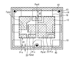
- FIG. 3A is a top view showing the configuration of the wiring board in the first embodiment
- FIG. 3B is a view of the lower surface of the wiring board seen through from above.
- FIG. 4 is a top view showing the configuration of the wiring board in the comparative example.
- FIG. 5 is a diagram illustrating the isolation characteristics of the duplexers according to the first embodiment and the comparative example.
- FIG. 6 is a top view showing the configuration of the wiring board according to the second embodiment of the present invention.
- FIG. 7 is a top view showing the configuration of the wiring board according to the third embodiment of the present invention.
- FIG. 8 is a top view showing the configuration of the wiring board according to the fourth embodiment of the present invention.
- FIG. 1 is a functional block diagram illustrating a configuration of a duplexer.
- a reception filter 50 is connected between the reception terminal Trx and the antenna terminal Tant.
- a transmission filter 52 is connected between the transmission terminal Ttx and the antenna terminal Tant.
- a matching circuit 54 is disposed between the antenna terminal Tant and at least one of the reception filter 50 and the transmission filter 52.
- the reception filter 50 filters the reception signal input to the antenna terminal Tant and outputs it to the reception terminal Trx.
- the reception filter 50 suppresses the transmission signal from being output to the reception terminal Trx by suppressing the transmission signal.
- the transmission filter 52 filters the transmission signal input to the transmission terminal Ttx and outputs it to the antenna terminal Tant.
- the transmission filter 52 suppresses the reception signal from being output to the transmission terminal Ttx by suppressing the reception signal.
- the reception signal and the transmission signal have different frequency bands, and the reception filter 50 and the transmission filter 52 have different pass bands.
- the matching circuit 54 matches the impedance between the antenna terminal Tant and the reception filter 50 and the transmission filter 52.
- the transmission-reception isolation characteristic indicates the degree of signal leakage from the transmission terminal Ttx to the reception terminal Trx. When the transmission-reception isolation characteristics deteriorate, the transmission signal tends to leak from the transmission terminal Ttx to the reception terminal Trx.
- FIG. 2 shows a cross-sectional structure of the duplexer according to the first embodiment of the present invention.
- the cross section corresponds to the XX cross section in FIG.
- the duplexer 100 includes a wiring substrate 10, a reception filter chip 20, a transmission filter chip 22, and a metal sealing portion 26.
- the wiring substrate 10 is made of a ceramic material or resin material mainly composed of two layers of aluminum oxide, and metal layers are selectively disposed on the upper surface, the interlayer, and the lower surface.
- an annular metal layer 14 is provided so as to be surrounded.
- a wiring metal layer 16 is selectively disposed between the insulating layer 10b and the lower insulating layer 10a, that is, between the layers, and an external connection electrode is provided on the surface (lower surface) of the lower insulating layer 10a. Terminals (foot pads) 18 are selectively provided.
- an interlayer connection conductor (not shown) selectively disposed in the insulating layers 10a and 10b. ).
- the annular metal layer 14 is connected to the external connection electrode terminal 18 which is set to the ground potential.
- the electrode terminal 12, the annular metal layer 14, and the wiring metal layer 16 are formed of copper (Cu), silver (Ag), gold (Au), or the like.
- the reception filter chip 20 and the transmission filter chip 22 are flip-chip mounted on the upper surface of the wiring substrate 10 via bumps 24 made of copper.
- the active region (filter forming surface) of the filter chip is disposed to face the upper surface of the wiring substrate 10.
- the reception filter chip 20 and the transmission filter chip 22 are surrounded by a metal sealing part 26.
- the metal sealing portion 26 is made of tin (Sn) -silver (Ag) -copper (Cu) solder, its inner side surface is in contact with the side surface of the filter chip, and its lower surface is in contact with the annular metal layer 14. .
- a cap plate 28 made of Kovar is disposed on the reception filter chip 20, the transmission filter chip 22 and the metal sealing portion 26.
- reception filter chip 20 and the transmission filter chip 22 are received in the cavity 29 formed by the cap plate 28 and the metal sealing portion 26 and are sealed by the wiring board 10.
- the metal sealing portion 26 and the cap plate 28 are covered with a protective film 30 made of nickel (Ni), and the protective film 30 is also in contact with the annular metal layer 14.
- cap plate 28 and the protective film 30 it is possible to prevent the metal sealing portion 26 from being deformed due to heat applied when the duplexer 100 is mounted on an electronic device mounting board or the like. -It can also be suppressed.
- solder As a material constituting the bump 24, gold or solder can be used in addition to copper.
- solder or metal other than the above-described tin-silver-copper can be used.
- the cap plate 28 and the protective film 30 may be made of an insulator other than the metal as described above.
- the melting points of the cap plate 28 and the protective film 30 are preferably higher than the melting point of the metal sealing portion 26.
- the wiring board 10 has a single layer structure or three or more layers as required.
- FIG. 3A shows the upper surface of the wiring board 10 in the duplexer 100 according to the first embodiment
- FIG. 3B shows a state where the lower surface of the wiring board 10 is seen through from above.
- FIG. 3A the external shapes of the reception filter chip 20 and the transmission filter chip 22 to be mounted are shown as rectangles drawn by thick broken lines.
- An antenna electrode Pant, a reception electrode Prx, a transmission electrode Ptx, and a ground electrode Pgnd are formed with electrode terminals 12 on the upper surface of the wiring substrate 10 located immediately below the reception filter chip 20 and the transmission filter chip 22, respectively. ing.
- the antenna electrode, the reception electrode, and the ground electrode in the reception filter chip 20 are connected to the antenna electrode Pant, the reception electrode Prx, and the ground electrode Pgnd through bumps 24 (see FIG. 2).
- the antenna electrode, the transmission electrode, and the ground electrode in the transmission filter chip 22 are connected to the antenna electrode Pant, the transmission electrode Ptx, and the ground electrode Pgnd via the bump 24.
- the antenna electrode Pant, the reception electrode Prx, the transmission electrode Ptx, and the ground electrode Pgnd function as signal lines for propagating signals and the like, and for mounting and fixing when the reception filter chip 20 and the transmission filter chip 22 are flip-chipped. Functions as a pad.
- the annular metal layer 14 is disposed along the peripheral edge with a predetermined width, and a plurality of electrode terminals such as the antenna electrode Pant, the reception electrode Prx, the transmission electrode Ptx, and the ground electrode Pgnd. 12 is surrounded.
- the electrode terminals 18 arranged on the lower surface of the wiring board 10 are indicated by thin broken lines.
- a transmission foot pad Ftx that functions as a transmission terminal Ttx
- a reception foot pad Frx that functions as a reception terminal Trx
- an antenna that functions as an antenna terminal Fant.
- a foot pad Fant and a ground foot pad Fgnd functioning as a ground terminal are formed with electrode terminals 18 respectively.
- the transmission foot pad Ftx, the reception foot pad Frx, the antenna foot pad Fant, and the ground foot pad Fgnd correspond to the transmission electrode Ptx and the reception electrode corresponding to each other through the wiring metal layer 16 and the interlayer connection conductor (via) 15 of the wiring substrate 10. It is electrically connected to Prx, antenna electrode Pant, or ground electrode Pgnd.
- the annular metal layer 14 is electrically connected to the ground foot pad Fgnd through the interlayer connection conductor 15.
- a side of the annular metal layer 14 closest to the reception foot pad Frx and the transmission foot pad Ftx is a first side 40, and a side opposite to the first side 40 is a second side 42.
- the width of the first side 40 is the width W1
- the shortest distance between the first side 40 and the receiving electrode Prx is the distance d1
- the shortest distance between the second side 42 and the antenna electrode Pant is the distance d2.
- the reception filter 50 is configured with a ladder type filter using a piezoelectric thin film resonator
- the transmission filter 52 is configured with a ladder type filter using a surface acoustic wave resonator.
- the chip size Lr1 ⁇ Lr2 of the reception filter chip 20 was 1.0 mm ⁇ 0.79 mm, and the chip size Lt1 ⁇ Lt2 of the transmission filter chip 22 was 1.0 mm ⁇ 0.79 mm.
- the outer dimensions L1 ⁇ L2 of the wiring board 10 were set to 2.0 mm ⁇ 2.5 mm. Furthermore, the film thicknesses of the first insulating layer 10a and the second insulating layer 10b were each 0.089 mm.
- the width W1 of the annular metal layer 14 was set to 0.15 mm, and the distance d1 and the distance d2 were set to 0.40 mm and 0.30 mm, respectively.
- the width W1 of the annular metal layer 14 was 0.47 mm, and the distance d1 and the distance d2 were 0.08 mm and 0.15 mm, respectively.
- the chip size Lr1 ⁇ Lr2 of the reception filter chip 20, the chip size Lt1 ⁇ Lt2 of the transmission filter chip 22, the size L1 ⁇ L2 of the wiring substrate 10, and the film thicknesses of the insulating layers 10a and 10b were the same as those in the first embodiment. Other configurations are the same as those in the first embodiment, and the description thereof is omitted.
- the transmission-reception isolation characteristics of the duplexers according to Example 1 and the comparative example were measured.
- the transmission band was selected from 1850 MHz to 1910 MHz, and the reception band was selected from 1930 MHz to 1990 MHz.
- FIG. 5 shows the isolation characteristics of the duplexer in Example 1 and the duplexer in the comparative example.
- the duplexer in the first embodiment of the present invention has an increased attenuation in the transmission band as compared with the comparative example, and the transmission-reception isolation characteristics are clearly improved.
- the transmission foot pad Ftx and the annular metal layer 14 are electromagnetically coupled as a cause of deterioration of the transmission-reception isolation characteristics, and the annular metal layer 14 and the reception electrode Prx are As a result of electromagnetic coupling, a signal may leak from the transmission foot pad Ftx to the reception electrode Prx.
- the shortest distance d1 between the first side 40 of the annular metal layer 14 and the receiving electrode Prx is larger than the width W1. Furthermore, the distance d1 is more preferably 1.5 times or more of the width W1, and the distance d1 is more preferably twice or more of the width W1.
- the reception pad and the antenna pad are provided apart from each other in order to suppress interference between the two pads. For this reason, the reception pad and the antenna pad are provided on the diagonal line of the reception filter chip 20.
- the distance between the antenna electrode Pant and the annular metal layer 14 becomes closer if the distance between the reception electrode Prx and the annular metal layer 14 is increased. End up.
- the shortest distance d1 between the first side 40 of the annular metal layer 14 and the receiving electrode Prx is greater than the shortest distance d2 between the second side 42 of the annular metal layer 14 and the antenna electrode Pant. Is also preferably large. Furthermore, the distance d1 is more preferably 1.5 times or more than the distance d2, and the distance d1 is more preferably twice or more than the distance d2.
- the metal sealing portion 26 when the metal sealing portion 26 is in contact with the annular metal layer 14 and seals the reception filter and the transmission filter, the volume of the annular metal is increased. The transmission signal leaks through the unit 26 increases.
- the wiring board 10 has a quadrangular (rectangular) planar shape.
- the reception foot pad Frx and the transmission foot pad Ftx are connected to the first metal ring 14 in the first shape.
- the antenna foot pad Fant is disposed in the center of the second side 42 facing the first side 40.
- the reception filter chip 20 and the transmission filter chip 22 may be mounted face-up on the wiring board 10. However, in order to reduce the size of the duplexer, it is preferable that the reception filter chip 20 and the transmission filter chip 22 are flip-chip mounted on the wiring substrate 10.
- a filter using a surface acoustic wave resonator or a piezoelectric thin film resonator can be used.
- ladder type filters or multimode filters can be used as the reception filter 50 and the transmission filter 52.
- the annular metal layer 14 may surround at least a part of the antenna electrode Pant, the reception electrode Prx, the transmission electrode Ptx, and the ground electrode Pgnd. However, in order to hermetically seal the reception filter chip 20 and the transmission filter chip 22 using the metal sealing portion 26, the annular metal layer 14 includes the antenna electrode Pant, the reception electrode Prx, the transmission electrode Ptx, and the ground electrode Pgnd. Preferably it is completely enclosed.
- the annular metal layer 14 is electrically connected to the ground foot pad Fgnd via at least one interlayer connection conductor 15.
- FIG. 6 shows a top view of the wiring board 10 in Example 2 of the present invention.
- the chip size of the transmission filter chip 22 is larger than that of the first embodiment shown in FIG.
- the distance d2 is larger than the shortest distance d3 between the first side 40 and the transmission electrode Ptx.
- Other configurations are the same as those in the first embodiment, and a description thereof will be omitted.
- the transmission signal leaking to the annular metal layer 14 does not greatly depend on the shortest distance d3 between the transmission electrode Ptx and the first side 40 of the annular metal layer 14.
- the power of the transmission signal leaking to the annular metal layer 14 is small, the signal leaking to the reception electrode Prx via the annular metal layer 14 depends on the distance d1.
- the shortest distance d1 between the first side 40 of the annular metal layer 14 and the reception electrode Prx is preferably larger than the shortest distance d3 between the first side 40 and the transmission electrode Ptx. Furthermore, the distance d1 is more preferably 1.5 times or more than d3, and the distance d1 is more preferably twice or more than the distance d3.
- the reception filter chip 20 is smaller in size than the transmission filter chip 22.
- the distance d1 can be made larger than the distance d3.
- FIG. 7 shows a top view of the wiring board 10 in Example 3 of the present invention.
- two receiving electrodes Prx are provided.
- a balanced signal is propagated to the two receiving electrodes Prx.
- the width W1 is the width of the first side 40
- the distance d1 is the shortest distance between the first side 40 and the receiving electrode Prx
- the distance d2 is the shortest distance between the second side 42 and the antenna electrode Pant.
- Other configurations are the same as those of the first embodiment, and the description thereof is omitted.
- the balance characteristic can also be improved.
- the received signal may be an unbalanced signal.
- the transmission signal may be either a balanced signal or an unbalanced signal.
- FIG. 8 shows a top view of the wiring board 10 in Example 4 of the present invention.
- the reception filter and the transmission filter are formed in one filter chip 23.
- the width W1 is the width of the first side 40
- the distance d1 is the shortest distance between the first side 40 and the reception electrode Prx
- the distance d2 is the shortest distance between the second side 42 and the antenna electrode Pant.
- Other configurations are the same as those in the first embodiment, and a description thereof will be omitted.
- the reception filter 50 and the transmission filter 52 may be formed in one filter chip 23.
- the elements such as an inductor and / or a capacitor constituting the matching circuit 54 shown in FIG. These elements may be formed in the wiring board 10.
Landscapes
- Engineering & Computer Science (AREA)
- Computer Networks & Wireless Communication (AREA)
- Signal Processing (AREA)
- Surface Acoustic Wave Elements And Circuit Networks Thereof (AREA)
- Control Of Motors That Do Not Use Commutators (AREA)
- Transceivers (AREA)
- Piezo-Electric Or Mechanical Vibrators, Or Delay Or Filter Circuits (AREA)
Abstract
Description
尚、図3(a)にあっては、配線基板10の下面に配置された電極端子18を細い破線をもって示している。
さらに、距離d1がd3の1.5倍以上であることがより好ましく、距離d1が距離d3の2倍以上であることがより好ましい。
12 電極端子
14 環状金属層
15 層間接続用導体(ビア)
16 配線金属層
18 外部接続用電極端子
20 受信フィルタチップ
22 送信フィルタチップ
24 バンプ
26 金属封止部
28 キャップ板
30 保護膜
40 第1の辺
42 第2の辺
Claims (7)
- 受信端子とアンテナ端子との間に接続された受信フィルタと、
送信端子と前記アンテナ端子との間に接続された送信フィルタと、
前記受信端子、前記送信端子および前記アンテナ端子が下面に形成され、前記受信端子と電気的に接続する受信電極と、前記送信端子と電気的に接続する送信電極と、前記アンテナ端子と電気的に接続するアンテナ電極と、前記受信電極、前記送信電極および前記アンテナ電極を囲みグランドに電気的に接続された環状金属層とが上面に形成され、前記受信フィルタと前記送信フィルタとを前記上面に搭載する配線基板とを具備し、
前記受信端子および前記送信端子に最も近い前記環状金属層の辺と前記受信電極との最短距離が、前記環状金属層の前記辺の幅より大きいことを特徴とするデュープレクサ。 - 前記環状金属層に接触し、前記受信フィルタおよび前記送信フィルタを封止する金属封止部を具備することを特徴とする請求項1記載のデュープレクサ。
- 前記環状金属層の前記辺と前記受信電極との最短距離が、前記環状金属層の前記辺と前記送信電極との最短距離より大きいことを特徴とする請求項1または2記載のデュープレクサ。
- 前記環状金属層の前記辺と前記受信電極との最短距離が、前記環状金属層と前記アンテナ電極との最短距離より大きいことを特徴とする請求項1から3のいずれか一項記載のデュープレクサ。
- 前記配線基板は四角形状を有し、
前記受信端子と前記送信端子は、前記環状金属層の前記辺の両端に形成され、
前記アンテナ端子は、前記環状金属層の前記辺に対向する辺の中央部に形成されていることを特徴とする請求項1から4のいずれか一項記載のデュープレクサ。 - 前記配線基板は平板状であることを特徴とする請求項1から5のいずれか一項記載のデュープレクサ。
- 前記受信フィルタおよび前記送信フィルタは、前記配線基板にフリップチップ実装されていることを特徴とする請求項1から6のいずれか一項記載のデュープレクサ。
Priority Applications (4)
| Application Number | Priority Date | Filing Date | Title |
|---|---|---|---|
| CN201180030472.6A CN102959795B (zh) | 2011-04-20 | 2011-04-20 | 双工器 |
| JP2012542058A JP5740410B2 (ja) | 2011-04-20 | 2011-04-20 | デュープレクサ |
| PCT/JP2011/059745 WO2012144036A1 (ja) | 2011-04-20 | 2011-04-20 | デュープレクサ |
| US13/610,399 US9070963B2 (en) | 2011-04-20 | 2012-09-11 | Duplexer |
Applications Claiming Priority (1)
| Application Number | Priority Date | Filing Date | Title |
|---|---|---|---|
| PCT/JP2011/059745 WO2012144036A1 (ja) | 2011-04-20 | 2011-04-20 | デュープレクサ |
Related Child Applications (1)
| Application Number | Title | Priority Date | Filing Date |
|---|---|---|---|
| US13/610,399 Continuation US9070963B2 (en) | 2011-04-20 | 2012-09-11 | Duplexer |
Publications (1)
| Publication Number | Publication Date |
|---|---|
| WO2012144036A1 true WO2012144036A1 (ja) | 2012-10-26 |
Family
ID=47041186
Family Applications (1)
| Application Number | Title | Priority Date | Filing Date |
|---|---|---|---|
| PCT/JP2011/059745 Ceased WO2012144036A1 (ja) | 2011-04-20 | 2011-04-20 | デュープレクサ |
Country Status (4)
| Country | Link |
|---|---|
| US (1) | US9070963B2 (ja) |
| JP (1) | JP5740410B2 (ja) |
| CN (1) | CN102959795B (ja) |
| WO (1) | WO2012144036A1 (ja) |
Cited By (5)
| Publication number | Priority date | Publication date | Assignee | Title |
|---|---|---|---|---|
| JP2015002381A (ja) * | 2013-06-13 | 2015-01-05 | 太陽誘電株式会社 | 弾性波デバイス |
| JP2015061233A (ja) * | 2013-09-19 | 2015-03-30 | 株式会社村田製作所 | 分波器 |
| JP2015204531A (ja) * | 2014-04-14 | 2015-11-16 | 太陽誘電株式会社 | 電子デバイス及びその製造方法 |
| US10693440B2 (en) | 2017-06-13 | 2020-06-23 | Taiyo Yuden Co., Ltd. | Acoustic wave device |
| JP2022054986A (ja) * | 2020-09-28 | 2022-04-07 | 太陽誘電株式会社 | マルチプレクサ |
Families Citing this family (4)
| Publication number | Priority date | Publication date | Assignee | Title |
|---|---|---|---|---|
| WO2011136100A1 (ja) * | 2010-04-30 | 2011-11-03 | 株式会社村田製作所 | 複合部品 |
| CN105814796B (zh) * | 2013-12-25 | 2019-04-19 | 株式会社村田制作所 | 弹性波滤波器设备 |
| CN104885293B (zh) * | 2013-12-30 | 2018-05-29 | 华为技术有限公司 | 谐振器、滤波器、双工器、多工器及通信设备 |
| CN115882819A (zh) * | 2021-09-28 | 2023-03-31 | 诺思(天津)微系统有限责任公司 | 双工器装置、多工器及通信设备 |
Citations (5)
| Publication number | Priority date | Publication date | Assignee | Title |
|---|---|---|---|---|
| JP2003204245A (ja) * | 2002-01-08 | 2003-07-18 | Murata Mfg Co Ltd | 弾性表面波装置、分波器 |
| JP2005159896A (ja) * | 2003-11-27 | 2005-06-16 | Sanyo Electric Co Ltd | アンテナ共用器 |
| JP2006014296A (ja) * | 2004-05-27 | 2006-01-12 | Kyocera Corp | 弾性表面波装置及び通信機器 |
| JP2006203149A (ja) * | 2004-12-24 | 2006-08-03 | Fujitsu Media Device Kk | 電子部品及びその製造方法 |
| JP2007258832A (ja) * | 2006-03-20 | 2007-10-04 | Kyocera Corp | 弾性表面波素子、弾性表面波装置、弾性表面波装置の製造方法、通信装置、送信装置および受信装置 |
Family Cites Families (5)
| Publication number | Priority date | Publication date | Assignee | Title |
|---|---|---|---|---|
| US4499440A (en) * | 1983-08-22 | 1985-02-12 | United Technologies Corporation | Low reflectivity electrodes in semiconductive SAW devices |
| US7298231B2 (en) | 2004-05-27 | 2007-11-20 | Kyocera Corporation | Surface acoustic wave device and communication apparatus |
| JP4637669B2 (ja) * | 2005-07-13 | 2011-02-23 | 京セラ株式会社 | フィルタ装置とこれを用いたマルチバンドフィルタ、分波器及び通信装置 |
| JP5079813B2 (ja) * | 2007-08-30 | 2012-11-21 | 京セラ株式会社 | 電子部品 |
| JP5686943B2 (ja) | 2008-09-17 | 2015-03-18 | 太陽誘電株式会社 | 弾性波デバイス及びその製造方法 |
-
2011
- 2011-04-20 CN CN201180030472.6A patent/CN102959795B/zh active Active
- 2011-04-20 WO PCT/JP2011/059745 patent/WO2012144036A1/ja not_active Ceased
- 2011-04-20 JP JP2012542058A patent/JP5740410B2/ja active Active
-
2012
- 2012-09-11 US US13/610,399 patent/US9070963B2/en active Active
Patent Citations (5)
| Publication number | Priority date | Publication date | Assignee | Title |
|---|---|---|---|---|
| JP2003204245A (ja) * | 2002-01-08 | 2003-07-18 | Murata Mfg Co Ltd | 弾性表面波装置、分波器 |
| JP2005159896A (ja) * | 2003-11-27 | 2005-06-16 | Sanyo Electric Co Ltd | アンテナ共用器 |
| JP2006014296A (ja) * | 2004-05-27 | 2006-01-12 | Kyocera Corp | 弾性表面波装置及び通信機器 |
| JP2006203149A (ja) * | 2004-12-24 | 2006-08-03 | Fujitsu Media Device Kk | 電子部品及びその製造方法 |
| JP2007258832A (ja) * | 2006-03-20 | 2007-10-04 | Kyocera Corp | 弾性表面波素子、弾性表面波装置、弾性表面波装置の製造方法、通信装置、送信装置および受信装置 |
Cited By (6)
| Publication number | Priority date | Publication date | Assignee | Title |
|---|---|---|---|---|
| JP2015002381A (ja) * | 2013-06-13 | 2015-01-05 | 太陽誘電株式会社 | 弾性波デバイス |
| JP2015061233A (ja) * | 2013-09-19 | 2015-03-30 | 株式会社村田製作所 | 分波器 |
| JP2015204531A (ja) * | 2014-04-14 | 2015-11-16 | 太陽誘電株式会社 | 電子デバイス及びその製造方法 |
| US10693440B2 (en) | 2017-06-13 | 2020-06-23 | Taiyo Yuden Co., Ltd. | Acoustic wave device |
| JP2022054986A (ja) * | 2020-09-28 | 2022-04-07 | 太陽誘電株式会社 | マルチプレクサ |
| JP7606306B2 (ja) | 2020-09-28 | 2024-12-25 | 太陽誘電株式会社 | マルチプレクサ |
Also Published As
| Publication number | Publication date |
|---|---|
| CN102959795B (zh) | 2016-08-03 |
| JP5740410B2 (ja) | 2015-06-24 |
| US20130002371A1 (en) | 2013-01-03 |
| JPWO2012144036A1 (ja) | 2014-07-28 |
| US9070963B2 (en) | 2015-06-30 |
| CN102959795A (zh) | 2013-03-06 |
Similar Documents
| Publication | Publication Date | Title |
|---|---|---|
| JP5740410B2 (ja) | デュープレクサ | |
| US9887686B2 (en) | Acoustic wave device, transceiver device, and mobile communication device | |
| JP5144379B2 (ja) | 分波器 | |
| KR100712441B1 (ko) | 탄성표면파 장치 및 통신기기 | |
| US20200211998A1 (en) | Radio-frequency module and communication device | |
| JP6809994B2 (ja) | 電子フィルタとフィルタデバイス | |
| JP6282410B2 (ja) | モジュール | |
| JP2007110202A (ja) | 複合フィルタチップ | |
| JP2003198325A (ja) | 分波器、通信装置 | |
| US20130043961A1 (en) | Duplexer with shielding bondwires between filters | |
| US8766744B2 (en) | Duplexer and electronic device having the same | |
| JP5583612B2 (ja) | 分波器 | |
| JP2005268878A (ja) | アンテナ共用器 | |
| CN102571030B (zh) | 双工器 | |
| US20240292519A1 (en) | High frequency module and communication device | |
| KR20030081419A (ko) | 탄성 표면파 장치 | |
| JP6253306B2 (ja) | 電子デバイス | |
| JP2005102114A (ja) | 弾性表面波装置、電子装置および通信装置 | |
| JP4969193B2 (ja) | 分波器 | |
| JP2025129974A (ja) | 高周波モジュール、及び、通信装置 | |
| WO2022138441A1 (ja) | 高周波モジュール及び通信装置 | |
| JP2004207871A (ja) | 弾性表面波フィルタ用パッケージ | |
| JP2002100956A (ja) | 弾性表面波フィルタ |
Legal Events
| Date | Code | Title | Description |
|---|---|---|---|
| WWE | Wipo information: entry into national phase |
Ref document number: 201180030472.6 Country of ref document: CN |
|
| ENP | Entry into the national phase |
Ref document number: 2012542058 Country of ref document: JP Kind code of ref document: A |
|
| 121 | Ep: the epo has been informed by wipo that ep was designated in this application |
Ref document number: 11863853 Country of ref document: EP Kind code of ref document: A1 |
|
| NENP | Non-entry into the national phase |
Ref country code: DE |
|
| 122 | Ep: pct application non-entry in european phase |
Ref document number: 11863853 Country of ref document: EP Kind code of ref document: A1 |