WO2012141066A1 - 酸化物型半導体材料及びスパッタリングターゲット - Google Patents
酸化物型半導体材料及びスパッタリングターゲット Download PDFInfo
- Publication number
- WO2012141066A1 WO2012141066A1 PCT/JP2012/059329 JP2012059329W WO2012141066A1 WO 2012141066 A1 WO2012141066 A1 WO 2012141066A1 JP 2012059329 W JP2012059329 W JP 2012059329W WO 2012141066 A1 WO2012141066 A1 WO 2012141066A1
- Authority
- WO
- WIPO (PCT)
- Prior art keywords
- dopant
- semiconductor material
- oxide
- oxide semiconductor
- tft
- Prior art date
- Legal status (The legal status is an assumption and is not a legal conclusion. Google has not performed a legal analysis and makes no representation as to the accuracy of the status listed.)
- Ceased
Links
Images


Classifications
-
- C—CHEMISTRY; METALLURGY
- C01—INORGANIC CHEMISTRY
- C01G—COMPOUNDS CONTAINING METALS NOT COVERED BY SUBCLASSES C01D OR C01F
- C01G19/00—Compounds of tin
-
- C—CHEMISTRY; METALLURGY
- C01—INORGANIC CHEMISTRY
- C01G—COMPOUNDS CONTAINING METALS NOT COVERED BY SUBCLASSES C01D OR C01F
- C01G19/00—Compounds of tin
- C01G19/006—Compounds containing tin, with or without oxygen or hydrogen, and containing two or more other elements
-
- C—CHEMISTRY; METALLURGY
- C23—COATING METALLIC MATERIAL; COATING MATERIAL WITH METALLIC MATERIAL; CHEMICAL SURFACE TREATMENT; DIFFUSION TREATMENT OF METALLIC MATERIAL; COATING BY VACUUM EVAPORATION, BY SPUTTERING, BY ION IMPLANTATION OR BY CHEMICAL VAPOUR DEPOSITION, IN GENERAL; INHIBITING CORROSION OF METALLIC MATERIAL OR INCRUSTATION IN GENERAL
- C23C—COATING METALLIC MATERIAL; COATING MATERIAL WITH METALLIC MATERIAL; SURFACE TREATMENT OF METALLIC MATERIAL BY DIFFUSION INTO THE SURFACE, BY CHEMICAL CONVERSION OR SUBSTITUTION; COATING BY VACUUM EVAPORATION, BY SPUTTERING, BY ION IMPLANTATION OR BY CHEMICAL VAPOUR DEPOSITION, IN GENERAL
- C23C14/00—Coating by vacuum evaporation, by sputtering or by ion implantation of the coating forming material
- C23C14/06—Coating by vacuum evaporation, by sputtering or by ion implantation of the coating forming material characterised by the coating material
- C23C14/08—Oxides
- C23C14/086—Oxides of zinc, germanium, cadmium, indium, tin, thallium or bismuth
-
- C—CHEMISTRY; METALLURGY
- C23—COATING METALLIC MATERIAL; COATING MATERIAL WITH METALLIC MATERIAL; CHEMICAL SURFACE TREATMENT; DIFFUSION TREATMENT OF METALLIC MATERIAL; COATING BY VACUUM EVAPORATION, BY SPUTTERING, BY ION IMPLANTATION OR BY CHEMICAL VAPOUR DEPOSITION, IN GENERAL; INHIBITING CORROSION OF METALLIC MATERIAL OR INCRUSTATION IN GENERAL
- C23C—COATING METALLIC MATERIAL; COATING MATERIAL WITH METALLIC MATERIAL; SURFACE TREATMENT OF METALLIC MATERIAL BY DIFFUSION INTO THE SURFACE, BY CHEMICAL CONVERSION OR SUBSTITUTION; COATING BY VACUUM EVAPORATION, BY SPUTTERING, BY ION IMPLANTATION OR BY CHEMICAL VAPOUR DEPOSITION, IN GENERAL
- C23C14/00—Coating by vacuum evaporation, by sputtering or by ion implantation of the coating forming material
- C23C14/22—Coating by vacuum evaporation, by sputtering or by ion implantation of the coating forming material characterised by the process of coating
- C23C14/34—Sputtering
- C23C14/3407—Cathode assembly for sputtering apparatus, e.g. Target
- C23C14/3414—Metallurgical or chemical aspects of target preparation, e.g. casting, powder metallurgy
-
- H—ELECTRICITY
- H10—SEMICONDUCTOR DEVICES; ELECTRIC SOLID-STATE DEVICES NOT OTHERWISE PROVIDED FOR
- H10D—INORGANIC ELECTRIC SEMICONDUCTOR DEVICES
- H10D30/00—Field-effect transistors [FET]
- H10D30/60—Insulated-gate field-effect transistors [IGFET]
- H10D30/67—Thin-film transistors [TFT]
- H10D30/674—Thin-film transistors [TFT] characterised by the active materials
- H10D30/6755—Oxide semiconductors, e.g. zinc oxide, copper aluminium oxide or cadmium stannate
-
- H—ELECTRICITY
- H10—SEMICONDUCTOR DEVICES; ELECTRIC SOLID-STATE DEVICES NOT OTHERWISE PROVIDED FOR
- H10D—INORGANIC ELECTRIC SEMICONDUCTOR DEVICES
- H10D62/00—Semiconductor bodies, or regions thereof, of devices having potential barriers
- H10D62/10—Shapes, relative sizes or dispositions of the regions of the semiconductor bodies; Shapes of the semiconductor bodies
-
- H—ELECTRICITY
- H10—SEMICONDUCTOR DEVICES; ELECTRIC SOLID-STATE DEVICES NOT OTHERWISE PROVIDED FOR
- H10P—GENERIC PROCESSES OR APPARATUS FOR THE MANUFACTURE OR TREATMENT OF DEVICES COVERED BY CLASS H10
- H10P14/00—Formation of materials, e.g. in the shape of layers or pillars
- H10P14/20—Formation of materials, e.g. in the shape of layers or pillars of semiconductor materials
- H10P14/22—Formation of materials, e.g. in the shape of layers or pillars of semiconductor materials using physical deposition, e.g. vacuum deposition or sputtering
-
- H—ELECTRICITY
- H10—SEMICONDUCTOR DEVICES; ELECTRIC SOLID-STATE DEVICES NOT OTHERWISE PROVIDED FOR
- H10P—GENERIC PROCESSES OR APPARATUS FOR THE MANUFACTURE OR TREATMENT OF DEVICES COVERED BY CLASS H10
- H10P14/00—Formation of materials, e.g. in the shape of layers or pillars
- H10P14/20—Formation of materials, e.g. in the shape of layers or pillars of semiconductor materials
- H10P14/34—Deposited materials, e.g. layers
- H10P14/3402—Deposited materials, e.g. layers characterised by the chemical composition
- H10P14/3424—Deposited materials, e.g. layers characterised by the chemical composition being Group IIB-VIA materials
- H10P14/3426—Oxides
-
- H—ELECTRICITY
- H10—SEMICONDUCTOR DEVICES; ELECTRIC SOLID-STATE DEVICES NOT OTHERWISE PROVIDED FOR
- H10P—GENERIC PROCESSES OR APPARATUS FOR THE MANUFACTURE OR TREATMENT OF DEVICES COVERED BY CLASS H10
- H10P14/00—Formation of materials, e.g. in the shape of layers or pillars
- H10P14/20—Formation of materials, e.g. in the shape of layers or pillars of semiconductor materials
- H10P14/34—Deposited materials, e.g. layers
- H10P14/3402—Deposited materials, e.g. layers characterised by the chemical composition
- H10P14/3434—Deposited materials, e.g. layers characterised by the chemical composition being oxide semiconductor materials
-
- H—ELECTRICITY
- H10—SEMICONDUCTOR DEVICES; ELECTRIC SOLID-STATE DEVICES NOT OTHERWISE PROVIDED FOR
- H10P—GENERIC PROCESSES OR APPARATUS FOR THE MANUFACTURE OR TREATMENT OF DEVICES COVERED BY CLASS H10
- H10P14/00—Formation of materials, e.g. in the shape of layers or pillars
- H10P14/20—Formation of materials, e.g. in the shape of layers or pillars of semiconductor materials
- H10P14/34—Deposited materials, e.g. layers
- H10P14/3438—Doping during depositing
- H10P14/3441—Conductivity type
- H10P14/3446—Transition metal elements; Rare earth elements
-
- C—CHEMISTRY; METALLURGY
- C01—INORGANIC CHEMISTRY
- C01P—INDEXING SCHEME RELATING TO STRUCTURAL AND PHYSICAL ASPECTS OF SOLID INORGANIC COMPOUNDS
- C01P2002/00—Crystal-structural characteristics
- C01P2002/50—Solid solutions
- C01P2002/52—Solid solutions containing elements as dopants
-
- C—CHEMISTRY; METALLURGY
- C01—INORGANIC CHEMISTRY
- C01P—INDEXING SCHEME RELATING TO STRUCTURAL AND PHYSICAL ASPECTS OF SOLID INORGANIC COMPOUNDS
- C01P2006/00—Physical properties of inorganic compounds
- C01P2006/40—Electric properties
Definitions
- the present invention relates to a semiconductor material for forming a semiconductor element constituting a display device such as a liquid crystal display, and more particularly to an oxide semiconductor material containing Zn oxide and Sn oxide.
- TFT thin film transistor
- an oxide semiconductor material is used as a constituent material thereof.
- this oxide semiconductor material attention is paid to IGZO (In—Ga—Zn—O-based oxide) which is a kind of transparent oxide semiconductor material (see Patent Document 1).
- This IGZO has the highest carrier mobility next to polycrystalline Si (silicon), which has been used in the past, and has little variation in TFT characteristics like a-Si (amorphous silicon), so it is promising as a future semiconductor material. It is beginning to be widely used as a product.
- a change in the display method has occurred.
- a liquid crystal display capable of stereoscopic display (3D) in addition to planar display (2D) is provided.
- This stereoscopic display (3D) type liquid crystal display is realized by making it possible to see different images on the left and right of the display screen by control using a switch liquid crystal. Therefore, for such a stereoscopic display type liquid crystal display, a switching element capable of realizing a higher response speed is required.
- IGZO oxide semiconductor materials
- a TFT having a high response speed has high carrier mobility.
- IGZO is 1 to 2 orders of magnitude larger than a-Si, and its carrier mobility is about 5 to 10 cm 2 / Vs. Therefore, with this IGZO, it can be used as a constituent material of a TFT that is a switching element of a stereoscopic display type liquid crystal display, but in order to realize a higher spec liquid crystal display, a TFT capable of realizing a higher response speed.
- constituent materials There are demands for constituent materials.
- this IGZO requires an annealing process of 350 ° C. or higher when forming a TFT, so it should be used for display devices that cannot be subjected to high-temperature heat treatment such as organic EL panels and electronic paper using a flexible substrate. It is pointed out that this is difficult.
- oxide-type semiconductor materials that do not use In or Ga have been demanded due to resource problems and effects on the human body and the environment, and development of alternative materials for IGZO from this point is also required.
- IGZO As an alternative material for IGZO, for example, an oxide semiconductor material (ZTO: Zn—Sn—O-based oxide) composed of Zn oxide and Sn oxide has been proposed (Patent Document 2, Patent Document 3). Patent Document 4). These prior art ZTOs have been developed to achieve high carrier mobility, but the heat treatment temperature at the time of TFT formation has not been studied, and their applicability to organic EL panels and electronic paper has been found. Absent. Therefore, the current situation is that further improvement is required for ZTO as an alternative material for IGZO.
- ZTO oxide semiconductor material
- Patent Document 3 Patent Document 3
- Patent Document 4 Patent Document 4
- the present invention has been made in the background as described above.
- the carrier mobility is equal to or higher than that of IGZO, and has a high carrier mobility of about 10 cm 2 / Vs, and 300
- An object of the present invention is to provide an oxide semiconductor material (ZTO: Zn—Sn—O-based oxide) composed of Zn oxide and Sn oxide, which does not require high-temperature heat treatment at a temperature of 0 ° C. or higher.
- the present inventors have studied various dopants to be included in an oxide semiconductor material containing Zn oxide and Sn oxide.
- a specific element is used as a dopant, high carrier mobility is achieved. It has been found that the ZTO film can be manufactured without the need for high-temperature heat treatment while maintaining the degree.
- the present invention is an oxide semiconductor material containing Zn oxide and Sn oxide, and as a dopant, any one or more of Mg (magnesium), Ca (calcium), La (lanthanum), and Y (yttrium)
- the dopant content is characterized in that the atomic ratio of the dopant with respect to the total number of atoms of Zn (zinc), Sn (tin) as a metal element is 0.09 or less.
- the carrier mobility is equal to or higher than that of IGZO, and carrier mobility of about 10 cm 2 / Vs can be realized. Can be formed. Moreover, since In and Ga are not included, there are no resource problems and the influence on the human body and the environment is reduced.
- the dopant of the oxide semiconductor material of the present invention can be any one of Mg, Ca, La, and Y, or a combination thereof.
- the dopant content is such that the atomic ratio of the dopant to the total number of atoms of Zn, Sn, and dopant as the metal elements is 0.09 or less.
- the dopant is included so that z / (x + y + z) ⁇ 0.09, where x is the number of Zn atoms as the metal element, y is the number of Sn atoms, and z is the number of dopant atoms. .
- this atomic ratio exceeds 0.09, the resistance value of the oxide semiconductor material increases, and semiconductor characteristics cannot be obtained.
- the carrier density is less than 1 ⁇ 10 18 cm ⁇ 3 , so that a carrier density equal to or lower than that of the IGZO film after heat treatment at 350 ° C. can be realized.
- the lower limit of the dopant content is not limited as long as a carrier density equal to or lower than that of IGZO can be realized and a switching element such as a TFT can be formed by heat treatment at 250 ° C. or lower.
- a switching element such as a TFT
- dopant content is less than 0.01 by atomic ratio. If it is less than 0.01, good TFT characteristics can be easily realized. Furthermore, when the dopant is Ca, the dopant content is less than 0.074 in atomic ratio, when the dopant is La, the dopant content is less than 0.027 in atomic ratio, and when the dopant is Y, the dopant content. Is preferably less than 0.038 in atomic ratio. Regarding the patterning characteristics when forming the element, it was confirmed that the one using Mg as a dopant was superior to the non-doped ZTO film.
- the ratio A / (A + B) is less than 0.4, the Sn ratio increases. Therefore, when the thin film formed during element formation is patterned by etching, the etching rate with an oxalic acid-based etching solution is extremely high. Slow down and not suitable for production process.
- the ratio exceeds 0.8, the ratio of Zn increases, so the resistance of the oxide semiconductor material to water decreases, and in the patterning process of wiring and semiconductor layers generally used when forming TFT elements.
- the ZTO film itself is damaged by the influence of the resist stripping solution and pure water cleaning, and the original TFT element characteristics cannot be realized. In some cases, the ZTO film is dissolved and dropped from the substrate, and the TFT element cannot be formed. .
- Zr can be further contained as a dopant. This is because Zr (zirconium) can also contribute to controlling the carrier mobility of the oxide semiconductor material of the present invention.
- the content of Zr is the total content of all dopants in the material. Is preferably 0.09 or less in atomic ratio.
- the Zr content is such that the atomic ratio of Zr to the total number of atoms of Zn (zinc), Sn (tin), and all the dopants constituting the oxide semiconductor material is 0.005 or less. It is preferable that
- the oxide semiconductor material of the present invention is very effective for a bottom gate type or top gate type thin film transistor.
- the oxide type semiconductor material of the present invention can realize carrier mobility equal to or higher than that of IGZO and can be used in low-temperature heat treatment at 250 ° C. or lower, so that a three-dimensional display type that requires a high response speed is required. It is suitable for a liquid crystal display, and can also be applied when forming a switching element such as an organic EL panel or electronic paper using a flexible substrate.
- the switching element is formed of the oxide semiconductor material of the present invention, it is effective to use a thin film formed of the oxide semiconductor material, and a sputtering method is used to form the thin film. Is preferred.
- An alloy target is preferred.
- a direct-current power source, a high-frequency power source, or a pulsed DC power source can be used for film formation by sputtering.
- a sputtering target containing at least one of Mg, Ca, La, and Y, and further containing a predetermined amount of Zr.
- Zn oxide, Sn oxide, and one or more kinds of oxides of Mg, Ca, La, and Y are formed so that an oxide semiconductor material having a target composition can be formed.
- a Zr oxide can be mixed and sintered.
- Zr can be further processed by mixing Zn oxide, Sn oxide, and one or more of Mg, Ca, La, and Y with a dry ball mill using a ZrO 2 ball as a medium. It can be included. Zr can be mixed as a dopant by such a dry ball mill. However, considering the uniformity of the oxide semiconductor material, it is preferable to mix Zr oxide.
- the film can be formed by the above sputtering method, but other film forming methods other than sputtering, such as pulsed laser deposition, can be applied. it can. Further, an element can be formed using the oxide semiconductor material of the present invention by applying a dispersion liquid in which nanoparticles of a semiconductor material are dispersed in a solvent or by forming a circuit by an ink jet method.
- oxide semiconductor material of the present invention carrier mobility equal to or higher than that of IGZO can be realized, and switching elements such as TFTs can be formed by low-temperature heat treatment at 250 ° C. or lower.
- switching elements such as TFTs can be formed by low-temperature heat treatment at 250 ° C. or lower.
- In and Ga are not included, there is no problem in terms of resources, and the influence on the human body and the environment can be reduced.
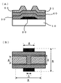
- TFT device schematic Measurement graph of TFT characteristics (Example 6, 200 ° C.) TFT characteristic measurement graph (Comparative Example 4, 200 ° C) Measurement graph of TFT characteristics (Example 5, 200 ° C.) Measurement graph of TFT characteristics (Example 12, 200 ° C.)
- Target preparation ZnO powder subjected to preliminary firing at 500 ° C. in air atmosphere, SnO 2 powder subjected to preliminary firing at 1050 ° C. in air atmosphere, and MgO powder not subjected to preliminary firing are weighed in predetermined amounts, respectively. It put into the resin pot (capacity 4L) and mixed with the ball mill. In this ball mill, mixing was performed at a rotation speed of 130 rpm and a mixing time of 12 hours. The mixed powder was sieved with a sieve having an opening of 500 ⁇ m and a wire diameter of 315 ⁇ m.
- the mixed powder under the sieve from which the coarse particles were removed was filled into a ⁇ 100 mm carbon press die, and a sintered body was produced by hot pressing.
- the hot press conditions were such that the Ar gas flow rate was 3 L / min, the temperature was raised to 1050 ° C. under a pressure of 9.4 MPa, held for 90 minutes under a pressure of 25 MPa, naturally cooled, and the sintered body was taken out.
- the sintered compact target formation for forming the thin film which becomes each atomic ratio shown in Table 1 with the above procedures was performed.
- Film formation was performed using a commercially available sheet-type sputtering apparatus (manufactured by Tokki Co., Ltd .: SML-464).
- the sputtering conditions were an ultimate vacuum of 1 ⁇ 10 ⁇ 5 Pa, an Ar / O 2 mixed gas as a sputtering gas, a sputtering gas pressure of 0.4 Pa, an oxygen partial pressure of 0.01 Pa, and room temperature (25 ° C.).
- a film having a thickness of about 100 nm was formed on a glass substrate (manufactured by Nippon Electric Glass Co., Ltd .: OA-10) by DC sputtering of 150 W.
- This film composition was formed by using an ICP (inductively coupled plasma) emission spectroscopic analyzer (manufactured by SII Nano Technology Co., Ltd .: Vista Pro).
- Table 1 shows the values of the atomic ratios of Zn / (Zn + Sn) and Mg / (Zn + Sn + Mg) calculated from the measured values of Zn, Sn, and Mg.
- TFT thin film transistor
- the composition of the oxide semiconductor material is such that the oxide semiconductor is cut while the element is cut and observed through a transmission electron microscope (TEM) or the like.
- TEM transmission electron microscope
- each sample formed was annealed at 200 ° C. and 300 ° C. for 1 hour in the air atmosphere, and the Hall effect measurement was performed to determine the specific resistance value, carrier mobility, and carrier density of each sample. .
- This Hall effect measurement was performed using each sample cut into a 10 mm ⁇ 10 mm square by a commercially available Hall effect measuring device (manufactured by Nanometrics Japan Co., Ltd .: HL5500PC). Table 1 shows the results of the specific resistance value, carrier mobility, and carrier density of each sample.
- FIG. 1 shows a schematic cross-sectional view (A) and a schematic plan view (B) of the formed TFT element.
- the TFT was formed by first forming an Al alloy (thickness: 2000 mm) on the glass substrate 10 as the gate electrode 20.
- the sputtering gas pressure here was 0.4 Pa, and DC sputtering with an input power of 1000 W was performed.
- SiNx thinness: 3000 mm
- a film was formed by a plasma CVD apparatus (manufactured by samco: PD-2202L), and plasma CVD was performed at a substrate temperature of 350 ° C. and an input power of 250 W.
- the ZTO-MgO film was formed as the channel layer 40.
- the sputtering gas pressure here was 0.4 Pa, and DC sputtering with an input power of 150 W was performed.
- Channel W / L 22.
- FIG. 1B shows the element dimensions of the TFT thus manufactured. The numerical unit of each width in FIG. 1B is mm.
- the transmission characteristic was measured with the semiconductor analyzer (Semiconductor Device Analyzer B1500A made from Agilent Technologies).
- the drain voltage (Vds) applied during measurement was 1 to 5 V
- the measurement range of the gate voltage (Vgs) was ⁇ 10 to 20 V.
- TFT characteristics when no Mg dopant is added (Comparative Example 4, heat treatment temperature 200 ° C.) are shown. 2 and 3, the left side of the vertical axis is a logarithmic axis of drain current: Ids (A) value, and the right side of the vertical axis is a decimal point display axis of ⁇ Ids value.
- the carrier density of the sputtered film after heat treatment at 200 ° C. is 1 ⁇ 10 15 cm ⁇ 3 or more and 1 ⁇ 10 18 cm. It was found to fall within the range of less than -3 .
- Zn / (Zn + Sn) 0.66 and the Mg content is 0.015 (Mg / (Zn + Sn + Mg): Example 6) (carrier density 4.75 ⁇ 10 6).
- the ratio is double digits, and with this composition ZTO film As a result of measuring TFT characteristics with 7 elements, it was confirmed that 5 elements were not turned on / off. In the remaining two elements, the threshold voltage Vth (V) is ⁇ 12.9 ⁇ 2.33 V, and the field effect mobility ⁇ (cm 2 / Vs) is 13.7. ⁇ 3.54 cm 2 / Vs, S value (V / dec) was 9.07 ⁇ 2.45 V / dec Electrolytic effect mobility ⁇ is a result of measuring TFT characteristics after forming TFT elements.
- the carrier mobility in Table 1 is a value obtained by measuring the Hall effect of the deposited film, and the S value is a subthreshold swing value indicating the characteristics of the transistor. value) .
- Example 8 is 0.43 ⁇ 0.42 V
- the electrolytic effect mobility ⁇ (cm 2 / Vs) is 6.02 ⁇ 0.63 cm 2 / Vs
- the S value (V / dec) is 0.73 ⁇ 0.3 V /
- the TFT characteristics of Example 8 were also examined in the same manner, and as a result of measurement using one element that exhibited the characteristics among the seven manufactured, the threshold voltage Vth (V) was 5 .75V
- electrolysis effect mobility ⁇ (cm 2 / Vs) is 0.70
- the cm 2 / Vs and the S value (V / dec) were 0.85 V / dec
- the results of this TFT characteristic were compared between Example 5, Example 6, and Example 8, and Example 5 (Mg content) It was found that a TFT having an atomic ratio of 0.009 (Mg / (Zn + Sn + Mg)) has very good TFT characteristics.
- Second Embodiment In this second embodiment, a case where Ca, La, and Y are used as dopants will be described.
- the targets using these dopants were produced by the same method as in the first embodiment, and the films having the compositions shown in Table 2 were formed.
- Table 2 the atomic ratio values of Zn / (Zn + Sn) and dopant / (Zn + Sn + dopant) are calculated from the measured values of Zn, Sn, and dopants (Ca, La, Y).
- the film forming conditions, specific resistance value, carrier mobility, and carrier density are measured in the same manner as in the first embodiment. The results are shown in Table 2.
- the resistivity of the ZTO film using Ca, La, and Y as dopants is practically satisfactory even when heat treatment is performed at 200 ° C., and the carrier density is 10 15 cm ⁇ 3 or more and 10 18. It was found to fall within the range of less than cm ⁇ 3 . Moreover, the TFT characteristic by this composition also showed a favorable result with an on / off ratio of 5 digits.
- ZnO powder preliminarily calcined at 500 ° C. in the air atmosphere and SnO calcined at 1050 ° C. in the air atmosphere.
- Two powders, uncalcined MgO powder and ZrO 2 powder were weighed in predetermined amounts and mixed in a ball mill (mixing conditions were the same as in the first embodiment).
- the sintered compact was produced by the sieving process and hot press (the sieving process and hot press conditions are the same as that of 1st embodiment). Then, a film having the composition shown in Table 3 was formed on the sintered body using a sputtering target.
- Table 3 shows the values of the atomic ratios of Zn / (Zn + Sn) and (Mg + Zr) / (Zn + Sn + Zr + Mg) calculated from the measured values of Zn, Sn, and dopants (Mg, Zr).
- the film forming conditions, specific resistance value, carrier mobility, and carrier density are measured in the same manner as in the first embodiment. The results are shown in Table 3.
- Mg and Zr as dopants (Mg dopant is atomic ratio (Mg / (Zn + Sn + Zr + Mg)) is 0.0000849, Zr dopant is atomic ratio (Zr / (Zn + Sn + Zr + Mg)) is 0.0012, and thus total content
- the ZTO film using the atomic ratio of 0.0012849) has a practically no specific resistance value and a carrier density of 10 15 cm ⁇ 3 or more and less than 10 18 cm ⁇ 3 even when heat treatment at 200 ° C. It turned out to be in range.
- the TFT characteristic by this composition also showed a favorable result that the on / off ratio was 5 digits or more.
- a change in the Zr content of the oxide semiconductor material was examined by performing a mixing process using a dry ball mill using ZrO 2 balls. Specifically, as in the case of Example 17, a predetermined amount of ZnO powder, SnO 2 powder, and MgO powder were mixed by a dry ball mill using ZrO 2 balls to form a sintered body (mixed) Conditions, sifting process, and hot press conditions are the same). As a result, when the mixing process was performed for 12 hours, it was found that the Zr content of the deposited oxide semiconductor material was 0.000046 in terms of atomic ratio and 0.000063 in the case of 20 hours. It was confirmed that the electronic characteristics of the oxide semiconductor material containing Zr by the ZrO 2 balls were the same as those in Example 17.
- the oxide type semiconductor material of the present invention is extremely effective as a constituent material of a TFT that requires a higher response speed, such as a switching element of a stereoscopic display type liquid crystal display.
- the oxide semiconductor material of the present invention can be used in low-temperature heat treatment, it is suitable for organic EL panels and electronic papers that use flexible substrates, etc., and has a viewpoint of resource problems and effects on human bodies and the environment. Therefore, the industrial utility value is high.
Landscapes
- Chemical & Material Sciences (AREA)
- Organic Chemistry (AREA)
- Inorganic Chemistry (AREA)
- Chemical Kinetics & Catalysis (AREA)
- Engineering & Computer Science (AREA)
- Materials Engineering (AREA)
- Mechanical Engineering (AREA)
- Metallurgy (AREA)
- Thin Film Transistor (AREA)
- Physical Vapour Deposition (AREA)
- Physical Deposition Of Substances That Are Components Of Semiconductor Devices (AREA)
Abstract
Description
ターゲット作製:大気雰囲気中、500℃で仮焼成を施したZnO粉と、大気雰囲気中、1050℃で仮焼成を施したSnO2粉と、仮焼していないMgO粉を各々所定量秤量し、樹脂製ポット(容量4L)に投入してボールミルにて混合した。このボールミルでは、回転数130rpm、混合時間12時間の混合を行った。そして、混合粉を目開き500μm、線径315μmの篩にて、ふるい分けを行った。粗粒分が取り除かれた篩下の混合粉を、φ100mmカーボン製プレス型に充填して、ホットプレスにより焼結体を作製した。ホットプレス条件は、Arガス流量を3L/minとし、9.4MPa加圧下で1050℃まで昇温した後、25MPa加圧下で90分間保持し、自然冷却させ焼結体を取り出した。以上のような手順により、表1に示す各原子比となる薄膜を形成するための焼結体ターゲット形成をした。



Claims (7)
- Zn酸化物とSn酸化物とを含む酸化物型半導体材料であって、
ドーパントとして、Mg、Ca、La、Yのいずれか一種以上を含有し、ドーパント含有量は、金属元素としてのZn、Sn、ドーパントの各原子数合計に対するドーパントの原子比が0.09以下であることを特徴とする酸化物型半導体材料。 - ZnとSnとは、Znの金属元素の原子数をA、Snの金属元素の原子数をBとした場合、A/(A+B)=0.4~0.8となる割合で含有された請求項1に記載の酸化物型半導体材料。
- ドーパントとして、Zrをさらに含有する請求項1または請求項2に記載の酸化物型半導体材料。
- 請求項1~請求項3いずれかに記載の酸化物型半導体材料を用いて形成されたボトムゲート型あるいはトップゲート型の薄膜トランジスタ。
- 請求項1または請求項2に記載の酸化物型半導体材料により形成された薄膜を成膜するためのスパッタリングターゲットであって、
Zn酸化物とSn酸化物とからなり、ドーパントとしてのMg、Ca、La、Yのいずれか一種以上を含有し、
ドーパント含有量は、金属元素としてのZn、Sn、ドーパントの各原子数合計に対するドーパントの原子比が0.09以下であることを特徴とするスパッタリングターゲット。 - ZnとSnとが、Znの金属元素の原子数をA、Snの金属元素の原子数をBとした場合、A/(A+B)=0.4~0.8となる割合で含有した請求項5に記載のスパッタリングターゲット。
- ドーパントとしてのZrをさらに含有する請求項5または請求項6に記載のスパッタリングターゲット。
Priority Applications (3)
| Application Number | Priority Date | Filing Date | Title |
|---|---|---|---|
| CN201280006660.XA CN103582953B (zh) | 2011-04-12 | 2012-04-05 | 氧化物型半导体材料及溅镀靶 |
| KR1020137022126A KR101501629B1 (ko) | 2011-04-12 | 2012-04-05 | 산화물형 반도체 재료 및 스퍼터링 타깃 |
| JP2013509864A JP5881681B2 (ja) | 2011-04-12 | 2012-04-05 | 酸化物型半導体材料及びスパッタリングターゲット |
Applications Claiming Priority (4)
| Application Number | Priority Date | Filing Date | Title |
|---|---|---|---|
| JP2011088015 | 2011-04-12 | ||
| JP2011-088015 | 2011-04-12 | ||
| JP2011-118805 | 2011-05-27 | ||
| JP2011118805 | 2011-05-27 |
Publications (1)
| Publication Number | Publication Date |
|---|---|
| WO2012141066A1 true WO2012141066A1 (ja) | 2012-10-18 |
Family
ID=47009241
Family Applications (1)
| Application Number | Title | Priority Date | Filing Date |
|---|---|---|---|
| PCT/JP2012/059329 Ceased WO2012141066A1 (ja) | 2011-04-12 | 2012-04-05 | 酸化物型半導体材料及びスパッタリングターゲット |
Country Status (5)
| Country | Link |
|---|---|
| JP (1) | JP5881681B2 (ja) |
| KR (1) | KR101501629B1 (ja) |
| CN (1) | CN103582953B (ja) |
| TW (1) | TWI531009B (ja) |
| WO (1) | WO2012141066A1 (ja) |
Cited By (3)
| Publication number | Priority date | Publication date | Assignee | Title |
|---|---|---|---|---|
| CN104091844A (zh) * | 2014-06-17 | 2014-10-08 | 浙江大学 | 一种菱角型高镁含量Zn1-xMgxO纳米结构及其制备方法 |
| JP2019157246A (ja) * | 2018-03-16 | 2019-09-19 | 株式会社コベルコ科研 | スパッタリングターゲット材、及びスパッタリングターゲット |
| CN118271082A (zh) * | 2024-03-28 | 2024-07-02 | 芜湖映日科技股份有限公司 | 一种氧化锡锌掺杂锆高密度靶材的制备方法 |
Citations (3)
| Publication number | Priority date | Publication date | Assignee | Title |
|---|---|---|---|---|
| JP2000228516A (ja) * | 1999-02-08 | 2000-08-15 | Tdk Corp | 半導体積層薄膜、電子デバイスおよびダイオード |
| JP2007063649A (ja) * | 2005-09-01 | 2007-03-15 | Idemitsu Kosan Co Ltd | スパッタリングターゲット及び透明導電膜 |
| JP2010087518A (ja) * | 2008-10-01 | 2010-04-15 | Samsung Electronics Co Ltd | インバータ及びその動作方法並びにインバータを含む論理回路 |
Family Cites Families (6)
| Publication number | Priority date | Publication date | Assignee | Title |
|---|---|---|---|---|
| JP2009123957A (ja) * | 2007-11-15 | 2009-06-04 | Sumitomo Chemical Co Ltd | 酸化物半導体材料及びその製造方法、電子デバイス及び電界効果トランジスタ |
| JP2010050165A (ja) * | 2008-08-19 | 2010-03-04 | Sumitomo Chemical Co Ltd | 半導体装置、半導体装置の製造方法、トランジスタ基板、発光装置、および、表示装置 |
| JP2010070409A (ja) * | 2008-09-17 | 2010-04-02 | Idemitsu Kosan Co Ltd | 酸化物焼結体の製造方法 |
| JP2010070410A (ja) * | 2008-09-17 | 2010-04-02 | Idemitsu Kosan Co Ltd | 酸化物焼結体の製造方法 |
| JP2012033854A (ja) * | 2010-04-20 | 2012-02-16 | Kobe Steel Ltd | 薄膜トランジスタの半導体層用酸化物およびスパッタリングターゲット、並びに薄膜トランジスタ |
| JP2012066968A (ja) * | 2010-09-24 | 2012-04-05 | Kobelco Kaken:Kk | 酸化物焼結体およびスパッタリングターゲット |
-
2012
- 2012-04-05 JP JP2013509864A patent/JP5881681B2/ja active Active
- 2012-04-05 KR KR1020137022126A patent/KR101501629B1/ko active Active
- 2012-04-05 WO PCT/JP2012/059329 patent/WO2012141066A1/ja not_active Ceased
- 2012-04-05 CN CN201280006660.XA patent/CN103582953B/zh active Active
- 2012-04-12 TW TW101112966A patent/TWI531009B/zh active
Patent Citations (3)
| Publication number | Priority date | Publication date | Assignee | Title |
|---|---|---|---|---|
| JP2000228516A (ja) * | 1999-02-08 | 2000-08-15 | Tdk Corp | 半導体積層薄膜、電子デバイスおよびダイオード |
| JP2007063649A (ja) * | 2005-09-01 | 2007-03-15 | Idemitsu Kosan Co Ltd | スパッタリングターゲット及び透明導電膜 |
| JP2010087518A (ja) * | 2008-10-01 | 2010-04-15 | Samsung Electronics Co Ltd | インバータ及びその動作方法並びにインバータを含む論理回路 |
Cited By (4)
| Publication number | Priority date | Publication date | Assignee | Title |
|---|---|---|---|---|
| CN104091844A (zh) * | 2014-06-17 | 2014-10-08 | 浙江大学 | 一种菱角型高镁含量Zn1-xMgxO纳米结构及其制备方法 |
| JP2019157246A (ja) * | 2018-03-16 | 2019-09-19 | 株式会社コベルコ科研 | スパッタリングターゲット材、及びスパッタリングターゲット |
| WO2019176414A1 (ja) * | 2018-03-16 | 2019-09-19 | 株式会社コベルコ科研 | スパッタリングターゲット材、及びスパッタリングターゲット |
| CN118271082A (zh) * | 2024-03-28 | 2024-07-02 | 芜湖映日科技股份有限公司 | 一种氧化锡锌掺杂锆高密度靶材的制备方法 |
Also Published As
| Publication number | Publication date |
|---|---|
| CN103582953A (zh) | 2014-02-12 |
| TWI531009B (zh) | 2016-04-21 |
| KR20130126974A (ko) | 2013-11-21 |
| TW201250865A (en) | 2012-12-16 |
| CN103582953B (zh) | 2016-07-06 |
| KR101501629B1 (ko) | 2015-03-11 |
| JPWO2012141066A1 (ja) | 2014-07-28 |
| JP5881681B2 (ja) | 2016-03-09 |
Similar Documents
| Publication | Publication Date | Title |
|---|---|---|
| CN101312912B (zh) | 半导体薄膜及其制造方法以及薄膜晶体管 | |
| TWI429775B (zh) | Sputtering target, oxide semiconductor film and semiconductor device | |
| TWI487118B (zh) | Semiconductor device | |
| KR101389911B1 (ko) | 박막트랜지스터 및 이를 위한 산화아연계 스퍼터링 타겟 | |
| CN103510056A (zh) | 氧化锌基溅射靶及其制造方法和薄膜晶体管 | |
| Park et al. | Achieving high field-effect mobility exceeding 90 cm 2/Vs in a-IGZTO transistors with excellent reliability | |
| JP5881681B2 (ja) | 酸化物型半導体材料及びスパッタリングターゲット | |
| TW201536937A (zh) | 氧化物燒結體、濺鍍用靶、及使用其而獲得之氧化物半導體薄膜 | |
| JP2014056945A (ja) | アモルファス酸化物薄膜及びその製造方法、並びにそれを用いた薄膜トランジスタ | |
| JP5813763B2 (ja) | 酸化物型半導体材料及びスパッタリングターゲット | |
| CN108698933A (zh) | 氧化物烧结体以及溅射用靶 | |
| CN104005000A (zh) | 氧化锌基溅射靶及其制备方法和薄膜晶体管 | |
| JP5702447B2 (ja) | 半導体薄膜、及びその製造方法、並びに薄膜トランジスタ | |
| JP2018199861A (ja) | 酸化物ターゲット材およびその製造方法 | |
| Jung et al. | 12CaO· 7Al2O3 doped indium-tin-oxide thin film for transparent cathode in organic light-emitting devices | |
| TW202100487A (zh) | 濺鍍靶以及濺鍍靶的製造方法 | |
| JP7493666B1 (ja) | 酸化物半導体薄膜、薄膜半導体装置及びその製造方法、並びにスパッタリングターゲット及びその製造方法 | |
| JP7493688B1 (ja) | 酸化物半導体薄膜形成用スパッタリングターゲット、酸化物半導体薄膜形成用スパッタリングターゲットの製造方法、酸化物半導体薄膜、薄膜半導体装置及びその製造方法 | |
| KR101622183B1 (ko) | 산화물 박막 트랜지스터용 스퍼터링 타겟의 제조방법 및 산화물 박막 트랜지스터용 액티브층의 제조방법 | |
| 呉宇璋 | Effect of zinc incorporation on electron transport properties of indium oxide thin-film transistors | |
| Lee et al. | Characteristics of Y2O3-doped indium zinc oxide films grown by radio frequency magnetron co-sputtering system | |
| JP5799870B2 (ja) | 透明導電膜及びその製造方法 | |
| WO2023199722A1 (ja) | 酸化物半導体膜、薄膜トランジスタ、スパッタリングターゲット及び酸化物焼結体 | |
| CN108987465A (zh) | 一种含有ii族元素的非晶氧化物半导体薄膜与薄膜晶体管 |
Legal Events
| Date | Code | Title | Description |
|---|---|---|---|
| 121 | Ep: the epo has been informed by wipo that ep was designated in this application |
Ref document number: 12771439 Country of ref document: EP Kind code of ref document: A1 |
|
| ENP | Entry into the national phase |
Ref document number: 2013509864 Country of ref document: JP Kind code of ref document: A |
|
| ENP | Entry into the national phase |
Ref document number: 20137022126 Country of ref document: KR Kind code of ref document: A |
|
| NENP | Non-entry into the national phase |
Ref country code: DE |
|
| 122 | Ep: pct application non-entry in european phase |
Ref document number: 12771439 Country of ref document: EP Kind code of ref document: A1 |