WO2012141058A1 - 導電性部材、導電性部材の製造方法、タッチパネルおよび太陽電池 - Google Patents
導電性部材、導電性部材の製造方法、タッチパネルおよび太陽電池 Download PDFInfo
- Publication number
- WO2012141058A1 WO2012141058A1 PCT/JP2012/059266 JP2012059266W WO2012141058A1 WO 2012141058 A1 WO2012141058 A1 WO 2012141058A1 JP 2012059266 W JP2012059266 W JP 2012059266W WO 2012141058 A1 WO2012141058 A1 WO 2012141058A1
- Authority
- WO
- WIPO (PCT)
- Prior art keywords
- conductive
- conductive member
- conductive layer
- general formula
- compound
- Prior art date
- Legal status (The legal status is an assumption and is not a legal conclusion. Google has not performed a legal analysis and makes no representation as to the accuracy of the status listed.)
- Ceased
Links
Classifications
-
- H—ELECTRICITY
- H05—ELECTRIC TECHNIQUES NOT OTHERWISE PROVIDED FOR
- H05K—PRINTED CIRCUITS; CASINGS OR CONSTRUCTIONAL DETAILS OF ELECTRIC APPARATUS; MANUFACTURE OF ASSEMBLAGES OF ELECTRICAL COMPONENTS
- H05K1/00—Printed circuits
- H05K1/02—Details
-
- H—ELECTRICITY
- H01—ELECTRIC ELEMENTS
- H01B—CABLES; CONDUCTORS; INSULATORS; SELECTION OF MATERIALS FOR THEIR CONDUCTIVE, INSULATING OR DIELECTRIC PROPERTIES
- H01B1/00—Conductors or conductive bodies characterised by the conductive materials; Selection of materials as conductors
- H01B1/06—Conductors or conductive bodies characterised by the conductive materials; Selection of materials as conductors mainly consisting of other non-metallic substances
- H01B1/12—Conductors or conductive bodies characterised by the conductive materials; Selection of materials as conductors mainly consisting of other non-metallic substances organic substances
- H01B1/124—Intrinsically conductive polymers
-
- H—ELECTRICITY
- H01—ELECTRIC ELEMENTS
- H01B—CABLES; CONDUCTORS; INSULATORS; SELECTION OF MATERIALS FOR THEIR CONDUCTIVE, INSULATING OR DIELECTRIC PROPERTIES
- H01B1/00—Conductors or conductive bodies characterised by the conductive materials; Selection of materials as conductors
- H01B1/20—Conductive material dispersed in non-conductive organic material
- H01B1/22—Conductive material dispersed in non-conductive organic material the conductive material comprising metals or alloys
-
- H—ELECTRICITY
- H05—ELECTRIC TECHNIQUES NOT OTHERWISE PROVIDED FOR
- H05K—PRINTED CIRCUITS; CASINGS OR CONSTRUCTIONAL DETAILS OF ELECTRIC APPARATUS; MANUFACTURE OF ASSEMBLAGES OF ELECTRICAL COMPONENTS
- H05K1/00—Printed circuits
- H05K1/02—Details
- H05K1/0201—Thermal arrangements, e.g. for cooling, heating or preventing overheating
-
- H—ELECTRICITY
- H05—ELECTRIC TECHNIQUES NOT OTHERWISE PROVIDED FOR
- H05K—PRINTED CIRCUITS; CASINGS OR CONSTRUCTIONAL DETAILS OF ELECTRIC APPARATUS; MANUFACTURE OF ASSEMBLAGES OF ELECTRICAL COMPONENTS
- H05K1/00—Printed circuits
- H05K1/02—Details
- H05K1/0277—Bendability or stretchability details
- H05K1/0283—Stretchable printed circuits
-
- H—ELECTRICITY
- H05—ELECTRIC TECHNIQUES NOT OTHERWISE PROVIDED FOR
- H05K—PRINTED CIRCUITS; CASINGS OR CONSTRUCTIONAL DETAILS OF ELECTRIC APPARATUS; MANUFACTURE OF ASSEMBLAGES OF ELECTRICAL COMPONENTS
- H05K1/00—Printed circuits
- H05K1/02—Details
- H05K1/09—Use of materials for the conductive, e.g. metallic pattern
- H05K1/092—Dispersed materials, e.g. conductive pastes or inks
- H05K1/095—Dispersed materials, e.g. conductive pastes or inks for polymer thick films, i.e. having a permanent organic polymeric binder
-
- H—ELECTRICITY
- H05—ELECTRIC TECHNIQUES NOT OTHERWISE PROVIDED FOR
- H05K—PRINTED CIRCUITS; CASINGS OR CONSTRUCTIONAL DETAILS OF ELECTRIC APPARATUS; MANUFACTURE OF ASSEMBLAGES OF ELECTRICAL COMPONENTS
- H05K3/00—Apparatus or processes for manufacturing printed circuits
- H05K3/02—Apparatus or processes for manufacturing printed circuits in which the conductive material is applied to the surface of the insulating support and is thereafter removed from such areas of the surface which are not intended for current conducting or shielding
-
- H—ELECTRICITY
- H05—ELECTRIC TECHNIQUES NOT OTHERWISE PROVIDED FOR
- H05K—PRINTED CIRCUITS; CASINGS OR CONSTRUCTIONAL DETAILS OF ELECTRIC APPARATUS; MANUFACTURE OF ASSEMBLAGES OF ELECTRICAL COMPONENTS
- H05K3/00—Apparatus or processes for manufacturing printed circuits
- H05K3/10—Apparatus or processes for manufacturing printed circuits in which conductive material is applied to the insulating support in such a manner as to form the desired conductive pattern
-
- H—ELECTRICITY
- H10—SEMICONDUCTOR DEVICES; ELECTRIC SOLID-STATE DEVICES NOT OTHERWISE PROVIDED FOR
- H10F—INORGANIC SEMICONDUCTOR DEVICES SENSITIVE TO INFRARED RADIATION, LIGHT, ELECTROMAGNETIC RADIATION OF SHORTER WAVELENGTH OR CORPUSCULAR RADIATION
- H10F71/00—Manufacture or treatment of devices covered by this subclass
- H10F71/138—Manufacture of transparent electrodes, e.g. transparent conductive oxides [TCO] or indium tin oxide [ITO] electrodes
-
- H—ELECTRICITY
- H10—SEMICONDUCTOR DEVICES; ELECTRIC SOLID-STATE DEVICES NOT OTHERWISE PROVIDED FOR
- H10F—INORGANIC SEMICONDUCTOR DEVICES SENSITIVE TO INFRARED RADIATION, LIGHT, ELECTROMAGNETIC RADIATION OF SHORTER WAVELENGTH OR CORPUSCULAR RADIATION
- H10F77/00—Constructional details of devices covered by this subclass
- H10F77/20—Electrodes
- H10F77/244—Electrodes made of transparent conductive layers, e.g. transparent conductive oxide [TCO] layers
-
- H—ELECTRICITY
- H10—SEMICONDUCTOR DEVICES; ELECTRIC SOLID-STATE DEVICES NOT OTHERWISE PROVIDED FOR
- H10F—INORGANIC SEMICONDUCTOR DEVICES SENSITIVE TO INFRARED RADIATION, LIGHT, ELECTROMAGNETIC RADIATION OF SHORTER WAVELENGTH OR CORPUSCULAR RADIATION
- H10F77/00—Constructional details of devices covered by this subclass
- H10F77/20—Electrodes
- H10F77/244—Electrodes made of transparent conductive layers, e.g. transparent conductive oxide [TCO] layers
- H10F77/254—Electrodes made of transparent conductive layers, e.g. transparent conductive oxide [TCO] layers comprising a metal, e.g. transparent gold
-
- H—ELECTRICITY
- H05—ELECTRIC TECHNIQUES NOT OTHERWISE PROVIDED FOR
- H05K—PRINTED CIRCUITS; CASINGS OR CONSTRUCTIONAL DETAILS OF ELECTRIC APPARATUS; MANUFACTURE OF ASSEMBLAGES OF ELECTRICAL COMPONENTS
- H05K2201/00—Indexing scheme relating to printed circuits covered by H05K1/00
- H05K2201/02—Fillers; Particles; Fibers; Reinforcement materials
- H05K2201/0203—Fillers and particles
- H05K2201/0242—Shape of an individual particle
- H05K2201/026—Nanotubes or nanowires
-
- H—ELECTRICITY
- H05—ELECTRIC TECHNIQUES NOT OTHERWISE PROVIDED FOR
- H05K—PRINTED CIRCUITS; CASINGS OR CONSTRUCTIONAL DETAILS OF ELECTRIC APPARATUS; MANUFACTURE OF ASSEMBLAGES OF ELECTRICAL COMPONENTS
- H05K2203/00—Indexing scheme relating to apparatus or processes for manufacturing printed circuits covered by H05K3/00
- H05K2203/05—Patterning and lithography; Masks; Details of resist
- H05K2203/0502—Patterning and lithography
- H05K2203/0514—Photodevelopable thick film, e.g. conductive or insulating paste
-
- Y—GENERAL TAGGING OF NEW TECHNOLOGICAL DEVELOPMENTS; GENERAL TAGGING OF CROSS-SECTIONAL TECHNOLOGIES SPANNING OVER SEVERAL SECTIONS OF THE IPC; TECHNICAL SUBJECTS COVERED BY FORMER USPC CROSS-REFERENCE ART COLLECTIONS [XRACs] AND DIGESTS
- Y02—TECHNOLOGIES OR APPLICATIONS FOR MITIGATION OR ADAPTATION AGAINST CLIMATE CHANGE
- Y02E—REDUCTION OF GREENHOUSE GAS [GHG] EMISSIONS, RELATED TO ENERGY GENERATION, TRANSMISSION OR DISTRIBUTION
- Y02E10/00—Energy generation through renewable energy sources
- Y02E10/50—Photovoltaic [PV] energy
Definitions
- the present invention relates to a conductive member, a method for manufacturing a conductive member, a touch panel, and a solar cell.
- This conductive member includes a conductive layer including a plurality of metal nanowires on a base material.
- the conductive member includes, for example, a conductive layer containing a desired conductive region and a non-conductive region by pattern exposure and subsequent development by containing a photocurable composition as a matrix in a conductive layer. It can be easily processed into a conductive member having a conductive layer. This processed conductive member can be used, for example, as a touch panel or as an electrode of a solar cell.
- the conductive member has a weak film strength of the conductive layer.
- a hard film on the surface of the conductive layer to make the conductive layer a protective layer that reduces scratches and wear.
- hard coatings include films of synthetic polymers such as polyacrylic acid, epoxy, polyurethane, polysilane, silicone, poly (silico-acrylic) (for example, JP-T-2009-505358). (See paragraph 0071.)
- a light absorption layer on the electroconductive layer is proposed.
- a specific example of the matrix of the light absorbing layer is one using a UV-cured cured product of a photocurable acrylic resin (see, for example, Example 1 of JP 2011-29036 A).
- the hard coating is provided to reduce scratches and abrasion of the conductive layer, it is necessary to have a thickness of about 1 ⁇ m to about 50 ⁇ m, resulting in a problem of reduced conductivity. It was.
- a hard film having a thickness in a range where the decrease in conductivity is small is provided, it is insufficient to prevent the conductive layer from scratches and abrasion.
- a conductive member provided with a protective layer containing a UV cured product of a photocurable acrylic resin on the surface of the conductive layer it is insufficient to prevent the conductive layer from scratches and abrasion, and further has heat resistance, The heat and moisture resistance and flexibility were also insufficient.
- a conductive layer including metal nanowires having an average minor axis length of 150 nm or less and a matrix and a three-dimensional cross-linked structure represented by the following general formula (I) are formed on a substrate.
- Protective layers in this order, the surface resistivity measured from above the protective layer is 1,000 ⁇ / ⁇ or less, has high resistance to scratches and wear, and has excellent conductivity and transparency.
- M 1 represents an element selected from the group consisting of Si, Ti, Zr and Al.
- the problem to be solved by the present invention is a conductive member having high resistance to scratches and abrasion, excellent in conductivity, transparency, heat resistance, moist heat resistance, and flexibility, It is in providing the manufacturing method and the touch panel and solar cell using the said electroconductive member.
- the present invention for solving the above problems is as follows.
- the protective layer comprised including the electroconductive layer containing the metal nanowire whose average short axis length is 150 nm or less, and a matrix, and the three-dimensional crosslinked structure shown by the following general formula (I) In this order, and having a surface resistivity measured from above the protective layer of 1,000 ⁇ / ⁇ or less.
- M 1 represents an element selected from the group consisting of Si, Ti, Zr and Al.
- ⁇ 2> Sol gel obtained by hydrolysis and polycondensation of at least one of a photocured product of a photopolymerizable composition or an alkoxide compound of an element selected from the group consisting of Si, Ti, Zr and Al
- the protective layer includes a sol-gel cured product obtained by hydrolysis and polycondensation of at least one alkoxide compound of an element selected from the group consisting of Si, Ti, Zr and Al ⁇ 1> or ⁇ 1>2>.
- the conductive member according to 2> Sol gel obtained by hydrolysis and polycondensation of at least one of a photocured product of a photopolymerizable composition or an alkoxide compound of an element selected from the group consisting of Si, Ti, Zr and Al
- the alkoxide compound in the protective layer includes at least one selected from the group consisting of a compound represented by the following general formula (II) and a compound represented by the following general formula (III).
- Conductive member. M 2 (OR 1 ) 4 (II) (In general formula (II), M 2 represents an element selected from the group consisting of Si, Ti and Zr, and R 1 independently represents a hydrogen atom or a hydrocarbon group.)
- M 3 (OR 2 ) a R 3 4-a (III) In the general formula (III), M 3 represents an element selected from the group consisting of Si, Ti and Zr, R 2 and R 3 each independently represents a hydrogen atom or a hydrocarbon group, and a represents 1 to 3 Indicates an integer.)
- the alkoxide compound in the protective layer is selected from (i) at least one selected from the compounds represented by the general formula (II) and (ii) a compound represented by the general formula (III).
- the conductive member according to ⁇ 4> comprising at least one.
- ⁇ 6> The conductive member according to ⁇ 5>, wherein a mass ratio of the compound (ii) / the compound (i) is in a range of 0.01 / 1 to 100/1.
- ⁇ 7> The conductive member according to any one of ⁇ 4> to ⁇ 6>, wherein M 2 in the general formula (II) and M 3 in the general formula (III) are both Si.
- ⁇ 8> The conductive member according to any one of ⁇ 1> to ⁇ 7>, wherein the metal nanowire is a silver nanowire.
- the surface resistivity after immersion was 10 8 ⁇ / ⁇ or more, and the haze after immersion was reduced from the haze before immersion.
- composition of etching solution aqueous solution containing 2.5% by mass of ethylenediaminetetrammonium iron acetate, 7.5% by mass of ammonium thiosulfate, 2.5% by mass of ammonium sulfite and 2.5% by mass of ammonium bisulfite.
- aqueous solution containing 2.5% by mass of ethylenediaminetetrammonium iron acetate, 7.5% by mass of ammonium thiosulfate, 2.5% by mass of ammonium sulfite and 2.5% by mass of ammonium bisulfite.
- the conductivity after the abrasion treatment is performed.
- the ratio of the surface resistivity ( ⁇ / ⁇ ) of the layer / the surface resistivity ( ⁇ / ⁇ ) of the conductive layer before the abrasion treatment is 100 or less, according to any one of ⁇ 1> to ⁇ 10> Conductive member.
- ⁇ 12> When the conductive member is bent 20 times into a cylindrical mandrel having a diameter of 10 mm using a cylindrical mandrel bending tester, the surface resistivity ( ⁇ / ⁇ ) of the conductive layer after the bending is processed. ) / The conductive member according to any one of ⁇ 1> to ⁇ 11>, wherein a ratio of surface resistivity ( ⁇ / ⁇ ) of the conductive layer before the bending treatment is 2.0 or less.
- the alkoxide compound in (b) includes at least one selected from the group consisting of a compound represented by the following general formula (II) and a compound represented by the following general formula (III). 15> The manufacturing method of the electroconductive member as described in any one of.
- M 2 (OR 1 ) 4 (II) (In general formula (II), M 2 represents an element selected from the group consisting of Si, Ti and Zr, and R 1 independently represents a hydrogen atom or a hydrocarbon group.)
- M 3 (OR 2 ) a R 3 4-a (III) (In the general formula (III), M 3 represents an element selected from the group consisting of Si, Ti and Zr, R 2 and R 3 each independently represents a hydrogen atom or a hydrocarbon group, and a represents 1 to 3 Indicates an integer.) ⁇ 17>
- the alkoxide compound in (b) is selected from (i) at least one selected from the compounds represented by the general formula (II) and (ii) from the compounds represented by the general formula (III).
- the method for producing a conductive member according to ⁇ 16> comprising at least one compound.
- ⁇ 18> The method for producing a conductive member according to ⁇ 17>, wherein a mass ratio of the compound (ii) / the compound (i) is in a range of 0.01 / 1 to 100/1.
- ⁇ 19> The conductive member according to any one of ⁇ 16> to ⁇ 18>, wherein M 2 in the general formula (II) and M 3 in the general formula (III) are both Si.
- Production method. ⁇ 20> The method for producing a conductive member according to any one of ⁇ 13> to ⁇ 19>, wherein the partial condensate has a weight average molecular weight in the range of 4,000 to 90,000.
- ⁇ 21> The method according to any one of ⁇ 13> to ⁇ 20>, further comprising forming a conductive region and a non-conductive region in the conductive layer between the (a) and (b).
- a method for producing a conductive member A touch panel comprising the conductive member according to any one of ⁇ 1> to ⁇ 12>.
- a solar cell comprising the conductive member according to any one of ⁇ 1> to ⁇ 12>.
- a conductive member having high resistance to scratches and abrasion, excellent in electrical conductivity, excellent in transparency, heat resistance, moist heat resistance, and flexibility, its manufacturing method, and A touch panel and a solar cell using a conductive member are provided.
- a numerical range expressed using “to” means a range including numerical values described before and after “to” as a lower limit value and an upper limit value.
- the term “light” is used as a concept including not only visible light but also high energy rays such as ultraviolet rays, X-rays, and gamma rays, particle rays such as electron beams, and the like.
- (meth) acrylic acid is used to indicate either or both of acrylic acid and methacrylic acid
- (meth) acrylate” is used to indicate either or both of acrylate and methacrylate.
- the content is expressed in terms of mass, and unless otherwise specified, mass% represents a ratio to the total amount of the composition, and “solid content” is a component excluding the solvent in the composition. Represents.
- the conductive member of the present invention includes a conductive layer including a metal nanowire having an average minor axis length of 150 nm or less and a matrix on a substrate, and a three-dimensional cross-linked structure represented by the following general formula (I).
- the protective layers are provided in this order, and the surface resistivity measured from above the protective layer is 1,000 ⁇ / ⁇ or less.
- -M 1 -OM 1- (I) (In general formula (I), M 1 represents an element selected from the group consisting of Si, Ti, Zr and Al.)
- Base material various materials can be used according to the purpose as long as the base material can bear the conductive layer.
- a plate or sheet is used.
- the substrate may be transparent or opaque.
- the material constituting the substrate include transparent glass such as white plate glass, blue plate glass, and silica coated blue plate glass; polycarbonate, polyethersulfone, polyester, acrylic resin, vinyl chloride resin, aromatic polyamide resin, polyamideimide, polyimide Synthetic resins such as: metals such as aluminum, copper, nickel, and stainless steel; other ceramics, silicon wafers used for semiconductor substrates, and the like.
- the surface of the base material on which the conductive layer is formed may be subjected to pretreatment such as chemical treatment such as a silane coupling agent, plasma treatment, ion plating, sputtering, gas phase reaction, and vacuum deposition, if desired. it can.
- the thickness of the substrate is in a desired range depending on the application. Generally, it is selected from the range of 1 ⁇ m to 500 ⁇ m, more preferably 3 ⁇ m to 400 ⁇ m, and even more preferably 5 ⁇ m to 300 ⁇ m.
- the substrate is selected from those having a total visible light transmittance of 70% or more, more preferably 85% or more, and still more preferably 90% or more. .
- the total light transmittance of the substrate is measured according to JIS K7361-1: 1997.
- the conductive layer includes metal nanowires having an average minor axis length of 150 nm or less and a matrix.
- the “matrix” is a general term for substances that form a layer including metal nanowires.
- the matrix has a function of stably maintaining the dispersion of the metal nanowires, and may be non-photosensitive or photosensitive. In the case of a photosensitive matrix, there is an advantage that it is easy to form a fine pattern by exposure and development.
- the conductive layer according to the present invention contains metal nanowires having an average minor axis length of 150 nm or less.
- the metal nanowire is preferably a solid structure. From the viewpoint of easily forming a transparent conductive layer, those having an average minor axis length of 1 nm to 150 nm and an average major axis length of 1 ⁇ m to 100 ⁇ m are preferable.
- the average minor axis length (average diameter) of the metal nanowire is preferably 100 nm or less, more preferably 60 nm or less, still more preferably 50 nm or less, and particularly preferably 25 nm or less.
- the average minor axis length of the metal nanowire is preferably 1 nm or more, more preferably 10 nm or more, and particularly preferably 15 nm or more.
- the average minor axis length is preferably 5 nm or more.
- the average major axis length of the metal nanowire is preferably 1 ⁇ m to 40 ⁇ m, more preferably 3 ⁇ m to 35 ⁇ m, and even more preferably 5 ⁇ m to 30 ⁇ m.
- the average major axis length of the metal nanowires is 40 ⁇ m or less, it becomes easy to synthesize the metal nanowires without generating aggregates.
- the average major axis length is 1 ⁇ m or more, it becomes easy to obtain sufficient conductivity.
- the average minor axis length (average diameter) and the average major axis length of the metal nanowire are obtained by observing a TEM image or an optical microscope image using, for example, a transmission electron microscope (TEM) and an optical microscope. be able to.
- TEM transmission electron microscope
- the average short axis length (average diameter) and the average long axis length of the metal nanowires were randomly selected using a transmission electron microscope (TEM; JEM-2000FX, JEM-2000FX).
- TEM transmission electron microscope
- the short axis length and the long axis length can be measured, respectively, and the average short axis length and the average long axis length of the metal nanowires can be obtained from the average values.
- the short-axis length when the short-axis direction cross section of the said metal nanowire is not circular made the length of the longest part the short-axis length by the measurement of a short-axis direction. Also.
- a circle having the arc as the arc is taken into consideration, and the length of the arc calculated from the radius and the curvature is taken as the major axis length.
- metal nanowires having a minor axis length (diameter) of 150 nm or less and a major axis length of 5 ⁇ m or more and 500 ⁇ m or less are contained in an amount of metal of 50% by mass or more in the total metal nanowires. It is preferable that it is contained in an amount of 60% by mass or more, and more preferably 75% by mass or more.
- the ratio of the metal nanowires having a short axis length (diameter) of 150 nm or less and a long axis length of 5 ⁇ m or more and 500 ⁇ m or less is contained by 50 mass% or more, sufficient conductivity can be obtained and voltage concentration can be achieved. Is less likely to occur, and a decrease in durability due to this can be suppressed, which is preferable. If conductive particles other than fibrous particles are contained in the conductive layer, the transparency may be lowered when plasmon absorption is strong.
- the coefficient of variation of the short axis length (diameter) of the metal nanowire used in the conductive layer according to the present invention is preferably 40% or less, more preferably 35% or less, and even more preferably 30% or less. If the coefficient of variation exceeds 40%, the voltage may be concentrated on a wire having a short axis length (diameter), or the durability may deteriorate.
- the coefficient of variation of the short axis length (diameter) of the metal nanowire for example, the short axis length (diameter) of 300 nanowires is measured from a transmission electron microscope (TEM) image, and the standard deviation and average value are calculated. By doing so, it can be obtained.
- TEM transmission electron microscope
- the aspect ratio of the metal nanowire that can be used in the present invention is preferably 10 or more.
- the aspect ratio means a ratio of average major axis length / average minor axis length.
- the aspect ratio can be calculated from the average major axis length and the average minor axis length calculated by the method described above.
- the aspect ratio of the metal nanowire is not particularly limited as long as it is 10 or more, and can be appropriately selected according to the purpose, but is preferably 50 to 100,000, and more preferably 100 to 100,000.
- the aspect ratio to 100,000 or less, for example, in a coating liquid when a conductive layer is provided on a base material by coating, there is no fear that metal nanowires are entangled and aggregated, and stable. Since a coating liquid is obtained, manufacture becomes easy.
- the content of metal nanowires having an aspect ratio of 10 or more contained in metal nanowires is not particularly limited. For example, it is preferably 70% by mass or more, more preferably 75% by mass or more, and more preferably 80% by mass or more.
- a columnar shape, a rectangular parallelepiped shape, a columnar shape having a polygonal cross section, and the like a columnar shape or a cross section may be used in applications where high transparency is required.
- the cross-sectional shape of the metal nanowire can be detected by applying a metal nanowire aqueous dispersion on a substrate and observing the cross-section with a transmission electron microscope (TEM).
- TEM transmission electron microscope
- metal in the said metal nanowire Any metal may be used, 2 or more types of metals may be used in combination other than 1 type of metal, and it can also be used as an alloy. . Among these, those formed from metals or metal compounds are preferable, and those formed from metals are more preferable.
- the metal is preferably at least one metal selected from the group consisting of the fourth period, the fifth period, and the sixth period of the Long Periodic Table (IUPAC 1991), and at least one selected from Groups 2-14 More preferably, at least one metal selected from Group 2, Group 8, Group 9, Group 10, Group 11, Group 12, Group 13, Group 14 is more preferable, It is particularly preferable to include it as a main component.
- the metal include copper, silver, gold, platinum, palladium, nickel, tin, cobalt, rhodium, iridium, iron, ruthenium, osmium, manganese, molybdenum, tungsten, niobium, tantalum, titanium, bismuth, and antimony. , Lead, or an alloy thereof.
- copper, silver, gold, platinum, palladium, nickel, tin, cobalt, rhodium, iridium or alloys thereof are preferable, palladium, copper, silver, gold, platinum, tin and alloys thereof are more preferable, silver Or the alloy containing silver is especially preferable.
- the metal nanowires contained in the conductive layer preferably contain silver nanowires from the viewpoint of high conductivity, and have an average minor axis length of 1 nm to 150 nm and an average major axis length of 1 ⁇ m to 100 ⁇ m. It is more preferable to include nanowires, and it is further preferable to include silver nanowires having an average minor axis length of 5 to 30 nm and an average major axis length of 5 to 30 ⁇ m.
- the content rate of the silver nanowire contained in metal nanowire is not restrict
- the content of silver nanowires in the metal nanowires is preferably 50% by mass or more, more preferably 80% by mass or more, and the metal nanowires are substantially silver nanowires.
- “substantially” means that metal atoms other than silver inevitably mixed are allowed.
- the metal nanowire is not particularly limited and may be produced by any method.
- the metal nanowire is preferably produced by reducing metal ions in a solvent in which a halogen compound and a dispersant are dissolved as follows.
- JP2009-215594A, JP2009-242880A, JP2009-299162A, JP2010-84173A, and JP2010-86714A are disclosed. Etc. can be used.
- the solvent used for the production of the metal nanowire is preferably a hydrophilic solvent, and examples thereof include water, alcohols, ethers, and ketones. These may be used alone or in combination of two or more. May be used in combination.
- alcohols include methanol, ethanol, propanol, isopropanol, butanol, and ethylene glycol.
- ethers include dioxane and tetrahydrofuran.
- ketones include acetone.
- the heating temperature is preferably 250 ° C. or lower, more preferably 20 ° C. or higher and 200 ° C. or lower, further preferably 30 ° C. or higher and 180 ° C. or lower, and particularly preferably 40 ° C.
- the temperature may be changed during the grain formation process. Changing the temperature during the process has the effect of controlling nucleation, suppressing renucleation, and improving monodispersity by promoting selective growth. There is.
- the heating is preferably performed by adding a reducing agent.
- the reducing agent is not particularly limited and can be appropriately selected from those usually used.
- borohydride metal salt, aluminum hydride salt, alkanolamine, aliphatic amine, heterocyclic amine, Aromatic amines, aralkylamines, alcohols, organic acids, reducing sugars, sugar alcohols, sodium sulfite, hydrazine compounds, dextrin, hydroquinone, hydroxylamine, ethylene glycol, glutathione and the like can be mentioned.
- reducing sugars, sugar alcohols as derivatives thereof, and ethylene glycol are particularly preferable.
- there is a compound that functions as a dispersant or a solvent as a function there is a compound that functions as a dispersant or a solvent as a function, and can be preferably used in the same manner.
- the timing of addition of the dispersant and the halogen compound may be before or after the addition of the reducing agent, and may be before or after the addition of metal ions or metal halide fine particles.
- the halogen compound in two or more stages.
- the step of adding the dispersant may be added before preparing the particles and may be added in the presence of the dispersed polymer, or may be added for controlling the dispersion state after adjusting the particles.
- the addition of the dispersant is divided into two or more steps, the amount needs to be changed depending on the length of the metal wire required. This is thought to be due to the length of the metal wire by controlling the amount of metal particles as a nucleus.
- dispersant examples include amino group-containing compounds, thiol group-containing compounds, sulfide group-containing compounds, amino acids or derivatives thereof, peptide compounds, polysaccharides, polysaccharide-derived natural polymers, synthetic polymers, or these. And polymers such as gels.
- various polymer compounds used as a dispersant are compounds included in the polymer (b) described later.
- polymer suitably used as the dispersant examples include gelatin, which is a protective colloidal polymer, polyvinyl alcohol (P-3), methylcellulose, hydroxypropyl cellulose, polyalkyleneamine, partially alkyl ester of polyacrylic acid, polyvinyl Preferred examples include pyrrolidone, a copolymer containing a polyvinylpyrrolidone structure, and a polymer having a hydrophilic group such as polyacrylic acid having an amino group or a thiol group.
- the polymer used as the dispersant preferably has a weight average molecular weight (Mw) measured by GPC of 3000 or more and 300,000 or less, and more preferably 5000 or more and 100,000 or less.
- the description of “Encyclopedia of Pigments” (edited by Seijiro Ito, published by Asakura Shoin Co., Ltd., 2000) can be referred to.
- the shape of the metal nanowire obtained can be changed depending on the type of the dispersant used.
- the halogen compound is not particularly limited as long as it is a compound containing bromine, chlorine, or iodine, and can be appropriately selected according to the purpose.
- sodium bromide, sodium chloride, sodium iodide, potassium iodide Compounds that can be used in combination with alkali halides such as potassium bromide, potassium chloride, potassium iodide and the following dispersion additives are preferred. Some halogen compounds may function as a dispersion additive, but can be preferably used in the same manner.
- silver halide fine particles may be used, or both a halogen compound and silver halide fine particles may be used.
- a single substance having both functions may be used as the dispersant and the halogen compound. That is, by using a halogen compound having a function as a dispersant, the functions of both the dispersant and the halogen compound are expressed with one compound.
- halogen compound having a function as a dispersant examples include HTAB (hexadecyl-trimethylammonium bromide) containing an amino group and a bromide ion, HTAC (hexadecyl-trimethylammonium chloride) containing an amino group and a chloride ion, Dodecyltrimethylammonium bromide containing bromide ion or chloride ion, dodecyltrimethylammonium chloride, stearyltrimethylammonium bromide, stearyltrimethylammonium chloride, decyltrimethylammonium bromide, decyltrimethylammonium chloride, dimethyldistearylammonium bromide, dimethyldistearylammonium chloride, Dilauryl dimethyl ammonium bromide, dilauryl dimethyl ammonium Mukurorido, dimethyl dipalmityl ammonium bromide, dimethyl dipalmityl
- the desalting process after metal nanowire formation can be performed by techniques, such as ultrafiltration, dialysis, gel filtration, decantation, and centrifugation.
- the metal nanowire preferably contains as little inorganic ions as possible, such as alkali metal ions, alkaline earth metal ions, and halide ions.
- the electrical conductivity when the metal nanowire is dispersed in an aqueous dispersion is preferably 1 mS / cm or less, more preferably 0.1 mS / cm or less, and even more preferably 0.05 mS / cm or less. When the metal nanowires are dispersed in water, the viscosity at 20 ° C.
- the electrical conductivity and viscosity are measured in a dispersion having a metal nanowire concentration of 0.40% by mass.
- the amount of metal nanowires contained in the conductive layer is preferably in the range of 1 mg / m 2 to 50 mg / m 2 , since a conductive layer excellent in conductivity and transparency can be easily obtained.
- the range is more preferably 3 mg / m 2 to 40 mg / m 2 , and further preferably 5 mg / m 2 to 30 mg / m 2 .
- the conductive layer includes a matrix together with the metal nanowires.
- the dispersion of the metal nanowires in the conductive layer is stably maintained, and even when the conductive layer is formed on the substrate surface without an adhesive layer, the substrate and the conductive layer Strong adhesion is ensured.
- the conductive layer contains a matrix, the transparency of the conductive layer is improved, and the heat resistance, moist heat resistance and flexibility are improved.
- the content ratio of the matrix / metal nanowire is suitably in the range of 0.001 / 1-1100 / 1 by mass ratio. By selecting in such a range, an appropriate adhesive strength of the conductive layer to the substrate and surface resistivity can be obtained.
- the mass ratio of the matrix / metal nanowire is more preferably in the range of 0.005 / 1 to 50/1, and still more preferably in the range of 0.01 / 1 to 20/1.
- the matrix may be non-photosensitive or photosensitive.
- Suitable non-photosensitive matrices include organic polymer polymers.
- organic polymer include polyacrylic esters (for example, poly (methyl methacrylate), poly (methyl acrylate), polyacrylic acid esters or polymethacrylic acid esters, and the co-polymerization of methyl methacrylate and acrylonitrile.
- cured material is mentioned as a non-photosensitive matrix.
- an alkoxide compound of an element selected from the group consisting of Si, Ti, Zr and Al (hereinafter also referred to as “specific alkoxide compound”) is hydrolyzed and polycondensed, and further optionally. Examples thereof include those obtained by heating and drying (hereinafter also referred to as “specific sol-gel cured product”).
- the conductive member according to the present invention has a conductive layer containing a specific sol-gel cured product as a matrix, it is more conductive and transparent than a conductive member having a conductive layer containing a matrix other than the specific sol-gel cured product. It is preferable because at least one of the property, film strength, abrasion resistance, heat resistance, moist heat resistance and flexibility is obtained.
- the specific alkoxide compound is preferably at least one compound selected from the group consisting of a compound represented by the following general formula (II) and a compound represented by the following general formula (III) because it is easily available.
- M 2 (OR 1 ) 4 (II) (In general formula (II), M 2 represents an element selected from Si, Ti, and Zr, and R 1 independently represents a hydrogen atom or a hydrocarbon group.)
- M 3 (OR 2 ) a R 3 4-a (III) In the general formula (III), M 3 represents an element selected from Si, Ti and Zr, R 2 and R 3 each independently represents a hydrogen atom or a hydrocarbon group, and a represents an integer of 1 to 3. Show.)
- the hydrocarbon group represented by R 1 in the general formula (II) and the hydrocarbon groups represented by R 2 and R 3 in the general formula (III) are preferably alkyl groups or aryl groups.
- the carbon number in the case of showing an alkyl group is preferably 1 to 18, more preferably 1 to 8, and still more preferably 1 to 4.
- a phenyl group is preferable.
- the alkyl group or aryl group may have a substituent, and examples of the substituent that can be introduced include a halogen atom, an amino group, and a mercapto group.
- This compound is a low molecular compound and preferably has a molecular weight of 1000 or less.
- M 2 in general formula (II) and M 3 in general formula (III) are more preferably Si.
- the silicon containing specific alkoxide includes, for example, tetramethoxysilane, tetraethoxysilane, tetrapropoxysilane, tetrabutoxysilane, methoxytriethoxysilane, ethoxytrimethoxysilane, methoxytrimethyl.
- examples include propoxysilane, ethoxytripropoxysilane, propoxytrimethoxysilane, propoxytriethoxysilane, and dimethoxydiethoxysilane. Of these, tetramethoxysilane, tetraethoxysilane and the like are particularly preferable.
- M 2 is Ti
- that is, as containing titanium for example, tetramethoxy titanate, tetraethoxy titanate, tetrapropoxy titanate, tetraisopropoxy titanate, tetrabutoxy titanate and the like can be mentioned.
- the one containing zirconium can include, for example, a zirconate corresponding to the compound exemplified as containing titanium.
- M 3 is Si and a is 2, that is, as the bifunctional alkoxysilane, for example, dimethyldimethoxysilane, diethyldimethoxysilane, propylmethyldimethoxysilane, dimethyldiethoxysilane, diethyldiethoxysilane, dipropyldiethoxysilane , ⁇ -chloropropylmethyldiethoxysilane, ⁇ -chloropropylmethyldimethoxysilane, (p-chloromethyl) phenylmethyldimethoxysilane, ⁇ -bromopropylmethyldimethoxysilane, acetoxymethylmethyldiethoxysilane, acetoxymethylmethyldimethoxysilane, Acetoxypropylmethyldimethoxysilane, benzoyloxypropylmethyldimethoxysilane, 2-
- N-3-methyldimethoxysilylpropyl-m-phenylenediamine N, N-bis [3- (methyldimethoxysilyl) propyl] ethylenediamine, bis (methyldiethoxysilylpropyl) amine, bis (methyldimethoxysilylpropyl) amine, Bis [(3-methyldimethoxysilyl) propyl] -ethylenediamine, bis [3- (methyldiethoxysilyl) propyl] urea, bis (methyldimethoxysilylpropyl) urea, N- (3-methyldiethoxysilylpropyl) -4 , 5-dihydroimidazole, ureidopropylmethyldiethoxysilane, ureidopropylmethyldimethoxysilane, acetamidopropylmethyldimethoxysilane, 2- (2-pyridylethyl) thiopropylmethyldimethoxysilane
- dimethyldimethoxysilane, diethyldimethoxysilane, dimethyldiethoxysilane, diethyldiethoxysilane, and the like can be given from the viewpoint of easy availability and adhesiveness with the hydrophilic layer.
- M 3 is Si and a is 3, that is, as the trifunctional alkoxysilane, for example, methyltrimethoxysilane, ethyltrimethoxysilane, propyltrimethoxysilane, methyltriethoxysilane, ethyltriethoxysilane, propyltriethoxy Silane, ⁇ -chloropropyltriethoxysilane, ⁇ -chloropropyltrimethoxysilane, chloromethyltriethoxysilane, (p-chloromethyl) phenyltrimethoxysilane, ⁇ -bromopropyltrimethoxysilane, acetoxymethyltriethoxysilane, acetoxy Methyltrimethoxysilane, acetoxypropyltrimethoxysilane, benzoyloxypropyltrimethoxysilane, 2- (carbomethoxy) ethyltrimethoxysi
- methyltrimethoxysilane ethyltrimethoxysilane, methyltriethoxysilane, ethyltriethoxysilane, and the like from the viewpoint of easy availability and the adhesion to the hydrophilic layer. .
- M 3 is Ti and a is 2, that is, as a bifunctional alkoxy titanate, for example, dimethyldimethoxytitanate, diethyldimethoxytitanate, propylmethyldimethoxytitanate, dimethyldiethoxytitanate, diethyldiethoxytitanate, dipropyldiethoxytitanate , Phenylethyldiethoxytitanate, phenylmethyldipropoxytitanate, dimethyldipropoxytitanate, and the like.
- a bifunctional alkoxy titanate for example, dimethyldimethoxytitanate, diethyldimethoxytitanate, propylmethyldimethoxytitanate, dimethyldiethoxytitanate, diethyldiethoxytitanate, dipropyldiethoxytitanate , Phenylethyldiethoxytitanate, phenylmethyldipropoxytit
- M 3 is Ti and a is 3, that is, as trifunctional alkoxy titanate, for example, methyl trimethoxy titanate, ethyl trimethoxy titanate, propyl trimethoxy titanate, methyl triethoxy titanate, ethyl triethoxy titanate, propyl triethoxy
- examples include titanate, chloromethyl triethoxy titanate, phenyl trimethoxy titanate, phenyl triethoxy titanate, and phenyl tripropoxy titanate.
- the one containing zirconium can include, for example, zirconates corresponding to the compounds exemplified as those containing titanium.
- Al alkoxide compound examples include trimethoxy aluminate, triethoxy aluminate, tripropoxy aluminate, tetraethoxy aluminate and the like. be able to.
- the specific alkoxide can be easily obtained as a commercial product, and can also be obtained by a known synthesis method, for example, reaction of each metal chloride with an alcohol.
- one kind of compound may be used alone, or two or more kinds of compounds may be used in combination.
- Examples of such combinations include: (i) at least one selected from the compounds represented by the general formula (II); and (ii) at least one selected from the compounds represented by the general formula (III). It is a combination.
- the conductive layer containing a sol-gel cured product obtained by combining these two kinds of specific alkoxide compounds and hydrolyzing and polycondensating them as a matrix can modify the properties of the conductive layer by the mixing ratio.
- both M 2 in the general formula (II) and M 3 in the general formula (III) are Si.
- the content ratio of the compound (ii) / the compound (i) is suitably in the range of 0.01 / 1 to 100/1, more preferably in the range of 0.05 / 1 to 50/1, by mass ratio. .
- metal nanowire-sol gel coating solution In order to provide a metal nanowire and a conductive layer containing a specific sol-gel cured product as a matrix on a substrate, a dispersion of metal nanowires (for example, an aqueous solution containing silver nanowires dispersed), a specific alkoxide compound, An aqueous solution containing a coating solution (hereinafter also referred to as “metal nanowire-sol gel coating solution”) is applied onto a substrate to form a coating solution film, in which the specific alkoxide compound is hydrolyzed. And a polycondensation reaction, and if necessary, water as a solvent is heated and evaporated to dryness.
- a metal nanowire and a conductive layer containing a specific sol-gel hardened material as a matrix are previously formed on a transfer support in the same manner as described above, and this conductive layer is used as a base material. It is also possible to form a conductive layer on the substrate by transferring it upward.
- an acidic catalyst or a basic catalyst in combination because the reaction efficiency can be increased.
- this catalyst will be described.
- Any catalyst that promotes hydrolysis and polycondensation reactions of the alkoxide compound can be used.
- a catalyst includes an acid or a basic compound and is used as it is or dissolved in a solvent such as water or alcohol (hereinafter referred to as an acidic catalyst and a basic compound, respectively). Also referred to as a catalyst).
- the concentration at which the acid or basic compound is dissolved in the solvent is not particularly limited, and may be appropriately selected depending on the characteristics of the acid or basic compound used, the desired content of the catalyst, and the like.
- concentration of the acid or basic compound constituting the catalyst is high, the hydrolysis and polycondensation rates tend to increase.
- the concentration is 1 N or less in terms of concentration in an aqueous solution. It is desirable that
- the kind of the acidic catalyst or the basic catalyst is not particularly limited, but when it is necessary to use a catalyst having a high concentration, a catalyst composed of an element that hardly remains in the conductive layer is preferable.
- the acidic catalyst include hydrogen halides such as hydrochloric acid, nitric acid, sulfuric acid, sulfurous acid, hydrogen sulfide, perchloric acid, hydrogen peroxide, carbonic acid, carboxylic acids such as formic acid and acetic acid, and the structure represented by RCOOH.
- Examples thereof include substituted carboxylic acids in which R in the formula is substituted with other elements or substituents, sulfonic acids such as benzenesulfonic acid, etc., and basic catalysts include quaternary ammonium salt compounds such as aqueous ammonia and tetramethylammonium hydroxide And amines such as ethylamine and aniline.
- a Lewis acid catalyst comprising a metal complex can also be preferably used.
- Particularly preferred catalysts are metal complex catalysts, metal elements selected from groups 2A, 3B, 4A and 5A of the periodic table and ⁇ -diketones, ketoesters, hydroxycarboxylic acids or esters thereof, amino alcohols, enolic active hydrogen compounds It is a metal complex comprised from the oxo or hydroxy oxygen containing compound chosen from these.
- 2A group elements such as Mg, Ca, St and Ba
- 3B group elements such as Al and Ga
- 4A group elements such as Ti and Zr
- 5A group elements such as V, Nb and Ta are preferable.
- Each forming a complex with excellent catalytic effect Among them, complexes obtained from Zr, Al and Ti are excellent and preferred.
- Examples of the oxo- or hydroxy-oxygen-containing compound constituting the ligand of the metal complex include ⁇ diketones such as acetylacetone (2,4-pentanedione) and 2,4-heptanedione, methyl acetoacetate, ethyl acetoacetate, acetoacetic acid Ketoesters such as butyl, lactic acid, methyl lactate, salicylic acid, ethyl salicylate, phenyl salicylate, hydroxycarboxylic acids and esters such as malic acid, tartaric acid, methyl tartrate, 4-hydroxy-4-methyl-2-pentanone, 4-hydroxy- Ketoalcohols such as 2-pentanone, 4-hydroxy-4-methyl-2-heptanone, 4-hydroxy-2-heptanone, monoethanolamine, N, N-dimethylethanolamine, N-methyl-monoethanolamine, diethanolamine ,bird Substituents on amino alcohols such as tano
- a preferred ligand is an acetylacetone derivative
- the acetylacetone derivative refers to a compound having a substituent on the methyl group, methylene group or carbonyl carbon of acetylacetone.
- Substituents for substitution on the methyl group of acetylacetone are all straight-chain or branched alkyl groups having 1 to 3 carbon atoms, acyl groups, hydroxyalkyl groups, carboxyalkyl groups, alkoxy groups, alkoxyalkyl groups, and acetylacetone
- the substituent for the methylene group is a carboxyl group, each of which is a linear or branched carboxyalkyl group and a hydroxyalkyl group having 1 to 3 carbon atoms.
- the substituent for the carbonyl carbon of acetylacetone is a carbon number. Is an alkyl group of 1 to 3, in which case a hydrogen atom is added to the carbonyl oxygen to form a hydroxyl group
- acetylacetone derivatives include ethylcarbonylacetone, n-propylcarbonylacetone, i-propylcarbonylacetone, diacetylacetone, 1-acetyl-1-propionyl-acetylacetone, hydroxyethylcarbonylacetone, hydroxypropylcarbonylacetone, acetoacetic acid Acetopropionic acid, diacetacetic acid, 3,3-diacetpropionic acid, 4,4-diacetbutyric acid, carboxyethylcarbonylacetone, carboxypropylcarbonylacetone, diacetone alcohol. Of these, acetylacetone and diacetylacetone are particularly preferred.
- the complex of the above acetylacetone derivative and the above metal element is a mononuclear complex in which 1 to 4 molecules of the acetylacetone derivative are coordinated per metal element, and the coordinateable bond of the acetylacetone derivative is the coordinateable bond of the metal element.
- ligands commonly used for ordinary complexes such as water molecules, halogen ions, nitro groups, and ammonio groups may coordinate.
- Examples of preferred metal complexes include tris (acetylacetonato) aluminum complex, di (acetylacetonato) aluminum / aco complex, mono (acetylacetonato) aluminum / chloro complex, di (diacetylacetonato) aluminum complex, ethylacetate Acetate aluminum diisopropylate, aluminum tris (ethylacetoacetate), cyclic aluminum oxide isopropylate, tris (acetylacetonato) barium complex, di (acetylacetonato) titanium complex, tris (acetylacetonato) titanium complex, di-i -Propoxy bis (acetylacetonato) titanium complex salt, zirconium tris (ethyl acetoacetate), zirconium tris (benzoic acid) complex salt, etc.
- ethyl acetoacetate aluminum diisopropylate, aluminum tris (ethyl acetoacetate), di ( Acetylacetonato) titanium complex and zirconium tris (ethylacetoacetate) are preferred.
- the type of the counter salt is arbitrary as long as it is a water-soluble salt that maintains the neutrality of the charge as the complex compound, such as nitrate, A salt form such as a halogenate salt, a sulfate salt, a phosphate salt, etc., that ensures stoichiometric neutrality is used.
- a salt form such as a halogenate salt, a sulfate salt, a phosphate salt, etc., that ensures stoichiometric neutrality is used.
- the metal complex takes a coordination structure and is stable, and in the dehydration condensation reaction that starts in the heat drying process after coating, it is considered that crosslinking is promoted by a mechanism similar to an acid catalyst.
- this metal complex it is possible to obtain a coating solution having excellent stability over time, film surface quality of the conductive layer, and high durability.
- the above-mentioned metal complex catalyst can be easily obtained as a commercial product, and can also be obtained by a known synthesis method, for example, reaction of each metal chloride with alcohol.
- the catalyst according to the present invention is used in the metal nanowire-sol-gel coating solution in an amount of preferably 0 to 50% by mass, more preferably 5 to 25% by mass, based on the nonvolatile components.
- a catalyst may be used independently or may be used in combination of 2 or more type.
- the metal nanowire-sol-gel coating solution may contain an organic solvent as desired in order to ensure the formation of a uniform coating solution film on the conductive layer.
- organic solvents include ketone solvents such as acetone, methyl ethyl ketone, and diethyl ketone, alcohol solvents such as methanol, ethanol, 2-propanol, 1-propanol, 1-butanol, and tert-butanol, chloroform, and chloride.
- Chlorine solvents such as methylene, aromatic solvents such as benzene and toluene, ester solvents such as ethyl acetate, butyl acetate and isopropyl acetate, ether solvents such as diethyl ether, tetrahydrofuran and dioxane, ethylene glycol monomethyl ether, ethylene glycol Examples thereof include glycol ether solvents such as dimethyl ether.
- addition is effective within the range where no problem occurs due to the relationship of VOC (volatile organic solvent), and the range of 50% by mass or less is preferable with respect to the total mass of the metal nanowire-sol gel coating solution, and further 30 A range of less than or equal to mass% is more preferred.
- the coating liquid film is preferably heated and dried.
- the heating temperature for promoting the sol-gel reaction is suitably in the range of 30 ° C. to 200 ° C., more preferably in the range of 50 ° C. to 180 ° C.
- the heating and drying time is preferably 10 seconds to 300 minutes, more preferably 1 minute to 120 minutes.
- the conductive layer contains a specific sol-gel cured product as a matrix
- a conductive member having at least one of conductivity, transparency, abrasion resistance, heat resistance, moist heat resistance and flex resistance is obtained.
- the reason is not necessarily clear, but is presumed to be as follows. That is, when the conductive layer contains metal nanowires and contains a specific sol-gel cured product obtained by hydrolysis and polycondensation of a specific alkoxide compound as a matrix, a general organic polymer resin (for example, Compared to the case of a conductive layer containing an acrylic resin, vinyl polymerization resin, etc.), a dense conductive layer with few voids can be formed even if the ratio of the matrix contained in the conductive layer is small.
- the polymer having a hydrophilic group as a dispersant used in the preparation of the silver nanowires is at least somewhat hindering the contact between the silver nanowires.
- the dispersing agent covering the silver nanowires is peeled off, and further, the specific alkoxide compound is contracted when polycondensed, so that the contact points between a large number of silver nanowires increase. Therefore, the contact point between metal nanowires increases, high electrical conductivity is brought about, and at the same time, high transparency is obtained.
- the protective layer includes a three-dimensional bond represented by the aforementioned general formula (I), particularly a specific sol-gel cured product obtained by hydrolysis and polycondensation of a specific alkoxide compound as described later.
- a three-dimensional bond represented by the aforementioned general formula (I), particularly a specific sol-gel cured product obtained by hydrolysis and polycondensation of a specific alkoxide compound as described later.
- the photosensitive matrix includes a photoresist composition suitable for a lithographic process.
- a photoresist composition suitable for a lithographic process.
- a conductive layer having a conductive region and a non-conductive region in a pattern is preferable in that it can be formed by a lithographic process.
- a photopolymerizable composition is particularly preferable because a conductive layer having excellent transparency and flexibility and excellent adhesion to a substrate can be obtained. It is done.
- this photopolymerizable composition will be described.
- the photopolymerizable composition includes (a) an addition polymerizable unsaturated compound and (b) a photopolymerization initiator that generates radicals when irradiated with light as basic components, and (c) a binder, if desired. (D) In addition, additives other than the above components (a) to (c) are included. Hereinafter, these components will be described.
- the component (a) addition-polymerizable unsaturated compound is a compound that undergoes an addition-polymerization reaction in the presence of a radical to become a polymer, and usually has a molecular end.
- a compound having at least one, more preferably two or more, more preferably four or more, and even more preferably six or more ethylenically unsaturated double bonds is used. These have chemical forms such as monomers, prepolymers, ie dimers, trimers and oligomers, or mixtures thereof.
- Various kinds of such polymerizable compounds are known, and they can be used as the component (a).
- particularly preferred polymerizable compounds are trimethylolpropane tri (meth) acrylate, pentaerythritol tetra (meth) acrylate, dipentaerythritol hexa (meth) acrylate, dipentaerythritol penta (meth) from the viewpoint of film strength.
- Acrylate is particularly preferred.
- the content of component (a) is preferably 2.6% by mass or more and 37.5% by mass or less based on the total mass of the solid content of the photopolymerizable composition containing the metal nanowires described above. More preferably, it is 0.0 mass% or more and 20.0 mass% or less.
- the photopolymerization initiator of component (b) is a compound that generates radicals when irradiated with light.
- examples of such photopolymerization initiators include compounds that generate acid radicals that ultimately become acids upon irradiation with light, and compounds that generate other radicals.
- the former is referred to as “photoacid generator”, and the latter is referred to as “photoradical generator”.
- Photoacid generator includes photoinitiator for photocationic polymerization, photoinitiator for photoradical polymerization, photodecolorant for dyes, photochromic agent, irradiation with actinic ray or radiation used for micro resist, etc.
- photoinitiator for photocationic polymerization photoinitiator for photoradical polymerization
- photodecolorant for dyes photochromic agent
- irradiation with actinic ray or radiation used for micro resist etc.
- known compounds that generate acid radicals and mixtures thereof can be appropriately selected and used.
- Such a photoacid generator is not particularly limited and may be appropriately selected depending on the intended purpose. For example, triazine or 1,3,4-oxadi having at least one di- or tri-halomethyl group may be used.
- Examples thereof include azole, naphthoquinone-1,2-diazido-4-sulfonyl halide, diazonium salt, phosphonium salt, sulfonium salt, iodonium salt, imide sulfonate, oxime sulfonate, diazodisulfone, disulfone, and o-nitrobenzyl sulfonate.
- imide sulfonate, oxime sulfonate, and o-nitrobenzyl sulfonate which are compounds that generate sulfonic acid, are particularly preferable.
- a group in which an acid radical is generated by irradiation with actinic rays or radiation, or a compound in which a compound is introduced into the main chain or side chain of the resin such as US Pat. No. 3,849,137, German Patent No. 3914407.
- JP-A-63-26653, JP-A-55-164824, JP-A-62-69263, JP-A-63-146038, JP-A-63-163452, JP-A-62-153853 And compounds described in JP-A-63-146029, etc. can be used.
- compounds described in each specification such as US Pat. No. 3,779,778 and European Patent 126,712 can also be used as an acid radical generator.
- triazine compound examples include 2- (4-methoxyphenyl) -4,6-bis (trichloromethyl) -s-triazine, 2- (4-methoxynaphthyl) -4,6-bis (trichloromethyl)- s-triazine, 2- (4-ethoxynaphthyl) -4,6-bis (trichloromethyl) mono-s-triazine, 2- (4-ethoxycarbonylnaphthyl) -4,6-bis (trichloromethyl) -s-triazine 2,4,6-tris (monochloromethyl) -s-triazine, 2,4,6-tris (dichloromethyl) -s-triazine, 2,4,6-tris (trichloromethyl) -s-triazine, 2, -Methyl-4,6-bis (trichloromethyl) -s-triazine, 2-n-propyl-4,6-
- the photoradical generator is a compound that directly absorbs light or is photosensitized to cause a decomposition reaction or a hydrogen abstraction reaction to generate a radical.
- the photo radical generator is preferably one having absorption in a wavelength region of 300 nm to 500 nm.
- Many compounds are known as such photo radical generators. For example, carbonyl compounds, ketal compounds, benzoin compounds, acridine compounds, organic peroxide compounds as described in JP-A-2008-268884 are known.
- Azo compounds, coumarin compounds, azide compounds, metallocene compounds, hexaarylbiimidazole compounds, organic boric acid compounds, disulfonic acid compounds, oxime ester compounds, and acylphosphine (oxide) compounds can be appropriately selected according to the purpose.
- benzophenone compounds, acetophenone compounds, hexaarylbiimidazole compounds, oxime ester compounds, and acylphosphine (oxide) compounds are particularly preferable from the viewpoint of exposure sensitivity.
- benzophenone compound examples include benzophenone, Michler's ketone, 2-methylbenzophenone, 3-methylbenzophenone, N, N-diethylaminobenzophenone, 4-methylbenzophenone, 2-chlorobenzophenone, 4-bromobenzophenone, 2-carboxybenzophenone, and the like. Can be mentioned. These may be used individually by 1 type and may use 2 or more types together.
- acetophenone compound examples include 2,2-dimethoxy-2-phenylacetophenone, 2,2-diethoxyacetophenone, 2- (dimethylamino) -2-[(4-methylphenyl) methyl] -1- [4- (4-morpholinyl) phenyl] -1-butanone, 1-hydroxycyclohexyl phenyl ketone, ⁇ -hydroxy-2-methylphenylpropanone, 1-hydroxy-1-methylethyl (p-isopropylphenyl) ketone, 1-hydroxy- 1- (p-dodecylphenyl) ketone, 2-methyl-1- (4-methylthiophenyl) -2-morpholinopropan-1-one, 1,1,1-trichloromethyl- (p-butylphenyl) ketone, 2-Benzyl-2-dimethylamino-1- (4-morpholinophenyl) -butano -1 and the like. Specific examples of commercially available products are Irga,
- Examples of the hexaarylbiimidazole compound include JP-B-6-29285, US Pat. No. 3,479,185, US Pat. No. 4,311,783, US Pat. No. 4,622,286, and the like.
- Examples of the oxime ester compound include J.P. C. S. Perkin II (1979) 1653-1660), J.M. C. S. Perkin II (1979) 156-162, Journal of Photopolymer Science and Technology (1995) 202-232, JP-A 2000-66385, compounds described in JP-A 2000-80068, JP-T 2004-534797 Compounds and the like. Specific examples include Irgacure OXE-01 and OXE-02 manufactured by BASF. These may be used individually by 1 type and may use 2 or more types together.
- acylphosphine (oxide) compound examples include Irgacure 819, Darocur 4265, and Darocur TPO manufactured by BASF.
- 2- (dimethylamino) -2-[(4-methylphenyl) methyl] -1- [4- (4-morpholinyl) phenyl] -1- is used from the viewpoint of exposure sensitivity and transparency.
- the photopolymerization initiator of component (b) may be used alone or in combination of two or more, and the content thereof is the total solid content of the photopolymerizable composition containing metal nanowires.
- the mass is preferably 0.1% by mass to 50% by mass, more preferably 0.5% by mass to 30% by mass, and still more preferably 1% by mass to 20% by mass. In such a numerical range, when a pattern including a conductive region and a non-conductive region described later is formed on the conductive layer, good sensitivity and pattern formability can be obtained.
- the binder is a linear organic high molecular polymer, and at least one group that promotes alkali solubility in a molecule (preferably a molecule having an acrylic copolymer or styrene copolymer as a main chain) (for example, it can be appropriately selected from alkali-soluble resins having a carboxyl group, a phosphoric acid group, a sulfonic acid group, and the like. Among these, those that are soluble in an organic solvent and soluble in an aqueous alkali solution are preferable, and those that have an acid-dissociable group and become alkali-soluble when the acid-dissociable group is dissociated by the action of an acid are particularly preferable.
- the acid value of such an alkali-soluble resin is preferably in the range of 10 mgKOH / g to 250 mgKOH / g, and more preferably in the range of 20 mgKOH / g to 200 mgKOH / g.
- the acid dissociable group represents a functional group that can dissociate in the presence of an acid.
- a known radical polymerization method For the production of the binder, for example, a known radical polymerization method can be applied.
- Polymerization conditions such as temperature, pressure, type and amount of radical initiator, type of solvent, and the like when producing an alkali-soluble resin by the radical polymerization method can be easily set by those skilled in the art, and the conditions are determined experimentally. Can be determined.
- a polymer having a carboxylic acid in the side chain is preferable.
- the polymer having a carboxylic acid in the side chain include, for example, JP-A-59-44615, JP-B-54-34327, JP-B-58-12777, JP-B-54-25957, JP-A-59-53836, As described in JP-A-59-71048, methacrylic acid copolymer, acrylic acid copolymer, itaconic acid copolymer, crotonic acid copolymer, maleic acid copolymer, partial ester A maleic acid copolymer, etc., an acidic cellulose derivative having a carboxylic acid in the side chain, a polymer having a hydroxyl group with an acid anhydride added, and a polymer having a (meth) acryloyl group in the side chain Polymers are also preferred.
- benzyl (meth) acrylate / (meth) acrylic acid copolymers and multi-component copolymers composed of benzyl (meth) acrylate / (meth) acrylic acid / other monomers are particularly preferable.
- a high molecular polymer having a (meth) acryloyl group in the side chain and a multi-component copolymer composed of (meth) acrylic acid / glycidyl (meth) acrylate / other monomers are also useful.
- the polymer can be used by mixing in an arbitrary amount.
- 2-hydroxypropyl (meth) acrylate / polystyrene macromonomer / benzyl methacrylate / methacrylic acid copolymer 2-hydroxy-3-phenoxypropyl acrylate / polymethyl described in JP-A-7-140654 Methacrylate macromonomer / benzyl methacrylate / methacrylic acid copolymer, 2-hydroxyethyl methacrylate / polystyrene macromonomer / methyl methacrylate / methacrylic acid copolymer, 2-hydroxyethyl methacrylate / polystyrene macromonomer / benzyl methacrylate / methacrylic acid copolymer Coalescence, etc.
- (meth) acrylic acid and other monomers copolymerizable with the (meth) acrylic acid are suitable.
- examples of other monomers copolymerizable with the (meth) acrylic acid include alkyl (meth) acrylates, aryl (meth) acrylates, and vinyl compounds.
- the hydrogen atom of the alkyl group and aryl group may be substituted with a substituent.
- alkyl (meth) acrylate or aryl (meth) acrylate examples include methyl (meth) acrylate, ethyl (meth) acrylate, propyl (meth) acrylate, butyl (meth) acrylate, isobutyl (meth) acrylate, and pentyl (meth).
- the weight average molecular weight of the binder is preferably from 1,000 to 500,000, more preferably from 3,000 to 300,000, and even more preferably from 5,000 to 200,000, from the viewpoints of alkali dissolution rate, film physical properties and the like. . Furthermore, the ratio of weight average molecular weight / number average molecular weight (Mw / Mn) is preferably 1.00 to 3.00, and more preferably 1.05 to 2.00.
- the weight average molecular weight can be determined by gel permeation chromatography and using a standard polystyrene calibration curve.
- the content of the component (c) binder is preferably 5% by mass to 90% by mass, preferably 10% by mass to 90% by mass based on the total mass of the solid content of the photopolymerizable composition containing the metal nanowires. 85% by mass is more preferable, and 20% by mass to 80% by mass is even more preferable. When the content is within the preferable range, both developability and conductivity of the metal nanowire can be achieved.
- additives other than the above components (a) to (c) include, for example, a chain transfer agent, a crosslinking agent, a dispersant, a solvent, a surfactant, an antioxidant, an antisulfurizing agent, a metal corrosion inhibitor, a viscosity.
- a chain transfer agent for improving the exposure sensitivity of the photopolymerizable composition.
- chain transfer agents examples include N, N-dialkylaminobenzoic acid alkyl esters such as N, N-dimethylaminobenzoic acid ethyl ester, 2-mercaptobenzothiazole, 2-mercaptobenzoxazole, and 2-mercaptobenzoic acid.
- N-dialkylaminobenzoic acid alkyl esters such as N, N-dimethylaminobenzoic acid ethyl ester, 2-mercaptobenzothiazole, 2-mercaptobenzoxazole, and 2-mercaptobenzoic acid.
- imidazole N-phenylmercaptobenzimidazole, 1,3,5-tris (3-mercaptobutyloxyethyl) -1,3,5-triazine-2,4,6 (1H, 3H, 5H) -trione, etc.
- Aliphatic polyfunctional compounds such as mercapto compounds having a heterocyclic ring, pentaerythritol tetrakis (3-mercaptopropionate), pentaerythritol tetrakis (3-mercaptobutyrate), 1,4-bis (3-mercaptobutyryloxy) butane Examples include mercapto compounds. These may be used individually by 1 type and may use 2 or more types together.
- the content of the chain transfer agent is preferably 0.01% by mass to 15% by mass, preferably 0.1% by mass to 10% by mass, based on the total mass of the solid content of the photopolymerizable composition containing the metal nanowires. % Is more preferable, and 0.5% by mass to 5% by mass is still more preferable.
- crosslinking agent is a compound that forms a chemical bond with a free radical or acid and heat and cures the conductive layer.
- the crosslinking agent is at least one selected from a methylol group, an alkoxymethyl group, and an acyloxymethyl group.
- examples thereof include a compound, a compound having an ethylenically unsaturated group including a methacryloyl group or an acryloyl group.
- an epoxy compound, an oxetane compound, and a compound having an ethylenically unsaturated group are particularly preferable in terms of film properties, heat resistance, and solvent resistance.
- the said oxetane resin can be used individually by 1 type or in mixture with an epoxy resin.
- the reactivity is high, which is preferable from the viewpoint of improving film properties.
- the said crosslinking agent is also included by the said (c) polymeric compound, The content is (c) superposition
- the content of the crosslinking agent is preferably 1 part by mass to 250 parts by mass, and preferably 3 parts by mass to 200 parts by mass, when the total mass of the solid content of the photopolymerizable composition containing the metal nanowire is 100 parts by mass. More preferred.
- the dispersant is used to disperse the metal nanowires in the photopolymerizable composition while preventing the metal nanowires from aggregating.
- the dispersant is not particularly limited as long as the metal nanowires can be dispersed, and can be appropriately selected according to the purpose.
- a commercially available dispersant can be used as a pigment dispersant, and a polymer dispersant having a property of adsorbing to metal nanowires is particularly preferable.
- polymer dispersants examples include polyvinyl pyrrolidone, BYK series (manufactured by Big Chemie), Solsperse series (manufactured by Nihon Lubrizol), Ajisper series (manufactured by Ajinomoto Co., Inc.), and the like.
- the polymer dispersant is also included in the binder of the component (c), It should be considered that the content is included in the content of the component (c) described above.
- the content of the dispersant is preferably 0.1 part by weight to 50 parts by weight, more preferably 0.5 part by weight to 40 parts by weight, with respect to 100 parts by weight of the binder of component (c), and 1 part by weight to 30 parts by weight. Part by mass is particularly preferred.
- the solvent is a component used to form a coating solution for forming the photopolymerizable composition containing the above-described metal nanowires on the surface of the substrate in the form of a film, depending on the purpose.
- a coating solution for forming the photopolymerizable composition containing the above-described metal nanowires on the surface of the substrate in the form of a film, depending on the purpose.
- propylene glycol monomethyl ether, propylene glycol monomethyl ether acetate, ethyl 3-ethoxypropionate, methyl 3-methoxypropionate, ethyl lactate, 3-methoxybutanol, water, 1-methoxy-2- Examples include propanol, isopropyl acetate, methyl lactate, N-methylpyrrolidone (NMP), ⁇ -butyrolactone (GBL), propylene carbonate, and the like. These may be used individually by 1 type and may use 2 or more types together.
- (D-5) Metal Corrosion Inhibitor It is preferable to contain a metal nanowire metal corrosion inhibitor.
- a metal corrosion inhibitor There is no restriction
- a metal corrosion inhibitor By containing a metal corrosion inhibitor, a further excellent rust prevention effect can be exhibited.
- the metal corrosion inhibitor is added to the composition for forming the photosensitive layer in a state dissolved in a suitable solvent, or in the form of powder, or after preparing a conductive film with a conductive layer coating solution described later, this is added to the metal corrosion inhibitor. It can be applied by soaking in a bath. When a metal corrosion inhibitor is added, it is preferable to contain 0.5% by mass to 10% by mass with respect to the metal nanowires.
- the matrix it is possible to use, as at least part of the components constituting the matrix, a polymer compound as a dispersant used in the production of the above-described metal nanowires.
- the conductive layer according to the present invention in addition to metal nanowires, other conductive materials, for example, conductive fine particles can be used in combination as long as the effects of the present invention are not impaired.
- the ratio of the metal nanowires having an aspect ratio of 10 or more is preferably 50% or more, more preferably 60% or more, and particularly preferably 75% or more by volume ratio in the composition for forming a photosensitive layer.
- the ratio of these metal nanowires may be referred to as “the ratio of metal nanowires”.
- particles having a shape other than metal nanowires are not preferable because they do not greatly contribute to conductivity and have absorption.
- transparency may be deteriorated when plasmon absorption such as a spherical shape is strong.
- the ratio of the metal nanowire is, for example, when the metal nanowire is a silver nanowire, the silver nanowire aqueous dispersion is filtered to separate the silver nanowire from the other particles.
- the ratio of metal nanowires can be determined by measuring the amount of silver remaining on the filter paper and the amount of silver transmitted through the filter paper using an ICP emission analyzer. It is detected by observing the metal nanowires remaining on the filter paper with a TEM, observing the short axis length of 300 metal nanowires, and examining their distribution. The measurement method of the average minor axis length and the average major axis length of the metal nanowire is as described above.
- a method for forming the conductive layer on the substrate can be performed by a general coating method, and is not particularly limited and can be appropriately selected according to the purpose.
- a roll coating method or a bar coating method For example, a roll coating method or a bar coating method. Dip coating method, spin coating method, casting method, die coating method, blade coating method, gravure coating method, curtain coating method, spray coating method, doctor coating method, and the like.
- Intermediate layer It is preferable to have at least one intermediate layer between the substrate and the conductive layer.
- the intermediate layer include an adhesive layer for improving the adhesive force between the base material and the conductive layer, and a functional layer for improving functionality by interaction with components contained in the conductive layer. Depending on the situation, it is appropriately provided.
- the material used for the intermediate layer is not particularly limited as long as it improves at least one of the above characteristics.
- a material selected from polymers used for adhesives, silane coupling agents, titanium coupling agents, sol-gel films obtained by hydrolysis and polycondensation of Si alkoxide compounds, etc. is included.
- the intermediate layer in contact with the conductive layer is a functional layer containing a compound having a functional group capable of interacting with the metal nanowires included in the conductive layer, the total light transmittance, haze, and film strength. It is preferable because an excellent conductive layer can be obtained.
- an amide group, amino group, mercapto group, carboxylic acid group, sulfonic acid group, phosphoric acid group, phosphonic group More preferably, it is at least one selected from the group consisting of acid groups or salts thereof. More preferably, it is preferably an amino group, a mercapto group, a phosphoric acid group, a phosphonic acid group or a salt thereof, and most preferably an amino group.
- a laminate for forming a conductive layer in which the conductive layer is formed on the surface of the transfer substrate is prepared separately.
- a method of transferring the conductive layer to an arbitrary substrate surface is included.
- Such a laminate for forming a conductive layer has a basic configuration in which a conductive layer is formed on a transfer substrate as described above, but if necessary, between the transfer substrate and the conductive layer.
- a configuration in which the cushion layer, the intermediate layer, or both of these layers are formed in this order, or a configuration in which a cover film is formed on the conductive layer may be used.
- the method for forming the above-described conductive layer on the surface of the transfer substrate can be performed by the same coating method as in the method for forming the conductive layer on the substrate described above.
- the shape, structure, size and the like of the transfer substrate are not particularly limited and may be appropriately selected depending on the purpose.
- the shape may be a film shape, a sheet (film) shape, a plate shape, etc. Is mentioned.
- Examples of the structure include a single layer structure and a laminated structure.
- the size can be appropriately selected according to the application.
- the silicon wafer etc. which are used as a transparent glass, a synthetic resin, a metal, ceramics, a semiconductor substrate, etc. are mentioned. .
- the surface of the transfer substrate can be subjected to pretreatment such as chemical treatment such as a silane coupling agent, plasma treatment, ion plating, sputtering, gas phase reaction, vacuum deposition, and the like.
- the transparent glass include white plate glass, blue plate glass, and silica-coated blue plate glass.
- a thin glass plate having a thickness of 10 ⁇ m to several hundred ⁇ m may be used.
- the synthetic resin include polyethylene terephthalate (PET), polycarbonate, triacetyl cellulose (TAC), polyethersulfone, polyester, acrylic resin, vinyl chloride resin, aromatic polyamide resin, polyamideimide, polyimide, and the like.
- the metal include aluminum, copper, nickel, and stainless steel.
- the total visible light transmittance of the transfer substrate is preferably 70% or more, more preferably 85% or more, and still more preferably 90% or more. If the total visible light transmittance is less than 70%, the transmittance may be low and may cause a problem in practical use. In the present invention, it is also possible to use a substrate that is colored to the extent that the purpose of the present invention is not hindered as a transfer substrate.
- the average thickness of the transfer substrate is not particularly limited and may be appropriately selected depending on the intended purpose. When the average thickness is in the above range, the handling is good and the flexibility is excellent, so that the transfer uniformity is good.
- the laminate for forming a conductive layer may have a cushion layer for improving transferability between the transfer substrate and the conductive layer.
- a cushion layer for improving transferability between the transfer substrate and the conductive layer.
- Examples of the structure include a single-layer structure and a laminated structure, and the size and thickness can be appropriately selected according to the application.
- the cushion layer is a layer that plays a role of improving transferability with the transfer target, and contains at least a polymer, and further contains other components as necessary.
- the polymer used for the cushion layer is not particularly limited as long as it is a thermoplastic resin that softens when heated, and can be appropriately selected according to the purpose.
- acrylic resin styrene-acrylic copolymer, polyvinyl alcohol, polyethylene , Ethylene-vinyl acetate copolymer, ethylene-ethyl acrylate copolymer, ethylene-methacrylic acid copolymer; gelatin; cellulose nitrate, cellulose triacetate, cellulose diacetate, cellulose acetate butyrate, cellulose acetate propionate, etc.
- Cellulose esters homopolymers or copolymers containing vinylidene chloride, vinyl chloride, styrene, acrylonitrile, vinyl acetate, alkyl (1 to 4 carbon atoms) acrylate, vinyl pyrrolidone, soluble polyester, polyester Carbonates, such as soluble polyamides. These may be used individually by 1 type and may use 2 or more types together.
- the polymer used for the cushion layer is preferably a thermoplastic resin that is softened by heating.
- the glass transition temperature of the cushion layer is preferably 40 ° C to 150 ° C.
- the cushion layer may not be softened by the heat laminating method, and the transfer property of the conductive layer may be inferior. Further, the glass transition temperature may be adjusted by adding a plasticizer or the like.
- the cushion layer can be formed by applying and drying a cushion layer-use cloth liquid containing the polymer and, if necessary, the other components on a transfer substrate.
- the average thickness of the cushion layer is preferably 1 ⁇ m to 50 ⁇ m, more preferably 1 ⁇ m to 30 ⁇ m, and even more preferably 5 ⁇ m to 20 ⁇ m.
- the ratio (S / N) between the total average thickness S of the conductive layer and the cushion layer and the average thickness N of the transfer base material satisfies the following formula (4).
- S / N 0.01-0.7 Formula (4)
- the S / N is more preferably in the range of 0.02 to 0.6. When the S / N is 0.01 or more, the transfer uniformity to the transfer medium is good, and when it is 0.7 or less, the curl balance is excellent.
- the above-mentioned intermediate layer is preferably included when the conductive layer contains a photoresist composition as a matrix.
- This intermediate layer is preferably composed of polyvinyl alcohol, polyvinyl pyrrolidone or the like, and its thickness is suitably in the range of 0.1 ⁇ m to 5 ⁇ m.
- the electroconductive member which concerns on this invention is a crack even if the thickness of an electroconductive layer is thin.
- the thickness (average thickness) of the conductive layer is preferably 0.005 ⁇ m to 0.5 ⁇ m, more preferably 0.007 ⁇ m to 0.3 ⁇ m, and more preferably 0.008 ⁇ m to 0.2 ⁇ m. Even more preferred is 0.01 ⁇ m to 0.1 ⁇ m.
- the film thickness is 0.001 ⁇ m or more and 5.0 ⁇ m or less, sufficient durability and film strength can be obtained, and when a conductive member having a non-patterned conductive layer is patterned into a conductive part and a non-conductive part
- the conductive fibers in the non-conductive portion can be removed without residue.
- the range of 0.01 ⁇ m to 0.1 ⁇ m is preferable because an allowable range in manufacturing is secured.
- the amount of the metal nanowires contained in the conductive layer is set such that the surface resistivity, total light transmittance, and haze of the conductive member become desired values according to the type of the metal nanowires.
- the silver nanowires 0.001g / m 2 ⁇ 0.100g / m 2 , preferably in the range from 0.002g / m 2 ⁇ 0.050g / m 2, more preferably selected from the range of 0.003g / m 2 ⁇ 0.040g / m 2.
- the above-mentioned cover film is provided for the purpose of protecting the conductive layer from being contaminated or damaged when the conductive layer forming laminate is handled as a single body.
- This cover film is peeled off before the laminate is laminated on the substrate.
- the cover film for example, a polyethylene film, a polypropylene film or the like is preferable, and the thickness is suitably in the range of 20 ⁇ m to 200 ⁇ m.
- ⁇ Shape of conductive layer> The shape of the conductive member according to the present invention when observed from a direction perpendicular to the substrate surface is that the entire region of the conductive layer is a conductive region (hereinafter, this conductive layer is referred to as “unpatterned conductive”). Also referred to as a conductive layer.)
- the first embodiment, and the conductive layer includes a conductive region and a non-conductive region (hereinafter, this conductive layer is also referred to as a “patterned conductive layer”). Any of the embodiments may be used. In the case of a 2nd aspect, even if the metal nanowire is contained in the nonelectroconductive area
- the electroconductive member which concerns on a 1st aspect can be used as a transparent electrode of a solar cell, for example.
- the electroconductive member which concerns on a 2nd aspect is used when creating a touch panel, for example. In this case, a conductive region and a non-conductive region having a desired shape are formed.
- the patterned conductive layer is manufactured, for example, by the following patterning method.
- a non-patterned conductive layer is formed in advance, and a metal nanowire contained in a desired region of the non-patterned conductive layer is irradiated with a high energy laser beam such as a carbon dioxide laser or a YAG laser.
- a high energy laser beam such as a carbon dioxide laser or a YAG laser.
- a photoresist layer is provided on a previously formed non-patterned conductive layer, and a desired pattern exposure and development are performed on the photoresist layer to form the patterned resist.
- a patterning method in which metal nanowires in a conductive layer in a region not protected by a resist are etched away by a wet process treated with an etchable etchant or a dry process such as reactive ion etching. This method is described, for example, in JP-T-2010-507199 (particularly, paragraphs 0212 to 0217).
- a conductive layer containing a metal nanowire and a photoresist composition as a matrix is formed, and this conductive layer is subjected to pattern exposure and subsequently developed with the above-described photoresist composition developer to form a non-conductive region (positive In the case of a type photoresist, the photoresist composition in the exposed area at the time of pattern exposure, or in the case of a negative type photoresist, the unexposed area at the time of pattern exposure) is removed to form the non-conductive area.
- An exposed state in which the existing metal nanowire is not protected by the photoresist composition is a state in which a part of the single metal nanowire is exposed when viewed with a single metal nanowire.
- the above-mentioned metal nanowire is washed with running water, high-pressure water, and an etching solution that can be etched.
- patterning method of breaking the exposed state and portions of the metal nanowires present in the non-conductive region can be applied to both the non-patterned conductive layer on the substrate and the non-patterned conductive layer on the transfer substrate.
- the patterning method described above may be applied before forming the protective layer described later or after forming the protective layer.
- the conductive member according to the target second aspect can be manufactured at a low cost and with a high yield.
- the light source used for the pattern exposure is selected in relation to the photosensitive wavelength range of the photoresist composition, but generally ultraviolet rays such as g-line, h-line, i-line, and j-line are preferably used.
- a blue LED may be used.
- the pattern exposure method is not particularly limited, and may be performed by surface exposure using a photomask, or may be performed by scanning exposure using a laser beam or the like. At this time, refractive exposure using a lens or reflection exposure using a reflecting mirror may be used, and exposure methods such as contact exposure, proximity exposure, reduced projection exposure, and reflection projection exposure can be used.
- an appropriate developer is selected according to the photoresist composition.
- the photoresist composition is a photopolymerizable composition containing an alkali-soluble resin as a binder
- an alkaline aqueous solution is preferable.
- the alkali contained in the alkaline aqueous solution is not particularly limited and may be appropriately selected depending on the intended purpose. Examples thereof include tetramethylammonium hydroxide, tetraethylammonium hydroxide, 2-hydroxyethyltrimethylammonium hydroxide, sodium carbonate, Examples thereof include sodium hydrogen carbonate, potassium carbonate, potassium hydrogen carbonate, sodium hydroxide, potassium hydroxide and the like.
- Methanol, ethanol, or a surfactant may be added to the developer for the purpose of reducing development residue and optimizing the pattern shape.
- a surfactant for example, an anionic, cationic or nonionic surfactant can be selected and used.
- the addition of nonionic polyoxyethylene alkyl ether is particularly preferable because the resolution becomes high.
- the non-patterned conductive layer is used as a patterned conductive layer.
- the patterning method other than the above (1) to (3) ( 4) As a pattern, a solution for dissolving the metal nanowires is applied to the conductive film from above the protective layer, and the metal nanowires present in the conductive layer in the region to which the solution is applied are disconnected. Thus, there is a method of making a non-conductive region.
- the solution for dissolving the metal nanowires can be appropriately selected according to the metal nanowires.
- the metal nanowire is a silver nanowire
- bleaching fixer strong acid, oxidizing agent, peroxidation mainly used for bleaching and fixing process of photographic paper of silver halide color photosensitive material
- examples include hydrogen.
- bleach-fixing solution, dilute nitric acid, and hydrogen peroxide are particularly preferable. It should be noted that the dissolution of the silver nanowires by the solution for dissolving the metal nanowires may not completely dissolve the portion of the silver nanowires to which the solution is applied, and partly if the conductivity is lost. It may remain.
- the concentration of the diluted nitric acid is preferably 1% by mass to 20% by mass.
- the concentration of the hydrogen peroxide is preferably 3% by mass to 30% by mass.
- the bleach-fixing solution for example, JP-A-2-207250, page 26, lower right column, line 1 to page 34, upper-right column, line 9 and JP-A-4-97355, page 5, upper left column, line 17
- the processing materials and processing methods described in the 20th page, lower right column, line 20 are preferably applicable.
- the bleach-fixing time is preferably 180 seconds or shorter, more preferably 120 seconds or shorter and 1 second or longer, practically more preferably 60 seconds or shorter and 2 seconds or longer, and most preferably 30 seconds or shorter and 5 seconds or longer.
- the washing time or the stabilization time is preferably 180 seconds or shorter, more preferably 120 seconds or shorter and 1 second or longer.
- the bleach-fixing solution is not particularly limited as long as it is a photographic bleach-fixing solution, and can be appropriately selected according to the purpose.
- CP-48S and CP-49E Flujifilm Co., Ltd.
- Fixing agent Kodak Ektacolor RA bleach-fixing solution
- CP-48S and CP-49E are particularly preferable.
- the viscosity of the solution for dissolving the metal nanowires is preferably 5 mPa ⁇ s to 300,000 mPa ⁇ s at 25 ° C., more preferably 10 mPa ⁇ s to 150,000 mPa ⁇ s.
- the viscosity is preferably 5 mPa ⁇ s to 300,000 mPa ⁇ s at 25 ° C., more preferably 10 mPa ⁇ s to 150,000 mPa ⁇ s.
- the application of the pattern of the solution for dissolving the metal nanowires is not particularly limited as long as the solution can be applied in a pattern, and can be appropriately selected according to the purpose.
- screen printing, inkjet printing, resist in advance examples thereof include a method in which an etching mask is formed with an agent, and a solution is applied onto the mask by coater coating, roller coating, dipping coating, or spray coating.
- screen printing, ink jet printing, coater coating, and dip coating are particularly preferable.
- the ink jet printing for example, both a piezo method and a thermal method can be used.
- the following conductive members before patterning are preferable from the viewpoint of excellent patterning performance. That is, when immersed in an etching solution having the following composition at a temperature of 25 ° C. for 120 seconds, the surface resistivity after immersion was 10 8 ⁇ / ⁇ or more, and the haze after immersion was reduced from the haze before immersion.
- the conductive member has a haze difference of 0.4% or more and the protective layer is not removed after immersion.
- composition of etching solution An aqueous solution containing 2.5% by mass of ethylenediaminetetrammonium iron acetate, 7.5% by mass of ammonium thiosulfate, 2.5% by mass of ammonium sulfite, and 2.5% by mass of ammonium bisulfite.
- the said etching liquid is a typical etching liquid used in order to melt
- the surface resistivity of the conductive member after the treatment is 10 8 ⁇ / ⁇ or more, so that the conductive layer becomes nonconductive.
- the haze difference obtained by subtracting the haze after the immersion from the haze before the immersion is 0.4% or more, it can be confirmed that the silver nanowires present in the conductive layer are dissolved and removed. Therefore, by satisfying both of these, it can be confirmed that the conductive layer can be said to be “non-conductive”. If the protective layer is not removed even after the above immersion treatment, a product excellent in scratches and wear resistance can be obtained. Therefore, as a treatment time for making the conductive layer of the conductive member non-conductive, the surface resistivity of the conductive member is 10 8 ⁇ / ⁇ or more when immersed in the etching solution at 25 ° C. for 120 seconds.
- the conductive member has a patterning property. It can be said that it is possible to obtain a conductive pattern member that is excellent in scratching and abrasion resistance.
- the protective layer of the conductive member according to the present invention includes a three-dimensional cross-linking structure represented by the following general formula (I). -M 1 -OM 1- (I) (In general formula (I), M 1 represents an element selected from the group consisting of Si, Ti, Zr and Al.)
- the protective layer is obtained by hydrolyzing and polycondensing an alkoxide compound of an element selected from the group consisting of Si, Ti, Zr and Al (hereinafter also referred to as “specific alkoxide compound”), and further heating and drying as desired. It is easy to produce a conductive member that is excellent in conductivity and transparency, and excellent in film strength, wear resistance, heat resistance, moist heat resistance and flexibility. This is preferable because it can be performed.
- M 1 in the general formula (I) is any one of Si, Ti, and Zr. Is 4, and is 3 when M 1 is Al.
- M 1 in the general formula (I) is preferably selected from Si, Ti, and Zr, and more preferably Si.
- the specific alkoxide compound is at least one compound selected from the group consisting of the compound represented by the general formula (II) and the compound represented by the general formula (III) described in the description of the matrix of the conductive layer. Is preferable in that it is easily available.
- the compounds represented by the general formula (II) and the specific compounds represented by the general formula (III) also include those described in the description of the matrix of the conductive layer. Will not be described again. Furthermore, it is preferable that both M 2 in the general formula (II) and M 3 in the general formula (III) are Si.
- Preferred specific alkoxy compounds include tetramethoxysilane, tetraethoxysilane, tetrapropoxytitanate, tetraisopropoxytitanate, tetraethoxyzirconate, tetrapropoxyzirconate, 3-glucidoxypropyltrimethoxysilane, 2- (3 , 4-epoxycyclohexyl) ethyltrimethoxysilane, ureidopropyltriethoxysilane, diethyldiethoxysilane, propyltriethoxytitanate, ethyltriethoxyzirconate and the like.
- the protective layer is a conductive layer provided on the above-mentioned base material (this conductive layer is either a case where the entire region has conductivity or a case where the conductive layer and the non-conductive region are included.
- an aqueous solution containing a specific alkoxide compound is applied as a coating liquid (hereinafter also referred to as “sol-gel coating liquid”) on the conductive layer to form a coating liquid film. It is formed by causing a hydrolysis and polycondensation reaction of a specific alkoxide compound in a liquid film, and further heating and evaporating water as a solvent to dry as necessary.
- an acidic catalyst or a basic catalyst in combination because the reaction efficiency can be increased.
- a catalyst it is possible to use a catalyst that promotes the hydrolysis and polycondensation reaction of the alkoxide compound described for the sol-gel cured product as the matrix of the conductive layer described above. Is omitted.
- the specific alkoxide compound is hydrolyzed by heating in the sol-gel coating solution under the above-mentioned catalyst, but partly dehydrated polycondensation reaction also proceeds to form a partial condensate.
- the weight average molecular weight (Mw) of the partial condensate can be measured by GPC, and the weight average molecular weight (Mw) of the partial condensate of the specific alkoxide compound is in the range of 4,000 to 90,000. The range of 9,600 to 90,000 is more preferable, and the range of 37,000 to 87,000 is most preferable.
- the conductive member having the non-patterned conductive layer is patterned into a conductive part and a non-conductive part.
- the conductive fibers in the non-conductive portion can be removed without residue, and the etching time can be shortened by setting the range to 37,000 to 87,000.
- the reason why such a conductive member having excellent etching properties can be obtained is not necessarily clear, but is presumed to be as follows.
- the specific alkoxide compound forms a partial condensate by partial dehydration polycondensation in the sol-gel coating solution.
- This partial condensate forms a three-dimensional bond at a certain ratio in the sol-gel coating liquid and is finely divided.
- a film having a low crosslinking density is formed.
- a protective layer having a low crosslink density is formed, the etching solution easily penetrates, so that a conductive member excellent in etching property can be provided.
- Mw weight average molecular weight
- the sol-gel coating solution for forming the protective layer may contain an organic solvent, if desired, in order to ensure the formation of a uniform coating solution film on the conductive layer.
- organic solvents include ketone solvents such as acetone, methyl ethyl ketone, and diethyl ketone, alcohol solvents such as methanol, ethanol, 2-propanol, 1-propanol, 1-butanol, and tert-butanol, chloroform, and chloride.
- Chlorine solvents such as methylene, aromatic solvents such as benzene and toluene, ester solvents such as ethyl acetate, butyl acetate and isopropyl acetate, ether solvents such as diethyl ether, tetrahydrofuran and dioxane, ethylene glycol monomethyl ether, ethylene glycol Examples thereof include glycol ether solvents such as dimethyl ether.
- VOC volatile organic solvent
- the coating liquid film of the sol-gel coating liquid formed on the conductive layer hydrolysis and condensation reactions of the specific alkoxide compound occur.
- the coating liquid film is heated and dried. It is preferable.
- the heating temperature for promoting the sol-gel reaction is suitably in the range of 30 ° C. to 200 ° C., more preferably in the range of 50 ° C. to 180 ° C.
- the heating and drying time is preferably 10 seconds to 300 minutes, more preferably 1 minute to 120 minutes.
- the thickness of the protective layer according to the present invention is preferably 0.001 ⁇ m to 0.5 ⁇ m, more preferably 0.002 ⁇ m to 0.3 ⁇ m, more preferably 0.003 ⁇ m to 0.25 ⁇ m, and 0.005 ⁇ m to 0.005 ⁇ m. Even more preferred is 2 ⁇ m.
- the film thickness is preferably 0.001 ⁇ m or more and 0.5 ⁇ m or less, sufficient durability and film strength can be obtained, a dense film without defects as a protective layer can be obtained, and a non-patterned conductive layer is further provided.
- the conductive member is patterned into the conductive part and the non-conductive part, the conductive fibers in the non-conductive part can be removed without residue.
- the range of 0.005 ⁇ m to 0.2 ⁇ m is preferable because an allowable range in manufacturing is secured.
- the conductive member according to the present invention is excellent in transparency of the conductive layer.
- the transparency is evaluated by J total light transmittance and haze, the total light transmittance is measured according to JIS K7361-1: 1997, and haze is measured according to JIS K7165: 1981.
- the conductive member according to the present invention is adjusted so that the surface resistivity is 1,000 ⁇ / ⁇ or less.
- the surface resistivity is a value measured by the four-probe method on the surface of the conductive member according to the present invention on the side opposite to the substrate side of the protective layer.
- the method of measuring the surface resistivity by the four-probe method can be measured in accordance with, for example, JIS K 7194: 1994 (resistivity test method by the four-probe method of conductive plastic), etc. It can be easily measured using a meter.
- JIS K 7194: 1994 resistivity test method by the four-probe method of conductive plastic
- the surface resistivity of the conductive member according to the present invention is more preferably in the range of 0.1 ⁇ / ⁇ to 900 ⁇ / ⁇ .
- the conductive member according to the present invention has excellent wear resistance.
- This abrasion resistance can be evaluated by, for example, the following method (1) or (2).
- the surface of the conductive layer is gauze (for example, FC manufactured by White Cross Co., Ltd.) using a continuous load scratch tester (for example, continuous load scratch tester Type 18s manufactured by Shinto Kagaku Co., Ltd.).
- a wear resistance test is performed using a gauze) with a size of 20 mm ⁇ 20 mm and 50 reciprocating rubs with a load of 500 g, the surface resistivity ( ⁇ / ⁇ ) of the conductive layer after the wear resistance test / before the wear resistance test is obtained.
- the ratio of surface resistivity ( ⁇ / ⁇ ) of the conductive layer is 100 or less, more preferably 50 or less, and still more preferably 20 or less.
- the electroconductive member which concerns on this invention is equipped with the protective layer comprised including the coupling
- the protective layer including the bond represented by the general formula (I) has a high crosslinking density. It is presumed that a product having excellent wear resistance, heat resistance, and heat and humidity resistance can be obtained. Furthermore, since it is a protective layer with a thin film thickness, it is estimated that what is excellent in electroconductivity and transparency and is excellent also in bending resistance can be obtained.
- the protective layer according to the present invention is a sol-gel curing obtained by coating an aqueous solution containing the above-mentioned specific alkoxide compound on the conductive layer, and hydrolyzing and polycondensing the specific alkoxide compound contained in the coating liquid film.
- a sol-gel cured product obtained by hydrolysis and polycondensation of a protective layer containing at least one compound represented by the general formula (II) and at least one compound represented by the general formula (III).
- the protective layer comprising a sol-gel cured product obtained by hydrolysis and polycondensation of at least one compound represented by the above general formula (II).
- the crosslinking density of the protective layer including the bond represented by the general formula (I) is adjusted to an appropriate range, the protective layer has appropriate flexibility, and as a result, It seems that a product with excellent bending resistance can be obtained. And, it is considered that the permeability of substances such as oxygen, ozone and moisture is in a well-balanced range, and a product having excellent heat resistance and moist heat resistance can be obtained.
- the conductive member according to the present invention is excellent in transparency, wear resistance, heat resistance, moist heat resistance and flex resistance, and has a low surface resistivity.
- application to a touch panel and a solar cell is particularly preferable.
- the conductive member according to the present invention is applied to, for example, a surface capacitive touch panel, a projection capacitive touch panel, a resistive touch panel, and the like.
- the touch panel includes a so-called touch sensor and a touch pad.
- the layer structure of the touch panel sensor electrode part in the touch panel is a bonding method in which two transparent electrodes are bonded, a method in which transparent electrodes are provided on both surfaces of a single substrate, a single-sided jumper or a through-hole method, or a single-area layer method. It is preferable that it is either.
- the surface capacitive touch panel is described in, for example, Japanese Patent Publication No. 2007-533044.
- the conductive member according to the present invention is useful as a transparent electrode in an integrated solar cell (hereinafter sometimes referred to as a solar cell device).
- a solar cell device There is no restriction
- Group III-V compound semiconductor solar cell devices II-VI compound semiconductor solar cell devices such as cadmium telluride (CdTe), copper / indium / selenium system (so-called CIS system), copper / indium / gallium / selenium system ( So-called CIGS-based), copper / indium / gallium / selenium / sulfur-based (so-called CIGS-based) I-III-VI group compound semiconductor solar cell devices, dye-sensitized solar cell devices, organic solar cell devices, etc. Can be mentioned.
- CdTe cadmium telluride
- CIS system copper / indium / selenium system
- So-called CIGS-based copper / indium / gallium / selenium system
- I-III-VI group compound semiconductor solar cell devices dye-sensitized solar cell devices, organic solar cell devices, etc.
- the solar cell device is an amorphous silicon solar cell device constituted by a tandem structure type or the like, a copper / indium / selenium system (so-called CIS system), copper / indium / gallium / A selenium-based (so-called CIGS-based), copper / indium / gallium / selenium / sulfur-based (so-called CIGS-based) I-III-VI group compound semiconductor solar cell device is preferable.
- CIS system copper / indium / selenium system
- CIGS-based copper / indium / gallium / A selenium-based
- I-III-VI group compound semiconductor solar cell device is preferable.
- amorphous silicon solar cell device composed of a tandem structure type or the like, amorphous silicon, a microcrystalline silicon thin film layer, a thin film containing Ge in these, and a tandem structure of these two or more layers is a photoelectric conversion layer Used as For film formation, plasma CVD or the like is used.
- the conductive member according to the present invention can be applied to all the solar cell devices.
- the conductive member may be included in any part of the solar cell device, but it is preferable that a conductive layer or a protective layer is disposed adjacent to the photoelectric conversion layer.
- a conductive layer or a protective layer is disposed adjacent to the photoelectric conversion layer.
- the following structure is preferable regarding the positional relationship with a photoelectric converting layer, it is not limited to this.
- the structure described below does not describe all the parts that constitute the solar cell device, but describes the range in which the positional relationship of the transparent conductive layer can be understood.
- the configuration surrounded by [] corresponds to the conductive member according to the present invention.
- A [base material-conductive layer-protective layer] -photoelectric conversion layer
- B [base material-conductive layer-protective layer] -photoelectric conversion layer- [protective layer-conductive layer-base material]
- C Substrate-electrode-photoelectric conversion layer- [protective layer-conductive layer-base material]
- D Back electrode-photoelectric conversion layer-[protective layer-conductive layer-substrate] Details of such a solar cell are described in, for example, Japanese Patent Application Laid-Open No. 2010-87105.
- the present invention is not limited to these examples.
- “%” and “parts” as contents are based on mass.
- the average diameter (average minor axis length) and average major axis length of the metal nanowires, the coefficient of variation of the minor axis length, and the ratio of silver nanowires having an aspect ratio of 10 or more are as follows. It was measured.
- TEM transmission electron microscope
- TEM transmission electron microscope
- ⁇ Ratio of silver nanowires with an aspect ratio of 10 or more> Using a transmission electron microscope (TEM; JEM-2000FX, manufactured by JEOL Ltd.), 300 short axis lengths of the silver nanowires were observed, the amount of silver transmitted through the filter paper was measured, and the short axis length was 50 nm. Silver nanowires having a major axis length of 5 ⁇ m or more were determined as the ratio (%) of silver nanowires having an aspect ratio of 10 or more. The silver nanowires were separated when determining the ratio of silver nanowires using a membrane filter (Millipore, FALP 02500, pore size 1.0 ⁇ m).
- the weight average molecular weight (Mw) in terms of polystyrene was 11000
- the molecular weight distribution (Mw / Mn) was 1.72
- the acid value was 155 mgKOH / g.
- the weight average molecular weight (Mw) in terms of polystyrene was 31,300
- the molecular weight distribution (Mw / Mn) was 2.32
- the acid value was 74.5 mgKOH / g. Met.
- a silver nanowire aqueous dispersion was prepared as follows. 410 mL of pure water was placed in a three-necked flask, and 82.5 mL of additive solution H and 206 mL of additive solution G were added through a funnel while stirring at 20 ° C. (first stage). To this solution, 206 mL of additive solution A was added at a flow rate of 2.0 mL / min and a stirring rotation speed of 800 rpm (second stage). Ten minutes later, 82.5 mL of additive liquid H was added (third stage). Thereafter, the internal temperature was raised to 73 ° C. at 3 ° C./min. Then, the stirring rotation speed was reduced to 200 rpm and heated for 5.5 hours.
- an ultrafiltration module SIP1013 manufactured by Asahi Kasei Corporation, molecular weight cut off 6,000
- a magnet pump a magnet pump
- a stainless steel cup was connected with a silicone tube to obtain an ultrafiltration device.
- the silver nanowire dispersion (aqueous solution) was put into a stainless steel cup, and ultrafiltration was performed by operating a pump.
- the filtrate from the module reached 50 mL
- 950 mL of distilled water was added to the stainless steel cup for washing. The above washing was repeated until the conductivity reached 50 ⁇ S / cm or less, and then concentrated to obtain a 0.8 mass% silver nanowire aqueous dispersion.
- silver nanowires having an average minor axis length of 17.2 nm, an average major axis length of 34.2 ⁇ m, and a coefficient of variation of 17.8% were obtained.
- the ratio of silver nanowires having an aspect ratio of 10 or more was 81.8%.
- Preparation Example 2 Preparation of PGMEA dispersion (1) of silver nanowires- To 100 parts of the silver nanowire aqueous dispersion (1) prepared in Preparation Example 1, 1 part of polyvinylpyrrolidone (K-30, manufactured by Tokyo Chemical Industry Co., Ltd.) and 100 parts of n-propanol were added, and a ceramic filter was used. It was concentrated to 10 parts with a cross flow filter (manufactured by NGK). Subsequently, 100 parts of n-propanol and 100 parts of ion-exchanged water were added, and the operation of concentrating again to 10 parts with a crossflow filter was repeated three times.
- K-30 polyvinylpyrrolidone
- the proportion of silver nanowires having an aspect ratio of 10 or more was 80.2%.
- the silver nanowire PGMEA dispersion liquid (1) obtained by the said method is shown.
- (Preparation Example 3) Pretreatment of glass substrate- First, a 0.7 ⁇ m-thick alkali-free glass substrate immersed in a 1% aqueous solution of sodium hydroxide was subjected to ultrasonic irradiation with an ultrasonic cleaner for 30 minutes, then washed with ion-exchanged water for 60 seconds, and then heated at 200 ° C. for 60 minutes. Went.
- a silane coupling solution N- ⁇ (aminoethyl) ⁇ -aminopropyltrimethoxysilane 0.3% aqueous solution, trade name: KBM603, manufactured by Shin-Etsu Chemical Co., Ltd.
- KBM603 manufactured by Shin-Etsu Chemical Co., Ltd.
- the “glass substrate” refers to the alkali-free glass substrate obtained by the pretreatment.
- a bonding solution 1 was prepared with the following composition.
- Adhesive solution 1 -Takelac WS-4000 5.0 parts (solid content concentration 30%, manufactured by Mitsui Chemicals, Inc.) ⁇ Surfactant 0.3 part (Narrow Acty HN-100, manufactured by Sanyo Chemical Industries) ⁇ Surfactant 0.3 part (Sandet BL, solid content concentration 43%, Sanyo Chemical Industries, Ltd.) ⁇ 94.4 parts of water
- Corona discharge treatment was performed on one surface of a 125 ⁇ m thick PET substrate.
- the adhesive solution was applied to the surface subjected to the corona discharge treatment and dried at 120 ° C. for 2 minutes to form an adhesive layer 1 having a thickness of 0.11 ⁇ m.
- An adhesive solution 2 was prepared with the following composition.
- Adhesive solution 2 was prepared by the following method. While the aqueous acetic acid solution was vigorously stirred, 3-glycidoxypropyltrimethoxysilane was dropped into the aqueous acetic acid solution over 3 minutes. Next, 2- (3,4-epoxycyclohexyl) ethyltrimethoxysilane was added to the aqueous acetic acid solution over 3 minutes with vigorous stirring. Next, tetramethoxysilane was added to the acetic acid aqueous solution over 5 minutes with vigorous stirring, and then stirring was continued for 2 hours. Next, colloidal silica, a curing agent, and a surfactant were sequentially added to prepare an adhesive solution 2.
- the adhesive solution 2 was applied on the adhesive layer 1 subjected to corona discharge treatment by a bar coating method, heated at 170 ° C. for 5 minutes and dried to form an adhesive layer 2 having a thickness of 4.1 ⁇ m. Thereafter, a corona discharge treatment was performed on the adhesive layer 2 to obtain a pretreated PET substrate.
- the “PET substrate” indicates the PET substrate obtained by the pretreatment.
- Example 1 ⁇ Formation of Conductive Layer >> A photopolymerizable composition having the following composition was prepared.
- the photopolymerizable conductive layer coating solution obtained above is bar-coated on a PET substrate so that the solid coating amount of the photopolymerizable composition is 0.175 g / m 2 and the silver amount is 0.035 g / m 2. Then, it was dried at room temperature for 5 minutes to provide a photosensitive conductive layer. The thickness of this photosensitive conductive layer was 0.12 ⁇ m. Here, the thickness was measured by the following method. The same applies to the thickness other than the photosensitive conductive layer.
- a section of about 10 ⁇ m width and about 100 nm thickness was prepared in a Hitachi FB-2100 type focused ion beam apparatus, and the cross section of the conductive layer was made The thickness of the conductive layer was measured by observation with an HD-2300 STEM (applied voltage: 200 kV). There is also a simple method of measuring the film thickness from the level difference between the portion where the conductive layer is formed and the portion where the conductive layer is removed using a stylus type surface shape measuring device Dektak 150 (manufactured by ULVAC).
- ⁇ Exposure process> The photosensitive conductive layer on the substrate was exposed through a mask at an exposure amount of 40 mJ / cm 2 using an ultra high pressure mercury lamp i-line (365 nm) in a nitrogen atmosphere.
- the photosensitive conductive layer is made of Na carbonate developer (0.06 mol / liter sodium bicarbonate, sodium carbonate of the same concentration, 1% sodium dibutylnaphthalenesulfonate, anionic surfactant, antifoaming agent. , Containing a stabilizer, trade name: T-CD1, manufactured by FUJIFILM Corporation) and shower developing at 20 ° C. for 30 seconds and a cone type nozzle pressure of 0.15 MPa to form a photosensitive conductive layer in an unexposed area. Removed and dried at room temperature. Next, heat treatment was performed at 100 ° C. for 15 minutes. Thus, a conductive layer including a conductive region and a non-conductive region was formed. The thickness of this conductive region was 0.010 ⁇ m.
- a sol-gel coating solution having the following composition was stirred at 60 ° C. for 1 hour and confirmed to be uniform. After diluting the obtained sol-gel coating solution with distilled water and applying it on the conductive layer including the conductive region and the non-conductive region so that the solid content coating amount is 0.50 g / m 2 by applicator coating, It dried at 140 degreeC for 1 minute, the sol gel reaction was caused, the protective layer was formed, and the electroconductive member of Example 1 was obtained.
- the protective layer had a thickness of 0.13 ⁇ m.
- Example 2 In Example 1, except that both 3-glycidoxypropyltrimethoxysilane and tetraethoxysilane contained in the sol-gel coating solution were changed to the compounds (one or two) and amounts described below, Example 1 In the same manner, conductive members of Examples 2 to 16 were obtained. The thickness of the protective layer of the obtained conductive member is also shown below.
- Example 2 12.7 parts of 3-glycidoxypropyltrimethoxysilane (thickness: 0.14 ⁇ m)
- Example 3 Tetraethoxysilane 12.7 parts (thickness: 0.12 ⁇ m)
- Example 4 0.6 part of 3-glycidoxypropyltrimethoxysilane (thickness: 0.13 ⁇ m) Tetraethoxysilane 12.1 parts
- Example 5 1.3 parts of 3-glycidoxypropyltrimethoxysilane (thickness: 0.13 ⁇ m) Tetraethoxysilane 11.4 parts
- Example 6 3-Glycidoxypropyltrimethoxysilane 3.8 parts (thickness: 0.13 ⁇ m) 8.9 parts of tetraethoxysilane
- Example 7 6.35 parts of 3-glycidoxypropyltrimethoxysilane (thickness: 0.13 ⁇ m) Tetraethoxysilane 6.35 parts
- Example 8 3-Glycidoxypropyltrime
- Example 17 In Example 1, conductive members of Examples 17 to 21 were obtained in the same manner as Example 1 except that the solid content coating amount of the sol-gel coating liquid for forming the protective layer was changed as follows.
- the thickness of each protective layer was as follows.
- Example 17 1.00 g / m 2 (thickness: 0.250 ⁇ m)
- Example 18 0.35 g / m 2 (thickness: 0.092 ⁇ m)
- Example 19 0.15 g / m 2 (thickness: 0.040 ⁇ m)
- Example 20 0.10 g / m 2 (thickness: 0.026 ⁇ m)
- Example 21 0.05 g / m 2 (thickness: 0.013 ⁇ m)
- Example 22 In Example 3, conductive members of Examples 22 to 26 were obtained in the same manner as Example 3 except that the solid content coating amount of the sol-gel coating solution was changed as follows.
- the thickness of each conductive layer was as follows.
- Example 22 1.00 g / m 2 (thickness: 0.245 ⁇ m)
- Example 23 0.35 g / m 2 (thickness: 0.090 ⁇ m)
- Example 24 0.15 g / m 2 (thickness: 0.039 ⁇ m)
- Example 25 0.10 g / m 2 (thickness: 0.025 ⁇ m)
- Example 26 0.05 g / m 2 (thickness: 0.013 ⁇ m)
- Example 27 to 30 The photopolymerizable conductive layer coating solution used in Example 1 was used in the same manner as in Example 1 except that the solid content coating amount and silver amount of the photopolymerizable composition were changed as follows. 27 to 30 conductive members were obtained. The thickness of each electroconductive layer after performing the exposure process and the image development process was as follows. All the protective layers had a thickness of 0.13 ⁇ m.
- Example 27 Solid content coating amount 0.500 g / m 2 , silver amount 0.100 g / m 2 (thickness: 0.029 ⁇ m)
- Example 28 Solid content application amount 0.100 g / m 2 , silver amount 0.020 g / m 2 (thickness: 0.006 ⁇ m)
- Example 29 Solid content coating amount 0.050 g / m 2 , silver amount 0.010 g / m 2 (thickness: 0.003 ⁇ m)
- Example 30 Solid content application amount 0.025 g / m 2 , silver amount 0.005 g / m 2 (thickness: 0.001 ⁇ m)
- Conductive members of Examples 31 to 36 were obtained in the same manner as in Example 1 except that the coating amount and the silver amount were changed as follows.
- the thickness of each electroconductive layer after performing the exposure process and the image development process was as follows. All the protective layers had a thickness of 0.13 ⁇ m.
- Example 31 Solid content application amount 0.280 g / m 2 , silver amount 0.035 g / m 2 (thickness: 0.016 ⁇ m)
- Example 32 Solid content coating amount 0.210 g / m 2 , silver amount 0.035 g / m 2 (thickness: 0.012 ⁇ m)
- Example 33 Solid content application amount 0.160 g / m 2 , silver amount 0.020 g / m 2 (thickness: 0.009 ⁇ m)
- Example 34 Solid content application amount 0.120 g / m 2 , silver amount 0.020 g / m 2 (thickness: 0.007 ⁇ m)
- Example 35 solid coating amount 0.120 g / m 2, amount of silver 0.015 g / m 2 (thickness: 0.007)
- Example 36 solid coating amount 0.090 g / m 2, amount of silver 0.015 g / m 2 (thickness: 0.005 .mu.m) (Ex
- Examples 38 to 45 The silver nanowire PGMEA dispersion liquid (1) used in Example 1 is a silver nanowire PGMEA dispersion liquid (2) to (9) whose average major axis length and average minor axis length of silver nanowires are shown in Table 1 below.
- the conductive members of Examples 38 to 45 were obtained in the same manner as in Example 1 except that the above was changed.
- Example 1 the electroconductive member of the comparative example 1 was obtained like Example 1 except having changed the protective layer into the following protective layer C1.
- the coating liquid A having the following composition was applied so as to have a solid content of 0.50 g / m 2 , and exposed to an exposure amount of 40 mJ / cm 2 using an ultra high pressure mercury lamp i-line (365 nm) in a nitrogen atmosphere to form the protective layer C1. Formed.
- ⁇ Surface resistivity> The surface resistivity of the conductive region of the conductive member was measured using Loresta-GP MCP-T600 manufactured by Mitsubishi Chemical Corporation, and the following ranking was performed based on the measured value.
- Rank 3 Surface resistivity of 150 ⁇ / ⁇ ⁇ or more, less than 200 ⁇ / ⁇ , allowable level / rank 2: surface resistivity is 200 ⁇ / ⁇ or more, less than 1000 ⁇ / ⁇ , somewhat problematic level / rank 1: surface resistivity is 1000 ⁇ / ⁇ or more, problematic level.
- ⁇ Optical characteristics (total light transmittance)> The total light transmittance (%) of the portion corresponding to the conductive region of the conductive member and the total of the PET substrate 101 (Examples 1 to 36) or the glass substrate (Example 37) before forming the conductive layer 20
- the light transmittance (%) was measured using a haze guard plus manufactured by Gardner, the transmittance of the transparent conductive film was converted from the ratio, and the following ranking was performed.
- the CIE visibility function y under the C light source was measured at a measurement angle of 0 °, and the following ranking was performed.
- -Rank B slightly problematic level with transmittance of 85% or more and less than 90%
- ⁇ Optical properties (haze)> The haze of the part corresponding to the electroconductive area
- the Japan Paint Inspection Association certified pencil scratch pencil (hardness HB and hardness B) is set with a pencil scratch coating film hardness tester (model NP, manufactured by Toyo Seiki Seisakusho Co., Ltd.) according to JIS K5600-5-4. After scratching over a length of 10 mm under a load of 500 g, exposure and development were performed under the following conditions, and the scratched portion was observed with a digital microscope (VHX-600, manufactured by Keyence Corporation, magnification of 2,000 times). The following ranking was performed. At rank 3 or higher, no disconnection of the metal nanowires in the conductive layer is observed, and there is no problem at which practical conductivity can be ensured.
- Rank 5 Scratch marks are not recognized by pencil scratching with a hardness of 2H, and an extremely excellent level.
- Rank 4 Excellent level in which metal nanowires are scraped by pencil scratching with a hardness of 2H, and scratch marks are observed, but metal nanowires remain and no exposure of the substrate surface is observed.
- Rank 3 Good level where exposure of the substrate surface is observed by pencil scratching with a hardness of 2H, but metal nanowire remains due to pencil scratching of hardness HB, and exposure of the substrate surface is not observed.
- Rank 2 A problematic level in which the conductive layer is shaved with a pencil of hardness HB, and the substrate surface exposure is partially observed.
- Rank 1 A very problematic level in which the conductive layer is shaved with a pencil of hardness HB and most of the surface of the substrate is exposed.
- ⁇ Abrasion resistance> The surface of the protective layer of the conductive member is abraded by reciprocating 50 times with a load of 500 g at a size of 20 mm ⁇ 20 mm using gauze, and the presence or absence of scratches before and after that is observed, and the rate of change in surface resistivity (abrasion treatment) Subsequent surface resistivity / surface resistivity before abrasion treatment) was calculated.
- abrasion test a continuous load scratch tester Type 18s manufactured by Shinto Kagaku Co., Ltd. and the surface resistivity were measured using Loresta-GP MCP-T600 manufactured by Mitsubishi Chemical Corporation. The smaller the surface resistivity change rate (the closer to 1), the better the wear resistance.
- Heat treatment is performed by heating the conductive member at 150 ° C. for 60 minutes, the rate of change in surface resistivity before and after that (surface resistivity after heat treatment / surface resistivity before heat treatment) and the amount of change in haze (table after heat treatment) Haze-haze before heat treatment) was calculated.
- the surface resistance value was measured using Loresta-GP MCP-T600 manufactured by Mitsubishi Chemical Corporation, and the haze was measured using a haze guard plus manufactured by Gardner. The closer the rate of change in surface resistivity is to 1 and the smaller the amount of change in haze, the better the heat resistance.
- the conductive member according to the present invention is excellent in conductivity and transparency, and is excellent in abrasion resistance, heat resistance and moist heat resistance, and at the same time excellent in flex resistance.
- the protective layer not only the film strength is significantly increased, but also the surface resistivity is improved to a value equal to or lower than that before the protective layer is provided. I understand that.
- Example 46 ⁇ Preparation of laminate for forming conductive layer >> ⁇ Formation of cushion layer>
- a coating solution for a thermoplastic resin layer having the following formulation 1 was applied, dried at 100 ° C. for 2 minutes, and further dried at 120 ° C. for 1 minute.
- a cushion layer made of a thermoplastic resin layer having a dry layer thickness of 16.5 ⁇ m was formed.
- the temperatures “100 ° C.” and “120 ° C.” in the drying conditions are both substrate temperatures. The same applies to the temperature under the following drying conditions.
- an intermediate layer coating solution having the following formulation 2 was applied, dried at 80 ° C. for 1 minute, and then further dried at 120 ° C. for 1 minute to obtain an intermediate layer having a dry layer thickness of 1.6 ⁇ m. A layer was formed.
- the same photopolymerizable conductive layer coating solution as used in Example 1 was applied onto the intermediate layer and dried to form a photosensitive conductive layer, thereby preparing a laminate for forming a conductive layer.
- the silver amount in the non-patterned conductive layer was 0.035 g / m 2
- the solid content coating amount of the photopolymerizable composition was 0.175 g / m 2 .
- the ratio S / N of the average value S of the total layer thickness of the photosensitive conductive layer including the photosensitive matrix and the cushion layer and the average value N of the thickness of the transfer substrate is The value was 0.223.
- a conductive member having a patterned conductive layer on a substrate was prepared through the following transfer step, exposure step, development step, and post-bake step.
- the transfer substrate / cushion layer / intermediate layer was laminated so that the surface of the PET substrate obtained in Preparation Example 4 and the surface of the photosensitive conductive layer of the laminate for forming a conductive layer were in contact with each other. A laminate having a laminate structure of / photosensitive conductive layer / PET substrate was formed. Next, the transfer substrate was peeled from the laminate.
- the photosensitive conductive layer on the PET substrate was exposed through a mask at an exposure amount of 40 mJ / cm 2 using an ultra high pressure mercury lamp i-line (365 nm) through a cushion layer and an intermediate layer.
- Example 47 In Example 46, both 3-glycidoxypropyltrimethoxysilane and tetraethoxysilane contained in the sol-gel coating solution used for forming the protective layer were added to the compounds (one or two) and amounts described below.
- Conductive members of Examples 47 to 61 were obtained in the same manner as Example 46 except that the changes were made. The thickness of the protective layer of the obtained conductive member is also shown below.
- Example 47 12.7 parts of 3-glycidoxypropyltrimethoxysilane (thickness: 0.14 ⁇ m)
- Example 48 12.7 parts of tetraethoxysilane (thickness: 0.12 ⁇ m)
- Example 49 3-glycidoxypropyltrimethoxysilane 0.6 part tetraethoxysilane 12.1 parts (thickness: 0.13 ⁇ m)
- Example 50 3-glycidoxypropyltrimethoxysilane 1.3 parts tetraethoxysilane 11.4 parts (thickness: 0.13 ⁇ m)
- Example 51 3-glycidoxypropyltrimethoxysilane 3.8 parts tetraethoxysilane 8.9 parts (thickness: 0.13 ⁇ m)
- Example 52 3-glycidoxypropyltrimethoxysilane 6.35 parts tetraethoxysilane 6.35 parts (thickness: 0.13 ⁇ m)
- Example 53 3-glycidoxy
- Example 46 conductive members of Examples 62 to 66 were obtained in the same manner as in Example 46, except that the solid content coating amount of the sol-gel coating solution for forming the protective layer was changed as follows.
- the thickness of each protective layer was as follows.
- Example 62 1.00 g / m 2 (thickness: 0.250 ⁇ m)
- Example 63 0.35 g / m 2 (thickness: 0.092 ⁇ m)
- Example 64 0.15 g / m 2 (thickness: 0.040 ⁇ m)
- Example 65 0.10 g / m 2 (thickness: 0.026 ⁇ m)
- Example 66 0.05 g / m 2 (thickness: 0.013 ⁇ m)
- Example 48 conductive members of Examples 67 to 71 were obtained in the same manner as in Example 48 except that the solid content coating amount of the sol-gel coating solution for forming the protective layer was changed as follows.
- the thickness of each protective layer was as follows.
- Example 67 1.00 g / m 2 (thickness: 0.245 ⁇ m)
- Example 68 0.35 g / m 2 (thickness: 0.090 ⁇ m)
- Example 69 0.15 g / m 2 (thickness: 0.039 ⁇ m)
- Example 70 0.10 g / m 2 (thickness: 0.025 ⁇ m)
- Example 71 0.05 g / m 2 (thickness: 0.013 ⁇ m)
- Example 72 to 75 Using the same photopolymerizable conductive layer coating solution as used in Example 46, except that the solid content coating amount and the silver amount of the photopolymerizable composition were changed as follows, Example 46 and Similarly, conductive members of Examples 72 to 75 were obtained. The thickness of each conductive layer was as follows.
- Example 72 Photopolymerizable composition solid content coating amount 0.500 g / m 2 , silver amount 0.100 g / m 2 (thickness: 0.028 ⁇ m)
- Example 73 Photopolymerizable composition solid content coating amount 0.100 g / m 2 , silver amount 0.020 g / m 2 (thickness: 0.006 ⁇ m)
- Example 74 Photopolymerizable composition solid content coating amount 0.050 g / m 2 , silver amount 0.010 g / m 2 (thickness: 0.003 ⁇ m)
- Example 75 Photopolymerizable composition solid content coating amount 0.025 g / m 2 , silver amount 0.005 g / m 2 (thickness: 0.001 ⁇ m)
- Example 76 Photopolymerizable composition solid content coating amount 0.280 g / m 2 , silver amount 0.035 g / m 2 (thickness: 0.015 ⁇ m)
- Example 77 Photopolymerizable composition solid content coating amount 0.210 g / m 2 , silver amount 0.035 g / m 2 (thickness: 0.012 ⁇ m)
- Example 78 Photopolymerizable composition solid content coating amount 0.160 g / m 2 , silver amount 0.020 g / m 2 (thickness: 0.009 ⁇ m)
- Example 79 Photopolymerizable composition solid content coating amount 0.120 g / m 2 , silver amount 0.020 g / m 2 (thickness: 0.007 ⁇ m)
- Example 80 The photopolymerizable composition solid coating amount 0.120 g / m 2, amount of silver 0.015 g / m 2 (thickness: 0.007)
- Example 81 The photo
- Example 82 In Example 46, a conductive member of Example 82 was obtained in the same manner as in Example 46 except that the PET substrate was changed to the glass substrate prepared in Preparation Example 3.
- Example 83 to 90 The silver nanowire PGMEA dispersion liquid (1) used in Example 46 was changed to the silver nanowire PGMEA dispersion liquids (2) to (9) used in Examples 37 to 44 described above and Example 46 Similarly, conductive members of Examples 83 to 90 were obtained.
- Example 83 Silver nanowire PGMEA dispersion (2)
- Example 84 Silver nanowire PGMEA dispersion (3)
- Example 85 Silver nanowire PGMEA dispersion (4)
- Example 86 Silver nanowire PGMEA dispersion (5)
- Example 87 Silver nanowire PGMEA dispersion (6)
- Example 88 Silver nanowire PGMEA dispersion (7)
- Example 89 Silver nanowire PGMEA dispersion (8)
- Example 90 Silver nanowire PGMEA dispersion (9)
- Comparative Example 2 A conductive member of Comparative Example 2 was obtained in the same manner as in Example 46 except that the protective layer was changed to the protective layer C1 of Comparative Example 1 in Example 46.
- the conductive member according to the present invention is excellent in conductivity and transparency, and is excellent in abrasion resistance, heat resistance and moist heat resistance, and at the same time excellent in flex resistance.
- the protective layer not only the film strength is significantly increased, but also the surface resistivity is improved to a value equal to or lower than that before the protective layer is provided. I understand that.
- the solid content of the sol-gel component in the silver-containing sol-gel coating solution was applied so that the coating amount was 0.245 g / m 2, and then dried at 140 ° C. for 1 minute to cause a sol-gel reaction to form a conductive layer.
- the mass ratio of tetraethoxysilane / metal nanowire in the conductive layer was 7/1.
- the thickness of the conductive layer was 0.029 ⁇ m.
- the patterning process was performed with the following method.
- the solution of silver nanowires for patterning is a 1: 1-: 1 solution of CP-48S-A solution, CP-48S-B solution (both manufactured by FUJIFILM Corporation) and pure water. And was thickened with hydroxyethyl cellulose to form an ink for screen printing.
- the said patterning process was performed and the electroconductive layer containing an electroconductive area
- a conductive member of Example 91 was obtained.
- Example 91 both 3-glycidoxypropyltrimethoxysilane and tetraethoxysilane contained in the sol-gel coating solution used for forming the protective layer were added to the compounds (one or two) and amounts described below. Except for the change, the conductive members of Examples 92 to 106 were obtained in the same manner as Example 91.
- Example 92 12.7 parts of 3-glycidoxypropyltrimethoxysilane (thickness: 0.14 ⁇ m)
- Example 93 12.7 parts of tetraethoxysilane (thickness: 0.12 ⁇ m)
- Example 94 3-glycidoxypropyltrimethoxysilane 0.6 part tetraethoxysilane 12.1 part (thickness: 0.13 ⁇ m)
- Example 95 3-glycidoxypropyltrimethoxysilane 1.3 parts tetraethoxysilane 11.4 parts (thickness: 0.13 ⁇ m)
- Example 96 3-glycidoxypropyltrimethoxysilane 3.8 parts tetraethoxysilane 8.9 parts (thickness: 0.13 ⁇ m)
- Example 97 3-glycidoxypropyltrimethoxysilane 6.35 parts tetraethoxysilane 6.35 parts (thickness: 0.13 ⁇ m)
- Example 91 conductive members of Examples 107 to 111 were obtained in the same manner as Example 91 except that the solid content coating amount of the sol-gel coating solution for forming the protective layer was changed as follows.
- the thickness of each protective layer was as follows.
- Example 107 1.00 g / m 2 (thickness: 0.250 ⁇ m)
- Example 108 0.35 g / m 2 (thickness: 0.092 ⁇ m)
- Example 109 0.15 g / m 2 (thickness: 0.040 ⁇ m)
- Example 110 0.10 g / m 2 (thickness: 0.026 ⁇ m)
- Example 111 0.05 g / m 2 (thickness: 0.013 ⁇ m)
- Example 112 to 116 conductive members of Examples 112 to 116 were obtained in the same manner as in Example 93 except that the solid content coating amount of the sol-gel coating liquid for forming the protective layer was changed as follows.
- the thickness of each protective layer was as follows.
- Example 112 1.00 g / m 2 (thickness: 0.245 ⁇ m)
- Example 113 0.35 g / m 2 (thickness: 0.090 ⁇ m)
- Example 114 0.15 g / m 2 (thickness: 0.039 ⁇ m)
- Example 115 0.10 g / m 2 (thickness: 0.025 ⁇ m)
- Example 116 0.05 g / m 2 (thickness: 0.013 ⁇ m)
- Example 117 to 120 Example except that the solid content coating amount and the silver amount of the sol-gel component (tetraethoxysilane) in the silver-containing sol-gel coating solution were changed as follows using the silver-containing sol-gel coating solution used in Example 91 In the same manner as in 91, conductive members of Examples 117 to 120 were obtained. The thickness of each conductive layer was as follows.
- Example 117 Solid content application amount of sol-gel component 0.700 g / m 2 , silver amount 0.100 g / m 2 (thickness: 0.185 ⁇ m)
- Example 118 Solid content of sol-gel component 0.140 g / m 2 , silver 0.020 g / m 2 (thickness: 0.037 ⁇ m)
- Example 119 Solid content application amount of sol-gel component 0.070 g / m 2 , silver amount 0.010 g / m 2 (thickness: 0.018 ⁇ m)
- Example 120 Solid content application amount of sol-gel component 0.035 g / m 2 , silver amount 0.005 g / m 2 (thickness: 0.009 ⁇ m)
- Example 121 to 126 The mixing ratio of the alkoxide compound solution, the silver nanowire aqueous dispersion (1), and the solvent (distilled water) in the silver-containing sol-gel coating solution for forming the conductive layer used in Example 91 was appropriately changed, and silver Conductive members of Examples 121 to 126 were obtained in the same manner as in Example 91 except that the solid content coating amount and silver amount of the sol-gel component (tetraethoxysilane) in the contained sol-gel solution were changed as follows.
- the thickness of each conductive layer was as follows.
- Example 121 Solid content application amount of sol-gel component 0.350 g / m 2 , silver amount 0.035 g / m 2 (thickness: 0.092 ⁇ m)
- Example 122 Solid content application amount of sol-gel component 0.280 g / m 2 , silver amount 0.035 g / m 2 (thickness: 0.073 ⁇ m)
- Example 123 Solid content application amount of sol-gel component 0.200 g / m 2 , silver amount 0.020 g / m 2 (thickness: 0.052 ⁇ m)
- Example 125 solid coating amount 0.150 g / m 2 of the sol-gel component, silver 0.015 g / m 2 (thickness: 0.040Myuemu)
- Example 126 solid coating amount 0.120
- Example 1257 a conductive member of Example 127 was obtained in the same manner as in Example 91 except that the PET substrate was changed to the glass substrate prepared in Preparation Example 3.
- Examples 128 to 135 In the silver nanowire aqueous dispersion (1) in the silver-containing sol-gel coating liquid for forming the conductive layer used in Example 91, the average major axis length and the average minor axis length of the silver nanowire are shown in Table 6 below. Conductive members of Examples 128 to 135 were obtained in the same manner as 91 except that the silver nanowire aqueous dispersions (2) to (9) shown were changed.
- the conductive member according to the present invention is excellent in conductivity and transparency, and is excellent in abrasion resistance, heat resistance and moist heat resistance, and at the same time excellent in flex resistance.
- the protective layer not only the film strength is significantly increased, but also the surface resistivity is improved to a value equal to or lower than that before the protective layer is provided. I understand that.
- Example 109 conductive members of Examples 136 to 139 were obtained in the same manner as Example 109 except that the sol-gel coating solution for forming the protective layer was adjusted under the following conditions.
- the thickness of each protective layer was as follows.
- the weight average molecular weight (Mw) of the partial condensate of the alkoxide compound contained in the sol-gel coating solution was measured by GPC (polystyrene conversion).
- Example 136 Stirring at 60 ° C. for 1.5 hours Thickness: 0.042 ⁇ m Mw: 9,600
- Example 137 stirring at 60 ° C.
- Example 140 to 143 Conductive members of Examples 140 to 143 were obtained in the same manner as in Example 109 except that the sol-gel coating solution for forming the protective layer in Example 114 was adjusted under the following conditions.
- the thickness of each protective layer and the weight average molecular weight (Mw) of the partial condensate of the alkoxide compound contained in the sol-gel coating solution were as follows.
- Example 140 Stirring at 60 ° C. for 1.5 hours Thickness: 0.040 ⁇ m Mw: 12,000
- Example 142 Stirring at 60 ° C. for 2.5 hours
- Example 143 stirring at 60 ° C. for 3.0 hours
- ⁇ Evaluation For each conductive member, the surface resistivity, optical properties (total light transmittance, haze), film strength, abrasion resistance, heat resistance, moist heat resistance and flexibility are evaluated in the same manner as described above, and etching properties are measured by the following methods. Evaluated. ⁇ Etching property> The obtained conductive member was immersed in an etching solution (liquid temperature: 25 ° C.) having the following composition while changing the immersion time from 30 seconds to 180 seconds, then washed with running water and dried. The surface resistivity was measured using Loresta-GP MCP-T600 manufactured by Mitsubishi Chemical Corporation, and the haze was measured using a haze guard plus manufactured by Gardner.
- Rank 5 Surface resistivity is 1.0 ⁇ 10 8 ⁇ / ⁇ or more, and the etching solution immersion time until ⁇ haze is 0.4% or more is extremely excellent within 30 seconds.
- Rank 4 The same time is 30 Excellent level rank in the second to 60 seconds: Same as above, good level rank in the range from 60 to 120 seconds 2: Level rank with practical problems in the same time from 120 to 180 seconds 1: Same as above, the time is 180 seconds or more. Table 9 shows the results that are extremely problematic in practical use. In addition, in Table 9, the evaluation rank about the surface resistivity before protective layer formation in each electroconductive member was also described as reference data.
- Example 91 the silver nanowire aqueous dispersion (1) was prepared by distilling the silver nanowire dispersion prepared in accordance with Examples 1 and 2 described in paragraphs 0151 to 0160 of US Patent Publication 2011 / 0174190A1 into distilled water.
- a conductive member 144 was obtained in the same manner as in Example 91 except that the silver nanowire aqueous dispersion (10) diluted to 0.85% was used.
- Examples 145 to 154 were obtained in the same manner except that the silver nanowire aqueous dispersion (1) of the following conductive member was changed to the silver nanowire aqueous dispersion (10).
- the conductive member using the silver nanowire described in US Patent US2011 / 0174190A1 also has excellent performance in total light transmittance, haze, film strength and abrasion resistance. You can see that
- Example 155 a conductive member was formed in the same manner as in Example 91 except that a protective layer was formed using a solution obtained by mixing 11.71 parts of the alkoxide compound solution and 18.29 parts of the silver nanowire aqueous dispersion (1). Obtained. The thickness of the protective layer was 0.12 ⁇ m.
- Example 156 Solution of alkoxide compound 14.69 parts Silver nanowire aqueous dispersion (1) 15.31 parts (thickness: 0.13 ⁇ m)
- Example 157 Solution of alkoxide compound 18.46 parts Silver nanowire aqueous dispersion (1) 11.54 parts (thickness: 0.12 ⁇ m)
- Example 158 ⁇ Production of integrated solar cell> -Fabrication of amorphous solar cells (super straight type)-
- a conductive layer and a protective layer were formed on the glass substrate in the same manner as in Example 1 to produce a conductive member.
- the conductive layer was not subjected to patterning, and was a transparent conductive layer that was uniform over the entire surface.
- a p-type film with a film thickness of about 15 nm, an i-type film with a film thickness of about 350 nm, and an n-type amorphous silicon film with a film thickness of about 30 nm are formed thereon by a plasma CVD method.
- a layer of 200 nm was formed, and a photoelectric conversion element 101 was manufactured.
- CIGS solar cell Substrate type
- a molybdenum electrode having a film thickness of about 500 nm by a direct current magnetron sputtering method and Cu (In 0.6 Ga 0.4 ) Se which is a chalcopyrite semiconductor material having a film thickness of about 2.5 ⁇ m by a vacuum deposition method.
- Two thin films and a cadmium sulfide thin film having a film thickness of about 50 nm were formed by a solution deposition method.
- a conductive layer and a protective layer of Example 1 were formed thereon, a transparent conductive film was formed over a glass substrate, and a photoelectric conversion element 201 was produced.
- Example 159 Fabrication of touch panel-
- the conductive layer and protective layer of Example 1 were formed, and a transparent conductive film was formed on the glass substrate.
- a transparent conductive film was formed on the glass substrate.
- “Latest Touch Panel Technology” (issued July 6, 2009, Techno Times Co., Ltd.), supervised by Yuji Mitani, “Touch Panel Technology and Development", CMC Publishing (December 2004) Issued), “FPD International 2009 Forum T-11 Lecture Textbook”, “Cypress Semiconductor Corporation Application Note AN2292” and the like, and so on.
- the manufactured touch panel is used, it is excellent in visibility by improving the light transmittance, and for input of characters etc. or screen operation by at least one of bare hands, gloves-fitted hands, pointing tools by improving conductivity It was found that a touch panel with excellent responsiveness can be manufactured.
Landscapes
- Engineering & Computer Science (AREA)
- Microelectronics & Electronic Packaging (AREA)
- Chemical & Material Sciences (AREA)
- Dispersion Chemistry (AREA)
- Physics & Mathematics (AREA)
- Spectroscopy & Molecular Physics (AREA)
- Manufacturing & Machinery (AREA)
- Non-Insulated Conductors (AREA)
- Laminated Bodies (AREA)
- Manufacturing Of Electric Cables (AREA)
- Photovoltaic Devices (AREA)
Abstract
本発明は、基材上に、平均短軸長が150nm以下の金属ナノワイヤーおよびマトリックスを含む導電性層、並びに、下記一般式(I)で示される三次元架橋構造を含んで構成される保護層を、この順に備え、前記保護層上から測定した表面抵抗率が、1,000Ω/□以下である、キズおよび磨耗に対して高い耐性を有し、かつ導電性に優れ、透明性、耐熱性、耐湿熱性、および、屈曲性に優れた導電性部材、その製造方法、並びに当該導電性部材を用いたタッチパネルおよび太陽電池を提供する。 -M1-O-M1- (I) (一般式(I)中、M1はSi、Ti、ZrおよびAlからなる群より選ばれた元素を示す。)
Description
本発明は、導電性部材、導電性部材の製造方法、タッチパネルおよび太陽電池に関する。
近年、金属ナノワイヤーのような導電性繊維を含む導電性層を有する導電性部材が提案されている(例えば、特表2009-505358号公報参照。)。この導電性部材は、基材上に、複数の金属ナノワイヤーを含む導電性層を備えるものである。この導電性部材は、例えば導電性層中にマトリックスとしての光硬化性組成物を含有させておくことにより、パターン露光およびそれに引き続く現像によって、所望の導電性領域と非導電性領域とを含む導電性層を有する導電性部材に容易に加工することができる。この加工された導電性部材は、例えばタッチパネルとして、または太陽電池の電極としての用途に供することができる。
上記の導電性部材は導電性層の膜強度が弱い。そのため、導電性層の表面に硬質皮膜を設けて、導電性層をキズおよび磨耗を低減する保護層とすることも提案されている。そして、このような硬質皮膜の例として、ポリアクリル酸、エポキシ、ポリウレタン、ポリシラン、シリコーン、ポリ(シリコ-アクリル)等の合成ポリマーの膜が例示されている(例えば、特表2009-505358号公報の段落0071参照。)。
また、金属ナノワイヤーと、マトリックスとして光硬化性アクリル樹脂のUV照射硬化物を含有する導電性層のヘイズを改善するために、導電性層上に光吸収層を設けることが提案されている。そして上記光吸収層のマトリックスとして、光硬化性アクリル樹脂のUV照射硬化物を使用したものが具体的に例示されている(例えば特開2011-29036号公報の実施例1を参照。)。
上記の導電性部材は導電性層の膜強度が弱い。そのため、導電性層の表面に硬質皮膜を設けて、導電性層をキズおよび磨耗を低減する保護層とすることも提案されている。そして、このような硬質皮膜の例として、ポリアクリル酸、エポキシ、ポリウレタン、ポリシラン、シリコーン、ポリ(シリコ-アクリル)等の合成ポリマーの膜が例示されている(例えば、特表2009-505358号公報の段落0071参照。)。
また、金属ナノワイヤーと、マトリックスとして光硬化性アクリル樹脂のUV照射硬化物を含有する導電性層のヘイズを改善するために、導電性層上に光吸収層を設けることが提案されている。そして上記光吸収層のマトリックスとして、光硬化性アクリル樹脂のUV照射硬化物を使用したものが具体的に例示されている(例えば特開2011-29036号公報の実施例1を参照。)。
しかしながら、上記の硬質皮膜を設けて導電性層のキズおよび磨耗を低減するようにすると、1μm前後~50μm前後の厚さとする必要があり、導電性が低下してしまうという問題が生じてしまっていた。他方、導電性の低下の少ない範囲の厚みの硬質皮膜を設けた場合には、導電性層をキズおよび磨耗から防ぐには、不十分であった。
更に、導電性層の表面に光硬化性アクリル樹脂のUV硬化物を含む保護層を設けた導電性部材においても、導電性層をキズおよび磨耗から防ぐには不十分であり、更に耐熱性、耐湿熱性および屈曲性についても不十分であった。
このように、導電性繊維を含む導電性層を備えた導電性部材において、導電性層のキズおよび磨耗を低減することと高い導電性を保持させることとを両立させることは困難であり、これらを両立させた導電性部材が要望されていた。
更に、導電性層の表面に光硬化性アクリル樹脂のUV硬化物を含む保護層を設けた導電性部材においても、導電性層をキズおよび磨耗から防ぐには不十分であり、更に耐熱性、耐湿熱性および屈曲性についても不十分であった。
このように、導電性繊維を含む導電性層を備えた導電性部材において、導電性層のキズおよび磨耗を低減することと高い導電性を保持させることとを両立させることは困難であり、これらを両立させた導電性部材が要望されていた。
本発明によれば、基材上に、平均短軸長が150nm以下の金属ナノワイヤーおよびマトリックスを含む導電性層、並びに、下記一般式(I)で示される三次元架橋構造を含んで構成される保護層を、この順に備え、前記保護層上から測定した表面抵抗率が、1,000Ω/□以下である、キズおよび磨耗に対して高い耐性を有し、かつ導電性に優れ、透明性、耐熱性、耐湿熱性、および、屈曲性に優れた導電性部材、その製造方法、並びに当該導電性部材を用いたタッチパネルおよび太陽電池が提供される。
-M1-O-M1- (I)
(一般式(I)中、M1はSi、Ti、ZrおよびAlからなる群より選ばれた元素を示す。)
-M1-O-M1- (I)
(一般式(I)中、M1はSi、Ti、ZrおよびAlからなる群より選ばれた元素を示す。)
従って、本発明が解決しようとする課題は、キズおよび磨耗に対して高い耐性を有し、かつ導電性に優れ、透明性、耐熱性、耐湿熱性、および、屈曲性に優れた導電性部材、その製造方法、並びに当該導電性部材を用いたタッチパネルおよび太陽電池を提供することにある。
前記課題を解決する本発明は、以下のとおりである。
<1> 基材上に、平均短軸長が150nm以下の金属ナノワイヤーおよびマトリックスを含む導電性層、並びに、下記一般式(I)で示される三次元架橋構造を含んで構成される保護層を、この順に備え、前記保護層上から測定した表面抵抗率が、1,000Ω/□以下である導電性部材。
-M1-O-M1- (I)
(一般式(I)中、M1はSi、Ti、ZrおよびAlからなる群より選ばれた元素を示す。)
<1> 基材上に、平均短軸長が150nm以下の金属ナノワイヤーおよびマトリックスを含む導電性層、並びに、下記一般式(I)で示される三次元架橋構造を含んで構成される保護層を、この順に備え、前記保護層上から測定した表面抵抗率が、1,000Ω/□以下である導電性部材。
-M1-O-M1- (I)
(一般式(I)中、M1はSi、Ti、ZrおよびAlからなる群より選ばれた元素を示す。)
<2> 前記マトリックスが、光重合性組成物の光硬化物またはSi、Ti、ZrおよびAlからなる群より選ばれた元素のアルコキシド化合物の少なくとも一つを加水分解および重縮合して得られるゾルゲル硬化物である<1>に記載の導電性部材。
<3> 前記保護層が、Si、Ti、ZrおよびAlからなる群より選ばれた元素のアルコキシド化合物の少なくとも一つを加水分解および重縮合して得られるゾルゲル硬化物を含む<1>または<2>に記載の導電性部材。
<4> 前記保護層における前記アルコキシド化合物が、下記一般式(II)で示される化合物および下記一般式(III)で示される化合物からなる群より選ばれた少なくとも一つを含む<3>に記載の導電性部材。
M2(OR1)4 (II)
(一般式(II)中、M2はSi、TiおよびZrからなる群より選ばれた元素を示し、R1はそれぞれ独立に水素原子または炭化水素基を示す。)
M3(OR2)aR3 4-a (III)
(一般式(III)中、M3はSi、TiおよびZrからなる群より選ばれた元素を示し、R2およびR3はそれぞれ独立に水素原子または炭化水素基を示し、aは1~3の整数を示す。)
<3> 前記保護層が、Si、Ti、ZrおよびAlからなる群より選ばれた元素のアルコキシド化合物の少なくとも一つを加水分解および重縮合して得られるゾルゲル硬化物を含む<1>または<2>に記載の導電性部材。
<4> 前記保護層における前記アルコキシド化合物が、下記一般式(II)で示される化合物および下記一般式(III)で示される化合物からなる群より選ばれた少なくとも一つを含む<3>に記載の導電性部材。
M2(OR1)4 (II)
(一般式(II)中、M2はSi、TiおよびZrからなる群より選ばれた元素を示し、R1はそれぞれ独立に水素原子または炭化水素基を示す。)
M3(OR2)aR3 4-a (III)
(一般式(III)中、M3はSi、TiおよびZrからなる群より選ばれた元素を示し、R2およびR3はそれぞれ独立に水素原子または炭化水素基を示し、aは1~3の整数を示す。)
<5> 前記保護層における前記アルコキシド化合物が、(i)前記一般式(II)で示される化合物から選ばれた少なくとも一つと、(ii)前記一般式(III)で示される化合物から選ばれた少なくとも一つと、を含む<4>に記載の導電性部材。
<6> 前記化合物(ii)/前記化合物(i)の質量比が、0.01/1~100/1の範囲にある<5>に記載の導電性部材。
<7> 前記一般式(II)中のM2および前記一般式(III)中のM3が、いずれもSiである<4>~<6>のいずれか一つに記載の導電性部材。
<8> 前記金属ナノワイヤーが、銀ナノワイヤーである<1>~<7>のいずれか一つに記載の導電性部材。
<9> 下記組成を有する温度が25℃のエッチング液に120秒間浸漬したとき、浸漬後の前記表面抵抗率が108Ω/□以上であり、浸漬前のヘイズから浸漬後のヘイズを減じたヘイズ差が0.4%以上であり、かつ、浸漬後において前記保護層が除去されていない<1>~<8>のいずれか一項に記載の導電性部材。
エッチング液の組成:エチレンジアミン四酢酸鉄アンモニウム2.5質量%、チオ硫酸アンモニウム7.5質量%、亜硫酸アンモニウム2.5質量%および重亜硫酸アンモニウム2.5質量%を含有する水溶液。
<10> 前記導電性層が、導電性領域および非導電性領域を含んで構成され、少なくとも前記導電性領域が前記金属ナノワイヤーを含む<1>~<9>のいずれか一項に記載の導電性部材。
<11> 前記保護層の表面を、連続加重引掻試験機を使用し、ガーゼを用いて20mm×20mmのサイズで500g荷重で50往復擦る磨耗処理を行ったとき、前記摩耗処理後の導電性層の表面抵抗率(Ω/□)/前記摩耗処理前の導電性層の表面抵抗率(Ω/□)の比が100以下である<1>~<10>のいずれか一項に記載の導電性部材。
<12> 前記導電性部材を、円筒形マンドレル屈曲試験器を用いて直径10mmの円筒マンドレルに20回曲げる屈曲処理を行ったとき、前記屈曲処理後の導電性層の表面抵抗率(Ω/□)/前記屈曲処理前の導電性層の表面抵抗率(Ω/□)の比が2.0以下である<1>~<11>のいずれか一項に記載の導電性部材。
<13> (a)基材上に、平均短軸長が150nm以下の金属ナノワイヤーおよびマトリックスを含む導電性層を形成すること、
(b)前記導電性層上に、Si、Ti、ZrおよびAlからなる群より選ばれた元素のアルコキシド化合物の少なくとも一つを加水分解および重縮合させて得られた部分縮合物を含む水溶液を塗布して、当該水溶液の液膜を導電性層上に形成すること、並びに、
(c)前記水溶液の液膜中のアルコキシド化合物を加水分解および重縮合させて、前記一般式(I)で示される三次元架橋構造を含んで構成される保護層を形成すること、
を含む<1>に記載の導電性部材の製造方法。
<14> 前記(c)の後に、さらに前記保護層を加熱して乾燥すること、を含む<13>に記載の導電性部材の製造方法。
<15> 前記マトリックスが、光重合性組成物の光硬化物またはSi、Ti、ZrおよびAlからなる群より選ばれた元素のアルコキシド化合物の少なくとも一つを加水分解および重縮合して得られるゾルゲル硬化物である<13>または<14>に記載の導電性部材の製造方法。
<16> 前記(b)におけるアルコキシド化合物が、下記一般式(II)で示される化合物および下記一般式(III)で示される化合物からなる群より選ばれた少なくとも一つを含む<13>~<15>のいずれか一項に記載の導電性部材の製造方法。
M2(OR1)4 (II)
(一般式(II)中、M2はSi、TiおよびZrからなる群より選ばれた元素を示し、R1はそれぞれ独立に水素原子または炭化水素基を示す。)
M3(OR2)aR3 4-a (III)
(一般式(III)中、M3はSi、TiおよびZrからなる群より選ばれた元素を示し、R2およびR3はそれぞれ独立に水素原子または炭化水素基を示し、aは1~3の整数を示す。)
<17> 前記(b)におけるアルコキシド化合物が、(i)前記一般式(II)で示される化合物から選ばれた少なくとも一つと、(ii)前記一般式(III)で示される化合物から選ばれた少なくとも一つの化合物と、を含む<16>に記載の導電性部材の製造方法。
<18> 前記化合物(ii)/前記化合物(i)の質量比が、0.01/1~100/1の範囲にある<17>に記載の導電性部材の製造方法。
<19> 前記一般式(II)中のM2および前記一般式(III)中のM3が、いずれもSiである<16>~<18>のいずれか一項に記載の導電性部材の製造方法。
<20> 前記部分縮合物の重量平均分子量が4,000~90、000の範囲である<13>~<19>のいずれか一項に記載の導電性部材の製造方法。
<21> 前記(a)と(b)の間に、さらに前記導電性層に、導電性領域および非導電性領域を形成することを含む<13>~<20>のいずれか一項に記載の導電性部材の製造方法。
<22> 請求項<1>~<12>のいずれか一項に記載の導電性部材を含むタッチパネル。
<23> 請求項<1>~<12>のいずれか一項に記載の導電性部材を含む太陽電池。
<6> 前記化合物(ii)/前記化合物(i)の質量比が、0.01/1~100/1の範囲にある<5>に記載の導電性部材。
<7> 前記一般式(II)中のM2および前記一般式(III)中のM3が、いずれもSiである<4>~<6>のいずれか一つに記載の導電性部材。
<8> 前記金属ナノワイヤーが、銀ナノワイヤーである<1>~<7>のいずれか一つに記載の導電性部材。
<9> 下記組成を有する温度が25℃のエッチング液に120秒間浸漬したとき、浸漬後の前記表面抵抗率が108Ω/□以上であり、浸漬前のヘイズから浸漬後のヘイズを減じたヘイズ差が0.4%以上であり、かつ、浸漬後において前記保護層が除去されていない<1>~<8>のいずれか一項に記載の導電性部材。
エッチング液の組成:エチレンジアミン四酢酸鉄アンモニウム2.5質量%、チオ硫酸アンモニウム7.5質量%、亜硫酸アンモニウム2.5質量%および重亜硫酸アンモニウム2.5質量%を含有する水溶液。
<10> 前記導電性層が、導電性領域および非導電性領域を含んで構成され、少なくとも前記導電性領域が前記金属ナノワイヤーを含む<1>~<9>のいずれか一項に記載の導電性部材。
<11> 前記保護層の表面を、連続加重引掻試験機を使用し、ガーゼを用いて20mm×20mmのサイズで500g荷重で50往復擦る磨耗処理を行ったとき、前記摩耗処理後の導電性層の表面抵抗率(Ω/□)/前記摩耗処理前の導電性層の表面抵抗率(Ω/□)の比が100以下である<1>~<10>のいずれか一項に記載の導電性部材。
<12> 前記導電性部材を、円筒形マンドレル屈曲試験器を用いて直径10mmの円筒マンドレルに20回曲げる屈曲処理を行ったとき、前記屈曲処理後の導電性層の表面抵抗率(Ω/□)/前記屈曲処理前の導電性層の表面抵抗率(Ω/□)の比が2.0以下である<1>~<11>のいずれか一項に記載の導電性部材。
<13> (a)基材上に、平均短軸長が150nm以下の金属ナノワイヤーおよびマトリックスを含む導電性層を形成すること、
(b)前記導電性層上に、Si、Ti、ZrおよびAlからなる群より選ばれた元素のアルコキシド化合物の少なくとも一つを加水分解および重縮合させて得られた部分縮合物を含む水溶液を塗布して、当該水溶液の液膜を導電性層上に形成すること、並びに、
(c)前記水溶液の液膜中のアルコキシド化合物を加水分解および重縮合させて、前記一般式(I)で示される三次元架橋構造を含んで構成される保護層を形成すること、
を含む<1>に記載の導電性部材の製造方法。
<14> 前記(c)の後に、さらに前記保護層を加熱して乾燥すること、を含む<13>に記載の導電性部材の製造方法。
<15> 前記マトリックスが、光重合性組成物の光硬化物またはSi、Ti、ZrおよびAlからなる群より選ばれた元素のアルコキシド化合物の少なくとも一つを加水分解および重縮合して得られるゾルゲル硬化物である<13>または<14>に記載の導電性部材の製造方法。
<16> 前記(b)におけるアルコキシド化合物が、下記一般式(II)で示される化合物および下記一般式(III)で示される化合物からなる群より選ばれた少なくとも一つを含む<13>~<15>のいずれか一項に記載の導電性部材の製造方法。
M2(OR1)4 (II)
(一般式(II)中、M2はSi、TiおよびZrからなる群より選ばれた元素を示し、R1はそれぞれ独立に水素原子または炭化水素基を示す。)
M3(OR2)aR3 4-a (III)
(一般式(III)中、M3はSi、TiおよびZrからなる群より選ばれた元素を示し、R2およびR3はそれぞれ独立に水素原子または炭化水素基を示し、aは1~3の整数を示す。)
<17> 前記(b)におけるアルコキシド化合物が、(i)前記一般式(II)で示される化合物から選ばれた少なくとも一つと、(ii)前記一般式(III)で示される化合物から選ばれた少なくとも一つの化合物と、を含む<16>に記載の導電性部材の製造方法。
<18> 前記化合物(ii)/前記化合物(i)の質量比が、0.01/1~100/1の範囲にある<17>に記載の導電性部材の製造方法。
<19> 前記一般式(II)中のM2および前記一般式(III)中のM3が、いずれもSiである<16>~<18>のいずれか一項に記載の導電性部材の製造方法。
<20> 前記部分縮合物の重量平均分子量が4,000~90、000の範囲である<13>~<19>のいずれか一項に記載の導電性部材の製造方法。
<21> 前記(a)と(b)の間に、さらに前記導電性層に、導電性領域および非導電性領域を形成することを含む<13>~<20>のいずれか一項に記載の導電性部材の製造方法。
<22> 請求項<1>~<12>のいずれか一項に記載の導電性部材を含むタッチパネル。
<23> 請求項<1>~<12>のいずれか一項に記載の導電性部材を含む太陽電池。
本発明によれば、キズおよび磨耗に対して高い耐性を有し、かつ導電性に優れ、透明性、耐熱性、耐湿熱性、および、屈曲性に優れた導電性部材、その製造方法、並びに当該導電性部材を用いたタッチパネルおよび太陽電池が提供される。
以下、本発明の導電性部材について詳細に説明する。
以下、本発明の代表的な実施形態に基づいて記載されるが、本発明の主旨を超えない限りにおいて、本発明は記載された実施形態に限定されるものではない。
なお、本明細書において、「~」を用いて表される数値範囲は、「~」の前後に記載される数値を下限値および上限値として含む範囲を意味する。
以下、本発明の代表的な実施形態に基づいて記載されるが、本発明の主旨を超えない限りにおいて、本発明は記載された実施形態に限定されるものではない。
なお、本明細書において、「~」を用いて表される数値範囲は、「~」の前後に記載される数値を下限値および上限値として含む範囲を意味する。
本明細書において「光」という語は、可視光線のみならず、紫外線、エックス線、ガンマ線などの高エネルギー線、電子線のような粒子線等を含む概念として用いる。
本明細書中、アクリル酸、メタクリル酸のいずれか或いは双方を示すため「(メタ)アクリル酸」と、アクリレート、メタクリレートのいずれか或いは双方を示すため「(メタ)アクリレート」と、それぞれ表記することがある。
また、含有量は特に断りのない限り、質量換算で示し、特に断りのない限り、質量%は、組成物の総量に対する割合を表し、「固形分」とは、組成物中の溶剤を除く成分を表す。
本明細書中、アクリル酸、メタクリル酸のいずれか或いは双方を示すため「(メタ)アクリル酸」と、アクリレート、メタクリレートのいずれか或いは双方を示すため「(メタ)アクリレート」と、それぞれ表記することがある。
また、含有量は特に断りのない限り、質量換算で示し、特に断りのない限り、質量%は、組成物の総量に対する割合を表し、「固形分」とは、組成物中の溶剤を除く成分を表す。
<<<導電性部材>>>
本発明の導電性部材は、基材上に、平均短軸長が150nm以下の金属ナノワイヤーおよびマトリックスを含む導電性層、並びに、下記一般式(I)で示される三次元架橋構造を含んで構成される保護層を、この順に備え、前記保護層上から測定した表面抵抗率が、1,000Ω/□以下であることを特徴とする。
-M1-O-M1- (I)
(一般式(I)中、M1はSi、Ti、ZrおよびAlからなる群から選ばれた元素を示す。)
本発明の導電性部材は、基材上に、平均短軸長が150nm以下の金属ナノワイヤーおよびマトリックスを含む導電性層、並びに、下記一般式(I)で示される三次元架橋構造を含んで構成される保護層を、この順に備え、前記保護層上から測定した表面抵抗率が、1,000Ω/□以下であることを特徴とする。
-M1-O-M1- (I)
(一般式(I)中、M1はSi、Ti、ZrおよびAlからなる群から選ばれた元素を示す。)
<<基材>>
上記基材としては、導電性層を担うことができるものである限り、目的に応じて種々のものを使用することができる。一般的には、板状またはシート状のものが使用される。
基材は、透明であっても、不透明であってもよい。基材を構成する素材としては、例えば、白板ガラス、青板ガラス、シリカコート青板ガラス等の透明ガラス;ポリカーボネート、ポリエーテルスルホン、ポリエステル、アクリル樹脂、塩化ビニル樹脂、芳香族ポリアミド樹脂、ポリアミドイミド、ポリイミド等の合成樹脂;アルミニウム、銅、ニッケル、ステンレス等の金属;その他セラミック、半導体基板に使用されるシリコンウエハーなどを挙げることができる。これらの基材の導電性層が形成される表面は、所望により、シランカップリング剤などの薬品処理、プラズマ処理、イオンプレーティング、スパッタリング、気相反応、真空蒸着などの前処理を行うことができる。
基材の厚さは、用途に応じて所望の範囲のものが使用される。一般的には、1μm~500μmの範囲から選択され、3μm~400μmがより好ましく、5μm~300μmが更に好ましい。
導電性部材に透明性が要求される場合には、基材の全可視光透過率が70%以上のもの、より好ましくは85%以上のもの、更に好ましくは、90%以上のものから選ばれる。なお、基材の全光透過率は、JIS K7361-1:1997に準拠して測定される。
上記基材としては、導電性層を担うことができるものである限り、目的に応じて種々のものを使用することができる。一般的には、板状またはシート状のものが使用される。
基材は、透明であっても、不透明であってもよい。基材を構成する素材としては、例えば、白板ガラス、青板ガラス、シリカコート青板ガラス等の透明ガラス;ポリカーボネート、ポリエーテルスルホン、ポリエステル、アクリル樹脂、塩化ビニル樹脂、芳香族ポリアミド樹脂、ポリアミドイミド、ポリイミド等の合成樹脂;アルミニウム、銅、ニッケル、ステンレス等の金属;その他セラミック、半導体基板に使用されるシリコンウエハーなどを挙げることができる。これらの基材の導電性層が形成される表面は、所望により、シランカップリング剤などの薬品処理、プラズマ処理、イオンプレーティング、スパッタリング、気相反応、真空蒸着などの前処理を行うことができる。
基材の厚さは、用途に応じて所望の範囲のものが使用される。一般的には、1μm~500μmの範囲から選択され、3μm~400μmがより好ましく、5μm~300μmが更に好ましい。
導電性部材に透明性が要求される場合には、基材の全可視光透過率が70%以上のもの、より好ましくは85%以上のもの、更に好ましくは、90%以上のものから選ばれる。なお、基材の全光透過率は、JIS K7361-1:1997に準拠して測定される。
<<導電性層>>
上記導電性層は、平均短軸長が150nm以下の金属ナノワイヤーおよびマトリックスを含む。
ここで、「マトリックス」とは、金属ナノワイヤーを含んで層を形成する物質の総称である。
マトリックスは、金属ナノワイヤーの分散を安定に維持させる機能を有するもので、非感光性のものであっても、感光性のものであってもよい。
感光性のマトリックスの場合には、露光および現像等により、微細なパターンを形成することが容易であるという利点を有する。
上記導電性層は、平均短軸長が150nm以下の金属ナノワイヤーおよびマトリックスを含む。
ここで、「マトリックス」とは、金属ナノワイヤーを含んで層を形成する物質の総称である。
マトリックスは、金属ナノワイヤーの分散を安定に維持させる機能を有するもので、非感光性のものであっても、感光性のものであってもよい。
感光性のマトリックスの場合には、露光および現像等により、微細なパターンを形成することが容易であるという利点を有する。
<平均短軸長が150nm以下の金属ナノワイヤー>
本発明に係る導電性層には、平均短軸長が150nm以下の金属ナノワイヤーを含有する。金属ナノワイヤーは、中実構造であることが好ましい。
透明な導電性層を形成しやすいという観点からは、平均短軸長が1nm~150nmであって、平均長軸長が1μm~100μmのものが好ましい。
前記金属ナノワイヤーの平均短軸長(平均直径)は、100nm以下であることが好ましく、60nm以下であることがより好ましく、50nm以下であることが更に好ましく、25nm以下であることが特に好ましい。また耐酸化性、及び耐候性の観点から、金属ナノワイヤーの平均短軸長は1nm以上であることが好ましく、10nm以上であることが更に好ましく、15nm以上であることが特に好ましい。前記平均短軸長を1nm以上とすることにより、耐酸化性が良好で、耐候性に優れる導電性部材が容易に得られる。平均短軸長は5nm以上であることが好ましい。前記平均短軸長が150nmを超えると、導電性の低下や光散乱等による光学特性の悪化が生じるおそれがあるため、好ましくない。
本発明に係る導電性層には、平均短軸長が150nm以下の金属ナノワイヤーを含有する。金属ナノワイヤーは、中実構造であることが好ましい。
透明な導電性層を形成しやすいという観点からは、平均短軸長が1nm~150nmであって、平均長軸長が1μm~100μmのものが好ましい。
前記金属ナノワイヤーの平均短軸長(平均直径)は、100nm以下であることが好ましく、60nm以下であることがより好ましく、50nm以下であることが更に好ましく、25nm以下であることが特に好ましい。また耐酸化性、及び耐候性の観点から、金属ナノワイヤーの平均短軸長は1nm以上であることが好ましく、10nm以上であることが更に好ましく、15nm以上であることが特に好ましい。前記平均短軸長を1nm以上とすることにより、耐酸化性が良好で、耐候性に優れる導電性部材が容易に得られる。平均短軸長は5nm以上であることが好ましい。前記平均短軸長が150nmを超えると、導電性の低下や光散乱等による光学特性の悪化が生じるおそれがあるため、好ましくない。
前記金属ナノワイヤーの平均長軸長は、1μm~40μmであることが好ましく、3μm~35μmがより好ましく、5μm~30μmが更に好ましい。金属ナノワイヤーの平均長軸長が40μm以下であると、金属ナノワイヤーを凝集物が生じることなく合成することが容易となる。また平均長軸長が1μm以上であると、十分な導電性を得ることが容易となる。
ここで、前記金属ナノワイヤーの平均短軸長(平均直径)および平均長軸長は、例えば、透過型電子顕微鏡(TEM)と光学顕微鏡を用い、TEM像や光学顕微鏡像を観察することにより求めることができる。具体的には、金属ナノワイヤーの平均短軸長(平均直径)および平均長軸長は、透過型電子顕微鏡(TEM;日本電子株式会社製、JEM-2000FX)を用い、ランダムに選択した300個の金属ナノワイヤーについて、各々短軸長と長軸長を測定し、その平均値から金属ナノワイヤーの平均短軸長と平均長軸長を求めることができる。なお、前記金属ナノワイヤーの短軸方向断面が円形でない場合の短軸長は、短軸方向の測定で最も長い箇所の長さを短軸長とした。また。金属ナノワイヤーが曲がっている場合、それを弧とする円を考慮し、その半径、および曲率から算出される円弧の長さを長軸長とした。
ここで、前記金属ナノワイヤーの平均短軸長(平均直径)および平均長軸長は、例えば、透過型電子顕微鏡(TEM)と光学顕微鏡を用い、TEM像や光学顕微鏡像を観察することにより求めることができる。具体的には、金属ナノワイヤーの平均短軸長(平均直径)および平均長軸長は、透過型電子顕微鏡(TEM;日本電子株式会社製、JEM-2000FX)を用い、ランダムに選択した300個の金属ナノワイヤーについて、各々短軸長と長軸長を測定し、その平均値から金属ナノワイヤーの平均短軸長と平均長軸長を求めることができる。なお、前記金属ナノワイヤーの短軸方向断面が円形でない場合の短軸長は、短軸方向の測定で最も長い箇所の長さを短軸長とした。また。金属ナノワイヤーが曲がっている場合、それを弧とする円を考慮し、その半径、および曲率から算出される円弧の長さを長軸長とした。
本発明においては、短軸長(直径)が150nm以下であり、かつ長軸長が5μm以上500μm以下である金属ナノワイヤーが、全金属ナノワイヤー中に金属量で50質量%以上含まれていることが好ましく、60質量%以上含まれていることがより好ましく、75質量%以上含まれていることが更に好ましい。
前記短軸長(直径)が150nm以下であり、長軸長が5μm以上500μm以下である金属ナノワイヤーの割合が、50質量%以上含まれることで、十分な導電性が得られるとともに、電圧集中が生じがたく、これに起因する耐久性の低下を抑制しうるため好ましい。繊維状以外の導電性粒子が導電性層に含まれると、プラズモン吸収が強い場合には透明度が低下するおそれがある。
前記短軸長(直径)が150nm以下であり、長軸長が5μm以上500μm以下である金属ナノワイヤーの割合が、50質量%以上含まれることで、十分な導電性が得られるとともに、電圧集中が生じがたく、これに起因する耐久性の低下を抑制しうるため好ましい。繊維状以外の導電性粒子が導電性層に含まれると、プラズモン吸収が強い場合には透明度が低下するおそれがある。
本発明に係る導電性層に用いられる金属ナノワイヤーの短軸長(直径)の変動係数は、40%以下が好ましく、35%以下がより好ましく、30%以下が更に好ましい。
前記変動係数が40%を超えると、短軸長(直径)の細いワイヤーに電圧が集中してしまうためか、耐久性が悪化することがある。
前記金属ナノワイヤーの短軸長(直径)の変動係数は、例えば透過型電子顕微鏡(TEM)像から300個のナノワイヤーの短軸長(直径)を計測し、その標準偏差と平均値を計算することにより、求めることができる。
前記変動係数が40%を超えると、短軸長(直径)の細いワイヤーに電圧が集中してしまうためか、耐久性が悪化することがある。
前記金属ナノワイヤーの短軸長(直径)の変動係数は、例えば透過型電子顕微鏡(TEM)像から300個のナノワイヤーの短軸長(直径)を計測し、その標準偏差と平均値を計算することにより、求めることができる。
(金属ナノワイヤーのアスペクト比)
本発明に用いうる金属ナノワイヤーのアスペクト比としては、10以上であることが好ましい。ここで、アスペクト比とは、平均長軸長/平均短軸長の比を意味する。前述の方法により算出した平均長軸長と平均短軸長から、アスペクト比を算出することができる。
前記金属ナノワイヤーのアスペクト比としては、10以上であれば特に制限はなく、目的に応じて適宜選択することができるが、50~100,000が好ましく、100~100,000がより好ましい。
前記アスペクト比を10以上とすることにより、金属ナノワイヤー同士が接触したネットワークが容易に形成され、高い導電性を有する導電性層が容易に得られる。また、前記アスペクト比を100,000以下とすることにより、例えば基材上に導電性層を塗布により設ける際の塗布液において、金属ナノワイヤー同士が絡まって凝集してしまう恐れのない、安定な塗布液が得られるので、製造が容易となる。
本発明に用いうる金属ナノワイヤーのアスペクト比としては、10以上であることが好ましい。ここで、アスペクト比とは、平均長軸長/平均短軸長の比を意味する。前述の方法により算出した平均長軸長と平均短軸長から、アスペクト比を算出することができる。
前記金属ナノワイヤーのアスペクト比としては、10以上であれば特に制限はなく、目的に応じて適宜選択することができるが、50~100,000が好ましく、100~100,000がより好ましい。
前記アスペクト比を10以上とすることにより、金属ナノワイヤー同士が接触したネットワークが容易に形成され、高い導電性を有する導電性層が容易に得られる。また、前記アスペクト比を100,000以下とすることにより、例えば基材上に導電性層を塗布により設ける際の塗布液において、金属ナノワイヤー同士が絡まって凝集してしまう恐れのない、安定な塗布液が得られるので、製造が容易となる。
金属ナノワイヤーに含まれるアスペクト比が10以上の金属ナノワイヤーの含有率は特に制限されない。例えば70質量%以上であることが好ましく、75質量%以上であることがより好ましく、80質量%以上であることがより好ましい。
前記金属ナノワイヤーの形状としては、例えば円柱状、直方体状、断面が多角形となる柱状など任意の形状をとることができるが、高い透明性が必要とされる用途では、円柱状や断面が5角形以上の多角形であって鋭角的な角が存在しない断面形状であるものが好ましい。
前記金属ナノワイヤーの断面形状は、基材上に金属ナノワイヤー水分散液を塗布し、断面を透過型電子顕微鏡(TEM)で観察することにより検知することができる。
前記金属ナノワイヤーの断面形状は、基材上に金属ナノワイヤー水分散液を塗布し、断面を透過型電子顕微鏡(TEM)で観察することにより検知することができる。
前記金属ナノワイヤーにおける金属としては、特に制限はなく、いかなる金属であってもよく、1種の金属以外にも2種以上の金属を組み合わせて用いてもよく、合金として用いることも可能である。これらの中でも、金属又は金属化合物から形成されるものが好ましく、金属から形成されるものがより好ましい。
前記金属としては、長周期律表(IUPAC1991)の第4周期、第5周期、および第6周期からなる群から選ばれる少なくとも1種の金属が好ましく、第2~14族から選ばれる少なくとも1種の金属がより好ましく、第2族、第8族、第9族、第10族、第11族、第12族、第13族、および第14族から選ばれる少なくとも1種の金属が更に好ましく、主成分として含むことが特に好ましい。
前記金属としては、長周期律表(IUPAC1991)の第4周期、第5周期、および第6周期からなる群から選ばれる少なくとも1種の金属が好ましく、第2~14族から選ばれる少なくとも1種の金属がより好ましく、第2族、第8族、第9族、第10族、第11族、第12族、第13族、および第14族から選ばれる少なくとも1種の金属が更に好ましく、主成分として含むことが特に好ましい。
前記金属としては、具体的には銅、銀、金、白金、パラジウム、ニッケル、錫、コバルト、ロジウム、イリジウム、鉄、ルテニウム、オスミウム、マンガン、モリブデン、タングステン、ニオブ、タンタル、チタン、ビスマス、アンチモン、鉛、又はこれらの合金などが挙げられる。これらの中でも、銅、銀、金、白金、パラジウム、ニッケル、錫、コバルト、ロジウム、イリジウム又はこれらの合金が好ましく、パラジウム、銅、銀、金、白金、錫およびこれらの合金がより好ましく、銀又は銀を含有する合金が特に好ましい。
前記導電性層に含まれる金属ナノワイヤーは、高い導電性の観点から、銀ナノワイヤーを含むことが好ましく、平均短軸長が1nm~150nmであって、平均長軸長が1μm~100μmの銀ナノワイヤーを含むことがより好ましく、平均短軸長が5nm~30nmであって、平均長軸長が5μm~30μmの銀ナノワイヤーを含むことが更に好ましい。金属ナノワイヤーに含まれる銀ナノワイヤーの含有率は、本発明の効果を妨げない限り特に制限されない。例えば、金属ナノワイヤー中の銀ナノワイヤーの含有率は50質量%以上であることが好ましく、80質量%以上であることがより好ましく、金属ナノワイヤーは実質的に銀ナノワイヤーであることが更に好ましい。ここで「実質的に」とは、不可避的に混入する銀以外の金属原子を許容することを意味する。
(金属ナノワイヤーの製造方法)
前記金属ナノワイヤーは、特に制限はなく、いかなる方法で作製してもよいが、以下のようにハロゲン化合物と分散剤を溶解した溶媒中で金属イオンを還元することによって製造することが好ましい。また、金属ナノワイヤーを形成した後は、常法により脱塩処理を行うことが、分散性、感光性層の経時安定性の観点から好ましい。
また、金属ナノワイヤーの製造方法としては、特開2009-215594号公報、特開2009-242880号公報、特開2009-299162号公報、特開2010-84173号公報、特開2010-86714号公報などに記載の方法を用いることができる。
前記金属ナノワイヤーは、特に制限はなく、いかなる方法で作製してもよいが、以下のようにハロゲン化合物と分散剤を溶解した溶媒中で金属イオンを還元することによって製造することが好ましい。また、金属ナノワイヤーを形成した後は、常法により脱塩処理を行うことが、分散性、感光性層の経時安定性の観点から好ましい。
また、金属ナノワイヤーの製造方法としては、特開2009-215594号公報、特開2009-242880号公報、特開2009-299162号公報、特開2010-84173号公報、特開2010-86714号公報などに記載の方法を用いることができる。
金属ナノワイヤーの製造に用いられる溶媒としては、親水性溶媒が好ましく、例えば、水、アルコール類、エーテル類、ケトン類などが挙げられ、これらは1種単独で使用してもよく、2種以上を併用してもよい。
アルコール類としては、例えば、メタノール、エタノール、プロパノール、イソプロパノール、ブタノール、エチレングリコールなどが挙げられる。
エーテル類としては、例えば、ジオキサン、テトラヒドロフランなどが挙げられる。
ケトン類としては、例えば、アセトンなどが挙げられる。
加熱する場合、その加熱温度は、250℃以下が好ましく、20℃以上200℃以下がより好ましく、30℃以上180℃以下が更に好ましく、40℃以上170℃以下が特に好ましい。上記温度を20℃以上とすることで、形成される金属ナノワイヤーの長さが分散安定性を確保しうる好ましい範囲となり、且つ、250℃以下とすることで、金属ナノワイヤーの断面外周が鋭角を有しない、なめらかな形状となるため、透明性の観点から好適である。
なお、必要に応じて、粒子形成過程で温度を変更してもよく、途中での温度変更は核形成の制御や再核発生の抑制、選択成長の促進による単分散性向上の効果があることがある。
アルコール類としては、例えば、メタノール、エタノール、プロパノール、イソプロパノール、ブタノール、エチレングリコールなどが挙げられる。
エーテル類としては、例えば、ジオキサン、テトラヒドロフランなどが挙げられる。
ケトン類としては、例えば、アセトンなどが挙げられる。
加熱する場合、その加熱温度は、250℃以下が好ましく、20℃以上200℃以下がより好ましく、30℃以上180℃以下が更に好ましく、40℃以上170℃以下が特に好ましい。上記温度を20℃以上とすることで、形成される金属ナノワイヤーの長さが分散安定性を確保しうる好ましい範囲となり、且つ、250℃以下とすることで、金属ナノワイヤーの断面外周が鋭角を有しない、なめらかな形状となるため、透明性の観点から好適である。
なお、必要に応じて、粒子形成過程で温度を変更してもよく、途中での温度変更は核形成の制御や再核発生の抑制、選択成長の促進による単分散性向上の効果があることがある。
前記加熱の際には、還元剤を添加して行うことが好ましい。
前記還元剤としては、特に制限はなく、通常使用されるものの中から適宜選択することができ、例えば、水素化ホウ素金属塩、水素化アルミニウム塩、アルカノールアミン、脂肪族アミン、ヘテロ環式アミン、芳香族アミン、アラルキルアミン、アルコール、有機酸類、還元糖類、糖アルコール類、亜硫酸ナトリウム、ヒドラジン化合物、デキストリン、ハイドロキノン、ヒドロキシルアミン、エチレングリコール、グルタチオンなどが挙げられる。これらの中でも、還元糖類、その誘導体としての糖アルコール類、エチレングリコールが特に好ましい。
前記還元剤によっては、機能として分散剤や溶媒としても機能する化合物があり、同様に好ましく用いることができる。
前記還元剤としては、特に制限はなく、通常使用されるものの中から適宜選択することができ、例えば、水素化ホウ素金属塩、水素化アルミニウム塩、アルカノールアミン、脂肪族アミン、ヘテロ環式アミン、芳香族アミン、アラルキルアミン、アルコール、有機酸類、還元糖類、糖アルコール類、亜硫酸ナトリウム、ヒドラジン化合物、デキストリン、ハイドロキノン、ヒドロキシルアミン、エチレングリコール、グルタチオンなどが挙げられる。これらの中でも、還元糖類、その誘導体としての糖アルコール類、エチレングリコールが特に好ましい。
前記還元剤によっては、機能として分散剤や溶媒としても機能する化合物があり、同様に好ましく用いることができる。
前記金属ナノワイヤー製造の際には分散剤と、ハロゲン化合物又はハロゲン化金属微粒子を添加して行うことが好ましい。
分散剤とハロゲン化合物の添加のタイミングは、還元剤の添加前でも添加後でもよく、金属イオンあるいはハロゲン化金属微粒子の添加前でも添加後でもよいが、単分散性のよりよいナノワイヤーを得るためには、核形成と成長を制御できるためか、ハロゲン化合物の添加を2段階以上に分けることが好ましい。
前記分散剤を添加する段階は、粒子調製する前に添加し、分散ポリマー存在下で添加してもよいし、粒子調整後に分散状態の制御のために添加しても構わない。分散剤の添加を2段階以上に分けるときには、その量は必要とする金属ワイヤーの長さにより変更する必要がある。これは核となる金属粒子量の制御による金属ワイヤーの長さに起因しているためと考えられる。
分散剤とハロゲン化合物の添加のタイミングは、還元剤の添加前でも添加後でもよく、金属イオンあるいはハロゲン化金属微粒子の添加前でも添加後でもよいが、単分散性のよりよいナノワイヤーを得るためには、核形成と成長を制御できるためか、ハロゲン化合物の添加を2段階以上に分けることが好ましい。
前記分散剤を添加する段階は、粒子調製する前に添加し、分散ポリマー存在下で添加してもよいし、粒子調整後に分散状態の制御のために添加しても構わない。分散剤の添加を2段階以上に分けるときには、その量は必要とする金属ワイヤーの長さにより変更する必要がある。これは核となる金属粒子量の制御による金属ワイヤーの長さに起因しているためと考えられる。
前記分散剤としては、例えばアミノ基含有化合物、チオール基含有化合物、スルフィド基含有化合物、アミノ酸又はその誘導体、ペプチド化合物、多糖類、多糖類由来の天然高分子、合成高分子、又はこれらに由来するゲル等の高分子類、などが挙げられる。これらのうち分散剤として用いられる各種高分子化合物類は、後述する(b)ポリマーに包含される化合物である。
分散剤として好適に用いられるポリマーとしては、例えば保護コロイド性のあるポリマーであるゼラチン、ポリビニルアルコール(P-3)、メチルセルロース、ヒドロキシプルピルセルロース、ポリアルキレンアミン、ポリアクリル酸の部分アルキルエステル、ポリビニルピロリドン、ポリビニルピロリドン構造を含む共重合体、アミノ基やチオール基を有するポリアクリル酸、等の親水性基を有するポリマーが好ましく挙げられる。
分散剤として用いるポリマーはGPCにより測定した重量平均分子量(Mw)が、3000以上300000以下であることが好ましく、5000以上100000以下であることがより好ましい。
前記分散剤として使用可能な化合物の構造については、例えば「顔料の事典」(伊藤征司郎編、株式会社朝倉書院発行、2000年)の記載を参照できる。
使用する分散剤の種類によって得られる金属ナノワイヤーの形状を変化させることができる。
分散剤として好適に用いられるポリマーとしては、例えば保護コロイド性のあるポリマーであるゼラチン、ポリビニルアルコール(P-3)、メチルセルロース、ヒドロキシプルピルセルロース、ポリアルキレンアミン、ポリアクリル酸の部分アルキルエステル、ポリビニルピロリドン、ポリビニルピロリドン構造を含む共重合体、アミノ基やチオール基を有するポリアクリル酸、等の親水性基を有するポリマーが好ましく挙げられる。
分散剤として用いるポリマーはGPCにより測定した重量平均分子量(Mw)が、3000以上300000以下であることが好ましく、5000以上100000以下であることがより好ましい。
前記分散剤として使用可能な化合物の構造については、例えば「顔料の事典」(伊藤征司郎編、株式会社朝倉書院発行、2000年)の記載を参照できる。
使用する分散剤の種類によって得られる金属ナノワイヤーの形状を変化させることができる。
前記ハロゲン化合物としては、臭素、塩素、ヨウ素を含有する化合物であれば特に制限はなく、目的に応じて適宜選択することができ、例えば、臭化ナトリウム、塩化ナトリウム、ヨウ化ナトリウム、ヨウ化カリウム、臭化カリウム、塩化カリウム、ヨウ化カリウム等のアルカリハライドや下記の分散添加剤と併用できる化合物が好ましい。
前記ハロゲン化合物によっては、分散添加剤として機能するものがありうるが、同様に好ましく用いることができる。
前記ハロゲン化合物の代替としてハロゲン化銀微粒子を使用してもよいし、ハロゲン化合物とハロゲン化銀微粒子を共に使用してもよい。
前記ハロゲン化合物によっては、分散添加剤として機能するものがありうるが、同様に好ましく用いることができる。
前記ハロゲン化合物の代替としてハロゲン化銀微粒子を使用してもよいし、ハロゲン化合物とハロゲン化銀微粒子を共に使用してもよい。
また、分散剤とハロゲン化合物とは双方の機能を有する単一の物質を用いてもよい。即ち、分散剤としての機能を有するハロゲン化合物を用いることで、1つの化合物で、分散剤とハロゲン化合物の双方の機能を発現する。
分散剤としての機能を有するハロゲン化合物としては、例えば、アミノ基と臭化物イオンを含むHTAB(ヘキサデシル-トリメチルアンモニウムブロミド)、アミノ基と塩化物イオンを含むHTAC(ヘキサデシル-トリメチルアンモニウムクロライド)、アミノ基と臭化物イオン又は塩化物イオンを含むドデシルトリメチルアンモニウムブロミド、ドデシルトリメチルアンモニウムクロリド、ステアリルトリメチルアンモニウムブロミド、ステアリルトリメチルアンモニウムクロリド、デシルトリメチルアンモニウムブロミド、デシルトリメチルアンモニウムクロリド、ジメチルジステアリルアンモニウムブロミド、ジメチルジステアリルアンモニウムクロリド、ジラウリルジメチルアンモニウムブロミド、ジラウリルジメチルアンモニウムクロリド、ジメチルジパルミチルアンモニウムブロミド、ジメチルジパルミチルアンモニウムクロリド、などが挙げられる。
分散剤としての機能を有するハロゲン化合物としては、例えば、アミノ基と臭化物イオンを含むHTAB(ヘキサデシル-トリメチルアンモニウムブロミド)、アミノ基と塩化物イオンを含むHTAC(ヘキサデシル-トリメチルアンモニウムクロライド)、アミノ基と臭化物イオン又は塩化物イオンを含むドデシルトリメチルアンモニウムブロミド、ドデシルトリメチルアンモニウムクロリド、ステアリルトリメチルアンモニウムブロミド、ステアリルトリメチルアンモニウムクロリド、デシルトリメチルアンモニウムブロミド、デシルトリメチルアンモニウムクロリド、ジメチルジステアリルアンモニウムブロミド、ジメチルジステアリルアンモニウムクロリド、ジラウリルジメチルアンモニウムブロミド、ジラウリルジメチルアンモニウムクロリド、ジメチルジパルミチルアンモニウムブロミド、ジメチルジパルミチルアンモニウムクロリド、などが挙げられる。
なお、金属ナノワイヤー形成後の脱塩処理は、限外ろ過、透析、ゲルろ過、デカンテーション、遠心分離などの手法により行うことができる。
前記金属ナノワイヤーは、アルカリ金属イオン、アルカリ土類金属イオン、ハロゲン化物イオン等の無機イオンをなるべく含まないことが好ましい。前記金属ナノワイヤーを水性分散物させたときの電気伝導度は1mS/cm以下が好ましく、0.1mS/cm以下がより好ましく、0.05mS/cm以下が更に好ましい。
前記金属ナノワイヤーを水性分散させたときの20℃における粘度は、0.5mPa・s~100mPa・sが好ましく、1mPa・s~50mPa・sがより好ましい。
前記電気伝導度及び粘度は、金属ナノワイヤーの濃度が0.40質量%である分散液において測定される。
前記金属ナノワイヤーは、アルカリ金属イオン、アルカリ土類金属イオン、ハロゲン化物イオン等の無機イオンをなるべく含まないことが好ましい。前記金属ナノワイヤーを水性分散物させたときの電気伝導度は1mS/cm以下が好ましく、0.1mS/cm以下がより好ましく、0.05mS/cm以下が更に好ましい。
前記金属ナノワイヤーを水性分散させたときの20℃における粘度は、0.5mPa・s~100mPa・sが好ましく、1mPa・s~50mPa・sがより好ましい。
前記電気伝導度及び粘度は、金属ナノワイヤーの濃度が0.40質量%である分散液において測定される。
導電性層中に含まれる金属ナノワイヤーの量は、1mg/m2~50mg/m2の範囲であることが、導電性と透明性に優れた導電性層が容易に得られるので好ましい。より好ましくは3mg/m2~40mg/m2の範囲、更に好ましくは5mg/m2~30mg/m2とされる。
<マトリックス>
前述のとおり、導電性層は、金属ナノワイヤーと共に、マトリックスを含んでいる。マトリックスを含むことにより、導電性層における金属ナノワイヤーの分散が安定に維持される上、基材表面に導電性層を接着層を介することなく形成した場合においても基材と導電性層との強固な接着が確保される。更に、導電性層がマトリックスを含むことにより、導電性層の透明性が向上し、かつ耐熱性、耐湿熱性および屈曲性が向上する。
マトリックス/金属ナノワイヤーの含有比率は、質量比で0.001/1~100/1の範囲が適当である。このような範囲に選定することにより、基材への導電性層の接着力、および表面抵抗率の適切なものが得られる。マトリックス/金属ナノワイヤーの含有比率は、質量比で0.005/1~50/1の範囲がより好ましく、0.01/1~20/1の範囲が更に好ましい。
マトリックスは、前述のとおり、非感光性のものであっても、感光性のものであっても良い。
前述のとおり、導電性層は、金属ナノワイヤーと共に、マトリックスを含んでいる。マトリックスを含むことにより、導電性層における金属ナノワイヤーの分散が安定に維持される上、基材表面に導電性層を接着層を介することなく形成した場合においても基材と導電性層との強固な接着が確保される。更に、導電性層がマトリックスを含むことにより、導電性層の透明性が向上し、かつ耐熱性、耐湿熱性および屈曲性が向上する。
マトリックス/金属ナノワイヤーの含有比率は、質量比で0.001/1~100/1の範囲が適当である。このような範囲に選定することにより、基材への導電性層の接着力、および表面抵抗率の適切なものが得られる。マトリックス/金属ナノワイヤーの含有比率は、質量比で0.005/1~50/1の範囲がより好ましく、0.01/1~20/1の範囲が更に好ましい。
マトリックスは、前述のとおり、非感光性のものであっても、感光性のものであっても良い。
好適な非感光性マトリックスには、有機高分子ポリマーが含まれる。有機高分子ポリマーの具体例には、ポリアクリリックス(例えば、ポリ(メタクリル酸メチル)、ポリ(アクリル酸メチル)などのポリアクリル酸エステルまたはポリメタクリル酸エステル、メタクリル酸メチルとアクリロニトリルとの共重合体、メタクリル酸メチルとアクリロニトリルとの共重合体、ポリアクリル酸等)、ポリビニルアルコール、ポリアミド、ポリエステル(例えば、ポリエチレンテレフタレート(PET)、ポリエステルナフタレート、およびポリカーボネートなど)、フェノールまたはクレゾール-ホルムアルデヒド(Novolacs(登録商標))、ポリスチレン、ポリビニルトルエン、ポリビニルキシレン、芳香族ポリイミド、芳香族ポリアミドイミド、芳香族ポリエーテルイミド、芳香族ポリスルフィド、芳香族ポリスルホン、ポリフェニレン、およびポリフェニルエーテルなどの高芳香性を有する高分子、ポリウレタン(PU)、エポキシ樹脂、ポリオレフィン(例えば、ポリプロピレン、ポリメチルペンテン、および環状オレフィン)、アクリロニトリル-ブタジエン-スチレン共重合体(ABS)、セルロース、シリコーンおよびその他のシリコン含有高分子(例えば、ポリシルセスキオキサンおよびポリシラン)、ポリ塩化ビニル(PVC)、ポリビニルアセテート、ポリノルボルネン、合成ゴム(例えば、EPR、SBR、EPDM)、およびフッ化炭素重合体(例えば、ポリビニリデンフルオライド、ポリテトラフルオロエチレン(TFE)、またはポリヘキサフルオロプロピレン、フルオロ-オレフィンの共重合体(例えば、旭硝子株式会社製「LUMIFLON」(登録商標))、および非晶質フルオロカーボン重合体または共重合体(例えば、旭硝子株式会社製の「CYTOP」(登録商標)またはデュポン社製の「Teflon」(登録商標)AFなど)が挙げられるがそれだけに限定されない。
更に、非感光性マトリックスとして、ゾルゲル硬化物が挙げられる。
上記ゾルゲル硬化物の好ましいものとして、Si、Ti、ZrおよびAlからなる群から選ばれた元素のアルコキシド化合物(以下、「特定アルコキシド化合物」ともいう。)を加水分解および重縮合し、更に所望により加熱、乾燥して得られるもの(以下、「特定ゾルゲル硬化物」ともいう。)が挙げられる。本発明に係る導電性部材が特定ゾルゲル硬化物をマトリックスとして含む導電性層を有する場合には、特定ゾルゲル硬化物以外のマトリックスを含む導電性層を有する導電性部材に比べて、導電性、透明性、膜強度、耐摩耗性、耐熱性、耐湿熱性および屈曲性のうちの少なくとも一つが一段と優れるものが得られるので好ましい。
上記ゾルゲル硬化物の好ましいものとして、Si、Ti、ZrおよびAlからなる群から選ばれた元素のアルコキシド化合物(以下、「特定アルコキシド化合物」ともいう。)を加水分解および重縮合し、更に所望により加熱、乾燥して得られるもの(以下、「特定ゾルゲル硬化物」ともいう。)が挙げられる。本発明に係る導電性部材が特定ゾルゲル硬化物をマトリックスとして含む導電性層を有する場合には、特定ゾルゲル硬化物以外のマトリックスを含む導電性層を有する導電性部材に比べて、導電性、透明性、膜強度、耐摩耗性、耐熱性、耐湿熱性および屈曲性のうちの少なくとも一つが一段と優れるものが得られるので好ましい。
〔特定アルコキシド化合物〕
特定アルコキシド化合物は、下記一般式(II)で示される化合物および下記一般式(III)で示される化合物からなる群より選ばれた少なくとも一つの化合物であることが入手が容易である点で好ましい。
M2(OR1)4 (II)
(一般式(II)中、M2はSi、Ti、およびZrから選択される元素を示し、R1はそれぞれ独立に水素原子または炭化水素基を示す。)
M3(OR2)aR3 4-a (III)
(一般式(III)中、M3はSi、TiおよびZrから選択される元素を示し、R2およびR3はそれぞれ独立に水素原子または炭化水素基を示し、aは1~3の整数を示す。)
特定アルコキシド化合物は、下記一般式(II)で示される化合物および下記一般式(III)で示される化合物からなる群より選ばれた少なくとも一つの化合物であることが入手が容易である点で好ましい。
M2(OR1)4 (II)
(一般式(II)中、M2はSi、Ti、およびZrから選択される元素を示し、R1はそれぞれ独立に水素原子または炭化水素基を示す。)
M3(OR2)aR3 4-a (III)
(一般式(III)中、M3はSi、TiおよびZrから選択される元素を示し、R2およびR3はそれぞれ独立に水素原子または炭化水素基を示し、aは1~3の整数を示す。)
一般式(II)におけるR1の炭化水素基、並びに、一般式(III)におけるR2およびR3の各炭化水素基としては、好ましくはアルキル基又はアリール基が挙げられる。
アルキル基を示す場合の炭素数は好ましくは1~18、より好ましくは1~8であり、さらにより好ましくは1~4である。また、アリール基を示す場合は、フェニル基が好ましい。
アルキル基又はアリール基は置換基を有していてもよく、導入可能な置換基としては、ハロゲン原子、アミノ基、メルカプト基などが挙げられる。なお、この化合物は低分子化合物であり、分子量1000以下であることが好ましい。
一般式(II)におけるM2および一般式(III)におけるM3は、Siであることがより好ましい。
アルキル基を示す場合の炭素数は好ましくは1~18、より好ましくは1~8であり、さらにより好ましくは1~4である。また、アリール基を示す場合は、フェニル基が好ましい。
アルキル基又はアリール基は置換基を有していてもよく、導入可能な置換基としては、ハロゲン原子、アミノ基、メルカプト基などが挙げられる。なお、この化合物は低分子化合物であり、分子量1000以下であることが好ましい。
一般式(II)におけるM2および一般式(III)におけるM3は、Siであることがより好ましい。
以下に、一般式(II)で示される化合物の具体例を挙げるが、本発明はこれに限定されるものではない。
M2がSiの場合、即ち、特定アルコキシド中にケイ素を含むものとしては、例えば、テトラメトキシシラン、テトラエトキシシラン、テトラプロポキシシラン、テトラブトキシラン、メトキシトリエトキシシラン、エトキシトリメトキシシラン、メトキシトリプロポキシシラン、エトキシトリプロポキシシラン、プロポキシトリメトキシシラン、プロポキシトリエトキシシラン、ジメトキシジエトキシシラン等を挙げることができる。これらのうち特に好ましいものとしては、テトラメトキシシラン、テトラエトキシシラン等を挙げることができる。
M2がSiの場合、即ち、特定アルコキシド中にケイ素を含むものとしては、例えば、テトラメトキシシラン、テトラエトキシシラン、テトラプロポキシシラン、テトラブトキシラン、メトキシトリエトキシシラン、エトキシトリメトキシシラン、メトキシトリプロポキシシラン、エトキシトリプロポキシシラン、プロポキシトリメトキシシラン、プロポキシトリエトキシシラン、ジメトキシジエトキシシラン等を挙げることができる。これらのうち特に好ましいものとしては、テトラメトキシシラン、テトラエトキシシラン等を挙げることができる。
M2がTiである場合、即ち、チタンを含むものとしては、例えば、テトラメトキシチタネート、テトラエトキシチタネート、テトラプロポキシチタネート、テトライソプロポキシチタネート、テトラブトキシチタネート等を挙げることができる。
M2がZrである場合、即ち、ジルコニウムを含むものとしては、例えば、前記チタンを含むものとして例示した化合物に対応するジルコネートを挙げることができる。
次に、一般式(III)で示される化合物の具体例を挙げるが、本発明はこれに限定されるものではない。
M3がSiでaが2の場合、即ち2官能のアルコキシシランとしては、例えば、ジメチルジメトキシシラン、ジエチルジメトキシシラン、プロピルメチルジメトキシシラン、ジメチルジエトキシシラン、ジエチルジエトキシシラン、ジプロピルジエトキシシラン、γ-クロロプロピルメチルジエトキシシラン、γ-クロロプロピルメチルジメトキシシラン、(p-クロロメチル)フェニルメチルジメトキシシラン、γ-ブロモプロピルメチルジメトキシシラン、アセトキシメチルメチルジエトキシシラン、アセトキシメチルメチルジメトキシシラン、アセトキシプロピルメチルジメトキシシラン、ベンゾイロキシプロピルメチルジメトキシシラン、2-(カルボメトキシ)エチルメチルジメトキシシラン、フェニルメチルジメトキシシラン、フェニルエチルジエトキシシラン、フェニルメチルジプロポキシシラン、ヒドロキシメチルメチルジエトキシシラン、N-(メチルジエトキシシリルプロピル)-O-ポリエチレンオキシドウレタン、N-(3-メチルジエトキシシリルプロピル)-4-ヒドロキシブチルアミド、N-(3-メチルジエトキシシリルプロピル)グルコンアミド、ビニルメチルジメトキシシラン、ビニルメチルジエトキシシラン、ビニルメチルジブトキシシラン、イソプロペニルメチルジメトキシシラン、イソプロペニルメチルジエトキシシラン、イソプロペニルメチルジブトキシシラン、ビニルメチルビス(2-メトキシエトキシ)シラン、アリルメチルジメトキシシラン、ビニルデシルメチルジメトキシシラン、ビニルオクチルメチルジメトキシシラン、ビニルフェニルメチルジメトキシシラン、イソプロペニルフェニルメチルジメトキシシラン、2-(メタ)アクリロキシエチルメチルジメトキシシラン、2-(メタ)アクリロキシエチルメチルジエトキシシラン、3-(メタ)アクリロキシプロピルメチルジメトキシシラン、3-(メタ)アクリロキシプロピルメチルジメトキシシラン、3-(メタ)-アクリロキシプロピルメチルジス(2-メトキシエトキシ)シラン、3-[2-(アリルオキシカルボニル)フェニルカルボニルオキシ]プロピルメチルジメトキシシラン、3-(ビニルフェニルアミノ)プロピルメチルジメトキシシラン、3-(ビニルフェニルアミノ)プロピルメチルジエトキシシラン、3-(ビニルベンジルアミノ)プロピルメチルジエトキシシラン、3-(ビニルベンジルアミノ)プロピルメチルジエトキシシラン、3-[2-(N-ビニルフェニルメチルアミノ)エチルアミノ]プロピルメチルジメトキシシラン、3-[2-(N-イソプロペニルフェニルメチルアミノ)エチルアミノ]プロピルメチルジメトキシシラン、2-(ビニルオキシ)エチルメチルジメトキシシラン、3-(ビニルオキシ)プロピルメチルジメトキシシラン、4-(ビニルオキシ)ブチルメチルジエトキシシラン、2-(イソプロペニルオキシ)エチルメチルジメトキシシラン、3-(アリルオキシ)プロピルメチルジメトキシシラン、10-(アリルオキシカルボニル)デシルメチルジメトキシシラン、3-(イソプロペニルメチルオキシ)プロピルメチルジメトキシシラン、10-(イソプロペニルメチルオキシカルボニル)デシルメチルジメトキシシラン、
M3がSiでaが2の場合、即ち2官能のアルコキシシランとしては、例えば、ジメチルジメトキシシラン、ジエチルジメトキシシラン、プロピルメチルジメトキシシラン、ジメチルジエトキシシラン、ジエチルジエトキシシラン、ジプロピルジエトキシシラン、γ-クロロプロピルメチルジエトキシシラン、γ-クロロプロピルメチルジメトキシシラン、(p-クロロメチル)フェニルメチルジメトキシシラン、γ-ブロモプロピルメチルジメトキシシラン、アセトキシメチルメチルジエトキシシラン、アセトキシメチルメチルジメトキシシラン、アセトキシプロピルメチルジメトキシシラン、ベンゾイロキシプロピルメチルジメトキシシラン、2-(カルボメトキシ)エチルメチルジメトキシシラン、フェニルメチルジメトキシシラン、フェニルエチルジエトキシシラン、フェニルメチルジプロポキシシラン、ヒドロキシメチルメチルジエトキシシラン、N-(メチルジエトキシシリルプロピル)-O-ポリエチレンオキシドウレタン、N-(3-メチルジエトキシシリルプロピル)-4-ヒドロキシブチルアミド、N-(3-メチルジエトキシシリルプロピル)グルコンアミド、ビニルメチルジメトキシシラン、ビニルメチルジエトキシシラン、ビニルメチルジブトキシシラン、イソプロペニルメチルジメトキシシラン、イソプロペニルメチルジエトキシシラン、イソプロペニルメチルジブトキシシラン、ビニルメチルビス(2-メトキシエトキシ)シラン、アリルメチルジメトキシシラン、ビニルデシルメチルジメトキシシラン、ビニルオクチルメチルジメトキシシラン、ビニルフェニルメチルジメトキシシラン、イソプロペニルフェニルメチルジメトキシシラン、2-(メタ)アクリロキシエチルメチルジメトキシシラン、2-(メタ)アクリロキシエチルメチルジエトキシシラン、3-(メタ)アクリロキシプロピルメチルジメトキシシラン、3-(メタ)アクリロキシプロピルメチルジメトキシシラン、3-(メタ)-アクリロキシプロピルメチルジス(2-メトキシエトキシ)シラン、3-[2-(アリルオキシカルボニル)フェニルカルボニルオキシ]プロピルメチルジメトキシシラン、3-(ビニルフェニルアミノ)プロピルメチルジメトキシシラン、3-(ビニルフェニルアミノ)プロピルメチルジエトキシシラン、3-(ビニルベンジルアミノ)プロピルメチルジエトキシシラン、3-(ビニルベンジルアミノ)プロピルメチルジエトキシシラン、3-[2-(N-ビニルフェニルメチルアミノ)エチルアミノ]プロピルメチルジメトキシシラン、3-[2-(N-イソプロペニルフェニルメチルアミノ)エチルアミノ]プロピルメチルジメトキシシラン、2-(ビニルオキシ)エチルメチルジメトキシシラン、3-(ビニルオキシ)プロピルメチルジメトキシシラン、4-(ビニルオキシ)ブチルメチルジエトキシシラン、2-(イソプロペニルオキシ)エチルメチルジメトキシシラン、3-(アリルオキシ)プロピルメチルジメトキシシラン、10-(アリルオキシカルボニル)デシルメチルジメトキシシラン、3-(イソプロペニルメチルオキシ)プロピルメチルジメトキシシラン、10-(イソプロペニルメチルオキシカルボニル)デシルメチルジメトキシシラン、
3-[(メタ)アクリロキプロピル]メチルジメトキシシラン、3-[(メタ)アクリロキシプロピル]メチルジエトキシシラン、3-[(メタ)アクリロキメチル]メチルジメトキシシラン、3-[(メタ)アクリロキシメチル]メチルジエトキシシラン、γ-グリシドキシプロピルメチルジメトキシシラン、N-[3-(メタ)アクリロキシ-2-ヒドロキシプロピル]-3-アミノプロピルメチルジエトキシシラン、O-「(メタ)アクリロキシエチル」-N-(メチルジエトキシシリルプロピル)ウレタン、γ-グリシドキシプロピルメチルジエトキシシラン、β-(3,4-エポキシシクロヘキシル)エチルメチルジメトキシシラン、γ-アミノプロピルメチルジエトキシシラン、γ-アミノプロピルメチルジメトキシシラン、4-アミノブチルメチルジエトキシシラン、11-アミノウンデシルメチルジエトキシシラン、m-アミノフェニルメチルジメトキシシラン、p-アミノフェニルメチルジメトキシシラン、3-アミノプロピルメチルジス(メトキシエトキシエトキシ)シラン、2-(4-ピリジルエチル)メチルジエトキシシラン、2-(メチルジメトキシシリルエチル)ピリジン、N-(3-メチルジメトキシシリルプロピル)ピロール、3-(m-アミノフェノキシ)プロピルメチルジメトキシシラン、N-(2-アミノエチル)-3-アミノプロピルメチルジメトキシシラン、N-(2-アミノエチル)-3-アミノプロピルメチルジエトキシシラン、N-(6-アミノヘキシル)アミノメチルメチルジエトキシシラン、N-(6-アミノヘキシル)アミノプロピルメチルジメトキシシラン、N-(2-アミノエチル)-11-アミノウンデシルメチルジメトキシシラン、(アミノエチルアミノメチル)フェネチルメチルジメトキシシラン、N-3-[(アミノ(ポリプロピレンオキシ))]アミノプロピルメチルジメトキシシラン、n-ブチルアミノプロピルメチルジメトキシシラン、N-エチルアミノイソブチルメチルジメトキシシラン、N-メチルアミノプロピルメチルジメトキシシラン、N-フェニル-γ-アミノプロピルメチルジメトキシシラン、N-フェニル-γ-アミノメチルメチルジエトキシシラン、(シクロヘキシルアミノメチル)メチルジエトキシシラン、N-シクロヘキシルアミノプロピルメチルジメトキシシラン、ビス(2-ヒドロキシエチル)-3-アミノプロピルメチルジエトキシシラン、ジエチルアミノメチルメチルジエトキシシラン、ジエチルアミノプロピルメチルジメトキシシラン、ジメチルアミノプロピルメチルジメトキシシラン、
N-3-メチルジメトキシシリルプロピル-m-フェニレンジアミン、N,N-ビス[3-(メチルジメトキシシリル)プロピル]エチレンジアミン、ビス(メチルジエトキシシリルプロピル)アミン、ビス(メチルジメトキシシリルプロピル)アミン、ビス[(3-メチルジメトキシシリル)プロピル]-エチレンジアミン、ビス[3-(メチルジエトキシシリル)プロピル]ウレア、ビス(メチルジメトキシシリルプロピル)ウレア、N-(3-メチルジエトキシシリルプロピル)-4,5-ジヒドロイミダゾール、ウレイドプロピルメチルジエトキシシラン、ウレイドプロピルメチルジメトキシシラン、アセトアミドプロピルメチルジメトキシシラン、2-(2-ピリジルエチル)チオプロピルメチルジメトキシシラン、2-(4-ピリジルエチル)チオプロピルメチルジメトキシシラン、ビス[3-(メチルジエトキシシリル)プロピル]ジスルフィド、3-(メチルジエトキシシリル)プロピルコハク酸無水物、γ-メルカプトプロピルメチルジメトキシシラン、γ-メルカプトプロピルメチルジエトキシシラン、イソシアナトプロピルメチルジメトキシシラン、イソシアナトプロピルメチルジエトキシシラン、イソシアナトエチルメチルジエトキシシラン、イソシアナトメチルメチルジエトキシシラン、カルボキシエチルメチルシランジオールナトリウム塩、N-(メチルジメトキシシリルプロピル)エチレンジアミン三酢酸三ナトリウム塩、3-(メチルジヒドロキシシリル)-1-プロパンスルホン酸、ジエチルホスフェートエチルメチルジエトキシシラン、3-メチルジヒドロキシシリルプロピルメチルホスホネートナトリウム塩、ビス(メチルジエトキシシリル)エタン、ビス(メチルジメトキシシリル)エタン、ビス(メチルジエトキシシリル)メタン、1,6-ビス(メチルジエトキシシリル)ヘキサン、1,8-ビス(メチルジエトキシシリル)オクタン、p-ビス(メチルジメトキシシリルエチル)ベンゼン、p-ビス(メチルジメトキシシリルメチル)ベンゼン、3-メトキシプロピルメチルジメトキシシラン、2-[メトキシ(ポリエチレンオキシ)プロピル]メチルジメトキシシラン、メトキシトリエチレンオキシプロピルメチルジメトキシシラン、トリス(3-メチルジメトキシシリルプロピル)イソシアヌレート、[ヒドロキシ(ポリエチレンオキシ)プロピル]メチルジエトキシシラン、N,N'-ビス(ヒドロキシエチル)-N,N'-ビス(メチルジメトキシシリルプロピル)エチレンジアミン、ビス-[3-(メチルジエトキシシリルプロピル)-2-ヒドロキシプロポキシ]ポリエチレンオキシド、ビス[N,N'-(メチルジエトキシシリルプロピル)アミノカルボニル]ポリエチレンオキシド、ビス(メチルジエトキシシリルプロピル)ポリエチレンオキシドを挙げることができる。これらのうち特に好ましいものとしては、入手容易な観点と親水性層との密着性の観点から、ジメチルジメトキシシラン、ジエチルジメトキシシラン、ジメチルジエトキシシラン、ジエチルジエトキシシラン等を挙げることができる。
M3がSiでaが3の場合、即ち3官能のアルコキシシランとしては、例えば、メチルトリメトキシシラン、エチルトリメトキシシラン、プロピルトリメトキシシラン、メチルトリエトキシシラン、エチルトリエトキシシラン、プロピルトリエトキシシラン、γ-クロロプロピルトリエトキシシラン、γ-クロロプロピルトリメトキシシラン、クロロメチルトリエトキシシラン、(p-クロロメチル)フェニルトリメトキシシラン、γ-ブロモプロピルトリメトキシシラン、アセトキシメチルトリエトキシシラン、アセトキシメチルトリメトキシシラン、アセトキシプロピルトリメトキシシラン、ベンゾイロキシプロピルトリメトキシシラン、2-(カルボメトキシ)エチルトリメトキシシラン、フェニルトリメトキシシラン、フェニルトリエトキシシラン、フェニルトリプロポキシシラン、ヒドロキシメチルトリエトキシシラン、N-(トリエトキシシリルプロピル)-O-ポリエチレンオキシドウレタン、N-(3-トリエチキシシリルプロピル)-4-ヒドロキシブチルアミド、N-(3-トリエトキシシリルプロピル)グルコンアミド、ビニルトリメトキシシラン、ビニルトリエトキシシラン、ビニルトリブトキシシラン、イソプロペニルトリメトキシシラン、イソプロペニルトリエトキシシラン、イソプロペニルトリブトキシシラン、ビニルトリス(2-メトキシエトキシ)シラン、アリルトリメトキシシラン、ビニルデシルトリメトキシシラン、ビニルオクチルトリメトキシシラン、ビニルフェニルトリメトキシシラン、イソプロペニルフェニルトリメトキシシラン、2-(メタ)アクリロキシエチルトリメトキシシラン、2-(メタ)アクリロキシエチルトリエトキシシラン、3-(メタ)アクリロキシプロピルトリメトキシシラン、3-(メタ)アクリロキシプロピルトリメトキシシラン、3-(メタ)-アクリロキシプロピルトリス(2-メトキシエトキシ)シラン、3-[2-(アリルオキシカルボニル)フェニルカルボニルオキシ]プロピルトリメトキシシラン、3-(ビニルフェニルアミノ)プロピルトリメトキシシラン、3-(ビニルフェニルアミノ)プロピルトリエトキシシラン、3-(ビニルベンジルアミノ)プロピルトリエトキシシラン、3-(ビニルベンジルアミノ)プロピルトリエトキシシラン、3-[2-(N-ビニルフェニルメチルアミノ)エチルアミノ]プロピルトリメトキシシラン、
3-[2-(N-イソプロペニルフェニルメチルアミノ)エチルアミノ]プロピルトリメトキシシラン、2-(ビニルオキシ)エチルトリメトキシシラン、3-(ビニルオキシ)プロピルトリメトキシシラン、4-(ビニルオキシ)ブチルトリエトキシシラン、2-(イソプロペニルオキシ)エチルトリメトキシシラン、3-(アリルオキシ)プロピルトリメトキシシラン、10-(アリルオキシカルボニル)デシルトリメトキシシラン、3-(イソプロペニルメチルオキシ)プロピルトリメトキシシラン、10-(イソプロペニルメチルオキシカルボニル)デシルトリメトキシシラン、3-[(メタ)アクリロキプロピル]トリメトキシシラン、3-[(メタ)アクリロキシプロピル]トリエトキシシラン、3-[(メタ)アクリロキシメチル]トリメトキシシラン、3-[(メタ)アクリロキシメチル]トリエトキシシラン、γ-グリシドキシプロピルトリメトキシシラン、N-[3-(メタ)アクリロキシ-2-ヒドロキシプロピル]-3-アミノプロピルトリエトキシシラン、O-「(メタ)アクリロキシエチル」-N-(トリエトキシシリルプロピル)ウレタン、γ-グリシドキシプロピルトリエトキシシラン、β-(3,4-エポキシシクロヘキシル)エチルトリメトキシシラン、γ-アミノプロピルトリエトキシシラン、γ-アミノプロピルトリメトキシシラン、4-アミノブチルトリエトキシシラン、11-アミノウンデシルトリエトキシシラン、m-アミノフェニルトリメトキシシラン、p-アミノフェニルトリメトキシシラン、3-アミノプロピルトリス(メトキシエトキシエトキシ)シラン、2-(4-ピリジルエチル)トリエトキシシラン、2-(トリメトキシシリルエチル)ピリジン、N-(3-トリメトキシシリルプロピル)ピロール、3-(m-アミノフェノキシ)プロピルトリメトキシシラン、N-(2-アミノエチル)-3-アミノプロピルトリメトキシシラン、N-(2-アミノエチル)-3-アミノプロピルトリエトキシシラン、N-(6-アミノヘキシル)アミノメチルトリエトキシシラン、N-(6-アミノヘキシル)アミノプロピルトリメトキシシラン、N-(2-アミノエチル)-11-アミノウンデシルトリメトキシシラン、(アミノエチルアミノメチル)フェネチルトリメトキシシラン、N-3-[(アミノ(ポリプロピレンオキシ))]アミノプロピルトリメトキシシラン、n-ブチルアミノプロピルトリメトキシシラン、N-エチルアミノイソブチルトリメトキシシラン、N-メチルアミノプロピルトリメトキシシラン、
N-フェニル-γ-アミノプロピルトリメトキシシラン、N-フェニル-γ-アミノメチルトリエトキシシラン、(シクロヘキシルアミノメチル)トリエトキシシラン、N-シクロヘキシルアミノプロピルトリメトキシシラン、ビス(2-ヒドロキシエチル)-3-アミノプロピルトリエトキシシラン、ジエチルアミノメチルトリエトキシシラン、ジエチルアミノプロピルトリメトキシシラン、ジメチルアミノプロピルトリメトキシシラン、N-3-トリメトキシシリルプロピル-m-フェニレンジアミン、N,N-ビス[3-(トリメトキシシリル)プロピル]エチレンジアミン、ビス(トリエトキシシリルプロピル)アミン、ビス(トリメトキシシリルプロピル)アミン、ビス[(3-トリメトキシシリル)プロピル]-エチレンジアミン、ビス[3-(トリエトキシシリル)プロピル]ウレア、ビス(トリメトキシシリルプロピル)ウレア、N-(3-トリエトキシシリルプロピル)-4,5-ジヒドロイミダゾール、ウレイドプロピルトリエトキシシラン、ウレイドプロピルトリメトキシシラン、アセトアミドプロピルトリメトキシシラン、2-(2-ピリジルエチル)チオプロピルトリメトキシシラン、2-(4-ピリジルエチル)チオプロピルトリメトキシシラン、ビス[3-(トリエトキシシリル)プロピル]ジスルフィド、3-(トリエトキシシリル)プロピルコハク酸無水物、γ-メルカプトプロピルトリメトキシシラン、γ-メルカプトプロピルトリエトキシシラン、イソシアナトプロピルトリメトキシシラン、イソシアナトプロピルトリエトキシシラン、イソシアナトエチルトリエトキシシラン、イソシアナトメチルトリエトキシシラン、カルボキシエチルシラントリオールナトリウム塩、N-(トリメトキシシリルプロピル)エチレンジアミン三酢酸三ナトリウム塩、3-(トリヒドロキシシリル)-1-プロパンスルホン酸、ジエチルホスフェートエチルトリエトキシシラン、3-トリヒドロキシシリルプロピルメチルホスホネートナトリウム塩、ビス(トリエトキシシリル)エタン、ビス(トリメトキシシリル)エタン、ビス(トリエトキシシリル)メタン、1,6-ビス(トリエトキシシリル)ヘキサン、1,8-ビス(トリエトキシシリル)オクタン、p-ビス(トリメトキシシリルエチル)ベンゼン、p-ビス(トリメトキシシリルメチル)ベンゼン、3-メトキシプロピルトリメトキシシラン、2-[メトキシ(ポリエチレンオキシ)プロピル]トリメトキシシラン、メトキシトリエチレンオキシプロピルトリメトキシシラン、トリス(3-トリメトキシシリルプロピル)イソシアヌレート、[ヒドロキシ(ポリエチレンオキシ)プロピル]トリエトキシシラン、N,N'-ビス(ヒドロキシエチル)-N,N'-ビス(トリメトキシシリルプロピル)エチレンジアミン、ビス-[3-(トリエトキシシリルプロピル)-2-ヒドロキシプロポキシ]ポリエチレンオキシド、ビス[N,N'-(トリエトキシシリルプロピル)アミノカルボニル]ポリエチレンオキシド、ビス(トリエトキシシリルプロピル)ポリエチレンオキシドを挙げることができる。これらのうち特に好ましいものとしては、入手容易な観点と親水性層との密着性の観点から、メチルトリメトキシシラン、エチルトリメトキシシラン、メチルトリエトキシシラン、エチルトリエトキシシラン等を挙げることができる。
M3がTiでaが2の場合、即ち2官能のアルコキシチタネートとしては、例えば、ジメチルジメトキシチタネート、ジエチルジメトキシチタネート、プロピルメチルジメトキシチタネート、ジメチルジエトキシチタネート、ジエチルジエトキシチタネート、ジプロピルジエトキシチタネート、フェニルエチルジエトキシチタネート、フェニルメチルジプロポキシチタネート、ジメチルジプロポキシチタネート等を挙げることができる。
M3がTiでaが3の場合、即ち3官能のアルコキシチタネートとしては、例えば、メチルトリメトキシチタネート、エチルトリメトキシチタネート、プロピルトリメトキシチタネート、メチルトリエトキシチタネート、エチルトリエトキシチタネート、プロピルトリエトキシチタネート、クロロメチルトリエトキシチタネート、フェニルトリメトキシチタネート、フェニルトリエトキシチタネート、フェニルトリプロポキシチタネート等を挙げることができる。
M3がTiでaが3の場合、即ち3官能のアルコキシチタネートとしては、例えば、メチルトリメトキシチタネート、エチルトリメトキシチタネート、プロピルトリメトキシチタネート、メチルトリエトキシチタネート、エチルトリエトキシチタネート、プロピルトリエトキシチタネート、クロロメチルトリエトキシチタネート、フェニルトリメトキシチタネート、フェニルトリエトキシチタネート、フェニルトリプロポキシチタネート等を挙げることができる。
M3がZrである場合、即ち、ジルコニウムを含むものとしては、例えば、前記チタンを含むものとして例示した化合物に対応するジルコネートを挙げることができる。
また、一般式(II)および(III)の何れにも含まれない、Alのアルコキシド化合物としては、例えば、トリメトキシアルミネート、トリエトキシアルミネート、トリプロポキシアルミネート、テトラエトキシアルミネート等を挙げることができる。
特定アルコキシドは市販品として容易に入手できるし、公知の合成方法、たとえば各金属塩化物とアルコールとの反応によっても得られる。
特定アルコキシドは、一種類の化合物を単独で用いても、二種類以上の化合物を組み合わせて使用してもよい。
このような組合せとしては、例えば(i)前記一般式(II)で示される化合物から選ばれた少なくとも一つと、(ii)前記一般式(III)で示される化合物から選ばれた少なくとも一つとを組み合わせたものである。これらの二種の特定アルコキシド化合物を組み合わせて、加水分解および重縮合させて得られるゾルゲル硬化物をマトリックスとして含む導電性層は、その混合比率で導電性層の性質を改質可能である。
更に、前記一般式(II)中のM2および前記一般式(III)中のM3は、いずれもSiであるものが好ましい。
上記化合物(ii)/上記化合物(i)の含有比は、質量比で、0.01/1~100/1の範囲が適しており、0.05/1~50/1の範囲がより好ましい。
このような組合せとしては、例えば(i)前記一般式(II)で示される化合物から選ばれた少なくとも一つと、(ii)前記一般式(III)で示される化合物から選ばれた少なくとも一つとを組み合わせたものである。これらの二種の特定アルコキシド化合物を組み合わせて、加水分解および重縮合させて得られるゾルゲル硬化物をマトリックスとして含む導電性層は、その混合比率で導電性層の性質を改質可能である。
更に、前記一般式(II)中のM2および前記一般式(III)中のM3は、いずれもSiであるものが好ましい。
上記化合物(ii)/上記化合物(i)の含有比は、質量比で、0.01/1~100/1の範囲が適しており、0.05/1~50/1の範囲がより好ましい。
金属ナノワイヤーと、マトリックスとして、特定ゾルゲル硬化物を含む導電性層を基材上に設けるには、金属ナノワイヤーの分散液(例えば、銀ナノワイヤーを分散含有する水溶液)と、特定アルコキシド化合物とを含む水溶液を塗布液(以下、「金属ナノワイヤー-ゾルゲル塗布液」ともいう。)として、基材上に塗布して塗布液膜を形成し、この塗布膜液中で特定アルコキシド化合物の加水分解と重縮合の反応を起こさせ、更に必要に応じて溶媒としての水を加熱して蒸発させて乾燥することにより、形成することができる。
また、別の方法として、予め転写用支持体上に上記と同様にして、金属ナノワイヤーと、マトリックスとして、特定ゾルゲル硬化物を含む導電性層を形成しておき、この導電性層を基材上に転写して、基材上に導電性層を形成することもできる。
加水分解および重縮合反応を促進させるために、酸性触媒または塩基性触媒を併用することが反応効率を高められるので、実用上好ましい。以下、この触媒について、説明する。
また、別の方法として、予め転写用支持体上に上記と同様にして、金属ナノワイヤーと、マトリックスとして、特定ゾルゲル硬化物を含む導電性層を形成しておき、この導電性層を基材上に転写して、基材上に導電性層を形成することもできる。
加水分解および重縮合反応を促進させるために、酸性触媒または塩基性触媒を併用することが反応効率を高められるので、実用上好ましい。以下、この触媒について、説明する。
〔触媒〕
触媒としては、アルコキシド化合物の加水分解および重縮合の反応を促進させるものであれば使用することができる。
このような触媒としては、酸、あるいは塩基性化合物が含まれ、そのまま用いるか、又は、水またはアルコールなどの溶媒に溶解させた状態のもの(以下、これらを包括してそれぞれ酸性触媒、塩基性触媒とも称する)で使用される。
酸、あるいは塩基性化合物を溶媒に溶解させる際の濃度については特に限定はなく、用いる酸、或いは塩基性化合物の特性、触媒の所望の含有量などに応じて適宜選択すればよい。ここで、触媒を構成する酸或いは塩基性化合物の濃度が高い場合は、加水分解、重縮合速度が速くなる傾向がある。但し、濃度の高過ぎる塩基性触媒を用いると、沈殿物が生成して保護層に欠陥となって現れる場合があるので、塩基性触媒を用いる場合、その濃度は水溶液での濃度換算で1N以下であることが望ましい。
触媒としては、アルコキシド化合物の加水分解および重縮合の反応を促進させるものであれば使用することができる。
このような触媒としては、酸、あるいは塩基性化合物が含まれ、そのまま用いるか、又は、水またはアルコールなどの溶媒に溶解させた状態のもの(以下、これらを包括してそれぞれ酸性触媒、塩基性触媒とも称する)で使用される。
酸、あるいは塩基性化合物を溶媒に溶解させる際の濃度については特に限定はなく、用いる酸、或いは塩基性化合物の特性、触媒の所望の含有量などに応じて適宜選択すればよい。ここで、触媒を構成する酸或いは塩基性化合物の濃度が高い場合は、加水分解、重縮合速度が速くなる傾向がある。但し、濃度の高過ぎる塩基性触媒を用いると、沈殿物が生成して保護層に欠陥となって現れる場合があるので、塩基性触媒を用いる場合、その濃度は水溶液での濃度換算で1N以下であることが望ましい。
酸性触媒あるいは塩基性触媒の種類は特に限定されないが、濃度の濃い触媒を用いる必要がある場合には、導電性層中にほとんど残留しないような元素から構成される触媒がよい。具体的には、酸性触媒としては、塩酸などのハロゲン化水素、硝酸、硫酸、亜硫酸、硫化水素、過塩素酸、過酸化水素、炭酸、蟻酸や酢酸などのカルボン酸、そのRCOOHで示される構造式のRを他元素または置換基によって置換した置換カルボン酸、ベンゼンスルホン酸などのスルホン酸などが挙げられ、塩基性触媒としては、アンモニア水、テトラメチルアンモニウムヒドロキシドなどの4級アンモニウム塩化合物類、エチルアミンやアニリンなどのアミン類などが挙げられる。
金属錯体からなるルイス酸触媒もまた好ましく使用できる。特に好ましい触媒は、金属錯体触媒であり、周期律表の2A,3B,4Aおよび5A族から選ばれる金属元素とβ-ジケトン、ケトエステル、ヒドロキシカルボン酸又はそのエステル、アミノアルコール、エノール性活性水素化合物の中から選ばれるオキソ又はヒドロキシ酸素含有化合物から構成される金属錯体である。
構成金属元素の中では、Mg,Ca,St,Baなどの2A族元素、Al,Gaなどの3B族元素,Ti,Zrなどの4A族元素およびV,NbおよびTaなどの5A族元素が好ましく、それぞれ触媒効果の優れた錯体を形成する。その中でもZr、AlおよびTiから得られる錯体が優れており、好ましい。
構成金属元素の中では、Mg,Ca,St,Baなどの2A族元素、Al,Gaなどの3B族元素,Ti,Zrなどの4A族元素およびV,NbおよびTaなどの5A族元素が好ましく、それぞれ触媒効果の優れた錯体を形成する。その中でもZr、AlおよびTiから得られる錯体が優れており、好ましい。
上記金属錯体の配位子を構成するオキソ又はヒドロキシ酸素含有化合物としては、アセチルアセトン(2,4-ペンタンジオン)、2,4-ヘプタンジオンなどのβジケトン、アセト酢酸メチル、アセト酢酸エチル、アセト酢酸ブチルなどのケトエステル類、乳酸、乳酸メチル、サリチル酸、サリチル酸エチル、サリチル酸フェニル、リンゴ酸,酒石酸、酒石酸メチルなどのヒドロキシカルボン酸およびそのエステル、4-ヒドロキシー4-メチル-2-ペンタノン、4-ヒドロキシ-2-ペンタノン、4-ヒドロキシ-4-メチル-2-ヘプタノン、4-ヒドロキシ-2-ヘプタノンなどのケトアルコール類、モノエタノールアミン、N,N-ジメチルエタノールアミン、N-メチル-モノエタノールアミン、ジエタノールアミン、トリエタノールアミンなどのアミノアルコール類、メチロールメラミン、メチロール尿素、メチロールアクリルアミド、マロン酸ジエチルエステルなどのエノール性活性化合物、アセチルアセトン(2,4-ペンタンジオン)のメチル基、メチレン基またはカルボニル炭素に置換基を有する化合物が挙げられる。
好ましい配位子はアセチルアセトン誘導体であり、アセチルアセトン誘導体としては、アセチルアセトンのメチル基、メチレン基またはカルボニル炭素に置換基を有する化合物を指す。アセチルアセトンのメチル基に置換する置換基としては、いずれも炭素数が1~3の直鎖又は分岐のアルキル基、アシル基、ヒドロキシアルキル基、カルボキシアルキル基、アルコキシ基、アルコキシアルキル基であり、アセチルアセトンのメチレン基に置換する置換基としてはカルボキシル基、いずれも炭素数が1~3の直鎖又は分岐のカルボキシアルキル基およびヒドロキシアルキル基であり、アセチルアセトンのカルボニル炭素に置換する置換基としては炭素数が1~3のアルキル基であってこの場合はカルボニル酸素には水素原子が付加して水酸基となる。
好ましいアセチルアセトン誘導体の具体例としては、エチルカルボニルアセトン、n-プロピルカルボニルアセトン、i-プロピルカルボニルアセトン、ジアセチルアセトン、1―アセチル-1-プロピオニル-アセチルアセトン、ヒドロキシエチルカルボニルアセトン、ヒドロキシプロピルカルボニルアセトン、アセト酢酸、アセトプロピオン酸、ジアセト酢酸、3,3-ジアセトプロピオン酸、4,4-ジアセト酪酸、カルボキシエチルカルボニルアセトン、カルボキシプロピルカルボニルアセトン、ジアセトンアルコールが挙げられる。中でも、アセチルアセトンおよびジアセチルアセトンがとくに好ましい。上記のアセチルアセトン誘導体と上記金属元素の錯体は、金属元素1個当たりにアセチルアセトン誘導体が1~4分子配位する単核錯体であり、金属元素の配位可能の手がアセチルアセトン誘導体の配位可能結合手の数の総和よりも多い場合には、水分子、ハロゲンイオン、ニトロ基、アンモニオ基など通常の錯体に汎用される配位子が配位してもよい。
好ましい金属錯体の例としては、トリス(アセチルアセトナト)アルミニウム錯塩、ジ(アセチルアセトナト)アルミニウム・アコ錯塩、モノ(アセチルアセトナト)アルミニウム・クロロ錯塩、ジ(ジアセチルアセトナト)アルミニウム錯塩、エチルアセトアセテートアルミニウムジイソプロピレート、アルミニウムトリス(エチルアセトアセテート)、環状アルミニウムオキサイドイソプロピレート、トリス(アセチルアセトナト)バリウム錯塩、ジ(アセチルアセトナト)チタニウム錯塩、トリス(アセチルアセトナト)チタニウム錯塩、ジ-i-プロポキシ・ビス(アセチルアセトナト)チタニウム錯塩、ジルコニウムトリス(エチルアセトアセテート)、ジルコニウムトリス(安息香酸)錯塩、等が挙げられる。これらは水系塗布液での安定性および、加熱乾燥時のゾルゲル反応でのゲル化促進効果に優れているが、中でも、特にエチルアセトアセテートアルミニウムジイソプロピレート、アルミニウムトリス(エチルアセトアセテート)、ジ(アセチルアセトナト)チタニウム錯塩、ジルコニウムトリス(エチルアセトアセテート)が好ましい。
上記した金属錯体の対塩の記載を本明細書においては省略しているが、対塩の種類は、錯体化合物としての電荷の中性を保つ水溶性塩である限り任意であり、例えば硝酸塩、ハロゲン酸塩、硫酸塩、燐酸塩などの化学量論的中性が確保される塩の形が用いられる。
金属錯体のシリカゾルゲル反応での挙動については、J.Sol-Gel.Sci.and Tec.第16巻、第209~220頁(1999年)に詳細な記載がある。反応メ
カニズムとしては以下のスキームを推定している。すなわち、塗布液中では、金属錯体は、配位構造を取って安定であり、塗布後の加熱乾燥過程に始まる脱水縮合反応では、酸触媒に似た機構で架橋を促進させるものと考えられる。いずれにしても、この金属錯体を用いたことにより塗布液の経時安定性、並びに導電性層の皮膜面質および高耐久性に優れるものを得られる。
金属錯体のシリカゾルゲル反応での挙動については、J.Sol-Gel.Sci.and Tec.第16巻、第209~220頁(1999年)に詳細な記載がある。反応メ
カニズムとしては以下のスキームを推定している。すなわち、塗布液中では、金属錯体は、配位構造を取って安定であり、塗布後の加熱乾燥過程に始まる脱水縮合反応では、酸触媒に似た機構で架橋を促進させるものと考えられる。いずれにしても、この金属錯体を用いたことにより塗布液の経時安定性、並びに導電性層の皮膜面質および高耐久性に優れるものを得られる。
上記の金属錯体触媒は、市販品として容易に入手でき、また公知の合成方法、例えば各金属塩化物とアルコールとの反応によっても得られる。
本発明に係る触媒は、前記金属ナノワイヤー-ゾルゲル塗布液中に、その不揮発性成分に対して、好ましくは0~50質量%、更に好ましくは5~25質量%の範囲で使用される。触媒は、単独で用いても二種以上を組み合わせて使用してもよい。
〔溶剤〕
上記の金属ナノワイヤー-ゾルゲル塗布液には、導電性層上に均一な塗布液膜の形成性を確保するために、所望により、有機溶剤を含有させてもよい。
このような有機溶剤としては、例えば、アセトン、メチルエチルケトン、ジエチルケトン等のケトン系溶剤、メタノール、エタノール、2-プロパノール、1-プロパノール、1-ブタノール、tert-ブタノール等のアルコール系溶剤、クロロホルム、塩化メチレン等の塩素系溶剤、ベンゼン、トルエン等の芳香族系溶剤、酢酸エチル、酢酸ブチル、酢酸イソプロピルなどのエステル系溶剤、ジエチルエーテル、テトラヒドロフラン、ジオキサン等のエーテル系溶剤、エチレングリコールモノメチルエーテル、エチレングリコールジメチルエーテル等のグリコールエーテル系溶剤、などが挙げられる。
この場合、VOC(揮発性有機溶剤)の関連から問題が起こらない範囲での添加が有効であり、金属ナノワイヤー-ゾルゲル塗布液の総質量に対して50質量%以下の範囲が好ましく、更に30質量%以下の範囲がより好ましい。
上記の金属ナノワイヤー-ゾルゲル塗布液には、導電性層上に均一な塗布液膜の形成性を確保するために、所望により、有機溶剤を含有させてもよい。
このような有機溶剤としては、例えば、アセトン、メチルエチルケトン、ジエチルケトン等のケトン系溶剤、メタノール、エタノール、2-プロパノール、1-プロパノール、1-ブタノール、tert-ブタノール等のアルコール系溶剤、クロロホルム、塩化メチレン等の塩素系溶剤、ベンゼン、トルエン等の芳香族系溶剤、酢酸エチル、酢酸ブチル、酢酸イソプロピルなどのエステル系溶剤、ジエチルエーテル、テトラヒドロフラン、ジオキサン等のエーテル系溶剤、エチレングリコールモノメチルエーテル、エチレングリコールジメチルエーテル等のグリコールエーテル系溶剤、などが挙げられる。
この場合、VOC(揮発性有機溶剤)の関連から問題が起こらない範囲での添加が有効であり、金属ナノワイヤー-ゾルゲル塗布液の総質量に対して50質量%以下の範囲が好ましく、更に30質量%以下の範囲がより好ましい。
基材または転写用支持体の上に形成された金属ナノワイヤー-ゾルゲル塗布液の塗布液膜中においては、特定アルコキシド化合物の加水分解および縮合の反応が起こるが、その反応を促進させるために、上記塗布液膜を加熱、乾燥することが好ましい。ゾルゲル反応を促進させるための加熱温度は、30℃~200℃の範囲が適しており、50℃~180℃の範囲がより好ましい。加熱、乾燥時間は10秒間~300分間が好ましく、1分間~120分間がより好ましい。
導電性層が、マトリックスとして、特定ゾルゲル硬化物を含む場合に、導電性、透明性、耐摩耗性、耐熱性、耐湿熱性および耐屈曲性のうちの少なくとも一つが向上した導電性部材が得られる理由は必ずしも明らかではない、以下のような理由によるものと推定される。
即ち、導電性層が金属ナノワイヤーを含み、かつ特定アルコキシド化合物を加水分解および重縮合して得られる特定ゾルゲル硬化物をマトリックスとして含んでいることにより、マトリックスとして一般的な有機高分子樹脂(例えば、アクリル系樹脂、ビニル重合系樹脂など)を含む導電性層の場合に比べて、導電性層に含まれるマトリックスの割合が少ない範囲であっても空隙の少ない緻密な導電性層が形成されるため、耐摩耗性、耐熱性および耐湿熱性に優れる導電性層が得られる。さらに、銀ナノワイヤーの調製時に使用された分散剤としての親水性基を有するポリマーが、銀ナノワイヤー同士の接触を少なくとも幾分かは妨げていると推測されるが、上記ゾルゲル硬化物の形成過程で、銀ナノワイヤーを覆っている上記の分散剤が剥離され、さらに特定アルコキシド化合物が重縮合する際に収縮するために多数の銀ナノワイヤー同士の接触点が増加する。そのため、金属ナノワイヤー同士の接触点が増加して、高い導電性がもたらされると同時に、高い透明性が得られる。そして、保護層が、前述の一般式(I)で示される三次元結合を含んで構成されるもの、特に、後述のように特定アルコキシド化合物を加水分解および重縮合して得られる特定ゾルゲル硬化物を含むものとすることにより、導電性層に含まれているマトリックスと相互作用を生じて、導電性と透明性が維持されつつ、耐摩耗性、耐熱性および耐湿熱性に優れと同時に、耐屈曲性にも優れるという効果がもたらされる。
即ち、導電性層が金属ナノワイヤーを含み、かつ特定アルコキシド化合物を加水分解および重縮合して得られる特定ゾルゲル硬化物をマトリックスとして含んでいることにより、マトリックスとして一般的な有機高分子樹脂(例えば、アクリル系樹脂、ビニル重合系樹脂など)を含む導電性層の場合に比べて、導電性層に含まれるマトリックスの割合が少ない範囲であっても空隙の少ない緻密な導電性層が形成されるため、耐摩耗性、耐熱性および耐湿熱性に優れる導電性層が得られる。さらに、銀ナノワイヤーの調製時に使用された分散剤としての親水性基を有するポリマーが、銀ナノワイヤー同士の接触を少なくとも幾分かは妨げていると推測されるが、上記ゾルゲル硬化物の形成過程で、銀ナノワイヤーを覆っている上記の分散剤が剥離され、さらに特定アルコキシド化合物が重縮合する際に収縮するために多数の銀ナノワイヤー同士の接触点が増加する。そのため、金属ナノワイヤー同士の接触点が増加して、高い導電性がもたらされると同時に、高い透明性が得られる。そして、保護層が、前述の一般式(I)で示される三次元結合を含んで構成されるもの、特に、後述のように特定アルコキシド化合物を加水分解および重縮合して得られる特定ゾルゲル硬化物を含むものとすることにより、導電性層に含まれているマトリックスと相互作用を生じて、導電性と透明性が維持されつつ、耐摩耗性、耐熱性および耐湿熱性に優れと同時に、耐屈曲性にも優れるという効果がもたらされる。
次に、感光性のマトリックスについて説明する。
感光性のマトリックスには、リソグラフィック・プロセスに好適なフォトレジスト組成物が含まれる。マトリックスとして、フォトレジスト組成物が含まれ場合には、導電性層を導電性領域と非導電性領域とをパターン状に有するものを、リソグラフィック・プロセスにより形成することが可能となる点で好ましい。このようなフォトレジスト組成物のうち、特に好ましいものとして、透明性および柔軟性に優れ、かつ基材との接着性に優れた導電性層が得られるという点から、光重合性組成物が挙げられる。以下、この光重合性組成物について、説明する。
感光性のマトリックスには、リソグラフィック・プロセスに好適なフォトレジスト組成物が含まれる。マトリックスとして、フォトレジスト組成物が含まれ場合には、導電性層を導電性領域と非導電性領域とをパターン状に有するものを、リソグラフィック・プロセスにより形成することが可能となる点で好ましい。このようなフォトレジスト組成物のうち、特に好ましいものとして、透明性および柔軟性に優れ、かつ基材との接着性に優れた導電性層が得られるという点から、光重合性組成物が挙げられる。以下、この光重合性組成物について、説明する。
<光重合性組成物>
光重合性組成物は、(a)付加重合性不飽和化合物と、(b)光に照射されるとラジカルを発生する光重合開始剤とを基本成分として含み、更に所望により(c)バインダー、(d)その他、上記成分(a)~(c)以外の添加剤を含むものである。
以下、これらの成分について、説明する。
光重合性組成物は、(a)付加重合性不飽和化合物と、(b)光に照射されるとラジカルを発生する光重合開始剤とを基本成分として含み、更に所望により(c)バインダー、(d)その他、上記成分(a)~(c)以外の添加剤を含むものである。
以下、これらの成分について、説明する。
[(a)付加重合性不飽和化合物]
成分(a)の付加重合性不飽和化合物(以下、「重合性化合物」ともいう。)は、ラジカルの存在下で付加重合反応を生じて高分子化される化合物であり、通常、分子末端に少なくとも一つの、より好ましくは二つ以上の、更に好ましくは四つ以上の、更により好ましくは六つ以上のエチレン性不飽和二重結合を有する化合物が使用される。
これらは、例えば、モノマー、プレポリマー、即ち2量体、3量体およびオリゴマー、又はそれらの混合物などの化学的形態をもつ。
このような重合性化合物としては、種々のものが知られており、それらは成分(a)として使用することができる。
このうち、特に好ましい重合性化合物としては、膜強度の観点から、トリメチロールプロパントリ(メタ)アクリレート、ペンタエリトリトールテトラ(メタ)アクリレート、ジペンタエリトリトールヘキサ(メタ)アクリレート、ジペンタエリトリトールペンタ(メタ)アクリレートが特に好ましい。
成分(a)の含有量は、前述の金属ナノワイヤーを含む光重合性組成物の固形分の総質量を基準として、2.6質量%以上37.5質量%以下であることが好ましく、5.0質量%以上20.0質量%以下であることがより好ましい。
成分(a)の付加重合性不飽和化合物(以下、「重合性化合物」ともいう。)は、ラジカルの存在下で付加重合反応を生じて高分子化される化合物であり、通常、分子末端に少なくとも一つの、より好ましくは二つ以上の、更に好ましくは四つ以上の、更により好ましくは六つ以上のエチレン性不飽和二重結合を有する化合物が使用される。
これらは、例えば、モノマー、プレポリマー、即ち2量体、3量体およびオリゴマー、又はそれらの混合物などの化学的形態をもつ。
このような重合性化合物としては、種々のものが知られており、それらは成分(a)として使用することができる。
このうち、特に好ましい重合性化合物としては、膜強度の観点から、トリメチロールプロパントリ(メタ)アクリレート、ペンタエリトリトールテトラ(メタ)アクリレート、ジペンタエリトリトールヘキサ(メタ)アクリレート、ジペンタエリトリトールペンタ(メタ)アクリレートが特に好ましい。
成分(a)の含有量は、前述の金属ナノワイヤーを含む光重合性組成物の固形分の総質量を基準として、2.6質量%以上37.5質量%以下であることが好ましく、5.0質量%以上20.0質量%以下であることがより好ましい。
[(b)光重合開始剤]
成分(b)の光重合開始剤は、光に照射されるとラジカルを発生する化合物である。このよう光重合開始剤には、光照射により、最終的には酸となる酸ラジカルを発生する化合物およびその他のラジカルを発生する化合物などが挙げられる。以下、前者を「光酸発生剤」と呼び、後者を「光ラジカル発生剤」と呼ぶ。
成分(b)の光重合開始剤は、光に照射されるとラジカルを発生する化合物である。このよう光重合開始剤には、光照射により、最終的には酸となる酸ラジカルを発生する化合物およびその他のラジカルを発生する化合物などが挙げられる。以下、前者を「光酸発生剤」と呼び、後者を「光ラジカル発生剤」と呼ぶ。
-光酸発生剤-
光酸発生剤としては、光カチオン重合の光開始剤、光ラジカル重合の光開始剤、色素類の光消色剤、光変色剤、あるいはマイクロレジスト等に使用されている活性光線又は放射線の照射により酸ラジカルを発生する公知の化合物およびそれらの混合物を適宜に選択して使用することができる。
このような光酸発生剤としては、特に制限はなく、目的に応じて適宜選択することができ、例えば、ジ-又はトリ-ハロメチル基を少なくとも一つ有するトリアジン又は1,3,4-オキサジアゾール、ナフトキノン-1,2-ジアジド-4-スルホニルハライド、ジアゾニウム塩、ホスホニウム塩、スルホニウム塩、ヨードニウム塩、イミドスルホネート、オキシムスルホネート、ジアゾジスルホン、ジスルホン、o-ニトロベンジルスルホネートなどが挙げられる。これらの中でも、スルホン酸を発生する化合物であるイミドスルホネート、オキシムスルホネート、o-ニトロベンジルスルホネートが特に好ましい。
また、活性光線又は放射線の照射により酸ラジカルを発生する基、あるいは化合物を樹脂の主鎖又は側鎖に導入した化合物、例えば、米国特許第3,849,137号明細書、独国特許第3914407号明細書、特開昭63-26653号、特開昭55-164824号、特開昭62-69263号、特開昭63-146038号、特開昭63-163452号、特開昭62-153853号、特開昭63-146029号の各公報等に記載の化合物を用いることができる。
更に、米国特許第3,779,778号、欧州特許第126,712号等の各明細書に記載の化合物も、酸ラジカル発生剤として使用することができる。
光酸発生剤としては、光カチオン重合の光開始剤、光ラジカル重合の光開始剤、色素類の光消色剤、光変色剤、あるいはマイクロレジスト等に使用されている活性光線又は放射線の照射により酸ラジカルを発生する公知の化合物およびそれらの混合物を適宜に選択して使用することができる。
このような光酸発生剤としては、特に制限はなく、目的に応じて適宜選択することができ、例えば、ジ-又はトリ-ハロメチル基を少なくとも一つ有するトリアジン又は1,3,4-オキサジアゾール、ナフトキノン-1,2-ジアジド-4-スルホニルハライド、ジアゾニウム塩、ホスホニウム塩、スルホニウム塩、ヨードニウム塩、イミドスルホネート、オキシムスルホネート、ジアゾジスルホン、ジスルホン、o-ニトロベンジルスルホネートなどが挙げられる。これらの中でも、スルホン酸を発生する化合物であるイミドスルホネート、オキシムスルホネート、o-ニトロベンジルスルホネートが特に好ましい。
また、活性光線又は放射線の照射により酸ラジカルを発生する基、あるいは化合物を樹脂の主鎖又は側鎖に導入した化合物、例えば、米国特許第3,849,137号明細書、独国特許第3914407号明細書、特開昭63-26653号、特開昭55-164824号、特開昭62-69263号、特開昭63-146038号、特開昭63-163452号、特開昭62-153853号、特開昭63-146029号の各公報等に記載の化合物を用いることができる。
更に、米国特許第3,779,778号、欧州特許第126,712号等の各明細書に記載の化合物も、酸ラジカル発生剤として使用することができる。
前記トリアジン系化合物としては、例えば2-(4-メトキシフェニル)-4,6-ビス(トリクロロメチル)-s-トリアジン、2-(4-メトキシナフチル)-4,6-ビス(トリクロロメチル)-s-トリアジン、2-(4-エトキシナフチル)-4,6-ビス(トリクロロメチル)一s-トリアジン、2-(4-エトキシカルボニルナフチル)-4,6-ビス(トリクロロメチル)-s-トリアジン、2,4,6-トリス(モノクロロメチル)-s-トリアジン、2,4,6-トリス(ジクロロメチル)-s-トリアジン、2,4,6-トリス(トリクロロメチル)-s-トリアジン、2-メチル-4,6-ビス(トリクロロメチル)-s-トリアジン、2-n-プロピル-4,6-ビス(トリクロロメチル)-s-トリアジン、2-(α,α,β-トリクロロエチル)-4,6-ビス(トリクロロメチル)-s-トリアジン、2-フェニル-4,6-ビス(トリクロロメチル)-s-トリアジン、2-(p-メトキシフェニル)-4,6-ビス(トリクロロメチル)-s-トリアジン、2-(3,4-エポキシフェニル)-4、6-ビス(トリクロロメチル)-s-トリアジン、2-(p-クロロフェニル)-4,6-ビス(トリクロロメチル)-s-トリアジン、2-〔1-(p-メトキシフェニル)-2,4-ブタジエニル〕-4,6-ビス(トリクロロメチル)-s-トリアジン、2-スチリル-4,6-ビス(トリクロロメチル)-s-トリアジン、2-(p-メトキシスチリル)-4,6-ビス(トリクロロメチル)-s-トリアジン、2-(p-i-プロピルオキシスチリル)-4、6-ビス(トリクロロメチル)-s-トリアジン、2-(p-トリル)-4,6-ビス(トリクロロメチル)-s-トリアジン、2-(4-メトキシナフチル)-4,6-ビス(トリクロロメチル)-s-トリアジン、2-フェニルチオ-4,6-ビス(トリクロロメチル)-s-トリアジン、2-ベンジルチオ-4,6-ビス(トリクロロメチル)-s-トリアジン、4-(o-ブロモ-p-N,N-ビス(エトキシカルボニルアミノ)-フェニル)-2,6-ジ(トリクロロメチル)-s-トリアジン、2,4,6-トリス(ジブロモメチル)-s-トリアジン、2,4,6-トリス(トリブロモメチル)-s-トリアジン、2-メチル-4,6-ビス(トリブロモメチル)-s-トリアジン、2-メトキシ-4,6-ビス(トリブロモメチル)-s-トリアジン、などが挙げられる。これらは、1種単独で使用してもよいし、2種以上を併用してもよい。
本発明においては、前記(1)光酸発生剤の中でもスルホン酸を発生する化合物が好ましく、下記のようなオキシムスルホネート化合物が高感度である観点から特に好ましい。

-光ラジカル発生剤-
光ラジカル発生剤は、光を直接吸収し、又は光増感されて分解反応若しくは水素引き抜き反応を起こし、ラジカルを発生する機能を有する化合物である。光ラジカル発生剤としては、波長300nm~500nmの領域に吸収を有するものであることが好ましい。
このような光ラジカル発生剤としては、多数の化合物が知られており、例えば特開2008-268884号公報に記載されているようなカルボニル化合物、ケタール化合物、ベンゾイン化合物、アクリジン化合物、有機過酸化化合物、アゾ化合物、クマリン化合物、アジド化合物、メタロセン化合物、ヘキサアリールビイミダゾール化合物、有機ホウ酸化合物、ジスルホン酸化合物、オキシムエステル化合物、アシルホスフィン(オキシド)化合物、が挙げられる。これらは目的に応じて適宜選択することができる。これらの中でも、ベンゾフェノン化合物、アセトフェノン化合物、ヘキサアリールビイミダゾール化合物、オキシムエステル化合物、およびアシルホスフィン(オキシド)化合物が露光感度の観点から特に好ましい。
光ラジカル発生剤は、光を直接吸収し、又は光増感されて分解反応若しくは水素引き抜き反応を起こし、ラジカルを発生する機能を有する化合物である。光ラジカル発生剤としては、波長300nm~500nmの領域に吸収を有するものであることが好ましい。
このような光ラジカル発生剤としては、多数の化合物が知られており、例えば特開2008-268884号公報に記載されているようなカルボニル化合物、ケタール化合物、ベンゾイン化合物、アクリジン化合物、有機過酸化化合物、アゾ化合物、クマリン化合物、アジド化合物、メタロセン化合物、ヘキサアリールビイミダゾール化合物、有機ホウ酸化合物、ジスルホン酸化合物、オキシムエステル化合物、アシルホスフィン(オキシド)化合物、が挙げられる。これらは目的に応じて適宜選択することができる。これらの中でも、ベンゾフェノン化合物、アセトフェノン化合物、ヘキサアリールビイミダゾール化合物、オキシムエステル化合物、およびアシルホスフィン(オキシド)化合物が露光感度の観点から特に好ましい。
前記ベンゾフェノン化合物としては、例えばベンゾフェノン、ミヒラーズケトン、2-メチルベンゾフェノン、3-メチルベンゾフェノン、N,N-ジエチルアミノベンゾフェノン、4-メチルベンゾフェノン、2-クロロベンゾフェノン、4-ブロモベンゾフェノン、2-カルボキシベンゾフェノン、などが挙げられる。これらは、1種単独で使用してもよいし、2種以上を併用してもよい。
前記アセトフェノン化合物としては、例えば2,2-ジメトキシ-2-フェニルアセトフェノン、2,2-ジエトキシアセトフェノン、2-(ジメチルアミノ)-2-[(4-メチルフェニル)メチル]-1-[4-(4-モルホリニル)フェニル]-1-ブタノン、1-ヒドロキシシクロヘキシルフェニルケトン、α-ヒドロキシ-2-メチルフェニルプロパノン、1-ヒドロキシ-1-メチルエチル(p-イソプロピルフェニル)ケトン、1-ヒドロキシ-1-(p-ドデシルフェニル)ケトン、2-メチル-1-(4-メチルチオフェニル)-2-モルフォリノプロパン-1-オン、1,1,1-トリクロロメチル-(p-ブチルフェニル)ケトン、2-ベンジル-2-ジメチルアミノ-1-(4-モルフォリノフェニル)-ブタノン-1などが挙げられる。市販品の具体例としては、BASF社製のイルガキュア369、イルガキュア379、イルガキュア907などが好適である。これらは、1種単独で使用してもよいし、2種以上を併用してもよい。
前記ヘキサアリールビイミダゾール化合物としては、例えば、特公平6-29285号公報、米国特許第3,479,185号、米国特許第4,311,783号、米国特許第4,622,286号等の各明細書に記載の種々の化合物、具体的には、2,2’-ビス(o-クロロフェニル)-4,4’,5,5’-テトラフェニルビイミダゾール、2,2’-ビス(o-ブロモフェニル))4,4’,5,5’-テトラフェニルビイミダゾール、2,2’-ビス(o,p-ジクロロフェニル)-4,4’,5,5’-テトラフェニルビイミダゾール、2,2’-ビス(o-クロロフェニル)-4,4’,5,5’-テトラ(m-メトキシフェニル)ビイジダゾール、2,2’-ビス(o,o’-ジクロロフェニル)-4,4’,5,5’-テトラフェニルビイミダゾール、2,2’-ビス(o-ニトロフェニル)-4,4’,5,5’-テトラフェニルビイミダゾール、2,2’-ビス(o-メチルフェニル)-4,4’,5,5’-テトラフェニルビイミダゾール、2,2’-ビス(o-トリフルオロフェニル)-4,4’,5,5’-テトラフェニルビイミダゾール、などが挙げられる。これらは、1種単独で使用してもよいし、2種以上を併用してもよい。
前記オキシムエステル化合物としては、例えばJ.C.S.Perkin II(1979)1653-1660)、J.C.S.Perkin II(1979)156-162、Journal of Photopolymer Science and Technology(1995)202-232、特開2000-66385号公報記載の化合物、特開2000-80068号公報、特表2004-534797号公報記載の化合物等が挙げられる。具体例としては、BASF社製のイルガキュアOXE-01、OXE-02等が好適である。これらは、1種単独で使用してもよいし、2種以上を併用してもよい。
前記アシルホスフィン(オキシド)化合物としては、例えばBASF社製のイルガキュア819、ダロキュア4265、ダロキュアTPOなどが挙げられる。
光ラジカル発生剤としては、露光感度と透明性の観点から、2-(ジメチルアミノ)-2-[(4-メチルフェニル)メチル]-1-[4-(4-モルホリニル)フェニル]-1-ブタノン、2-ベンジル-2-ジメチルアミノ-1-(4-モルフォリノフェニル)-ブタノン-1、2-メチル-1-(4-メチルチオフェニル)-2-モルフォリノプロパン-1-オン、2,2’-ビス(2-クロロフェニル)-4,4’,5,5’-テトラフェニルビイミダゾール、N,N-ジエチルアミノベンゾフェノン、1-[4-(フェニルチオ)フェニル]-1,2-オクタンジオン2-(O-ベンゾイルオキシム)が特に好ましい。
成分(b)の光重合開始剤は、1種単独で用いてもよく、2種以上を併用してもよく、その含有量は、金属ナノワイヤーを含む光重合性組成物の固形分の総質量を基準として、0.1質量%~50質量%であることが好ましく、0.5質量%~30質量%がより好ましく、1質量%~20質量%が更に好ましい。このような数値範囲において、後述の導電性領域と非導電性領域とを含むパターンを導電性層に形成する場合に、良好な感度とパターン形成性が得られる。
[(c)バインダー]
バインダーとしては、線状有機高分子重合体であって、分子(好ましくは、アクリル系共重合体、スチレン系共重合体を主鎖とする分子)中に少なくとも1つのアルカリ可溶性を促進する基(例えばカルボキシル基、リン酸基、スルホン酸基など)を有するアルカリ可溶性樹脂の中から適宜選択することができる。
これらの中でも、有機溶剤に可溶でアルカリ水溶液に可溶なものが好ましく、また、酸解離性基を有し、酸の作用により酸解離性基が解離した時にアルカリ可溶となるものが特に好ましい。このようなアルカリ可溶性樹脂の酸価は、10mgKOH/g~250mgKOH/gの範囲が好ましく、20mgKOH/g~200mgKOH/gの範囲が更に好ましい。
ここで、前記酸解離性基とは、酸の存在下で解離することが可能な官能基を表す。
バインダーとしては、線状有機高分子重合体であって、分子(好ましくは、アクリル系共重合体、スチレン系共重合体を主鎖とする分子)中に少なくとも1つのアルカリ可溶性を促進する基(例えばカルボキシル基、リン酸基、スルホン酸基など)を有するアルカリ可溶性樹脂の中から適宜選択することができる。
これらの中でも、有機溶剤に可溶でアルカリ水溶液に可溶なものが好ましく、また、酸解離性基を有し、酸の作用により酸解離性基が解離した時にアルカリ可溶となるものが特に好ましい。このようなアルカリ可溶性樹脂の酸価は、10mgKOH/g~250mgKOH/gの範囲が好ましく、20mgKOH/g~200mgKOH/gの範囲が更に好ましい。
ここで、前記酸解離性基とは、酸の存在下で解離することが可能な官能基を表す。
前記バインダーの製造には、例えば公知のラジカル重合法による方法を適用することができる。前記ラジカル重合法でアルカリ可溶性樹脂を製造する際の温度、圧力、ラジカル開始剤の種類およびその量、溶媒の種類等々の重合条件は、当業者において容易に設定可能であり、実験的に条件を定めることができる。
前記線状有機高分子重合体としては、側鎖にカルボン酸を有するポリマーが好ましい。
前記側鎖にカルボン酸を有するポリマーとしては、例えば特開昭59-44615号、特公昭54-34327号、特公昭58-12577号、特公昭54-25957号、特開昭59-53836号、特開昭59-71048号の各公報に記載されているような、メタクリル酸共重合体、アクリル酸共重合体、イタコン酸共重合体、クロトン酸共重合体、マレイン酸共重合体、部分エステル化マレイン酸共重合体等、並びに側鎖にカルボン酸を有する酸性セルロース誘導体、水酸基を有するポリマーに酸無水物を付加させたもの等であり、更に側鎖に(メタ)アクリロイル基を有する高分子重合体も好ましいものとして挙げられる。
前記側鎖にカルボン酸を有するポリマーとしては、例えば特開昭59-44615号、特公昭54-34327号、特公昭58-12577号、特公昭54-25957号、特開昭59-53836号、特開昭59-71048号の各公報に記載されているような、メタクリル酸共重合体、アクリル酸共重合体、イタコン酸共重合体、クロトン酸共重合体、マレイン酸共重合体、部分エステル化マレイン酸共重合体等、並びに側鎖にカルボン酸を有する酸性セルロース誘導体、水酸基を有するポリマーに酸無水物を付加させたもの等であり、更に側鎖に(メタ)アクリロイル基を有する高分子重合体も好ましいものとして挙げられる。
これらの中でも、ベンジル(メタ)アクリレート/(メタ)アクリル酸共重合体、ベンジル(メタ)アクリレート/(メタ)アクリル酸/他のモノマーからなる多元共重合体が特に好ましい。
更に、側鎖に(メタ)アクリロイル基を有する高分子重合体や(メタ)アクリル酸/グリシジル(メタ)アクリレート/他のモノマーからなる多元共重合体も有用なものとして挙げられる。該ポリマーは任意の量で混合して用いることができる。
更に、側鎖に(メタ)アクリロイル基を有する高分子重合体や(メタ)アクリル酸/グリシジル(メタ)アクリレート/他のモノマーからなる多元共重合体も有用なものとして挙げられる。該ポリマーは任意の量で混合して用いることができる。
前記以外にも、特開平7-140654号公報に記載の、2-ヒドロキシプロピル(メタ)アクリレート/ポリスチレンマクロモノマー/ベンジルメタクリレート/メタクリル酸共重合体、2-ヒドロキシ-3-フェノキシプロピルアクリレート/ポリメチルメタクリレートマクロモノマー/ベンジルメタクリレート/メタクリル酸共重合体、2-ヒドロキシエチルメタクリレート/ポリスチレンマクロモノマー/メチルメタクリレート/メタクリル酸共重合体、2-ヒドロキシエチルメタクリレート/ポリスチレンマクロモノマー/ベンジルメタクレート/メタクリル酸共重合体、などが挙げられる。
前記アルカリ可溶性樹脂における具体的な構成単位としては、(メタ)アクリル酸と、該(メタ)アクリル酸と共重合可能な他の単量体とが好適である。
前記(メタ)アクリル酸と共重合可能な他の単量体としては、例えばアルキル(メタ)アクリレート、アリール(メタ)アクリレート、ビニル化合物などが挙げられる。これらは、アルキル基およびアリール基の水素原子は、置換基で置換されていてもよい。
前記アルキル(メタ)アクリレート又はアリール(メタ)アクリレートとしては、例えばメチル(メタ)アクリレート、エチル(メタ)アクリレート、プロピル(メタ)アクリレート、ブチル(メタ)アクリレート、イソブチル(メタ)アクリレート、ペンチル(メタ)アクリレート、ヘキシル(メタ)アクリレート、オクチル(メタ)アクリレート、フェニル(メタ)アクリレート、ベンジル(メタ)アクリレート、トリル(メタ)アクリレート、ナフチル(メタ)アクリレート、シクロヘキシル(メタ)アクリレート、ジシクロペンタニル(メタ)アクリレート、ジシクロペンテニル(メタ)アクリレート、ジシクロペンテニルオキシエチル(メタ)アクリレート、グリシジルメタクリレート、テトラヒドロフルフリルメタクリレート、ポリメチルメタクリレートマクロモノマー、などが挙げられる。これらは、1種単独で使用してもよいし、2種以上を併用してもよい。
前記(メタ)アクリル酸と共重合可能な他の単量体としては、例えばアルキル(メタ)アクリレート、アリール(メタ)アクリレート、ビニル化合物などが挙げられる。これらは、アルキル基およびアリール基の水素原子は、置換基で置換されていてもよい。
前記アルキル(メタ)アクリレート又はアリール(メタ)アクリレートとしては、例えばメチル(メタ)アクリレート、エチル(メタ)アクリレート、プロピル(メタ)アクリレート、ブチル(メタ)アクリレート、イソブチル(メタ)アクリレート、ペンチル(メタ)アクリレート、ヘキシル(メタ)アクリレート、オクチル(メタ)アクリレート、フェニル(メタ)アクリレート、ベンジル(メタ)アクリレート、トリル(メタ)アクリレート、ナフチル(メタ)アクリレート、シクロヘキシル(メタ)アクリレート、ジシクロペンタニル(メタ)アクリレート、ジシクロペンテニル(メタ)アクリレート、ジシクロペンテニルオキシエチル(メタ)アクリレート、グリシジルメタクリレート、テトラヒドロフルフリルメタクリレート、ポリメチルメタクリレートマクロモノマー、などが挙げられる。これらは、1種単独で使用してもよいし、2種以上を併用してもよい。
前記ビニル化合物としては、例えば、スチレン、α-メチルスチレン、ビニルトルエン、アクリロニトリル、ビニルアセテート、N-ビニルピロリドン、ポリスチレンマクロモノマー、CH2=CR1R2〔ただし、R1は水素原子又は炭素数1~5のアルキル基を表し、R2は炭素数6~10の芳香族炭化水素環を表す。〕、などが挙げられる。これらは、1種単独で使用してもよいし、2種以上を併用してもよい。
前記バインダーの重量平均分子量は、アルカリ溶解速度、膜物性等の点から、1,000~500,000が好ましく、3,000~300,000がより好ましく、5,000~200,000が更に好ましい。更に、重量平均分子量/数平均分子量(Mw/Mn)の比率は、1.00~3.00が好ましく、1.05~2.00がより好ましい。
ここで、前記重量平均分子量は、ゲルパーミエイションクロマトグラフィーにより測定し、標準ポリスチレン検量線を用いて求めることができる。
ここで、前記重量平均分子量は、ゲルパーミエイションクロマトグラフィーにより測定し、標準ポリスチレン検量線を用いて求めることができる。
成分(c)のバインダーの含有量は、前述の金属ナノワイヤーを含む光重合性組成物の固形分の総質量を基準として、5質量%~90質量%であることが好ましく、10質量%~85質量%がより好ましく、20質量%~80質量%が更に好ましい。前記好ましい含有量範囲であると、現像性と金属ナノワイヤーの導電性の両立が図れる。
[(d)その他、上記成分(a)~(c)以外の添加剤]
上記成分(a)~(c)以外のその他の添加剤としては、例えば、連鎖移動剤、架橋剤、分散剤、溶媒、界面活性剤、酸化防止剤、硫化防止剤、金属腐食防止剤、粘度調整剤、防腐剤等の各種の添加剤などが挙げられる。
(d-1)連鎖移動剤
連鎖移動剤は、光重合性組成物の露光感度向上のために使用されるものである。このような連鎖移動剤としては、例えば、N,N-ジメチルアミノ安息香酸エチルエステルなどのN,N-ジアルキルアミノ安息香酸アルキルエステル、2-メルカプトベンゾチアゾール、2-メルカプトベンゾオキサゾール、2-メルカプトベンゾイミダゾール、N-フェニルメルカプトベンゾイミダゾール、1,3,5-トリス(3-メルカブトブチルオキシエチル)-1,3,5-トリアジン-2,4,6(1H,3H,5H)-トリオンなどの複素環を有するメルカプト化合物、ペンタエリスリトールテトラキス(3-メルカプトプロピオネート)、ペンタエリスリトールテトラキス(3-メルカプトブチレート)、1,4-ビス(3-メルカプトブチリルオキシ)ブタンなどの脂肪族多官能メルカプト化合物などが挙げられる。これらは、1種単独で使用してもよいし、2種以上を併用してもよい。
上記成分(a)~(c)以外のその他の添加剤としては、例えば、連鎖移動剤、架橋剤、分散剤、溶媒、界面活性剤、酸化防止剤、硫化防止剤、金属腐食防止剤、粘度調整剤、防腐剤等の各種の添加剤などが挙げられる。
(d-1)連鎖移動剤
連鎖移動剤は、光重合性組成物の露光感度向上のために使用されるものである。このような連鎖移動剤としては、例えば、N,N-ジメチルアミノ安息香酸エチルエステルなどのN,N-ジアルキルアミノ安息香酸アルキルエステル、2-メルカプトベンゾチアゾール、2-メルカプトベンゾオキサゾール、2-メルカプトベンゾイミダゾール、N-フェニルメルカプトベンゾイミダゾール、1,3,5-トリス(3-メルカブトブチルオキシエチル)-1,3,5-トリアジン-2,4,6(1H,3H,5H)-トリオンなどの複素環を有するメルカプト化合物、ペンタエリスリトールテトラキス(3-メルカプトプロピオネート)、ペンタエリスリトールテトラキス(3-メルカプトブチレート)、1,4-ビス(3-メルカプトブチリルオキシ)ブタンなどの脂肪族多官能メルカプト化合物などが挙げられる。これらは、1種単独で使用してもよいし、2種以上を併用してもよい。
連鎖移動剤の含有量は、前述の金属ナノワイヤーを含む光重合性組成物の固形分の総質量を基準として、0.01質量%~15質量%が好ましく、0.1質量%~10質量%がより好ましく、0.5質量%~5質量%が更に好ましい。
(d-2)架橋剤
架橋剤は、フリーラジカル又は酸および熱により化学結合を形成し、導電層を硬化させる化合物で、例えばメチロール基、アルコキシメチル基、アシロキシメチル基から選ばれる少なくとも1つの基で置換されたメラミン系化合物、グアナミン系化合物、グリコールウリル系化合物、ウレア系化合物、フェノール系化合物もしくはフェノールのエーテル化合物、エポキシ系化合物、オキセタン系化合物、チオエポキシ系化合物、イソシアネート系化合物、又はアジド系化合物、メタクリロイル基又はアクリロイル基などを含むエチレン性不飽和基を有する化合物、などが挙げられる。これらの中でも、膜物性、耐熱性、溶剤耐性の点でエポキシ系化合物、オキセタン系化合物、エチレン性不飽和基を有する化合物が特に好ましい。
また、前記オキセタン樹脂は、1種単独で又はエポキシ樹脂と混合して使用することができる。特にエポキシ樹脂との併用で用いた場合には反応性が高く、膜物性を向上させる観点から好ましい。
なお、架橋剤としてエチレン性不飽和二重結合基を有する化合物を用いる場合、当該架橋剤も、また、前記(c)重合性化合物に包含され、その含有量は、本発明における(c)重合性化合物の含有量に含まれることを考慮すべきである。
架橋剤の含有量は、前述の金属ナノワイヤーを含む光重合性組成物の固形分の総質量100質量部としたとき、1質量部~250質量部が好ましく、3質量部~200質量部がより好ましい。
架橋剤は、フリーラジカル又は酸および熱により化学結合を形成し、導電層を硬化させる化合物で、例えばメチロール基、アルコキシメチル基、アシロキシメチル基から選ばれる少なくとも1つの基で置換されたメラミン系化合物、グアナミン系化合物、グリコールウリル系化合物、ウレア系化合物、フェノール系化合物もしくはフェノールのエーテル化合物、エポキシ系化合物、オキセタン系化合物、チオエポキシ系化合物、イソシアネート系化合物、又はアジド系化合物、メタクリロイル基又はアクリロイル基などを含むエチレン性不飽和基を有する化合物、などが挙げられる。これらの中でも、膜物性、耐熱性、溶剤耐性の点でエポキシ系化合物、オキセタン系化合物、エチレン性不飽和基を有する化合物が特に好ましい。
また、前記オキセタン樹脂は、1種単独で又はエポキシ樹脂と混合して使用することができる。特にエポキシ樹脂との併用で用いた場合には反応性が高く、膜物性を向上させる観点から好ましい。
なお、架橋剤としてエチレン性不飽和二重結合基を有する化合物を用いる場合、当該架橋剤も、また、前記(c)重合性化合物に包含され、その含有量は、本発明における(c)重合性化合物の含有量に含まれることを考慮すべきである。
架橋剤の含有量は、前述の金属ナノワイヤーを含む光重合性組成物の固形分の総質量100質量部としたとき、1質量部~250質量部が好ましく、3質量部~200質量部がより好ましい。
(d-3)分散剤
分散剤は、光重合性組成物中における前述の金属ナノワイヤーが凝集することを防止しつつ分散させるために用いられる。分散剤としては、前記金属ナノワイヤーを分散させることができれば特に制限はなく、目的に応じて適否選択することができる。例えば、顔料分散剤として市販されている分散剤を利用でき、特に金属ナノワイヤーに吸着する性質を持つ高分子分散剤が好ましい。このような高分子分散剤としては、例えばポリビニルピロリドン、BYKシリーズ(ビックケミー社製)、ソルスパースシリーズ(日本ルーブリゾール社製など)、アジスパーシリーズ(味の素株式会社製)などが挙げられる。
なお、分散剤として高分子分散剤を、前記金属ナノワイヤーの製造に用いたもの以外をさらに別に添加する場合、当該高分子分散剤も、また、前記成分(c)のバインダーに包含され、その含有量は、前述の成分(c)の含有量に含まれることを考慮すべきである。
分散剤の含有量としては、成分(c)のバインダー100質量部に対し、0.1質量部~50質量部が好ましく、0.5質量部~40質量部がより好ましく、1質量部~30質量部が特に好ましい。
分散剤の含有量を0.1質量部以上とすることで、分散液中での金属ナノワイヤーの凝集が効果的に抑制され、50質量部以下とすることで、塗布工程において安定な液膜が形成され、塗布ムラの発生が抑制されるため好ましい。
分散剤は、光重合性組成物中における前述の金属ナノワイヤーが凝集することを防止しつつ分散させるために用いられる。分散剤としては、前記金属ナノワイヤーを分散させることができれば特に制限はなく、目的に応じて適否選択することができる。例えば、顔料分散剤として市販されている分散剤を利用でき、特に金属ナノワイヤーに吸着する性質を持つ高分子分散剤が好ましい。このような高分子分散剤としては、例えばポリビニルピロリドン、BYKシリーズ(ビックケミー社製)、ソルスパースシリーズ(日本ルーブリゾール社製など)、アジスパーシリーズ(味の素株式会社製)などが挙げられる。
なお、分散剤として高分子分散剤を、前記金属ナノワイヤーの製造に用いたもの以外をさらに別に添加する場合、当該高分子分散剤も、また、前記成分(c)のバインダーに包含され、その含有量は、前述の成分(c)の含有量に含まれることを考慮すべきである。
分散剤の含有量としては、成分(c)のバインダー100質量部に対し、0.1質量部~50質量部が好ましく、0.5質量部~40質量部がより好ましく、1質量部~30質量部が特に好ましい。
分散剤の含有量を0.1質量部以上とすることで、分散液中での金属ナノワイヤーの凝集が効果的に抑制され、50質量部以下とすることで、塗布工程において安定な液膜が形成され、塗布ムラの発生が抑制されるため好ましい。
(d-4)溶媒
溶媒は、前述の金属ナノワイヤーを含む光重合性組成物を基材表面に膜状に形成するための塗布液とするために使用される成分であり、目的に応じて適宜選択することができ、例えば、プロピレングリコールモノメチルエーテル、プロピレングリコールモノメチルエーテルアセテート、3-エトキシプロピオン酸エチル、3-メトキシプロピオン酸メチル、乳酸エチル、3-メトキシブタノール、水、1-メトキシ-2-プロパノール、イソプロピルアセテート、乳酸メチル、N-メチルピロリドン(NMP)、γ-ブチロラクトン(GBL)、プロピレンカーボネート、などが挙げられる。これらは、1種単独で使用してもよいし、2種以上を併用してもよい。
このような溶媒を含む塗布液の固形分濃度は、0.1質量%~20質量%の範囲で含有させることが好ましい。
溶媒は、前述の金属ナノワイヤーを含む光重合性組成物を基材表面に膜状に形成するための塗布液とするために使用される成分であり、目的に応じて適宜選択することができ、例えば、プロピレングリコールモノメチルエーテル、プロピレングリコールモノメチルエーテルアセテート、3-エトキシプロピオン酸エチル、3-メトキシプロピオン酸メチル、乳酸エチル、3-メトキシブタノール、水、1-メトキシ-2-プロパノール、イソプロピルアセテート、乳酸メチル、N-メチルピロリドン(NMP)、γ-ブチロラクトン(GBL)、プロピレンカーボネート、などが挙げられる。これらは、1種単独で使用してもよいし、2種以上を併用してもよい。
このような溶媒を含む塗布液の固形分濃度は、0.1質量%~20質量%の範囲で含有させることが好ましい。
(d-5)金属腐食防止剤
金属ナノワイヤーの金属腐食防止剤を含有させておくことが好ましい。このような金属腐食防止剤としては、特に制限はなく、目的に応じて適宜選択することができるが、例えばチオール類、アゾール類などが好適である。
金属腐食防止剤を含有することで、一段と優れた防錆効果を発揮することができる。金属腐食防止剤は感光性層形成用組成物中に、適した溶媒で溶解した状態、又は粉末で添加するか、後述する導電層用塗布液による導電膜を作製後に、これを金属腐食防止剤浴に浸すことで付与することができる。
金属腐食防止剤を添加する場合は、金属ナノワイヤーに対して0.5質量%~10質量%含有させることが好ましい。
金属ナノワイヤーの金属腐食防止剤を含有させておくことが好ましい。このような金属腐食防止剤としては、特に制限はなく、目的に応じて適宜選択することができるが、例えばチオール類、アゾール類などが好適である。
金属腐食防止剤を含有することで、一段と優れた防錆効果を発揮することができる。金属腐食防止剤は感光性層形成用組成物中に、適した溶媒で溶解した状態、又は粉末で添加するか、後述する導電層用塗布液による導電膜を作製後に、これを金属腐食防止剤浴に浸すことで付与することができる。
金属腐食防止剤を添加する場合は、金属ナノワイヤーに対して0.5質量%~10質量%含有させることが好ましい。
その他、マトリックスとしては、前述の金属ナノワイヤーの製造の際に使用された分散剤としての高分子化合物を、マトリックスを構成する成分の少なくとも一部として使用することが可能である。
本発明に係る導電性層には、金属ナノワイヤーに加え、他の導電性材料、例えば、導電性微粒子などを本発明の効果を損なわない限りにおいて併用しうるが、効果の観点からは、前記したアスペクト比が10以上の金属ナノワイヤーの比率は、感光性層形成用組成物中に体積比で、50%以上が好ましく、60%以上がより好ましく、75%以上が特に好ましい。これらの金属ナノワイヤーの割合を、以下、「金属ナノワイヤーの比率」と呼ぶことがある。
前記金属ナノワイヤーの比率を50%とすることにより、金属ナノワイヤー同士の密なネットワークが形成され、高い導電性を有する導電性層を容易に得ることができる。また、金属ナノワイヤー以外の形状の粒子は、導電性に大きく寄与しない上に吸収を持つため好ましくない。特に金属の場合で、球形などのプラズモン吸収が強い場合には透明度が悪化してしまうことがある。
前記金属ナノワイヤーの比率を50%とすることにより、金属ナノワイヤー同士の密なネットワークが形成され、高い導電性を有する導電性層を容易に得ることができる。また、金属ナノワイヤー以外の形状の粒子は、導電性に大きく寄与しない上に吸収を持つため好ましくない。特に金属の場合で、球形などのプラズモン吸収が強い場合には透明度が悪化してしまうことがある。
ここで、前記金属ナノワイヤーの比率は、例えば、金属ナノワイヤーが銀ナノワイヤーである場合には、銀ナノワイヤー水分散液をろ過して、銀ナノワイヤーと、それ以外の粒子とを分離し、ICP発光分析装置を用いてろ紙に残っている銀の量と、ろ紙を透過した銀の量とを各々測定することで、金属ナノワイヤーの比率を求めることができる。ろ紙に残っている金属ナノワイヤーをTEMで観察し、300個の金属ナノワイヤーの短軸長を観察し、その分布を調べることにより検知される。
金属ナノワイヤーの平均短軸長および平均長軸長の測定方法は既述の通りである。
金属ナノワイヤーの平均短軸長および平均長軸長の測定方法は既述の通りである。
前述の導電性層を基材上に形成する方法としては一般的な塗布方法で行うことができ、特に制限はなく、目的に応じて適宜選択することができ、例えばロールコート法、バーコート法、ディップコーティング法、スピンコーティング法、キャスティング法、ダイコート法、ブレードコート法、グラビアコート法、カーテンコート法、スプレーコート法、ドクターコート法、などが挙げられる。
<<中間層>>
基材と導電性層との間に少なくとも一層の中間層を有することが好ましい。基材と導電性層との間に中間層を設けることにより、基材と導電性層との密着性、導電性層の全光透過率、導電性層のヘイズ、および導電性層の膜強度のうちの少なくとも一つの向上を図ることが可能となる。
中間層としては、基材と導電性層との接着力を向上させるための接着剤層、導電性層に含まれる成分との相互作用により機能性を向上させる機能性層などが挙げられ、目的に応じて適宜設けられる。
基材と導電性層との間に少なくとも一層の中間層を有することが好ましい。基材と導電性層との間に中間層を設けることにより、基材と導電性層との密着性、導電性層の全光透過率、導電性層のヘイズ、および導電性層の膜強度のうちの少なくとも一つの向上を図ることが可能となる。
中間層としては、基材と導電性層との接着力を向上させるための接着剤層、導電性層に含まれる成分との相互作用により機能性を向上させる機能性層などが挙げられ、目的に応じて適宜設けられる。
中間層に使用される素材は特に限定されず、上記の特性のいずれか少なくとも一つを向上させるものであればよい。
例えば、中間層として接着層を備える場合、接着剤に使用されるポリマー、シランカップリング剤、チタンカップリング剤、Siのアルコキシド化合物を加水分解および重縮合させて得られるゾルゲル膜などから選ばれる素材が含まれる。
また、導電性層と接する中間層が、導電性層に含まれる金属ナノワイヤーと相互作用可能な官能基を有する化合物を含む機能性層であることが、全光透過率、ヘイズ、および膜強度に優れた導電性層が得られることから好ましい。
例えば、中間層として接着層を備える場合、接着剤に使用されるポリマー、シランカップリング剤、チタンカップリング剤、Siのアルコキシド化合物を加水分解および重縮合させて得られるゾルゲル膜などから選ばれる素材が含まれる。
また、導電性層と接する中間層が、導電性層に含まれる金属ナノワイヤーと相互作用可能な官能基を有する化合物を含む機能性層であることが、全光透過率、ヘイズ、および膜強度に優れた導電性層が得られることから好ましい。
上記の金属ナノワイヤーと相互作用可能な官能基としては、例えば金属ナノワイヤーが銀ナノワイヤーの場合には、アミド基、アミノ基、メルカプト基、カルボン酸基、スルホン酸基、リン酸基、ホスホン酸基又はそれらの塩からなる群より選ばれる少なくとも一つであることがより好ましい。さらに好ましくは、アミノ基、メルカプト基、リン酸基、ホスホン酸基又はそれらの塩であることが好ましく、最も好ましくはアミノ基である。
前述の導電性層を基材上に形成する別の方法としては、別途、前述の導電性層を転写用基材表面に形成した導電性層形成用積層体を準備しておき、この積層体の導電性層を、任意の基材表面に転写する方法が含まれる。
このような導電性層形成用積層体は、上記のとおり転写用基材上に導電性層を形成した構成を基本構成とするが、必要に応じて、転写用基材と導電性層の間に、クッション層、中間層又はこれら両者の層をこの順で形成した構成、更には、導電性層上にカバーフィルムを形成した構成であってもよい。
転写用基材表面に前述の導電性層を形成する方法は、上記に記載した基材上に導電性層を形成する方法の場合と同様の塗布方法で行うことができる。
このような導電性層形成用積層体は、上記のとおり転写用基材上に導電性層を形成した構成を基本構成とするが、必要に応じて、転写用基材と導電性層の間に、クッション層、中間層又はこれら両者の層をこの順で形成した構成、更には、導電性層上にカバーフィルムを形成した構成であってもよい。
転写用基材表面に前述の導電性層を形成する方法は、上記に記載した基材上に導電性層を形成する方法の場合と同様の塗布方法で行うことができる。
<転写用基材>
前記転写用基材の形状、構造、大きさ等については特に制限はなく、目的に応じて適宜選択することができ、例えば、前記形状としては、膜状、シート(フィルム)状、板状などが挙げられる。前記構造としては、単層構造、積層構造などが挙げられる。前記大きさとしては、用途等に応じて適宜選択することができる。
前記転写用基材の形状、構造、大きさ等については特に制限はなく、目的に応じて適宜選択することができ、例えば、前記形状としては、膜状、シート(フィルム)状、板状などが挙げられる。前記構造としては、単層構造、積層構造などが挙げられる。前記大きさとしては、用途等に応じて適宜選択することができる。
前記転写用基材の材質としては、特に制限はなく、目的に応じて適宜選択することができ、例えば、透明ガラス、合成樹脂、金属、セラミックス、半導体基板として使用されるシリコンウェハなどが挙げられる。転写用基板の表面には、所望により、シランカップリング剤等の薬品処理、プラズマ処理、イオンプレーティング、スパッタリング、気相反応、真空蒸着などの前処理を行うことができる。
前記透明ガラスとしては、例えば、白板ガラス、青板ガラス、シリカコート青板ガラスなどが挙げられる。このような透明ガラスを使用した転写用基材の場合、その厚みが10μm~数百μmの薄層ガラス板でもよい。
前記合成樹脂としては、例えば、ポリエチレンテレフタレート(PET)、ポリカーボネート、トリアセチルセルロース(TAC)、ポリエーテルスルホン、ポリエステル、アクリル樹脂、塩化ビニル樹脂、芳香族ポリアミド樹脂、ポリアミドイミド、ポリイミドなどが挙げられる。
前記金属としては、例えば、アルミニウム、銅、ニッケル、ステンレスなどが挙げられる。
前記透明ガラスとしては、例えば、白板ガラス、青板ガラス、シリカコート青板ガラスなどが挙げられる。このような透明ガラスを使用した転写用基材の場合、その厚みが10μm~数百μmの薄層ガラス板でもよい。
前記合成樹脂としては、例えば、ポリエチレンテレフタレート(PET)、ポリカーボネート、トリアセチルセルロース(TAC)、ポリエーテルスルホン、ポリエステル、アクリル樹脂、塩化ビニル樹脂、芳香族ポリアミド樹脂、ポリアミドイミド、ポリイミドなどが挙げられる。
前記金属としては、例えば、アルミニウム、銅、ニッケル、ステンレスなどが挙げられる。
前記転写用基材の全可視光透過率としては、70%以上が好ましく、85%以上がより好ましく、90%以上が更に好ましい。前記全可視光透過率が、70%未満であると、透過率が低く実用上問題となることがある。
なお、本発明では、転写用基材として本発明の目的を妨げない程度に着色したものを用いることもできる。
なお、本発明では、転写用基材として本発明の目的を妨げない程度に着色したものを用いることもできる。
前記転写用基材の平均厚みは、特に制限はなく、目的に応じて適宜選択することができるが、1μm~500μmが好ましく、3μm~400μmがより好ましく、5μm~300μmが更に好ましい。
前記平均厚みが、上記範囲において、ハンドリングが良好であり、可撓性に優れることから、転写均一性が良好となる。
前記平均厚みが、上記範囲において、ハンドリングが良好であり、可撓性に優れることから、転写均一性が良好となる。
<クッション層>
導電性層形成用積層体は、転写用基材と導電性層との間に、転写性向上のためクッション層を有していてもよい。クッション層の形状、構造、大きさ等については特に制限はなく、目的に応じて適宜選択することができ、例えば、前記形状としては、膜状、シート状なとすることができる。
構造としては、単層構造、積層構造などが挙げられ、大きさおよび厚みは、用途等に応じて適宜選択することができる。
前記クッション層は、被転写体との転写性を向上させる役割を果たす層であり、少なくともポリマーを含有し、更に必要に応じてその他の成分を含有してなる。
導電性層形成用積層体は、転写用基材と導電性層との間に、転写性向上のためクッション層を有していてもよい。クッション層の形状、構造、大きさ等については特に制限はなく、目的に応じて適宜選択することができ、例えば、前記形状としては、膜状、シート状なとすることができる。
構造としては、単層構造、積層構造などが挙げられ、大きさおよび厚みは、用途等に応じて適宜選択することができる。
前記クッション層は、被転写体との転写性を向上させる役割を果たす層であり、少なくともポリマーを含有し、更に必要に応じてその他の成分を含有してなる。
クッション層に用いられるポリマーとしては、加熱時に軟化する熱可塑性樹脂であれば特に制限はなく、目的に応じて適宜選択することができ、例えばアクリル樹脂、スチレン-アクリル共重合体、ポリビニルアルコール、ポリエチレン、エチレン-酢酸ビニル共重合体、エチレン-エチルアクリレート共重合体、エチレン-メタクリル酸共重合体;ゼラチン;セルロースナイトレート、セルローストリアセテート、セルロースジアセテート、セルロースアセテートブチレート、セルロースアセテートプロピオネート等のセルロースエステル;塩化ビニリデン、塩化ビニル、スチレン、アクリロニトリル、酢酸ビニル、アルキル(炭素数1~4)アクリレート、ビニルピロリドン等を含むホモポリマー又は共重合体、可溶性ポリエステル、ポリカーボネート、可溶性ポリアミドなどが挙げられる。これらは、1種単独で使用してもよいし、2種以上を併用してもよい。
前記クッション層に用いるポリマーは、加熱により軟化する熱可塑性樹脂が好ましい。クッション層のガラス転移温度は40℃から150℃であることが好ましい。40℃より低いと室温で軟らかすぎてハンドリング性に劣ることがあり、150℃より高いと熱ラミネート方式でクッション層が軟化せず導電層の転写性が劣ることがある。また可塑剤等の添加により、ガラス転移温度を調整してもよい。
前記クッション層に用いるポリマーは、加熱により軟化する熱可塑性樹脂が好ましい。クッション層のガラス転移温度は40℃から150℃であることが好ましい。40℃より低いと室温で軟らかすぎてハンドリング性に劣ることがあり、150℃より高いと熱ラミネート方式でクッション層が軟化せず導電層の転写性が劣ることがある。また可塑剤等の添加により、ガラス転移温度を調整してもよい。
クッション層に含ませることができる、前記その他の成分としては、特に制限はなく、目的に応じて適宜選択することができる。例えば、フィラー、界面活性剤、酸化防止剤、硫化防止剤、金属腐食防止剤、粘度調整剤、防腐剤等の各種添加剤などが挙げられる。また、特開平5-72724号公報の段落0007以降に記載されている有機高分子物質、前記転写用基材との接着力を調節するための各種可塑剤、過冷却物質、密着改良剤、界面活性剤、離型剤、熱重合禁止剤、溶剤などが挙げられる。
前記クッション層は、前記ポリマー、および必要に応じて前記その他の成分を含有するクッション層用途布液を転写用基材上に塗布し、乾燥させることにより形成することができる。
前記クッション層は、前記ポリマー、および必要に応じて前記その他の成分を含有するクッション層用途布液を転写用基材上に塗布し、乾燥させることにより形成することができる。
クッション層の平均厚みは、1μm~50μmであることが好ましく、1μm~30μmであることがより好ましく、5μm~20μmであることがより好ましい。平均厚みを前記範囲とすることで、均一な転写性が得られ、転写材料のカールバランスも良好となる。
さらに、導電性層とクッション層の合計平均厚みSと、前記転写用基材の平均厚みNとの比(S/N)が、下記式(4)を満たすことが好ましい。
S/N=0.01~0.7 式(4)
S/Nは0.02~0.6の範囲であることがより好ましい。S/Nを、0.01以上とすることで被転写体への転写均一性が良好となり、0.7以下とすることでカールバランスに優れたものとなる。
さらに、導電性層とクッション層の合計平均厚みSと、前記転写用基材の平均厚みNとの比(S/N)が、下記式(4)を満たすことが好ましい。
S/N=0.01~0.7 式(4)
S/Nは0.02~0.6の範囲であることがより好ましい。S/Nを、0.01以上とすることで被転写体への転写均一性が良好となり、0.7以下とすることでカールバランスに優れたものとなる。
前述の中間層は、導電性層がマトリックスとしてのフォトレジスト組成物を含有する場合に含んでいることが好ましい。この中間層は、ポリビニルアルコール、ポリビニルピロリドン等で構成されるものであることが好ましく、その厚さは、0.1μm~5μmの範囲が適当である。
本発明に係る導電性部材は、前記一般式(I)で示される三次元架橋構造を含んで構成される保護層を有することと関連して、導電性層の厚さが薄くてもキズおよび磨耗に対して高い耐性を示す。具体的には、導電性層の膜厚(平均厚み)は、0.005μm~0.5μmが好ましく、0.007μm~0.3μmがさらに好ましく、0.008μm~0.2μmがより好まく、0.01μm~0.1μmがさらにより好ましい。膜厚を0.001μm以上5.0μm以下とすることで、十分な耐久性、膜強度が得られ、さらに非パターン化導電性層を有する導電性部材を導電部と非導電部にパターニングする際に非導電部の導電性繊維を残渣なく除去できる。特に、0.01μm~0.1μmの範囲とすれば、製造上の許容範囲が確保されるので好ましい。
また、導電性層に含まれる金属ナノワイヤーの量は、金属ナノワイヤーの種類に応じて、導電性部材の表面抵抗率、全光透過率およびヘイズが所望の値となるような量とされることが好ましく、例えば銀ナノワイヤーの場合については、0.001g/m2~0.100g/m2の範囲、好ましくは0.002g/m2~0.050g/m2の範囲、さらに好ましくは0.003g/m2~0.040g/m2の範囲から選ばれる。
また、導電性層に含まれる金属ナノワイヤーの量は、金属ナノワイヤーの種類に応じて、導電性部材の表面抵抗率、全光透過率およびヘイズが所望の値となるような量とされることが好ましく、例えば銀ナノワイヤーの場合については、0.001g/m2~0.100g/m2の範囲、好ましくは0.002g/m2~0.050g/m2の範囲、さらに好ましくは0.003g/m2~0.040g/m2の範囲から選ばれる。
前述のカバーフィルムは、導電性層形成用積層体を単体として取り扱う際に、導電性層が汚染されたり、傷つけられたりすることから保護することを目的に設けられる。このカバーフィルムは、基材上に上記積層体をラミネートする前に剥離される。
カバーフィルムとしては、例えばポリエチレンフィルム、ポリプロピレンフィルム等が好ましく、その厚さは、20μm~200μmの範囲が適当である。
カバーフィルムとしては、例えばポリエチレンフィルム、ポリプロピレンフィルム等が好ましく、その厚さは、20μm~200μmの範囲が適当である。
<導電性層の形状>
本発明に係る導電性部材における、基材表面に垂直な方向から観察した場合の形状としては、導電性層の全領域が導電性領域である(以下、この導電性層を「非パターン化導電性層」ともいう。)第一の態様、および導電性層が導電性領域と非導電性領域とを含む(以下、この導電性層を「パターン化導電性層」ともいう。)第二の態様の何れであっても良い。第二の態様の場合には、非導電性領域に金属ナノワイヤーが含まれていても含まれていなくても良い。非導電性領域に金属ナノワイヤーが含まれている場合、非導電性領域に含まれる金属ナノワイヤーは断線される。
第一の態様に係る導電性部材は、例えば太陽電池の透明電極として使用することができる。
また、第二の態様に係る導電性部材は、例えばタッチパネルを作成する場合に使用される。この場合、所望の形状を有する導電性領域と非導電性領域が形成される。
本発明に係る導電性部材における、基材表面に垂直な方向から観察した場合の形状としては、導電性層の全領域が導電性領域である(以下、この導電性層を「非パターン化導電性層」ともいう。)第一の態様、および導電性層が導電性領域と非導電性領域とを含む(以下、この導電性層を「パターン化導電性層」ともいう。)第二の態様の何れであっても良い。第二の態様の場合には、非導電性領域に金属ナノワイヤーが含まれていても含まれていなくても良い。非導電性領域に金属ナノワイヤーが含まれている場合、非導電性領域に含まれる金属ナノワイヤーは断線される。
第一の態様に係る導電性部材は、例えば太陽電池の透明電極として使用することができる。
また、第二の態様に係る導電性部材は、例えばタッチパネルを作成する場合に使用される。この場合、所望の形状を有する導電性領域と非導電性領域が形成される。
〔導電性領域と非導電性領域とを含む導電性層(パターン化導電性層)〕
パターン化導電性層は、例えば下記パターニング方法により製造される。
(1)予め非パターン化導電性層を形成しておき、この非パターン化導電性層の所望の領域に含まれる金属ナノワイヤーに炭酸ガスレーザー、YAGレーザー等の高エネルギーのレーザー光線を照射して、金属ナノワイヤーの一部を断線または消失させて当該所望の領域を非導電性領域とするパターニング方法。この方法は、例えば、特開2010-4496号公報に記載されている。
(2)予め形成した非パターン化導電性層上にフォトレジスト層を設け、このフォトレジスト層に所望のパターン露光および現像を行って、当該パターン状のレジストを形成したのちに、金属ナノワイヤーをエッチング可能なエッチング液で処理するウェットプロセスか、または反応性イオンエッチングのようなドライプロセスにより、レジストで保護されていない領域の導電性層中の金属ナノワイヤーをエッチング除去するパターニング方法。この方法は、例えば特表2010-507199号公報(特に、段落0212~0217)に記載されている。
パターン化導電性層は、例えば下記パターニング方法により製造される。
(1)予め非パターン化導電性層を形成しておき、この非パターン化導電性層の所望の領域に含まれる金属ナノワイヤーに炭酸ガスレーザー、YAGレーザー等の高エネルギーのレーザー光線を照射して、金属ナノワイヤーの一部を断線または消失させて当該所望の領域を非導電性領域とするパターニング方法。この方法は、例えば、特開2010-4496号公報に記載されている。
(2)予め形成した非パターン化導電性層上にフォトレジスト層を設け、このフォトレジスト層に所望のパターン露光および現像を行って、当該パターン状のレジストを形成したのちに、金属ナノワイヤーをエッチング可能なエッチング液で処理するウェットプロセスか、または反応性イオンエッチングのようなドライプロセスにより、レジストで保護されていない領域の導電性層中の金属ナノワイヤーをエッチング除去するパターニング方法。この方法は、例えば特表2010-507199号公報(特に、段落0212~0217)に記載されている。
(3)金属ナノワイヤーとマトリックスとしてのフォトレジスト組成物を含む導電性層を形成し、この導電性層をパターン露光および引き続く上記フォトレジスト組成物用現像液で現像して非導電性領域(ポジ型フォトレジストの場合には、パターン露光時の露光領域、また、ネガ型フォトレジストの場合には、パターン露光時の未露光領域)のフォトレジスト組成物を除去して、当該非導電性領域に存在する金属ナノワイヤーをフォトレジスト組成物で保護されていない露出状態(この露出状態は、一本の金属ナノワイヤーでみた場合に、当該一本の金属ナノワイヤーの一部が露出された状態となるような、微細な露出領域となる状態とされる。)とし、その後、上述の金属ナノワイヤーを流水や高圧水洗、エッチング可能なエッチング液で処理することにより、当該非導電性領域に存在する金属ナノワイヤーの前記露出状態とされた部分を断線するパターニング方法。
これらの(1)~(3)のパターニング方法は、基材上の非パターン化導電性層、および、転写用基材上の非パターン化導電性層のいずれに対しても適用することができる。
更に、上記のいずれの場合においても、上記のパターニング方法を、後述の保護層を形成する前に適用しても、保護層形成後に適用しても良いが、保護層を形成する前に行う方が、目的とする第二の態様に係る導電性部材を低コストかつ高歩留まりで製造することができる点で有利である。
なお、転写用基材上でパターン化導電性層の形成を行った場合には、パターン化導電性層が基材上に転写されることになる。
これらの(1)~(3)のパターニング方法は、基材上の非パターン化導電性層、および、転写用基材上の非パターン化導電性層のいずれに対しても適用することができる。
更に、上記のいずれの場合においても、上記のパターニング方法を、後述の保護層を形成する前に適用しても、保護層形成後に適用しても良いが、保護層を形成する前に行う方が、目的とする第二の態様に係る導電性部材を低コストかつ高歩留まりで製造することができる点で有利である。
なお、転写用基材上でパターン化導電性層の形成を行った場合には、パターン化導電性層が基材上に転写されることになる。
上記パターン露光に用いる光源は、フォトレジスト組成物の感光波長域との関連で選定されるが、一般的にはg線、h線、i線、j線等の紫外線が好ましく用いられる。また、青色LEDを用いてもよい。
パターン露光の方法にも特に制限はなく、フォトマスクを利用した面露光で行ってもよいし、レーザービーム等による走査露光で行ってもよい。この際、レンズを用いた屈折式露光でも反射鏡を用いた反射式露光でもよく、コンタクト露光、プロキシミティー露光、縮小投影露光、反射投影露光などの露光方式を用いることができる。
パターン露光の方法にも特に制限はなく、フォトマスクを利用した面露光で行ってもよいし、レーザービーム等による走査露光で行ってもよい。この際、レンズを用いた屈折式露光でも反射鏡を用いた反射式露光でもよく、コンタクト露光、プロキシミティー露光、縮小投影露光、反射投影露光などの露光方式を用いることができる。
現像液は、フォトレジスト組成物に応じて、適切なものが選定される。例えば、フォトレジスト組成物がアルカリ可溶性樹脂をバインダーとして含有する光重合性組成物の場合には、アルカリ水溶液が好ましい。
前記アルカリ水溶液に含まれるアルカリとしては、特に制限はなく、目的に応じて適宜選択することができ、例えばテトラメチルアンモニウムヒドロキシド、テトラエチルアンモニウムヒドロキシド、2-ヒドロキシエチルトリメチルアンモニウムハイドロオキサイド、炭酸ナトリウム、炭酸水素ナトリウム、炭酸カリウム、炭酸水素カリウム、水酸化ナトリウム、水酸化カリウムなどが挙げられる。
前記アルカリ水溶液に含まれるアルカリとしては、特に制限はなく、目的に応じて適宜選択することができ、例えばテトラメチルアンモニウムヒドロキシド、テトラエチルアンモニウムヒドロキシド、2-ヒドロキシエチルトリメチルアンモニウムハイドロオキサイド、炭酸ナトリウム、炭酸水素ナトリウム、炭酸カリウム、炭酸水素カリウム、水酸化ナトリウム、水酸化カリウムなどが挙げられる。
前記現像液には現像残渣の低減やパターン形状の適性化を目的として、メタノール、エタノールや界面活性剤を添加してもよい。前記界面活性剤としては、例えばアニオン系、カチオン系、ノニオン系から選択して使用することができる。これらの中でも、ノニオン系のポリオキシエチレンアルキルエーテルを添加すると、解像度が高くなるので特に好ましい。
前記アルカリ溶液による付与方法としては、特に制限はなく、目的に応じて適宜選択することができ、例えば塗布、浸漬、噴霧などが挙げられる。具体的には、アルカリ溶液中に露光後の感光性層を有する基材あるいは基板を浸漬するディップ現像、浸漬中に現像液を攪拌するパドル現像、シャワーやスプレーを用いて現像液をかけ流すシャワー現像、また、アルカリ溶液を含浸させたスポンジや繊維塊状体等で感光性層表面を擦る現像方法などが挙げられる。これらの中でも、アルカリ溶液中に浸漬する方法が特に好ましい。
前記アルカリ溶液の浸漬時間は、特に制限はなく、目的に応じて適宜選択することができるが、10秒間~5分間であることが好ましい。
前記アルカリ溶液の浸漬時間は、特に制限はなく、目的に応じて適宜選択することができるが、10秒間~5分間であることが好ましい。
更に、非パターン化導電性層上に後述の保護層を形成した後に、当該非パターン化導電性層をパターン化導電性層とする、前記の(1)~(3)以外のパターンニング方法(4)として、前記保護層上から導電膜に、前記金属ナノワイヤーを溶解する溶解液をパターン状に付与し、該溶解液を付与された領域の導電性層中に存在する金属ナノワイヤーを断線して非導電領域にする方法がある。
前記金属ナノワイヤーを溶解する溶解液としては、金属ナノワイヤーに応じて適宜選択することができる。例えば金属ナノワイヤーが銀ナノワイヤーの場合には、所謂写真科学業界において、主にハロゲン化銀カラー感光材料の印画紙の漂白、定着工程に使用される漂白定着液、強酸、酸化剤、過酸化水素などが挙げられる。これらの中でも、は漂白定着液、希硝酸、過酸化水素が特に好ましい。なお、前記金属ナノワイヤーを溶解する溶解液による銀ナノワイヤーの溶解は、溶解液を付与した部分の銀ナノワイヤーを完全に溶解しなくてもよく、導電性が消失していれば一部が残存していてもよい。
前記金属ナノワイヤーを溶解する溶解液としては、金属ナノワイヤーに応じて適宜選択することができる。例えば金属ナノワイヤーが銀ナノワイヤーの場合には、所謂写真科学業界において、主にハロゲン化銀カラー感光材料の印画紙の漂白、定着工程に使用される漂白定着液、強酸、酸化剤、過酸化水素などが挙げられる。これらの中でも、は漂白定着液、希硝酸、過酸化水素が特に好ましい。なお、前記金属ナノワイヤーを溶解する溶解液による銀ナノワイヤーの溶解は、溶解液を付与した部分の銀ナノワイヤーを完全に溶解しなくてもよく、導電性が消失していれば一部が残存していてもよい。
前記希硝酸の濃度は、1質量%~20質量%であることが好ましい。
前記過酸化水素の濃度は、3質量%~30質量%であることが好ましい。
前記過酸化水素の濃度は、3質量%~30質量%であることが好ましい。
前記漂白定着液としては、例えば特開平2-207250号公報の第26頁右下欄1行目~34頁右上欄9行目、および特開平4-97355号公報の第5頁左上欄17行目~18頁右下欄20行目に記載の処理素材や処理方法が好ましく適用できる。
漂白定着時間は、180秒間以下が好ましく、120秒間以下1秒間以上が実用上より好ましく、60秒間以下2秒間以上が実用上更に好ましく、30秒間以下5秒間以上が実用上最も好ましい。また、水洗又は安定化時間は、180秒間以下が好ましく、120秒間以下1秒間以上がより好ましい。
前記漂白定着液としては、写真用漂白定着液であれば特に制限はなく、目的に応じて適宜選択することができ、例えば、富士フイルム株式会社製CP-48S、CP-49E(カラーペーパー用漂白定着剤)、コダック社製エクタカラーRA漂白定着液、大日本印刷株式会社製漂白定着液D-J2P-02-P2、D-30P2R-01、D-22P2R-01などが挙げられる。これらの中でも、CP-48S、CP-49Eが特に好ましい。
漂白定着時間は、180秒間以下が好ましく、120秒間以下1秒間以上が実用上より好ましく、60秒間以下2秒間以上が実用上更に好ましく、30秒間以下5秒間以上が実用上最も好ましい。また、水洗又は安定化時間は、180秒間以下が好ましく、120秒間以下1秒間以上がより好ましい。
前記漂白定着液としては、写真用漂白定着液であれば特に制限はなく、目的に応じて適宜選択することができ、例えば、富士フイルム株式会社製CP-48S、CP-49E(カラーペーパー用漂白定着剤)、コダック社製エクタカラーRA漂白定着液、大日本印刷株式会社製漂白定着液D-J2P-02-P2、D-30P2R-01、D-22P2R-01などが挙げられる。これらの中でも、CP-48S、CP-49Eが特に好ましい。
前記金属ナノワイヤーを溶解する溶解液の粘度は、25℃で、5mPa・s~300,000mPa・sであることが好ましく、10mPa・s~150,000mPa・sであることがより好ましい。前記粘度を、5mPa・sとすることで、溶解液の拡散を所望の範囲に制御することが容易となって、導電性領域と非導電性領域との境界が明瞭なパターニングが確保され、他方、300,000mPa・s以下とすることで、溶解液の印刷を負荷なく行うことが確保されると共に、金属ナノワイヤーの溶解に要する処理時間を所望の時間内で完了させることができる。
前記金属ナノワイヤーを溶解する溶解液のパターン状の付与としては、溶解液をパターン状に付与できれば特に制限はなく、目的に応じて適宜選択することができ、例えばスクリーン印刷、インクジェット印刷、予めレジスト剤などによりエッチングマスクを形成しておきその上に溶解液をコーター塗布、ローラー塗布、ディッピング塗布、スプレー塗布する方法、などが挙げられる。これらの中でも、スクリーン印刷、インクジェット印刷、コーター塗布、ディップ(浸漬)塗布が特に好ましい。
前記インクジェット印刷としては、例えばピエゾ方式およびサーマル方式のいずれも使用可能である。
前記インクジェット印刷としては、例えばピエゾ方式およびサーマル方式のいずれも使用可能である。
上記パターニング方法(4)により導電性層のパターニングを行う場合、パターニングされる前の導電性部材は、以下のものがパターニング性能に優れる点で好ましい。
即ち、下記組成を有する温度が25℃のエッチング液に120秒間浸漬したとき、浸漬後の前記表面抵抗率が108Ω/□以上であり、浸漬前のヘイズから前記浸漬後のヘイズを減じたヘイズ差が0.4%以上であり、かつ、浸漬後において前記保護層が除去されていない導電性部材である。
エッチング液の組成:エチレンジアミン四酢酸鉄アンモニウム2.5質量%、チオ硫酸アンモニウム7.5質量%、亜硫酸アンモニウム2.5質量%、重亜硫酸アンモニウム2.5質量%を含有する水溶液。
上記エッチング液は、導電性層中の銀ナノワイヤーを溶解して、非導電性とするために使用される、代表的なエッチング液である。このエッチング液により導電性層をエッチング処理した場合、処理後の導電性部材の表面抵抗率が108Ω/□以上となることで非導電性となったことが確認できる。更に、浸漬前のヘイズから前記浸漬後のヘイズを減じたヘイズ差が0.4%以上となることにより、導電性層中に存在する銀ナノワイヤーが溶解、除去されたことが確認できる。よって、これらの両者を満たすことにより、その導電性層は「非導電性」である言えることが確認できる。そして、上記の浸漬処理後においても保護層が除去されなければ、キズおよび耐磨耗性にも優れるものが得られる。
従って、導電性部材の導電性層を非導電性とするための処理時間として、上記エッチング液に、25℃で120秒間浸漬した場合に、導電性部材の表面抵抗率が108Ω/□以上であり、浸漬前のヘイズから前記浸漬後のヘイズを減じたヘイズ差が0.4%以上であり、かつ、浸漬後において前記保護層が除去されていなければ、その導電性部材はパターニング性に優れると共に、キズおよび耐磨耗性に優れる導電性パターン部材が得られることを意味しているといえる。
即ち、下記組成を有する温度が25℃のエッチング液に120秒間浸漬したとき、浸漬後の前記表面抵抗率が108Ω/□以上であり、浸漬前のヘイズから前記浸漬後のヘイズを減じたヘイズ差が0.4%以上であり、かつ、浸漬後において前記保護層が除去されていない導電性部材である。
エッチング液の組成:エチレンジアミン四酢酸鉄アンモニウム2.5質量%、チオ硫酸アンモニウム7.5質量%、亜硫酸アンモニウム2.5質量%、重亜硫酸アンモニウム2.5質量%を含有する水溶液。
上記エッチング液は、導電性層中の銀ナノワイヤーを溶解して、非導電性とするために使用される、代表的なエッチング液である。このエッチング液により導電性層をエッチング処理した場合、処理後の導電性部材の表面抵抗率が108Ω/□以上となることで非導電性となったことが確認できる。更に、浸漬前のヘイズから前記浸漬後のヘイズを減じたヘイズ差が0.4%以上となることにより、導電性層中に存在する銀ナノワイヤーが溶解、除去されたことが確認できる。よって、これらの両者を満たすことにより、その導電性層は「非導電性」である言えることが確認できる。そして、上記の浸漬処理後においても保護層が除去されなければ、キズおよび耐磨耗性にも優れるものが得られる。
従って、導電性部材の導電性層を非導電性とするための処理時間として、上記エッチング液に、25℃で120秒間浸漬した場合に、導電性部材の表面抵抗率が108Ω/□以上であり、浸漬前のヘイズから前記浸漬後のヘイズを減じたヘイズ差が0.4%以上であり、かつ、浸漬後において前記保護層が除去されていなければ、その導電性部材はパターニング性に優れると共に、キズおよび耐磨耗性に優れる導電性パターン部材が得られることを意味しているといえる。
前記パターンの種類としては、特に制限はなく、目的に応じて適宜選択することができ、例えば、文字、記号、模様、図形、配線パターン、などが挙げられる。
前記パターンの大きさとしては、特に制限はなく、目的に応じて適宜選択することができるが、ナノサイズからミリサイズのいずれの大きさであっても構わない。
前記パターンの大きさとしては、特に制限はなく、目的に応じて適宜選択することができるが、ナノサイズからミリサイズのいずれの大きさであっても構わない。
<<保護層>>
本発明に係る導電性部材の保護層は、下記一般式(I)で示される三次元架橋構造を含んで構成されるものである。
-M1-O-M1- (I)
(一般式(I)中、M1はSi、Ti、ZrおよびAlからなる群から選ばれた元素を示す。)
上記の保護層は、Si、Ti、ZrおよびAlからなる群から選ばれた元素のアルコキシド化合物(以下、「特定アルコキシド化合物」ともいう。)を加水分解および重縮合し、更に所望により加熱、乾燥して得られるゾルゲル硬化物で構成されたものであることが、導電性および透明性に優れ、かつ膜強度、耐摩耗性、耐熱性、耐湿熱性および屈曲性に優れる導電性部材を容易に製造できるという点から好ましい。
ここで、上記一般式(I)で示される結合を含む三次元架橋構造に含まれるM1の価数は、一般式(I)中のM1がSi、TiおよびZrのいずれかの場合には、4となり、M1がAlの場合には、3となる。
上記一般式(I)におけるM1は、Si、TiおよびZrから選ばれることが好ましく、Siであることが更に好ましい。
本発明に係る導電性部材の保護層は、下記一般式(I)で示される三次元架橋構造を含んで構成されるものである。
-M1-O-M1- (I)
(一般式(I)中、M1はSi、Ti、ZrおよびAlからなる群から選ばれた元素を示す。)
上記の保護層は、Si、Ti、ZrおよびAlからなる群から選ばれた元素のアルコキシド化合物(以下、「特定アルコキシド化合物」ともいう。)を加水分解および重縮合し、更に所望により加熱、乾燥して得られるゾルゲル硬化物で構成されたものであることが、導電性および透明性に優れ、かつ膜強度、耐摩耗性、耐熱性、耐湿熱性および屈曲性に優れる導電性部材を容易に製造できるという点から好ましい。
ここで、上記一般式(I)で示される結合を含む三次元架橋構造に含まれるM1の価数は、一般式(I)中のM1がSi、TiおよびZrのいずれかの場合には、4となり、M1がAlの場合には、3となる。
上記一般式(I)におけるM1は、Si、TiおよびZrから選ばれることが好ましく、Siであることが更に好ましい。
〔特定アルコキシド化合物〕
特定アルコキシド化合物は、前述の導電性層のマトリックスに関する説明において記載した一般式(II)で示される化合物および一般式(III)で示される化合物からなる群より選ばれた少なくとも一つの化合物であることが入手が容易である点で好ましい。そして、上記一般式(II)で示される化合物および一般式(III)で示される化合物の具体的な化合物についても、前述の導電性層のマトリックスに関する説明において記載したものが挙げられるので、ここでの再度の記載は省略する。
更に、前記一般式(II)中のM2および前記一般式(III)中のM3は、いずれもSiであるものが好ましい。
好ましい特定アルコキシ化合物としては、テトラメトキシシラン、テトラエトキシシラン、テトラプロコキシチタネート、テトライソプロコキシチタネート、テトラエトキシジルコネート、テトラプロポキシジルコネート、3-グルシドキシプロピルトリメトキシシラン、2-(3,4-エポキシシクロヘキシル)エチルトリメトキシシラン、ウレイドプロピルトリエトキシシラン、ジエチルジエトキシシラン、プロピルトリエトキシチタネート、エチルトリエトキシジルコネート等が挙げられる。
特定アルコキシド化合物は、前述の導電性層のマトリックスに関する説明において記載した一般式(II)で示される化合物および一般式(III)で示される化合物からなる群より選ばれた少なくとも一つの化合物であることが入手が容易である点で好ましい。そして、上記一般式(II)で示される化合物および一般式(III)で示される化合物の具体的な化合物についても、前述の導電性層のマトリックスに関する説明において記載したものが挙げられるので、ここでの再度の記載は省略する。
更に、前記一般式(II)中のM2および前記一般式(III)中のM3は、いずれもSiであるものが好ましい。
好ましい特定アルコキシ化合物としては、テトラメトキシシラン、テトラエトキシシラン、テトラプロコキシチタネート、テトライソプロコキシチタネート、テトラエトキシジルコネート、テトラプロポキシジルコネート、3-グルシドキシプロピルトリメトキシシラン、2-(3,4-エポキシシクロヘキシル)エチルトリメトキシシラン、ウレイドプロピルトリエトキシシラン、ジエチルジエトキシシラン、プロピルトリエトキシチタネート、エチルトリエトキシジルコネート等が挙げられる。
保護層は、前述の基材上に設けられた導電性層(この導電性層は、全領域が導電性を有する場合と、導電性領域と非導電性領域とを含む場合の何れであっても良い。)上に、特定アルコキシド化合物を含む水溶液を塗布液(以下、「ゾルゲル塗布液」ともいう。)として、前述の導電性層の上に塗布して塗布液膜を形成し、この塗布液膜中で特定アルコキシド化合物の加水分解と重縮合の反応を起こさせ、更に必要に応じて溶媒としての水を加熱して蒸発させて乾燥することにより、形成される。
加水分解および重縮合反応を促進させるために、酸性触媒または塩基性触媒を併用することが反応効率を高められるので、実用上好ましい。このような触媒としては、前述の導電性層のマトリックスとしてのとしてのゾルゲル硬化物について説明したアルコキシド化合物の加水分解および重縮合の反応を促進させるものとしての触媒が使用できるので、ここでの説明は省略する。
加水分解および重縮合反応を促進させるために、酸性触媒または塩基性触媒を併用することが反応効率を高められるので、実用上好ましい。このような触媒としては、前述の導電性層のマトリックスとしてのとしてのゾルゲル硬化物について説明したアルコキシド化合物の加水分解および重縮合の反応を促進させるものとしての触媒が使用できるので、ここでの説明は省略する。
特定アルコキシド化合物はゾルゲル塗布液中において上記触媒下、加熱されることで加水分解されるが、一部脱水重縮合反応も進行し、部分縮合物を形成する。部分縮合物の重量平均分子量(Mw)はGPCにて測定することが可能であり、特定アルコキシド化合物の部分縮合物の重量平均分子量(Mw)は4,000~90,000の範囲であることが好ましく、9,600~90,000での範囲がさらに好ましく、37,000~87、000の範囲がもっとも好ましい。特定アルコキシド化合物の部分縮合物の重量平均分子量(Mw)が4,000~90,000の範囲であることにより、非パターン化導電性層を有する導電性部材を導電部と非導電部にパターニングする際に非導電部の導電性繊維を残渣なく除去でき、37,000~87、000の範囲にすることでエッチング時間を短時間にすることが可能である。このようなエッチング性に優れた導電性部材を得られる理由は必ずしも明らかではないが以下のような理由によるものと推測される。
特定アルコキシド化合物はゾルゲル塗布液中において一部脱水重縮合することにより部分縮合物を形成する。この部分縮合物はゾルゲル塗布液中である割合で三次元の結合を形成し、微粒子化している。このようなゾルゲル塗布液を塗布し、被膜を形成すると架橋密度の低い膜を形成し、部分縮合物の重量平均分子量が高いほど架橋密度は低くなる。架橋密度の低い保護層が形成されると、エッチング液が浸透しやすくなるため、エッチング性に優れた導電性部材を提供できる。以上の理由から特定アルコキシド化合物の部分縮合物の重量平均分子量(Mw)を上記範囲内にすることで膜強度、耐擦性とエッチング性に優れた導電性部材を提供できる。
特定アルコキシド化合物はゾルゲル塗布液中において一部脱水重縮合することにより部分縮合物を形成する。この部分縮合物はゾルゲル塗布液中である割合で三次元の結合を形成し、微粒子化している。このようなゾルゲル塗布液を塗布し、被膜を形成すると架橋密度の低い膜を形成し、部分縮合物の重量平均分子量が高いほど架橋密度は低くなる。架橋密度の低い保護層が形成されると、エッチング液が浸透しやすくなるため、エッチング性に優れた導電性部材を提供できる。以上の理由から特定アルコキシド化合物の部分縮合物の重量平均分子量(Mw)を上記範囲内にすることで膜強度、耐擦性とエッチング性に優れた導電性部材を提供できる。
〔溶剤〕
上記の保護層を形成するためのゾルゲル塗布液には、導電性層上に均一な塗布液膜の形成性を確保するために、所望により、有機溶剤を含有させてもよい。
このような有機溶剤としては、例えば、アセトン、メチルエチルケトン、ジエチルケトン等のケトン系溶剤、メタノール、エタノール、2-プロパノール、1-プロパノール、1-ブタノール、tert-ブタノール等のアルコール系溶剤、クロロホルム、塩化メチレン等の塩素系溶剤、ベンゼン、トルエン等の芳香族系溶剤、酢酸エチル、酢酸ブチル、酢酸イソプロピルなどのエステル系溶剤、ジエチルエーテル、テトラヒドロフラン、ジオキサン等のエーテル系溶剤、エチレングリコールモノメチルエーテル、エチレングリコールジメチルエーテル等のグリコールエーテル系溶剤、などが挙げられる。
この場合、VOC(揮発性有機溶剤)の関連から問題が起こらない範囲での添加が有効であり、ゾルゲル塗布液の総質量に対して50質量%以下の範囲が好ましく、更に30質量%以下の範囲がより好ましい。
上記の保護層を形成するためのゾルゲル塗布液には、導電性層上に均一な塗布液膜の形成性を確保するために、所望により、有機溶剤を含有させてもよい。
このような有機溶剤としては、例えば、アセトン、メチルエチルケトン、ジエチルケトン等のケトン系溶剤、メタノール、エタノール、2-プロパノール、1-プロパノール、1-ブタノール、tert-ブタノール等のアルコール系溶剤、クロロホルム、塩化メチレン等の塩素系溶剤、ベンゼン、トルエン等の芳香族系溶剤、酢酸エチル、酢酸ブチル、酢酸イソプロピルなどのエステル系溶剤、ジエチルエーテル、テトラヒドロフラン、ジオキサン等のエーテル系溶剤、エチレングリコールモノメチルエーテル、エチレングリコールジメチルエーテル等のグリコールエーテル系溶剤、などが挙げられる。
この場合、VOC(揮発性有機溶剤)の関連から問題が起こらない範囲での添加が有効であり、ゾルゲル塗布液の総質量に対して50質量%以下の範囲が好ましく、更に30質量%以下の範囲がより好ましい。
導電性層上に形成されたゾルゲル塗布液の塗布液膜中においては、特定アルコキシド化合物の加水分解および縮合の反応が起こるが、その反応を促進させるために、上記塗布液膜を加熱、乾燥することが好ましい。ゾルゲル反応を促進させるための加熱温度は、30℃~200℃の範囲が適しており、50℃~180℃の範囲がより好ましい。加熱、乾燥時間は10秒間~300分間が好ましく、1分間~120分間がより好ましい。
本発明に係る保護層の厚さは、0.001μm~0.5μmが好ましく、0.002μm~0.3μmがさらに好ましく、0.003μm~0.25μmがより好まく、0.005μm~0.2μmがさらにより好ましい。膜厚を0.001μm以上0.5μm以下とすることで、十分な耐久性、膜強度が得られ、保護層としての欠陥のない緻密な膜が得られ、さらに非パターン化導電性層を有する導電性部材を導電部と非導電部にパターニングする際に非導電部の導電性繊維を残渣なく除去できる。特に、0.005μm~0.2μmの範囲とすれば、製造上の許容範囲が確保されるので好ましい。
本発明に係る導電性部材は、導電性層の透明性が優れている。ここで、透明性とは、J全光透過率およびヘイズにより評価され、全光透過率はJIS K7361-1:1997に準拠して測定され、ヘイズはJIS K7165:1981に準拠して測定される。
本発明に係る導電性部材は、表面抵抗率が1,000Ω/□以下となるように調整される。
上記表面抵抗率は、本発明に係る導電性部材における保護層の基材側とは反対側の表面を四探針法)により測定された値である。四探針法による表面抵抗率の測定方法は、例えばJIS K 7194:1994(導電性プラスチックの4探針法による抵抗率試験方法)などに準拠して測定することができ、市販の表面抵抗率計を用いて、簡便に測定することができる。 表面抵抗率を1,000Ω/□以下とするには、導電性層に含まれる金属ナノワイヤーの種類および含有量、並びに、マトリックスの種類および含有量の少なくとも一つを調整すればよい。
本発明に係る導電性部材の表面抵抗率は、0.1Ω/□~900Ω/□の範囲とすることが更に好ましい。
本発明に係る導電性部材は、表面抵抗率が1,000Ω/□以下となるように調整される。
上記表面抵抗率は、本発明に係る導電性部材における保護層の基材側とは反対側の表面を四探針法)により測定された値である。四探針法による表面抵抗率の測定方法は、例えばJIS K 7194:1994(導電性プラスチックの4探針法による抵抗率試験方法)などに準拠して測定することができ、市販の表面抵抗率計を用いて、簡便に測定することができる。 表面抵抗率を1,000Ω/□以下とするには、導電性層に含まれる金属ナノワイヤーの種類および含有量、並びに、マトリックスの種類および含有量の少なくとも一つを調整すればよい。
本発明に係る導電性部材の表面抵抗率は、0.1Ω/□~900Ω/□の範囲とすることが更に好ましい。
本発明に係る導電性部材は、優れた耐摩耗性を有する。この耐摩耗性は、例えば、以下の(1)または(2)の方法により評価することができる。
(1)導電性層の表面を、連続加重引掻試験機(例えは、新東科学株式会社製の連続加重引掻試験機Type18s)を使用し、ガーゼ(例えは、白十字株式会社製 FCガーゼ)を用いて20mm×20mmのサイズで500g荷重で50往復擦る耐摩耗試験を行ったとき、前記耐摩耗試験後の導電性層の表面抵抗率(Ω/□)/前記耐摩耗試験前の導電性層の表面抵抗率(Ω/□)の比が100以下、より好ましくは50以下、更に好ましくは20以下である。
(2)導電性部材を、円筒形マンドレル屈曲試験器(例えば、コーテック(株)社製の屈曲試験機)を用いて、直径10mmの円筒マンドレルに20回曲げ試験を行ったとき、前記試験後の導電性層の表面抵抗率(Ω/□)/前記試験前の導電性層の表面抵抗率(Ω/□)の比が2.0以下、より好ましくは1.8以下、更に好ましくは1.5以下である。
(1)導電性層の表面を、連続加重引掻試験機(例えは、新東科学株式会社製の連続加重引掻試験機Type18s)を使用し、ガーゼ(例えは、白十字株式会社製 FCガーゼ)を用いて20mm×20mmのサイズで500g荷重で50往復擦る耐摩耗試験を行ったとき、前記耐摩耗試験後の導電性層の表面抵抗率(Ω/□)/前記耐摩耗試験前の導電性層の表面抵抗率(Ω/□)の比が100以下、より好ましくは50以下、更に好ましくは20以下である。
(2)導電性部材を、円筒形マンドレル屈曲試験器(例えば、コーテック(株)社製の屈曲試験機)を用いて、直径10mmの円筒マンドレルに20回曲げ試験を行ったとき、前記試験後の導電性層の表面抵抗率(Ω/□)/前記試験前の導電性層の表面抵抗率(Ω/□)の比が2.0以下、より好ましくは1.8以下、更に好ましくは1.5以下である。
本発明に係る導電性部材は、前記一般式(I)で示される結合を含んで構成される保護層を備えることにより、当該保護層を有していない、導電性層のみを基材上に備えるものに比べて表面抵抗率が低いという特異的な効果を奏する。
その理由は必ずしも明らかではないが、前記一般式(I)で示される結合を含んで構成される保護層は、架橋密度が高いものであるため、膜厚が薄くても膜強度が高く、耐磨耗性に優れ、耐熱性、耐湿熱性に優れたものが得られるものと推定される。更に、膜厚が薄い保護層であることから、導電性と透明性に優れ、耐屈曲性にも優れるものが得られるものと推定される。特に、本発明に係る保護層が、導電性層上に前述の特定アルコキシド化合物を含む水溶液を塗布液し、その塗布液膜に含まれる特定アルコキシド化合物を加水分解および重縮合して得られるゾルゲル硬化物を含んで構成されるものである場合には、導電性と透明性が一段と優れ、耐摩耗性、耐熱性および耐湿熱性に優れると同時に、耐屈曲性にも優れるという効果を奏しているものと思われる。
また、保護層が前述の一般式(II)で示される化合物の少なくとも一種と前述の一般式(III)で示される化合物の少なくとも一種を含むものを加水分解および重縮合して得られるゾルゲル硬化物を含んで構成される保護層である場合には、前述の一般式(II)で示される化合物の少なくとも一種を加水分解および重縮合して得られるゾルゲル硬化物を含んで構成される保護層に比べて、前述の一般式(I)で示される結合を含んで構成される保護層の架橋密度が調節されて適度な範囲となるために、適度な柔軟性を有するものとなり、その結果として一段と耐屈曲性に優れたものが得られるものと思われる。そして、酸素、オゾン、水分なのどの物質の透過性がバランスのとれた範囲のものとなって、耐熱性および耐湿熱性も優れたものが得られるものと思われる。その結果として、例えばタッチパネルに使用した場合には、ハンドリング時の故障を低減でき、歩留まりを向上できる上、自由に湾曲させることができ、3Dタッチパネルディスプレイや球状ディスプレイなどへの加工適性を付与することができる。
その理由は必ずしも明らかではないが、前記一般式(I)で示される結合を含んで構成される保護層は、架橋密度が高いものであるため、膜厚が薄くても膜強度が高く、耐磨耗性に優れ、耐熱性、耐湿熱性に優れたものが得られるものと推定される。更に、膜厚が薄い保護層であることから、導電性と透明性に優れ、耐屈曲性にも優れるものが得られるものと推定される。特に、本発明に係る保護層が、導電性層上に前述の特定アルコキシド化合物を含む水溶液を塗布液し、その塗布液膜に含まれる特定アルコキシド化合物を加水分解および重縮合して得られるゾルゲル硬化物を含んで構成されるものである場合には、導電性と透明性が一段と優れ、耐摩耗性、耐熱性および耐湿熱性に優れると同時に、耐屈曲性にも優れるという効果を奏しているものと思われる。
また、保護層が前述の一般式(II)で示される化合物の少なくとも一種と前述の一般式(III)で示される化合物の少なくとも一種を含むものを加水分解および重縮合して得られるゾルゲル硬化物を含んで構成される保護層である場合には、前述の一般式(II)で示される化合物の少なくとも一種を加水分解および重縮合して得られるゾルゲル硬化物を含んで構成される保護層に比べて、前述の一般式(I)で示される結合を含んで構成される保護層の架橋密度が調節されて適度な範囲となるために、適度な柔軟性を有するものとなり、その結果として一段と耐屈曲性に優れたものが得られるものと思われる。そして、酸素、オゾン、水分なのどの物質の透過性がバランスのとれた範囲のものとなって、耐熱性および耐湿熱性も優れたものが得られるものと思われる。その結果として、例えばタッチパネルに使用した場合には、ハンドリング時の故障を低減でき、歩留まりを向上できる上、自由に湾曲させることができ、3Dタッチパネルディスプレイや球状ディスプレイなどへの加工適性を付与することができる。
本発明に係る導電性部材は、透明性、耐摩耗性、耐熱性、耐湿熱性および耐屈曲性に優れ、併せて表面抵抗率が低いので、例えばタッチパネル、ディスプレイ用電極、電磁波シールド、有機ELディスプレイ用電極、無機ELディスプレイ用電極、電子パーパー、フレキシブルディスプレイ用電極、集積型太陽電池、液晶表示装置、タッチパネル機能付表示装置、その他の各種デバイスなどに幅広く適用される。これらの中でも、タッチパネルおよび太陽電池への適用が特に好ましい。
<<タッチパネル>>
本発明に係る導電性部材は、例えば、表面型静電容量方式タッチパネル、投射型静電容量方式タッチパネル、抵抗膜式タッチパネルなどに適用される。ここで、タッチパネルとは、いわゆるタッチセンサおよびタッチパッドを含むものとする。
前記タッチパネルにおけるタッチパネルセンサー電極部の層構成が、2枚の透明電極を貼合する貼合方式、1枚の基材の両面に透明電極を具備する方式、片面ジャンパーあるいはスルーホール方式あるいは片面積層方式のいずれかであることが好ましい。
前記表面型静電容量方式タッチパネルについては、例えば特表2007-533044号公報に記載されている。
本発明に係る導電性部材は、例えば、表面型静電容量方式タッチパネル、投射型静電容量方式タッチパネル、抵抗膜式タッチパネルなどに適用される。ここで、タッチパネルとは、いわゆるタッチセンサおよびタッチパッドを含むものとする。
前記タッチパネルにおけるタッチパネルセンサー電極部の層構成が、2枚の透明電極を貼合する貼合方式、1枚の基材の両面に透明電極を具備する方式、片面ジャンパーあるいはスルーホール方式あるいは片面積層方式のいずれかであることが好ましい。
前記表面型静電容量方式タッチパネルについては、例えば特表2007-533044号公報に記載されている。
<<太陽電池>>
本発明に係る導電性部材は、集積型太陽電池(以下、太陽電池デバイスと称することもある)における透明電極として有用である。
集積型太陽電池としては、特に制限はなく、太陽電池デバイスとして一般的に用いられるものを使用することができる。例えば、単結晶シリコン系太陽電池デバイス、多結晶シリコン系太陽電池デバイス、シングル接合型、又はタンデム構造型等で構成されるアモルファスシリコン系太陽電池デバイス、ガリウムヒ素(GaAs)やインジウム燐(InP)等のIII-V族化合物半導体太陽電池デバイス、カドミウムテルル(CdTe)等のII-VI族化合物半導体太陽電池デバイス、銅/インジウム/セレン系(いわゆる、CIS系)、銅/インジウム/ガリウム/セレン系(いわゆる、CIGS系)、銅/インジウム/ガリウム/セレン/硫黄系(いわゆる、CIGSS系)等のI-III-VI族化合物半導体太陽電池デバイス、色素増感型太陽電池デバイス、有機太陽電池デバイスなどが挙げられる。これらの中でも、本発明においては、前記太陽電池デバイスが、タンデム構造型等で構成されるアモルファスシリコン系太陽電池デバイス、および銅/インジウム/セレン系(いわゆる、CIS系)、銅/インジウム/ガリウム/セレン系(いわゆる、CIGS系)、銅/インジウム/ガリウム/セレン/硫黄系(いわゆる、CIGSS系)等のI-III-VI族化合物半導体太陽電池デバイスであることが好ましい。
本発明に係る導電性部材は、集積型太陽電池(以下、太陽電池デバイスと称することもある)における透明電極として有用である。
集積型太陽電池としては、特に制限はなく、太陽電池デバイスとして一般的に用いられるものを使用することができる。例えば、単結晶シリコン系太陽電池デバイス、多結晶シリコン系太陽電池デバイス、シングル接合型、又はタンデム構造型等で構成されるアモルファスシリコン系太陽電池デバイス、ガリウムヒ素(GaAs)やインジウム燐(InP)等のIII-V族化合物半導体太陽電池デバイス、カドミウムテルル(CdTe)等のII-VI族化合物半導体太陽電池デバイス、銅/インジウム/セレン系(いわゆる、CIS系)、銅/インジウム/ガリウム/セレン系(いわゆる、CIGS系)、銅/インジウム/ガリウム/セレン/硫黄系(いわゆる、CIGSS系)等のI-III-VI族化合物半導体太陽電池デバイス、色素増感型太陽電池デバイス、有機太陽電池デバイスなどが挙げられる。これらの中でも、本発明においては、前記太陽電池デバイスが、タンデム構造型等で構成されるアモルファスシリコン系太陽電池デバイス、および銅/インジウム/セレン系(いわゆる、CIS系)、銅/インジウム/ガリウム/セレン系(いわゆる、CIGS系)、銅/インジウム/ガリウム/セレン/硫黄系(いわゆる、CIGSS系)等のI-III-VI族化合物半導体太陽電池デバイスであることが好ましい。
タンデム構造型等で構成されるアモルファスシリコン系太陽電池デバイスの場合、アモルファスシリコン、微結晶シリコン薄膜層、また、これらにGeを含んだ薄膜、更に、これらの2層以上のタンデム構造が光電変換層として用いられる。成膜はプラズマCVD等を用いる。
本発明に係る導電性部材は、前記全ての太陽電池デバイスに関して適用できる。導電性部材は、太陽電池デバイスのどの部分に含まれてもよいが、光電変換層に隣接して導電性層または保護層が配置されていることがいることが好ましい。光電変換層との位置関係に関しては下記の構成が好ましいが、これに限定されるものではない。また、下記に記した構成は太陽電池デバイスを構成する全ての部分を記載しておらず、前記透明導電層の位置関係が分かる範囲の記載としている。ここで、[ ]で括られた構成が、本発明に係る導電性部材に相当する。
(A)[基材-導電性層-保護層]-光電変換層
(B)[基材-導電性層-保護層]-光電変換層-[保護層-導電性層-基材]
(C)基板-電極-光電変換層-[保護層-導電性層-基材]
(D)裏面電極-光電変換層-[保護層-導電性層-基材]
このような太陽電池の詳細については、例えば特開2010-87105号公報に記載されている。
(A)[基材-導電性層-保護層]-光電変換層
(B)[基材-導電性層-保護層]-光電変換層-[保護層-導電性層-基材]
(C)基板-電極-光電変換層-[保護層-導電性層-基材]
(D)裏面電極-光電変換層-[保護層-導電性層-基材]
このような太陽電池の詳細については、例えば特開2010-87105号公報に記載されている。
以下、本発明の実施例を説明するが、本発明は、これらの実施例に何ら限定されるものではない。なお、実施例中の含有率としての「%」、および、「部」は、いずれも質量基準に基づくものである。
以下の例において、金属ナノワイヤーの平均直径(平均短軸長)および平均長軸長、短軸長の変動係数、並びに、アスペクト比が10以上の銀ナノワイヤーの比率は、以下のようにして測定した。
以下の例において、金属ナノワイヤーの平均直径(平均短軸長)および平均長軸長、短軸長の変動係数、並びに、アスペクト比が10以上の銀ナノワイヤーの比率は、以下のようにして測定した。
<金属ナノワイヤーの平均直径(平均短軸長)および平均長軸長>
透過型電子顕微鏡(TEM;日本電子株式会社製、JEM-2000FX)を用いて拡大観察される金属ナノワイヤーから、ランダムに選択した300個の金属ナノワイヤーの直径(短軸長)と長軸長を測定し、その平均値から金属ナノワイヤーの平均直径(平均短軸長)および平均長軸長を求めた。
<金属ナノワイヤーの短軸長(直径)の変動係数>
上記電子顕微鏡(TEM)像からランダムに選択した300個のナノワイヤーの短軸長(直径)を測定し、その300個についての標準偏差と平均値を計算することにより、求めた。
<アスペクト比が10以上の銀ナノワイヤーの比率>
透過型電子顕微鏡(TEM;日本電子株式会社製、JEM-2000FX)を用い、銀ナノワイヤーの短軸長を300個観察し、ろ紙を透過した銀の量を各々測定し、短軸長が50nm以下であり、かつ長軸長が5μm以上である銀ナノワイヤーをアスペクト比が10以上の銀ナノワイヤーの比率(%)として求めた。
なお、銀ナノワイヤーの比率を求める際の銀ナノワイヤーの分離は、メンブレンフィルター(Millipore社製、FALP 02500、孔径1.0μm)を用いて行った。
透過型電子顕微鏡(TEM;日本電子株式会社製、JEM-2000FX)を用いて拡大観察される金属ナノワイヤーから、ランダムに選択した300個の金属ナノワイヤーの直径(短軸長)と長軸長を測定し、その平均値から金属ナノワイヤーの平均直径(平均短軸長)および平均長軸長を求めた。
<金属ナノワイヤーの短軸長(直径)の変動係数>
上記電子顕微鏡(TEM)像からランダムに選択した300個のナノワイヤーの短軸長(直径)を測定し、その300個についての標準偏差と平均値を計算することにより、求めた。
<アスペクト比が10以上の銀ナノワイヤーの比率>
透過型電子顕微鏡(TEM;日本電子株式会社製、JEM-2000FX)を用い、銀ナノワイヤーの短軸長を300個観察し、ろ紙を透過した銀の量を各々測定し、短軸長が50nm以下であり、かつ長軸長が5μm以上である銀ナノワイヤーをアスペクト比が10以上の銀ナノワイヤーの比率(%)として求めた。
なお、銀ナノワイヤーの比率を求める際の銀ナノワイヤーの分離は、メンブレンフィルター(Millipore社製、FALP 02500、孔径1.0μm)を用いて行った。
[合成例の略記号]
以下の合成例で用いている成分の略記号の意味は、次のとおりである。
AA:アクリル酸
MAA:メタクリル酸
MMA:メチルメタクリレート
CHMA:シクロヘキシルメタクリレート
St:スチレン
GMA:グリシジルメタクリレート
DCM:ジシクロペンタニルメタクリレート
BzMA:ベンジルメタクリレート
AIBN:アゾビスイソブチロニトリル
PGMEA:プロピレングリコールモノメチルエーテルアセテート
MFG:1-メトキシ-2-プロパノール
THF:テトラヒドロフラン
以下の合成例で用いている成分の略記号の意味は、次のとおりである。
AA:アクリル酸
MAA:メタクリル酸
MMA:メチルメタクリレート
CHMA:シクロヘキシルメタクリレート
St:スチレン
GMA:グリシジルメタクリレート
DCM:ジシクロペンタニルメタクリレート
BzMA:ベンジルメタクリレート
AIBN:アゾビスイソブチロニトリル
PGMEA:プロピレングリコールモノメチルエーテルアセテート
MFG:1-メトキシ-2-プロパノール
THF:テトラヒドロフラン
(合成例1)
<バインダー(A-1)の合成>
共重合体を構成するモノマー成分として、AA(9.64g)、BzMA(35.36g)を使用し、ラジカル重合開始剤としてAIBN(0.5g)を使用し、これらを溶剤PGMEA(55.00g)中において重合反応させることによりバインダー(A-1)のPGMEA溶液(固形分濃度:45質量%)を得た。なお、重合温度は、温度60℃乃至100℃に調整した。
分子量はゲルパーミエーションクロマトグラフィ(GPC)を用いて測定した結果、ポリスチレン換算による重量平均分子量(Mw)は11000、分子量分布(Mw/Mn)は1.72、酸価は155mgKOH/gであった。
<バインダー(A-1)の合成>
共重合体を構成するモノマー成分として、AA(9.64g)、BzMA(35.36g)を使用し、ラジカル重合開始剤としてAIBN(0.5g)を使用し、これらを溶剤PGMEA(55.00g)中において重合反応させることによりバインダー(A-1)のPGMEA溶液(固形分濃度:45質量%)を得た。なお、重合温度は、温度60℃乃至100℃に調整した。
分子量はゲルパーミエーションクロマトグラフィ(GPC)を用いて測定した結果、ポリスチレン換算による重量平均分子量(Mw)は11000、分子量分布(Mw/Mn)は1.72、酸価は155mgKOH/gであった。
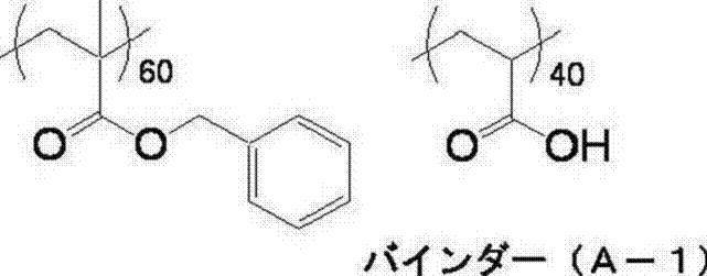
(合成例2)
<バインダー(A-2)の合成>
反応容器中に、MFG(日本乳化剤株式会社製)7.48gをあらかじめ加え、90℃に昇温し、モノマー成分としてMAA(14.65g)、MMA(0.54g)、CHMA(17.55g)、ラジカル重合開始剤としてAIBN(0.50g)、およびMFG(55.2g)からなる混合溶液を窒素ガス雰囲気下、90℃の反応容器中に2時間かけて滴下した。滴下後、4時間反応させて、アクリル樹脂溶液を得た。
次に、得られたアクリル樹脂溶液に、ハイドロキノンモノメチルエーテル0.15g、およびテトラエチルアンモニウムブロマイド0.34gを加えた後、GMA 12.26gを2時間かけて滴下した。滴下後、空気を吹き込みながら90℃で4時間反応させた後、固形分濃度が45%になるようにPGMEAを添加することにより調製し、バインダー(A-2)の溶液(固形分濃度:45%)を得た。
分子量はゲルパーミエーションクロマトグラフィ(GPC)を用いて測定した結果、ポリスチレン換算による重量平均分子量(Mw)は31,300、分子量分布(Mw/Mn)は2.32、酸価は74.5mgKOH/gであった。
<バインダー(A-2)の合成>
反応容器中に、MFG(日本乳化剤株式会社製)7.48gをあらかじめ加え、90℃に昇温し、モノマー成分としてMAA(14.65g)、MMA(0.54g)、CHMA(17.55g)、ラジカル重合開始剤としてAIBN(0.50g)、およびMFG(55.2g)からなる混合溶液を窒素ガス雰囲気下、90℃の反応容器中に2時間かけて滴下した。滴下後、4時間反応させて、アクリル樹脂溶液を得た。
次に、得られたアクリル樹脂溶液に、ハイドロキノンモノメチルエーテル0.15g、およびテトラエチルアンモニウムブロマイド0.34gを加えた後、GMA 12.26gを2時間かけて滴下した。滴下後、空気を吹き込みながら90℃で4時間反応させた後、固形分濃度が45%になるようにPGMEAを添加することにより調製し、バインダー(A-2)の溶液(固形分濃度:45%)を得た。
分子量はゲルパーミエーションクロマトグラフィ(GPC)を用いて測定した結果、ポリスチレン換算による重量平均分子量(Mw)は31,300、分子量分布(Mw/Mn)は2.32、酸価は74.5mgKOH/gであった。
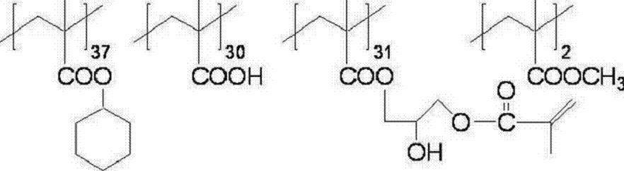
バインダー(A-2)
(調製例1)
-銀ナノワイヤー水分散液(1)の調製-
予め、下記の添加液A、G、およびHを調製した。
〔添加液A〕
硝酸銀粉末0.51gを純水50mLに溶解した。その後、1Nのアンモニア水を透明になるまで添加した。そして、全量が100mLになるように純水を添加した。
〔添加液G〕
グルコース粉末0.5gを140mLの純水で溶解して、添加液Gを調製した。
〔添加液H〕
HTAB(ヘキサデシル-トリメチルアンモニウムブロミド)粉末0.5gを27.5mLの純水で溶解して、添加液Hを調製した。
-銀ナノワイヤー水分散液(1)の調製-
予め、下記の添加液A、G、およびHを調製した。
〔添加液A〕
硝酸銀粉末0.51gを純水50mLに溶解した。その後、1Nのアンモニア水を透明になるまで添加した。そして、全量が100mLになるように純水を添加した。
〔添加液G〕
グルコース粉末0.5gを140mLの純水で溶解して、添加液Gを調製した。
〔添加液H〕
HTAB(ヘキサデシル-トリメチルアンモニウムブロミド)粉末0.5gを27.5mLの純水で溶解して、添加液Hを調製した。
次に、以下のようにして、銀ナノワイヤー水分散液を調製した。
純水410mLを三口フラスコ内に入れ、20℃にて攪拌しながら、添加液H 82.5mL、および添加液G 206mLをロートにて添加した(一段目)。この液に、添加液A 206mLを流量2.0mL/min、攪拌回転数800rpmで添加した(二段目)。その10分間後、添加液Hを82.5mL添加した(三段目)。その後、3℃/分で内温73℃まで昇温した。その後、攪拌回転数を200rpmに落とし、5.5時間加熱した。
得られた水分散液を冷却した後、限外濾過モジュールSIP1013(旭化成株式会社製、分画分子量6,000)、マグネットポンプ、およびステンレスカップをシリコーン製チューブで接続し、限外濾過装置とした。
銀ナノワイヤー分散液(水溶液)をステンレスカップに入れ、ポンプを稼動させて限外濾過を行った。モジュールからの濾液が50mLになった時点で、ステンレスカップに950mLの蒸留水を加え、洗浄を行った。前記の洗浄を伝導度が50μS/cm以下になるまで繰り返した後、濃縮を行い、0.8質量%銀ナノワイヤー水分散液を得た。
得られた調製例1の銀ナノワイヤーについて、前述のようにして平均短軸長、平均長軸長、アスペクト比が10以上の銀ナノワイヤーの比率、および銀ナノワイヤー短軸長の変動係数を測定した。
純水410mLを三口フラスコ内に入れ、20℃にて攪拌しながら、添加液H 82.5mL、および添加液G 206mLをロートにて添加した(一段目)。この液に、添加液A 206mLを流量2.0mL/min、攪拌回転数800rpmで添加した(二段目)。その10分間後、添加液Hを82.5mL添加した(三段目)。その後、3℃/分で内温73℃まで昇温した。その後、攪拌回転数を200rpmに落とし、5.5時間加熱した。
得られた水分散液を冷却した後、限外濾過モジュールSIP1013(旭化成株式会社製、分画分子量6,000)、マグネットポンプ、およびステンレスカップをシリコーン製チューブで接続し、限外濾過装置とした。
銀ナノワイヤー分散液(水溶液)をステンレスカップに入れ、ポンプを稼動させて限外濾過を行った。モジュールからの濾液が50mLになった時点で、ステンレスカップに950mLの蒸留水を加え、洗浄を行った。前記の洗浄を伝導度が50μS/cm以下になるまで繰り返した後、濃縮を行い、0.8質量%銀ナノワイヤー水分散液を得た。
得られた調製例1の銀ナノワイヤーについて、前述のようにして平均短軸長、平均長軸長、アスペクト比が10以上の銀ナノワイヤーの比率、および銀ナノワイヤー短軸長の変動係数を測定した。
その結果、平均短軸長17.2nm、平均長軸長34.2μm、変動係数が17.8%の銀ナノワイヤーを得た。得られた銀ナノワイヤーのうち、アスペクト比が10以上の銀ナノワイヤーの占める比率は81.8%であった。以後、「銀ナノワイヤー水分散液(1)」と表記する場合は、上記方法で得られた銀ナノワイヤー水分散液(1)を示す。
(調製例2)
-銀ナノワイヤーのPGMEA分散液(1)の調製-
調製例1で調製した銀ナノワイヤー水分散液(1)100部に、ポリビニルピロリドン(K-30、東京化成工業株式会社製)1部と、n-プロパノール100部を添加し、セラミックフィルターを用いたクロスフローろ過機(株)日本ガイシ製)にて10部となるまで濃縮した。次いでn-プロパノール100部およびイオン交換水100部を加え、再度クロスフローろ過機にて10部となるまで濃縮する操作を3回繰り返した。さらに前記バインダー(A-1)を1部およびn-プロパノールを10部加え、遠心分離の後、デカンテーションにて上澄みの溶媒を除去しPGMEAを添加し、再分散を行い、遠心分離から再分散までの操作を3回繰り返し、最後にPGMEAを加え、銀ナノワイヤーのPGMEA分散液を得た。最後のPGMEAの添加量は銀の含有量が、銀2%となるように調節した。分散剤として用いられたポリマーの含有量は0.05%であった。平均短軸長16.7nm、平均長軸長29.1μm、変動係数が18.2%の銀ナノワイヤーを得た。得られた銀ナノワイヤーのうち、アスペクト比が10以上の銀ナノワイヤーの占める比率は80.2%であった。以後、「銀ナノワイヤーPGMEA分散液(1)」と表記する場合は、上記方法で得られた銀ナノワイヤーPGMEA分散液(1)を示す。
(調製例3)
-ガラス基板の前処理-
まず、水酸化ナトリウム1%水溶液に浸漬した厚み0.7μmの無アルカリガラス基板を超音波洗浄機によって30分超音波照射し、ついでイオン交換水で60秒間水洗した後200℃で60分間加熱処理を行った。その後、シランカップリング液(N-β(アミノエチル)γ-アミノプロピルトリメトキシシラン0.3%水溶液、商品名:KBM603、信越化学工業(株)製)をシャワーにより20秒間吹き付け、純水シャワー洗浄した。以後、「ガラス基板」と表記する場合は、上記前処理で得られた無アルカリガラス基板を示す。
-銀ナノワイヤーのPGMEA分散液(1)の調製-
調製例1で調製した銀ナノワイヤー水分散液(1)100部に、ポリビニルピロリドン(K-30、東京化成工業株式会社製)1部と、n-プロパノール100部を添加し、セラミックフィルターを用いたクロスフローろ過機(株)日本ガイシ製)にて10部となるまで濃縮した。次いでn-プロパノール100部およびイオン交換水100部を加え、再度クロスフローろ過機にて10部となるまで濃縮する操作を3回繰り返した。さらに前記バインダー(A-1)を1部およびn-プロパノールを10部加え、遠心分離の後、デカンテーションにて上澄みの溶媒を除去しPGMEAを添加し、再分散を行い、遠心分離から再分散までの操作を3回繰り返し、最後にPGMEAを加え、銀ナノワイヤーのPGMEA分散液を得た。最後のPGMEAの添加量は銀の含有量が、銀2%となるように調節した。分散剤として用いられたポリマーの含有量は0.05%であった。平均短軸長16.7nm、平均長軸長29.1μm、変動係数が18.2%の銀ナノワイヤーを得た。得られた銀ナノワイヤーのうち、アスペクト比が10以上の銀ナノワイヤーの占める比率は80.2%であった。以後、「銀ナノワイヤーPGMEA分散液(1)」と表記する場合は、上記方法で得られた銀ナノワイヤーPGMEA分散液(1)を示す。
(調製例3)
-ガラス基板の前処理-
まず、水酸化ナトリウム1%水溶液に浸漬した厚み0.7μmの無アルカリガラス基板を超音波洗浄機によって30分超音波照射し、ついでイオン交換水で60秒間水洗した後200℃で60分間加熱処理を行った。その後、シランカップリング液(N-β(アミノエチル)γ-アミノプロピルトリメトキシシラン0.3%水溶液、商品名:KBM603、信越化学工業(株)製)をシャワーにより20秒間吹き付け、純水シャワー洗浄した。以後、「ガラス基板」と表記する場合は、上記前処理で得られた無アルカリガラス基板を示す。
(調製例4)
-PET基板の前処理-
下記の配合で接着用溶液1を調製した。
[接着用溶液1]
・タケラックWS-4000 5.0部
(固形分濃度30%、三井化学(株)製)
・界面活性剤 0.3部
(ナローアクティHN-100、三洋化成工業(株)製)
・界面活性剤 0.3部
(サンデットBL、固形分濃度43%、三洋化成工業(株)製)
・水 94.4部
-PET基板の前処理-
下記の配合で接着用溶液1を調製した。
[接着用溶液1]
・タケラックWS-4000 5.0部
(固形分濃度30%、三井化学(株)製)
・界面活性剤 0.3部
(ナローアクティHN-100、三洋化成工業(株)製)
・界面活性剤 0.3部
(サンデットBL、固形分濃度43%、三洋化成工業(株)製)
・水 94.4部
厚さ125μmのPET基板の一方の面にコロナ放電処理を施した。このコロナ放電処理を施した面に、上記の接着用溶液を塗布し120℃で2分乾燥させて、厚さが0.11μmの接着層1を形成した。
以下の配合で、接着用溶液2を調製した。
[接着用溶液2]
・テトラエトキシシラン 5.0部
(KBE-04、信越化学工業(株)製)
・3-グリシドキシプロピルトリメトキシシラン 3.2部
(KBM-403、信越化学工業(株)製)
・2-(3,4-エポキシシクロヘキシル)エチルトリメトキシシラン
(KBM-303、信越化学工業(株)製) 1.8部
・酢酸水溶液(酢酸濃度=0.05%、pH=5.2) 10.0部
・硬化剤 0.8部
(ホウ酸、和光純薬工業(株)製)
・コロイダルシリカ 60.0部
(スノーテックスO、平均粒子径10nm~20nm、固形分濃度20%、
pH=2.6、日産化学工業(株)製)
・界面活性剤 0.2部
(ナローアクティHN-100、三洋化成工業(株)製)
・界面活性剤 0.2部
(サンデットBL、固形分濃度43%、三洋化成工業(株)製)
[接着用溶液2]
・テトラエトキシシラン 5.0部
(KBE-04、信越化学工業(株)製)
・3-グリシドキシプロピルトリメトキシシラン 3.2部
(KBM-403、信越化学工業(株)製)
・2-(3,4-エポキシシクロヘキシル)エチルトリメトキシシラン
(KBM-303、信越化学工業(株)製) 1.8部
・酢酸水溶液(酢酸濃度=0.05%、pH=5.2) 10.0部
・硬化剤 0.8部
(ホウ酸、和光純薬工業(株)製)
・コロイダルシリカ 60.0部
(スノーテックスO、平均粒子径10nm~20nm、固形分濃度20%、
pH=2.6、日産化学工業(株)製)
・界面活性剤 0.2部
(ナローアクティHN-100、三洋化成工業(株)製)
・界面活性剤 0.2部
(サンデットBL、固形分濃度43%、三洋化成工業(株)製)
接着用溶液2は、以下の方法で調製した。酢酸水溶液を激しく攪拌しながら、3-グリシドキシプロピルトリメトキシシランを、この酢酸水溶液中に3分間かけて滴下した。次に、2-(3,4-エポキシシクロヘキシル)エチルトリメトキシシランを酢酸水溶液中に強く攪拌しながら3分間かけて添加した。次に、テトラメトキシシランを、酢酸水溶液中に強く攪拌しながら5分かけて添加し、その後2時間攪拌を続けた。次に、コロイダルシリカと、硬化剤と、界面活性剤とを順次添加し、接着用溶液2を調製した。
この接着用溶液2をコロナ放電処理を施した接着層1の上にバーコート法により塗布し、170℃で5分間加熱して乾燥し、厚さ4.1μmの接着層2を形成した。その後、接着層2の上にコロナ放電処理を施し、前処理PET基板を得た。以後、「PET基板」と表記する場合は、上記前処理で得られたPET基板を示す。
(実施例1)
<<導電性層の形成>>
以下の組成を有する光重合性組成物を調製した。
<光重合性組成物>
・ポリマー:(前記合成例で得られたバインダー(A-1)、
固形分45%PGMEA溶液) 44.50部
・ポリマー:(前記合成例で得られたバインダー(A-2)、
固形分45%PGMEA、MFG混合溶液) 44.50部
・重合性化合物:ジペンタエリスリトールヘキサアクリレート 8.01部
・光重合開始剤:2,4-ビス(トリクロロメチル)-6-[4-N,N-ビス(エトキシカルボニルメチル)アミノ-3-ブロモフェニル]-s-トリアジン
0.79部
・重合禁止剤:フェノチアジン 0.062部
・界面活性剤:メガファックF784F(DIC(株)製)
2.70部
・界面活性剤:ソルスパース20000(日本ルーブリゾール(株)製)
1.00部
・溶媒(PGMEA) 48.42部
・溶媒(MEK) 100.00部
得られた前記光重合性組成物3.21部、前記銀ナノワイヤーPGMEA分散液(1)6.41部、および、溶媒(PGMEA/MEK=1/1)40.38部を攪拌、混合することによって、光重合性導電性層塗布液を得た。
上記で得られた光重合性導電性層塗布液を光重合性組成物の固形分塗布量が0.175g/m2、銀量が0.035g/m2となるようにPET基板にバーコートし室温で5分間乾燥して、感光性導電性層を設けた。この感光性導電性層の厚さは0.12μmであった。
ここで、厚さは以下の方法で測定した。感光性導電性層以外の厚さについても同様である。
導電性部材上にカーボンおよびPtの保護層を形成したのち、日立社製FB-2100型収束イオンビーム装置内で約10μm幅、約100nm厚の切片を作製し作製、導電性層の断面を日立製HD-2300型STEM(印加電圧200kV)で観察し、導電性層の厚さを測定した。なお、膜厚は触針式表面形状測定器Dektak150(ULVAC社製)を用いて、導電性層を形成した部分と導電性層を除去した部分の段差から測定する簡易方法もあるが、この方法では導電性層を除去する際に基板の一部まで除去してしまう恐れがあること、さらに得られた導電性層が薄膜なため誤差が生じやすい問題があった。そこで、本明細書においては、より正確な膜厚の測定方法である上記の電子顕微鏡による導電性層断面の直接観察により求めた値を記載した。
<<導電性層の形成>>
以下の組成を有する光重合性組成物を調製した。
<光重合性組成物>
・ポリマー:(前記合成例で得られたバインダー(A-1)、
固形分45%PGMEA溶液) 44.50部
・ポリマー:(前記合成例で得られたバインダー(A-2)、
固形分45%PGMEA、MFG混合溶液) 44.50部
・重合性化合物:ジペンタエリスリトールヘキサアクリレート 8.01部
・光重合開始剤:2,4-ビス(トリクロロメチル)-6-[4-N,N-ビス(エトキシカルボニルメチル)アミノ-3-ブロモフェニル]-s-トリアジン
0.79部
・重合禁止剤:フェノチアジン 0.062部
・界面活性剤:メガファックF784F(DIC(株)製)
2.70部
・界面活性剤:ソルスパース20000(日本ルーブリゾール(株)製)
1.00部
・溶媒(PGMEA) 48.42部
・溶媒(MEK) 100.00部
得られた前記光重合性組成物3.21部、前記銀ナノワイヤーPGMEA分散液(1)6.41部、および、溶媒(PGMEA/MEK=1/1)40.38部を攪拌、混合することによって、光重合性導電性層塗布液を得た。
上記で得られた光重合性導電性層塗布液を光重合性組成物の固形分塗布量が0.175g/m2、銀量が0.035g/m2となるようにPET基板にバーコートし室温で5分間乾燥して、感光性導電性層を設けた。この感光性導電性層の厚さは0.12μmであった。
ここで、厚さは以下の方法で測定した。感光性導電性層以外の厚さについても同様である。
導電性部材上にカーボンおよびPtの保護層を形成したのち、日立社製FB-2100型収束イオンビーム装置内で約10μm幅、約100nm厚の切片を作製し作製、導電性層の断面を日立製HD-2300型STEM(印加電圧200kV)で観察し、導電性層の厚さを測定した。なお、膜厚は触針式表面形状測定器Dektak150(ULVAC社製)を用いて、導電性層を形成した部分と導電性層を除去した部分の段差から測定する簡易方法もあるが、この方法では導電性層を除去する際に基板の一部まで除去してしまう恐れがあること、さらに得られた導電性層が薄膜なため誤差が生じやすい問題があった。そこで、本明細書においては、より正確な膜厚の測定方法である上記の電子顕微鏡による導電性層断面の直接観察により求めた値を記載した。
<露光工程>
基板上の感光性導電性層に、窒素雰囲気下で超高圧水銀灯i線(365nm)を用いて、露光量40mJ/cm2でマスクを通して露光した。ここで露光はマスクを介して行い、マスクは導電性、光学特性、膜強度評価用の均一露光部およびパターニング性評価用のストライプパターン(ライン/スペース=50μm/50μm)を有していた。
基板上の感光性導電性層に、窒素雰囲気下で超高圧水銀灯i線(365nm)を用いて、露光量40mJ/cm2でマスクを通して露光した。ここで露光はマスクを介して行い、マスクは導電性、光学特性、膜強度評価用の均一露光部およびパターニング性評価用のストライプパターン(ライン/スペース=50μm/50μm)を有していた。
<現像工程>
露光後の感光性導電性層を炭酸Na系現像液(0.06モル/リットルの炭酸水素ナトリウム、同濃度の炭酸ナトリウム、1%のジブチルナフタレンスルホン酸ナトリウム、アニオン性界面活性剤、消泡剤、安定剤含有、商品名:T-CD1、富士フイルム(株)製)を用い、20℃30秒、コーン型ノズル圧力0.15MPaでシャワー現像して、未露光部の感光性導電性層を除去し、室温乾燥させた。次いで、100℃、15分間熱処理を施した。かくして、導電性領域と非導電性領域を含む導電性層を形成した。この導電性領域の厚さは0.010μmであった。
露光後の感光性導電性層を炭酸Na系現像液(0.06モル/リットルの炭酸水素ナトリウム、同濃度の炭酸ナトリウム、1%のジブチルナフタレンスルホン酸ナトリウム、アニオン性界面活性剤、消泡剤、安定剤含有、商品名:T-CD1、富士フイルム(株)製)を用い、20℃30秒、コーン型ノズル圧力0.15MPaでシャワー現像して、未露光部の感光性導電性層を除去し、室温乾燥させた。次いで、100℃、15分間熱処理を施した。かくして、導電性領域と非導電性領域を含む導電性層を形成した。この導電性領域の厚さは0.010μmであった。
<<保護層の形成>>
下記組成のゾルゲル塗布液を60℃で1時間撹拌して均一になったことを確認した。得られたゾルゲル塗布液を蒸留水で希釈しアプリケーターコートで固形分塗布量が0.50g/m2となるように上記導電性領域と非導電性領域を含む導電性層上に塗布したのち、140℃で1分間乾燥し、ゾルゲル反応を起こさせて保護層を形成し、実施例1の導電性部材を得た。上記保護層の厚みは、0.13μmであった。
<ゾルゲル塗布液>
・3-グリシドキシプロピルトリメトキシシラン 5.9部
(KBM-403、信越化学工業(株)製)
・テトラエトキシシラン 6.8部
(KBE-04、信越化学工業(株)製)
・1%酢酸水溶液 15.0部
下記組成のゾルゲル塗布液を60℃で1時間撹拌して均一になったことを確認した。得られたゾルゲル塗布液を蒸留水で希釈しアプリケーターコートで固形分塗布量が0.50g/m2となるように上記導電性領域と非導電性領域を含む導電性層上に塗布したのち、140℃で1分間乾燥し、ゾルゲル反応を起こさせて保護層を形成し、実施例1の導電性部材を得た。上記保護層の厚みは、0.13μmであった。
<ゾルゲル塗布液>
・3-グリシドキシプロピルトリメトキシシラン 5.9部
(KBM-403、信越化学工業(株)製)
・テトラエトキシシラン 6.8部
(KBE-04、信越化学工業(株)製)
・1%酢酸水溶液 15.0部
(実施例2~16)
実施例1において、ゾルゲル塗布液に含まれる3-グリシドキシプロピルトリメトキシシランとテトラエトキシシランの両者を、下記に記載した化合物(一つまたは二つ)および量に変更した以外は実施例1と同様にして実施例2~16の導電性部材を得た。得られた導電性部材の保護層の厚みも下記に示す。
実施例2:3-グリシドキシプロピルトリメトキシシラン 12.7部
(厚み:0.14μm)
実施例3:テトラエトキシシラン 12.7部
(厚み:0.12μm)
実施例4:3-グリシドキシプロピルトリメトキシシラン 0.6部
(厚み:0.13μm)
テトラエトキシシラン 12.1部
実施例5:3-グリシドキシプロピルトリメトキシシラン 1.3部
(厚み:0.13μm)
テトラエトキシシラン 11.4部
実施例6:3-グリシドキシプロピルトリメトキシシラン 3.8部
(厚み:0.13μm)
テトラエトキシシラン 8.9部
実施例7:3-グリシドキシプロピルトリメトキシシラン 6.35部
(厚み:0.13μm)
テトラエトキシシラン 6.35部
実施例8:3-グリシドキシプロピルトリメトキシシラン 10.2部
テトラエトキシシラン 2.5部
(厚み:0.13μm)
実施例9:3-グリシドキシプロピルトリメトキシシラン 12.5部
テトラエトキシシラン 0.2部
(厚み:0.13μm)
実施例10:テトラプロポキシチタネート 12.7部
(厚み:0.12μm)
実施例11:テトラエトキシジルコネート 12.7部
(厚み:0.12μm)
実施例12:2-(3,4-エポキシシクロヘキシル)エチルトリメトキシシラン
5.9部
テトラメトキシシラン 6.8部
(厚み:0.14μm)
実施例13:ウレイドプロピルトリエトキシシラン 5.9部
テトラエトキシシラン 6.8部
(厚み:0.14μm)
実施例14:ジエチルジメトキシシラン 5.9部
テトラエトキシシラン 6.8部
(厚み:0.13μm)
実施例15:プロピルトリエトキシチタネート 5.9部
テトライソプロポキシチタネート 6.8部
(厚み:0.12μm)
実施例16:エチルトリエトキシジルコネート 5.9部
テトラプロポキシジルコネート 6.8部
(厚み:0.12μm)
実施例1において、ゾルゲル塗布液に含まれる3-グリシドキシプロピルトリメトキシシランとテトラエトキシシランの両者を、下記に記載した化合物(一つまたは二つ)および量に変更した以外は実施例1と同様にして実施例2~16の導電性部材を得た。得られた導電性部材の保護層の厚みも下記に示す。
実施例2:3-グリシドキシプロピルトリメトキシシラン 12.7部
(厚み:0.14μm)
実施例3:テトラエトキシシラン 12.7部
(厚み:0.12μm)
実施例4:3-グリシドキシプロピルトリメトキシシラン 0.6部
(厚み:0.13μm)
テトラエトキシシラン 12.1部
実施例5:3-グリシドキシプロピルトリメトキシシラン 1.3部
(厚み:0.13μm)
テトラエトキシシラン 11.4部
実施例6:3-グリシドキシプロピルトリメトキシシラン 3.8部
(厚み:0.13μm)
テトラエトキシシラン 8.9部
実施例7:3-グリシドキシプロピルトリメトキシシラン 6.35部
(厚み:0.13μm)
テトラエトキシシラン 6.35部
実施例8:3-グリシドキシプロピルトリメトキシシラン 10.2部
テトラエトキシシラン 2.5部
(厚み:0.13μm)
実施例9:3-グリシドキシプロピルトリメトキシシラン 12.5部
テトラエトキシシラン 0.2部
(厚み:0.13μm)
実施例10:テトラプロポキシチタネート 12.7部
(厚み:0.12μm)
実施例11:テトラエトキシジルコネート 12.7部
(厚み:0.12μm)
実施例12:2-(3,4-エポキシシクロヘキシル)エチルトリメトキシシラン
5.9部
テトラメトキシシラン 6.8部
(厚み:0.14μm)
実施例13:ウレイドプロピルトリエトキシシラン 5.9部
テトラエトキシシラン 6.8部
(厚み:0.14μm)
実施例14:ジエチルジメトキシシラン 5.9部
テトラエトキシシラン 6.8部
(厚み:0.13μm)
実施例15:プロピルトリエトキシチタネート 5.9部
テトライソプロポキシチタネート 6.8部
(厚み:0.12μm)
実施例16:エチルトリエトキシジルコネート 5.9部
テトラプロポキシジルコネート 6.8部
(厚み:0.12μm)
(実施例17~21)
実施例1において、保護層を形成するためのゾルゲル塗布液の固形分塗布量を下記のように変更した以外は実施例1と同様にして、実施例17~21の導電性部材を得た。各保護層の厚みは、下記のとおりであった。
実施例17:1.00g/m2(厚み:0.250μm)
実施例18:0.35g/m2(厚み:0.092μm)
実施例19:0.15g/m2(厚み:0.040μm)
実施例20:0.10g/m2(厚み:0.026μm)
実施例21:0.05g/m2(厚み:0.013μm)
実施例1において、保護層を形成するためのゾルゲル塗布液の固形分塗布量を下記のように変更した以外は実施例1と同様にして、実施例17~21の導電性部材を得た。各保護層の厚みは、下記のとおりであった。
実施例17:1.00g/m2(厚み:0.250μm)
実施例18:0.35g/m2(厚み:0.092μm)
実施例19:0.15g/m2(厚み:0.040μm)
実施例20:0.10g/m2(厚み:0.026μm)
実施例21:0.05g/m2(厚み:0.013μm)
(実施例22~26)
実施例3において、ゾルゲル塗布液の固形分塗布量を下記のように変更した以外は実施例3と同様にして、実施例22~26の導電性部材を得た。各導電性層の厚みは、下記のとおりであった。
実施例22:1.00g/m2(厚み:0.245μm)
実施例23:0.35g/m2(厚み:0.090μm)
実施例24:0.15g/m2(厚み:0.039μm)
実施例25:0.10g/m2(厚み:0.025μm)
実施例26:0.05g/m2(厚み:0.013μm)
実施例3において、ゾルゲル塗布液の固形分塗布量を下記のように変更した以外は実施例3と同様にして、実施例22~26の導電性部材を得た。各導電性層の厚みは、下記のとおりであった。
実施例22:1.00g/m2(厚み:0.245μm)
実施例23:0.35g/m2(厚み:0.090μm)
実施例24:0.15g/m2(厚み:0.039μm)
実施例25:0.10g/m2(厚み:0.025μm)
実施例26:0.05g/m2(厚み:0.013μm)
(実施例27~30)
実施例1で用いた光重合性導電性層塗布液を用いて、光重合性組成物の固形分塗布量および銀量を下記のように変更した以外は実施例1と同様にして、実施例27~30の導電性部材を得た。露光工程および現像工程を行った後の各導電性層の厚みは、下記のとおりであった。保護層の厚みはすべて0.13μmであった。
実施例27:固形分塗布量0.500g/m2、銀量0.100g/m2(厚み:0.029μm)
実施例28:固形分塗布量0.100g/m2、銀量0.020g/m2(厚み:0.006μm)
実施例29:固形分塗布量0.050g/m2、銀量0.010g/m2(厚み:0.003μm)
実施例30:固形分塗布量0.025g/m2、銀量0.005g/m2(厚み:0.001μm)
実施例1で用いた光重合性導電性層塗布液を用いて、光重合性組成物の固形分塗布量および銀量を下記のように変更した以外は実施例1と同様にして、実施例27~30の導電性部材を得た。露光工程および現像工程を行った後の各導電性層の厚みは、下記のとおりであった。保護層の厚みはすべて0.13μmであった。
実施例27:固形分塗布量0.500g/m2、銀量0.100g/m2(厚み:0.029μm)
実施例28:固形分塗布量0.100g/m2、銀量0.020g/m2(厚み:0.006μm)
実施例29:固形分塗布量0.050g/m2、銀量0.010g/m2(厚み:0.003μm)
実施例30:固形分塗布量0.025g/m2、銀量0.005g/m2(厚み:0.001μm)
(実施例31~36)
実施例1で用いた光重合性組成物、銀ナノワイヤーPGMEA分散液(1)、および、溶媒(PGMEA/MEK=1/1)の混合比を適宜変更し、光重合性組成物の固形分塗布量および銀量が下記のとおりとなるように変更した以外は実施例1と同様にして、実施例31~36の導電性部材を得た。露光工程および現像工程を行った後の各導電性層の厚みは、下記のとおりであった。保護層の厚みはすべて0.13μmであった。
実施例31:固形分塗布量0.280g/m2、銀量0.035g/m2(厚み:0.016μm)
実施例32:固形分塗布量0.210g/m2、銀量0.035g/m2(厚み:0.012μm)
実施例33:固形分塗布量0.160g/m2、銀量0.020g/m2(厚み:0.009μm)
実施例34:固形分塗布量0.120g/m2、銀量0.020g/m2(厚み:0.007μm)
実施例35:固形分塗布量0.120g/m2、銀量0.015g/m2(厚み:0.007μm)
実施例36:固形分塗布量0.090g/m2、銀量0.015g/m2(厚み:0.005μm)
(実施例37)
実施例1においてPET基板をガラス基板に変更した以外は実施例1と同様にして、実施例37の導電性部材を得た。露光工程および現像工程を行った後の導電性層の厚み0.010μmで、保護層の厚みは0.13μmであった。
実施例1で用いた光重合性組成物、銀ナノワイヤーPGMEA分散液(1)、および、溶媒(PGMEA/MEK=1/1)の混合比を適宜変更し、光重合性組成物の固形分塗布量および銀量が下記のとおりとなるように変更した以外は実施例1と同様にして、実施例31~36の導電性部材を得た。露光工程および現像工程を行った後の各導電性層の厚みは、下記のとおりであった。保護層の厚みはすべて0.13μmであった。
実施例31:固形分塗布量0.280g/m2、銀量0.035g/m2(厚み:0.016μm)
実施例32:固形分塗布量0.210g/m2、銀量0.035g/m2(厚み:0.012μm)
実施例33:固形分塗布量0.160g/m2、銀量0.020g/m2(厚み:0.009μm)
実施例34:固形分塗布量0.120g/m2、銀量0.020g/m2(厚み:0.007μm)
実施例35:固形分塗布量0.120g/m2、銀量0.015g/m2(厚み:0.007μm)
実施例36:固形分塗布量0.090g/m2、銀量0.015g/m2(厚み:0.005μm)
(実施例37)
実施例1においてPET基板をガラス基板に変更した以外は実施例1と同様にして、実施例37の導電性部材を得た。露光工程および現像工程を行った後の導電性層の厚み0.010μmで、保護層の厚みは0.13μmであった。
(実施例38~45)
実施例1にて使用した銀ナノワイヤーPGMEA分散液(1)を、銀ナノワイヤーの平均長軸長および平均短軸長が下記表1に示される銀ナノワイヤーPGMEA分散液(2)~(9)に変更した以外は実施例1と同様にして、実施例38~45の導電性部材を得た。
実施例1にて使用した銀ナノワイヤーPGMEA分散液(1)を、銀ナノワイヤーの平均長軸長および平均短軸長が下記表1に示される銀ナノワイヤーPGMEA分散液(2)~(9)に変更した以外は実施例1と同様にして、実施例38~45の導電性部材を得た。
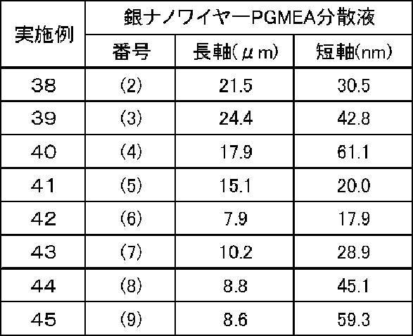
(比較例1)
実施例1において、保護層を下記の保護層C1に変更した以外は実施例1と同様にして、比較例1の導電性部材を得た。
下記組成の塗布液Aを固形分量0.50g/m2になるように塗布し、窒素雰囲気下で超高圧水銀灯i線(365nm)を用いて、露光量40mJ/cm2で露光し保護層C1を形成した。
<塗布液A>
・ジペンタエリスリトールヘキサアクリレート 8.01部
・光重合開始剤:2,4-ビス(トリクロロメチル)-6-[4-N,N-ビス(エトキシカルボニルメチル)アミノ-3-ブロモフェニル]-s-トリアジン
0.79部
・界面活性剤:メガファックF784F(DIC(株)製)
2.70部
・溶媒(PGMEA) 356.54部
実施例1において、保護層を下記の保護層C1に変更した以外は実施例1と同様にして、比較例1の導電性部材を得た。
下記組成の塗布液Aを固形分量0.50g/m2になるように塗布し、窒素雰囲気下で超高圧水銀灯i線(365nm)を用いて、露光量40mJ/cm2で露光し保護層C1を形成した。
<塗布液A>
・ジペンタエリスリトールヘキサアクリレート 8.01部
・光重合開始剤:2,4-ビス(トリクロロメチル)-6-[4-N,N-ビス(エトキシカルボニルメチル)アミノ-3-ブロモフェニル]-s-トリアジン
0.79部
・界面活性剤:メガファックF784F(DIC(株)製)
2.70部
・溶媒(PGMEA) 356.54部
<<評価>>
得られた各導電性部材について、以下に記載する方法で表面抵抗率、光学特性(全光透過率、ヘイズ)、膜強度、耐摩耗性、耐熱性、耐湿熱性および屈曲性を評価した。
得られた各導電性部材について、以下に記載する方法で表面抵抗率、光学特性(全光透過率、ヘイズ)、膜強度、耐摩耗性、耐熱性、耐湿熱性および屈曲性を評価した。
<表面抵抗率>
導電性部材の導電性領域の表面抵抗率を、三菱化学株式会社製Loresta-GP MCP-T600を用いて測定し、その値から下記のランク付けを行った。
・ランク5:表面抵抗率が100Ω/□未満で、極めて優秀なレベル
・ランク4:表面抵抗率が100Ω/□以上、150Ω/□未満で、優秀なレベル
・ランク3:表面抵抗率が150Ω/□以上、200Ω/□未満で、許容レベル
・ランク2:表面抵抗率が200Ω/□以上、1000Ω/□未満で、やや問題なレベル・ランク1:表面抵抗率が1000Ω/□以上で、問題なレベル。
導電性部材の導電性領域の表面抵抗率を、三菱化学株式会社製Loresta-GP MCP-T600を用いて測定し、その値から下記のランク付けを行った。
・ランク5:表面抵抗率が100Ω/□未満で、極めて優秀なレベル
・ランク4:表面抵抗率が100Ω/□以上、150Ω/□未満で、優秀なレベル
・ランク3:表面抵抗率が150Ω/□以上、200Ω/□未満で、許容レベル
・ランク2:表面抵抗率が200Ω/□以上、1000Ω/□未満で、やや問題なレベル・ランク1:表面抵抗率が1000Ω/□以上で、問題なレベル。
<光学特性(全光透過率)>
導電性部材の導電性領域に相当する部分の全光透過率(%)と、導電性層20を形成する前のPET基板101(実施例1~36)またはガラス基板(実施例37)の全光透過率(%)をガードナー社製のヘイズガードプラスを用いて測定し、その比から透明導電膜の透過率を換算し、下記のランク付けを行った。測定はC光源下のCIE視感度関数yについて、測定角0°で測定し、下記のランク付けを行った。
・ランクA:透過率90%以上で、良好なレベル
・ランクB:透過率85%以上90%未満で、やや問題なレベル
導電性部材の導電性領域に相当する部分の全光透過率(%)と、導電性層20を形成する前のPET基板101(実施例1~36)またはガラス基板(実施例37)の全光透過率(%)をガードナー社製のヘイズガードプラスを用いて測定し、その比から透明導電膜の透過率を換算し、下記のランク付けを行った。測定はC光源下のCIE視感度関数yについて、測定角0°で測定し、下記のランク付けを行った。
・ランクA:透過率90%以上で、良好なレベル
・ランクB:透過率85%以上90%未満で、やや問題なレベル
<光学特性(ヘイズ)>
導電性部材の導電性領域に相当する部分のヘイズをガードナー社製のヘイズガードプラスを用いて測定し、下記のランク付けを行った。
・ランクA:ヘイズが1.5%未満で、優秀なレベル
・ランクB:ヘイズが1.5%以上2.0%未満で、良好なレベル。
・ランクC:ヘイズが2.0%以上2.5%未満で、やや問題なレベル。
・ランクD:ヘイズが2.5%以上で、問題なレベル。
導電性部材の導電性領域に相当する部分のヘイズをガードナー社製のヘイズガードプラスを用いて測定し、下記のランク付けを行った。
・ランクA:ヘイズが1.5%未満で、優秀なレベル
・ランクB:ヘイズが1.5%以上2.0%未満で、良好なレベル。
・ランクC:ヘイズが2.0%以上2.5%未満で、やや問題なレベル。
・ランクD:ヘイズが2.5%以上で、問題なレベル。
<膜強度>
日本塗料検査協会検定鉛筆引っかき用鉛筆(硬度HBおよび硬度B)をJIS K5600-5-4に準じてセットした鉛筆引掻塗膜硬さ試験機(株式会社東洋精機製作所製、型式NP)にて荷重500gの条件で長さ10mmにわたり引っ掻いた後、下記条件にて露光および現像を施し、引っ掻いた部分をデジタルマイクロスコープ(VHX-600、キーエンス株式会社製、倍率2,000倍)で観察し、下記のランク付けを行った。なお、ランク3以上では導電性層中の金属ナノワイヤーの断線が見られず、実用上の導電性の確保が可能な問題の無いレベルである。
〔評価基準〕
・ランク5:硬度2Hの鉛筆引っ掻きで引っ掻き跡が認められず、極めて優秀なレベル。・ランク4:硬度2Hの鉛筆引っ掻きで金属ナノワイヤーが削られ、引っ掻き跡が認められるものの、金属ナノワイヤーが残存し、基材表面の露出が観察されない、優秀なレベル。
・ランク3:硬度2Hの鉛筆引っ掻きで基材表面の露出が観察されるものの、硬度HBの鉛筆引っ掻きで金属ナノワイヤーが残存し、基材表面の露出が観察されない、良好なレベル。
・ランク2:硬度HBの鉛筆で導電性層が削られ、基材表面の露出が部分的に観察される、問題なレベル。
・ランク1:硬度HBの鉛筆で導電性層が削られ、基材表面の殆どが露出している、極めて問題なレベル。
日本塗料検査協会検定鉛筆引っかき用鉛筆(硬度HBおよび硬度B)をJIS K5600-5-4に準じてセットした鉛筆引掻塗膜硬さ試験機(株式会社東洋精機製作所製、型式NP)にて荷重500gの条件で長さ10mmにわたり引っ掻いた後、下記条件にて露光および現像を施し、引っ掻いた部分をデジタルマイクロスコープ(VHX-600、キーエンス株式会社製、倍率2,000倍)で観察し、下記のランク付けを行った。なお、ランク3以上では導電性層中の金属ナノワイヤーの断線が見られず、実用上の導電性の確保が可能な問題の無いレベルである。
〔評価基準〕
・ランク5:硬度2Hの鉛筆引っ掻きで引っ掻き跡が認められず、極めて優秀なレベル。・ランク4:硬度2Hの鉛筆引っ掻きで金属ナノワイヤーが削られ、引っ掻き跡が認められるものの、金属ナノワイヤーが残存し、基材表面の露出が観察されない、優秀なレベル。
・ランク3:硬度2Hの鉛筆引っ掻きで基材表面の露出が観察されるものの、硬度HBの鉛筆引っ掻きで金属ナノワイヤーが残存し、基材表面の露出が観察されない、良好なレベル。
・ランク2:硬度HBの鉛筆で導電性層が削られ、基材表面の露出が部分的に観察される、問題なレベル。
・ランク1:硬度HBの鉛筆で導電性層が削られ、基材表面の殆どが露出している、極めて問題なレベル。
<耐摩耗性>
導電性部材の保護層の表面をガーゼを用いて20mm×20mmのサイズで500g荷重で50往復擦る磨耗処理を行い、その前後の傷の有無を観察すると共に、表面抵抗率の変化率(摩耗処理後の表面抵抗率/摩耗処理前の表面抵抗率)を算出した。摩耗試験には、新東科学株式会社製の連続加重引掻試験機Type18s、表面抵抗率は三菱化学株式会社製Loresta-GP MCP-T600を用いて測定した。傷が無く、表面抵抗率の変化率が少ないものほど(1に近いほど)、耐摩耗性に優れる。
導電性部材の保護層の表面をガーゼを用いて20mm×20mmのサイズで500g荷重で50往復擦る磨耗処理を行い、その前後の傷の有無を観察すると共に、表面抵抗率の変化率(摩耗処理後の表面抵抗率/摩耗処理前の表面抵抗率)を算出した。摩耗試験には、新東科学株式会社製の連続加重引掻試験機Type18s、表面抵抗率は三菱化学株式会社製Loresta-GP MCP-T600を用いて測定した。傷が無く、表面抵抗率の変化率が少ないものほど(1に近いほど)、耐摩耗性に優れる。
<耐熱性>
導電性部材を150℃で60分間加熱する加熱処理を行い、その前後の表面抵抗率の変化率(加熱処理後表面抵抗率/加熱処理前表面抵抗率)およびヘイズの変化量(加熱処理後表ヘイズ-加熱処理前ヘイズ)を算出した。表面抵抗値は三菱化学株式会社製Loresta-GP MCP-T600を用い、ヘイズはガードナー社製のヘイズガードプラスを用いて測定した。表面抵抗率の変化率が1に近いほど、そしてヘイズの変化量が少ないものほど、耐熱性に優れる。
導電性部材を150℃で60分間加熱する加熱処理を行い、その前後の表面抵抗率の変化率(加熱処理後表面抵抗率/加熱処理前表面抵抗率)およびヘイズの変化量(加熱処理後表ヘイズ-加熱処理前ヘイズ)を算出した。表面抵抗値は三菱化学株式会社製Loresta-GP MCP-T600を用い、ヘイズはガードナー社製のヘイズガードプラスを用いて測定した。表面抵抗率の変化率が1に近いほど、そしてヘイズの変化量が少ないものほど、耐熱性に優れる。
<耐湿熱性>
導電性部材を60℃90RH%の環境下で240時間静置する湿熱処理を行い、その前後の表面抵抗率の変化率(湿熱処理後表面抵抗率/湿熱処理前表面抵抗率)およびヘイズの変化量(湿熱処理後ヘイズ-湿熱処理前ヘイズ)を算出した。表面抵抗率は三菱化学株式会社製Loresta-GP MCP-T600を用い、ヘイズはガードナー社製のヘイズガードプラスを用いて測定した。表面抵抗率の変化率が1に近いほど、そしてヘイズの変化量が少ないものほど、耐湿熱性に優れる。
導電性部材を60℃90RH%の環境下で240時間静置する湿熱処理を行い、その前後の表面抵抗率の変化率(湿熱処理後表面抵抗率/湿熱処理前表面抵抗率)およびヘイズの変化量(湿熱処理後ヘイズ-湿熱処理前ヘイズ)を算出した。表面抵抗率は三菱化学株式会社製Loresta-GP MCP-T600を用い、ヘイズはガードナー社製のヘイズガードプラスを用いて測定した。表面抵抗率の変化率が1に近いほど、そしてヘイズの変化量が少ないものほど、耐湿熱性に優れる。
<屈曲性>
導電性部材をコーテック(株)社製の円筒形マンドレル屈曲試験器を用いて、直径10mmの円筒マンドレルに20回曲げる屈曲処理を行い、その前後のクラックの有無を観察すると共に、表面抵抗率の変化率(屈曲処理後の表面抵抗率/屈曲処理前の表面抵抗率)を算出した。クラックの有無は目視および光学顕微鏡を用い、表面抵抗率は三菱化学株式会社製Loresta-GP MCP-T600を用いて測定した。クラックが無く且つ表面抵抗率の変化率が1に近いほど、屈曲性に優れる。
評価結果を表2および表3に示す。
なお、表2および表3には、参考データとして、各導電性部材にける保護層形成前の表面抵抗率についての評価ランクも記載した。
導電性部材をコーテック(株)社製の円筒形マンドレル屈曲試験器を用いて、直径10mmの円筒マンドレルに20回曲げる屈曲処理を行い、その前後のクラックの有無を観察すると共に、表面抵抗率の変化率(屈曲処理後の表面抵抗率/屈曲処理前の表面抵抗率)を算出した。クラックの有無は目視および光学顕微鏡を用い、表面抵抗率は三菱化学株式会社製Loresta-GP MCP-T600を用いて測定した。クラックが無く且つ表面抵抗率の変化率が1に近いほど、屈曲性に優れる。
評価結果を表2および表3に示す。
なお、表2および表3には、参考データとして、各導電性部材にける保護層形成前の表面抵抗率についての評価ランクも記載した。
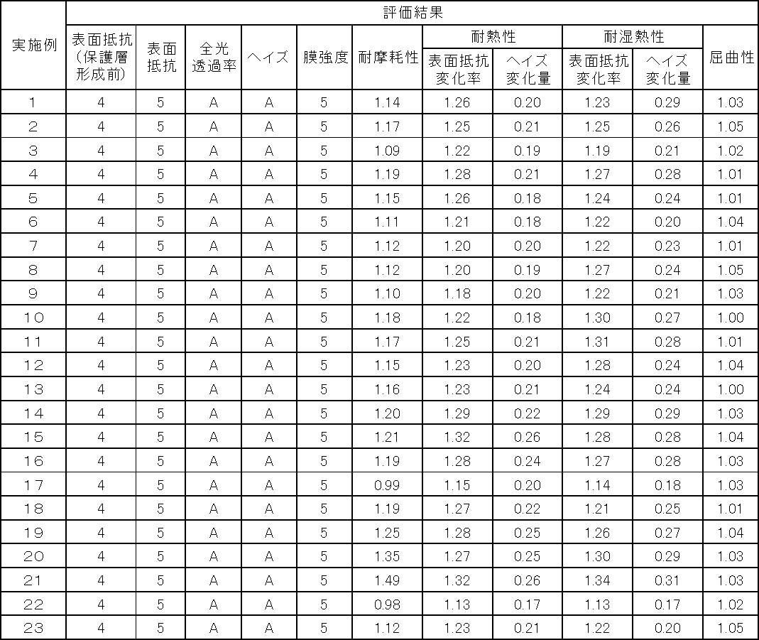

表2および表3に示された結果から、本発明に係る導電性部材は導電性と透明性が優れていると共に、耐摩耗性、耐熱性および耐湿熱性に優れると同時に、耐屈曲性に優れていることが理解できる。特に、保護層を設けたことにより、単に膜強度が著しく高まっているだけでなく、表面抵抗率が保護層を設ける前と同等か、又はそれより低い値に改善されるという著しい効果を奏していることが分かる。
(実施例46)
<<導電性層形成用積層体の調製>>
<クッション層の形成>
転写用基材(厚さ75μmのポリエチレンテレフタレートフィルム)上に、下記処方1からなる熱可塑性樹脂層用塗布液を塗布し、100℃で2分間乾燥させた後さらに120℃で1分間乾燥させ、乾燥層厚16.5μmの熱可塑性樹脂層から成るクッション層を形成した。ここで、乾燥条件における温度「100℃」および「120℃」は、いずれも基板温度である。以下の乾燥条件における温度も同様である。
<<導電性層形成用積層体の調製>>
<クッション層の形成>
転写用基材(厚さ75μmのポリエチレンテレフタレートフィルム)上に、下記処方1からなる熱可塑性樹脂層用塗布液を塗布し、100℃で2分間乾燥させた後さらに120℃で1分間乾燥させ、乾燥層厚16.5μmの熱可塑性樹脂層から成るクッション層を形成した。ここで、乾燥条件における温度「100℃」および「120℃」は、いずれも基板温度である。以下の乾燥条件における温度も同様である。
<熱可塑性樹脂層用塗布液の処方1>
・メチルメタクリレート/2-エチルヘキシルアクリレート/ベンジルメタクリレート/メタクリル酸共重合体 58.4部
(=55/11.7/4.5/28.8[モル比]、質量平均分子量90,000)
・スチレン/アクリル酸共重合体 136部
(=63/37[モル比]、質量平均分子量8,000)
・2,2-ビス〔4-(メタクリロキシポリエトキシ)フェニル〕プロパン
90.7部
・界面活性剤 メガファックF-780-F
(大日本インキ化学工業株式会社製) 5.4部
・メタノール 111部
・1-メトキシ-2-プロパノール 63.4部
・メチルエチルケトン 534部
・メチルメタクリレート/2-エチルヘキシルアクリレート/ベンジルメタクリレート/メタクリル酸共重合体 58.4部
(=55/11.7/4.5/28.8[モル比]、質量平均分子量90,000)
・スチレン/アクリル酸共重合体 136部
(=63/37[モル比]、質量平均分子量8,000)
・2,2-ビス〔4-(メタクリロキシポリエトキシ)フェニル〕プロパン
90.7部
・界面活性剤 メガファックF-780-F
(大日本インキ化学工業株式会社製) 5.4部
・メタノール 111部
・1-メトキシ-2-プロパノール 63.4部
・メチルエチルケトン 534部
次に、形成したクッション層上に、下記処方2からなる中間層用塗布液を塗布し、80℃で1分間乾燥させた後さらに120℃1分乾燥させて、乾燥層厚1.6μmの中間層を形成した。
<中間層用塗布液の処方2>
・ポリビニルアルコール 3.22部
(PVA-205、鹸化率88%、(株)クラレ製)
・ポリビニルピロリドン 1.49部
(PVP K-30、アイエスピー・ジャパン株式会社製)
・メタノール 42.9部
・蒸留水 52.4部
・ポリビニルアルコール 3.22部
(PVA-205、鹸化率88%、(株)クラレ製)
・ポリビニルピロリドン 1.49部
(PVP K-30、アイエスピー・ジャパン株式会社製)
・メタノール 42.9部
・蒸留水 52.4部
実施例1で使用した光重合性導電性層塗布液と同じものを、上記中間層上に塗布、乾燥することによって、感光性導電性層を形成し、導電性層形成用積層体を作製した。ここで非パターン化導電性層における銀量は0.035g/m2、光重合性組成物の固形分塗布量は0.175g/m2であった。
得られた上記に積層体において、感光性のマトリックスを含む感光性導電性層とクッション層との合計層厚の平均値Sと、転写用基材の厚みの平均値Nの比S/Nの値は0.223であった。
得られた上記に積層体において、感光性のマトリックスを含む感光性導電性層とクッション層との合計層厚の平均値Sと、転写用基材の厚みの平均値Nの比S/Nの値は0.223であった。
<<導電性部材の作製>>
上記導電性層形成用積層体を用いて、下記の転写工程、露光工程、現像工程、ポストベイク工程を経ることによって基材上にパターン化導電性層を有する導電性部材を作製した。
上記導電性層形成用積層体を用いて、下記の転写工程、露光工程、現像工程、ポストベイク工程を経ることによって基材上にパターン化導電性層を有する導電性部材を作製した。
(転写工程)
調整例4で得られたPET基板の表面と、上記導電性層形成用積層体の感光性導電性層の表面とが接するように重ね合わせてラミネートし、転写用基材/クッション層/中間層/感光性導電性層/PET基板の積層構造を有する積層体を形成した。
次に、上記積層体から転写用基材を剥離した。
調整例4で得られたPET基板の表面と、上記導電性層形成用積層体の感光性導電性層の表面とが接するように重ね合わせてラミネートし、転写用基材/クッション層/中間層/感光性導電性層/PET基板の積層構造を有する積層体を形成した。
次に、上記積層体から転写用基材を剥離した。
(露光工程)
PET基板上の感光性導電性層に対し、クッション層および中間層を介して超高圧水銀灯i線(365nm)を用いて、露光量40mJ/cm2でマスクを通して露光した。ここで、マスクは導電性、光学特性、膜強度評価用の均一露光部およびパターニング性評価用のストライプパターン(ライン/スペース=50μm/50μm)を有していた。
PET基板上の感光性導電性層に対し、クッション層および中間層を介して超高圧水銀灯i線(365nm)を用いて、露光量40mJ/cm2でマスクを通して露光した。ここで、マスクは導電性、光学特性、膜強度評価用の均一露光部およびパターニング性評価用のストライプパターン(ライン/スペース=50μm/50μm)を有していた。
(現像工程)
露光後の試料に、1%トリエタノールアミン水溶液を付与して熱可塑性樹脂層(クッション層)および中間層を溶解除去した。これらの層を完全に除去できる最短除去時間は30秒間であった。
次に、炭酸Na系現像液(0.06モル/リットルの炭酸水素ナトリウム、同濃度の炭酸ナトリウム、1%のジブチルナフタレンスルホン酸ナトリウム、アニオン性界面活性剤、消泡剤、安定剤含有、商品名:T-CD1、富士フイルム(株)製)を用い、前記の感光性導電性層を20℃で30秒間、コーン型ノズル圧力0.15MPaでシャワーリング現像し、室温乾燥させた。次いで、100℃、15分間熱処理を施した。かくして、導電性領域と非導電性領域を含む導電性層を形成した。この導電性領域の厚さは0.011μmであった。
露光後の試料に、1%トリエタノールアミン水溶液を付与して熱可塑性樹脂層(クッション層)および中間層を溶解除去した。これらの層を完全に除去できる最短除去時間は30秒間であった。
次に、炭酸Na系現像液(0.06モル/リットルの炭酸水素ナトリウム、同濃度の炭酸ナトリウム、1%のジブチルナフタレンスルホン酸ナトリウム、アニオン性界面活性剤、消泡剤、安定剤含有、商品名:T-CD1、富士フイルム(株)製)を用い、前記の感光性導電性層を20℃で30秒間、コーン型ノズル圧力0.15MPaでシャワーリング現像し、室温乾燥させた。次いで、100℃、15分間熱処理を施した。かくして、導電性領域と非導電性領域を含む導電性層を形成した。この導電性領域の厚さは0.011μmであった。
<<保護層の形成>>
実施例1で得られたゾルゲル塗布液と同じものを固形分塗布量が0.50g/m2となるように、パターン化導電性層上に塗布したのち、140℃で1分間乾燥し、ゾルゲル反応を起こさせ、保護層を形成し実施例46の導電性部材を得た。保護層の厚みは、0.13μmであった。
実施例1で得られたゾルゲル塗布液と同じものを固形分塗布量が0.50g/m2となるように、パターン化導電性層上に塗布したのち、140℃で1分間乾燥し、ゾルゲル反応を起こさせ、保護層を形成し実施例46の導電性部材を得た。保護層の厚みは、0.13μmであった。
(実施例47~61)
実施例46において、保護層の形成に使用したゾルゲル塗布液に含まれる3-グリシドキシプロピルトリメトキシシランとテトラエトキシシランの両者を、下記に記載した化合物(一つまたは二つ)および量に変更した以外は実施例46と同様にして、実施例47~61の導電性部材を得た。得られた導電性部材の保護層の厚みも下記に示す。
実施例47:3-グリシドキシプロピルトリメトキシシラン 12.7部
(厚み:0.14μm)
実施例48:テトラエトキシシラン 12.7部
(厚み:0.12μm)
実施例49:3-グリシドキシプロピルトリメトキシシラン 0.6部
テトラエトキシシラン 12.1部
(厚み:0.13μm)
実施例50:3-グリシドキシプロピルトリメトキシシラン 1.3部
テトラエトキシシラン 11.4部
(厚み:0.13μm)
実施例51:3-グリシドキシプロピルトリメトキシシラン 3.8部
テトラエトキシシラン 8.9部
(厚み:0.13μm)
実施例52:3-グリシドキシプロピルトリメトキシシラン 6.35部
テトラエトキシシラン 6.35部
(厚み:0.13μm)
実施例53:3-グリシドキシプロピルトリメトキシシラン 10.2部
テトラエトキシシラン 2.5部
(厚み:0.13μm)
実施例54:3-グリシドキシプロピルトリメトキシシラン 12.5部
テトラエトキシシラン 0.2部
(厚み:0.13μm)
実施例55:テトラプロポキシチタネート 12.7部
(厚み:0.12μm)
実施例56:テトラエトキシジルコネート 12.7部
(厚み:0.12μm)
実施例57:2-(3,4-エポキシシクロヘキシル)エチルトリメトキシシラン
5.9部
テトラメトキシシラン 6.8部
(厚み:0.14μm)
実施例58:ウレイドプロピルトリエトキシシラン 5.9部
テトラエトキシシラン 6.8部
(厚み:0.14μm)
実施例59:ジエチルジメトキシシラン 5.9部
テトラエトキシシラン 6.8部
(厚み:0.13μm)
実施例60:プロピルトリエトキシチタネート 5.9部
テトライソプロポキシチタネート 6.8部
(厚み:0.12μm)
実施例61:エチルトリエトキシジルコネート 5.9部
テトラプロポキシジルコネート 6.8部
(厚み:0.12μm)
実施例46において、保護層の形成に使用したゾルゲル塗布液に含まれる3-グリシドキシプロピルトリメトキシシランとテトラエトキシシランの両者を、下記に記載した化合物(一つまたは二つ)および量に変更した以外は実施例46と同様にして、実施例47~61の導電性部材を得た。得られた導電性部材の保護層の厚みも下記に示す。
実施例47:3-グリシドキシプロピルトリメトキシシラン 12.7部
(厚み:0.14μm)
実施例48:テトラエトキシシラン 12.7部
(厚み:0.12μm)
実施例49:3-グリシドキシプロピルトリメトキシシラン 0.6部
テトラエトキシシラン 12.1部
(厚み:0.13μm)
実施例50:3-グリシドキシプロピルトリメトキシシラン 1.3部
テトラエトキシシラン 11.4部
(厚み:0.13μm)
実施例51:3-グリシドキシプロピルトリメトキシシラン 3.8部
テトラエトキシシラン 8.9部
(厚み:0.13μm)
実施例52:3-グリシドキシプロピルトリメトキシシラン 6.35部
テトラエトキシシラン 6.35部
(厚み:0.13μm)
実施例53:3-グリシドキシプロピルトリメトキシシラン 10.2部
テトラエトキシシラン 2.5部
(厚み:0.13μm)
実施例54:3-グリシドキシプロピルトリメトキシシラン 12.5部
テトラエトキシシラン 0.2部
(厚み:0.13μm)
実施例55:テトラプロポキシチタネート 12.7部
(厚み:0.12μm)
実施例56:テトラエトキシジルコネート 12.7部
(厚み:0.12μm)
実施例57:2-(3,4-エポキシシクロヘキシル)エチルトリメトキシシラン
5.9部
テトラメトキシシラン 6.8部
(厚み:0.14μm)
実施例58:ウレイドプロピルトリエトキシシラン 5.9部
テトラエトキシシラン 6.8部
(厚み:0.14μm)
実施例59:ジエチルジメトキシシラン 5.9部
テトラエトキシシラン 6.8部
(厚み:0.13μm)
実施例60:プロピルトリエトキシチタネート 5.9部
テトライソプロポキシチタネート 6.8部
(厚み:0.12μm)
実施例61:エチルトリエトキシジルコネート 5.9部
テトラプロポキシジルコネート 6.8部
(厚み:0.12μm)
(実施例62~66)
実施例46において、保護層を形成するためのゾルゲル塗布液の固形分塗布量を下記のように変更した以外は実施例46と同様にして、実施例62~66の導電性部材を得た。各保護層の厚みは、下記のとおりであった。
実施例62:1.00g/m2(厚み:0.250μm)
実施例63:0.35g/m2(厚み:0.092μm)
実施例64:0.15g/m2(厚み:0.040μm)
実施例65:0.10g/m2(厚み:0.026μm)
実施例66:0.05g/m2(厚み:0.013μm)
実施例46において、保護層を形成するためのゾルゲル塗布液の固形分塗布量を下記のように変更した以外は実施例46と同様にして、実施例62~66の導電性部材を得た。各保護層の厚みは、下記のとおりであった。
実施例62:1.00g/m2(厚み:0.250μm)
実施例63:0.35g/m2(厚み:0.092μm)
実施例64:0.15g/m2(厚み:0.040μm)
実施例65:0.10g/m2(厚み:0.026μm)
実施例66:0.05g/m2(厚み:0.013μm)
(実施例67~71)
実施例48において、保護層を形成するためのゾルゲル塗布液の固形分塗布量を下記のように変更した以外は実施例48と同様にして、実施例67~71の導電性部材を得た。各保護層の厚みは、下記のとおりであった。
実施例67:1.00g/m2(厚み:0.245μm)
実施例68:0.35g/m2(厚み:0.090μm)
実施例69:0.15g/m2(厚み:0.039μm)
実施例70:0.10g/m2(厚み:0.025μm)
実施例71:0.05g/m2(厚み:0.013μm)
実施例48において、保護層を形成するためのゾルゲル塗布液の固形分塗布量を下記のように変更した以外は実施例48と同様にして、実施例67~71の導電性部材を得た。各保護層の厚みは、下記のとおりであった。
実施例67:1.00g/m2(厚み:0.245μm)
実施例68:0.35g/m2(厚み:0.090μm)
実施例69:0.15g/m2(厚み:0.039μm)
実施例70:0.10g/m2(厚み:0.025μm)
実施例71:0.05g/m2(厚み:0.013μm)
(実施例72~75)
実施例46で用いた光重合性導電性層塗布液と同じものを用いて、光重合性組成物の固形分塗布量および銀量を下記のとおりとなるように変更した以外は実施例46と同様にして、実施例72~75の導電性部材を得た。各導電性層の厚みは、下記のとおりであった。
実施例72:光重合性組成物固形分塗布量0.500g/m2、銀量0.100g/m2(厚み:0.028μm)
実施例73:光重合性組成物固形分塗布量0.100g/m2、銀量0.020g/m2(厚み:0.006μm)
実施例74:光重合性組成物固形分塗布量0.050g/m2、銀量0.010g/m2(厚み:0.003μm)
実施例75:光重合性組成物固形分塗布量0.025g/m2、銀量0.005g/m2(厚み:0.001μm)
実施例46で用いた光重合性導電性層塗布液と同じものを用いて、光重合性組成物の固形分塗布量および銀量を下記のとおりとなるように変更した以外は実施例46と同様にして、実施例72~75の導電性部材を得た。各導電性層の厚みは、下記のとおりであった。
実施例72:光重合性組成物固形分塗布量0.500g/m2、銀量0.100g/m2(厚み:0.028μm)
実施例73:光重合性組成物固形分塗布量0.100g/m2、銀量0.020g/m2(厚み:0.006μm)
実施例74:光重合性組成物固形分塗布量0.050g/m2、銀量0.010g/m2(厚み:0.003μm)
実施例75:光重合性組成物固形分塗布量0.025g/m2、銀量0.005g/m2(厚み:0.001μm)
(実施例76~81)
実施例46で用いた光重合性導電性層塗布液と同じものを用いて、但し、光重合性組成物、銀ナノワイヤーPGMEA分散液(1)、および、溶媒(PGMEA/MEK=1/1)の混合比を適宜変更し、光重合性組成物の固形分塗布量および銀量が下記のとうりとなるように変更した以外は実施例46と同様にして、実施例76~81の導電性部材を得た。各導電性層の厚みは、下記のとおりであった。
実施例76:光重合性組成物固形分塗布量0.280g/m2、銀量0.035g/m2(厚み:0.015μm)
実施例77:光重合性組成物固形分塗布量0.210g/m2、銀量0.035g/m2(厚み:0.012μm)
実施例78:光重合性組成物固形分塗布量0.160g/m2、銀量0.020g/m2(厚み:0.009μm)
実施例79:光重合性組成物固形分塗布量0.120g/m2、銀量0.020g/m2(厚み:0.007μm)
実施例80:光重合性組成物固形分塗布量0.120g/m2、銀量0.015g/m2(厚み:0.007μm)
実施例81:光重合性組成物固形分塗布量0.090g/m2、銀量0.015g/m2(厚み:0.005μm)
実施例46で用いた光重合性導電性層塗布液と同じものを用いて、但し、光重合性組成物、銀ナノワイヤーPGMEA分散液(1)、および、溶媒(PGMEA/MEK=1/1)の混合比を適宜変更し、光重合性組成物の固形分塗布量および銀量が下記のとうりとなるように変更した以外は実施例46と同様にして、実施例76~81の導電性部材を得た。各導電性層の厚みは、下記のとおりであった。
実施例76:光重合性組成物固形分塗布量0.280g/m2、銀量0.035g/m2(厚み:0.015μm)
実施例77:光重合性組成物固形分塗布量0.210g/m2、銀量0.035g/m2(厚み:0.012μm)
実施例78:光重合性組成物固形分塗布量0.160g/m2、銀量0.020g/m2(厚み:0.009μm)
実施例79:光重合性組成物固形分塗布量0.120g/m2、銀量0.020g/m2(厚み:0.007μm)
実施例80:光重合性組成物固形分塗布量0.120g/m2、銀量0.015g/m2(厚み:0.007μm)
実施例81:光重合性組成物固形分塗布量0.090g/m2、銀量0.015g/m2(厚み:0.005μm)
(実施例82)
実施例46において、PET基板を調整例3で作製したガラス基板に変更した以外は実施例46と同様にして、実施例82の導電性部材を得た。
実施例46において、PET基板を調整例3で作製したガラス基板に変更した以外は実施例46と同様にして、実施例82の導電性部材を得た。
(実施例83~90)
実施例46にて使用した銀ナノワイヤーPGMEA分散液(1)を、前述の実施例37~44で使用した銀ナノワイヤーPGMEA分散液(2)~(9)に変更した以外は実施例46と同様にして、実施例83~90の導電性部材を得た。
実施例83:銀ナノワイヤーPGMEA分散液(2)
実施例84:銀ナノワイヤーPGMEA分散液(3)
実施例85:銀ナノワイヤーPGMEA分散液(4)
実施例86:銀ナノワイヤーPGMEA分散液(5)
実施例87:銀ナノワイヤーPGMEA分散液(6)
実施例88:銀ナノワイヤーPGMEA分散液(7)
実施例89:銀ナノワイヤーPGMEA分散液(8)
実施例90:銀ナノワイヤーPGMEA分散液(9)
実施例46にて使用した銀ナノワイヤーPGMEA分散液(1)を、前述の実施例37~44で使用した銀ナノワイヤーPGMEA分散液(2)~(9)に変更した以外は実施例46と同様にして、実施例83~90の導電性部材を得た。
実施例83:銀ナノワイヤーPGMEA分散液(2)
実施例84:銀ナノワイヤーPGMEA分散液(3)
実施例85:銀ナノワイヤーPGMEA分散液(4)
実施例86:銀ナノワイヤーPGMEA分散液(5)
実施例87:銀ナノワイヤーPGMEA分散液(6)
実施例88:銀ナノワイヤーPGMEA分散液(7)
実施例89:銀ナノワイヤーPGMEA分散液(8)
実施例90:銀ナノワイヤーPGMEA分散液(9)
(比較例2)
実施例46において、保護層を比較例1の保護層C1に変更した以外は実施例46と同様にして、比較例2の導電性部材を得た。
実施例46において、保護層を比較例1の保護層C1に変更した以外は実施例46と同様にして、比較例2の導電性部材を得た。
<<評価>>
各導電性部材について、前述と同じ方法で表面抵抗率、光学特性(全光透過率、ヘイズ)、膜強度、耐摩耗性、耐熱性、耐湿熱性および屈曲性を評価した。結果を表4および5に示す。
なお、表4および5には、参考データとして、各導電性部材にける保護層形成前の表面抵抗率についての評価ランクも記載した。
各導電性部材について、前述と同じ方法で表面抵抗率、光学特性(全光透過率、ヘイズ)、膜強度、耐摩耗性、耐熱性、耐湿熱性および屈曲性を評価した。結果を表4および5に示す。
なお、表4および5には、参考データとして、各導電性部材にける保護層形成前の表面抵抗率についての評価ランクも記載した。
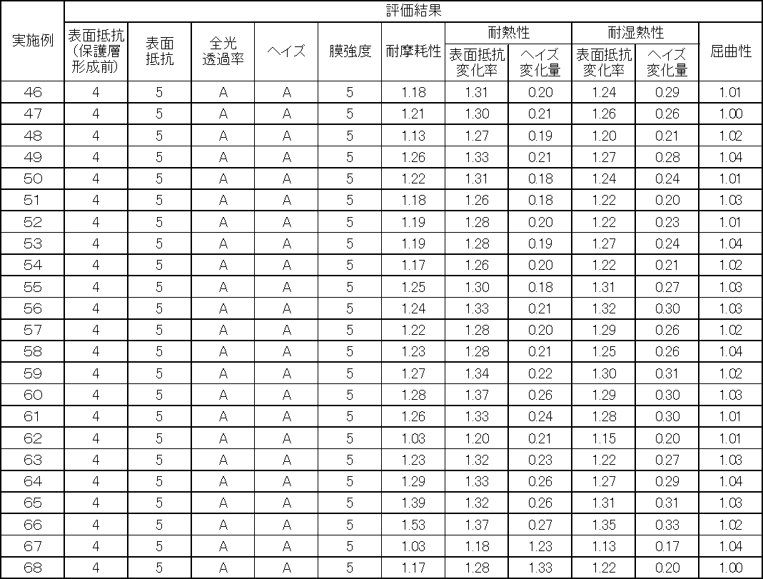
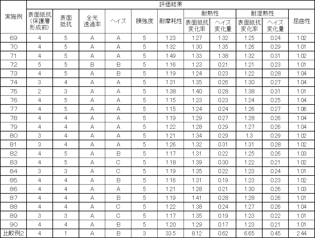
表4および5に示された結果から、本発明に係る導電性部材は導電性と透明性が優れていると共に、耐摩耗性、耐熱性および耐湿熱性に優れると同時に、耐屈曲性に優れていることが理解できる。特に、保護層を設けたことにより、単に膜強度が著しく高まっているだけでなく、表面抵抗率が保護層を設ける前と同等か、又はそれより低い値に改善されるという著しい効果を奏していることが分かる。
(実施例91)
<<導電性層の形成>>
下記組成のアルコキシド化合物の溶液を60℃で1時間撹拌して均一になったことを確認した。得られたアルコキシド化合物溶液3.52部と前記調整例1で得られた銀ナノワイヤー水分散液(1)16.56部を混合し、さらに蒸留水で希釈して銀含有ゾルゲル塗布液を得た。前述のPET基板101の第2の接着層32の表面にコロナ放電処理を施し、その表面にバーコート法で銀量が0.035g/m2、銀含有ゾルゲル塗布液中のゾルゲル成分の固形分塗布量が0.245g/m2となるように上記銀含有ゾルゲル塗布液を塗布したのち、140℃で1分間乾燥してゾルゲル反応を起こさせて、導電性層を形成した。導電性層におけるテトラエトキシシラン/金属ナノワイヤーの質量比は7/1となった。また、導電性層の厚みは0.029μmとなった。
<アルコキシド化合物の溶液>
・テトラエトキシシラン 5.0部
(KBE-04、信越化学工業(株)製)
・1%酢酸水溶液 10.0部
・蒸留水 4.0部
<<導電性層の形成>>
下記組成のアルコキシド化合物の溶液を60℃で1時間撹拌して均一になったことを確認した。得られたアルコキシド化合物溶液3.52部と前記調整例1で得られた銀ナノワイヤー水分散液(1)16.56部を混合し、さらに蒸留水で希釈して銀含有ゾルゲル塗布液を得た。前述のPET基板101の第2の接着層32の表面にコロナ放電処理を施し、その表面にバーコート法で銀量が0.035g/m2、銀含有ゾルゲル塗布液中のゾルゲル成分の固形分塗布量が0.245g/m2となるように上記銀含有ゾルゲル塗布液を塗布したのち、140℃で1分間乾燥してゾルゲル反応を起こさせて、導電性層を形成した。導電性層におけるテトラエトキシシラン/金属ナノワイヤーの質量比は7/1となった。また、導電性層の厚みは0.029μmとなった。
<アルコキシド化合物の溶液>
・テトラエトキシシラン 5.0部
(KBE-04、信越化学工業(株)製)
・1%酢酸水溶液 10.0部
・蒸留水 4.0部
<<保護層の形成>>
実施例1で使用した保護層を形成するためのゾルゲル塗布液と同じものを、固形分塗布量が0.50g/m2となるように導電性層上に塗布したのち、140℃で1分間乾燥し、ゾルゲル反応を起こさせて保護層を形成し、非パターン化導電性層を有する導電性部材を得た。保護層の厚みは、0.13μmであった。
実施例1で使用した保護層を形成するためのゾルゲル塗布液と同じものを、固形分塗布量が0.50g/m2となるように導電性層上に塗布したのち、140℃で1分間乾燥し、ゾルゲル反応を起こさせて保護層を形成し、非パターン化導電性層を有する導電性部材を得た。保護層の厚みは、0.13μmであった。
<<パターニング>>
上記で得られた導電性部材について、以下の方法によりパターニング処理を行った。スクリーン印刷は、ミノグループ社製WHT-3型とスキージNo.4イエローを使用した。パターニングを形成するための銀ナノワイヤーの溶解液はCP-48S-A液と、CP-48S-B液(いずれも、富士フイルム社製)と、純水とを1:1:1となるように混合し、ヒドロキシエチルセルロースで増粘させて形成し、スクリーン印刷用のインクとした。使用したパターンメッシュはストライプパターン(ライン/スペース=50μm/50μm)を用いた。上記パターニング処理を行い、導電性領域と非導電性領域とを含む導電性層を形成した。かくして、実施例91の導電性部材を得た。
上記で得られた導電性部材について、以下の方法によりパターニング処理を行った。スクリーン印刷は、ミノグループ社製WHT-3型とスキージNo.4イエローを使用した。パターニングを形成するための銀ナノワイヤーの溶解液はCP-48S-A液と、CP-48S-B液(いずれも、富士フイルム社製)と、純水とを1:1:1となるように混合し、ヒドロキシエチルセルロースで増粘させて形成し、スクリーン印刷用のインクとした。使用したパターンメッシュはストライプパターン(ライン/スペース=50μm/50μm)を用いた。上記パターニング処理を行い、導電性領域と非導電性領域とを含む導電性層を形成した。かくして、実施例91の導電性部材を得た。
(実施例92~106)
実施例91において、保護層の形成に使用したゾルゲル塗布液に含まれる3-グリシドキシプロピルトリメトキシシランとテトラエトキシシランの両者を、下記に記載した化合物(一つまたは二つ)および量に変更した以外は実施例91と同様にして、実施例92~106の導電性部材を得た。
実施例92:3-グリシドキシプロピルトリメトキシシラン 12.7部
(厚み:0.14μm)
実施例93:テトラエトキシシラン 12.7部
(厚み:0.12μm)
実施例94:3-グリシドキシプロピルトリメトキシシラン 0.6部
テトラエトキシシラン 12.1部
(厚み:0.13μm)
実施例95:3-グリシドキシプロピルトリメトキシシラン 1.3部
テトラエトキシシラン 11.4部
(厚み:0.13μm)
実施例96:3-グリシドキシプロピルトリメトキシシラン 3.8部
テトラエトキシシラン 8.9部
(厚み:0.13μm)
実施例97:3-グリシドキシプロピルトリメトキシシラン 6.35部
テトラエトキシシラン 6.35部
(厚み:0.13μm)
実施例98:3-グリシドキシプロピルトリメトキシシラン 10.2部
テトラエトキシシラン 2.5部
(厚み:0.13μm)
実施例99:3-グリシドキシプロピルトリメトキシシラン 12.5部
テトラエトキシシラン 0.2部
(厚み:0.13μm)
実施例100:テトラプロポキシチタネート 12.7部
(厚み:0.12μm)
実施例101:テトラエトキシジルコネート 12.7部
(厚み:0.12μm)
実施例102:2-(3,4-エポキシシクロヘキシル)エチルトリメトキシシラン
5.9部
テトラメトキシシラン 6.8部
(厚み:0.14μm)
実施例103:ウレイドプロピルトリエトキシシラン 5.9部
テトラエトキシシラン 6.8部
(厚み:0.14μm)
実施例104:ジエチルジメトキシシラン 5.9部
テトラエトキシシラン 6.8部
(厚み:0.13μm)
実施例105:プロピルトリエトキシチタネート 5.9部
テトライソプロポキシチタネート 6.8部
(厚み:0.12μm)
実施例106:エチルトリエトキシジルコネート 5.9部
テトラプロポキシジルコネート 6.8部
(厚み:0.12μm)
実施例91において、保護層の形成に使用したゾルゲル塗布液に含まれる3-グリシドキシプロピルトリメトキシシランとテトラエトキシシランの両者を、下記に記載した化合物(一つまたは二つ)および量に変更した以外は実施例91と同様にして、実施例92~106の導電性部材を得た。
実施例92:3-グリシドキシプロピルトリメトキシシラン 12.7部
(厚み:0.14μm)
実施例93:テトラエトキシシラン 12.7部
(厚み:0.12μm)
実施例94:3-グリシドキシプロピルトリメトキシシラン 0.6部
テトラエトキシシラン 12.1部
(厚み:0.13μm)
実施例95:3-グリシドキシプロピルトリメトキシシラン 1.3部
テトラエトキシシラン 11.4部
(厚み:0.13μm)
実施例96:3-グリシドキシプロピルトリメトキシシラン 3.8部
テトラエトキシシラン 8.9部
(厚み:0.13μm)
実施例97:3-グリシドキシプロピルトリメトキシシラン 6.35部
テトラエトキシシラン 6.35部
(厚み:0.13μm)
実施例98:3-グリシドキシプロピルトリメトキシシラン 10.2部
テトラエトキシシラン 2.5部
(厚み:0.13μm)
実施例99:3-グリシドキシプロピルトリメトキシシラン 12.5部
テトラエトキシシラン 0.2部
(厚み:0.13μm)
実施例100:テトラプロポキシチタネート 12.7部
(厚み:0.12μm)
実施例101:テトラエトキシジルコネート 12.7部
(厚み:0.12μm)
実施例102:2-(3,4-エポキシシクロヘキシル)エチルトリメトキシシラン
5.9部
テトラメトキシシラン 6.8部
(厚み:0.14μm)
実施例103:ウレイドプロピルトリエトキシシラン 5.9部
テトラエトキシシラン 6.8部
(厚み:0.14μm)
実施例104:ジエチルジメトキシシラン 5.9部
テトラエトキシシラン 6.8部
(厚み:0.13μm)
実施例105:プロピルトリエトキシチタネート 5.9部
テトライソプロポキシチタネート 6.8部
(厚み:0.12μm)
実施例106:エチルトリエトキシジルコネート 5.9部
テトラプロポキシジルコネート 6.8部
(厚み:0.12μm)
(実施例107~111)
実施例91において、保護層を形成するためのゾルゲル塗布液の固形分塗布量を下記のように変更した以外は実施例91と同様にして、実施例107~111の導電性部材を得た。各保護層の厚みは、下記のとおりであった。
実施例107:1.00g/m2(厚み:0.250μm)
実施例108:0.35g/m2(厚み:0.092μm)
実施例109:0.15g/m2(厚み:0.040μm)
実施例110:0.10g/m2(厚み:0.026μm)
実施例111:0.05g/m2(厚み:0.013μm)
実施例91において、保護層を形成するためのゾルゲル塗布液の固形分塗布量を下記のように変更した以外は実施例91と同様にして、実施例107~111の導電性部材を得た。各保護層の厚みは、下記のとおりであった。
実施例107:1.00g/m2(厚み:0.250μm)
実施例108:0.35g/m2(厚み:0.092μm)
実施例109:0.15g/m2(厚み:0.040μm)
実施例110:0.10g/m2(厚み:0.026μm)
実施例111:0.05g/m2(厚み:0.013μm)
(実施例112~116)
実施例93において、保護層を形成するためのゾルゲル塗布液の固形分塗布量を下記のように変更した以外は実施例93と同様にして、実施例112~116の導電性部材を得た。各保護層の厚みは、下記のとおりであった。
実施例112:1.00g/m2(厚み:0.245μm)
実施例113:0.35g/m2(厚み:0.090μm)
実施例114:0.15g/m2(厚み:0.039μm)
実施例115:0.10g/m2(厚み:0.025μm)
実施例116:0.05g/m2(厚み:0.013μm)
実施例93において、保護層を形成するためのゾルゲル塗布液の固形分塗布量を下記のように変更した以外は実施例93と同様にして、実施例112~116の導電性部材を得た。各保護層の厚みは、下記のとおりであった。
実施例112:1.00g/m2(厚み:0.245μm)
実施例113:0.35g/m2(厚み:0.090μm)
実施例114:0.15g/m2(厚み:0.039μm)
実施例115:0.10g/m2(厚み:0.025μm)
実施例116:0.05g/m2(厚み:0.013μm)
(実施例117~120)
実施例91で用いた銀含有ゾルゲル塗布液を用いて銀含有ゾルゲル塗布液中のゾルゲル成分(テトラエトキシシラン)の固形分塗布量および銀量を下記のとおりとなるように変更した以外は実施例91と同様にして、実施例117~120の導電性部材を得た。各導電性層の厚みは、下記のとおりであった。
実施例117:ゾルゲル成分の固形分塗布量0.700g/m2、銀量0.100g/m2(厚み:0.185μm)
実施例118:ゾルゲル成分の固形分塗布量0.140g/m2、銀量0.020g/m2(厚み:0.037μm)
実施例119:ゾルゲル成分の固形分塗布量0.070g/m2、銀量0.010g/m2(厚み:0.018μm)
実施例120:ゾルゲル成分の固形分塗布量0.035g/m2、銀量0.005g/m2(厚み:0.009μm)
実施例91で用いた銀含有ゾルゲル塗布液を用いて銀含有ゾルゲル塗布液中のゾルゲル成分(テトラエトキシシラン)の固形分塗布量および銀量を下記のとおりとなるように変更した以外は実施例91と同様にして、実施例117~120の導電性部材を得た。各導電性層の厚みは、下記のとおりであった。
実施例117:ゾルゲル成分の固形分塗布量0.700g/m2、銀量0.100g/m2(厚み:0.185μm)
実施例118:ゾルゲル成分の固形分塗布量0.140g/m2、銀量0.020g/m2(厚み:0.037μm)
実施例119:ゾルゲル成分の固形分塗布量0.070g/m2、銀量0.010g/m2(厚み:0.018μm)
実施例120:ゾルゲル成分の固形分塗布量0.035g/m2、銀量0.005g/m2(厚み:0.009μm)
(実施例121~126)
実施例91で用いた導電性層を形成するための銀含有ゾルゲル塗布液におけるアルコキシド化合物溶液、銀ナノワイヤー水分散液(1)、および、溶媒(蒸留水)の混合比を適宜変更し、銀含有ゾルゲル液中のゾルゲル成分(テトラエトキシシラン)の固形分塗布量および銀量を下記のとおりに変更した以外は実施例91と同様にして、実施例121~126の導電性部材を得た。各導電性層の厚みは、下記のとおりであった。
実施例121:ゾルゲル成分の固形分塗布量0.350g/m2、銀量0.035g/m2(厚み:0.092μm)
実施例122:ゾルゲル成分の固形分塗布量0.280g/m2、銀量0.035g/m2(厚み:0.073μm)
実施例123:ゾルゲル成分の固形分塗布量0.200g/m2、銀量0.020g/m2(厚み:0.052μm)
実施例124:ゾルゲル成分の固形分塗布量0.160g/m2、銀量0.020g/m2(厚み:0.042μm)
実施例125:ゾルゲル成分の固形分塗布量0.150g/m2、銀量0.015g/m2(厚み:0.040μm)
実施例126:ゾルゲル成分の固形分塗布量0.120g/m2、銀量0.015g/m2(厚み:0.032μm)
実施例91で用いた導電性層を形成するための銀含有ゾルゲル塗布液におけるアルコキシド化合物溶液、銀ナノワイヤー水分散液(1)、および、溶媒(蒸留水)の混合比を適宜変更し、銀含有ゾルゲル液中のゾルゲル成分(テトラエトキシシラン)の固形分塗布量および銀量を下記のとおりに変更した以外は実施例91と同様にして、実施例121~126の導電性部材を得た。各導電性層の厚みは、下記のとおりであった。
実施例121:ゾルゲル成分の固形分塗布量0.350g/m2、銀量0.035g/m2(厚み:0.092μm)
実施例122:ゾルゲル成分の固形分塗布量0.280g/m2、銀量0.035g/m2(厚み:0.073μm)
実施例123:ゾルゲル成分の固形分塗布量0.200g/m2、銀量0.020g/m2(厚み:0.052μm)
実施例124:ゾルゲル成分の固形分塗布量0.160g/m2、銀量0.020g/m2(厚み:0.042μm)
実施例125:ゾルゲル成分の固形分塗布量0.150g/m2、銀量0.015g/m2(厚み:0.040μm)
実施例126:ゾルゲル成分の固形分塗布量0.120g/m2、銀量0.015g/m2(厚み:0.032μm)
(実施例127)
実施例91において、PET基板を調製例3で作製したガラス基板に変更した以外は実施例91と同様にして、実施例127の導電性部材を得た。
実施例91において、PET基板を調製例3で作製したガラス基板に変更した以外は実施例91と同様にして、実施例127の導電性部材を得た。
(実施例128~135)
実施例91にて使用した導電性層を形成するための銀含有ゾルゲル塗布液における銀ナノワイヤー水分散液(1)を、銀ナノワイヤーの平均長軸長および平均短軸長が下記表6に示される銀ナノワイヤー水分散液(2)~(9)に変更した以外は91と同様にして、実施例128~135の導電性部材を得た。
実施例91にて使用した導電性層を形成するための銀含有ゾルゲル塗布液における銀ナノワイヤー水分散液(1)を、銀ナノワイヤーの平均長軸長および平均短軸長が下記表6に示される銀ナノワイヤー水分散液(2)~(9)に変更した以外は91と同様にして、実施例128~135の導電性部材を得た。
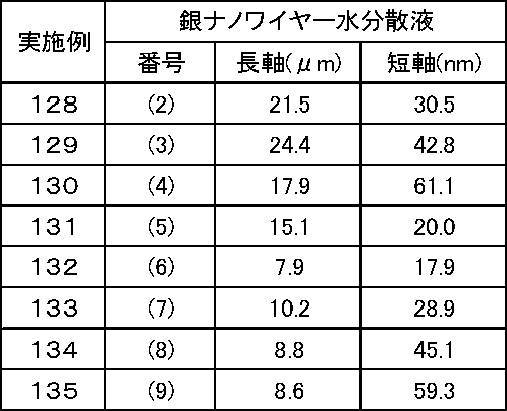
<<評価>>
各導電性部材について、前述と同じ方法で表面抵抗率、光学特性(全光透過率、ヘイズ)、膜強度、耐摩耗性、耐熱性、耐湿熱性および屈曲性を評価した。結果を表7および8に示す。
なお、表7および8には、参考データとして、各導電性部材にける保護層形成前の表面抵抗率についての評価ランクも記載した。
各導電性部材について、前述と同じ方法で表面抵抗率、光学特性(全光透過率、ヘイズ)、膜強度、耐摩耗性、耐熱性、耐湿熱性および屈曲性を評価した。結果を表7および8に示す。
なお、表7および8には、参考データとして、各導電性部材にける保護層形成前の表面抵抗率についての評価ランクも記載した。


表7および8に示された結果から、本発明に係る導電性部材は導電性と透明性が優れていると共に、耐摩耗性、耐熱性および耐湿熱性に優れると同時に、耐屈曲性に優れていることが理解できる。特に、保護層を設けたことにより、単に膜強度が著しく高まっているだけでなく、表面抵抗率が保護層を設ける前と同等か、又はそれより低い値に改善されるという著しい効果を奏していることが分かる。
(実施例136~139)
実施例109において保護層を形成するためのゾルゲル塗布液を下記条件で調整した以外は実施例109と同様にして実施例136~139の導電性部材を得た。各保護層の厚みは、下記のとおりであった。ゾルゲル塗布液中に含まれるアルコキシド化合物の部分縮合物の重量平均分子量(Mw)をGPC(ポリスチレン換算)で測定した。
実施例109:60℃1.0時間攪拌 厚み:0.040μm Mw:3,500
実施例136:60℃1.5時間攪拌 厚み:0.042μm Mw:9,600
実施例137:60℃2.0時間攪拌 厚み:0.043μm Mw:19,000
実施例138:60℃2.5時間攪拌 厚み:0.044μm Mw:37,000
実施例139:60℃3.0時間攪拌 厚み:0.046μm Mw:70,000
実施例109において保護層を形成するためのゾルゲル塗布液を下記条件で調整した以外は実施例109と同様にして実施例136~139の導電性部材を得た。各保護層の厚みは、下記のとおりであった。ゾルゲル塗布液中に含まれるアルコキシド化合物の部分縮合物の重量平均分子量(Mw)をGPC(ポリスチレン換算)で測定した。
実施例109:60℃1.0時間攪拌 厚み:0.040μm Mw:3,500
実施例136:60℃1.5時間攪拌 厚み:0.042μm Mw:9,600
実施例137:60℃2.0時間攪拌 厚み:0.043μm Mw:19,000
実施例138:60℃2.5時間攪拌 厚み:0.044μm Mw:37,000
実施例139:60℃3.0時間攪拌 厚み:0.046μm Mw:70,000
(実施例140~143)
実施例114において保護層を形成するためのゾルゲル塗布液を下記条件で調整した以外は実施例109と同様にして実施例140~143の導電性部材を得た。各保護層の厚み、ゾルゲル塗布液中に含まれるアルコキシド化合物の部分縮合物の重量平均分子量(Mw)は下記のとおりであった。
実施例114:60℃1.0時間攪拌 厚み:0.039μm Mw:4,400
実施例140:60℃1.5時間攪拌 厚み:0.040μm Mw:12,000
実施例141:60℃2.0時間攪拌 厚み:0.041μm Mw:24,000
実施例142:60℃2.5時間攪拌 厚み:0.042μm Mw:46,000
実施例143:60℃3.0時間攪拌 厚み:0.044μm Mw:87,000
実施例114において保護層を形成するためのゾルゲル塗布液を下記条件で調整した以外は実施例109と同様にして実施例140~143の導電性部材を得た。各保護層の厚み、ゾルゲル塗布液中に含まれるアルコキシド化合物の部分縮合物の重量平均分子量(Mw)は下記のとおりであった。
実施例114:60℃1.0時間攪拌 厚み:0.039μm Mw:4,400
実施例140:60℃1.5時間攪拌 厚み:0.040μm Mw:12,000
実施例141:60℃2.0時間攪拌 厚み:0.041μm Mw:24,000
実施例142:60℃2.5時間攪拌 厚み:0.042μm Mw:46,000
実施例143:60℃3.0時間攪拌 厚み:0.044μm Mw:87,000
<<評価>>
各導電性部材について、前述と同じ方法で表面抵抗率、光学特性(全光透過率、ヘイズ)、膜強度、耐摩耗性、耐熱性、耐湿熱性および屈曲性を評価し、下記方法でエッチング性を評価した。
<エッチング性>
得られた導電性部材を下記組成のエッチング液(液温25℃)に、浸漬時間を30秒間から180秒間に変化させて浸漬し、その後流水で洗浄し、乾燥した。表面抵抗率を三菱化学社製Loresta-GP MCP-T600を用いて、ヘイズをガードナー社製ヘイズガードプラスを用いて測定した。エッチング液浸漬後に表面抵抗率が高く、かつΔヘイズ(浸漬前後のヘイズ差)が大きいほどエッチング性に優れる。上記エッチング液に25℃で浸漬したときに、前記表面抵抗率が108Ω/□となり、かつ、前記エッチング液に浸漬する前のヘイズから浸漬した後のヘイズを減じたヘイズ差が0.4%となるまでに要する時間(浸漬時間)を求め、下記のランク付けを行った。
〔エッチング液の組成〕:下記の各成分を含有する水溶液。
・エチレンジアミン四酢酸鉄アンモニウム・・・ 2.5質量%
・チオ硫酸アンモニウム・・・ 7.5質量%
・亜硫酸アンモニウム・・・ 2.5質量%
・重亜硫酸アンモニウム・・・ 2.5質量%
・水・・・ 85.0質量%
ランク5:表面抵抗率1.0×10⁸Ω/□以上、およびΔヘイズ0.4%以上となるまでのエッチング液浸漬時間が30秒以内で極めて優秀なレベル
ランク4:同上時間が、30秒以上~60秒以内で優秀なレベル
ランク3:同上時間が、60秒以上~120秒以内で良好なレベル
ランク2:同上時間が、120秒以上~180秒以内で実用上問題があるレベル
ランク1:同上時間が、180秒以上であり、実用上極めて問題があるレベル
結果を表9に示す。
なお、表9には、参考データとして、各導電性部材にける保護層形成前の表面抵抗率についての評価ランクも記載した。
各導電性部材について、前述と同じ方法で表面抵抗率、光学特性(全光透過率、ヘイズ)、膜強度、耐摩耗性、耐熱性、耐湿熱性および屈曲性を評価し、下記方法でエッチング性を評価した。
<エッチング性>
得られた導電性部材を下記組成のエッチング液(液温25℃)に、浸漬時間を30秒間から180秒間に変化させて浸漬し、その後流水で洗浄し、乾燥した。表面抵抗率を三菱化学社製Loresta-GP MCP-T600を用いて、ヘイズをガードナー社製ヘイズガードプラスを用いて測定した。エッチング液浸漬後に表面抵抗率が高く、かつΔヘイズ(浸漬前後のヘイズ差)が大きいほどエッチング性に優れる。上記エッチング液に25℃で浸漬したときに、前記表面抵抗率が108Ω/□となり、かつ、前記エッチング液に浸漬する前のヘイズから浸漬した後のヘイズを減じたヘイズ差が0.4%となるまでに要する時間(浸漬時間)を求め、下記のランク付けを行った。
〔エッチング液の組成〕:下記の各成分を含有する水溶液。
・エチレンジアミン四酢酸鉄アンモニウム・・・ 2.5質量%
・チオ硫酸アンモニウム・・・ 7.5質量%
・亜硫酸アンモニウム・・・ 2.5質量%
・重亜硫酸アンモニウム・・・ 2.5質量%
・水・・・ 85.0質量%
ランク5:表面抵抗率1.0×10⁸Ω/□以上、およびΔヘイズ0.4%以上となるまでのエッチング液浸漬時間が30秒以内で極めて優秀なレベル
ランク4:同上時間が、30秒以上~60秒以内で優秀なレベル
ランク3:同上時間が、60秒以上~120秒以内で良好なレベル
ランク2:同上時間が、120秒以上~180秒以内で実用上問題があるレベル
ランク1:同上時間が、180秒以上であり、実用上極めて問題があるレベル
結果を表9に示す。
なお、表9には、参考データとして、各導電性部材にける保護層形成前の表面抵抗率についての評価ランクも記載した。
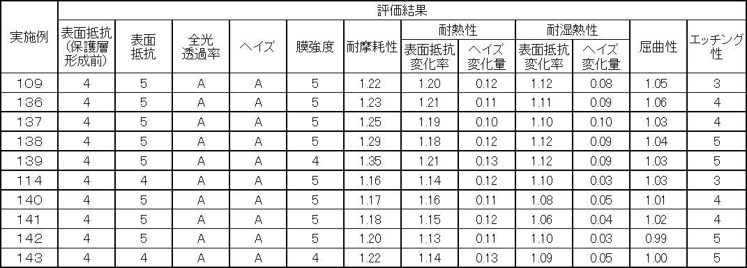
(実施例144の作製)
実施例91において、銀ナノワイヤー水分散液(1)を米国特許公開2011/0174190A1号明細書の段落0151~段落0160に記載の実施例1および2に従って調製した銀ナノワイヤー分散液を蒸留水にて0.85%に希釈した銀ナノワイヤー水分散液(10)を用いた以外は実施例91と同様にして導電性部材144を得た。
実施例91において、銀ナノワイヤー水分散液(1)を米国特許公開2011/0174190A1号明細書の段落0151~段落0160に記載の実施例1および2に従って調製した銀ナノワイヤー分散液を蒸留水にて0.85%に希釈した銀ナノワイヤー水分散液(10)を用いた以外は実施例91と同様にして導電性部材144を得た。
(実施例145~154の作製)
下記導電性部材の銀ナノワイヤー水分散液(1)を上記銀ナノワイヤー水分散液(10)に変更した以外は同様にして実施例145~154を得た。
実施例145:実施例93
実施例146:実施例96
実施例147:実施例98
実施例148:実施例109
実施例149:実施例114
実施例150:実施例118
実施例151:実施例123
実施例152:実施例124
実施例153:実施例125
実施例154:実施例126
下記導電性部材の銀ナノワイヤー水分散液(1)を上記銀ナノワイヤー水分散液(10)に変更した以外は同様にして実施例145~154を得た。
実施例145:実施例93
実施例146:実施例96
実施例147:実施例98
実施例148:実施例109
実施例149:実施例114
実施例150:実施例118
実施例151:実施例123
実施例152:実施例124
実施例153:実施例125
実施例154:実施例126
<<評価>>
得られた各導電性部材について、前述と同じ方法で表面抵抗率、光学特性(全光透過率、ヘイズ)、膜強度、耐磨耗性、耐熱性、耐湿熱性、屈曲性を評価した。結果を表10に示す。
得られた各導電性部材について、前述と同じ方法で表面抵抗率、光学特性(全光透過率、ヘイズ)、膜強度、耐磨耗性、耐熱性、耐湿熱性、屈曲性を評価した。結果を表10に示す。

表10に示された結果から、米国特許US2011/0174190A1号公報に記載の銀ナノワイヤーを使用した導電性部材についても、全光透過率、ヘイズ、膜強度および耐磨耗性に優れた性能を有していることが分かる。
(実施例155)
実施例91においてアルコキシド化合物の溶液11.71部と銀ナノワイヤー水分散液(1)18.29部を混合した液を用いて保護層を形成した以外は実施例91と同様に導電性部材を得た。保護層の厚みは、0.12μmであった。
実施例91においてアルコキシド化合物の溶液11.71部と銀ナノワイヤー水分散液(1)18.29部を混合した液を用いて保護層を形成した以外は実施例91と同様に導電性部材を得た。保護層の厚みは、0.12μmであった。
(実施例156、157)
実施例155においてアルコキシド化合物の溶液と銀ナノワイヤー水分散液(1)の混合量を下記に変更した以外は実施例155と同様に導電性部材を得た。
実施例156:アルコキシド化合物の溶液 14.69部
銀ナノワイヤー水分散液(1) 15.31部
(厚み:0.13μm)
実施例157:アルコキシド化合物の溶液 18.46部
銀ナノワイヤー水分散液(1) 11.54部
(厚み:0.12μm)
実施例155においてアルコキシド化合物の溶液と銀ナノワイヤー水分散液(1)の混合量を下記に変更した以外は実施例155と同様に導電性部材を得た。
実施例156:アルコキシド化合物の溶液 14.69部
銀ナノワイヤー水分散液(1) 15.31部
(厚み:0.13μm)
実施例157:アルコキシド化合物の溶液 18.46部
銀ナノワイヤー水分散液(1) 11.54部
(厚み:0.12μm)
<<評価>>
得られた各導電性部材について、前述と同じ方法で表面抵抗率、光学特性(全光透過率、ヘイズ)、膜強度、耐磨耗性、耐熱性、耐湿熱性、屈曲性を評価した。結果を表11に示す。
得られた各導電性部材について、前述と同じ方法で表面抵抗率、光学特性(全光透過率、ヘイズ)、膜強度、耐磨耗性、耐熱性、耐湿熱性、屈曲性を評価した。結果を表11に示す。

(実施例158)
<集積型太陽電池の作製>
-アモルファス太陽電池(スーパーストレート型)の作製-
ガラス基板上に、実施例1と同様にして導電性層、保護層を形成し、導電性部材を作製した。但し、導電性層はパターニング処理は行わず全面均一な透明導電性層とした。その上部にプラズマCVD法により膜厚約15nmのp型、膜厚約350nmのi型、および、膜厚約30nmのn型アモルファスシリコンを形成し、裏面反射電極としてガリウム添加酸化亜鉛層20nm、銀層200nmを形成し、光電変換素子101を作製した。
<集積型太陽電池の作製>
-アモルファス太陽電池(スーパーストレート型)の作製-
ガラス基板上に、実施例1と同様にして導電性層、保護層を形成し、導電性部材を作製した。但し、導電性層はパターニング処理は行わず全面均一な透明導電性層とした。その上部にプラズマCVD法により膜厚約15nmのp型、膜厚約350nmのi型、および、膜厚約30nmのn型アモルファスシリコンを形成し、裏面反射電極としてガリウム添加酸化亜鉛層20nm、銀層200nmを形成し、光電変換素子101を作製した。
<CIGS太陽電池(サブストレート型)の作製>
ソーダライムガラス基板上に、直流マグネトロンスパッタ法により膜厚500nm程度のモリブデン電極、真空蒸着法により膜厚約2.5μmのカルコパイライト系半導体材料であるCu(In0.6Ga0.4)Se2薄膜、および、溶液析出法により膜厚約50nmの硫化カドミニウム薄膜、を形成した。
その上に実施例1の導電性層、保護層を形成し、ガラス基板上に透明導電膜を形成し、光電変換素子201を作製した。
各太陽電池について、AM1.5、100mW/cm2の疑似太陽光を照射することで光電変換効率を測定した。その結果、光電変換素子101は10%の変換効率を、そして光電変換素子201は9%の変換効率を示した。
いずれの集積型太陽電池方式においても高い変換効率が得られることが分かった。
ソーダライムガラス基板上に、直流マグネトロンスパッタ法により膜厚500nm程度のモリブデン電極、真空蒸着法により膜厚約2.5μmのカルコパイライト系半導体材料であるCu(In0.6Ga0.4)Se2薄膜、および、溶液析出法により膜厚約50nmの硫化カドミニウム薄膜、を形成した。
その上に実施例1の導電性層、保護層を形成し、ガラス基板上に透明導電膜を形成し、光電変換素子201を作製した。
各太陽電池について、AM1.5、100mW/cm2の疑似太陽光を照射することで光電変換効率を測定した。その結果、光電変換素子101は10%の変換効率を、そして光電変換素子201は9%の変換効率を示した。
いずれの集積型太陽電池方式においても高い変換効率が得られることが分かった。
(実施例159)
-タッチパネルの作製-
実施例1の導電性層、保護層を形成し、ガラス基板上に透明導電膜を形成した。得られた透明導電膜を用いて、『最新タッチパネル技術』(2009年7月6日発行、株式会社テクノタイムズ)、三谷雄二監修、“タッチパネルの技術と開発”、シーエムシー出版(2004年12月発行)、「FPD International 2009 Forum T-11講演テキストブック」、「Cypress Semiconductor Corporation アプリケーションノートAN2292」等に記載の方法により、タッチパネルを作製した。
作製したタッチパネルを使用した場合、光透過率の向上により視認性に優れ、かつ導電性の向上により素手、手袋を嵌めた手、指示具のうち少なくとも一つによる文字等の入力又は画面操作に対し応答性に優れるタッチパネルを製作できることが分かった。
-タッチパネルの作製-
実施例1の導電性層、保護層を形成し、ガラス基板上に透明導電膜を形成した。得られた透明導電膜を用いて、『最新タッチパネル技術』(2009年7月6日発行、株式会社テクノタイムズ)、三谷雄二監修、“タッチパネルの技術と開発”、シーエムシー出版(2004年12月発行)、「FPD International 2009 Forum T-11講演テキストブック」、「Cypress Semiconductor Corporation アプリケーションノートAN2292」等に記載の方法により、タッチパネルを作製した。
作製したタッチパネルを使用した場合、光透過率の向上により視認性に優れ、かつ導電性の向上により素手、手袋を嵌めた手、指示具のうち少なくとも一つによる文字等の入力又は画面操作に対し応答性に優れるタッチパネルを製作できることが分かった。
本発明の具体的態様の前記記述は、記述と説明の目的で提供するものである。開示された、まさにその形態に本発明を限定することを企図するものでもなく、或いは網羅的なものを企図するものでもない。明らかに、当業者が多くの修飾や変形をすることができることは自明である。該態様は、本発明の概念やその実際の応用を最もよく説明するために選定されたものであって、それによって、当業者の他者が企図する特定の用途に適合させるべく種々の態様や種々の変形をなすことができるように、当業者の他者に本発明を理解せしめるためのものである。
2011年4月14日出願の日本特許出願第2011-090346号公報、2011年11月30日出願の日本特許出願第2011-263073号公報、並びに2012年3月23日出願の日本特許出願第2012-068214号公報は、その開示全体がここに参照文献として組み込まれるものである。
本明細書に記述された全ての刊行物や特許出願、並びに技術標準は、それら個々の刊行物や特許出願、並びに技術標準が引用文献として特別に、そして個々に組み込むことが指定されている場合には、該引用文献と同じ限定範囲においてここに組み込まれるものである。本発明の範囲は下記特許請求の範囲及びその等価物に拠って決定されることを企図するものである。
本明細書に記述された全ての刊行物や特許出願、並びに技術標準は、それら個々の刊行物や特許出願、並びに技術標準が引用文献として特別に、そして個々に組み込むことが指定されている場合には、該引用文献と同じ限定範囲においてここに組み込まれるものである。本発明の範囲は下記特許請求の範囲及びその等価物に拠って決定されることを企図するものである。
Claims (23)
- 基材上に、平均短軸長が150nm以下の金属ナノワイヤーおよびマトリックスを含む導電性層、並びに、下記一般式(I)で示される三次元架橋構造を含んで構成される保護層を、この順に備え、前記保護層上から測定した表面抵抗率が、1,000Ω/□以下である導電性部材。
-M1-O-M1- (I)
(一般式(I)中、M1はSi、Ti、ZrおよびAlからなる群より選ばれた元素を示す。) - 前記マトリックスが、光重合性組成物の光硬化物またはSi、Ti、ZrおよびAlからなる群より選ばれた元素のアルコキシド化合物の少なくとも一つを加水分解および重縮合して得られるゾルゲル硬化物である請求項1に記載の導電性部材。
- 前記保護層が、Si、Ti、ZrおよびAlからなる群より選ばれた元素のアルコキシド化合物の少なくとも一つを加水分解および重縮合して得られるゾルゲル硬化物を含む請求項1または請求項2に記載の導電性部材。
- 前記保護層における前記アルコキシド化合物が、下記一般式(II)で示される化合物および下記一般式(III)で示される化合物からなる群より選ばれた少なくとも一つを含む請求項3に記載の導電性部材。
M2(OR1)4 (II)
(一般式(II)中、M2はSi、TiおよびZrからなる群より選ばれた元素を示し、R1はそれぞれ独立に水素原子または炭化水素基を示す。)
M3(OR2)aR3 4-a (III)
(一般式(III)中、M3はSi、TiおよびZrからなる群より選ばれた元素を示し、R2およびR3はそれぞれ独立に水素原子または炭化水素基を示し、aは1~3の整数を示す。) - 前記保護層における前記アルコキシド化合物が、(i)前記一般式(II)で示される化合物から選ばれた少なくとも一つと、(ii)前記一般式(III)で示される化合物から選ばれた少なくとも一つと、を含む請求項4に記載の導電性部材。
- 前記化合物(ii)/前記化合物(i)の質量比が、0.01/1~100/1の範囲にある請求項5に記載の導電性部材。
- 前記一般式(II)中のM2および前記一般式(III)中のM3が、いずれもSiである請求項4~請求項6のいずれか一項に記載の導電性部材。
- 前記金属ナノワイヤーが、銀ナノワイヤーである請求項1~請求項7のいずれか一項に記載の導電性部材。
- 下記組成を有する温度が25℃のエッチング液に120秒間浸漬したとき、浸漬後の前記表面抵抗率が108Ω/□以上であり、浸漬前のヘイズから浸漬後のヘイズを減じたヘイズ差が0.4%以上であり、かつ、浸漬後において前記保護層が除去されていない請求項1~請求項8のいずれか一項に記載の導電性部材。
エッチング液の組成:エチレンジアミン四酢酸鉄アンモニウム2.5質量%、チオ硫酸アンモニウム7.5質量%、亜硫酸アンモニウム2.5質量%および重亜硫酸アンモニウム2.5質量%を含有する水溶液。
- 前記導電性層が、導電性領域および非導電性領域を含んで構成され、少なくとも前記導電性領域が前記金属ナノワイヤーを含む請求項1~請求項9のいずれか一項に記載の導電性部材。
- 前記保護層の表面を、連続加重引掻試験機を使用し、ガーゼを用いて20mm×20mmのサイズで500g荷重で50往復擦る磨耗処理を行ったとき、前記摩耗処理後の導電性層の表面抵抗率(Ω/□)/前記摩耗処理前の導電性層の表面抵抗率(Ω/□)の比が100以下である請求項1~請求項10のいずれか一項に記載の導電性部材。
- 前記導電性部材を、円筒形マンドレル屈曲試験器を用いて直径10mmの円筒マンドレルに20回曲げる屈曲処理を行ったとき、前記屈曲処理後の導電性層の表面抵抗率(Ω/□)/前記屈曲処理前の導電性層の表面抵抗率(Ω/□)の比が2.0以下である請求項1~請求項11のいずれか一項に記載の導電性部材。
- (a)基材上に、平均短軸長が150nm以下の金属ナノワイヤーおよびマトリックスを含む導電性層を形成すること、
(b)前記導電性層上に、Si、Ti、ZrおよびAlからなる群より選ばれた元素のアルコキシド化合物の少なくとも一つを加水分解および重縮合させて得られた部分縮合物を含む水溶液を塗布して、当該水溶液の液膜を導電性層上に形成すること、並びに、
(c)前記水溶液の液膜中のアルコキシド化合物を加水分解および重縮合させて、前記一般式(I)で示される三次元架橋構造を含んで構成される保護層を形成すること、
を含む請求項1に記載の導電性部材の製造方法。 - 前記(c)の後に、さらに前記保護層を加熱して乾燥すること、を含む請求項13に記載の導電性部材の製造方法。
- 前記マトリックスが、光重合性組成物の光硬化物またはSi、Ti、ZrおよびAlからなる群より選ばれた元素のアルコキシド化合物の少なくとも一つを加水分解および重縮合して得られるゾルゲル硬化物である請求項13または請求項14に記載の導電性部材の製造方法。
- 前記(b)におけるアルコキシド化合物が、下記一般式(II)で示される化合物および下記一般式(III)で示される化合物からなる群より選ばれた少なくとも一つを含む請求項13~請求項15のいずれか一項に記載の導電性部材の製造方法。
M2(OR1)4 (II)
(一般式(II)中、M2はSi、TiおよびZrからなる群より選ばれた元素を示し、R1はそれぞれ独立に水素原子または炭化水素基を示す。)
M3(OR2)aR3 4-a (III)
(一般式(III)中、M3はSi、TiおよびZrからなる群より選ばれた元素を示し、R2およびR3はそれぞれ独立に水素原子または炭化水素基を示し、aは1~3の整数を示す。) - 前記(b)におけるアルコキシド化合物が、(i)前記一般式(II)で示される化合物から選ばれた少なくとも一つと、(ii)前記一般式(III)で示される化合物から選ばれた少なくとも一つの化合物と、を含む請求項16に記載の導電性部材の製造方法。
- 前記化合物(ii)/前記化合物(i)の質量比が、0.01/1~100/1の範囲にある請求項17に記載の導電性部材の製造方法。
- 前記一般式(II)中のM2および前記一般式(III)中のM3が、いずれもSiである請求項16~請求項18のいずれか一項に記載の導電性部材の製造方法。
- 前記部分縮合物の重量平均分子量が4,000~90、000の範囲である請求項13~請求項19のいずれか一項に記載の導電性部材の製造方法。
- 前記(a)と(b)の間に、さらに前記導電性層に、導電性領域および非導電性領域を形成することを含む請求項13~請求項20のいずれか一項に記載の導電性部材の製造方法。
- 請求項1~請求項12のいずれか一項に記載の導電性部材を含むタッチパネル。
- 請求項1~請求項12のいずれか一項に記載の導電性部材を含む太陽電池。
Priority Applications (3)
| Application Number | Priority Date | Filing Date | Title |
|---|---|---|---|
| CN201280017608.4A CN103493147A (zh) | 2011-04-14 | 2012-04-04 | 导电性构件、导电性构件的制造方法、触摸屏及太阳电池 |
| KR1020137026962A KR20140016331A (ko) | 2011-04-14 | 2012-04-04 | 도전성 부재, 도전성 부재의 제조 방법, 터치 패널 및 태양 전지 |
| US14/049,379 US20140034360A1 (en) | 2011-04-14 | 2013-10-09 | Conductive member, production method of the same, touch panel, and solar cell |
Applications Claiming Priority (6)
| Application Number | Priority Date | Filing Date | Title |
|---|---|---|---|
| JP2011090346 | 2011-04-14 | ||
| JP2011-090346 | 2011-04-14 | ||
| JP2011-263073 | 2011-11-30 | ||
| JP2011263073 | 2011-11-30 | ||
| JP2012-068214 | 2012-03-23 | ||
| JP2012068214A JP2013137982A (ja) | 2011-04-14 | 2012-03-23 | 導電性部材、導電性部材の製造方法、タッチパネルおよび太陽電池 |
Related Child Applications (1)
| Application Number | Title | Priority Date | Filing Date |
|---|---|---|---|
| US14/049,379 Continuation US20140034360A1 (en) | 2011-04-14 | 2013-10-09 | Conductive member, production method of the same, touch panel, and solar cell |
Publications (1)
| Publication Number | Publication Date |
|---|---|
| WO2012141058A1 true WO2012141058A1 (ja) | 2012-10-18 |
Family
ID=47009236
Family Applications (1)
| Application Number | Title | Priority Date | Filing Date |
|---|---|---|---|
| PCT/JP2012/059266 Ceased WO2012141058A1 (ja) | 2011-04-14 | 2012-04-04 | 導電性部材、導電性部材の製造方法、タッチパネルおよび太陽電池 |
Country Status (6)
| Country | Link |
|---|---|
| US (1) | US20140034360A1 (ja) |
| JP (1) | JP2013137982A (ja) |
| KR (1) | KR20140016331A (ja) |
| CN (1) | CN103493147A (ja) |
| TW (1) | TW201303906A (ja) |
| WO (1) | WO2012141058A1 (ja) |
Cited By (7)
| Publication number | Priority date | Publication date | Assignee | Title |
|---|---|---|---|---|
| WO2014133688A1 (en) * | 2013-01-22 | 2014-09-04 | Cambrios Technologies Corporation | Two-sided laser patterning on thin film substrates |
| US20150140320A1 (en) * | 2013-11-18 | 2015-05-21 | Xerox Corporation | Surface layer and fuser member |
| US9965124B2 (en) | 2013-08-05 | 2018-05-08 | Alps Electric Co., Ltd. | Light transmitting electrically conductive member and method for patterning the same |
| WO2018101334A1 (ja) * | 2016-12-01 | 2018-06-07 | 昭和電工株式会社 | 透明導電基板及びその製造方法 |
| US10465093B2 (en) | 2014-02-24 | 2019-11-05 | Xerox Corporation | Surface layer and fuser member |
| CN112562887A (zh) * | 2020-11-18 | 2021-03-26 | 深圳市华科创智技术有限公司 | 一种耐弯曲性能优异的纳米银线透明导电膜 |
| CN114311899A (zh) * | 2015-04-06 | 2022-04-12 | 大日本印刷株式会社 | 导电性层叠体、触控面板和导电性层叠体的制造方法 |
Families Citing this family (20)
| Publication number | Priority date | Publication date | Assignee | Title |
|---|---|---|---|---|
| CN104160456B (zh) * | 2012-03-02 | 2016-10-26 | 独立行政法人科学技术振兴机构 | 导电性膜的形成方法 |
| WO2014157856A1 (ko) * | 2013-03-25 | 2014-10-02 | 전자부품연구원 | 감광성 코팅 조성물, 그를 이용한 코팅 전도막 및 그의 제조 방법 |
| CN105244081B (zh) | 2013-10-16 | 2019-03-26 | 日立化成株式会社 | 劣化抑制方法、膜及其制造方法以及层叠体 |
| DE102014005339B4 (de) * | 2014-01-28 | 2022-06-09 | Wolfgang B. Thörner | Verfahren zur Herstellung eines Kontaktelements |
| TW201543977A (zh) * | 2014-05-07 | 2015-11-16 | Daxin Materials Corp | 形成含銀之導電圖案層的方法 |
| KR101896976B1 (ko) * | 2014-07-15 | 2018-10-04 | 후지필름 가부시키가이샤 | 적층 재료의 제조 방법, 적층 재료, 투명 적층체의 제조 방법, 투명 적층체, 정전 용량형 입력 장치 및 화상 표시 장치 |
| JP6499661B2 (ja) * | 2014-07-31 | 2019-04-10 | 富士フイルム株式会社 | 窓用断熱フィルム、窓用断熱ガラスおよび窓 |
| CN107107455B (zh) * | 2014-11-13 | 2019-07-05 | 富士胶片株式会社 | 导电体的成型方法及导电体 |
| KR102375889B1 (ko) | 2014-12-19 | 2022-03-16 | 삼성전자주식회사 | 에너지 발생 장치 및 그 제조방법 |
| KR102681839B1 (ko) * | 2015-04-06 | 2024-07-04 | 다이니폰 인사츠 가부시키가이샤 | 도전성 적층체, 터치 패널 및 도전성 적층체의 제조 방법 |
| WO2017059573A1 (en) * | 2015-10-09 | 2017-04-13 | Shenzhen Xpectvision Technology Co., Ltd. | Packaging methods of semiconductor x-ray detectors |
| CN108136803B (zh) * | 2015-11-13 | 2021-04-23 | 埃克阿泰克有限责任公司 | 导电浆料及印刷其的方法 |
| JP6863715B2 (ja) * | 2015-12-25 | 2021-04-21 | トッパン・フォームズ株式会社 | 積層体及び積層体の製造方法 |
| JP6803723B2 (ja) * | 2015-12-25 | 2020-12-23 | トッパン・フォームズ株式会社 | 積層体 |
| WO2017110787A1 (ja) * | 2015-12-25 | 2017-06-29 | トッパン・フォームズ株式会社 | 積層体及び積層体の製造方法 |
| JP7015198B2 (ja) * | 2017-03-29 | 2022-02-02 | トッパン・フォームズ株式会社 | 積層体 |
| KR102185171B1 (ko) * | 2018-12-04 | 2020-12-01 | 주식회사 디케이티 | 투명전극 디바이스 |
| CN113396053A (zh) * | 2019-02-18 | 2021-09-14 | 昭和电工株式会社 | 透明导电基体及包含该透明导电基体的触摸面板 |
| KR102581214B1 (ko) * | 2019-04-03 | 2023-09-21 | 캄브리오스 필름 솔루션스 코포레이션 | 전기 전도성 필름 |
| TWI872836B (zh) * | 2023-11-30 | 2025-02-11 | 凱新全球科技股份有限公司 | 保護膠及製造無縫顯示單元的方法 |
Citations (5)
| Publication number | Priority date | Publication date | Assignee | Title |
|---|---|---|---|---|
| JPS61183810A (ja) * | 1985-02-07 | 1986-08-16 | 三井東圧化学株式会社 | 透明電極 |
| JPH08127097A (ja) * | 1994-11-01 | 1996-05-21 | Mitsui Toatsu Chem Inc | 透明導電性フィルム |
| WO2009063744A1 (ja) * | 2007-11-16 | 2009-05-22 | Konica Minolta Holdings, Inc. | 金属ナノワイヤの製造方法、金属ナノワイヤ及び透明導電体 |
| JP2009215594A (ja) * | 2008-03-10 | 2009-09-24 | Fujifilm Corp | 金属ナノワイヤー及びその製造方法、並びに水性分散物及び透明導電体 |
| JP2010103109A (ja) * | 2009-10-08 | 2010-05-06 | Jgc Catalysts & Chemicals Ltd | 透明導電性被膜形成用塗布液、透明導電性被膜付基材および表示装置 |
Family Cites Families (2)
| Publication number | Priority date | Publication date | Assignee | Title |
|---|---|---|---|---|
| ATE532217T1 (de) * | 2005-08-12 | 2011-11-15 | Cambrios Technologies Corp | Verfahren zur herstellung von transparente leiter auf nanodrahtbasis |
| JP2008103622A (ja) * | 2006-10-20 | 2008-05-01 | Fujifilm Corp | プリント配線板作製用積層体及びそれを用いたプリント配線板の作製方法 |
-
2012
- 2012-03-23 JP JP2012068214A patent/JP2013137982A/ja not_active Abandoned
- 2012-04-04 CN CN201280017608.4A patent/CN103493147A/zh active Pending
- 2012-04-04 WO PCT/JP2012/059266 patent/WO2012141058A1/ja not_active Ceased
- 2012-04-04 KR KR1020137026962A patent/KR20140016331A/ko not_active Withdrawn
- 2012-04-12 TW TW101112904A patent/TW201303906A/zh unknown
-
2013
- 2013-10-09 US US14/049,379 patent/US20140034360A1/en not_active Abandoned
Patent Citations (5)
| Publication number | Priority date | Publication date | Assignee | Title |
|---|---|---|---|---|
| JPS61183810A (ja) * | 1985-02-07 | 1986-08-16 | 三井東圧化学株式会社 | 透明電極 |
| JPH08127097A (ja) * | 1994-11-01 | 1996-05-21 | Mitsui Toatsu Chem Inc | 透明導電性フィルム |
| WO2009063744A1 (ja) * | 2007-11-16 | 2009-05-22 | Konica Minolta Holdings, Inc. | 金属ナノワイヤの製造方法、金属ナノワイヤ及び透明導電体 |
| JP2009215594A (ja) * | 2008-03-10 | 2009-09-24 | Fujifilm Corp | 金属ナノワイヤー及びその製造方法、並びに水性分散物及び透明導電体 |
| JP2010103109A (ja) * | 2009-10-08 | 2010-05-06 | Jgc Catalysts & Chemicals Ltd | 透明導電性被膜形成用塗布液、透明導電性被膜付基材および表示装置 |
Cited By (11)
| Publication number | Priority date | Publication date | Assignee | Title |
|---|---|---|---|---|
| WO2014133688A1 (en) * | 2013-01-22 | 2014-09-04 | Cambrios Technologies Corporation | Two-sided laser patterning on thin film substrates |
| US9965124B2 (en) | 2013-08-05 | 2018-05-08 | Alps Electric Co., Ltd. | Light transmitting electrically conductive member and method for patterning the same |
| US20150140320A1 (en) * | 2013-11-18 | 2015-05-21 | Xerox Corporation | Surface layer and fuser member |
| US10465093B2 (en) | 2014-02-24 | 2019-11-05 | Xerox Corporation | Surface layer and fuser member |
| CN114311899A (zh) * | 2015-04-06 | 2022-04-12 | 大日本印刷株式会社 | 导电性层叠体、触控面板和导电性层叠体的制造方法 |
| CN114311899B (zh) * | 2015-04-06 | 2023-10-24 | 大日本印刷株式会社 | 导电性层叠体、触控面板和导电性层叠体的制造方法 |
| WO2018101334A1 (ja) * | 2016-12-01 | 2018-06-07 | 昭和電工株式会社 | 透明導電基板及びその製造方法 |
| JPWO2018101334A1 (ja) * | 2016-12-01 | 2019-04-04 | 昭和電工株式会社 | 透明導電基板及びその製造方法 |
| US11154902B2 (en) | 2016-12-01 | 2021-10-26 | Showa Denko K.K. | Transparent conductive substrate and method for producing same |
| CN112562887A (zh) * | 2020-11-18 | 2021-03-26 | 深圳市华科创智技术有限公司 | 一种耐弯曲性能优异的纳米银线透明导电膜 |
| CN112562887B (zh) * | 2020-11-18 | 2022-07-15 | 深圳市华科创智技术有限公司 | 一种耐弯曲性能优异的纳米银线透明导电膜 |
Also Published As
| Publication number | Publication date |
|---|---|
| JP2013137982A (ja) | 2013-07-11 |
| US20140034360A1 (en) | 2014-02-06 |
| KR20140016331A (ko) | 2014-02-07 |
| TW201303906A (zh) | 2013-01-16 |
| CN103493147A (zh) | 2014-01-01 |
Similar Documents
| Publication | Publication Date | Title |
|---|---|---|
| WO2012141058A1 (ja) | 導電性部材、導電性部材の製造方法、タッチパネルおよび太陽電池 | |
| JP5868771B2 (ja) | 導電性部材、その製造方法、タッチパネル及び太陽電池 | |
| JP5930833B2 (ja) | 導電性部材、その製造方法、タッチパネル及び太陽電池 | |
| US9070488B2 (en) | Conductive composition, method of producing the same, conductive member, touch panel, and solar cell | |
| CN103827978B (zh) | 导电性组合物、导电性构件及其制造方法、触摸屏及太阳电池 | |
| JP5788923B2 (ja) | 導電性組成物、導電性部材、導電性部材の製造方法、タッチパネルおよび太陽電池 | |
| JP5832943B2 (ja) | 導電性組成物、導電性部材、導電性部材の製造方法、タッチパネルおよび太陽電池 | |
| JP5952119B2 (ja) | 導電性部材およびその製造方法 | |
| WO2012147815A1 (ja) | 導電性部材、その製造方法、タッチパネル及び太陽電池 | |
| JP5646671B2 (ja) | 導電性部材、その製造方法、タッチパネル、及び太陽電池 | |
| JP2013201004A (ja) | 導電性パターン部材、その製造方法、タッチパネル及び太陽電池 | |
| JP2013201005A (ja) | 導電性パターン部材の製造方法、導電性パターン部材、タッチパネルおよび太陽電池 | |
| JP2013200997A (ja) | 導電性部材、導電性部材の製造方法、及びタッチパネル | |
| JP2014036002A (ja) | 導電性部材の形成方法 | |
| JP2013201003A (ja) | 導電性パターン部材、その製造方法、タッチパネル及び太陽電池 |
Legal Events
| Date | Code | Title | Description |
|---|---|---|---|
| 121 | Ep: the epo has been informed by wipo that ep was designated in this application |
Ref document number: 12770903 Country of ref document: EP Kind code of ref document: A1 |
|
| ENP | Entry into the national phase |
Ref document number: 20137026962 Country of ref document: KR Kind code of ref document: A |
|
| NENP | Non-entry into the national phase |
Ref country code: DE |
|
| 122 | Ep: pct application non-entry in european phase |
Ref document number: 12770903 Country of ref document: EP Kind code of ref document: A1 |