WO2012141003A1 - 半導体装置およびその製造方法 - Google Patents
半導体装置およびその製造方法 Download PDFInfo
- Publication number
- WO2012141003A1 WO2012141003A1 PCT/JP2012/057867 JP2012057867W WO2012141003A1 WO 2012141003 A1 WO2012141003 A1 WO 2012141003A1 JP 2012057867 W JP2012057867 W JP 2012057867W WO 2012141003 A1 WO2012141003 A1 WO 2012141003A1
- Authority
- WO
- WIPO (PCT)
- Prior art keywords
- effective chip
- area
- metal layer
- naa
- outside
- Prior art date
- Legal status (The legal status is an assumption and is not a legal conclusion. Google has not performed a legal analysis and makes no representation as to the accuracy of the status listed.)
- Ceased
Links
Images



















Classifications
-
- H—ELECTRICITY
- H10—SEMICONDUCTOR DEVICES; ELECTRIC SOLID-STATE DEVICES NOT OTHERWISE PROVIDED FOR
- H10F—INORGANIC SEMICONDUCTOR DEVICES SENSITIVE TO INFRARED RADIATION, LIGHT, ELECTROMAGNETIC RADIATION OF SHORTER WAVELENGTH OR CORPUSCULAR RADIATION
- H10F39/00—Integrated devices, or assemblies of multiple devices, comprising at least one element covered by group H10F30/00, e.g. radiation detectors comprising photodiode arrays
- H10F39/80—Constructional details of image sensors
- H10F39/805—Coatings
- H10F39/8053—Colour filters
-
- H—ELECTRICITY
- H10—SEMICONDUCTOR DEVICES; ELECTRIC SOLID-STATE DEVICES NOT OTHERWISE PROVIDED FOR
- H10F—INORGANIC SEMICONDUCTOR DEVICES SENSITIVE TO INFRARED RADIATION, LIGHT, ELECTROMAGNETIC RADIATION OF SHORTER WAVELENGTH OR CORPUSCULAR RADIATION
- H10F39/00—Integrated devices, or assemblies of multiple devices, comprising at least one element covered by group H10F30/00, e.g. radiation detectors comprising photodiode arrays
- H10F39/011—Manufacture or treatment of image sensors covered by group H10F39/12
- H10F39/014—Manufacture or treatment of image sensors covered by group H10F39/12 of CMOS image sensors
-
- H—ELECTRICITY
- H10—SEMICONDUCTOR DEVICES; ELECTRIC SOLID-STATE DEVICES NOT OTHERWISE PROVIDED FOR
- H10F—INORGANIC SEMICONDUCTOR DEVICES SENSITIVE TO INFRARED RADIATION, LIGHT, ELECTROMAGNETIC RADIATION OF SHORTER WAVELENGTH OR CORPUSCULAR RADIATION
- H10F39/00—Integrated devices, or assemblies of multiple devices, comprising at least one element covered by group H10F30/00, e.g. radiation detectors comprising photodiode arrays
- H10F39/011—Manufacture or treatment of image sensors covered by group H10F39/12
- H10F39/024—Manufacture or treatment of image sensors covered by group H10F39/12 of coatings or optical elements
-
- H—ELECTRICITY
- H10—SEMICONDUCTOR DEVICES; ELECTRIC SOLID-STATE DEVICES NOT OTHERWISE PROVIDED FOR
- H10F—INORGANIC SEMICONDUCTOR DEVICES SENSITIVE TO INFRARED RADIATION, LIGHT, ELECTROMAGNETIC RADIATION OF SHORTER WAVELENGTH OR CORPUSCULAR RADIATION
- H10F39/00—Integrated devices, or assemblies of multiple devices, comprising at least one element covered by group H10F30/00, e.g. radiation detectors comprising photodiode arrays
- H10F39/80—Constructional details of image sensors
- H10F39/803—Pixels having integrated switching, control, storage or amplification elements
-
- H—ELECTRICITY
- H10—SEMICONDUCTOR DEVICES; ELECTRIC SOLID-STATE DEVICES NOT OTHERWISE PROVIDED FOR
- H10P—GENERIC PROCESSES OR APPARATUS FOR THE MANUFACTURE OR TREATMENT OF DEVICES COVERED BY CLASS H10
- H10P50/00—Etching of wafers, substrates or parts of devices
- H10P50/71—Etching of wafers, substrates or parts of devices using masks for conductive or resistive materials
-
- H—ELECTRICITY
- H10—SEMICONDUCTOR DEVICES; ELECTRIC SOLID-STATE DEVICES NOT OTHERWISE PROVIDED FOR
- H10P—GENERIC PROCESSES OR APPARATUS FOR THE MANUFACTURE OR TREATMENT OF DEVICES COVERED BY CLASS H10
- H10P95/00—Generic processes or apparatus for manufacture or treatments not covered by the other groups of this subclass
- H10P95/06—Planarisation of inorganic insulating materials
- H10P95/062—Planarisation of inorganic insulating materials involving a dielectric removal step
- H10P95/064—Planarisation of inorganic insulating materials involving a dielectric removal step the removal being chemical etching
- H10P95/066—Planarisation of inorganic insulating materials involving a dielectric removal step the removal being chemical etching the removal being a selective chemical etching step, e.g. selective dry etching through a mask
-
- H—ELECTRICITY
- H10—SEMICONDUCTOR DEVICES; ELECTRIC SOLID-STATE DEVICES NOT OTHERWISE PROVIDED FOR
- H10W—GENERIC PACKAGES, INTERCONNECTIONS, CONNECTORS OR OTHER CONSTRUCTIONAL DETAILS OF DEVICES COVERED BY CLASS H10
- H10W20/00—Interconnections in chips, wafers or substrates
- H10W20/01—Manufacture or treatment
- H10W20/071—Manufacture or treatment of dielectric parts thereof
- H10W20/092—Manufacture or treatment of dielectric parts thereof by smoothing the dielectric parts
Definitions
- the present invention relates to a semiconductor device and a manufacturing method thereof, and more particularly to a semiconductor device including a photoelectric conversion element such as a photodiode and a manufacturing method thereof.
- An image sensor used in a digital camera, particularly a digital single-lens reflex camera, is formed on the main surface of a chip made of a semiconductor substrate such as silicon.
- the distance between the semiconductor substrate constituting the image sensor and the microlens may change depending on the position on the main surface of the chip (the center of the main surface of the chip or the vicinity of the outer edge). Due to this change, a sensor area (photodiode part) in which a large number of optical conversion elements such as photodiodes constituting the image sensor are arranged in the central part of the main surface of the semiconductor substrate, and a peripheral circuit outside the sensor area.
- a step is formed on the uppermost surface of the laminated structure constituting the circuit between the region (peripheral circuit portion) to be arranged. This level difference is caused by the fact that the occupation ratio in plan view of the metal wiring formed as the uppermost layer of the multilayer structure is different between the photodiode portion and the peripheral circuit portion.
- the peripheral circuit portion generally has a higher occupation ratio of the uppermost metal wiring than the photodiode portion. This is especially because the uppermost metal wiring in the peripheral circuit portion has a light shielding effect for suppressing incident light from entering the photoelectric conversion element of the photodiode portion.
- the distance between the semiconductor substrate and the microlens varies, the image formed by the image sensor may be uneven. Therefore, in order to suppress the unevenness, it is preferable that the distance between the semiconductor substrate and the microlens is substantially constant regardless of the position on the main surface of the chip. In other words, it is preferable to make the top surface flatter by reducing the step on the top surface between the photodiode portion and the peripheral circuit portion.
- Patent Document 1 a groove is formed in an interlayer insulating layer in a peripheral portion (outside) of a sensor area and a metal wiring is embedded in the groove, and the uppermost layer is formed on the metal wiring.
- the light shielding metal wiring is formed.
- An object of the present invention is to provide a semiconductor device having an optical conversion element in which the uppermost surface is flattened without complicating the process and the optical characteristics can be improved such as suppressing color unevenness, and a method for manufacturing the same. It is.
- a semiconductor device manufacturing method has the following configuration. First, a photoelectric conversion element is formed on at least the main surface in the effective chip region of the semiconductor substrate in the wafer state having the effective chip region and the effective chip outside region. Above the main surface of the semiconductor substrate on which the photoelectric conversion element is formed, an uppermost metal layer is formed in both the effective chip region and the effective chip outside region. The uppermost metal layer in the effective chip area is patterned, and the uppermost metal layer in the entire area outside the effective chip is removed. An interlayer insulating layer is formed in both the effective chip region and the effective chip outside region so as to cover the uppermost metal layer patterned in the effective chip region. A part of the upper surface of the interlayer insulating layer located immediately above the uppermost metal layer patterned in the effective chip region is removed by selective etching. The upper surface of the interlayer insulating layer selectively removed by the etching is planarized.
- a method of manufacturing a semiconductor device has the following configuration. First, a photoelectric conversion element is formed on at least the main surface in the effective chip region of the semiconductor substrate in the wafer state having the effective chip region and the effective chip outside region. Above the main surface of the semiconductor substrate on which the photoelectric conversion element is formed, an uppermost metal layer is formed in both the effective chip region and the effective chip outside region. The uppermost metal layer in both the effective chip region and the effective chip outside region is patterned. An interlayer insulating layer is formed so as to cover the uppermost metal layer patterned in the effective chip region and the region outside the effective chip.
- a negative pre-etching photoresist is formed on the interlayer insulating layer, and an effective chip region and a region outside the effective chip of the pre-etching photoresist are selectively exposed, and the semiconductor substrate of the pre-etching photoresist is formed. After peripheral exposure of the outer edge, the pre-etching photoresist is developed and patterned. Using the patterned pre-etching photoresist as a mask, a part of the upper surface of the interlayer insulating layer located immediately above the patterned uppermost metal layer is selectively used in both the effective chip region and the effective chip outside region. It is removed by being etched. The upper surface of the interlayer insulating layer selectively removed by the etching is planarized.
- a method of manufacturing a semiconductor device has the following configuration. First, a photoelectric conversion element is formed on at least the main surface in the effective chip region of the semiconductor substrate in the wafer state having the effective chip region and the effective chip outside region. Above the main surface of the semiconductor substrate on which the photoelectric conversion element is formed, an uppermost metal layer is formed in both the effective chip region and the effective chip outside region. The uppermost metal layer in both the effective chip region and the effective chip outside region is patterned. An interlayer insulating layer is formed to cover the uppermost metal layer patterned in the effective chip region and the region outside the effective chip.
- a positive pre-etching photoresist is formed on the interlayer insulating layer, and the effective chip region and the region outside the effective chip of the pre-etching photoresist are selectively exposed.
- the uppermost layer in the area outside the effective chip is exposed by shading from the outer edge of the semiconductor substrate to a predetermined portion of the area outside the effective chip with a stepper blind.
- a pre-etching photoresist located on the metal layer and directly above the uppermost metal layer located adjacent to the effective chip region is exposed. Further, the exposed pre-etching photoresist is developed and patterned.
- the interlayer insulating layer is etched using the patterned pre-etching photoresist as a mask.
- a part of the upper surface of the interlayer insulating layer located immediately above the uppermost metal layer patterned in the effective chip region, and the uppermost metal layer in the outer region outside the effective chip and positioned adjacent to the effective chip region A part of the upper surface of the interlayer insulating layer located immediately above the uppermost metal layer is selectively etched and removed.
- the upper surface of the interlayer insulating layer selectively removed by the etching is planarized.
- a semiconductor device has the following configuration.
- the semiconductor device includes a semiconductor substrate having a main surface, a photoelectric conversion element formed on the main surface of the semiconductor substrate, and an uppermost metal wiring disposed above the main surface of the semiconductor substrate. It has an effective chip area including the photoelectric conversion element, and an effective chip outside area arranged in an area different from the effective chip area.
- the uppermost layer metal wiring is formed in the effective chip region and is not formed in the region outside the effective chip.
- the uppermost metal layer in the area outside the effective chip is removed. Therefore, in order to flatten the upper surface of the interlayer insulating layer located on the uppermost metal layer, even if a part of the interlayer insulating layer is pre-etched, the uppermost metal layer in the region outside the effective chip is etched. There is nothing to do. Therefore, the upper surface of the uppermost interlayer insulating layer is flattened without complicating the process or generating foreign matter from the uppermost metal layer outside the effective chip. As a result, a semiconductor device having an optical conversion element with improved optical characteristics can be provided.
- the uppermost interlayer insulating layer is exposed. Is not pre-etched at the outer edge. For this reason, the uppermost metal layer in the area outside the effective chip is etched at the outer edge portion, and generation of foreign matters is suppressed. Therefore, the upper surface of the uppermost interlayer insulating layer is flattened without complicating the process or generating foreign matter from the uppermost metal layer outside the effective chip. As a result, a semiconductor device having an optical conversion element with improved optical characteristics can be provided.
- the manufacturing method of still another embodiment of the present invention when developing the positive type pre-etching photoresist on the uppermost interlayer insulating layer, the position adjacent to the effective chip region in the region outside the effective chip. Only the layer is exposed, and the interlayer insulating layer in the outer edge portion of the effective chip outer region is not pre-etched. For this reason, the etching of the uppermost metal layer in the region outside the effective chip is suppressed along with the etching of the interlayer insulating layer particularly in the outer edge of the region outside the effective chip. In addition, the interlayer insulating layer at a position adjacent to the effective chip area in the area outside the effective chip is removed during pre-etching.
- a step is formed on the upper surface of the interlayer insulating layer in the effective chip region after the upper surface of the interlayer insulating layer is flattened, compared to the case where the uppermost interlayer insulating layer in the region outside the effective chip is not pre-etched at all. Is suppressed.
- a semiconductor device in which the uppermost metal layer is not formed in the area outside the effective chip is formed. Therefore, even if an interlayer insulating layer is formed on the uppermost metal layer and a part of the upper surface of the interlayer insulating layer is removed by etching, the uppermost metal layer in the region outside the effective chip is not etched. . Therefore, the upper surface of the uppermost interlayer insulating layer is flattened without complicating the process or generating foreign matter from the uppermost metal layer outside the effective chip. As a result, a semiconductor device having an optical conversion element with improved optical characteristics can be provided.
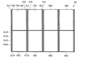
- FIG. 1 is a schematic plan view showing a state of a wafer, which is a semiconductor device according to a first embodiment.
- FIG. 2 is a schematic enlarged plan view of a region surrounded by a round dotted line “II” in FIG. 1.
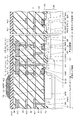
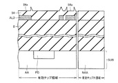
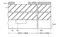
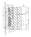
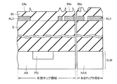
- FIG. 3 is a schematic cross-sectional view showing a configuration of a semiconductor device of an effective chip region and an effective chip outside region according to the first embodiment, corresponding to a region surrounded by a round dotted line “III” in FIG. 1.
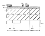
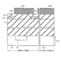
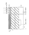
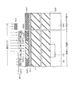
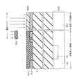
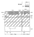
- It is a schematic sectional drawing which shows the 2nd process of the manufacturing method of the semiconductor device in Embodiment 1 of this invention.
- FIG. 6 is a schematic cross-sectional view showing a step corresponding to FIG. 5 of the method for manufacturing the semiconductor device in the first comparative example of the first embodiment of the present invention.
- FIG. 7 is a schematic cross-sectional view showing a step corresponding to FIG. 6 of the method for manufacturing the semiconductor device in the first comparative example of the first embodiment of the present invention.
- FIG. 8 is a schematic cross-sectional view showing a step corresponding to FIG.
- FIG. 9 is a schematic cross-sectional view showing a step corresponding to FIG. 8 of the method for manufacturing the semiconductor device in the first comparative example of the first embodiment of the present invention.
- FIG. 10 is a schematic cross-sectional view showing a step corresponding to FIG. 9 of the method for manufacturing the semiconductor device in the first comparative example of the first embodiment of the present invention.
- FIG. 12 is a schematic cross sectional view showing a step corresponding to FIG. 10 and FIG. 11 of the method for manufacturing the semiconductor device in the first comparative example of the first embodiment of the present invention.
- FIG. 13 is a schematic cross-sectional view showing a step corresponding to FIG.
- FIG. 9 is a schematic cross-sectional view showing a step corresponding to FIG. 8 of the method for manufacturing the semiconductor device in the second comparative example of the first embodiment of the present invention.
- FIG. 10 is a schematic cross-sectional view showing a step corresponding to FIG. 9 of the method for manufacturing the semiconductor device in the second comparative example of the first embodiment of the present invention.
- FIG. 12 is a schematic cross sectional view showing a step corresponding to FIG. 10 and FIG. 11 of the method for manufacturing the semiconductor device in the second comparative example of the first embodiment of the present invention.
- FIG. 13 is a schematic cross-sectional view showing a step corresponding to FIG.
- FIG. 5 is a schematic cross-sectional view showing a step following the step in the method for manufacturing a semiconductor device according to the second embodiment of the present invention.
- FIG. 25 is a schematic cross-sectional view showing a step following the step in the method for manufacturing a semiconductor device according to the second embodiment of the present invention.
- FIG. 26 is a schematic cross-sectional view showing a step following the step of FIG. 25 in the method for manufacturing a semiconductor device in the second embodiment of the present invention. It is a top view of the exposure apparatus used in Embodiment 3 of this invention.
- FIG. 6 is a schematic cross-sectional view showing a process corresponding to FIG. 5 of the method for manufacturing a semiconductor device in the third embodiment of the present invention.
- FIG. 26 is a schematic cross-sectional view showing a step corresponding to FIG. 25 of the method for manufacturing a semiconductor device in the third embodiment of the present invention.
- FIG. 34 is a schematic cross-sectional view showing a step following the step of FIG. 33 in the method for manufacturing a semiconductor device in the fourth embodiment of the present invention.
- FIG. 35 is a schematic cross-sectional view showing a step following the step of FIG.
- FIG. 34 is in the method for manufacturing a semiconductor device in the fourth embodiment of the present invention.
- FIG. 36 is a schematic cross-sectional view showing a step following the step of FIG. 35 in the method for manufacturing a semiconductor device in the fourth embodiment of the present invention.
- FIG. 10 is a schematic plan view illustrating a state of a wafer in a semiconductor device according to a fifth embodiment.
- FIG. 9 is a schematic cross-sectional view showing a step corresponding to FIG. 8 of the method for manufacturing a semiconductor device in the fifth embodiment of the present invention.
- FIG. 40 is a schematic cross-sectional view showing a step following the step of FIG. 39 in the method for manufacturing a semiconductor device in the fifth embodiment of the present invention.
- FIG. 40 is a schematic cross-sectional view showing a step following the step of FIG. 39 in the method for manufacturing a semiconductor device in the fifth embodiment of the present invention.
- FIG. 41 is a schematic cross-sectional view showing a step following the step of FIG. 40 in the method for manufacturing a semiconductor device in the fifth embodiment of the present invention.
- FIG. 42 is a schematic cross-sectional view showing a step following the step of FIG. 41 in the method for manufacturing a semiconductor device in the fifth embodiment of the present invention.
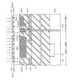
- the semiconductor wafer SW has an effective chip area AA and an effective chip outside area NAA.
- the effective chip area AA is arranged at the center of the semiconductor wafer SW, and a plurality of image sensor chip areas IMC are formed.
- Each of the plurality of chip regions IMC has a rectangular planar shape and is arranged in a matrix.
- an area having the same configuration as that of the chip area IMC (area indicated by a broken line) is formed, but the area is outside the semiconductor wafer SW. It has a planar shape in which a part of the rectangle is cut off by the peripheral edge.
- each of a plurality of chip regions IMC arranged in effective chip region AA includes, for example, a photodiode formation region PDR as a photoelectric conversion element, and a peripheral circuit formation region PCR for controlling the photodiode. And have.
- the formation region PCR is formed on, for example, both sides of the formation region PDR.
- a dicing line region DLR is formed between the plurality of chip regions IMC.
- An alignment mark is arranged in the dicing line region DLR.
- the image sensor controls the photodiode PD (photoelectric conversion element) in the formation region PDR (photodiode portion) of the effective chip region AA and the formation region PCR (peripheral circuit portion). And a transistor CTR.
- this image sensor is formed in the n ⁇ region NTR of the semiconductor substrate SUB made of, for example, silicon.
- the photodiode portion and the peripheral circuit portion are separated from each other in plan view by a field oxide film FO formed on the surface of the semiconductor substrate SUB.
- the effective chip area AA and the effective chip outside area NAA are separated from each other in plan view by a field oxide film FO formed on the surface of the semiconductor substrate SUB.
- the photodiode PD is composed of a p-type well region PWR1 and an n-type impurity region NPR.
- the p-type well region PWR1 is formed on the surface of the semiconductor substrate SUB in the photodiode portion.
- the n-type impurity region NPR is formed on the surface of the semiconductor substrate SUB in the p-type well region PWR1, and forms a pn junction with the p-type well region PWR1.
- a MIS (Metal Insulator Semiconductor) transistor such as a transfer transistor SWTR is also formed.
- the transfer transistor SWTR has a pair of source / drain regions NPR, NNR, NR, a gate insulating film GI, and a gate electrode GE.
- Each of the pair of n-type source / drain regions NPR and NNR, NR are arranged at a distance from each other on the surface of the semiconductor substrate SUB in the p-type well region PWR1.
- One region of the pair of n-type source / drain regions NPR, NNR, and NR is integrated with the n-type impurity region NPR of the photodiode PD and is electrically connected to each other.
- the other region of the pair of source / drain regions NPR, NNR, and NR has an n + impurity region NR as a high concentration region and an n-type impurity region NNR as an LDD (Lightly Doped Drain).
- a gate electrode GE is formed with a gate insulating film GI interposed therebetween.
- a p + impurity region PR is formed on the surface of the semiconductor substrate SUB in the p-type well region PWR1 so as to be connected to the upper wiring.
- An insulating layer is formed on the surface of the semiconductor substrate SUB so as to cover the photodiode PD. One end of this insulating layer rides on one side of the gate electrode GE. A side wall insulating layer is formed on the other side wall of the gate electrode GE as a residue of the insulating layer.
- a p-type well region PWR2 is formed on the surface of the semiconductor substrate SUB in the peripheral circuit portion.
- a control element for controlling the operation of the plurality of photodiodes PD is formed, and this control element includes, for example, a MIS transistor CTR.
- the MIS transistor CTR has a pair of n-type source / drain regions NNR, NR, a gate insulating film GI, and a gate electrode GE.
- Each of the pair of n-type source / drain regions NNR, NR is formed on the surface of the semiconductor substrate SUB at a distance from each other.
- Each of the pair of n-type source / drain regions NNR, NR has, for example, an n-type impurity region NR as a high concentration region and an n-type impurity region NNR as an LDD.
- a gate electrode GE is formed on the surface of the semiconductor substrate SUB sandwiched between the pair of n-type source / drain regions NNR and NR with the gate insulating film GI interposed therebetween.
- a sidewall insulating layer is formed on the sidewall of the gate electrode GE.
- the material of the gate electrode GE of each MIS transistor in the photodiode portion and the peripheral circuit portion may be made of, for example, polycrystalline silicon doped with impurities, or may be made of a metal such as TiN.
- each of the effective chip area AA photodiode part PDR, peripheral circuit part PCR
- the above elements photodiode PD, MIS transistor SWTR, CTR
- An interlayer insulating layer II1 is formed so as to cover it.
- a patterned first-layer metal wiring AL1 is formed on the interlayer insulating layer II1.
- the first-layer metal wiring AL1 is electrically connected to, for example, the p + impurity region PR or the n + impurity region NR through the conductive layer C1 that fills the contact hole of the interlayer insulating layer II1, particularly in the effective chip region AA. ing.
- An interlayer insulating layer II2 is formed on the interlayer insulating layer II1 so as to cover the metal wiring AL1.
- the patterned second-layer metal wiring AL2 is formed on the interlayer insulating layer II2.
- the second-layer metal wiring AL2 is electrically connected to the first-layer metal wiring AL1 through the conductive layer T1 filling the through hole of the interlayer insulating layer II2, particularly in the effective chip area AA.
- the metal wirings AL1 and AL2 in the effective chip area AA and the metal wirings AL1 and AL2 in the effective chip outside area NAA are formed with the same pattern. That is, in the area outside the effective chip NAA, the patterns of the metal wirings AL1 and AL2 similar to those of the photodiode section and the peripheral circuit section of the effective chip area AA are periodically formed. Also in the outside effective chip area NAA, the same control transistor CTR as that in the effective chip area (peripheral circuit section) is formed. However, in the effective chip outside area NAA, the metal wiring AL1 and the metal wiring AL2 may not be electrically connected through the conductive layer T1. In the first place, the metal wirings AL1 and AL2 are formed in the effective chip outside area NAA in FIG. 3, but the metal wirings AL1 and AL2 may not be formed in the effective chip outside area NAA.
- An interlayer insulating layer II3 is formed on the interlayer insulating layer II2 so as to cover the metal wiring AL2.
- a patterned third-layer metal wiring AL3 is formed on the interlayer insulating layer II3.
- This third-layer metal wiring AL3 is electrically connected to the second-layer metal wiring AL2 through a conductive layer T2 filling the through hole of the interlayer insulating layer II3.
- the metal wiring AL3 is formed in the uppermost layer among a plurality of metal wirings to be formed.
- the metal wiring AL3 as the uppermost layer metal wiring is formed in the effective chip area AA, but is not formed in the effective chip outside area NAA. That is, the interlayer insulating layer II3 is formed on the interlayer insulating layer II2 also in the effective chip outside region NAA, but the metal wiring AL3 is not formed on the interlayer insulating layer II3 in the effective chip outside region NAA.
- An interlayer insulating layer II4 is formed on the interlayer insulating layer II3 so as to cover the metal wiring AL3 in the effective chip region.
- the interlayer insulating layer II4 is formed in both the effective chip area AA and the effective chip outside area NAA.
- a passivation film PASF is formed on the interlayer insulating layer II4.
- a condensing lens LS is disposed on the passivation film PASF and just above the photodiode PD. The condensing lens LS is for collecting light and irradiating the photodiode PD.
- the metal wirings AL1 to AL3 are preferably made of a metal material such as aluminum, but may be made of a metal material such as copper instead of aluminum.
- Interlayer insulating layers II1, II2, II3, and II4 are made of, for example, silicon oxide films, and have an etching selectivity (for example, an interlayer insulating layer for forming conductive layers T1, T2, etc.) with metal wirings AL1 to AL3 made of a metal material.
- II2 and II3 are made of materials having different etching selectivity ratios.
- the conductive layers C1, T1, T2 preferably have a configuration in which through holes formed in the interlayer insulating layer are filled with a metal material such as tungsten.
- a barrier metal may be formed on the side wall or bottom wall of the through hole forming the conductive layers C1, T1, T2.
- FIG. 3 also shows the photodiode PD and switching element SWTR in the photodiode section, the control transistor CTR in the peripheral circuit section, etc. one by one. However, actually, for example, a plurality of photodiodes PD, switching elements SWTR, and the like are arranged at intervals from each other in each of the divided chip regions IMC shown in FIGS.
- FIG. 3 a method for manufacturing the semiconductor device of the present embodiment shown in FIG. 3 will be described with reference to FIGS.
- detailed description of the method of forming the interlayer insulating layer II3 and the layers below the interlayer insulating layer II3 shown in FIG. 3 will be omitted, so that the layers shown in FIGS. In comparison, the illustration is simplified.
- the photodiode portion and the peripheral circuit portion are collectively referred to as an effective chip region.
- the photodiode PD and interlayer insulating layers II1 to II3 shown in FIG. 3 are formed on the surface of the semiconductor substrate SUB made of a different semiconductor material depending on the wavelength of light irradiated during use, such as silicon and germanium.
- these are collectively shown as an interlayer insulating layer II
- metal wirings AL1, AL2, conductive layers T1, T2, etc. are formed, and then interlayer insulation is performed in both the effective chip region and the effective chip outside region.
- Metal film AL3 is formed so as to cover the upper surface of layer II3.
- the metal film AL3 is an uppermost metal layer that becomes the uppermost metal wiring AL3 of FIG. 3 by patterning described later, and is formed by sputtering, for example.
- the metal wiring AL3 which is the uppermost metal wiring is preferably formed to be thicker than the metal wirings AL1 and AL2, for example, 600 nm or more.
- the metal layer photoresists RSP1 and RSP2 are formed on the uppermost metal layer AL3 in both the effective chip region and the region outside the effective chip.
- the photoresist formed here is a so-called positive photoresist in which a region irradiated with light during exposure is dissolved by development.
- the photomask MK1a is a patterning product mask in which a light shielding pattern PTa made of, for example, chromium is formed on the surface of a base body BS1a made of, for example, glass.
- a light shielding pattern PTa made of, for example, chromium is formed on the surface of a base body BS1a made of, for example, glass.
- the positive photoresist in the region that is not irradiated with light by the pattern PTa of the photomask MK1a is exposed to the positive photoresist in the region that is irradiated by RSP1 without being affected by the pattern PTa of the photomask MK1a.
- RSP2 the area outside the effective chip is preferably not exposed.
- the photomask MK2a is a special mask made of, for example, only a glass base body BS2a and having no light shielding pattern made of chromium or the like. For this reason, the entire photoresist outside the effective chip is irradiated with light to become a positive photoresist RSP2. At this time, the effective chip area is preferably not exposed.
- the photoresist in the effective chip area is exposed, the photoresist in the area outside the effective chip is exposed. However, after the photoresist in the area outside the effective chip is exposed, the photoresist in the effective chip area may be exposed.
- the positive photoresist in the effective chip region and in the effective chip outside region is exposed, a portion in the effective chip region and a portion in the effective chip outside region of the positive photoresist are exposed. It is developed at the same time.
- the positive photoresist RSP2 is dissolved in the effective chip region and the region outside the effective chip, and the positive photoresist RSP1 remains. That is, all the positive photoresist in the area outside the effective chip is removed, and the pattern of the positive photoresist RSP1 is formed.
- uppermost metal layer AL3 is patterned using patterned positive photoresist RSP1 as a mask.
- the uppermost metal layer AL3 in the effective chip area is patterned, the uppermost metal wiring AL3 is formed, and the uppermost metal layer AL3 in the entire area outside the effective chip is removed. Thereafter, the photoresist RSP1 is removed.
- interlayer insulating layer II4 is formed on both the effective chip region and the effective chip outside region so as to cover interlayer insulating layer II3 and uppermost layer metal wiring AL3.
- the interlayer insulating layer II4 is made of, for example, a silicon oxide film, and is formed by using, for example, a CVD (Chemical Vapor Deposition) method.
- the uppermost surface of the interlayer insulating layer II4 is formed so as to rise upward in the region on the metal wiring AL3 as compared with the other regions.
- Interlayer insulating layer II4 preferably has a thickness of 600 nm or more, for example.
- a positive photoresist is formed on the interlayer insulating layer II4 in both the effective chip region and the region outside the effective chip.
- the positive photoresists RSP1 and RSP2 are removed by selectively etching a part of the upper surface before performing the step of planarizing the upper surface of the interlayer insulating layer II4. It is a photoresist to be formed.
- the photomask MK1b is a product mask for patterning in which a light shielding pattern PTb made of, for example, chromium is formed on the surface of a base body BS1b made of, for example, glass.
- the pattern PTb of the photomask MK1b is preferably formed in a region that does not overlap with the metal wiring AL3 in the effective chip region in plan view. In other words, it is preferable that the positive photoresist in a region that overlaps with the metal wiring AL3 in a plan view (a region located directly above the metal wiring AL3) is exposed to light and becomes the photoresist RSP2.
- the positive type photoresist outside the effective chip is not exposed.
- the entire positive type photoresist outside the effective chip is RSP1.
- the positive photoresist is developed both in the effective chip region and in the effective chip outside region, the positive photoresist RSP2 is dissolved, and the positive photoresist RSP1 remains. At this time, the positive photoresist RSP1 remains in the entire area outside the effective chip.
- interlayer insulating layer II4 is patterned in the effective chip region using the pattern of patterned positive photoresist RSP1 (pre-etching photoresist) as a mask. Then, a part of the upper surface of the interlayer insulating layer II4 is selectively etched in a region where the positive photoresist RSP1 does not remain, and the upper surface is formed in a deeper II4a. This process is called so-called pre-etching.
- the upper surface of the interlayer insulating layer II4 is etched by the pre-etching in the interlayer insulating layer II4 in a region located immediately above the metal wiring AL3 patterned in the effective chip region. This is because, as described above, the photoresist RSP2 is designed to be exposed almost right above the region where the metal wiring AL3 is patterned in the effective chip region.
- the upper surface of the interlayer insulating layer II4 is formed so as to rise above the other regions in the region located directly above the metal wiring AL3. Therefore, a part of the upper surface of the interlayer insulating layer II4 located directly above the metal wiring AL3 is selectively pre-etched, so that a step on the upper surface of the interlayer insulating layer II4 can be reduced. Therefore, the upper surface of the interlayer insulating layer II4 can be processed more flatly in the subsequent process. However, a region that is not selectively pre-etched may be included in a part of the upper surface of the interlayer insulating layer II4 located immediately above the metal wiring AL3.
- the entire interlayer insulating layer II4 is covered with the photoresist RSP1. For this reason, the interlayer insulating layer II4 is not pre-etched. Referring to FIG. 11, photoresist RSP1 is thereafter removed.
- interlayer insulating layer II4 is polished and planarized by, for example, CMP (Chemical Mechanical Polishing) by pre-etching in FIG. 10 in the entire effective chip region and the region outside effective chip. Thereafter, the passivation film PASF and the lens LS (see FIG. 3) are formed, whereby the semiconductor wafer SW (semiconductor device) having the image sensor shown in FIG. 3 is formed. Detailed description of the method of forming the passivation film PASF and the lens LS is omitted.
- CMP Chemical Mechanical Polishing
- FIGS. 13 to 23 are comparative examples of the present embodiment.
- the photomask MK2a is a patterning product in which a light shielding pattern PTa made of, for example, chromium is formed on the surface of a base body BS2a made of, for example, glass, like the photomask MK1a. It is a mask.
- the process of FIG. 13 may be performed before the process of FIG. 4 or may be performed simultaneously with the process of FIG.
- the positive photoresists RSP1 and RSP2 in the effective chip area and the effective chip outside area are simultaneously developed in the same manner as in the step of FIG. Then, the pattern of the positive photoresist RSP1 is formed both in the effective chip region and in the effective chip outside region.
- the uppermost metal layer AL3 is patterned using the pattern of the positive photoresist RSP1 of FIG. 14 as a mask, and then the photoresist RSP1 is removed.
- the pattern of the metal wiring AL3 remains in the vicinity of the outer edge of the semiconductor wafer (the outermost edge of the semiconductor substrate SUB in plan view), for example, a member for fixing the semiconductor wafer is attached to the portion. There is a possibility that the metal wiring AL3 is scraped and foreign matter is generated. For this reason, the photoresist in a region within a certain distance (for example, 1.5 mm or more) from the outer edge of the semiconductor wafer is removed.
- interlayer insulating layer II4 is formed in the same manner as in the process of FIG. In both the effective chip region and the region outside the effective chip, a positive photoresist for pre-etching the upper surface of the interlayer insulating layer II4 is formed on the interlayer insulating layer II4.
- the photomask MK2b is a product mask for patterning in which a light shielding pattern PTb made of, for example, chromium is formed on the surface of a base body BS2b made of, for example, glass.
- the order of exposure of the effective chip area and the area outside the effective chip is arbitrary.
- positive photoresists RSP1 and RSP2 in the effective chip area and in the outside area of the effective chip are developed in the same manner as in the process of FIG.
- FIG. 18 in the region where photoresist RSP2 is dissolved, a part of interlayer insulating layer II4 is patterned (pre-etched) in the same manner as in the step of FIG. 10, and the upper surface thereof is deepened to II4a.
- the photoresist RSP1 is removed as in the step of FIG. 11, referring to FIG. 19, the upper surface of interlayer insulating layer II4 is planarized by CMP as in the step of FIG.
- a region having a certain thickness from the uppermost surface is preliminarily etched (preetched).
- the upper surface is flattened by CMP.
- the interlayer insulating layer II4 is pre-etched also in the area outside the effective chip. For this reason, as shown in FIG. 18, the upper surface II4a of the interlayer insulating layer II4 reaches deeper than other regions in the vicinity of the outermost edge of the semiconductor wafer.
- CMP shown in FIG. 19 is performed in this state, the upper surface of the interlayer insulating layer II4 is polished deeper in the vicinity of the outer edge, and the uppermost surface reaches II4b. Then, the metal wiring AL3 under the interlayer insulating layer II4 is polished so as to be exposed on the uppermost surface at the outermost portion, and there is a possibility that foreign matter of the metal wiring AL3 is generated.
- the uppermost surface of the effective chip outside region is pre-etched by stopping the pre-etching in the effective chip outside region as in the second comparative example of the present embodiment shown below. It is preferable to suppress deeper polishing. In this way, it is possible to prevent the upper portion of the interlayer insulating layer II4 from being excessively polished at the outermost part of the area outside the effective chip during CMP.
- the pattern of metal wiring AL3 is formed in both the effective chip region and the region outside the effective chip. .
- an interlayer insulating layer II4 is formed as in the step of FIG. After the positive photoresist is formed, only the effective chip area is exposed by the photomask MK1b. The positive type photoresist outside the effective chip is not exposed.
- the positive photoresists RSP1 and RSP2 in the effective chip area and the effective chip outside area are developed in the same manner as in the step of FIG.
- the photoresist RSP1 remains in the entire area outside the effective chip.
- the upper surface of interlayer insulating layer II4 is flattened by CMP as in the step of FIG.
- a step LDF occurs on the upper surface of the interlayer insulating layer II4 in the vicinity of the boundary between the effective chip region and the region outside the effective chip. This is because, in the region outside the effective chip, the interlayer insulating layer II4 is not pre-etched in FIG. 22 at all, so that the thickness (region) in which the interlayer insulating layer II4 is to be etched by CMP is increased in the region outside the effective chip. is there. Since the amount of the interlayer insulating layer II4 to be removed is larger in the area outside the effective chip than in the effective chip area, as shown in FIG.
- the uppermost surface of the interlayer insulating layer II4 in the area outside the effective chip is A level difference LDF is generated so as to be higher than the top surface. For this reason, image unevenness may occur in the image sensor in the effective chip region, particularly in the vicinity of the boundary between the effective chip region and the region outside the effective chip.
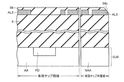
- the uppermost layer metal wiring AL3 is formed only in the effective chip region, the uppermost interlayer insulating layer II4 is formed, and only the interlayer insulating layer II4 in the effective chip region is pre-etched.
- the uppermost layer metal wiring AL3 is not arranged at all in the area outside the effective chip, for example, as shown in FIG.
- the uppermost surface is formed at a low position.
- the difference in (thickness) is small (compared to the case of FIG. 22 for example). Therefore, the step between the effective chip region and the effective chip outside region can be reduced by performing the CMP process on the interlayer insulating layer II4 between the effective chip region and the effective chip outside region in the process of FIG.
- the metal wiring AL3 is not formed at all in the region outside the effective chip, the uppermost surface of the interlayer insulating layer II4 in the region outside the effective chip is substantially flat (even if pre-etching is not performed), and the height in the vertical direction is This is almost the same as the uppermost surface II4a of the effective chip region after the pre-etching. For this reason, by selectively pre-etching only the interlayer insulating layer II4 in the effective chip region, in the subsequent CMP process, it is possible to process more flatly without causing a step between the effective chip region and the region outside the effective chip. it can.
- the metal wiring AL3 is not formed at all in the area outside the effective chip, the generation of foreign matters due to the metal wiring AL3 in the vicinity of the outer edge of the area outside the effective chip is suppressed in a subsequent process such as CMP.
- the present embodiment it is possible to planarize the uppermost surface of the uppermost interlayer insulating layer without generating foreign matters due to the metal wiring AL3 in the vicinity of the outer edge of the effective chip outer region. As a result, it is possible to suppress deterioration of the optical characteristics of the outermost image sensor in the effective chip area.
- Embodiment 2 The present embodiment is different from the first embodiment in the procedure for patterning the uppermost metal wiring AL3.
- a method for manufacturing the semiconductor device of the present embodiment will be described with reference to FIGS.
- only differences from the manufacturing method of the first embodiment will be described.
- the positive photoresist on metal wiring AL3 in the effective chip region is exposed through photomask MK1a which is a product mask. Thereafter, development is performed immediately, and the metal wiring AL3 in the effective chip region is patterned. At this time, the area outside the effective chip is preferably not exposed.
- the entire positive photoresist on the metal wiring AL3 in the area outside the effective chip is exposed through the photomask MK2a which is a special mask. At this time, the effective chip area is preferably not exposed.
- the positive photoresist in the area outside the effective chip is dissolved by development. Thereafter, the uppermost metal layer AL3 in the entire area outside the effective chip is removed in the same manner as in FIG. 7, and thereafter the same processes as in FIGS. 8 to 12 are performed in the same manner as in the first embodiment. That is, in this embodiment, the step of developing the portion of the positive photoresist in the effective chip region and the step of developing the portion of the positive photoresist in the region outside the effective chip are performed in separate steps.
- the effective chip area is exposed and developed, the area outside the effective chip is exposed and developed.
- the effective chip area may be exposed and developed after the area outside the effective chip is exposed and developed.
- the positive photoresist formed on the uppermost metal layer AL3 is exposed in either the effective chip region or the effective chip outside region. Then, before developing this, exposure is performed in either the effective chip area or the effective chip outside area. Thereafter, the positive type photoresist in both the effective chip area and the effective chip outside area is simultaneously developed.
- the positive photoresist is exposed and developed in either the effective chip region or the effective chip outside region, and after the lower wiring layer AL3 is patterned, the effective chip is formed. Exposure and development are performed in either the region or the region outside the effective chip. That is, in the second embodiment, the time from exposure to development and patterning is shorter than that in the first embodiment.
- the effective chip area and the effective chip outside area are exposed first, and then the effective chip area and the effective chip outside area are collectively developed.
- the work efficiency is higher than that of the second embodiment.
- the time from the exposure of the effective chip region to the patterning of the metal layer AL3 in the effective chip region is long as in the first embodiment, the region in which the metal layer AL3 is removed by the patterning in plan view may vary. There is. Therefore, by reducing the time from exposure to patterning of the metal layer AL3 in each region as in the present embodiment, for example, variation in shape and size in the region where the metal layer AL3 is removed by patterning in a plan view is suppressed. can do.
- the second embodiment of the present invention is different from the first embodiment of the present invention only in each of the points described above. That is, the configuration, conditions, procedures, effects, and the like that have not been described above for the second embodiment of the present invention are all in accordance with the first embodiment of the present invention.
- the present embodiment is different from the first embodiment in the method of adjusting the area where the positive photoresist in the area outside the effective chip is exposed.
- the region where the positive photoresist is exposed is adjusted, for example, by the blind function of a stepper (reduced projection exposure apparatus) built in the exposure apparatus.
- a stepper reduced projection exposure apparatus
- FIGS. 27 and 28 in the non-exposure region NEP that overlaps with a light shielding plate called a blind BLD in plan view, light from the light source is blocked by the blind BLD even in the exposure area. However, it does not reach the photomask MK or the semiconductor wafer SW.
- the light from the light source reaches the photomask MK, and if it does not overlap with the pattern PT in plan view, the light reaches the semiconductor wafer SW.
- the photomask MK composed of the glass base body BS and the pattern PT such as chrome is for explaining the photomask MK1a and the photomask MK2a together.
- the exposure area to which light is supplied may be prepared such that light is supplied to the entire photomask MK1a in the effective chip area and no light is supplied to the area outside the effective chip by blind BLD.
- the entire positive photoresist in the area outside the effective chip is exposed.
- the entire area outside the effective chip is exposed by the blind BLD without using the photomask MK2a, and a portion other than the area outside the effective chip (for example, the effective chip area) is adjusted to be shielded from light.
- the same steps as in FIGS. 6 to 12 are performed as in the first embodiment.
- the photoresist in the entire area outside the effective chip is exposed by the blind BLD. Adjustment is performed and exposure processing is performed. Thereafter, the same steps as in FIG. 26 and FIGS. 8 to 12 are performed as in the second embodiment.
- the passivation film PASF, the lens LS, and the like a semiconductor device having the same aspect as that of the first embodiment shown in FIG. 3 is formed.
- a region exposed on the semiconductor wafer SW is controlled exclusively by a photomask.
- a region exposed on the semiconductor wafer SW is controlled by using a photomask and a blind BLD together. Particularly in the area outside the effective chip, the entire positive photoresist on the metal wiring AL3 is exposed. Therefore, by using the blind BLD, it is possible to control the exposure region so that the entire photoresist outside the effective chip region is exposed and the photoresist in the effective chip region is not exposed without using the photomask MK2a. Therefore, the manufacturing cost of the semiconductor wafer SW is reduced by the amount that the photomask MK2a for patterning (removing) the uppermost metal layer AL3 in the area outside the effective chip is unnecessary.
- the third embodiment of the present invention is different from the first embodiment of the present invention only in each point described above. That is, the configuration, conditions, procedures, effects, and the like that have not been described above for the third embodiment of the present invention are all in accordance with the first embodiment of the present invention.
- the present embodiment differs from the first embodiment in the configuration of the uppermost metal wiring, the photoresist used, and the patterning method.
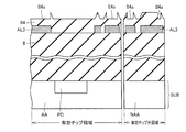
- the structure of the semiconductor device of this embodiment will be described with reference to FIG. Only differences from the semiconductor device of the first embodiment will be described here.
- the image sensor as the semiconductor device of the present embodiment has roughly the same configuration as the semiconductor device of the first embodiment shown in FIG.
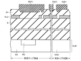
- FIG. 32 is different from FIG. 3 in that the metal wiring AL3 of the uppermost layer is arranged in the area outside the effective chip NAA as well as the effective chip area AA.
- the uppermost metal wiring AL3 and the lower metal wiring AL2 and metal wiring AL1 are not electrically connected through the conductive layer T1, but these are electrically connected through the conductive layers T1 and T2. May be.
- the uppermost metal layer is patterned in both the effective chip region and the effective chip outer region to form uppermost metal wiring AL3. Therefore, although not shown, in this embodiment, the photomask MK2a (see FIG. 5) for patterning the uppermost metal layer AL3 in the region outside the effective chip is the photomask MK1a for patterning the uppermost metal layer AL3 in the effective chip region. Similar to (see FIG. 4), the mask is a product mask in which, for example, a light-shielding pattern made of chromium is formed on the surface of a base body BS1a made of glass.
- the photomask MK1a in the effective chip area and the photomask MK2a in the area outside the effective chip are integrated and formed on the uppermost metal layer AL3 in the effective chip area and the uppermost metal layer AL3 in the effective chip area.
- a positive photoresist for patterning the uppermost metal layer AL3 may be exposed and developed simultaneously. Further, the uppermost metal layer AL3 in the effective chip region and the uppermost metal layer AL3 in the region outside the effective chip may be patterned at the same time.
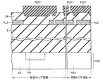
- an interlayer insulating layer II4 is formed in the same manner as in the step of FIG. 8, and a negative photo for pre-etching the upper surface of the interlayer insulating layer II4 on the interlayer insulating layer II4 in both the effective chip region and the effective chip outside region.
- a resist is formed.
- the photomask MK1c is a patterning product mask in which, for example, a light shielding pattern PTc made of chromium, for example, is formed on the surface of a glass base body BS1c.
- the pattern PTc of the photomask MK1c is preferably formed in a region that overlaps the metal wiring AL3 in the effective chip region in a plan view (a region located directly above the metal wiring AL3).
- the negative photoresist in a region that does not overlap with the metal wiring AL3 in plan view is designed to be exposed to the photoresist RSN2.
- the photomask MK2c is a product mask for patterning in which a light-shielding pattern PTc made of, for example, chrome is formed on the surface of a base body BS2c made of, for example, glass.
- a light-shielding pattern PTc made of, for example, chrome is formed on the surface of a base body BS2c made of, for example, glass.
- the order of exposure of the effective chip area and the area outside the effective chip is arbitrary.
- the photoresist on the interlayer insulating layer II4 is a negative type photoresist, contrary to the positive type photoresist, in the region where light is irradiated, the negative photoresist RSN1 is formed, and in the region where light is not irradiated. This is a negative photoresist RSN2.
- the negative photoresist on the outer edge of the area outside the effective chip is exposed (peripheral exposure). Similar to the third embodiment, this peripheral exposure may be performed by shielding the area other than the outer edge of the effective chip outer area with a blind BLD of a stepper (reduction projection type exposure apparatus) built in the exposure apparatus.
- the region other than the outer edge portion of the effective chip outer region means a region farther inward from the outer edge of the semiconductor substrate SUB than the outer edge portion of the effective chip outer region in plan view.
- the outer edge side of the effective chip outer region is an exposure area, and the other than the outer edge portion of the effective chip outer region in the exposure area is shielded, and only the outer edge portion closest to the outer edge in the effective chip outer region. Are exposed.
- the position farthest from the outer edge which is the outermost portion of the semiconductor substrate SUB is the uppermost metal wiring AL3 in the effective chip outer region, and It is preferable that the distance from the outer edge is 0.5 mm or more from the uppermost metal wiring AL3 located closest to the outer edge.
- the peripherally exposed region (outer edge portion) is arranged on the outermost side in the effective chip outer region from the outer edge of the semiconductor substrate SUB (the outermost edge of the uppermost metal wiring AL3 closest to the outer edge of the semiconductor substrate SUB).
- the semiconductor substrate SUB It is preferable to occupy a region up to a distance of 0.5 mm or more inside the semiconductor substrate SUB in a plan view from the position EA.
- the distance from the outer edge of the semiconductor substrate SUB to the outermost position EA of the uppermost metal wiring AL3 in the effective chip outer region is preferably 1.5 mm or more. Therefore, it is preferable that the peripheral exposure is performed in a region closer to the outer edge of the semiconductor substrate SUB than a position where the distance from the outer edge of the semiconductor substrate SUB is 2.0 mm or more.
- the semiconductor wafer when exposing only the outer edge portion of the area outside the effective chip using the blind BLD of the exposure apparatus as shown in FIG. 34, for example, the semiconductor wafer is placed on a turntable having a circle in plan view. It is preferable that SW is mounted.
- the turntable rotates in the direction of the arrow in FIG. 35 about the lower rotation axis.
- negative photoresists RSN1 and RSN2 are formed as shown in FIGS. 33 and 34, for example.
- the negative photoresists RSN1 and RSN2 on the semiconductor wafer SW are collectively shown as negative photoresists RS1 and RS2.
- the outer edge (peripheral exposure region) of the semiconductor wafer SW is exposed by the light source and the blind BLD of the exposure apparatus installed so as to be fixed immediately above the outer edge of the semiconductor wafer SW. Only) is exposed.
- the photoresist exposed by the light source is denoted as RS1
- the photoresist not exposed is denoted as RS2.
- the negative photoresist is developed both in the effective chip region and in the effective chip outside region, the negative photoresist RSN2 is dissolved, and the negative photo resist is dissolved. Resist RSN1 remains.
- the upper surface of interlayer insulating layer II4 is selectively patterned in both the effective chip region and the effective chip outside region. Is done. Then, a part of the upper surface of the interlayer insulating layer II4 is selectively etched (pre-etched) in a region where the negative photoresist RSN1 does not remain, and the upper surface is formed in a deeper II4a.
- the upper surface of the interlayer insulating layer II4 is etched by the pre-etching in the region located immediately above the patterned metal wiring AL3 in both the effective chip region and the region outside the effective chip. preferable. This is because, as described above, the photoresist RSN2 is designed not to be exposed almost directly above the region where the metal wiring AL3 is patterned in the effective chip region. However, a region that is not selectively pre-etched may be included in a part of the upper surface of the interlayer insulating layer II4 located immediately above the metal wiring AL3.
- the removal of the photoresist RSN1 and the same process as in FIG. 12 are performed.
- the passivation film PASF and the lens LS see FIG. 32
- the semiconductor wafer SW semiconductor device having the image sensor shown in FIG. 32 is formed.
- the pattern of the uppermost metal wiring AL3 is formed in both the effective chip area and the effective chip outside area.
- the interlayer insulating layer II4 covering the uppermost metal wiring AL3 is etched by the negative photoresists RSN1 and RSN2.
- the negative photoresist has the property of remaining in the exposed area. Therefore, if the outer edge portion of the semiconductor substrate SUB on which the negative photoresist is formed is exposed, regardless of the pattern of the photomask MK2c for patterning the interlayer insulating layer II4, the outer edge portion on the interlayer insulating layer II4 The photoresist is exposed and remains as a photoresist pattern after etching. Therefore, the interlayer insulating layer II4 at the outer edge is protected by the pattern of the negative photoresist RSN1, and even if the interlayer insulating layer II4 in the area outside the effective chip is pre-etched, the vicinity of the outermost EA of the uppermost metal wiring AL3 is etched. Is suppressed.
- the outermost area outside the effective chip is exposed using a negative photoresist for patterning the interlayer insulating layer, so that the uppermost metal wiring is formed in the area outside the chip and the uppermost layer is formed. Even if the interlayer insulating layer is pre-etched, etching of the uppermost metal wiring can be suppressed. Therefore, according to the present embodiment, the pre-etching of the interlayer insulating layer suppresses the generation of a step on the uppermost surface of the interlayer insulating layer after the CMP process, while suppressing the generation of foreign matter due to the metal wiring, The uppermost surface of the uppermost interlayer insulating layer can be planarized.
- exposure is performed at the peripheral exposure by shielding the area other than the outer edge of the effective chip outer area by using the stepper blind BLD at the peripheral exposure.
- the power region can be controlled with high accuracy. Since the area to be peripherally exposed is provided 0.5 mm or more from the outermost EA of the uppermost metal wiring AL3 to the inside of the semiconductor substrate SUB, an interlayer insulating layer II4 for protecting the uppermost metal wiring AL3 is provided on the semiconductor substrate. It can be formed so as to extend from the outer edge of the SUB to a sufficiently inner region.
- the production cost of the special mask can be suppressed. Furthermore, by patterning the uppermost metal layer AL3 without using a special mask, the dimensional accuracy of the uppermost metal layer AL3 is improved.
- the fourth embodiment of the present invention is different from the first embodiment of the present invention only in each point described above. That is, in the fourth embodiment of the present invention, all the configurations, conditions, procedures, effects, and the like not described above are in accordance with the first embodiment of the present invention.
- the present embodiment is different from the first embodiment in the configuration of the uppermost metal wiring and the patterning method. First, the configuration of a semiconductor device in a wafer state as this embodiment will be described.
- semiconductor wafer SW of the present embodiment has roughly the same configuration as semiconductor wafer SW of Embodiment 1 shown in FIG.
- the special exposure area LL is formed in the vicinity of the boundary between the effective chip area AA and the effective chip outside area NAA.
- the special exposure area LL is an area adjacent to the effective chip area in the effective chip outside area, and is an area closest to the effective chip area in the effective chip outside area.
- the special exposure region LL is a region that is selectively exposed in the region outside the effective chip when the uppermost interlayer insulating layer II4 is patterned.
- the image sensor formed in the present embodiment has a configuration in which the pattern of the uppermost metal wiring AL3 is arranged also in the region outside the effective chip.
- the uppermost metal layer is patterned in both the effective chip region and the effective chip outside region, and the uppermost metal wiring is formed.
- AL3 is formed.
- an interlayer insulating layer II4 is formed in the same manner as in the process of FIG. 8, and a positive photo for pre-etching the upper surface of the interlayer insulating layer II4 on the interlayer insulating layer II4 in both the effective chip region and the effective chip outside region.
- a resist is formed.
- the positive photoresist in the effective chip region is selectively exposed.
- the photomask MK2b the positive photoresist in the area outside the effective chip is selectively exposed.
- the order of exposure of the effective chip area and the area outside the effective chip is arbitrary.
- the effective chip is used by the blind BLD of the stepper (reduction projection type exposure apparatus) built in the exposure apparatus, as in the third embodiment.
- the area where the positive photoresist is exposed in the outer area is specified.
- the blind BLD is adjusted so that only an area within a distance of 1 mm or less from the boundary with the effective chip area among the areas outside the effective chip is selectively exposed.
- the positive photoresist is developed both in the effective chip region and in the effective chip outside region, the positive photoresist RSP2 is dissolved, and the positive photo resist is dissolved. Resist RSP1 remains.
- the positive photoresist RSP2 is dissolved only in a part of the region located adjacent to the effective chip region (the distance from the effective chip region is within 1 mm) in the region outside the effective chip.
- the positive photoresist RSP1 remains in other regions.
- interlayer insulating layer II4 is patterned both in the effective chip region and in the region outside the effective chip, using the pattern of patterned positive photoresist RSP1 (pre-etching photoresist) as a mask.
- RSP1 pre-etching photoresist
- the interlayer insulating layer II4 in the region located immediately above the metal wiring AL3 patterned in the effective chip region is etched.
- a part of the upper surface of the interlayer insulating layer II4 located immediately above the metal wiring AL3 located adjacent to the effective chip area is selectively etched.
- a part of the upper surface of the interlayer insulating layer II4 is pre-etched only in a region located adjacent to the effective chip region.
- the top surface of the pre-etched interlayer insulating layer II4 becomes II4a. Thereafter, the photoresist RSP1 is removed.
- interlayer insulating layer II4 is flattened by CMP, for example, in the entire effective chip region and effective chip outside region.
- the pattern of the uppermost metal wiring AL3 is formed in both the effective chip area and the effective chip outside area.
- the positive photoresist RSP2 positioned immediately above the metal wiring AL3 positioned adjacent to the effective chip area is exposed, and the positive photoresist RSP1 in other areas is not exposed.
- the interlayer insulating layer II4 in the region outside the effective chip is etched only in the region immediately above the metal wiring AL3 located adjacent to the effective chip region, and the interlayer insulating layer II4 in the other region outside the effective chip region is etched. It remains without.
- the interlayer insulating layer II4 in the region outside the effective chip is pre-etched, the interlayer insulating layer II4 in the vicinity of the outer edge of the region outside the effective chip is protected by the positive photoresist RSP1 thereon. . Therefore, when a part of the interlayer insulating layer II4 in the region outside the effective chip is pre-etched, a part of the metal wiring AL3 therebelow is etched and a problem that foreign matter is generated can be suppressed.
- the upper surface of the interlayer insulating layer II4 is pre-etched in a region near the effective chip region even in the region outside the effective chip. Therefore, in the CMP shown in FIG. 42, the thickness (area) in which the interlayer insulating layer II4 is to be removed in the area close to the effective chip area in the area outside the effective chip is, for example, the second embodiment of the present embodiment shown in FIG. As in the comparative example, the interlayer insulating layer II4 is reduced in the region outside the effective chip as compared with the case where the pre-etching is not performed at all.
- the upper surface of the insulating layer II4 is not pre-etched at all.
- the position where the step LDF is formed is compared to the case where the interlayer insulating layer II4 is not pre-etched at all in the region outside the effective chip as shown in FIG. It moves to the side near the outer edge of the semiconductor substrate SUB.
- the flatness after the upper surface of the interlayer insulating layer II4 is planarized can be increased at least in the entire effective chip region, and the optical characteristics of the photodiode PD can be improved. it can. Even if the step LDF is formed in the area outside the effective chip, since the photodiode PD does not exist, the step LDF in the area outside the effective chip does not significantly affect the optical characteristics of the image sensor.
- the etching of the uppermost metal wiring is suppressed by the protection of the interlayer insulating layer II4 in the vicinity of the outer edge of the semiconductor substrate SUB, and the interlayer insulating layer II4 close to the effective chip region also in the effective chip outer region. Is pre-etched, the flatness of the uppermost surface of the interlayer insulating layer at least in the effective chip region can be increased.
- the production cost of the special mask can be suppressed. Furthermore, by patterning the uppermost metal layer AL3 without using a special mask, the dimensional accuracy of the uppermost metal layer AL3 is improved.
- the fifth embodiment of the present invention is different from the first embodiment of the present invention only in each of the points described above. That is, the configuration, conditions, procedures, effects, and the like that have not been described above for the fifth embodiment of the present invention are all in accordance with the first embodiment of the present invention.
- the present invention can be applied particularly advantageously to a semiconductor device having an optical conversion element and a manufacturing method thereof.
- AA effective chip area AL1 metal wiring, BS, BS1a, BS2a, BS1b, BS2b, BS1c, BS2c base body, C1, T1, T2 conductive layer, CTR control transistor, DLR dicing line area, EA top layer metal wiring outermost EXP exposure region, FO field oxide film, GE gate electrode, GI gate insulating film, II1, II2, II3, II4 interlayer insulating layer, IMC chip region, LDF step, LL special exposure region, MK1a, MK2a, MK1b, MK2b, MK1c, MK2c Photomask, NAA effective chip area, NEP non-exposed area, NNR, NR n-type area, NPR n-type impurity area, NTR n ⁇ area, PASF passivation film, PCR, PDR formation area, PD photodiode, PR p-type region, PT, PTa PTb, PTc pattern, PWR
Landscapes
- Solid State Image Pick-Up Elements (AREA)
Abstract
工程を煩雑にすることなく最上面が平坦化され、かつ色ムラを抑制するなど光学特性を向上することが可能な光学変換素子(PD)を有する半導体装置の製造方法は、半導体基板(SUB)の主表面の、光電変換素子(PD)が形成された有効チップ領域(AA)と、有効チップ外領域(NAA)との双方において最上層金属層(AL3)が形成される。有効チップ領域(AA)内の最上層金属層(AL3)がパターニングされ、かつ有効チップ外領域(NAA)全体の最上層金属層(AL3)が除去される。有効チップ領域(AA)においてパターニングされた最上層金属層(AL3)を覆うように有効チップ領域(AA)と有効チップ外領域(NAA)との双方に層間絶縁層(II4)が形成される。有効チップ領域(AA)内においてパターニングされた最上層金属層(AL3)の真上に位置する層間絶縁層(II4)の上面の一部が選択的にエッチングされることにより除去された上で、層間絶縁層(II4)の上面が平坦化される。
Description
本発明は、半導体装置およびその製造方法に関し、特に、フォトダイオードなどの光電変換素子を含む半導体装置およびその製造方法に関するものである。
デジタルカメラの特にデジタル一眼レフに使われるイメージセンサは、たとえばシリコンなどの半導体基板からなるチップの主表面上に形成される。イメージセンサを構成する半導体基板とマイクロレンズとの距離が、チップの主表面上の位置(チップの主表面の中央部または外縁の近傍)に応じて変化することがある。この変化により、半導体基板の主表面の中央部のうち、イメージセンサを構成するフォトダイオードなどの光学変換素子が多数配置されるセンサエリア(フォトダイオード部)と、センサエリアの外側であり周辺回路が配置される領域(周辺回路部)との間で、回路を構成する積層構造の最上面に段差が生じる。この段差は、フォトダイオード部と周辺回路部との間で、積層構造の最上層として形成される金属配線の、平面視における占有率が異なることに起因する。
具体的には、上記フォトダイオード部よりも周辺回路部の方が、一般に最上層の金属配線の占有率が高い。これは特に周辺回路部における最上層の金属配線は、入射される光がフォトダイオード部の光電変換素子へ進入することを抑制する遮光効果を有するためである。
上記のように、半導体基板とマイクロレンズとの距離がばらつけば、イメージセンサが形成する画像にムラが発生する可能性がある。したがって、当該ムラを抑制するためには、半導体基板とマイクロレンズとの距離を、チップの主表面上の位置にかかわらず、ほぼ一定にすることが好ましい。言い換えれば、フォトダイオード部と周辺回路部との間における最上面の段差を小さくして、最上面をより平坦にすることが好ましい。
たとえば特開2009-130318号公報(特許文献1)においては、センサエリアの周辺部(外側)において、層間絶縁層に溝を形成して溝に金属配線を埋め込み、その金属配線の上に最上層の遮光用の金属配線を形成している。このような構成とすることにより、周辺部における最上層の金属配線をより低い位置に配置し、周辺部とセンサエリアとの積層構造の最上面の段差を小さくしている。
特開2009-130318号公報に開示される方法を用いても、当該段差を小さくし、画像のムラを小さくするなどの光学特性を向上することは可能である。しかしながら上記の方法においては、層間絶縁層に、配線を埋め込むための溝を形成する工程がなされる。このため当該溝を形成する工程がなされない場合に比べて、工程が煩雑となる可能性がある。
本発明は、以上の問題に鑑みなされたものである。その目的は、工程を煩雑にすることなく最上面が平坦化され、かつ色ムラを抑制するなど光学特性を向上することが可能な光学変換素子を有する半導体装置、およびその製造方法を提供することである。
本発明の一実施例による半導体装置の製造方法は以下の構成を備えている。
まず有効チップ領域と、有効チップ外領域とを有するウエハ状態の半導体基板の少なくとも有効チップ領域内の主表面に光電変換素子が形成される。上記光電変換素子が形成された半導体基板の主表面の上方において、有効チップ領域と有効チップ外領域との双方に最上層金属層が形成される。上記有効チップ領域内の最上層金属層がパターニングされ、かつ有効チップ外領域全体の最上層金属層が除去される。上記有効チップ領域においてパターニングされた最上層金属層を覆うように有効チップ領域と有効チップ外領域との双方に層間絶縁層が形成される。上記有効チップ領域内においてパターニングされた最上層金属層の真上に位置する層間絶縁層の上面の一部が選択的にエッチングされることにより除去される。上記エッチングにより選択的に除去された層間絶縁層の上面が平坦化される。
まず有効チップ領域と、有効チップ外領域とを有するウエハ状態の半導体基板の少なくとも有効チップ領域内の主表面に光電変換素子が形成される。上記光電変換素子が形成された半導体基板の主表面の上方において、有効チップ領域と有効チップ外領域との双方に最上層金属層が形成される。上記有効チップ領域内の最上層金属層がパターニングされ、かつ有効チップ外領域全体の最上層金属層が除去される。上記有効チップ領域においてパターニングされた最上層金属層を覆うように有効チップ領域と有効チップ外領域との双方に層間絶縁層が形成される。上記有効チップ領域内においてパターニングされた最上層金属層の真上に位置する層間絶縁層の上面の一部が選択的にエッチングされることにより除去される。上記エッチングにより選択的に除去された層間絶縁層の上面が平坦化される。
本発明の他の実施例による半導体装置の製造方法は以下の構成を備えている。
まず有効チップ領域と、有効チップ外領域とを有するウエハ状態の半導体基板の少なくとも有効チップ領域内の主表面に光電変換素子が形成される。上記光電変換素子が形成された半導体基板の主表面の上方において、有効チップ領域と有効チップ外領域との双方に最上層金属層が形成される。上記有効チップ領域内および有効チップ外領域の双方の最上層金属層がパターニングされる。上記有効チップ領域と有効チップ外領域とにおいてパターニングされた最上層金属層を覆うように層間絶縁層が形成される。上記層間絶縁層上にネガ型のプリエッチング用フォトレジストを形成し、上記プリエッチング用フォトレジストの有効チップ領域および有効チップ外領域が選択的に露光され、かつプリエッチング用フォトレジストの半導体基板の外縁部を周辺露光した後にプリエッチング用フォトレジストが現像されパターニングされる。パターニングされたプリエッチング用フォトレジストをマスクとして、有効チップ領域内および有効チップ外領域の双方において、パターニングされた最上層金属層の真上に位置する層間絶縁層の上面の一部が選択的にエッチングされることにより除去される。上記エッチングにより選択的に除去された層間絶縁層の上面が平坦化される。
まず有効チップ領域と、有効チップ外領域とを有するウエハ状態の半導体基板の少なくとも有効チップ領域内の主表面に光電変換素子が形成される。上記光電変換素子が形成された半導体基板の主表面の上方において、有効チップ領域と有効チップ外領域との双方に最上層金属層が形成される。上記有効チップ領域内および有効チップ外領域の双方の最上層金属層がパターニングされる。上記有効チップ領域と有効チップ外領域とにおいてパターニングされた最上層金属層を覆うように層間絶縁層が形成される。上記層間絶縁層上にネガ型のプリエッチング用フォトレジストを形成し、上記プリエッチング用フォトレジストの有効チップ領域および有効チップ外領域が選択的に露光され、かつプリエッチング用フォトレジストの半導体基板の外縁部を周辺露光した後にプリエッチング用フォトレジストが現像されパターニングされる。パターニングされたプリエッチング用フォトレジストをマスクとして、有効チップ領域内および有効チップ外領域の双方において、パターニングされた最上層金属層の真上に位置する層間絶縁層の上面の一部が選択的にエッチングされることにより除去される。上記エッチングにより選択的に除去された層間絶縁層の上面が平坦化される。
本発明のさらに他の実施例による半導体装置の製造方法は以下の構成を備えている。
まず有効チップ領域と、有効チップ外領域とを有するウエハ状態の半導体基板の少なくとも有効チップ領域内の主表面に光電変換素子が形成される。上記光電変換素子が形成された半導体基板の主表面の上方において、有効チップ領域と有効チップ外領域との双方に最上層金属層が形成される。上記有効チップ領域内および有効チップ外領域の双方の最上層金属層がパターニングされる。上記有効チップ領域と有効チップ外領域とにおいてパターニングされた最上層金属層を覆うように層間絶縁層が形成される。上記層間絶縁層上にポジ型のプリエッチング用フォトレジストを形成し、プリエッチング用フォトレジストの有効チップ領域および有効チップ外領域が選択的に露光される。上記有効チップ外領域の選択的露光の際には、ステッパのブラインドにより半導体基板の外縁から有効チップ外領域の所定の部分までを遮光して露光を行なうことにより、有効チップ外領域内の最上層金属層であって有効チップ領域に隣り合うよう位置する最上層金属層の真上に位置するプリエッチング用フォトレジストが露光される。さらに露光されたプリエッチング用フォトレジストが現像されパターニングされる。パターニングされたプリエッチング用フォトレジストをマスクとして層間絶縁層がエッチングされる。上記有効チップ領域内においてパターニングされた最上層金属層の真上に位置する層間絶縁層の上面の一部、および有効チップ外領域内の最上層金属層であって有効チップ領域に隣り合うよう位置する最上層金属層の真上に位置する層間絶縁層の上面の一部が選択的にエッチングされることにより除去される。上記エッチングにより選択的に除去された層間絶縁層の上面が平坦化される。
まず有効チップ領域と、有効チップ外領域とを有するウエハ状態の半導体基板の少なくとも有効チップ領域内の主表面に光電変換素子が形成される。上記光電変換素子が形成された半導体基板の主表面の上方において、有効チップ領域と有効チップ外領域との双方に最上層金属層が形成される。上記有効チップ領域内および有効チップ外領域の双方の最上層金属層がパターニングされる。上記有効チップ領域と有効チップ外領域とにおいてパターニングされた最上層金属層を覆うように層間絶縁層が形成される。上記層間絶縁層上にポジ型のプリエッチング用フォトレジストを形成し、プリエッチング用フォトレジストの有効チップ領域および有効チップ外領域が選択的に露光される。上記有効チップ外領域の選択的露光の際には、ステッパのブラインドにより半導体基板の外縁から有効チップ外領域の所定の部分までを遮光して露光を行なうことにより、有効チップ外領域内の最上層金属層であって有効チップ領域に隣り合うよう位置する最上層金属層の真上に位置するプリエッチング用フォトレジストが露光される。さらに露光されたプリエッチング用フォトレジストが現像されパターニングされる。パターニングされたプリエッチング用フォトレジストをマスクとして層間絶縁層がエッチングされる。上記有効チップ領域内においてパターニングされた最上層金属層の真上に位置する層間絶縁層の上面の一部、および有効チップ外領域内の最上層金属層であって有効チップ領域に隣り合うよう位置する最上層金属層の真上に位置する層間絶縁層の上面の一部が選択的にエッチングされることにより除去される。上記エッチングにより選択的に除去された層間絶縁層の上面が平坦化される。
本発明の一実施例による半導体装置は以下の構成を備えている。
上記半導体装置は、主表面を有する半導体基板と、半導体基板の主表面に形成された光電変換素子と、半導体基板の主表面の上方に配置された最上層金属配線とを備える。上記光電変換素子を含む有効チップ領域と、有効チップ領域とは別の領域に配置された有効チップ外領域とを有する。上記最上層金属配線は、有効チップ領域に形成されており、かつ有効チップ外領域に形成されていない。
上記半導体装置は、主表面を有する半導体基板と、半導体基板の主表面に形成された光電変換素子と、半導体基板の主表面の上方に配置された最上層金属配線とを備える。上記光電変換素子を含む有効チップ領域と、有効チップ領域とは別の領域に配置された有効チップ外領域とを有する。上記最上層金属配線は、有効チップ領域に形成されており、かつ有効チップ外領域に形成されていない。
本発明の一実施例の製造方法においては、有効チップ外領域における最上層金属層が除去される。このため、最上層金属層の上に位置する層間絶縁層の上面を平坦化するために、当該層間絶縁層の一部がプリエッチングされても、有効チップ外領域の最上層金属層がエッチングされることがない。したがって、工程を煩雑にしたり、有効チップ外領域の最上層金属層から異物を発生させることなく、最上層の層間絶縁層の上面が平坦化される。その結果、光学特性が向上された光学変換素子を有する半導体装置を提供することができる。
本発明の他の実施例の製造方法においては、ネガ型のフォトレジストをマスクとして、最上層の層間絶縁層上の、外縁部のネガ型フォトレジストが露光されるため、最上層の層間絶縁層は外縁部においてプリエッチングされない。このため、有効チップ外領域の最上層金属層が外縁部においてエッチングされ、異物を発生することが抑制される。したがって、工程を煩雑にしたり、有効チップ外領域の最上層金属層から異物を発生させることなく、最上層の層間絶縁層の上面が平坦化される。その結果、光学特性が向上された光学変換素子を有する半導体装置を提供することができる。
本発明のさらに他の実施例の製造方法においては、最上層の層間絶縁層上のポジ型のプリエッチング用フォトレジストを現像する際に、有効チップ外領域のうち、有効チップ領域に隣り合う位置のみが露光され、有効チップ外領域の外縁部における層間絶縁層はプリエッチングされない。このため有効チップ外領域の特に外縁部の層間絶縁層のエッチングに伴い、有効チップ外領域の最上層金属層がエッチングされることが抑制される。また有効チップ外領域のうち有効チップ領域に隣り合う位置の層間絶縁層はプリエッチング時に除去される。このため有効チップ外領域の最上層の層間絶縁層がまったくプリエッチングされない場合に比べて、層間絶縁層の上面を平坦化した後に、有効チップ領域における層間絶縁層の上面に段差が形成されることが抑制される。
本実施例によれば、有効チップ外領域に最上層金属層が形成されない半導体装置が形成される。このため、最上層金属層の上に層間絶縁層が形成され、当該層間絶縁層の上面の一部がエッチングにより除去されても、有効チップ外領域の最上層金属層がエッチングされることがない。したがって、工程を煩雑にしたり、有効チップ外領域の最上層金属層から異物を発生させることなく、最上層の層間絶縁層の上面が平坦化される。その結果、光学特性が向上された光学変換素子を有する半導体装置を提供することができる。
以下、本発明の実施の形態について図に基づいて説明する。
(実施の形態1)
まず、本実施の形態としてウエハ状態の半導体装置について説明する。
(実施の形態1)
まず、本実施の形態としてウエハ状態の半導体装置について説明する。
図1を参照して、半導体ウエハSWには、有効チップ領域AAと有効チップ外領域NAAとを有している。有効チップ領域AAは半導体ウエハSWの中央部に配置され、複数のイメージセンサ用のチップ領域IMCが形成されている。複数のチップ領域IMCの各々は矩形の平面形状を有し、行列状に配置されている。有効チップ領域AAの外部に配置された有効チップ外領域NAAには、チップ領域IMCと同等の構成を有する領域(破線で示す領域)が形成されているが、その領域は、半導体ウエハSWの外周縁により矩形の一部が切り取られた平面形状を有している。
図2を参照して、有効チップ領域AAに配置される複数のチップ領域IMCの各々は、光電変換素子としてたとえばフォトダイオードの形成領域PDRと、フォトダイオードを制御するための周辺回路の形成領域PCRとを有している。形成領域PCRは、形成領域PDRのたとえば両側に形成されている。また複数のチップ領域IMCの間には、ダイシングライン領域DLRが形成されている。このダイシングライン領域DLRに、アライメントマークが配置されている。このダイシングライン領域DLRで半導体ウエハSWがダイシングされることにより、半導体ウエハSWは複数個の半導体チップに分割されている。
次に、有効チップ領域AAおよび有効チップ外領域NAAのそれぞれにおける半導体装置の構成について説明する。
図3を参照して、本実施の形態のイメージセンサは、有効チップ領域AAの形成領域PDR(フォトダイオード部)のフォトダイオードPD(光電変換素子)と、形成領域PCR(周辺回路部)の制御用トランジスタCTRとを有する構成である。
具体的には、本イメージセンサは、たとえばシリコンからなる半導体基板SUBのn-領域NTRに形成されている。フォトダイオード部と周辺回路部とは、半導体基板SUBの表面に形成されたフィールド酸化膜FOにより互いに平面視において分離されている。また有効チップ領域AAと有効チップ外領域NAAとは、半導体基板SUBの表面に形成されたフィールド酸化膜FOにより互いに平面視において分離されている。
フォトダイオードPDは、p型ウェル領域PWR1とn型不純物領域NPRとにより構成されている。p型ウェル領域PWR1はフォトダイオード部内の半導体基板SUBの表面に形成されている。n型不純物領域NPRはp型ウェル領域PWR1内の半導体基板SUBの表面に形成されており、p型ウェル領域PWR1とpn接合を構成している。
フォトダイオード部には、転送用トランジスタSWTRなどのMIS(Metal Insulator Semiconductor)トランジスタも形成されている。特に転送用トランジスタSWTRは、1対のソース/ドレイン領域NPR、NNR、NRと、ゲート絶縁膜GIと、ゲート電極GEとを有している。1対のn型ソース/ドレイン領域NPRとNNR、NRとの各々は、p型ウェル領域PWR1内の半導体基板SUBの表面に互いに間隔をおいて配置されている。1対のn型ソース/ドレイン領域NPR、NNR、NRの一方の領域は、フォトダイオードPDのn型不純物領域NPRと一体となっており、互いに電気的に接続されている。1対のソース/ドレイン領域NPR、NNR、NRの他方の領域は、高濃度領域としてのn+不純物領域NRとLDD(Lightly Doped Drain)としてのn型不純物領域NNRとを有している。1対のソース/ドレイン領域NPRとNNR、NRとに挟まれる半導体基板SUBの表面の上にはゲート絶縁膜GIを挟んでゲート電極GEが形成されている。
また、p型ウェル領域PWR1内の半導体基板SUBの表面には、上層配線と接続するためp+不純物領域PRが形成されている。
フォトダイオードPDを覆うように半導体基板SUBの表面上には絶縁層が形成されている。この絶縁層の一方端はゲート電極GEの一方上に乗り上げている。また上記絶縁層の残渣としてゲート電極GEの他方の側壁には側壁絶縁層が形成されている。
周辺回路部における、半導体基板SUBの表面には、たとえばp型ウェル領域PWR2が形成されている。このp型ウェル領域PWR2には、複数のフォトダイオードPDの動作を制御するための制御素子が形成されており、この制御素子はたとえばMISトランジスタCTRを含んでいる。
このMISトランジスタCTRは、1対のn型ソース/ドレイン領域NNR、NRと、ゲート絶縁膜GIと、ゲート電極GEとを有している。1対のn型ソース/ドレイン領域NNR、NRの各々は、互いに間隔をあけて半導体基板SUBの表面に形成されている。1対のn型ソース/ドレイン領域NNR、NRの各々は、たとえば高濃度領域としてのn型不純物領域NRとLDDとしてのn型不純物領域NNRとを有している。
1対のn型ソース/ドレイン領域NNR、NRに挟まれる半導体基板SUBの表面の上にはゲート絶縁膜GIを挟んでゲート電極GEが形成されている。ゲート電極GEの側壁には、側壁絶縁層が形成されている。
フォトダイオード部と周辺回路部との各MISトランジスタのゲート電極GEの材質はたとえば不純物がドープされた多結晶シリコンからなっていてもよく、またたとえばTiNなどの金属からなっていてもよい。
有効チップ領域AA(フォトダイオード部PDR、周辺回路部PCR)および有効チップ外領域NAAの各々において、半導体基板SUBの表面上には、上記の素子(フォトダイオードPD、MISトランジスタSWTR、CTR)上を覆うように層間絶縁層II1が形成されている。有効チップ領域AAのフォトダイオード部、周辺回路部、および有効チップ外領域NAAにおいては、層間絶縁層II1上に、パターニングされた1層目の金属配線AL1が形成されている。この1層目の金属配線AL1は、特に有効チップ領域AAにおいて、層間絶縁層II1のコンタクトホール内を埋め込む導電層C1を通じて、たとえばp+不純物領域PRまたはn+不純物領域NRに電気的に接続されている。
金属配線AL1を覆うように層間絶縁層II1上には層間絶縁層II2が形成されている。有効チップ領域AAのフォトダイオード部、周辺回路部、および有効チップ外領域NAAにおいては、層間絶縁層II2上に、パターニングされた2層目の金属配線AL2が形成されている。この2層目の金属配線AL2は、特に有効チップ領域AAにおいて、層間絶縁層II2のスルーホール内を埋め込む導電層T1を通じて1層目の金属配線AL1と電気的に接続されている。
図3においては有効チップ領域AAにおける金属配線AL1,AL2と有効チップ外領域NAAにおける金属配線AL1,AL2とは同一のパターンが形成されている。すなわち有効チップ外領域NAAにおいても有効チップ領域AAのフォトダイオード部および周辺回路部と同様の金属配線AL1,AL2のパターンが周期的に形成されている。また有効チップ外領域NAAにおいても有効チップ領域(周辺回路部)と同様の制御用トランジスタCTRが形成されている。しかし有効チップ外領域NAAにおいては、金属配線AL1と金属配線AL2とが導電層T1を通じて電気的に接続されていなくてもよい。そもそも図3においては有効チップ外領域NAAにおいても金属配線AL1,AL2が形成されているが、金属配線AL1,AL2は有効チップ外領域NAAには形成されていなくてもよい。
金属配線AL2を覆うように層間絶縁層II2上には層間絶縁層II3が形成されている。有効チップ領域AAにおいては、層間絶縁層II3上に、パターニングされた3層目の金属配線AL3が形成されている。この3層目の金属配線AL3は、層間絶縁層II3のスルーホール内を埋め込む導電層T2を通じて2層目の金属配線AL2と電気的に接続されている。
本実施の形態においては金属配線AL3は、複数形成される金属配線のうち最上層に形成されている。最上層金属配線としての金属配線AL3は、有効チップ領域AAには形成されているが、有効チップ外領域NAAには形成されていない。つまり有効チップ外領域NAAにおいても層間絶縁層II2上には層間絶縁層II3が形成されているが、有効チップ外領域NAAにおいては、層間絶縁層II3上に金属配線AL3が形成されていない。
有効チップ領域の金属配線AL3を覆うように、層間絶縁層II3上には層間絶縁層II4が形成されている。層間絶縁層II4は、有効チップ領域AA、有効チップ外領域NAAともに形成されている。この層間絶縁層II4上にはパッシベーション膜PASFが形成されている。このパッシベーション膜PASF上であって、フォトダイオードPDの真上には集光レンズLSが配置されている。この集光レンズLSは光を集めてフォトダイオードPDに照射するためのものである。
上記において、金属配線AL1~AL3はアルミニウムなどの金属材料からなることが好ましいが、アルミニウムの代わりに銅などの金属材料からなってもよい。層間絶縁層II1,II2,II3,II4はたとえばシリコン酸化膜よりなっており、金属材料よりなる金属配線AL1~AL3とはエッチング選択比(たとえば導電層T1,T2などを形成するための層間絶縁層II2,II3のエッチング時におけるエッチング選択比)の異なる材料からなっている。さらに導電層C1,T1,T2は、層間絶縁層に形成されたスルーホールがタングステンなどの金属材料により充填された構成を有することが好ましい。また図示されないが、導電層C1,T1,T2を形成する上記スルーホールの側壁や底壁にはバリアメタルが形成されてもよい。
また図3にはフォトダイオード部のフォトダイオードPDやスイッチング素子SWTR、周辺回路部の制御用トランジスタCTRなどが1つずつ図示されている。しかし実際にはたとえば図1および図2に示す、区分された個々のチップ領域IMC中に複数のフォトダイオードPDやスイッチング素子SWTRなどが、互いに間隔をおいて配置されている。
次に図3に示す、本実施の形態の半導体装置の製造方法について図4~図11を用いて説明する。なお以下においては、図3に示す層間絶縁層II3および、層間絶縁層II3よりも下側の各層の形成方法についての詳細な説明は省略するため、図4~図11において上記各層は図3に比べて図示が簡略化されている。また以下においてはフォトダイオード部と周辺回路部とをまとめて有効チップ領域と記載している。
図4を参照して、シリコンやゲルマニウムなど、使用時に照射する光の波長に応じて異なる半導体材料からなる半導体基板SUBの表面に、図3に示すフォトダイオードPDや層間絶縁層II1~II3(図4中ではこれらをまとめて層間絶縁層IIと図示)、金属配線AL1,AL2、導電層T1,T2などが形成された後、有効チップ領域と有効チップ外領域との双方の全体において、層間絶縁層II3の上面上を覆うように金属膜AL3が形成される。金属膜AL3は、後述するパターニングにより図3の最上層金属配線AL3となる最上層金属層であり、たとえばスパッタリングにより形成される。なお最上層金属配線である金属配線AL3は、金属配線AL1,AL2よりも厚く、たとえば600nm以上となるように形成されることが好ましい。
有効チップ領域、有効チップ外領域ともに、最上層金属層AL3の上に金属層用フォトレジストRSP1,RSP2が形成される。ここで形成されるフォトレジストは、露光時に光が照射された領域が現像により溶解される、いわゆるポジ型のフォトレジストである。
次にフォトマスクMK1a(第1のフォトマスク)を通して、有効チップ領域におけるポジ型フォトレジスト(金属層用フォトレジスト)が露光される。フォトマスクMK1aは、たとえばガラス製のベース体BS1aの表面上に、たとえばクロムからなる遮光用のパターンPTaが形成された、パターニング用の製品マスクである。図4においてはフォトマスクMK1aのパターンPTaにより光の照射を受けない領域のポジ型フォトレジストをRSP1により、フォトマスクMK1aのパターンPTaの影響を受けずに光が照射される領域のポジ型フォトレジストをRSP2により、それぞれ表記している。なおこのとき、有効チップ外領域は露光されないことが好ましい。
図5を参照して、次にフォトマスクMK2a(第2のフォトマスク)を用いて、有効チップ外領域におけるポジ型フォトレジストが露光される。フォトマスクMK2aはたとえばガラス製のベース体BS2aのみからなり、クロムなどからなる遮光用のパターンは形成されていない特殊マスクである。このため有効チップ外領域のフォトレジストはその全体が光の照射を受け、ポジ型フォトレジストRSP2となる。なおこのとき、有効チップ領域は露光されないことが好ましい。
以上においては有効チップ領域のフォトレジストが露光された後、有効チップ外領域のフォトレジストが露光されている。しかし有効チップ外領域のフォトレジストが露光された後、有効チップ領域のフォトレジストが露光されてもよい。
図6を参照して、有効チップ領域内と有効チップ外領域内とのポジ型フォトレジストが露光された後に、ポジ型フォトレジストの有効チップ領域内の部分と有効チップ外領域内の部分とが同時に現像される。この処理により有効チップ領域および有効チップ外領域において、ポジ型フォトレジストRSP2が溶解し、ポジ型フォトレジストRSP1が残存する。つまり有効チップ外領域のポジ型フォトレジストはすべて除去され、ポジ型フォトレジストRSP1のパターンが形成される。
図7を参照して、パターニングされたポジ型フォトレジストRSP1をマスクとして、最上層金属層AL3がパターニングされる。この処理により、有効チップ領域内の最上層金属層AL3がパターニングされ、最上層金属配線AL3が形成され、かつ有効チップ外領域全体の最上層金属層AL3が除去される。その後フォトレジストRSP1が除去される。
図8を参照して、層間絶縁層II3および最上層金属配線AL3を覆うように、有効チップ領域と有効チップ外領域との双方の全体に層間絶縁層II4が形成される。層間絶縁層II4はたとえばシリコン酸化膜からなり、たとえばCVD(Chemical Vapor Deposition)法を用いて形成される。層間絶縁層II4の最上面は、金属配線AL3上の領域においてそれ以外の領域に比べて上方に盛り上がるように形成される。層間絶縁層II4は、たとえば600nm以上の厚みを有することが好ましい。
有効チップ領域、有効チップ外領域ともに、層間絶縁層II4上にポジ型フォトレジストが形成される。ここでのポジ型フォトレジストRSP1,RSP2は、層間絶縁層II4の上面を平坦化する工程を行なう前に、当該上面の一部を選択的にエッチングすることにより除去する、いわゆるプリエッチングのために形成されるフォトレジストである。
次にフォトマスクMK1bを用いて、有効チップ領域におけるポジ型フォトレジストが選択的に露光される。フォトマスクMK1bは、たとえばガラス製のベース体BS1bの表面上に、たとえばクロムからなる遮光用のパターンPTbが形成された、パターニング用の製品マスクである。フォトマスクMK1bのパターンPTbは、概ね有効チップ領域の金属配線AL3と平面視において重ならない領域に形成されることが好ましい。言い換えれば、概ね金属配線AL3と平面視において重なる領域(金属配線AL3の真上に位置する領域)のポジ型フォトレジストは露光を受けてフォトレジストRSP2となるように設計されることが好ましい。
なおこのとき、有効チップ外領域のポジ型フォトレジストは露光されないことが好ましい。このため図8においては有効チップ外領域のポジ型フォトレジストはその全体がRSP1となっている。
図9を参照して、有効チップ領域内と有効チップ外領域内との双方においてポジ型フォトレジストが現像され、ポジ型フォトレジストRSP2は溶解し、ポジ型フォトレジストRSP1が残存する。このとき有効チップ外領域の全体においてポジ型フォトレジストRSP1が残存する。
図10を参照して、パターニングされたポジ型フォトレジストRSP1(プリエッチング用フォトレジスト)のパターンをマスクとして、有効チップ領域内において層間絶縁層II4がパターニングされる。するとポジ型フォトレジストRSP1が残存しない領域において層間絶縁層II4の上面の一部が選択的にエッチングされ、その上面がより深いII4aに形成される。この処理が上記のいわゆるプリエッチングと呼ばれるものである。
プリエッチングにより層間絶縁層II4の上面がエッチングされるのは、有効チップ領域においてパターニングされた金属配線AL3の真上に位置する領域の層間絶縁層II4であることが好ましい。これは上記のように、有効チップ領域内において金属配線AL3がパターニングされた領域の真上において概ねフォトレジストRSP2が露光されるように設計されるためである。
層間絶縁層II4の上面は、金属配線AL3の真上に位置する領域において、他の領域よりも上方に盛り上がるように形成される。したがって金属配線AL3の真上に位置する層間絶縁層II4の上面の一部が選択的にプリエッチングされることにより、層間絶縁層II4の上面の段差を少なくすることができる。このため後工程において層間絶縁層II4の上面をより平坦に加工することができる。ただし金属配線AL3の真上に位置する層間絶縁層II4の上面の一部に、選択的にプリエッチングされない領域を含んでもよい。
一方、有効チップ外領域においては層間絶縁層II4の全体がフォトレジストRSP1で覆われている。このため層間絶縁層II4はプリエッチングされない。図11を参照して、その後フォトレジストRSP1が除去される。
図12を参照して、有効チップ領域および有効チップ外領域の全体において、図10のプリエッチングにより層間絶縁層II4の上面がたとえばCMP(Chemical Mechanical Polishing)により研磨され、平坦化される。以後、パッシベーション膜PASFおよびレンズLS(図3参照)が形成されることにより、図3に示すイメージセンサを有する半導体ウエハSW(半導体装置)が形成される。パッシベーション膜PASFおよびレンズLSの形成方法については、詳細な説明を省略する。
次に、本実施の形態の比較例である図13~図23を参照しながら、本実施の形態の作用効果を説明する。
図13を参照して、本実施の形態の第1の比較例においては、図3に示すイメージセンサを有する半導体装置を形成するにあたり、図4と同様の工程がなされた後、フォトマスクMK2aを用いて、有効チップ外領域におけるポジ型フォトレジストが露光される。ただし第1の比較例においては、フォトマスクMK2aはフォトマスクMK1aと同様に、たとえばガラス製のベース体BS2aの表面上に、たとえばクロムからなる遮光用のパターンPTaが形成された、パターニング用の製品マスクである。なお図13の工程は、図4の工程の前になされてもよいし、図4の工程と同時になされてもよい。
図14を参照して、図6の工程と同様に有効チップ領域内と有効チップ外領域内とのポジ型フォトレジストRSP1,RSP2が同時に現像される。すると有効チップ領域内と有効チップ外領域内との双方において、ポジ型フォトレジストRSP1のパターンが形成される。図15を参照して、図7の工程と同様に、図14のポジ型フォトレジストRSP1のパターンをマスクとして、最上層金属層AL3がパターニングされ、その後フォトレジストRSP1が除去される。
ここで半導体ウエハの外縁(平面視において半導体基板SUBの最も外側の縁)の近傍に金属配線AL3のパターンが残存すれば、たとえば当該部分に半導体ウエハを固定するための部材が装着されることにより金属配線AL3が削れ、異物を発生する可能性がある。このため、半導体ウエハの外縁から一定距離(たとえば1.5mm以上)の範囲の領域のフォトレジストは除去される。
図16を参照して、図8の工程と同様に層間絶縁層II4が形成される。有効チップ領域、有効チップ外領域ともに、層間絶縁層II4上に、層間絶縁層II4の上面をプリエッチングするためのポジ型フォトレジストが形成される。
次にフォトマスクMK1bを用いて、有効チップ領域におけるポジ型フォトレジストが選択的に露光される。またフォトマスクMK2bを用いて、有効チップ外領域におけるポジ型フォトレジストが選択的に露光される。フォトマスクMK2bは、たとえばガラス製のベース体BS2bの表面上に、たとえばクロムからなる遮光用のパターンPTbが形成された、パターニング用の製品マスクである。なお有効チップ領域と有効チップ外領域との露光の順序は任意である。
図17を参照して、図9の工程と同様に有効チップ領域内と有効チップ外領域内とのポジ型フォトレジストRSP1,RSP2が現像される。図18を参照して、フォトレジストRSP2が溶解した領域において図10の工程と同様に層間絶縁層II4の一部がパターニング(プリエッチング)され、その上面がII4aまで深くなる。図11の工程と同様にフォトレジストRSP1が除去された後、図19を参照して、図12の工程と同様にCMPにより層間絶縁層II4の上面が平坦化される。
このように有効チップ領域と有効チップ外領域との境界近傍においては、最上層の層間絶縁層II4の一部において、最上面から一定の厚み分の領域を予備的にエッチング(プリエッチング)した後に、CMPにより当該上面が平坦化される。以上の処理により、層間絶縁層II4の最上面における平坦化がなされ、有効チップ領域と有効チップ外領域との境界近傍における層間絶縁層II4の最上面の段差を小さくすることができる。有効チップ領域において隣接するチップ領域IMC(図2参照)の間においても同様の処理を行なうことにより、各チップ領域の層間絶縁層II4の最上面の平坦性を保つことにより、イメージセンサの画像のムラなどを抑制することができる。
ところが第1の比較例においては上記のように、有効チップ外領域においても層間絶縁層II4のプリエッチングがなされる。このため図18に示すように、半導体ウエハの最外縁の近傍において層間絶縁層II4の上面II4aが他の領域より深くに達する。この状態で図19に示すCMPがなされると、上記外縁の近傍においては層間絶縁層II4の上面がさらに深くまで研磨されその最上面がII4bに達する。すると層間絶縁層II4の下の金属配線AL3は、その最外部において最上面に露出するように研磨され、金属配線AL3の異物を発生する可能性がある。
上記の不具合を抑制するためには、以下に示す本実施の形態の第2の比較例のように、有効チップ外領域におけるプリエッチングを中止することにより、有効チップ外領域の最上面がプリエッチングにより深く研磨されることを抑制することが好ましい。このようにすれば、CMPの際に有効チップ外領域の最外部において層間絶縁層II4の上部が過剰に研磨されないようにすることが。
図20を参照して、本実施の形態の第2の比較例においては、第1の比較例と同様に、有効チップ領域と有効チップ外領域との双方に金属配線AL3のパターンが形成される。その後、図8の工程と同様に層間絶縁層II4が形成される。ポジ型フォトレジストが形成された後、有効チップ領域のみフォトマスクMK1bによりポジ型フォトレジストが露光される。有効チップ外領域のポジ型フォトレジストは露光されない。
図21を参照して、図9の工程と同様に有効チップ領域内と有効チップ外領域内とのポジ型フォトレジストRSP1,RSP2が現像される。ここで有効チップ外領域の全体においてフォトレジストRSP1が残存する。
図22を参照して、図10の工程と同様に層間絶縁層II4の一部がパターニング(プリエッチング)された後、図11の工程と同様にポジ型フォトレジストRSP1が除去される。
図23を参照して、図12の工程と同様にCMPにより層間絶縁層II4の上面が平坦化される。このとき有効チップ領域部と有効チップ外領域部との境界近傍において、層間絶縁層II4の上面に段差LDFが生じる。これは有効チップ外領域においては図22において層間絶縁層II4がまったくプリエッチングされないため、有効チップ外領域において有効チップ領域よりも層間絶縁層II4をCMPで削るべき厚み(領域)が増加するためである。有効チップ外領域において有効チップ領域よりも層間絶縁層II4を削るべき量が多いため、図23に示すように有効チップ外領域の層間絶縁層II4の最上面が有効チップ領域の層間絶縁層II4の最上面よりも高くなるように、段差LDFが生じる。このため特に有効チップ領域と有効チップ外領域との境界近傍において、有効チップ領域のイメージセンサに画像のムラなどが発生する可能性がある。
そこで本実施の形態のように、有効チップ領域のみに最上層金属配線AL3を形成した上に最上層層間絶縁層II4を形成し、有効チップ領域の層間絶縁層II4のみプリエッチングを施す。このようにすれば、有効チップ外領域においては最上層金属配線AL3がまったく配置されないため、たとえば図9に示すように、有効チップ外領域においては、相対的に有効チップ領域より層間絶縁層II4の最上面が低い位置に形成される。その後図10に示すように有効チップ領域の層間絶縁層II4のみプリエッチングを施しても、図11に示すように有効チップ領域と有効チップ外領域との、CMPにおいて削るべき層間絶縁層II4の量(厚み)の差が(たとえば図22の場合に比べて)小さくなる。このため図12の工程において有効チップ領域と有効チップ外領域との層間絶縁層II4をCMP処理することにより、有効チップ領域と有効チップ外領域との間の段差を少なくすることができる。
また有効チップ外領域には金属配線AL3がまったく形成されないため、有効チップ外領域の層間絶縁層II4は(プリエッチングしなくても)その最上面は概ね平坦であり、その上下方向の高さはプリエッチングがなされた後の有効チップ領域の最上面II4aとほぼ同じである。このため有効チップ領域の層間絶縁層II4のみ選択的にプリエッチングすることにより、続くCMP工程において、有効チップ領域と有効チップ外領域との間に段差を生じることなく、より平坦に加工することができる。
さらに有効チップ外領域には金属配線AL3がまったく形成されないため、CMPなどの後工程において有効チップ外領域の外縁の近傍における、金属配線AL3に起因する異物の発生が抑制される。
以上より本実施の形態によれば、有効チップ外領域の外縁の近傍における金属配線AL3に起因する異物を生じることなく、最上層層間絶縁層の最上面を平坦化することができる。その結果、有効チップ領域の最外部のイメージセンサの光学特性の劣化を抑制することができる。
(実施の形態2)
本実施の形態は、実施の形態1と比較して、最上層金属配線AL3をパターニングする手順において異なっている。以下、本実施の形態の半導体装置の製造方法について、図24~図26を用いて説明する。なおここでは、実施の形態1の製造方法と異なる点においてのみ説明する。
本実施の形態は、実施の形態1と比較して、最上層金属配線AL3をパターニングする手順において異なっている。以下、本実施の形態の半導体装置の製造方法について、図24~図26を用いて説明する。なおここでは、実施の形態1の製造方法と異なる点においてのみ説明する。
図24を参照して、本実施の形態の製造方法においては、図4の工程と同様に、有効チップ領域における金属配線AL3上のポジ型フォトレジストが、製品マスクであるフォトマスクMK1aを通して露光された後、直ちに現像され、有効チップ領域の金属配線AL3がパターニングされる。なおこのとき、有効チップ外領域は露光されないことが好ましい。
図25を参照して、次に、図5の工程と同様に、有効チップ外領域における金属配線AL3上のポジ型フォトレジストの全体が、特殊マスクであるフォトマスクMK2aを通じて露光される。このとき有効チップ領域は露光されないことが好ましい。
図26を参照して、その後、有効チップ外領域のポジ型フォトレジストが現像により溶解される。その後は、図7と同様に有効チップ外領域全体の最上層金属層AL3が除去され、以後は実施の形態1と同様に、図8~図12と同様の工程がなされる。すなわち本実施の形態においては、ポジ型フォトレジストの有効チップ領域内の部分を現像する工程と、ポジ型フォトレジストの有効チップ外領域内の部分を現像する工程とは互いに別工程で行なわれる。
なお以上においては、有効チップ領域が露光、現像された後に、有効チップ外領域が露光、現像されている。しかし有効チップ外領域を露光、現像した後に有効チップ領域が露光、現像されてもよい。パッシベーション膜PASFやレンズLSなどを形成することにより、図3に示す、実施の形態1と同様の態様を有する半導体装置が形成される。
本実施の形態においては、上記以外は実施の形態1とほぼ同じであるため、図24~図26において実施の形態1と同一の要素については同一の符号を付し、その説明を繰り返さない。
次に本実施の形態の作用効果について説明する。
実施の形態1においては、最上層金属層AL3をパターニングする際には、最上層金属層AL3上に形成したポジ型フォトレジストを、有効チップ領域内または有効チップ外領域のいずれか一方において露光した後、これを現像する前に、有効チップ領域内または有効チップ外領域のいずれか他方において露光する。そしてその後、有効チップ領域内と有効チップ外領域内との双方のポジ型フォトレジストを同時に現像する。
実施の形態1においては、最上層金属層AL3をパターニングする際には、最上層金属層AL3上に形成したポジ型フォトレジストを、有効チップ領域内または有効チップ外領域のいずれか一方において露光した後、これを現像する前に、有効チップ領域内または有効チップ外領域のいずれか他方において露光する。そしてその後、有効チップ領域内と有効チップ外領域内との双方のポジ型フォトレジストを同時に現像する。
これに対して実施の形態2においては、当該ポジ型フォトレジストを、有効チップ領域内または有効チップ外領域のいずれか一方において露光および現像し、下部の配線層AL3がパターニングされた後、有効チップ領域内または有効チップ外領域のいずれか他方において露光および現像する。つまり実施の形態1と比較して実施の形態2においては、露光から現像、パターニングまでの時間が短くなる。
最上層金属層AL3をパターニングする際に、実施の形態1においては、有効チップ領域および有効チップ外領域を先に露光した上で、有効チップ領域および有効チップ外領域をまとめて現像するため、実施の形態2に比べて作業効率が高くなる。しかし実施の形態1のように有効チップ領域の露光から有効チップ領域の金属層AL3のパターニングまでの時間が長いと、平面視において金属層AL3がパターニングにより除去される領域にばらつきが発生する可能性がある。そこで本実施の形態のように各領域に露光から金属層AL3のパターニングまでの時間を短くすることにより、平面視において金属層AL3がパターニングにより除去される領域の、たとえば形状および寸法のばらつきを抑制することができる。
本発明の実施の形態2は、以上に述べた各点についてのみ、本発明の実施の形態1と異なる。すなわち、本発明の実施の形態2について、上述しなかった構成や条件、手順や効果などは、全て本発明の実施の形態1に順ずる。
(実施の形態3)
本実施の形態は、実施の形態1と比較して、有効チップ外領域のポジ型フォトレジストを露光する領域を調整する方法において異なっている。
本実施の形態は、実施の形態1と比較して、有効チップ外領域のポジ型フォトレジストを露光する領域を調整する方法において異なっている。
図27を参照して、本実施の形態においては、ポジ型フォトレジストが露光される領域が、たとえば露光装置に内蔵されるステッパ(縮小投影型露光装置)のブラインド機能により調整される。具体的には、図27および図28を参照して、ブラインドBLDと呼ばれる遮光板と平面視において重なる非露光領域NEPにおいては、たとえ露光エリアであっても、光源からの光がブラインドBLDにより遮られ、フォトマスクMKや半導体ウエハSWに届かない。一方、ブラインドBLDと平面視において重ならない露光領域EXPにおいては、光源からの光がフォトマスクMKに届き、さらにパターンPTと平面視において重ならなければ、当該光が半導体ウエハSWに届く。
なお上記において、ガラス製のベース体BSとクロムなどのパターンPTとからなるフォトマスクMKは、フォトマスクMK1aとフォトマスクMK2aとをまとめて説明するためのものである。
以下、本実施の形態の半導体装置の製造方法について、図29~図31を用いて説明する。なおここでは、実施の形態1および実施の形態2の製造方法と異なる点においてのみ説明する。
図29を参照して、最上層金属層AL3をパターニングする際に、実施の形態1における図4の工程と同様に、フォトマスクMK1aを通して、有効チップ領域における最上層金属層AL3上のポジ型フォトレジスト(金属層用フォトレジスト)が露光される。ただしここでは、光が供給される露光エリアがブラインドBLDによって、有効チップ領域のフォトマスクMK1a全体に光が供給され、有効チップ外領域にはまったく光が供給されないように調製されてもよい。
図30を参照して、実施の形態1における図5の工程と同様に、有効チップ外領域におけるポジ型フォトレジストの全体が露光される。ただしフォトマスクMK2aを用いず、ブラインドBLDにより、有効チップ外領域の全体が露光され、有効チップ外領域以外の部分(たとえば有効チップ領域)は遮光されるように調整される。以後は実施の形態1と同様に、図6~図12と同様の工程がなされる。
図31を参照して、実施の形態2における図25の工程と同様に、有効チップ領域の金属配線AL3がパターニングされた後に、ブラインドBLDにより有効チップ外領域全体のフォトレジストが露光されるように調整され、露光処理がなされる。以後は実施の形態2と同様に、図26および図8~図12と同様の工程がなされる。パッシベーション膜PASFやレンズLSなどを形成することにより、図3に示す、実施の形態1と同様の態様を有する半導体装置が形成される。
本実施の形態においては、上記以外は実施の形態1とほぼ同じであるため、図29~図31において実施の形態1と同一の要素については同一の符号を付し、その説明を繰り返さない。
次に、本実施の形態の作用効果について説明する。
実施の形態1および実施の形態2においては、専らフォトマスクにより、半導体ウエハSW上において露光される領域が制御される。これに対して本実施の形態においては、フォトマスクおよびブラインドBLDを併用することにより、半導体ウエハSW上において露光される領域が制御される。特に有効チップ外領域においては、金属配線AL3上のポジ型フォトレジストの全体が露光される。そのためブラインドBLDを用いることにより、フォトマスクMK2aを用いることなく、有効チップ外領域の全体のフォトレジストを露光し、有効チップ領域のフォトレジストを露光しないように、露光領域を制御することができる。したがって有効チップ外領域の最上層金属層AL3をパターニング(除去)するためのフォトマスクMK2aが不要となる分だけ、半導体ウエハSWの製造コストが削減される。
実施の形態1および実施の形態2においては、専らフォトマスクにより、半導体ウエハSW上において露光される領域が制御される。これに対して本実施の形態においては、フォトマスクおよびブラインドBLDを併用することにより、半導体ウエハSW上において露光される領域が制御される。特に有効チップ外領域においては、金属配線AL3上のポジ型フォトレジストの全体が露光される。そのためブラインドBLDを用いることにより、フォトマスクMK2aを用いることなく、有効チップ外領域の全体のフォトレジストを露光し、有効チップ領域のフォトレジストを露光しないように、露光領域を制御することができる。したがって有効チップ外領域の最上層金属層AL3をパターニング(除去)するためのフォトマスクMK2aが不要となる分だけ、半導体ウエハSWの製造コストが削減される。
本発明の実施の形態3は、以上に述べた各点についてのみ、本発明の実施の形態1と異なる。すなわち、本発明の実施の形態3について、上述しなかった構成や条件、手順や効果などは、全て本発明の実施の形態1に順ずる。
(実施の形態4)
本実施の形態は、実施の形態1と比較して、最上層の金属配線の構成および、用いられるフォトレジストならびにパターニング方法において異なっている。以下、本実施の形態の半導体装置の構成について、図32を用いて説明する。なおここでは、実施の形態1の半導体装置と異なる点についてのみ説明する。
本実施の形態は、実施の形態1と比較して、最上層の金属配線の構成および、用いられるフォトレジストならびにパターニング方法において異なっている。以下、本実施の形態の半導体装置の構成について、図32を用いて説明する。なおここでは、実施の形態1の半導体装置と異なる点についてのみ説明する。
図32を参照して、本実施の形態の半導体装置としてのイメージセンサは、図3に示す実施の形態1の半導体装置と大筋で同様の構成を備えている。ただし図32においては、有効チップ外領域NAAにおいても、有効チップ領域AAと同様に、最上層の金属配線AL3が配置されている点において、図3と異なる。なお図32においては最上層の金属配線AL3とその下側の金属配線AL2および金属配線AL1とが導電層T1を通じて電気的に接続されていないが、これらは導電層T1,T2を通じて電気的に接続されてもよい。
次に、本実施の形態の半導体装置の製造方法について、図33~図37を用いて説明する。なおここでは、実施の形態1の製造方法と異なる点においてのみ説明する。
図33を参照して、本実施の形態においては、有効チップ領域と有効チップ外領域との双方において、最上層金属層がパターニングされ、最上層金属配線AL3が形成される。したがって図示されないが、本実施の形態においては、有効チップ外領域の最上層金属層AL3をパターニングするフォトマスクMK2a(図5参照)は、有効チップ領域の最上層金属層AL3をパターニングするフォトマスクMK1a(図4参照)と同様に、たとえばガラス製のベース体BS1aの表面上に、たとえばクロムからなる遮光用のパターンが形成された製品マスクである。有効チップ領域のフォトマスクMK1aと有効チップ外領域のフォトマスクMK2aとが一体であり、有効チップ領域の最上層金属層AL3と有効チップ外領域の最上層金属層AL3との上に形成される、最上層金属層AL3のパターニング用のポジ型フォトレジストが同時に露光、現像されてもよい。また、有効チップ領域の最上層金属層AL3と有効チップ外領域の最上層金属層AL3とが同時にパターニングされてもよい。
次に、図8の工程と同様に層間絶縁層II4が形成され、有効チップ領域、有効チップ外領域ともに、層間絶縁層II4上に、層間絶縁層II4の上面をプリエッチングするためのネガ型フォトレジストが形成される。
次にフォトマスクMK1cを用いて、有効チップ領域におけるネガ型フォトレジストが選択的に露光される。フォトマスクMK1cは、たとえばガラス製のベース体BS1cの表面上に、たとえばクロムからなる遮光用のパターンPTcが形成された、パターニング用の製品マスクである。フォトマスクMK1cのパターンPTcは、概ね有効チップ領域の金属配線AL3と平面視において重なる領域(金属配線AL3の真上に位置する領域)に形成されることが好ましい。言い換えれば、概ね金属配線AL3と平面視において重ならない領域のネガ型フォトレジストは露光を受けてフォトレジストRSN2となるように設計されることが好ましい。
またフォトマスクMK2cを用いて、有効チップ外領域におけるネガ型フォトレジストが選択的に露光される。フォトマスクMK2cは、たとえばガラス製のベース体BS2cの表面上に、たとえばクロムからなる遮光用のパターンPTcが形成された、パターニング用の製品マスクである。なお有効チップ領域と有効チップ外領域との露光の順序は任意である。
ここで層間絶縁層II4上のフォトレジストはネガ型フォトレジストであるため、ポジ型フォトレジストとは逆に、光が照射される領域においてネガ型フォトレジストRSN1となり、光の照射を受けない領域においてネガ型フォトレジストRSN2となる。
図34を参照して、有効チップ外領域の外縁部のネガ型フォトレジストが露光(周辺露光)される。この周辺露光は実施の形態3と同様の、露光装置に内蔵されるステッパ(縮小投影型露光装置)のブラインドBLDにより、有効チップ外領域の外縁部以外の領域を遮光することにより行われることが好ましい。ここで有効チップ外領域の外縁部以外の領域とは、平面視において有効チップ外領域のうち外縁部よりも半導体基板SUBの外縁から内側に離れた領域を意味する。図34においては、有効チップ外領域の外縁側が露光エリアとなっており、露光エリアのうち有効チップ外領域の外縁部以外が遮光され、有効チップ外領域のなかでも最も外縁に近い外縁部のみが露光される態様となっている。
半導体基板SUBが周辺露光される領域(外縁部)のうち、半導体基板SUBの最外部である外縁から最も離れた位置は、有効チップ外領域内の最上層金属配線AL3であって半導体基板SUBの外縁の最も近くに位置する最上層金属配線AL3より0.5mm以上、外縁から離れていることが好ましい。言い換えれば周辺露光される領域(外縁部)は、半導体基板SUBの外縁から、有効チップ外領域において最も外側に配置される(最も半導体基板SUBの外縁に近い)最上層金属配線AL3の最も外側の位置EAよりも平面視において半導体基板SUBの内側に0.5mm以上の距離までの領域までを、占めることが好ましい。また半導体基板SUBの外縁から、有効チップ外領域における最上層金属配線AL3の最も外側の位置EAまでの距離は1.5mm以上であることが好ましい。したがって半導体基板SUBの外縁からの距離が2.0mm以上の位置よりも、半導体基板SUBの外縁に近い領域において周辺露光がなされることが好ましい。
図35を参照して、図34のように露光装置のブラインドBLDを利用して、有効チップ外領域の外縁部のみ露光する際には、たとえば平面視において円形を有する回転台の上に半導体ウエハSWが載置されることが好ましい。
回転台は、下部の回転軸を中心にして図35の矢印の方向に回転する。回転台の上に載置された半導体ウエハSWの上に、たとえば図33および図34に示すようにネガ型フォトレジストRSN1,RSN2が形成される。図35においては半導体ウエハSW上のネガ型フォトレジストRSN1,RSN2をまとめてネガ型フォトレジストRS1,RS2と図示する。
回転台の回転に伴い半導体ウエハSWが回転すれば、半導体ウエハSWの外縁部の真上に固定するように設置された露光装置の光源およびブラインドBLDにより、半導体ウエハSWの外縁部(周辺露光領域)のみが露光される。ここでは上記光源により露光されるフォトレジストをRS1、露光されないフォトレジストをRS2と表記する。
図36を参照して、図34に示す周辺露光の後に、有効チップ領域内と有効チップ外領域内との双方においてネガ型フォトレジストが現像され、ネガ型フォトレジストRSN2は溶解し、ネガ型フォトレジストRSN1が残存する。
図37を参照して、パターニングされたネガ用フォトレジストRSN1(プリエッチング用フォトレジスト)のパターンをマスクとして、有効チップ領域および有効チップ外領域の双方において層間絶縁層II4の上面が選択的にパターニングされる。するとネガ型フォトレジストRSN1が残存しない領域において層間絶縁層II4の上面の一部が選択的にエッチング(プリエッチング)され、その上面がより深いII4aに形成される。
プリエッチングにより層間絶縁層II4の上面がエッチングされるのは、有効チップ領域および有効チップ外領域の双方において、パターニングされた金属配線AL3の真上に位置する領域の層間絶縁層II4であることが好ましい。これは上記のように、有効チップ領域において金属配線AL3がパターニングされた領域の真上において概ねフォトレジストRSN2が露光されないように設計されるためである。ただし金属配線AL3の真上に位置する層間絶縁層II4の上面の一部に、選択的にプリエッチングされない領域を含んでもよい。
以後は実施の形態1と同様にフォトレジストRSN1の除去および図12と同様の工程がなされる。パッシベーション膜PASFおよびレンズLS(図32参照)が形成されることにより、図32に示すイメージセンサを有する半導体ウエハSW(半導体装置)が形成される。
本実施の形態においては、上記以外は実施の形態1とほぼ同じであるため、図32~図37において実施の形態1と同一の要素については同一の符号を付し、その説明を繰り返さない。
次に本実施の形態の作用効果について説明する。
本実施の形態においては、有効チップ領域と有効チップ外領域との双方に最上層金属配線AL3のパターンが形成される。しかし最上層金属配線AL3を覆う層間絶縁層II4が、ネガ型のフォトレジストRSN1,RSN2によりエッチングされる。
本実施の形態においては、有効チップ領域と有効チップ外領域との双方に最上層金属配線AL3のパターンが形成される。しかし最上層金属配線AL3を覆う層間絶縁層II4が、ネガ型のフォトレジストRSN1,RSN2によりエッチングされる。
ネガ型のフォトレジストは露光された領域において残存する性質を有する。このため、ネガ型のフォトレジストが形成された半導体基板SUBの外縁部が露光されれば、層間絶縁層II4をパターニングするフォトマスクMK2cの有するパターンにかかわらず、外縁部の層間絶縁層II4上のフォトレジストは露光され、エッチング後にフォトレジストのパターンとして残存する。したがって、外縁部の層間絶縁層II4はネガ型フォトレジストRSN1のパターンに保護され、有効チップ外領域の層間絶縁層II4がプリエッチングされても、最上層金属配線AL3の最外部EA近傍がエッチングされることが抑制される。
以上より本実施の形態は、層間絶縁層のパターニングにネガ型フォトレジストを用いて有効チップ外領域の最外部が露光されることにより、チップ外領域において最上層金属配線が形成されかつ最上層の層間絶縁層がプリエッチングされたとしても、最上層金属配線のエッチングを抑制することができる。したがって、本実施の形態によれば、層間絶縁層のプリエッチングにより、CMP処理後の層間絶縁層の最上面の段差の発生を抑制しつつ、金属配線に起因する異物の発生を抑制しながら、最上層の層間絶縁層の最上面を平坦化することができる。
また本実施の形態においては、周辺露光の際にステッパのブラインドBLDを用いて有効チップ外領域の外縁部以外の領域を遮光(外縁部のみを露光)することにより、周辺露光の際に露光すべき領域を高精度に制御することができる。周辺露光すべき領域は、最上層金属配線AL3の最外部EAより0.5mm以上、半導体基板SUBの内側まで設けられるため、最上層金属配線AL3を保護するための層間絶縁層II4を、半導体基板SUBの外縁から十分に内側の領域まで広がるように形成することができる。
また本実施の形態においては、ベース体のみを有する特殊マスクを用いないため、特殊マスクの製造コストの発生を抑制することができる。さらに特殊マスクを用いず最上層金属層AL3がパターニングされることにより、最上層金属層AL3の寸法精度が向上する。
本発明の実施の形態4は、以上に述べた各点についてのみ、本発明の実施の形態1と異なる。すなわち、本発明の実施の形態4について、上述しなかった構成や条件、手順や効果などは、全て本発明の実施の形態1に順ずる。
(実施の形態5)
本実施の形態は、実施の形態1と比較して、最上層の金属配線の構成およびパターニング方法において異なっている。まず、本実施の形態としてのウエハ状態の半導体装置の構成について説明する。
本実施の形態は、実施の形態1と比較して、最上層の金属配線の構成およびパターニング方法において異なっている。まず、本実施の形態としてのウエハ状態の半導体装置の構成について説明する。
図38を参照して、本実施の形態の半導体ウエハSWは、図1に示す実施の形態1の半導体ウエハSWと大筋で同様の構成を有している。ただし本実施の形態においては、有効チップ領域AAと有効チップ外領域NAAとの境界の近傍に特別露光領域LLが形成されている。具体的には特別露光領域LLとは、有効チップ外領域のうち有効チップ領域と隣り合う領域であり、有効チップ外領域のうち有効チップ領域に最も近い領域である。
特別露光領域LLは、最上層の層間絶縁層II4をパターニングする際に、有効チップ外領域において選択的に露光される領域である。本実施の形態において形成されるイメージセンサは、図32に示すように有効チップ外領域においても最上層の金属配線AL3のパターンが配置された構成を有する。以下、本実施の形態の半導体装置の製造方法について、図39~図42を用いて説明する。なおここでは、実施の形態1の半導体装置と異なる点についてのみ説明する。
図39を参照して、本実施の形態においては、実施の形態4の図33と同様に、有効チップ領域と有効チップ外領域との双方において、最上層金属層がパターニングされ、最上層金属配線AL3が形成される。次に、図8の工程と同様に層間絶縁層II4が形成され、有効チップ領域、有効チップ外領域ともに、層間絶縁層II4上に、層間絶縁層II4の上面をプリエッチングするためのポジ型フォトレジストが形成される。
次にフォトマスクMK1bを用いて、有効チップ領域におけるポジ型フォトレジストが選択的に露光される。またフォトマスクMK2bを用いて、有効チップ外領域におけるポジ型フォトレジストが選択的に露光される。なお有効チップ領域と有効チップ外領域との露光の順序は任意である。
ここで有効チップ外領域におけるポジ型フォトレジストを選択的に露光する際には、実施の形態3と同様の、露光装置に内蔵されるステッパ(縮小投影型露光装置)のブラインドBLDにより、有効チップ外領域におけるポジ型フォトレジストが露光される領域が特定されることが好ましい。ここでは半導体基板SUBの外縁から有効チップ外領域の所定の部分まで(半導体基板SUBの外縁から所定の距離の範囲内の領域)を遮光して露光することが好ましい。すなわち、ブラインドBLDにより、有効チップ外領域のうち有効チップ領域と隣り合うよう位置する領域の真上に位置するポジ型フォトレジストのみ露光されることが好ましい。具体的には、有効チップ外領域のうち、有効チップ領域との境界からの距離が1mm以内の領域のみ選択的に露光されるように、ブラインドBLDが調整されることが好ましい。
図40を参照して、図9に示す工程と同様に、有効チップ領域内と有効チップ外領域内との双方においてポジ型フォトレジストが現像され、ポジ型フォトレジストRSP2は溶解し、ポジ型フォトレジストRSP1が残存する。ポジ型フォトレジストRSP1のパターンは、有効チップ外領域においては、有効チップ領域と隣り合うよう位置する(有効チップ領域との距離が1mm以内の)領域の一部のみにおいてポジ型フォトレジストRSP2が溶解し、それ以外の領域においてはポジ型フォトレジストRSP1が残存する。
図41を参照して、パターニングされたポジ型フォトレジストRSP1(プリエッチング用フォトレジスト)のパターンをマスクとして、有効チップ領域内と有効チップ外領域内との双方において層間絶縁層II4がパターニングされる。このとき有効チップ領域においてパターニングされた金属配線AL3の真上に位置する領域の層間絶縁層II4がエッチングされることが好ましい。また有効チップ外領域においては、有効チップ領域に隣り合うよう位置する金属配線AL3の真上に位置する層間絶縁層II4の上面の一部が選択的にエッチングされることが好ましい。したがって有効チップ外領域においては、有効チップ領域に隣り合うよう位置する領域のみにおいて、層間絶縁層II4の上面の一部がプリエッチングされることが好ましい。当該プリエッチングされた層間絶縁層II4の上面はII4aとなる。その後フォトレジストRSP1が除去される。
図42を参照して、図12に示す工程と同様に、有効チップ領域および有効チップ外領域の全体において、たとえばCMPにより層間絶縁層II4の上面が平坦化される。パッシベーション膜PASFやレンズLSなどを形成することにより、図32に示す、実施の形態4と同様の態様を有する半導体装置が形成される。
本実施の形態においては、上記以外は実施の形態1とほぼ同じであるため、図39~図42において実施の形態1と同一の要素については同一の符号を付し、その説明を繰り返さない。
次に、本実施の形態の作用効果について説明する。
本実施の形態においては、有効チップ領域と有効チップ外領域との双方に最上層金属配線AL3のパターンが形成される。しかし有効チップ外領域においては、有効チップ領域と隣り合うよう位置する金属配線AL3の真上に位置するポジ型フォトレジストRSP2のみ露光され、他の領域のポジ型フォトレジストRSP1は露光されない。このため有効チップ外領域の層間絶縁層II4は、有効チップ領域と隣り合うよう位置する金属配線AL3の真上の領域においてのみエッチングされ、有効チップ外領域の他の領域の層間絶縁層II4はエッチングされず残存する。
本実施の形態においては、有効チップ領域と有効チップ外領域との双方に最上層金属配線AL3のパターンが形成される。しかし有効チップ外領域においては、有効チップ領域と隣り合うよう位置する金属配線AL3の真上に位置するポジ型フォトレジストRSP2のみ露光され、他の領域のポジ型フォトレジストRSP1は露光されない。このため有効チップ外領域の層間絶縁層II4は、有効チップ領域と隣り合うよう位置する金属配線AL3の真上の領域においてのみエッチングされ、有効チップ外領域の他の領域の層間絶縁層II4はエッチングされず残存する。
このため、有効チップ外領域の一部の層間絶縁層II4がプリエッチングされる際に、有効チップ外領域の外縁の近傍における層間絶縁層II4は、その上のポジ型フォトレジストRSP1に保護される。したがって、有効チップ外領域の一部の層間絶縁層II4がプリエッチングされる際に、その下の金属配線AL3の一部がエッチングされ、異物が発生する不具合を抑制することができる。
また本実施の形態においては、有効チップ外領域においても、有効チップ領域に近い一部の領域において、層間絶縁層II4の上面がプリエッチングされる。このため図42に示すCMPの際に、有効チップ外領域のうち有効チップ領域に近い領域において、層間絶縁層II4を削るべき厚み(領域)が、たとえば図23に示す本実施の形態の第2の比較例のように有効チップ外領域において層間絶縁層II4がまったくプリエッチングされない場合に比べて減少する。なお本実施の形態においても、有効チップ外領域のうち、有効チップ領域に近い領域の一部以外の領域においては、たとえば図22に示す本実施の形態の第2の比較例と同様に、層間絶縁層II4の上面はまったくプリエッチングされない。
したがって本実施の形態においては、図42に示すCMPの際に、たとえば図23のように有効チップ外領域において層間絶縁層II4がまったくプリエッチングされない場合に比べて、段差LDFが形成される位置が半導体基板SUBの外縁に近い側に移動する。以上より、本実施の形態においては、少なくとも有効チップ領域の全体において、層間絶縁層II4の上面を平坦化処理した後の平坦度を高めることができ、フォトダイオードPDの光学特性を向上することができる。有効チップ外領域には段差LDFが形成されたとしても、フォトダイオードPDが存在しないため、有効チップ外領域の段差LDFはイメージセンサの光学特性に大きな影響を及ぼさない。
以上より本実施の形態は、半導体基板SUBの外縁の近傍において層間絶縁層II4の保護により最上層金属配線のエッチングが抑制されるとともに、有効チップ外領域においても有効チップ領域に近い層間絶縁層II4がプリエッチングされることにより、少なくとも有効チップ領域における層間絶縁層の最上面の平坦度を高めることができる。
また本実施の形態においては、ベース体のみを有する特殊マスクを用いないため、特殊マスクの製造コストの発生を抑制することができる。さらに特殊マスクを用いず最上層金属層AL3がパターニングされることにより、最上層金属層AL3の寸法精度が向上する。
本発明の実施の形態5は、以上に述べた各点についてのみ、本発明の実施の形態1と異なる。すなわち、本発明の実施の形態5について、上述しなかった構成や条件、手順や効果などは、全て本発明の実施の形態1に順ずる。
今回開示された実施の形態はすべての点で例示であって制限的なものではないと考えられるべきである。本発明の範囲は上記した説明ではなくて請求の範囲によって示され、請求の範囲と均等の意味および範囲内でのすべての変更が含まれることが意図される。
本発明は、光学変換素子を有する半導体装置およびその製造方法に特に有利に適用され得る。
AA 有効チップ領域、AL1 金属配線、BS,BS1a,BS2a,BS1b,BS2b,BS1c,BS2c ベース体、C1,T1,T2 導電層、CTR 制御用トランジスタ、DLR ダイシングライン領域、EA 最上層金属配線最外部、EXP 露光領域、FO フィールド酸化膜、GE ゲート電極、GI ゲート絶縁膜、II1,II2,II3,II4 層間絶縁層、IMC チップ領域、LDF 段差、LL 特別露光領域、MK1a,MK2a,MK1b,MK2b,MK1c,MK2c フォトマスク、NAA 有効チップ外領域、NEP 非露光領域、NNR,NR n型領域、NPR n型不純物領域、NTR n-領域、PASF パッシベーション膜、PCR,PDR 形成領域、PD フォトダイオード、PR p型領域、PT,PTa,PTb,PTc パターン、PWR1,PWR2 p型ウェル領域、RSN1,RSN2 ネガ型フォトレジスト、RSP1,RSP2 ポジ型フォトレジスト、SW 半導体ウエハ、SUB 半導体基板、SWTR 転送用トランジスタ。
Claims (11)
- 有効チップ領域(AA)と、有効チップ外領域(NAA)とを有するウエハ状態の半導体基板(SUB)の少なくとも前記有効チップ領域(AA)内の主表面に光電変換素子(PD)を形成する工程と、
前記光電変換素子(PD)が形成された前記半導体基板(SUB)の前記主表面の上方において、前記有効チップ領域(AA)と前記有効チップ外領域(NAA)との双方に最上層金属層(AL3)を形成する工程と、
前記有効チップ領域(AA)内の前記最上層金属層(AL3)をパターニングし、かつ前記有効チップ外領域(NAA)全体の前記最上層金属層(AL3)を除去する工程と、
前記有効チップ領域(AA)においてパターニングされた前記最上層金属層(AL3)を覆うように前記有効チップ領域(AA)と前記有効チップ外領域(NAA)との双方に層間絶縁層(II4)を形成する工程と、
前記有効チップ領域(AA)内においてパターニングされた前記最上層金属層(AL3)の真上に位置する前記層間絶縁層(II4)の上面の一部を選択的にエッチングすることにより除去する工程と、
前記エッチングにより選択的に除去された前記層間絶縁層(II4)の上面を平坦化する工程とを備えた、半導体装置の製造方法。 - 前記層間絶縁層(II4)の上面の一部を選択的にエッチングすることにより除去する工程は、前記層間絶縁層(II4)上にポジ型のプリエッチング用フォトレジストのパターン(RSP1)を形成し、前記プリエッチング用フォトレジストの前記パターン(RSP1)をマスクとして、前記有効チップ領域(AA)内においてパターニングされた前記最上層金属層(AL3)の真上に位置する前記層間絶縁層(II4)の上面の一部を選択的にエッチングすることにより行なわれる、請求項1に記載の半導体装置の製造方法。
- 前記有効チップ領域(AA)内の前記最上層金属層(AL3)をパターニングし、かつ前記有効チップ外領域(NAA)全体の前記最上層金属層(AL3)を除去する工程は、
前記最上層金属層(AL3)の上に金属層用フォトレジスト(RSP1,RSP2)を形成する工程と、
前記金属層用フォトレジスト(RSP1,RSP2)の前記有効チップ領域(AA)内の部分を露光する工程と、
前記金属層用フォトレジスト(RSP1,RSP2)の前記有効チップ外領域(NAA)内の部分を露光する工程と、
前記有効チップ領域(AA)内と前記有効チップ外領域(NAA)内との前記金属層用フォトレジスト(RSP1,RSP2)が露光された後に、前記金属層用フォトレジスト(RSP1,RSP2)の前記有効チップ領域(AA)内の部分と前記有効チップ外領域(NAA)内の部分とを同時に現像する工程とを含む、請求項1に記載の半導体装置の製造方法。 - 前記有効チップ領域(AA)内の前記最上層金属層(AL3)をパターニングし、かつ前記有効チップ外領域(NAA)全体の前記最上層金属層(AL3)を除去する工程は、
前記最上層金属層(AL3)の上に金属層用フォトレジスト(RSP1,RSP2)を形成する工程と、
前記金属層用フォトレジスト(RSP1,RSP2)の前記有効チップ領域(AA)内の部分を露光する工程と、
前記有効チップ領域(AA)内の前記金属層用フォトレジスト(RSP1,RSP2)が露光された後に、前記金属層用フォトレジスト(RSP1,RSP2)の前記有効チップ領域(AA)内の部分を現像する工程と、
前記金属層用フォトレジスト(RSP1,RSP2)の前記有効チップ外領域(NAA)内の部分を露光する工程と、
前記有効チップ外領域(NAA)内の前記金属層用フォトレジスト(RSP1,RSP2)が露光された後に、前記金属層用フォトレジスト(RSP1,RSP2)の前記有効チップ外領域(NAA)内の部分を現像する工程とを含み、
前記金属層用フォトレジスト(RSP1,RSP2)の前記有効チップ領域(AA)内の部分を現像する工程と、前記金属層用フォトレジスト(RSP1,RSP2)の前記有効チップ外領域(NAA)内の部分を現像する工程とは互いに別工程で行なわれる、請求項1に記載の半導体装置の製造方法。 - 前記金属層用フォトレジスト(RSP1,RSP2)の前記有効チップ領域(AA)内の部分を露光する工程は、前記有効チップ領域(AA)内の前記金属層用フォトレジスト(RSP1,RSP2)の一部を露光する第1のフォトマスク(MK1a)を用いて行なわれ、
前記金属層用フォトレジスト(RSP1,RSP2)の前記有効チップ外領域(NAA)内の部分を露光する工程は、前記有効チップ外領域(NAA)内の前記金属層用フォトレジスト(RSP1,RSP2)の全部を露光する第2のフォトマスク(MK2a)を用いて行なわれる、請求項3に記載の半導体装置の製造方法。 - 前記金属層用フォトレジスト(RSP1,RSP2)の前記有効チップ外領域(NAA)内の部分を露光する工程は、ステッパのブラインド(BLD)により前記有効チップ外領域(NAA)以外の部分を遮光して露光を行なうことにより、前記有効チップ外領域(NAA)全体の前記金属層用フォトレジスト(RSP1,RSP2)を露光する工程を含む、請求項3に記載の半導体装置の製造方法。
- 有効チップ領域(AA)と、有効チップ外領域(NAA)とを有するウエハ状態の半導体基板(SUB)の少なくとも前記有効チップ領域(AA)内の主表面に光電変換素子(PD)を形成する工程と、
前記光電変換素子(PD)が形成された前記半導体基板(SUB)の前記主表面の上方において、前記有効チップ領域(AA)と前記有効チップ外領域(NAA)との双方に最上層金属層(AL3)を形成する工程と、
前記有効チップ領域(AA)内および前記有効チップ外領域(NAA)の双方の前記最上層金属層(AL3)をパターニングする工程と、
前記有効チップ領域(AA)と前記有効チップ外領域(NAA)とにおいてパターニングされた前記最上層金属層(AL3)を覆うように層間絶縁層(II4)を形成する工程と、
前記層間絶縁層(II4)上にネガ型のプリエッチング用フォトレジスト(RSN1,RSN2)を形成し、前記プリエッチング用フォトレジスト(RSN1,RSN2)の前記有効チップ領域(AA)および前記有効チップ外領域(NAA)を選択的に露光し、かつ前記プリエッチング用フォトレジスト(RSN1,RSN2)の前記半導体基板(SUB)の外縁部を周辺露光した後に前記プリエッチング用フォトレジスト(RSN1,RSN2)を現像してパターニングする工程と、
パターニングされた前記プリエッチング用フォトレジスト(RSN1)をマスクとして、前記有効チップ領域(AA)内および前記有効チップ外領域(NAA)の双方において、パターニングされた前記最上層金属層(AL3)の真上に位置する前記層間絶縁層(II4)の上面の一部を、選択的にエッチングすることにより除去する工程と、
前記エッチングにより選択的に除去された前記層間絶縁層(II4)の上面を平坦化する工程とを備えた、半導体装置の製造方法。 - 前記周辺露光は、ステッパのブラインド(BLD)により前記外縁部以外を遮光して行なわれる、請求項7に記載の半導体装置の製造方法。
- 前記外縁部のうち最外部である外縁から最も離れた位置は、前記有効チップ外領域(NAA)内の前記最上層金属層(AL3)であって前記半導体基板(SUB)の前記外縁の最も近くに位置する前記最上層金属層(AL3)より0.5mm以上、前記外縁から離れている、請求項7に記載の半導体装置の製造方法。
- 有効チップ領域(AA)と、有効チップ外領域(NAA)とを有するウエハ状態の半導体基板(SUB)の少なくとも前記有効チップ領域(AA)内の主表面に光電変換素子(PD)を形成する工程と、
前記光電変換素子(PD)が形成された前記半導体基板(SUB)の前記主表面の上方において、前記有効チップ領域(AA)と前記有効チップ外領域(NAA)との双方に最上層金属層(AL3)を形成する工程と、
前記有効チップ領域(AA)内および前記有効チップ外領域(NAA)の双方の前記最上層金属層(AL3)をパターニングする工程と、
前記有効チップ領域(AA)と前記有効チップ外領域(NAA)とにおいてパターニングされた前記最上層金属層(AL3)を覆うように層間絶縁層(II4)を形成する工程と、
前記層間絶縁層(II4)上にポジ型のプリエッチング用フォトレジスト(RSP1,RSP2)を形成し、前記プリエッチング用フォトレジスト(RSP1,RSP2)の前記有効チップ領域(AA)および前記有効チップ外領域(NAA)を選択的に露光する工程とを備え、
前記有効チップ外領域(NAA)の前記選択的露光の際には、ステッパのブラインド(BLD)により前記半導体基板(SUB)の外縁から前記有効チップ外領域(NAA)の所定の部分までを遮光して露光を行なうことにより、前記有効チップ外領域(NAA)内の前記最上層金属層(AL3)であって前記有効チップ領域(AA)に隣り合うよう位置する前記最上層金属層(AL3)の真上に位置する前記プリエッチング用フォトレジスト(RSP1,RSP2)が露光され、さらに
露光された前記プリエッチング用フォトレジスト(RSP1,RSP2)を現像してパターニングする工程と、
パターニングされた前記プリエッチング用フォトレジスト(RSP1)をマスクとして前記層間絶縁層(II4)をエッチングすることにより、前記有効チップ領域(AA)内においてパターニングされた前記最上層金属層(AL3)の真上に位置する前記層間絶縁層(II4)の上面の一部、および前記有効チップ外領域(NAA)内の前記最上層金属層(AL3)であって前記有効チップ領域(AA)に隣り合うよう位置する前記最上層金属層(AL3)の真上に位置する前記層間絶縁層(II4)の上面の一部を選択的にエッチングすることにより除去する工程と、
前記エッチングにより選択的に除去された前記層間絶縁層(II4)の上面を平坦化する工程とを備えた、半導体装置の製造方法。 - 主表面を有する半導体基板(SUB)と、
前記半導体基板(SUB)の前記主表面に形成された光電変換素子(PD)と、
前記半導体基板(SUB)の主表面の上方に配置された最上層金属配線(AL3)とを備え、
前記光電変換素子(PD)を含む有効チップ領域(AA)と、前記有効チップ領域(AA)とは別の領域に配置された有効チップ外領域(NAA)とを有し、
前記最上層金属配線(AL3)は、前記有効チップ領域(AA)に形成されており、かつ前記有効チップ外領域(NAA)に形成されていない、半導体装置。
Priority Applications (1)
| Application Number | Priority Date | Filing Date | Title |
|---|---|---|---|
| JP2013509842A JP5770267B2 (ja) | 2011-04-13 | 2012-03-27 | 半導体装置の製造方法 |
Applications Claiming Priority (2)
| Application Number | Priority Date | Filing Date | Title |
|---|---|---|---|
| JP2011-089055 | 2011-04-13 | ||
| JP2011089055 | 2011-04-13 |
Publications (1)
| Publication Number | Publication Date |
|---|---|
| WO2012141003A1 true WO2012141003A1 (ja) | 2012-10-18 |
Family
ID=47009184
Family Applications (1)
| Application Number | Title | Priority Date | Filing Date |
|---|---|---|---|
| PCT/JP2012/057867 Ceased WO2012141003A1 (ja) | 2011-04-13 | 2012-03-27 | 半導体装置およびその製造方法 |
Country Status (2)
| Country | Link |
|---|---|
| JP (1) | JP5770267B2 (ja) |
| WO (1) | WO2012141003A1 (ja) |
Cited By (1)
| Publication number | Priority date | Publication date | Assignee | Title |
|---|---|---|---|---|
| US9570504B2 (en) | 2014-09-11 | 2017-02-14 | Canon Kabushiki Kaisha | Method of manufacturing imaging apparatus having etched and planarized insulating layer |
Citations (6)
| Publication number | Priority date | Publication date | Assignee | Title |
|---|---|---|---|---|
| JPH09102539A (ja) * | 1995-10-05 | 1997-04-15 | Nec Corp | 半導体装置の製造方法 |
| JPH11312730A (ja) * | 1998-04-28 | 1999-11-09 | Sony Corp | 半導体装置の製造方法 |
| JP2000174111A (ja) * | 1998-12-03 | 2000-06-23 | Denso Corp | 半導体装置の製造方法 |
| JP2002334925A (ja) * | 2001-03-05 | 2002-11-22 | Seiko Epson Corp | 平坦化処理方法及び半導体装置の製造方法 |
| JP2003234465A (ja) * | 2002-02-06 | 2003-08-22 | Sony Corp | 半導体装置の製造方法 |
| JP2008098373A (ja) * | 2006-10-11 | 2008-04-24 | Matsushita Electric Ind Co Ltd | 固体撮像素子およびその製造方法 |
-
2012
- 2012-03-27 WO PCT/JP2012/057867 patent/WO2012141003A1/ja not_active Ceased
- 2012-03-27 JP JP2013509842A patent/JP5770267B2/ja not_active Expired - Fee Related
Patent Citations (6)
| Publication number | Priority date | Publication date | Assignee | Title |
|---|---|---|---|---|
| JPH09102539A (ja) * | 1995-10-05 | 1997-04-15 | Nec Corp | 半導体装置の製造方法 |
| JPH11312730A (ja) * | 1998-04-28 | 1999-11-09 | Sony Corp | 半導体装置の製造方法 |
| JP2000174111A (ja) * | 1998-12-03 | 2000-06-23 | Denso Corp | 半導体装置の製造方法 |
| JP2002334925A (ja) * | 2001-03-05 | 2002-11-22 | Seiko Epson Corp | 平坦化処理方法及び半導体装置の製造方法 |
| JP2003234465A (ja) * | 2002-02-06 | 2003-08-22 | Sony Corp | 半導体装置の製造方法 |
| JP2008098373A (ja) * | 2006-10-11 | 2008-04-24 | Matsushita Electric Ind Co Ltd | 固体撮像素子およびその製造方法 |
Cited By (1)
| Publication number | Priority date | Publication date | Assignee | Title |
|---|---|---|---|---|
| US9570504B2 (en) | 2014-09-11 | 2017-02-14 | Canon Kabushiki Kaisha | Method of manufacturing imaging apparatus having etched and planarized insulating layer |
Also Published As
| Publication number | Publication date |
|---|---|
| JP5770267B2 (ja) | 2015-08-26 |
| JPWO2012141003A1 (ja) | 2014-07-28 |
Similar Documents
| Publication | Publication Date | Title |
|---|---|---|
| JP6132525B2 (ja) | 半導体装置およびその製造方法 | |
| KR100590742B1 (ko) | 액정 표시 장치용 박막 트랜지스터 기판의 제조 방법 | |
| US8853758B2 (en) | Solid-state imaging device, method of manufacturing solid-state imaging device, and electronic apparatus | |
| JP5537135B2 (ja) | 光電変換装置の製造方法 | |
| US20240047496A1 (en) | Image sensor grid and method of fabrication of same | |
| US8193025B2 (en) | Photomask, image sensor, and method of manufacturing the image sensor | |
| US20080213936A1 (en) | Alignment mark forming method, alignment method, semiconductor device manufacturing method, and solid-state image capturing apparatus manufacturing method | |
| JP2011134788A (ja) | 固体撮像装置及び固体撮像装置の製造方法 | |
| KR20110123206A (ko) | 반도체 장치 및 그 제조 방법 | |
| US7416912B2 (en) | Method of fabricating CMOS image sensor | |
| US9202834B2 (en) | Electronic device, method of manufacturing the same, and camera | |
| JP5770267B2 (ja) | 半導体装置の製造方法 | |
| JP2005197681A (ja) | Cmosイメージセンサ及びその製造方法 | |
| JP2013182943A (ja) | 固体撮像装置の製造方法 | |
| KR100731130B1 (ko) | 씨모스 이미지 센서 및 그 제조방법 | |
| TWI581413B (zh) | 影像感測元件的光管的製造方法 | |
| JP2014041928A (ja) | 半導体装置 | |
| US20040115442A1 (en) | Photomask, in particular alternating phase shift mask, with compensation structure | |
| TWI884019B (zh) | 顯示裝置及主動元件基板的製造方法 | |
| JP2007042801A (ja) | 固体撮像装置の製造方法 | |
| US20250006757A1 (en) | Image sensor and manufacturing method thereof | |
| JP2014086515A (ja) | 撮像装置、その製造方法及びカメラ | |
| KR100720482B1 (ko) | 씨모스 이미지 센서 및 그 제조방법 | |
| US11081507B2 (en) | Semiconductor device and method for manufacturing same | |
| US11121262B2 (en) | Semiconductor device including thin film transistor and method for manufacturing the same |
Legal Events
| Date | Code | Title | Description |
|---|---|---|---|
| 121 | Ep: the epo has been informed by wipo that ep was designated in this application |
Ref document number: 12770933 Country of ref document: EP Kind code of ref document: A1 |
|
| ENP | Entry into the national phase |
Ref document number: 2013509842 Country of ref document: JP Kind code of ref document: A |
|
| NENP | Non-entry into the national phase |
Ref country code: DE |
|
| 122 | Ep: pct application non-entry in european phase |
Ref document number: 12770933 Country of ref document: EP Kind code of ref document: A1 |